KR20160038031A - Method of forming fins from different materials on a substrate - Google Patents
Method of forming fins from different materials on a substrate Download PDFInfo
- Publication number
- KR20160038031A KR20160038031A KR1020167005361A KR20167005361A KR20160038031A KR 20160038031 A KR20160038031 A KR 20160038031A KR 1020167005361 A KR1020167005361 A KR 1020167005361A KR 20167005361 A KR20167005361 A KR 20167005361A KR 20160038031 A KR20160038031 A KR 20160038031A
- Authority
- KR
- South Korea
- Prior art keywords
- layer
- substrate
- forming
- oxide layer
- opening
- Prior art date
Links
- 239000000463 material Substances 0.000 title claims abstract description 236
- 239000000758 substrate Substances 0.000 title claims abstract description 96
- 238000000034 method Methods 0.000 title claims abstract description 66
- 238000005530 etching Methods 0.000 claims abstract description 23
- 230000000873 masking effect Effects 0.000 claims abstract description 7
- 229910052732 germanium Inorganic materials 0.000 claims description 54
- GNPVGFCGXDBREM-UHFFFAOYSA-N germanium atom Chemical compound [Ge] GNPVGFCGXDBREM-UHFFFAOYSA-N 0.000 claims description 54
- 229910052710 silicon Inorganic materials 0.000 claims description 36
- 239000010703 silicon Substances 0.000 claims description 36
- 229910000577 Silicon-germanium Inorganic materials 0.000 claims description 19
- 239000004065 semiconductor Substances 0.000 claims description 7
- 238000004891 communication Methods 0.000 claims description 5
- LEVVHYCKPQWKOP-UHFFFAOYSA-N [Si].[Ge] Chemical compound [Si].[Ge] LEVVHYCKPQWKOP-UHFFFAOYSA-N 0.000 claims description 3
- XUIMIQQOPSSXEZ-UHFFFAOYSA-N Silicon Chemical compound [Si] XUIMIQQOPSSXEZ-UHFFFAOYSA-N 0.000 description 32
- 150000004767 nitrides Chemical class 0.000 description 25
- 238000012545 processing Methods 0.000 description 7
- 238000003860 storage Methods 0.000 description 5
- 230000006870 function Effects 0.000 description 3
- 229910000530 Gallium indium arsenide Inorganic materials 0.000 description 2
- 229910000673 Indium arsenide Inorganic materials 0.000 description 2
- KXNLCSXBJCPWGL-UHFFFAOYSA-N [Ga].[As].[In] Chemical compound [Ga].[As].[In] KXNLCSXBJCPWGL-UHFFFAOYSA-N 0.000 description 2
- RPQDHPTXJYYUPQ-UHFFFAOYSA-N indium arsenide Chemical compound [In]#[As] RPQDHPTXJYYUPQ-UHFFFAOYSA-N 0.000 description 2
- 238000004519 manufacturing process Methods 0.000 description 2
- 238000000623 plasma-assisted chemical vapour deposition Methods 0.000 description 2
- OKTJSMMVPCPJKN-UHFFFAOYSA-N Carbon Chemical compound [C] OKTJSMMVPCPJKN-UHFFFAOYSA-N 0.000 description 1
- 229910052581 Si3N4 Inorganic materials 0.000 description 1
- VYPSYNLAJGMNEJ-UHFFFAOYSA-N Silicium dioxide Chemical compound O=[Si]=O VYPSYNLAJGMNEJ-UHFFFAOYSA-N 0.000 description 1
- 230000003667 anti-reflective effect Effects 0.000 description 1
- 229910052799 carbon Inorganic materials 0.000 description 1
- 238000012512 characterization method Methods 0.000 description 1
- 238000013461 design Methods 0.000 description 1
- 238000011161 development Methods 0.000 description 1
- 238000010586 diagram Methods 0.000 description 1
- 239000012212 insulator Substances 0.000 description 1
- 238000012986 modification Methods 0.000 description 1
- 230000004048 modification Effects 0.000 description 1
- 230000001590 oxidative effect Effects 0.000 description 1
- 229920002120 photoresistant polymer Polymers 0.000 description 1
- 238000007517 polishing process Methods 0.000 description 1
- HQVNEWCFYHHQES-UHFFFAOYSA-N silicon nitride Chemical compound N12[Si]34N5[Si]62N3[Si]51N64 HQVNEWCFYHHQES-UHFFFAOYSA-N 0.000 description 1
- 229910052814 silicon oxide Inorganic materials 0.000 description 1
- 238000004528 spin coating Methods 0.000 description 1
- 239000000126 substance Substances 0.000 description 1
- 238000012360 testing method Methods 0.000 description 1
Images


Classifications
-
- H—ELECTRICITY
- H01—ELECTRIC ELEMENTS
- H01L—SEMICONDUCTOR DEVICES NOT COVERED BY CLASS H10
- H01L27/00—Devices consisting of a plurality of semiconductor or other solid-state components formed in or on a common substrate
- H01L27/02—Devices consisting of a plurality of semiconductor or other solid-state components formed in or on a common substrate including semiconductor components specially adapted for rectifying, oscillating, amplifying or switching and having at least one potential-jump barrier or surface barrier; including integrated passive circuit elements with at least one potential-jump barrier or surface barrier
- H01L27/12—Devices consisting of a plurality of semiconductor or other solid-state components formed in or on a common substrate including semiconductor components specially adapted for rectifying, oscillating, amplifying or switching and having at least one potential-jump barrier or surface barrier; including integrated passive circuit elements with at least one potential-jump barrier or surface barrier the substrate being other than a semiconductor body, e.g. an insulating body
- H01L27/1203—Devices consisting of a plurality of semiconductor or other solid-state components formed in or on a common substrate including semiconductor components specially adapted for rectifying, oscillating, amplifying or switching and having at least one potential-jump barrier or surface barrier; including integrated passive circuit elements with at least one potential-jump barrier or surface barrier the substrate being other than a semiconductor body, e.g. an insulating body the substrate comprising an insulating body on a semiconductor body, e.g. SOI
- H01L27/1207—Devices consisting of a plurality of semiconductor or other solid-state components formed in or on a common substrate including semiconductor components specially adapted for rectifying, oscillating, amplifying or switching and having at least one potential-jump barrier or surface barrier; including integrated passive circuit elements with at least one potential-jump barrier or surface barrier the substrate being other than a semiconductor body, e.g. an insulating body the substrate comprising an insulating body on a semiconductor body, e.g. SOI combined with devices in contact with the semiconductor body, i.e. bulk/SOI hybrid circuits
-
- H—ELECTRICITY
- H01—ELECTRIC ELEMENTS
- H01L—SEMICONDUCTOR DEVICES NOT COVERED BY CLASS H10
- H01L21/00—Processes or apparatus adapted for the manufacture or treatment of semiconductor or solid state devices or of parts thereof
- H01L21/02—Manufacture or treatment of semiconductor devices or of parts thereof
- H01L21/02104—Forming layers
- H01L21/02365—Forming inorganic semiconducting materials on a substrate
-
- H—ELECTRICITY
- H01—ELECTRIC ELEMENTS
- H01L—SEMICONDUCTOR DEVICES NOT COVERED BY CLASS H10
- H01L21/00—Processes or apparatus adapted for the manufacture or treatment of semiconductor or solid state devices or of parts thereof
- H01L21/70—Manufacture or treatment of devices consisting of a plurality of solid state components formed in or on a common substrate or of parts thereof; Manufacture of integrated circuit devices or of parts thereof
- H01L21/77—Manufacture or treatment of devices consisting of a plurality of solid state components or integrated circuits formed in, or on, a common substrate
- H01L21/78—Manufacture or treatment of devices consisting of a plurality of solid state components or integrated circuits formed in, or on, a common substrate with subsequent division of the substrate into plural individual devices
- H01L21/82—Manufacture or treatment of devices consisting of a plurality of solid state components or integrated circuits formed in, or on, a common substrate with subsequent division of the substrate into plural individual devices to produce devices, e.g. integrated circuits, each consisting of a plurality of components
- H01L21/822—Manufacture or treatment of devices consisting of a plurality of solid state components or integrated circuits formed in, or on, a common substrate with subsequent division of the substrate into plural individual devices to produce devices, e.g. integrated circuits, each consisting of a plurality of components the substrate being a semiconductor, using silicon technology
- H01L21/8232—Field-effect technology
- H01L21/8234—MIS technology, i.e. integration processes of field effect transistors of the conductor-insulator-semiconductor type
- H01L21/823431—MIS technology, i.e. integration processes of field effect transistors of the conductor-insulator-semiconductor type with a particular manufacturing method of transistors with a horizontal current flow in a vertical sidewall of a semiconductor body, e.g. FinFET, MuGFET
-
- H—ELECTRICITY
- H01—ELECTRIC ELEMENTS
- H01L—SEMICONDUCTOR DEVICES NOT COVERED BY CLASS H10
- H01L21/00—Processes or apparatus adapted for the manufacture or treatment of semiconductor or solid state devices or of parts thereof
- H01L21/70—Manufacture or treatment of devices consisting of a plurality of solid state components formed in or on a common substrate or of parts thereof; Manufacture of integrated circuit devices or of parts thereof
- H01L21/77—Manufacture or treatment of devices consisting of a plurality of solid state components or integrated circuits formed in, or on, a common substrate
- H01L21/78—Manufacture or treatment of devices consisting of a plurality of solid state components or integrated circuits formed in, or on, a common substrate with subsequent division of the substrate into plural individual devices
- H01L21/82—Manufacture or treatment of devices consisting of a plurality of solid state components or integrated circuits formed in, or on, a common substrate with subsequent division of the substrate into plural individual devices to produce devices, e.g. integrated circuits, each consisting of a plurality of components
- H01L21/8258—Manufacture or treatment of devices consisting of a plurality of solid state components or integrated circuits formed in, or on, a common substrate with subsequent division of the substrate into plural individual devices to produce devices, e.g. integrated circuits, each consisting of a plurality of components the substrate being a semiconductor, using a combination of technologies covered by H01L21/8206, H01L21/8213, H01L21/822, H01L21/8252, H01L21/8254 or H01L21/8256
-
- H—ELECTRICITY
- H01—ELECTRIC ELEMENTS
- H01L—SEMICONDUCTOR DEVICES NOT COVERED BY CLASS H10
- H01L21/00—Processes or apparatus adapted for the manufacture or treatment of semiconductor or solid state devices or of parts thereof
- H01L21/70—Manufacture or treatment of devices consisting of a plurality of solid state components formed in or on a common substrate or of parts thereof; Manufacture of integrated circuit devices or of parts thereof
- H01L21/77—Manufacture or treatment of devices consisting of a plurality of solid state components or integrated circuits formed in, or on, a common substrate
- H01L21/78—Manufacture or treatment of devices consisting of a plurality of solid state components or integrated circuits formed in, or on, a common substrate with subsequent division of the substrate into plural individual devices
- H01L21/82—Manufacture or treatment of devices consisting of a plurality of solid state components or integrated circuits formed in, or on, a common substrate with subsequent division of the substrate into plural individual devices to produce devices, e.g. integrated circuits, each consisting of a plurality of components
- H01L21/84—Manufacture or treatment of devices consisting of a plurality of solid state components or integrated circuits formed in, or on, a common substrate with subsequent division of the substrate into plural individual devices to produce devices, e.g. integrated circuits, each consisting of a plurality of components the substrate being other than a semiconductor body, e.g. being an insulating body
- H01L21/845—Manufacture or treatment of devices consisting of a plurality of solid state components or integrated circuits formed in, or on, a common substrate with subsequent division of the substrate into plural individual devices to produce devices, e.g. integrated circuits, each consisting of a plurality of components the substrate being other than a semiconductor body, e.g. being an insulating body including field-effect transistors with a horizontal current flow in a vertical sidewall of a semiconductor body, e.g. FinFET, MuGFET
-
- H—ELECTRICITY
- H01—ELECTRIC ELEMENTS
- H01L—SEMICONDUCTOR DEVICES NOT COVERED BY CLASS H10
- H01L27/00—Devices consisting of a plurality of semiconductor or other solid-state components formed in or on a common substrate
- H01L27/02—Devices consisting of a plurality of semiconductor or other solid-state components formed in or on a common substrate including semiconductor components specially adapted for rectifying, oscillating, amplifying or switching and having at least one potential-jump barrier or surface barrier; including integrated passive circuit elements with at least one potential-jump barrier or surface barrier
- H01L27/12—Devices consisting of a plurality of semiconductor or other solid-state components formed in or on a common substrate including semiconductor components specially adapted for rectifying, oscillating, amplifying or switching and having at least one potential-jump barrier or surface barrier; including integrated passive circuit elements with at least one potential-jump barrier or surface barrier the substrate being other than a semiconductor body, e.g. an insulating body
- H01L27/1203—Devices consisting of a plurality of semiconductor or other solid-state components formed in or on a common substrate including semiconductor components specially adapted for rectifying, oscillating, amplifying or switching and having at least one potential-jump barrier or surface barrier; including integrated passive circuit elements with at least one potential-jump barrier or surface barrier the substrate being other than a semiconductor body, e.g. an insulating body the substrate comprising an insulating body on a semiconductor body, e.g. SOI
- H01L27/1211—Devices consisting of a plurality of semiconductor or other solid-state components formed in or on a common substrate including semiconductor components specially adapted for rectifying, oscillating, amplifying or switching and having at least one potential-jump barrier or surface barrier; including integrated passive circuit elements with at least one potential-jump barrier or surface barrier the substrate being other than a semiconductor body, e.g. an insulating body the substrate comprising an insulating body on a semiconductor body, e.g. SOI combined with field-effect transistors with a horizontal current flow in a vertical sidewall of a semiconductor body, e.g. FinFET, MuGFET
-
- H—ELECTRICITY
- H01—ELECTRIC ELEMENTS
- H01L—SEMICONDUCTOR DEVICES NOT COVERED BY CLASS H10
- H01L29/00—Semiconductor devices adapted for rectifying, amplifying, oscillating or switching, or capacitors or resistors with at least one potential-jump barrier or surface barrier, e.g. PN junction depletion layer or carrier concentration layer; Details of semiconductor bodies or of electrodes thereof ; Multistep manufacturing processes therefor
- H01L29/02—Semiconductor bodies ; Multistep manufacturing processes therefor
- H01L29/06—Semiconductor bodies ; Multistep manufacturing processes therefor characterised by their shape; characterised by the shapes, relative sizes, or dispositions of the semiconductor regions ; characterised by the concentration or distribution of impurities within semiconductor regions
- H01L29/10—Semiconductor bodies ; Multistep manufacturing processes therefor characterised by their shape; characterised by the shapes, relative sizes, or dispositions of the semiconductor regions ; characterised by the concentration or distribution of impurities within semiconductor regions with semiconductor regions connected to an electrode not carrying current to be rectified, amplified or switched and such electrode being part of a semiconductor device which comprises three or more electrodes
- H01L29/1025—Channel region of field-effect devices
- H01L29/1029—Channel region of field-effect devices of field-effect transistors
- H01L29/1033—Channel region of field-effect devices of field-effect transistors with insulated gate, e.g. characterised by the length, the width, the geometric contour or the doping structure
- H01L29/1037—Channel region of field-effect devices of field-effect transistors with insulated gate, e.g. characterised by the length, the width, the geometric contour or the doping structure and non-planar channel
-
- H—ELECTRICITY
- H01—ELECTRIC ELEMENTS
- H01L—SEMICONDUCTOR DEVICES NOT COVERED BY CLASS H10
- H01L29/00—Semiconductor devices adapted for rectifying, amplifying, oscillating or switching, or capacitors or resistors with at least one potential-jump barrier or surface barrier, e.g. PN junction depletion layer or carrier concentration layer; Details of semiconductor bodies or of electrodes thereof ; Multistep manufacturing processes therefor
- H01L29/02—Semiconductor bodies ; Multistep manufacturing processes therefor
- H01L29/12—Semiconductor bodies ; Multistep manufacturing processes therefor characterised by the materials of which they are formed
- H01L29/16—Semiconductor bodies ; Multistep manufacturing processes therefor characterised by the materials of which they are formed including, apart from doping materials or other impurities, only elements of Group IV of the Periodic System
-
- H—ELECTRICITY
- H01—ELECTRIC ELEMENTS
- H01L—SEMICONDUCTOR DEVICES NOT COVERED BY CLASS H10
- H01L29/00—Semiconductor devices adapted for rectifying, amplifying, oscillating or switching, or capacitors or resistors with at least one potential-jump barrier or surface barrier, e.g. PN junction depletion layer or carrier concentration layer; Details of semiconductor bodies or of electrodes thereof ; Multistep manufacturing processes therefor
- H01L29/02—Semiconductor bodies ; Multistep manufacturing processes therefor
- H01L29/12—Semiconductor bodies ; Multistep manufacturing processes therefor characterised by the materials of which they are formed
- H01L29/20—Semiconductor bodies ; Multistep manufacturing processes therefor characterised by the materials of which they are formed including, apart from doping materials or other impurities, only AIIIBV compounds
-
- H—ELECTRICITY
- H01—ELECTRIC ELEMENTS
- H01L—SEMICONDUCTOR DEVICES NOT COVERED BY CLASS H10
- H01L29/00—Semiconductor devices adapted for rectifying, amplifying, oscillating or switching, or capacitors or resistors with at least one potential-jump barrier or surface barrier, e.g. PN junction depletion layer or carrier concentration layer; Details of semiconductor bodies or of electrodes thereof ; Multistep manufacturing processes therefor
- H01L29/66—Types of semiconductor device ; Multistep manufacturing processes therefor
- H01L29/68—Types of semiconductor device ; Multistep manufacturing processes therefor controllable by only the electric current supplied, or only the electric potential applied, to an electrode which does not carry the current to be rectified, amplified or switched
- H01L29/76—Unipolar devices, e.g. field effect transistors
- H01L29/772—Field effect transistors
- H01L29/78—Field effect transistors with field effect produced by an insulated gate
- H01L29/785—Field effect transistors with field effect produced by an insulated gate having a channel with a horizontal current flow in a vertical sidewall of a semiconductor body, e.g. FinFET, MuGFET
-
- H—ELECTRICITY
- H01—ELECTRIC ELEMENTS
- H01L—SEMICONDUCTOR DEVICES NOT COVERED BY CLASS H10
- H01L2924/00—Indexing scheme for arrangements or methods for connecting or disconnecting semiconductor or solid-state bodies as covered by H01L24/00
- H01L2924/10—Details of semiconductor or other solid state devices to be connected
- H01L2924/11—Device type
- H01L2924/13—Discrete devices, e.g. 3 terminal devices
- H01L2924/1304—Transistor
- H01L2924/1306—Field-effect transistor [FET]
- H01L2924/13067—FinFET, source/drain region shapes fins on the silicon surface
Abstract
상이한 재료들로 이루어진 핀들을 형성하는 방법은 상부 표면을 갖는 제 1 재료의 층을 포함하는 기판을 제공하는 단계, 기판의 제 2 부분을 노출시킨 상태로 마스크를 형성시키기 위해 기판의 제 1 부분을 마스킹하는 단계, 제 2 부분에 제 1 개구를 에칭하는 단계, 제 1 재료의 층의 상부 표면의 레벨까지 제 1 개구에 제 2 재료의 바디를 형성하는 단계, 마스크를 제거하는 단계 및 제 1 부분에 제 1 재료의 핀들을 형성하고 제 2 부분에 제 2 재료의 핀들을 형성하는 단계를 포함한다. 적어도 2개의 상이한 재료들로 형성된 핀들을 갖는 finFET 디바이스가 또한 개시된다.A method of forming fins of different materials includes providing a substrate comprising a layer of a first material having an upper surface, forming a first portion of the substrate to form a mask with the second portion of the substrate exposed, Masking, etching the first opening in the second portion, forming a body of the second material in the first opening to a level of the upper surface of the layer of first material, removing the mask, Forming pins of the first material in the second portion and forming pins of the second material in the second portion. A finFET device having fins formed of at least two different materials is also disclosed.

Description
[0001]본 개시물은 기판 상의 상이한 재료들로부터 핀들을 형성하는 방법 및 상이한 재료들로부터 형성된 핀들을 구비한 기판에 관한 것이며, 보다 구체적으로, 다중 층 기판 상에 핀들을 형성하는 방법―핀들 중 일부는 기판의 제 1 층의 재료로 형성되고, 핀들 중 일부는 기판의 제 2 층의 재료로 형성됨―과, 이러한 핀들을 구비하는 기판에 관한 것이다.[0001] The present disclosure relates to a method of forming fins from different materials on a substrate and to a substrate having pins formed from different materials, and more particularly, to a method of forming fins on a multi-layer substrate, Some of which are formed of the material of the first layer of the substrate and some of the fins are formed of the material of the second layer of the substrate, and a substrate comprising such fins.
[0002]finFET 디바이스들은 finFET 트랜지스터의 채널들을 형성하기 위해 사용될 수 있는 복수의 핀들을 포함한다. 때때로, 상이한 재료들로부터 핀들을 형성하는 것이 바람직하다. 예를 들어, Ⅲ족-Ⅴ족 재료(예를 들어, 인듐 비소화물 또는 인듐 갈륨 비소화물)로 이루어진 일부 핀들, 게르마늄으로 이루어진 핀들의 다른 그룹, 및 선택적으로, 실리콘 핀들의 제 3 그룹을 형성하는 것이 바람직할 수 있다. 따라서, 상이한 재료들로부터 핀들을 형성하기 위해서, 이전에는, 상부에 주어진 타입의 재료를 성장시킬 적합한 기판을 제공하기 위해 실리콘 층 상에 핀 재료의 특정 층을 위한 적절한 버퍼 층을 형성할 필요가 있었다. 이는, 핀들이 모두 동일한 재료로부터 형성되는 경우에 상대적으로 용이하다. 그러나, 2개 또는 3개의 상이한 재료들로부터 핀들을 형성하는 것은 2개 또는 3개의 버퍼 층들을 요구하고, 이는, 기판 제조 프로세스를 복잡하게 한다. 따라서, 효율적인 방식으로 상이한 재료들로부터 핀들을 제조하는 것을 바람직할 것이다.[0002] FinFET devices include a plurality of pins that can be used to form the channels of a finFET transistor. It is sometimes desirable to form pins from different materials. For example, some fins made of a Group III-V material (e.g., indium arsenide or indium gallium arsenide), another group of germanium fins, and optionally, a third group of silicon fins May be preferred. Thus, in order to form fins from different materials, it has previously been necessary to form a suitable buffer layer for a particular layer of fin material on the silicon layer to provide a suitable substrate for growing the type of material given above . This is relatively easy when the pins are all formed from the same material. However, forming fins from two or three different materials requires two or three buffer layers, which complicates the substrate manufacturing process. Thus, it would be desirable to manufacture the pins from different materials in an efficient manner.
[0003]예시적인 실시예는 상이한 재료들로 이루어진 핀들을 형성하는 방법을 포함한다. 방법은 상부 표면을 갖는 제 1 재료의 층을 포함하는 기판을 제공하는 단계, 기판의 제 2 부분을 노출시킨 상태로 마스크를 형성시키기 위해 기판의 제 1 부분을 마스킹하는 단계 및 제 2 부분에 제 1 개구를 에칭하는 단계를 포함한다. 방법은 또한 제 1 재료의 층의 상부 표면의 레벨까지 제 1 개구에 제 2 재료의 바디를 형성하는 단계, 마스크를 제거하는 단계 및 제 1 부분에 제 1 재료의 핀들을 형성하고 제 2 부분에 제 2 재료의 핀들을 형성하는 단계를 포함한다.[0003] An exemplary embodiment includes a method of forming fins of different materials. The method includes providing a substrate comprising a layer of a first material having an upper surface, masking a first portion of the substrate to form a mask with the second portion of the substrate exposed, RTI ID = 0.0 > 1 < / RTI > The method also includes forming a body of a second material in a first opening to a level of the upper surface of the layer of first material, removing the mask, and forming a first portion of the first material in the first portion, And forming pins of the second material.
[0004]다른 실시예는 적어도 2개의 상이한 재료들로 형성된 핀들을 갖는 finFET 디바이스를 포함한다. 디바이스는 상부 표면을 갖는 제 1 층 및 제 1 층의 상부 표면 상의 제 1 산화물 층을 갖는 기판을 포함한다. 제 1 산화물 층은 상부 표면을 갖고, 제 1 산화물 층은 제 1 층의 제 1 부분을 커버하고 제 1 층의 제 2 부분은 커버하지 않는다. 재료의 제 1 바디가 제 1 층의 제 2 부분에서 형성되고, 재료의 제 1 바디는 제 1 산화물 층의 상부 표면과 동일 평면에 있는 상부 표면을 갖는다. 핀들의 제 1 세트가 제 1 산화물 층 상의 제 1 재료로 형성되고, 제 2 재료로 형성된 핀들의 제 2 세트가 재료의 제 1 바디 상에 형성된다.[0004] Another embodiment includes a finFET device having fins formed of at least two different materials. The device includes a substrate having a first layer having a top surface and a first oxide layer on the top surface of the first layer. The first oxide layer has an upper surface, the first oxide layer covers the first portion of the first layer and does not cover the second portion of the first layer. A first body of material is formed in a second portion of the first layer and a first body of material has an upper surface coplanar with an upper surface of the first oxide layer. A first set of fins is formed of a first material on the first oxide layer and a second set of fins formed of a second material is formed on a first body of material.
[0005]추가적인 실시예는 상이한 재료들로 이루어진 핀들을 형성하는 방법을 포함한다. 방법은 제 1 재료의 층, 제 1 재료의 층 상의 제 1 산화물 층, 제 1 산화물 층 상의 제 2 재료의 층, 제 2 재료의 층 상의 제 2 산화물 층 및 제 2 산화물 층 상의 제 3 재료의 층을 포함하는 기판을 제공하는 단계를 포함한다. 기판은 또한 제 2 산화물 층 상의 제 3 재료의 층을 포함하고, 제 3 재료의 층은 기판의 상부 표면을 형성하는 상부 표면을 갖는다. 방법은 또한, 제 3 재료의 층을 통과하고 제 2 산화물 층을 통과하여 제 2 재료의 층까지 기판 상의 제 1 위치에서 제 1 개구를 에칭하는 단계 및 기판의 상부 표면의 레벨까지 제 1 개구에 제 2 재료의 바디를 형성하는 단계를 포함한다. 방법은 또한 제 3 재료의 층, 제 2 산화물 층, 제 2 재료의 층 및 제 1 산화물 층을 통과하여 제 1 재료의 층까지 기판 상의 제 2 위치에서 제 2 개구를 에칭하는 단계 및 기판의 상부 표면의 레벨까지 제 2 개구에 제 1 재료의 바디를 형성하는 단계를 포함한다. 이외에도, 방법은 제 1 위치에서 제 2 재료를 포함하는 제 1 핀들을 형성하고, 제 2 위치에서 제 1 재료를 포함하는 제 2 핀들을 형성하고, 제 3 위치에서 제 3 재료를 포함하는 제 3 핀들을 형성하는 단계를 포함한다.[0005] A further embodiment includes a method of forming fins of different materials. The method includes providing a layer of a first material, a first oxide layer on a first material layer, a layer of a second material on a first oxide layer, a second oxide layer on a layer of a second material, Lt; RTI ID = 0.0 > a < / RTI > layer. The substrate also includes a layer of a third material on the second oxide layer, and the layer of third material has an upper surface that forms the upper surface of the substrate. The method also includes etching the first opening through the layer of third material and through the second oxide layer to a layer of the second material at a first location on the substrate and etching the first opening to a level of the upper surface of the substrate And forming a body of the second material. The method also includes etching the second opening at a second location on the substrate through a layer of a third material, a second oxide layer, a layer of a second material, and a first oxide layer to a layer of the first material, And forming a body of the first material in the second opening to a level of the surface. Alternatively, the method may include forming first pins comprising a second material at a first location, forming second fins comprising a first material at a second location, and forming third pins comprising a third material at a third location, And forming the fins.
[0006]다른 실시예는 상이한 재료들로 이루어진 핀들을 형성하는 방법을 포함한다. 방법은 상부 표면을 갖는 제 1 재료의 층을 포함하는 기판을 제공하기 위한 단계들, 기판의 제 2 부분을 노출시킨 상태로 마스크를 형성시키기 위해 기판의 제 1 부분을 마스킹하기 위한 단계들, 및 제 2 부분에 제 1 개구를 에칭하기 위한 단계들을 포함한다. 방법은 또한, 제 1 재료의 층의 상부 표면의 레벨까지 개구에 제 2 재료의 바디를 형성하기 위한 단계들, 마스크를 제거하기 위한 단계들, 및 제 1 부분에 제 1 재료의 핀들을 형성하고 제 2 부분에 제 2 재료의 핀들을 형성하기 위한 단계들을 포함한다.[0006] Another embodiment includes a method of forming pins of different materials. The method includes the steps of providing a substrate comprising a layer of a first material having a top surface, masking a first portion of the substrate to form a mask with the second portion of the substrate exposed, And etching the first opening in the second portion. The method also includes the steps of forming a body of a second material in the opening to a level of the upper surface of the layer of the first material, removing the mask, and forming pins of the first material in the first portion And forming pins of the second material in the second portion.
[0007]추가적인 실시예는 적어도 2개의 상이한 재료들로 형성된 핀들을 갖는 finFET 디바이스를 포함한다. 디바이스는 상부 표면을 갖는 제 1 층을 갖는 기판 및 제 1 층의 상부 표면 상의 제 1 산화물 층을 포함하고, 제 1 산화물 층은 상부 표면을 갖는다. 제 1 산화물 층이 제 1 층의 제 1 부분을 커버하고 제 1 층의 제 2 부분은 커버하지 않는다. 재료의 제 1 바디가 제 1 층의 제 2 부분에서 형성되고, 재료의 제 1 바디는 제 1 산화물 층의 상부 표면과 동일 평면에 있는 상부 표면을 갖는다. 반도체 디바이스의 제 1 부분을 형성하기 위한 제 1 핀 수단이 제공되고, 반도체 디바이스의 제 2 부분을 형성하기 위한 제 2 핀 수단이 제공된다.[0007] A further embodiment includes a finFET device having fins formed of at least two different materials. The device comprises a substrate having a first layer having a top surface and a first oxide layer on the top surface of the first layer, the first oxide layer having a top surface. The first oxide layer covers the first portion of the first layer and does not cover the second portion of the first layer. A first body of material is formed in a second portion of the first layer and a first body of material has an upper surface coplanar with an upper surface of the first oxide layer. First pin means for forming a first portion of the semiconductor device is provided and second pin means for forming a second portion of the semiconductor device are provided.
[0008]다른 실시예는 상이한 재료들로 이루어진 핀들을 형성하는 방법을 포함한다. 방법은 제 1 재료의 층, 제 1 재료의 층 상의 제 1 산화물 층, 제 1 산화물 층 상의 제 2 재료의 층, 제 2 재료의 층 상의 제 2 산화물 층 및 제 2 산화물 층 상의 제 3 재료의 층을 포함하는 기판을 제공하기 위한 단계들을 포함한다. 제 3 재료의 층은 기판의 상부 표면을 형성하는 상부 표면을 갖는다. 방법은 또한 제 3 재료의 층을 통과하고 제 2 산화물 층을 통과하여 제 2 재료의 층까지 기판 상의 제 1 위치에서 제 1 개구를 에칭하기 위한 단계들 및 기판의 상부 표면의 레벨까지 제 1 개구에 제 2 재료의 바디를 형성하기 위한 단계들을 포함한다. 방법은 또한 제 3 재료의 층, 제 2 산화물 층, 제 2 재료의 층 및 제 1 산화물 층을 통과하여 제 1 재료의 층까지 기판 상의 제 2 위치에서 제 2 개구를 에칭하기 위한 단계들 및 기판의 상부 표면의 레벨까지 제 2 개구에 제 1 재료의 바디를 형성하기 위한 단계들을 포함한다. 이외에도, 방법은 제 1 위치에서 제 2 재료를 포함하는 제 1 핀들을 형성하기 위한 단계들, 제 2 위치에서 제 1 재료를 포함하는 제 2 핀들을 형성하기 위한 단계들, 및 제 3 위치에서 제 3 재료를 포함하는 제 3 핀들을 형성하기 위한 단계들을 포함한다.[0008] Another embodiment includes a method of forming fins of different materials. The method includes providing a layer of a first material, a first oxide layer on a first material layer, a layer of a second material on a first oxide layer, a second oxide layer on a layer of a second material, Layer over the substrate. The layer of third material has an upper surface forming the upper surface of the substrate. The method also includes the steps of passing through a layer of a third material and passing through the second oxide layer to etch the first opening at a first location on the substrate to a layer of a second material, To form the body of the second material. The method also includes steps for etching a second opening at a second location on the substrate through a layer of a third material, a second oxide layer, a layer of a second material, and a first oxide layer to a layer of the first material, To the level of the upper surface of the second opening. Alternatively, the method may further comprise the steps of forming first pins comprising a second material at a first location, steps for forming second pins comprising a first material at a second location, RTI ID = 0.0 > 3 < / RTI > material.
[0009]첨부된 도면들은 본 발명의 실시예들의 설명을 보조하기 위해 제공되고 실시예들을 예시하기 위해서 제공될 뿐 이를 제한하지 않는다.BRIEF DESCRIPTION OF THE DRAWINGS [0009] The accompanying drawings are provided to aid in the description of embodiments of the invention and are provided to illustrate embodiments but not limit it.
[0010]도 1 내지 도 8은 제 1 실시예에 따른 상이한 프로세싱 스테이지들 동안의 웨이퍼를 개략적으로 도시하는 입면도(elevational view)이다.
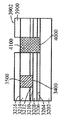
[0011]도 9 내지 도 15는 제 2 실시예에 따른 프로세싱 스테이지들 동안의 웨이퍼를 개략적으로 도시하는 입면도이다.
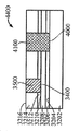
[0012]도 16 내지 도 23은 제 3 실시예에 따른 프로세싱 스테이지들 동안의 웨이퍼를 개략적으로 도시하는 입면도이다.
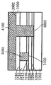
[0013]도 24 내지 도 31은 제 4 실시예에 따른 프로세싱 스테이지들 동안의 웨이퍼를 개략적으로 도시하는 입면도이다.
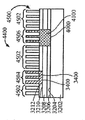
[0014]도 32 내지 도 45는 제 5 실시예에 따른 프로세싱 스테이지들 동안의 웨이퍼를 개략적으로 도시하는 입면도이다.
[0045]도 46 내지 도 52는 제 6 실시예에 따른 프로세싱 스테이지들 동안의 웨이퍼를 개략적으로 도시하는 입면도이다.
[0016]도 53은 일 실시예에 따른 방법을 도시하는 흐름도이다.
[0017]도 54는 다른 실시예에 따른 방법을 도시하는 흐름도이다.
[0018]도 55는 본 개시물의 실시예들이 사용될 수 있는 예시적인 무선 통신 시스템의 개략도이다.[0010] Figures 1-8 are elevational views schematically illustrating a wafer during different processing stages according to the first embodiment.
[0011] Figures 9-15 are elevational views schematically illustrating a wafer during processing stages according to a second embodiment.
[0012] Figures 16 through 23 are elevational views schematically illustrating a wafer during processing stages according to a third embodiment.
[0013] Figures 24-31 are elevational views schematically illustrating a wafer during processing stages according to a fourth embodiment.
[0014] Figures 32 through 45 are elevational views schematically illustrating a wafer during processing stages according to a fifth embodiment.
[0045] Figures 46-52 are elevational views schematically illustrating a wafer during processing stages according to a sixth embodiment.
[0016] Figure 53 is a flow chart illustrating a method in accordance with one embodiment.
[0017] FIG. 54 is a flowchart illustrating a method according to another embodiment.
[0018] Figure 55 is a schematic diagram of an exemplary wireless communication system in which embodiments of the present disclosure may be used.
[0019]본 발명의 양상들은 본 발명의 특정 실시예들과 관련된 다음 설명과 관련 도면들에 개시된다. 대안적인 실시예들은 본 발명의 범위로부터 벗어나지 않고 고안될 수 있다. 추가로, 본 발명의 잘 알려진 엘리먼트들은, 본 발명의 관련 상세들을 모호하게 하지 않도록 상세하게 설명되지 않거나 또는 생략될 것이다.[0019] Aspects of the present invention are set forth in the following description and the associated drawings that are related to specific embodiments of the invention. Alternate embodiments may be devised without departing from the scope of the present invention. In addition, well-known elements of the present invention will not be described in detail or will be omitted so as not to obscure the relevant details of the present invention.
[0020]단어 "예시적인"은 "예, 예시, 또는 예증으로서 기능하는"을 의미하도록 본원에 이용된다. "예시적인"으로서 본원에 설명된 어떠한 구현도 반드시 다른 실시예들에 비해 선호되거나 또는 유리한 것으로서 해석되지 않는다. 유사하게, 용어 "본 발명의 실시예들"은, 본 발명의 모든 실시예들이 논의된 특징, 이점, 또는 동작 모드를 포함하는 것을 요구하지 않는다.[0020] The word "exemplary" is used herein to mean "serving as an example, instance, or illustration." Any embodiment described herein as "exemplary " is not necessarily to be construed as preferred or advantageous over other embodiments. Similarly, the term "embodiments of the present invention" does not require that all embodiments of the present invention include the discussed features, advantages, or modes of operation.
[0021]본원에 사용된 용어는 특정 실시예들만을 설명하기 위한 것이고 본 발명의 실시예들을 제한하려는 것이 아니다. 본원에 사용된 바와 같이, 단수 표현들은, 문맥이 명시적으로 다르게 나타내지 않는다면 복수 형태들도 마찬가지로 포함하도록 의도된다. 용어들 "구비한다", "구비하는", "포함한다" 및/또는 "포함하는"은, 본원에서 사용될 경우, 언급된 특징들, 정수들, 단계들, 동작들, 엘리먼트들, 및/또는 컴포넌트들의 존재를 지정하지만, 하나 이상의 다른 특징들, 정수들, 단계들, 동작들, 엘리먼트들, 컴포넌트들 및/또는 이들의 그룹들의 존재 또는 추가를 배제하지 않는다는 것을 추가로 이해할 것이다.[0021] The terminology used herein is for the purpose of describing particular embodiments only and is not intended to limit the embodiments of the invention. As used herein, the singular forms are intended to include the plural forms as well, unless the context clearly indicates otherwise. The terms " comprising, "" comprising," " including, "and / or" comprising ", when used herein, include the referenced features, integers, But does not preclude the presence or addition of one or more other features, integers, steps, operations, elements, components, and / or groups thereof.
[0022]추가로, 많은 실시예들이, 예를 들어, 컴퓨팅 디바이스의 엘리먼트들에 의해 수행될 동작들의 시퀀스들에 관하여 설명되었다. 본원에 설명된 다양한 동작들은, 특정 회로들(예를 들어, ASIC(application specific integrated circuit)들)에 의해, 하나 이상의 프로세서들에 의해 실행되는 프로그램 명령들에 의해, 또는 이 둘의 결합에 의해 수행될 수 있다는 것을 인식할 것이다. 추가적으로, 본원에 설명된 동작들의 이러한 시퀀스는, 실행 시 연관된 프로세서로 하여금 본원에 설명된 기능을 수행하게 하는 컴퓨터 명령들의 대응하는 세트를 내부에 저장하고 있는 임의의 형태의 컴퓨터 판독가능 저장 매체 내에서 전적으로 구현되는 것으로 간주될 수 있다. 이와 같이, 본 발명의 다양한 양상들이 다수의 상이한 형태들로 구현될 수 있고, 이들 모두는 청구된 주제물의 범위 내에 있는 것으로 여겨진다. 이외에도, 본원에 설명된 실시예들 각각에 대해서, 임의의 이러한 실시예들의 대응하는 형태는, 예를 들어, 설명된 동작을 수행"하도록 구성된 로직"으로서 본원에서 설명될 수 있다.[0022] Additionally, many embodiments have been described with respect to sequences of operations to be performed, for example, by elements of a computing device. The various operations described herein may be performed by specific circuits (e.g., application specific integrated circuits (ASICs)), by program instructions executed by one or more processors, or by a combination of the two As shown in FIG. Additionally, this sequence of operations described herein may be implemented in any form of computer readable storage medium having stored thereon a corresponding set of computer instructions for causing the associated processor to perform the functions described herein It can be considered to be fully implemented. As such, various aspects of the present invention may be embodied in many different forms, all of which are considered to be within the scope of the claimed subject matter. In addition, for each of the embodiments described herein, the corresponding form of any of these embodiments may be described herein as, for example, "logic configured to perform the described operation ".
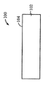
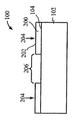
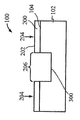
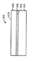
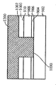
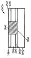
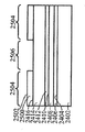
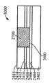
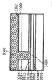
[0023]도 1은 상부 표면(104)을 구비한 실리콘 층(102)을 포함하는 기판(100)이다. 도 2에서, 상부 표면(202)을 갖는 질화물 하드 마스크(200)가, 기판(100)의 제 2 부분(206)은 마스킹하지 않은 상태로 기판(100)의 제 1 부분(204)에 제공되었다. 도 3에서, 에칭 프로세스는 기판의 마스킹되지 않은 제 2 부분(206)에서 기판(100)의 개구(300)를 형성했다. 도 4는, 질화물 하드마스크(200)의 상부 표면(202) 위에 그리고 개구(300) 내에 기판(100) 상에서 성장되거나 그렇지 않으면 형성되는 실리콘-게르마늄("SiGe") 층(400)을 도시한다. 유리하게, SiGe는 별개의 버퍼 층을 형성하지 않고 실리콘 상에 바로 성장될 수 있다. 도 5에서, SiGe층(400)이 질화물 하드마스크(200)의 상부 표면(202)의 레벨에 이르게 화학적으로 그리고/또는 기계적으로 제거되었다. SiGe를 산화시키는 것은 이것을 응축시키고, 다수의 산화물 프로세스들은 SiGe 층(400)의 높이를, SiGe 층(400)의 상부 표면(402)이 도 6에 도시된 바와 같이 실리콘 층(102)의 상부 표면(104)과 같은 평면이 될 때까지 감소시키고, 질화물 하드마스크(200)는 도 7에 도시된 바와 같이 제거된다. 이 결과는, 내부에 SiGe의 바디(400)가 포함되는 실리콘 층(102)을 포함하는 구조(700)이다. 복수의 핀들(800)이 도 8에 도시된 바와 같은 종래의 방식으로 구조(700)에 형성된다. 핀들의 제 1 서브셋(802)이 실리콘 층(102)으로 형성되고, 핀들의 제 2 서브셋(804)이 SiGe의 바디(400)로부터 형성된다. finFET 디바이스(미도시)가, 예를 들어, finFET 디바이스가 실리콘으로 형성된 일부 핀들과 게르마늄으로 형성된 다른 핀들을 구비하게 될 도 8의 디바이스로부터의 반도체 다이 상에 형성될 수 있다.[0023] FIG. 1 is a
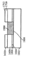
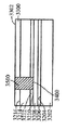
[0024]제 2 실시예에 따른 프로세스가 도 9 내지 도 15에 도시된다. 도 9는, 상부 표면(904)을 갖는 실리콘 층(902), 실리콘 층(902)의 상부 표면(904) 상의 하부 산화물층(906) 및 Ⅲ-Ⅴ족 재료, 이를 테면, 기판(900)이 통상적으로 "절연체 상의 Ⅲ-Ⅴ족"으로 지칭될 수 있는 인듐 비소화물 또는 인듐 갈륨 비소화물로 형성된 상부 층(908)을 포함하는 기판(900)을 도시한다. 상부 층(908)은 상부 표면(910)을 갖는다. 도 10에서, 상부 표면(1002)을 갖는 질화물 하드마스크(1000)가, 상부 층(908)의 제 2 부분(1006)은 노출된 상태로, 상부 층(908)의 상부 표면(910)의 제 1 부분(1004)에 제공된다. 도 11에 도시된 바와 같이, 상부 층(908)과 하부 산화물 층(906)이 에칭되어 실리콘 층(902)의 상부 표면(904)의 레벨에 이르게 개구(1100)를 형성한다. 도 12에서, SiGe 층(1200)이, 질화물 하드마스크(1000)의 개구(1100)에 그리고 상부 표면(1002) 상에 성장되거나 그렇지 않으면 형성된다. 제 1 실시예에서와 같이, SiGe 층(1200)이 버퍼 층을 사용하지 않고 실리콘 층(902) 상에 직접 성장될 수 있다. SiGe 층(1200)은 개구(1100) 안에 또는 개구(1100) 위에 있지 않은 그 부분들을 제거하기 위해 기계적으로 그리고/또는 화학적으로 개질되고, SiGe 층(1200)이 이후 산화되어 그의 두께를, 도 13에 도시된 바와 같이 상부 층(908)의 상부 표면(910)의 레벨까지 감소시킨다. 기판(1400)이 상부 층(908)에 SiGe의 바디(1200)를 갖는 Ⅲ-Ⅴ족 재료의 상부 층(908)을 포함한 상태로 도 14에 도시된 바와 같이 질화물 하드마스크(1000)가 제거된다. 도 15에서, 핀들(1500)은, Ⅲ-Ⅴ족 재료로부터 형성된 핀들(1502)의 제 1 서브셋과 SiGe로부터 형성된 핀들(1504)의 제 2 서브셋을 포함하는 기판(1400)으로부터 형성된다. finFET 디바이스(미도시)가 도 15의 디바이스로부터 형성될 수 있으며, finFET 디바이스는 Ⅲ-Ⅴ족 재료로 형성된 일부 핀들과 SiGe로 형성된 다른 핀들을 가질 것이다.[0024] The process according to the second embodiment is shown in FIGS. 9 shows a
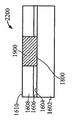
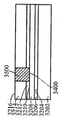
[0025]제 3 실시예에 따른 프로세스가 도 16 내지 도 23에 도시된다. 도 16에서, 상부 표면(1604)을 갖는 게르마늄 하부 층(1602)과 하부 층(1602)의 상부 표면(1604) 상의 산화물 층(1606)을 포함하는 기판(1600)이 제공된다. Ⅲ-Ⅴ족 상부 층(1608)은 산화물 층(1606) 상에 형성되며 상부 표면(1610)을 갖는다. 도 17에서, 제 2 부분(1706)은 노출된 상태로 상부 표면(1702)을 갖는 질화물 하드마스크(1700)가 상부 층(1608)의 제 1 부분(1704)에 제공된다. 도 18에서, 상부 층(1608)과 산화물 층(1606)이 게르마늄 하부 층(1602)의 상부 표면(1604)에 이르게 에칭되어 개구(1800)를 형성한다. 도 19는, 게르마늄의 바디(1900)가 질화물 하드마스크(1700)의 상부 표면(1702) 상에 그리고 개구(1800)에 비선택적으로 에피택셜 방식으로 증착되는 것을 도시한다. 하부 층(1602)과 바디(1900)가 둘 모두 게르마늄이기 때문에, SiGe를 사용할 필요가 없고, 대신에 바디(1900)의 게르마늄이 하부 층(1602)의 상부 표면(1604) 상에 직접 성장될 수 있다. 도 20은, 화학 기계적 연마 프로세스가 개구(1800) 외부에 있었던 게르마늄의 바디(1900)의 부분을 제거한 후의 기판(2000)을 도시하고, 도 21에서, 개구(1800)의 게르마늄의 바디(1900)가 산화되고 에칭되어 그 두께가 상부 층(1608)의 상부 표면(1610)의 레벨까지 감소한다. 질화물 하드마스크(1700)가 도 22에서 제거되어, 상부 층(1608)의 Ⅲ-Ⅴ족 재료로 둘러싸인 게르마늄의 바디(1900)를 갖는 기판(2200)이 생성된다. 이 기판(2200)이 프로세싱되어 도 23에서 핀들(2300)을 형성하고, 핀들 중 제 1 서브셋(2302)은 Ⅲ-Ⅴ족 재료로 형성되고 핀들 중 제 2 서브셋(2304)은 바디(1900)로부터의 게르마늄으로 형성된다. finFET 디바이스(미도시)는 도 23의 디바이스로부터 형성될 수 있고, finFET 디바이스는 Ⅲ-Ⅴ족 재료로 형성된 일부 핀들과 게르마늄으로 형성된 다른 핀들을 가질 것이다.[0025] The process according to the third embodiment is shown in FIGS. 16, a
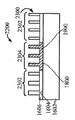
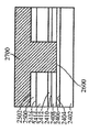
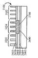
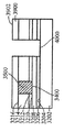
[0026]제 4 실시예에 따른 프로세스가 도 24 내지 도 31에 도시된다. 도 24는, 상부 표면(2404)을 갖는 실리콘 층(2402), 제 1 산화물 층(2406), 제 1 산화물 층(2406) 상의 상부 표면(2410)을 갖는 게르마늄 층(2408), 상부 표면(2410) 상의 제 2 산화물 층(2412), 및 상부 표면(2416)을 갖는 Ⅲ-Ⅴ족 상부 계층(2414)을 갖는 기판(2400)을 도시한다. 도 25에서, 상부 층(2414)의 제 2 부분(2506)을 노출된 상태로 상부 표면(2502)을 갖는 질화물 하드마스크(2500)가 상부 층(2414)의 제 1 부분(2504)에 제공된다. 도 26에서, 상부 층(2414) 및 제 2 산화물 층(2412)이 제 2 부분(2506)에서 게르마늄 층(2408)의 상부 표면(2410)에 이르게 에칭되어 개구(2600)를 형성한다. 도 27에 도시된 바와 같이, 게르마늄의 바디(2700)가 개구(2600) 밖으로 그리고 질화물 하드마스크(2500)의 상부 표면(2502) 상으로 확장되도록 개구(2600)에서 성장된다. 게르마늄의 바디(2700)가 게르마늄 층(2408) 상에서 성장되기 때문에, 별개의 버퍼 층이 요구되지 않는다. 이후, 도 28에 도시된 바와 같이, 질화물 하드마스크(2500)의 상부 표면(2502) 상의 바디(2700)의 부분이 화학적으로 그리고/또는 기계적으로 제거되고, 도 29에서, 게르마늄의 바디(2700)가 산화되고 에칭되어 그의 두께가 상부 층(2414)의 상부 표면(2416)의 레벨까지 감소한다. 도 30에서, 질화물 하드마스크(2500)가 제거되고 기판(3000)은 내부에 게르마늄 바디(2700)를 갖는 Ⅲ-Ⅴ족 재료의 상부 층(2414)을 포함한다. 기판(3000)은 도 31에 도시된 핀들(3100)을 형성하는 종래의 방식으로 프로세싱되며, 핀들 중 제 1 서브셋(3102)은 Ⅲ-Ⅴ족 재료로 형성되고 핀들 중 제 2 서브셋(3104)은 게르마늄의 바디(2700)로부터 게르마늄으로 형성된다. finFET 디바이스(미도시)는 도 31의 디바이스로부터 형성될 수 있고, finFET 디바이스는 Ⅲ-Ⅴ족 재료로 형성된 일부 핀들과 게르마늄으로 형성된 다른 핀들을 가질 것이다.[0026] The process according to the fourth embodiment is shown in FIGS. 24 shows a
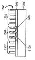
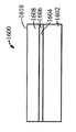
[0027]앞의 설명으로부터, 도 24 내지 도 31의 실시예는 도 16 내지 도 23의 실시예와 다소 유사하다는 것을 인식할 것이다. 그러나, 게르마늄 층(2408)을 실리콘 기판(2400)에 제공하는 것은, 기판으로 하여금, 상부에 게르마늄 바디(2700)를 성장시키는 게르마늄 층(2408)을 여전히 제공하면서 실리콘을 프로세싱하기 위한 종래의 장비로 다루어질 수 있게 한다. 도 16 내지 도 23의 기판(1600)은 도 24 내지 도 31의 방법과 유사한 방식으로 핀들을 형성하기 위해 사용될 수 있지만, 이것이 게르마늄 하부 층(1602)을 포함하기 때문에, 기판(1600)은, 재료가 통상적으로 실리콘보다 더 손상되기 쉽고 취급하기 더 곤란한 게르마늄을 취급하도록 특별히 구성된 장비에 의해 프로세싱되어야 한다.[0027] From the foregoing description, it will be appreciated that the embodiment of Figures 24-31 is somewhat similar to the embodiment of Figures 16-23. Providing the
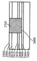
[0028]도 32 내지 도 45는 제 5 실시예에 따른 프로세스를 도시하며, 여기서 3개의 상이한 재료들의 핀들이 기판 상에 형성된다. 도 32는 상부 표면(3204)을 갖는 실리콘 층(3202), 제 1 산화물 층(3206), 제 1 산화물 층(3206) 상의 상부 표면(3210)을 갖는 게르마늄 층(3208), 상부 표면(3210) 상의 제 2 산화물 층(3212), 및 상부 표면(3216)을 갖는 Ⅲ-Ⅴ족 상부 층(3214)을 갖는 기판(3200)을 도시한다. 도 33에서, 상부 층(3214)의 제 2 부분(3306)을 노출된 상태로 상부 표면(3302)을 갖는 질화물 하드마스크(3300)가 상부 층(3214)의 제 1 부분(3304)에 제공된다. 도 34에서, 상부 층(3214) 및 제 2 산화물 층(3212)이 제 2 부분(3306)에서 게르마늄 층(3208)의 상부 표면(3210)에 이르게 에칭되어 개구(3400)를 형성한다. 도 35는, 게르마늄의 바디(3500)가 개구(3400) 밖으로 그리고 질화물 하드마스크(3300)의 상부 표면(3302) 상으로 확장되도록 개구(3400)에서 성장되는 것을 도시한다. 게르마늄의 바디(3500)가 게르마늄 층(3208) 상에서 성장되기 때문에, 별개의 버퍼 층이 요구되지 않는다. 이후, 도 36에 도시된 바와 같이, 질화물 하드마스크(3300)의 상부 표면(3302) 상의 바디(3500)의 부분이 화학적으로 그리고/또는 기계적으로 제거되고, 도 37에서, 게르마늄의 바디(3500)가 산화되고 에칭되어 그의 두께가 상부 층(3214)의 상부 표면(3216)의 레벨까지 감소한다. 도 38에서, 질화물 하드마스크(3300)가 제거되고 기판은 내부에 게르마늄 바디(3500)를 갖는 Ⅲ-Ⅴ족 재료의 상부 층(3214)을 포함하며, 기판은 Ⅲ-Ⅴ족 재료의 상부 층(3214)의 상부를 포함하는 상부 표면을 구비한다.[0028] Figures 32-45 illustrate a process according to the fifth embodiment, wherein pins of three different materials are formed on a substrate. 32 shows a
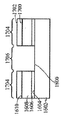
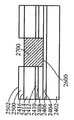
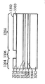
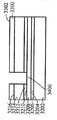
[0029]이 점에서,제 5 실시예의 프로세스가 제 4 실시예의 프로세스와 유사하다. 그러나, 내부에 게르마늄 바디(3500)를 갖는 기판이 형성된 후, 본 실시예에서, 도 39에 도시된 바와 같이, 상부 표면(3902)을 갖는 제 2 질화물 하드 마스크(3900)가 기판의 상부 표면(3802) 상에 형성되며, 제 2 부분(3306)로부터 이격되는 위치에 제 3 부분(3904)이 노출된 상태로 있다. 도 40에 도시된 바와 같이, 상부 층(3214), 제 2 산화물 층(3212), 게르마늄 층(3208) 및 제 1 산화물 층(3206)이 에칭되어, 실리콘 층(3202)의 상부 표면(3204)으로 확장되는 개구(4000)를 형성하고, 도 41에서, 실리콘의 바디(4100)가 실리콘 층(3202)의 상부 표면(3204) 상에 형성되어, 실리콘의 바디는 개구(4000)를 충진하고 질화물 하드마스크(3900)의 상부 표면(3902)을 커버한다. 실리콘의 바디(4100)는, 이것이 상부 층(3214)의 상부 표면(3216)의 레벨이 될 때까지, 도 43에 도시된 바와 같이, 질화물 하드마스크의 상부 표면(3902)로부터 화학적으로 그리고/또는 기계적으로 제거되고 산화된다. 도 44에 도시된 바와 같이, 기판(4400)이 Ⅲ-Ⅴ족 재료의 상부 층(3214)에 게르마늄의 제 1 지역(3500)과 실리콘의 제 2 지역(4100)을 갖는 상태로, 제 2 질화물 하드마스크(3900)가 제거된다. 이 기판(4400)이 도 45에 도시된 바와 같이 복수의 핀들(4500)을 형성하기 위해 종래의 방식으로 프로세싱된다. 핀들(4500)의 제 1 서브셋(4502)이 Ⅲ-Ⅴ족 재료를 포함하고, 핀들(4500)의 제 2 서브셋(4504)이 게르마늄 바디(3500)로부터의 게르마늄을 포함하고, 핀들(4500)의 제 3 서브셋(4506)이 실리콘의 제 2 지역(4100)으로부터의 실리콘을 포함한다. 기존의 게르마늄 층(3208) 상에서 게르마늄을 성장시키는 것과 실리콘 층(3202) 상에서 실리콘을 성장시키는 것은, 상이한 재료들 각각을 위한 버퍼 층을 형성할 필요 없이 finFET(미도시)에 사용하기 위한 3가지 상이한 타입의 핀들의 형성을 가능하게 한다.In this respect, the process of the fifth embodiment is similar to the process of the fourth embodiment. 39, a second nitride
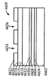
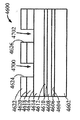
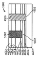
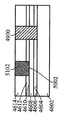
[0030]도 46 내지 도 51은 제 6 실시예에 따른 방법을 도시한다. 이 실시예에서, 도 46을 참고하면, 실리콘 기판(4600)은, 상부 표면(4604)을 갖는 실리콘 층(4602), 상부 표면(4604) 상의 제 1 산화물 층(4606), 제 1 산화물 층(4606) 상에 있고 상부 표면(4610)을 갖는 게르마늄 층(4608), 게르마늄 층(4608)의 상부 표면(4610) 상의 제 2 산화물 층(4612)을 갖는다. Ⅲ-Ⅴ족 재료를 포함하고 상부 표면(4616)을 갖는 상부 층(4614)이 제 2 산화물 층(4612) 상에 형성된다. 상부 표면(4620)을 갖는 질화물 하드마스크(4618)가 상부 층(4614)의 상부 표면(4616) 상에 형성된다. 이 구조는 도 33의 구조와 전반적으로 유사하다. 그러나, 이전 실시예에서, 실리콘의 핀들을 형성하기 위한 위치가 게르마늄의 핀들을 형성하기 위한 위치와 무관하게 결정되었다. 본 실시예는, 핀들의 이러한 2개의 세트들의 상대적인 위치들의 보다 정확한 제어를 가능하게 한다. 이를 위해, 상부 마스크 층(4622)이 질화물 하드마스크(4618)의 상부 표면(4620)에 제공되는데, 게르마늄 핀들을 형성하기 위한 위치에 제 1 개구(4624)가 있고 실리콘 핀들을 형성하기 위한 위치에 제 2 개구(4626)가 있으며, 도 47에서 도시된 바와 같이, 제 1 개구(4700)가 제 1 개구(4624)에서 질화물 하드마스크(4618)에 에칭되고 제 2 개구(4702)가 제 2 개구(4626)에서 질화물 하드마스크(4618)에 에칭된다. 도 48에서, 제 1 개구가 재료(4800)의 쉴드 바디, BARC(bottom anti-reflective material), 또는 예를 들어, 스핀 코팅 이후 리소그래픽 및 현상(development) 프로세스에 의해 형성될 수 있는 막을 포함하는 포토레지스터 또는 유기 탄소로 충진된다. 대안으로, 재료(4800)의 바디는 탄소-도핑 SiOx를 포함할 수 있고 PECVD(plasma enhanced chemical vapor deposition) 프로세스에 의해 증착된 다음 리소그래픽 프로세스를 거친 후 에칭된다. 제 2 개구(4626)에서, 기판(4600)이 상부 층(4614), 제 2 산화물 층(4612), 게르마늄 층(4608) 및 제 1 산화물 층(4606)을 통과하여 실리콘 층(4602)까지 에칭되어 개구(4802)를 형성한다. 도 49에서, 실리콘의 바디(4900)가 상부 마스크 층(4622)까지 개구(4802)에서 성장된다. 후속하여, 도 50에 도시된 바와 같이, 재료(4800)의 쉴드 바디가 제거되고, 개구(5002)가 상부 마스크 층(4622)의 제 1 개구(4624)에 형성된다. 이러한 추가 개구(5002)에서, 상부 층(4614)과 제 2 산화물 층(4612)이 게르마늄 층(4608)의 레벨까지 에칭되고, 도 51에 도시된 바와 같이, 게르마늄의 바디(5102)가 상부 마스크 층(4622)까지 개구(5002)에서 성장된다. 상부 마스크 층(4622) 및 질화물 하드마스크(4618)는 이후에, 기판(5200)이 Ⅲ-Ⅴ족 재료로 형성된 상부 계층(4614)에 의해 각각 둘러싸인 게르마늄 바디(5102)와 실리콘 바디(4900)를 갖는 상태가 되도록 제거되며, 여기서 기판은 도 45에 도시된 바와 같이 실질적으로 3개의 상이한 타입들의 핀들을 갖는 기판으로 형성될 수 있다.[0030] Figures 46 to 51 illustrate a method according to a sixth embodiment. 46, a
[0031]일 실시예에 따른 방법이 도 53에 도시되며 상부 표면을 갖는 제 1 재료의 층을 포함하는 기판을 제공하는 블록(5300), 기판의 제 2 부분을 노출된 상태로 두고 기판의 제 1 부분을 마스킹하는 블록(5302), 제 2 부분에 제 1 개구를 에칭하는 블록(5304), 개구 내의 제 2 재료의 바디를 제 1 재료의 층의 상부 표면의 레벨까지 형성하는 블록(5306), 마스크를 제거하는 블록(5308) 및 제 1 부분에 제 1 재료의 핀들을 형성하고 제 2 부분에 제 2 재료의 핀들을 형성하는 블록(5310)을 포함한다.[0031] A method according to one embodiment is shown in Figure 53, comprising a
일 실시예에 따른 다른 방법이 도 54에 도시되며, 제 1 재료의 층, 제 1 재료의 층 상의 제 1 산화물 층, 제 1 산화물 층 상의 제 2 재료의 층, 제 2 재료의 층 상의 제 2 산화물 층 및 제 2 산화물 층 상의 제 3 재료의 층을 포함하는 기판을 제공하는 블록(5400)을 포함하고, 제 3 재료의 층은 기판의 상부 표면을 형성하는 상부 표면을 갖는다. 방법은 또한, 제 3 재료의 층을 통과하고 제 2 산화물 층을 통과하여 제 2 재료의 층까지 기판 상의 제 1 위치에서 제 1 개구를 에칭하는 블록(5402), 기판의 상부 표면의 레벨까지 제 1 개구에 제 2 재료의 바디를 형성하는 블록(5404), 제 3 재료의 층, 제 2 산화물 층, 제 2 재료의 층 및 제 1 산화물 층을 통과하여 제 1 재료의 층까지 기판 상의 제 2 위치에서 제 2 개구를 에칭하는 블록(5406), 기판의 상부 표면의 레벨까지 제 2 개구에 제 1 재료의 바디를 형성하는 블록(5408) 및 제 1 위치에 제 2 재료를 포함하는 제 1 핀들을 형성하고, 제 2 위치에 제 1 재료를 포함하는 제 2 핀들을 형성하고 제 3 위치에 제 3 재료를 포함하는 제 3 핀들을 형성하는 블록(5410)을 포함한다.Another method according to one embodiment is shown in Figure 54, wherein a layer of a first material, a layer of a first material on a layer of a first material, a layer of a second material on a layer of a first material, A layer of a third material on the oxide layer and a layer of a third material on the second oxide layer, the layer of third material having a top surface forming the top surface of the substrate. The method also includes a
[0032]도 55는, 본 개시물의 하나 이상의 실시예들이 유리하게 채용될 수 있는 예시적인 무선 통신 시스템(5500)을 도시한다. 예시를 위해서, 도 55는 3개의 원격 유닛들(5520, 5530, 및 5550) 및 2개의 기지국들(5540)을 도시한다. 종래의 무선 통신 시스템들은 더 많은 원격 유닛들과 기지국들을 가질 수 있다는 것을 인식할 것이다. 원격 유닛들(5520, 5530 및 5550)은, 본 개시물의 실시예들 중에서 아래에 추가로 설명된 바와 같은 (본원에 개시된 바와 같은 상이한 재료들의 핀들을 갖는 finFET를 포함한) 다른 반도체 디바이스들(5525, 5535 및 5555) 또는 집적 회로를 포함한다. 도 55는 기지국들(5540)으로부터 원격 유닛들(5520, 5530 및 5550)으로의 순방향 링크 신호들(5580)과 원격 유닛들(5520, 5530 및 5550)로부터 기지국들(5540)로의 역방향 링크 신호들(5590)을 도시한다.[0032] FIG. 55 illustrates an exemplary
[0033]도 55에서, 원격 유닛(5520)은 모바일 전화기로 도시되고, 원격 유닛(5530)은 휴대용 컴퓨터로 도시되고, 원격 유닛(5550)은 무선 로컬 루프 시스템의 고정 위치 원격 유닛으로 도시된다. 예를 들어, 원격 유닛들은 모바일 전화, 휴대용 PCS(personal communication system) 유닛, 휴대용 데이터 유닛 이를 테면 PDA(personal data or digital assistant), 내비게이션 디바이스(이를 테면, 헨 인에이블드 디바이스들), 셋톱 박스, 뮤직 플레이어, 비디오 플레이어, 엔터테인먼트 유닛, 고정 위치 데이터 유닛 이를 테면 검침 장비, 또는 데이터 또는 컴퓨터 명령들, 또는 이들의 임의의 조합을 저장하거나 또는 리트리빙하는 임의의 다른 디바이스 중 어느 하나 또는 조합일 수 있다. 도 55가 본 개시물의 교시들에 따른 원격 유닛들을 도시하지만, 본 개시물은 이러한 예시적인 도시된 유닛들로 제한되지 않는다. 본 개시물의 실시예들은, 테스트 및 특징부여(characterization)를 위한 온-칩 회로소자 및 메모리를 포함하는 능동 집적 회로를 구비한 임의의 디바이스에서 적절하게 채용될 수 있다.In FIG. 55, the
[0034]당업자들은, 본원에 개시된 실시예들과 관련하여 설명된 다양한 예시적인 로직 블록들, 모듈들, 회로들, 및 알고리즘 단계들이 전자 하드웨어, 컴퓨터 소프트웨어, 또는 이 둘의 결합들로서 구현될 수도 있음을 추가적으로 인식할 것이다. 하드웨어와 소프트웨어의 이러한 상호교환가능성을 명확히 예시하기 위해, 다양한 예시적인 컴포넌트들, 블록들, 모듈들, 회로들, 및 단계들은 그들의 기능성의 관점들에서 일반적으로 상술되었다. 그러한 기능이 하드웨어로 구현되는지 또는 소프트웨어/펌웨어로 구현되는지 여부는 특정 애플리케이션, 및 전체 시스템에 부과된 설계 제약들에 의존한다. 당업자들은 설명된 기능을 각각의 특정 애플리케이션에 대해 다양한 방식들로 구현할 수도 있지만, 그러한 구현 결정들이 본 발명의 범위를 벗어나게 하는 것으로서 해석되지는 않아야 한다.[0034] Those skilled in the art will appreciate that the various illustrative logical blocks, modules, circuits, and algorithm steps described in connection with the embodiments disclosed herein may be implemented as electronic hardware, computer software, or combinations of both . ≪ / RTI > To clearly illustrate this interchangeability of hardware and software, various illustrative components, blocks, modules, circuits, and steps have been described above generally in terms of their functionality. Whether such functionality is implemented in hardware or software / firmware depends upon the particular application and design constraints imposed on the overall system. Skilled artisans may implement the described functionality in varying ways for each particular application, but such implementation decisions should not be interpreted as causing a departure from the scope of the present invention.
[0035]본원에 개시된 실시예들과 관련하여 설명된 방법, 시퀀스들 및/또는 알고리즘들은 직접 하드웨어로, 프로세서에 의해 실행되는 소프트웨어 모듈로, 또는 이 둘의 결합으로 구현될 수도 있다. 소프트웨어/펌웨어 모듈은 RAM 메모리, 플래시 메모리, ROM 메모리, EPROM 메모리, EEPROM 메모리, 레지스터들, 하드디스크, 착탈형 디스크, CD-ROM, 또는 당업계에 알려진 임의의 다른 형태의 저장 매체에 상주할 수도 있다. 예시적인 저장 매체는, 프로세서가 저장 매체로부터 정보를 판독하고, 저장 매체에 정보를 기입할 수 있도록 프로세서에 커플링된다. 대안적으로, 저장 매체는 프로세서에 통합될 수도 있다.[0035] The methods, sequences and / or algorithms described in connection with the embodiments disclosed herein may be embodied directly in hardware, in a software module executed by a processor, or in a combination of the two. The software / firmware module may reside in RAM memory, flash memory, ROM memory, EPROM memory, EEPROM memory, registers, a hard disk, a removable disk, a CD-ROM, or any other form of storage medium known in the art . An exemplary storage medium is coupled to the processor such that the processor can read information from, and write information to, the storage medium. Alternatively, the storage medium may be integral to the processor.
[0036]그에 따라, 본 발명의 실시예는 상이한 재료들로 이루어진 핀들을 갖는 기판을 형성하기 위한 방법을 구현하는 컴퓨터 판독가능 매체를 포함할 수 있다. 그에 따라, 본 발명은 예시된 실시예들로 제한되지 않으며 본원에 설명된 기능을 수행하기 위한 임의의 수단이 본 발명의 실시예들에 포함된다.Accordingly, embodiments of the present invention may include a computer readable medium embodying a method for forming a substrate having pins of different materials. Accordingly, the present invention is not limited to the illustrated embodiments, and any means for performing the functions described herein are included in embodiments of the present invention.
[0037]앞의 개시물은 본 발명의 예시적인 실시예들을 나타내지만, 다양한 변경들 및 수정들이 첨부된 청구범위에 의해 정의된 바와 같이 본 발명의 범위로부터 벗어나지 않고 본원에서 이루어질 수 있다는 것을 주목해야 한다. 본원에 설명된 본 발명의 실시예들에 따른 방법 청구항들의 기능들, 단계들 및/또는 동작들은 임의의 특정 순서로 수행될 필요가 없다. 또한, 본 발명의 엘리먼트들이 단수로 기술되거나 청구될 수 있지만, 단수로의 제한이 명시적으로 언급되지 않는다면 복수로 간주된다.[0037] It should be noted that while the foregoing disclosure illustrates exemplary embodiments of the invention, various changes and modifications may be made herein without departing from the scope of the invention as defined by the appended claims do. The functions, steps and / or operations of the method claims according to embodiments of the invention described herein need not be performed in any particular order. In addition, elements of the invention may be described or claimed in the singular, but are construed as plural unless limitation to the singular is explicitly stated.
Claims (27)
상부 표면을 갖는 제 1 재료의 층을 포함하는 기판을 제공하는 단계;
상기 기판의 제 2 부분을 노출시킨 상태로 마스크를 형성시키기 위해 상기 기판의 제 1 부분을 마스킹하는 단계;
상기 제 2 부분에 제 1 개구를 에칭하는 단계;
상기 제 1 재료의 층의 상기 상부 표면의 레벨까지 상기 제 1 개구에 제 2 재료의 바디를 형성하는 단계;
상기 마스크를 제거하는 단계; 및
상기 제 1 부분에 상기 제 1 재료의 핀들을 형성하고 상기 제 2 부분에 상기 제 2 재료의 핀들을 형성하는 단계를 포함하는, 상이한 재료들의 핀들을 형성하는 방법.1. A method of forming pins made of different materials,
Providing a substrate comprising a layer of a first material having an upper surface;
Masking a first portion of the substrate to form a mask while exposing a second portion of the substrate;
Etching the first opening in the second portion;
Forming a body of a second material in the first opening to a level of the upper surface of the layer of first material;
Removing the mask; And
Forming fins of the first material in the first portion and forming fins of the second material in the second portion.
상기 제 1 재료는 실리콘인, 상이한 재료들의 핀들을 형성하는 방법.The method according to claim 1,
Wherein the first material is silicon.
상기 제 1 재료는 Ⅲ-Ⅴ족 재료인, 상이한 재료들의 핀들을 형성하는 방법.The method according to claim 1,
Wherein the first material is a Group III-V material.
상기 제 2 재료는 게르마늄인, 상이한 재료들의 핀들을 형성하는 방법.The method of claim 3,
Wherein the second material is germanium.
상기 제 2 재료는 실리콘 게르마늄인, 상이한 재료들의 핀들을 형성하는 방법.The method of claim 3,
Wherein the second material is silicon germanium.
상기 기판은 상기 제 2 재료의 층 및 상기 제 2 재료의 층 상의 제 1 산화물의 층을 포함하고, 상기 제 1 재료의 층은 상기 제 1 산화물의 층 상에 위치되고, 상기 제 2 부분에서 제 1 개구를 에칭하는 단계는 상기 제 1 재료의 층과 상기 제 1 산화물의 층을 통과하여 상기 제 2 재료의 층까지 제 1 개구를 에칭하는 단계를 포함하는, 상이한 재료들의 핀들을 형성하는 방법.The method of claim 3,
Wherein the substrate comprises a layer of the second material and a layer of a first oxide on the layer of the second material, the layer of the first material being located on the layer of the first oxide, Wherein etching the first opening comprises etching a first opening through a layer of the first material and a layer of the first oxide to a layer of the second material.
상기 기판은 제 3 재료의 층과 상기 제 3 재료의 층 상의 제 1 산화물의 층을 포함하고, 상기 제 1 재료의 층은 상기 제 1 산화물의 층 상에 위치되고, 상기 제 2 부분에서 제 1 개구를 에칭하는 단계는 상기 제 1 재료의 층과 상기 제 1 산화물의 층을 통과하여 상기 제 3 재료의 층까지 제 1 개구를 에칭하는 단계를 포함하는, 상이한 재료들의 핀들을 형성하는 방법.The method of claim 3,
Wherein the substrate comprises a layer of a third material and a layer of a first oxide on a layer of the third material, the layer of the first material being located on the layer of the first oxide, Wherein etching the opening comprises etching a first opening through the layer of first material and the layer of first oxide to a layer of the third material.
상기 제 3 재료는 실리콘이고 상기 제 2 재료는 실리콘-게르마늄인, 상이한 재료들의 핀들을 형성하는 방법.8. The method of claim 7,
Wherein the third material is silicon and the second material is silicon-germanium.
상기 기판은 제 3 재료의 층, 상기 제 3 재료의 층 상의 제 1 산화물 층, 상기 제 1 산화물 층 상의 제 2 재료의 층, 및 상기 제 2 재료의 층 상의 제 2 산화물 층을 포함하고, 상기 제 1 재료의 층은 상기 제 2 산화물 층 상에 위치되고, 상기 제 2 부분에서 제 1 개구를 에칭하는 단계는 상기 제 1 재료의 층과 상기 제 2 산화물 층을 통과하여 상기 제 2 재료의 층까지 제 1 개구를 에칭하는 단계를 포함하는, 상이한 재료들의 핀들을 형성하는 방법.The method according to claim 1,
Wherein the substrate comprises a layer of a third material, a first oxide layer on the layer of the third material, a layer of a second material on the first oxide layer, and a second oxide layer on the layer of the second material, Wherein a layer of a first material is located on the second oxide layer and etching of the first opening in the second portion comprises passing the layer of first material through the second oxide layer, And etching the first openings to form the first openings.
상기 기판의 제 3 부분에서 상기 제 1 재료의 층, 상기 제 2 산화물 층, 상기 제 2 재료의 층 및 상기 제 1 산화물 층을 통과하여 상기 제 3 재료의 층까지 제 2 개구를 에칭하는 단계 및 상기 제 1 재료의 층의 상기 상부 표면의 레벨까지 상기 제 2 개구에 상기 제 3 재료의 바디를 형성하는 단계 및 상기 제 3 재료의 핀들을 상기 제 3 부분에 형성하는 단계를 포함하는, 상이한 재료들의 핀들을 형성하는 방법.10. The method of claim 9,
Etching a second opening through the layer of the first material, the second oxide layer, the layer of the second material, and the first oxide layer to a layer of the third material in a third portion of the substrate; and Forming a body of said third material in said second opening to a level of said upper surface of said layer of said first material and forming pins of said third material in said third portion; / RTI >
상기 기판의 제 1 부분을 마스킹하는 단계는 상기 기판의 제 3 부분을 노출된 상태로 두는 단계를 포함하고, 그리고 상기 제 1 재료의 층, 상기 제 2 산화물 층, 상기 제 2 재료의 층 및 상기 제 1 산화물 층을 통과하여 상기 제 3 재료의 층까지 상기 기판의 상기 제 3 부분에서 제 2 개구를 에칭하는 단계 및 상기 제 1 재료의 층의 상기 상부 표면의 레벨까지 상기 제 2 개구에 상기 제 3 재료의 바디를 형성하는 단계 및 상기 제 3 부분에서 상기 제 3 재료의 핀들을 형성하는 단계를 포함하는, 상이한 재료들의 핀들을 형성하는 방법.10. The method of claim 9,
Wherein masking the first portion of the substrate comprises placing a third portion of the substrate in an exposed state and wherein the layer of the first material, the layer of the second oxide, the layer of the second material, Etching a second opening in the third portion of the substrate through a first oxide layer to a layer of the third material and etching the second opening to a level of the upper surface of the layer of first material, 3 material; and forming the fins of the third material in the third portion. ≪ Desc / Clms Page number 13 >
상부 표면을 갖는 제 1 층을 갖는 기판;
상기 제 1 층의 상부 표면 상의 제 1 산화물 층 ―상기 제 1 산화물 층은 상부 표면을 갖고, 상기 제 1 산화물 층은 상기 제 1 층의 제 1 부분을 커버하고 상기 제 1 층의 제 2 부분은 커버하지 않음―;
상기 제 1 층의 상기 제 2 부분에 있는 재료의 제 1 바디 ―상기 재료의 제 1 바디는 상기 제 1 산화물 층의 상기 상부 표면과 동일 평면에 있는 상부 표면을 가짐―;
상기 제 1 산화물 층 상의 제 1 재료로 형성된 핀들의 제 1 세트; 및
상기 재료의 제 1 바디 상에 제 2 재료로 형성된 핀들의 제 2 세트를 포함하는, 적어도 2개의 상이한 재료들로 형성된 핀들을 갖는 finFET 디바이스.A finFET device having pins formed of at least two different materials,
A substrate having a first layer having an upper surface;
A first oxide layer on the upper surface of the first layer, the first oxide layer having a top surface, the first oxide layer covering a first portion of the first layer and the second portion of the first layer Do not cover -;
A first body of material in the second portion of the first layer, the first body of material having an upper surface coplanar with the upper surface of the first oxide layer;
A first set of fins formed of a first material on the first oxide layer; And
And a second set of fins formed of a second material on a first body of the material.
상기 제 1 층은 상기 제 2 재료를 포함하는, 적어도 2개의 상이한 재료들로 형성된 핀들을 갖는 finFET 디바이스.13. The method of claim 12,
Wherein the first layer comprises the second material and the fins formed of at least two different materials.
상기 기판은 상기 제 1 재료 및 상기 제 2 재료와 상이한 제 3 재료를 포함하는, 적어도 2개의 상이한 재료들로 형성된 핀들을 갖는 finFET 디바이스.13. The method of claim 12,
Wherein the substrate comprises fins formed of at least two different materials, wherein the fins comprise a third material different from the first material and the second material.
상기 제 2 재료는 게르마늄을 포함하는, 적어도 2개의 상이한 재료들로 형성된 핀들을 갖는 finFET 디바이스.15. The method of claim 14,
Wherein the second material comprises germanium. ≪ RTI ID = 0.0 >< / RTI >
상기 기판은 상기 제 2 층과 상기 제 2 층 상의 제 2 산화물 층을 포함하고, 상기 제 1 층은 상기 제 2 산화물 층 상에 위치되고, 그리고 상기 제 2 층으로부터 상기 제 2 산화물 층, 상기 제 1 층 및 제 1 산화물 층을 통과하여 확장되는 재료의 제 2 바디― 상기 재료의 제 2 바디는 상기 제 1 산화물 층의 상기 상부 표면과 동일 평면에 있는 상부 표면을 갖고, 상기 재료의 제 2 바디와 상기 제 2 층은 제 3 재료로 형성됨―, 및 상기 재료의 제 2 바디 상에 상기 제 3 재료로 형성되는 핀들의 제 3 세트를 포함하는, 적어도 2개의 상이한 재료들로 형성된 핀들을 갖는 finFET 디바이스.15. The method of claim 14,
Wherein the substrate comprises a second oxide layer on the second layer and the second layer, the first layer is located on the second oxide layer, and the second oxide layer, the second oxide layer, A second body of material extending through the first layer and the first oxide layer, the second body of material having a top surface coplanar with the top surface of the first oxide layer, And a fin formed of at least two different materials, wherein the second layer is formed of a third material, and a third set of fins formed of the third material on a second body of the material. device.
상기 제 2 재료는 게르마늄을 포함하고 상기 제 3 재료는 실리콘을 포함하는, 적어도 2개의 상이한 재료들로 형성된 핀들을 갖는 finFET 디바이스.17. The method of claim 16,
Wherein the second material comprises germanium and the third material comprises silicon. ≪ RTI ID = 0.0 > 15. < / RTI >
적어도 하나의 반도체 다이에 통합되는, 적어도 2개의 상이한 재료들로 형성된 핀들을 갖는 finFET 디바이스.13. The method of claim 12,
A finFET device having fins formed of at least two different materials, integrated into at least one semiconductor die.
제 1 재료의 층, 상기 제 1 재료의 층 상의 제 1 산화물 층, 상기 제 1 산화물 층 상의 제 2 재료의 층, 상기 제 2 재료의 층 상의 제 2 산화물 층 및 상기 제 2 산화물 층 상의 제 3 재료의 층을 포함하는 기판을 제공하는 단계 ―상기 제 3 재료의 층은 상기 기판의 상부 표면을 형성하는 상부 표면을 가짐―;
상기 제 3 재료의 층을 통과하고 상기 제 2 산화물 층을 통과하여 상기 제 2 재료의 층까지 상기 기판 상의 제 1 위치에서 제 1 개구를 에칭하는 단계;
상기 기판의 상기 상부 표면의 레벨까지 상기 제 1 개구에 상기 제 2 재료의 바디를 형성하는 단계;
상기 제 3 재료의 층, 상기 제 2 산화물 층, 상기 제 2 재료의 층 및 상기 제 1 산화물 층을 통과하여 상기 제 1 재료의 층까지 상기 기판 상의 제 2 위치에서 제 2 개구를 에칭하는 단계;
상기 기판의 상기 상부 표면의 레벨까지 상기 제 2 개구에 상기 제 1 재료의 바디를 형성하는 단계; 및
상기 제 1 위치에서 상기 제 2 재료를 포함하는 제 1 핀들을 형성하고, 상기 제 2 위치에서 상기 제 1 재료를 포함하는 제 2 핀들을 형성하고, 그리고 제 3 위치에서 상기 제 3 재료를 포함하는 제 3 핀들을 형성하는 단계를 포함하는, 상이한 재료들로 이루어진 핀들을 형성하는 방법.1. A method of forming pins made of different materials,
A first oxide layer on the first material layer, a second oxide layer on the first material layer, a second oxide layer on the second material layer, and a third oxide layer on the second oxide layer, Providing a substrate comprising a layer of material, the layer of third material having an upper surface forming an upper surface of the substrate;
Etching the first opening through the layer of third material and through the second oxide layer to a layer of the second material at a first location on the substrate;
Forming a body of the second material in the first opening to a level of the upper surface of the substrate;
Etching a second opening at a second location on the substrate through the layer of the third material, the second oxide layer, the layer of the second material, and the first oxide layer to the layer of the first material;
Forming a body of the first material in the second opening to a level of the upper surface of the substrate; And
Forming first pins comprising the second material in the first position, forming second pins comprising the first material in the second position, and forming second pins comprising the third material in the third position, And forming third pins. ≪ RTI ID = 0.0 > 11. < / RTI >
상기 제 1 핀들, 상기 제 2 핀들 및 상기 제 3 핀들은 상기 제 2 산화물 층의 상부 표면의 평면으로부터 확장되는, 상이한 재료들로 이루어진 핀들을 형성하는 방법.21. The method of claim 20,
Wherein the first pins, the second pins and the third pins extend from a plane of the upper surface of the second oxide layer.
상기 제 1 핀들의 높이는 상기 제 2 핀들의 높이와 실질적으로 동일하고 상기 제 2 핀들의 높이는 상기 제 3 핀들의 높이와 실질적으로 동일한, 상이한 재료들로 이루어진 핀들을 형성하는 방법.21. The method of claim 20,
Wherein the height of the first pins is substantially equal to the height of the second pins and the height of the second pins is substantially equal to the height of the third pins.
상기 제 1 재료는 실리콘을 포함하고, 상기 제 2 재료는 게르마늄을 포함하고 상기 제 3 재료는 Ⅲ-Ⅴ족 재료를 포함하는, 상이한 재료들로 이루어진 핀들을 형성하는 방법.21. The method of claim 20,
Wherein the first material comprises silicon, the second material comprises germanium and the third material comprises a Group III-V material.
상부 표면을 갖는 제 1 재료의 층을 포함하는 기판을 제공하기 위한 단계들;
상기 기판의 제 2 부분을 노출시킨 상태로 마스크를 형성시키기 위해 상기 기판의 제 1 부분을 마스킹하기 위한 단계들;
상기 제 2 부분에 제 1 개구를 에칭하기 위한 단계들;
상기 제 1 재료의 층의 상기 상부 표면의 레벨까지 상기 제 1 개구에 제 2 재료의 바디를 형성하기 위한 단계들;
상기 마스크를 제거하기 위한 단계들; 및
상기 제 1 부분에 상기 제 1 재료의 핀들을 형성하고 상기 제 2 부분에 상기 제 2 재료의 핀들을 형성하기 위한 단계들을 포함하는, 상이한 재료들로 이루어진 핀들을 형성하는 방법.1. A method of forming pins made of different materials,
Providing a substrate comprising a layer of a first material having an upper surface;
Masking a first portion of the substrate to form a mask while exposing a second portion of the substrate;
Etching the first opening in the second portion;
Forming a body of a second material in the first opening to a level of the upper surface of the layer of first material;
Removing the mask; And
Forming pins of the first material on the first portion and forming pins of the second material on the second portion.
상기 기판의 제 1 부분을 마스킹하기 위한 단계들은 상기 기판의 제 3 부분을 노출된 상태로 두기 위한 단계들을 포함하고, 그리고 상기 제 1 재료의 층, 상기 제 2 산화물 층, 상기 제 2 재료의 층 및 상기 제 1 산화물 층을 통과하여 상기 제 3 재료의 층까지 상기 기판의 상기 제 3 부분에서 제 2 개구를 에칭하기 위한 단계들, 상기 제 1 재료의 층의 상기 상부 표면의 레벨까지 상기 제 2 개구에 상기 제 3 재료의 바디를 형성하기 위한 단계들 및 상기 제 3 부분에서 상기 제 3 재료의 핀들을 형성하기 위한 단계들을 포함하는, 상이한 재료들로 이루어진 핀들을 형성하는 방법.25. The method of claim 24,
Wherein the steps of masking the first portion of the substrate include placing the third portion of the substrate in an exposed state, and wherein the layer of the first material, the second oxide layer, the layer of the second material And etching the second opening in the third portion of the substrate through the first oxide layer to a layer of the third material until the level of the upper surface of the layer of first material, Forming a body of the third material in the opening, and forming the fins of the third material in the third portion. ≪ Desc / Clms Page number 20 >
상부 표면을 갖는 제 1 층을 갖는 기판;
상기 제 1 층의 상부 표면 상의 제 1 산화물 층 ―상기 제 1 산화물 층은 상부 표면을 갖고, 상기 제 1 산화물 층은 상기 제 1 층의 제 1 부분을 커버하고 상기 제 1 층의 제 2 부분은 커버하지 않음―;
상기 제 1 층의 상기 제 2 부분에 있는 재료의 제 1 바디 ―상기 재료의 제 1 바디는 상기 제 1 산화물 층의 상기 상부 표면과 동일 평면에 있는 상부 표면을 가짐―;
반도체 디바이스의 제 1 부분을 형성하기 위한 제 1 핀 수단; 및
반도체 디바이스의 제 2 부분을 형성하기 위한 제 2 핀 수단을 포함하는, 적어도 2개의 상이한 재료들로 형성된 핀들을 갖는 finFET 디바이스.A finFET device having pins formed of at least two different materials,
A substrate having a first layer having an upper surface;
A first oxide layer on the upper surface of the first layer, the first oxide layer having a top surface, the first oxide layer covering a first portion of the first layer and the second portion of the first layer Do not cover -;
A first body of material in the second portion of the first layer, the first body of material having an upper surface coplanar with the upper surface of the first oxide layer;
First pin means for forming a first portion of a semiconductor device; And
A finFET device having pins formed of at least two different materials, comprising second pin means for forming a second portion of the semiconductor device.
제 1 재료의 층, 상기 제 1 재료의 층 상의 제 1 산화물 층, 상기 제 1 산화물 층 상의 제 2 재료의 층, 상기 제 2 재료의 층 상의 제 2 산화물 층 및 상기 제 2 산화물 층 상의 제 3 재료의 층을 포함하는 기판을 제공하기 위한 단계들 ― 상기 제 3 재료의 층은 기판의 상부 표면을 형성하는 상부 표면을 가짐―;
상기 제 3 재료의 층을 통과하고 상기 제 2 산화물 층을 통과하여 상기 제 2 재료의 층까지 상기 기판 상의 제 1 위치에서 제 1 개구를 에칭하기 위한 단계들;
상기 기판의 상기 상부 표면의 레벨까지 상기 제 1 개구에 상기 제 2 재료의 바디를 형성하기 위한 단계들;
상기 제 3 재료의 층, 상기 제 2 산화물 층, 상기 제 2 재료의 층 및 상기 제 1 산화물 층을 통과하여 상기 제 1 재료의 층까지 상기 기판 상의 제 2 위치에서 제 2 개구를 에칭하기 위한 단계들;
상기 기판의 상기 상부 표면의 레벨까지 상기 제 2 개구에 상기 제 1 재료의 바디를 형성하기 위한 단계들; 및
상기 제 1 위치에서 상기 제 2 재료를 포함하는 제 1 핀들을 형성하기 위한 단계들, 상기 제 2 위치에서 상기 제 1 재료를 포함하는 제 2 핀들을 형성하기 위한 단계들, 및 제 3 위치에서 상기 제 3 재료를 포함하는 제 3 핀들을 형성하기 위한 단계들을 포함하는, 상이한 재료들로 이루어진 핀들을 형성하는 방법.
1. A method of forming pins made of different materials,
A first oxide layer on the first material layer, a second oxide layer on the first material layer, a second oxide layer on the second material layer, and a third oxide layer on the second oxide layer, Providing a substrate comprising a layer of material, the layer of third material having an upper surface forming an upper surface of the substrate;
Etching the first opening through the layer of third material and through the second oxide layer to a layer of the second material at a first location on the substrate;
Forming a body of the second material in the first opening to a level of the upper surface of the substrate;
Etching the second opening at a second location on the substrate through the layer of the third material, the second oxide layer, the layer of the second material, and the first oxide layer to the layer of the first material; field;
Forming a body of the first material in the second opening to a level of the upper surface of the substrate; And
The method comprising the steps of: forming first pins comprising the second material at the first location, forming second pins comprising the first material at the second location, And forming third pins comprising a third material. ≪ RTI ID = 0.0 > 11. < / RTI >
Applications Claiming Priority (3)
| Application Number | Priority Date | Filing Date | Title |
|---|---|---|---|
| US13/956,398 US9396931B2 (en) | 2013-08-01 | 2013-08-01 | Method of forming fins from different materials on a substrate |
| US13/956,398 | 2013-08-01 | ||
| PCT/US2014/048270 WO2015017283A1 (en) | 2013-08-01 | 2014-07-25 | Method of forming fins from different materials on a substrate |
Publications (1)
| Publication Number | Publication Date |
|---|---|
| KR20160038031A true KR20160038031A (en) | 2016-04-06 |
Family
ID=51352812
Family Applications (1)
| Application Number | Title | Priority Date | Filing Date |
|---|---|---|---|
| KR1020167005361A KR20160038031A (en) | 2013-08-01 | 2014-07-25 | Method of forming fins from different materials on a substrate |
Country Status (6)
| Country | Link |
|---|---|
| US (2) | US9396931B2 (en) |
| EP (1) | EP3028301A1 (en) |
| JP (1) | JP2016529708A (en) |
| KR (1) | KR20160038031A (en) |
| CN (1) | CN105453251B (en) |
| WO (1) | WO2015017283A1 (en) |
Families Citing this family (9)
| Publication number | Priority date | Publication date | Assignee | Title |
|---|---|---|---|---|
| US9129863B2 (en) | 2014-02-11 | 2015-09-08 | International Business Machines Corporation | Method to form dual channel group III-V and Si/Ge FINFET CMOS |
| US9123585B1 (en) * | 2014-02-11 | 2015-09-01 | International Business Machines Corporation | Method to form group III-V and Si/Ge FINFET on insulator |
| US9564518B2 (en) * | 2014-09-24 | 2017-02-07 | Qualcomm Incorporated | Method and apparatus for source-drain junction formation in a FinFET with in-situ doping |
| US20160358827A1 (en) * | 2014-10-21 | 2016-12-08 | United Microelectronics Corp. | Method of forming fin-shaped structure |
| US9524987B2 (en) | 2014-10-21 | 2016-12-20 | United Microelectronics Corp. | Fin-shaped structure and method thereof |
| US9633908B2 (en) | 2015-06-16 | 2017-04-25 | International Business Machines Corporation | Method for forming a semiconductor structure containing high mobility semiconductor channel materials |
| CN107660310B (en) * | 2015-06-26 | 2022-03-08 | 英特尔公司 | Well-based integration of heteroepitaxial N-type transistors with P-type transistors |
| US9679899B2 (en) * | 2015-08-24 | 2017-06-13 | Stmicroelectronics, Inc. | Co-integration of tensile silicon and compressive silicon germanium |
| CN109155994B (en) | 2016-05-17 | 2021-08-03 | 华为技术有限公司 | User plane resource management method, user plane network element and control plane network element |
Family Cites Families (21)
| Publication number | Priority date | Publication date | Assignee | Title |
|---|---|---|---|---|
| JPH05129424A (en) * | 1992-04-01 | 1993-05-25 | Ricoh Co Ltd | Semiconductor device and manufacture thereof |
| US6864581B1 (en) * | 2002-08-15 | 2005-03-08 | National Semiconductor Corporation | Etched metal trace with reduced RF impendance resulting from the skin effect |
| US6762448B1 (en) | 2003-04-03 | 2004-07-13 | Advanced Micro Devices, Inc. | FinFET device with multiple fin structures |
| US6921982B2 (en) * | 2003-07-21 | 2005-07-26 | International Business Machines Corporation | FET channel having a strained lattice structure along multiple surfaces |
| US6995456B2 (en) * | 2004-03-12 | 2006-02-07 | International Business Machines Corporation | High-performance CMOS SOI devices on hybrid crystal-oriented substrates |
| US6998684B2 (en) * | 2004-03-31 | 2006-02-14 | International Business Machines Corporation | High mobility plane CMOS SOI |
| JP2006012995A (en) * | 2004-06-23 | 2006-01-12 | Toshiba Corp | Semiconductor device and manufacturing method therefor |
| KR101083427B1 (en) * | 2004-06-30 | 2011-11-15 | 글로벌파운드리즈 인크. | Technique for forming a substrate having crystalline semiconductor regions of different characteristics |
| DE102004057764B4 (en) | 2004-11-30 | 2013-05-16 | Advanced Micro Devices, Inc. | A method of fabricating a substrate having crystalline semiconductor regions having different properties disposed over a crystalline bulk substrate and semiconductor device fabricated therewith |
| US7422956B2 (en) | 2004-12-08 | 2008-09-09 | Advanced Micro Devices, Inc. | Semiconductor device and method of making semiconductor device comprising multiple stacked hybrid orientation layers |
| US6972478B1 (en) * | 2005-03-07 | 2005-12-06 | Advanced Micro Devices, Inc. | Integrated circuit and method for its manufacture |
| US7803670B2 (en) | 2006-07-20 | 2010-09-28 | Freescale Semiconductor, Inc. | Twisted dual-substrate orientation (DSO) substrates |
| JP2008108999A (en) * | 2006-10-27 | 2008-05-08 | Sony Corp | Semiconductor device and its manufacturing method |
| JP2008227026A (en) * | 2007-03-12 | 2008-09-25 | Toshiba Corp | Manufacturing method of semiconductor device |
| US8241970B2 (en) | 2008-08-25 | 2012-08-14 | International Business Machines Corporation | CMOS with channel P-FinFET and channel N-FinFET having different crystalline orientations and parallel fins |
| US8258602B2 (en) | 2009-01-28 | 2012-09-04 | Taiwan Semiconductor Manufacturing Company, Ltd. | Bipolar junction transistors having a fin |
| JP2011035064A (en) * | 2009-07-30 | 2011-02-17 | Renesas Electronics Corp | Semiconductor device, semiconductor substrate and processing method of semiconductor substrate |
| EP2315239A1 (en) | 2009-10-23 | 2011-04-27 | Imec | A method of forming monocrystalline germanium or silicon germanium |
| US8513723B2 (en) | 2010-01-19 | 2013-08-20 | International Business Machines Corporation | Method and structure for forming high performance MOS capacitor along with fully depleted semiconductor on insulator devices on the same chip |
| US8618556B2 (en) | 2011-06-30 | 2013-12-31 | Taiwan Semiconductor Manufacturing Company, Ltd. | FinFET design and method of fabricating same |
| KR20130054010A (en) | 2011-11-16 | 2013-05-24 | 삼성전자주식회사 | Semiconductor device using iii-v group material and method of manufacturing the same |
-
2013
- 2013-08-01 US US13/956,398 patent/US9396931B2/en active Active
-
2014
- 2014-07-25 EP EP14750893.1A patent/EP3028301A1/en not_active Withdrawn
- 2014-07-25 CN CN201480043551.4A patent/CN105453251B/en not_active Expired - Fee Related
- 2014-07-25 JP JP2016531780A patent/JP2016529708A/en active Pending
- 2014-07-25 WO PCT/US2014/048270 patent/WO2015017283A1/en active Application Filing
- 2014-07-25 KR KR1020167005361A patent/KR20160038031A/en not_active Application Discontinuation
-
2016
- 2016-07-14 US US15/210,420 patent/US20160322391A1/en not_active Abandoned
Also Published As
| Publication number | Publication date |
|---|---|
| US20150035019A1 (en) | 2015-02-05 |
| JP2016529708A (en) | 2016-09-23 |
| CN105453251B (en) | 2019-05-28 |
| CN105453251A (en) | 2016-03-30 |
| US20160322391A1 (en) | 2016-11-03 |
| EP3028301A1 (en) | 2016-06-08 |
| WO2015017283A1 (en) | 2015-02-05 |
| US9396931B2 (en) | 2016-07-19 |
Similar Documents
| Publication | Publication Date | Title |
|---|---|---|
| KR20160038031A (en) | Method of forming fins from different materials on a substrate | |
| US10032643B2 (en) | Method and structure to contact tight pitch conductive layers with guided vias using alternating hardmasks and encapsulating etchstop liner scheme | |
| US10522402B2 (en) | Grid self-aligned metal via processing schemes for back end of line (BEOL) interconnects and structures resulting therefrom | |
| US10770291B2 (en) | Methods and masks for line end formation for back end of line (BEOL) interconnects and structures resulting therefrom | |
| US20190019748A1 (en) | Pitch division patterning approaches with increased overlay margin for back end of line (beol) interconnect fabrication and structures resulting therefrom | |
| US9379010B2 (en) | Methods for forming interconnect layers having tight pitch interconnect structures | |
| WO2017111868A1 (en) | Approaches for patterning metal line ends for back end of line (beol) interconnects | |
| US8533651B1 (en) | Providing conversion of a planar design to a FinFET design | |
| US20200266266A1 (en) | Semiconductor device with high charge carrier mobility materials on porous silicon | |
| US10748900B2 (en) | Fin-based III-V/SI or GE CMOS SAGE integration | |
| US9431528B2 (en) | Lithographic stack excluding SiARC and method of using same | |
| WO2018111289A1 (en) | Interconnects provided by subtractive metal spacer based deposition | |
| US11652036B2 (en) | Via-trace structures | |
| CN107403754B (en) | Semiconductor device, manufacturing method thereof and electronic device | |
| CN107482008B (en) | Semiconductor device, manufacturing method thereof and electronic device | |
| CN109952637B (en) | Surface aligned lithographic patterning for back end of line (BEOL) interconnect fabrication | |
| US9391174B1 (en) | Method of uniform fin recessing using isotropic etch | |
| US9916988B2 (en) | Sacrificial material for stripping masking layers | |
| US10586731B2 (en) | Method for manufacturing semiconductor device that comprises a fin structure | |
| CN107464781B (en) | Semiconductor device, manufacturing method thereof and electronic device | |
| CN107665824B (en) | FinFET device, preparation method thereof and electronic device | |
| CN107623035B (en) | Semiconductor device, preparation method and electronic device | |
| CN106257673A (en) | Semiconductor device and preparation method thereof | |
| WO2017171741A1 (en) | Microelectronic transistor source/drain formation using angled etching |
Legal Events
| Date | Code | Title | Description |
|---|---|---|---|
| WITN | Withdrawal due to no request for examination |