KR20160036038A - Copper alloy for electronic and electrical equipment, plastically worked copper alloy material for electronic and electrical equipment, and component and terminal for electronic and electrical equipment - Google Patents
Copper alloy for electronic and electrical equipment, plastically worked copper alloy material for electronic and electrical equipment, and component and terminal for electronic and electrical equipment Download PDFInfo
- Publication number
- KR20160036038A KR20160036038A KR1020167001487A KR20167001487A KR20160036038A KR 20160036038 A KR20160036038 A KR 20160036038A KR 1020167001487 A KR1020167001487 A KR 1020167001487A KR 20167001487 A KR20167001487 A KR 20167001487A KR 20160036038 A KR20160036038 A KR 20160036038A
- Authority
- KR
- South Korea
- Prior art keywords
- electronic
- less
- copper alloy
- electric
- mass
- Prior art date
Links
Images
Classifications
-
- C—CHEMISTRY; METALLURGY
- C22—METALLURGY; FERROUS OR NON-FERROUS ALLOYS; TREATMENT OF ALLOYS OR NON-FERROUS METALS
- C22C—ALLOYS
- C22C9/00—Alloys based on copper
-
- C—CHEMISTRY; METALLURGY
- C21—METALLURGY OF IRON
- C21D—MODIFYING THE PHYSICAL STRUCTURE OF FERROUS METALS; GENERAL DEVICES FOR HEAT TREATMENT OF FERROUS OR NON-FERROUS METALS OR ALLOYS; MAKING METAL MALLEABLE, e.g. BY DECARBURISATION OR TEMPERING
- C21D8/00—Modifying the physical properties by deformation combined with, or followed by, heat treatment
-
- C—CHEMISTRY; METALLURGY
- C21—METALLURGY OF IRON
- C21D—MODIFYING THE PHYSICAL STRUCTURE OF FERROUS METALS; GENERAL DEVICES FOR HEAT TREATMENT OF FERROUS OR NON-FERROUS METALS OR ALLOYS; MAKING METAL MALLEABLE, e.g. BY DECARBURISATION OR TEMPERING
- C21D9/00—Heat treatment, e.g. annealing, hardening, quenching or tempering, adapted for particular articles; Furnaces therefor
- C21D9/0068—Heat treatment, e.g. annealing, hardening, quenching or tempering, adapted for particular articles; Furnaces therefor for particular articles not mentioned below
-
- C—CHEMISTRY; METALLURGY
- C22—METALLURGY; FERROUS OR NON-FERROUS ALLOYS; TREATMENT OF ALLOYS OR NON-FERROUS METALS
- C22F—CHANGING THE PHYSICAL STRUCTURE OF NON-FERROUS METALS AND NON-FERROUS ALLOYS
- C22F1/00—Changing the physical structure of non-ferrous metals or alloys by heat treatment or by hot or cold working
- C22F1/08—Changing the physical structure of non-ferrous metals or alloys by heat treatment or by hot or cold working of copper or alloys based thereon
-
- C—CHEMISTRY; METALLURGY
- C23—COATING METALLIC MATERIAL; COATING MATERIAL WITH METALLIC MATERIAL; CHEMICAL SURFACE TREATMENT; DIFFUSION TREATMENT OF METALLIC MATERIAL; COATING BY VACUUM EVAPORATION, BY SPUTTERING, BY ION IMPLANTATION OR BY CHEMICAL VAPOUR DEPOSITION, IN GENERAL; INHIBITING CORROSION OF METALLIC MATERIAL OR INCRUSTATION IN GENERAL
- C23C—COATING METALLIC MATERIAL; COATING MATERIAL WITH METALLIC MATERIAL; SURFACE TREATMENT OF METALLIC MATERIAL BY DIFFUSION INTO THE SURFACE, BY CHEMICAL CONVERSION OR SUBSTITUTION; COATING BY VACUUM EVAPORATION, BY SPUTTERING, BY ION IMPLANTATION OR BY CHEMICAL VAPOUR DEPOSITION, IN GENERAL
- C23C30/00—Coating with metallic material characterised only by the composition of the metallic material, i.e. not characterised by the coating process
- C23C30/005—Coating with metallic material characterised only by the composition of the metallic material, i.e. not characterised by the coating process on hard metal substrates
-
- H—ELECTRICITY
- H01—ELECTRIC ELEMENTS
- H01R—ELECTRICALLY-CONDUCTIVE CONNECTIONS; STRUCTURAL ASSOCIATIONS OF A PLURALITY OF MUTUALLY-INSULATED ELECTRICAL CONNECTING ELEMENTS; COUPLING DEVICES; CURRENT COLLECTORS
- H01R13/00—Details of coupling devices of the kinds covered by groups H01R12/70 or H01R24/00 - H01R33/00
- H01R13/02—Contact members
- H01R13/03—Contact members characterised by the material, e.g. plating, or coating materials
-
- H—ELECTRICITY
- H01—ELECTRIC ELEMENTS
- H01R—ELECTRICALLY-CONDUCTIVE CONNECTIONS; STRUCTURAL ASSOCIATIONS OF A PLURALITY OF MUTUALLY-INSULATED ELECTRICAL CONNECTING ELEMENTS; COUPLING DEVICES; CURRENT COLLECTORS
- H01R4/00—Electrically-conductive connections between two or more conductive members in direct contact, i.e. touching one another; Means for effecting or maintaining such contact; Electrically-conductive connections having two or more spaced connecting locations for conductors and using contact members penetrating insulation
- H01R4/58—Electrically-conductive connections between two or more conductive members in direct contact, i.e. touching one another; Means for effecting or maintaining such contact; Electrically-conductive connections having two or more spaced connecting locations for conductors and using contact members penetrating insulation characterised by the form or material of the contacting members
-
- C—CHEMISTRY; METALLURGY
- C22—METALLURGY; FERROUS OR NON-FERROUS ALLOYS; TREATMENT OF ALLOYS OR NON-FERROUS METALS
- C22F—CHANGING THE PHYSICAL STRUCTURE OF NON-FERROUS METALS AND NON-FERROUS ALLOYS
- C22F1/00—Changing the physical structure of non-ferrous metals or alloys by heat treatment or by hot or cold working
-
- Y—GENERAL TAGGING OF NEW TECHNOLOGICAL DEVELOPMENTS; GENERAL TAGGING OF CROSS-SECTIONAL TECHNOLOGIES SPANNING OVER SEVERAL SECTIONS OF THE IPC; TECHNICAL SUBJECTS COVERED BY FORMER USPC CROSS-REFERENCE ART COLLECTIONS [XRACs] AND DIGESTS
- Y02—TECHNOLOGIES OR APPLICATIONS FOR MITIGATION OR ADAPTATION AGAINST CLIMATE CHANGE
- Y02P—CLIMATE CHANGE MITIGATION TECHNOLOGIES IN THE PRODUCTION OR PROCESSING OF GOODS
- Y02P10/00—Technologies related to metal processing
- Y02P10/20—Recycling
Landscapes
- Chemical & Material Sciences (AREA)
- Engineering & Computer Science (AREA)
- Mechanical Engineering (AREA)
- Materials Engineering (AREA)
- Metallurgy (AREA)
- Organic Chemistry (AREA)
- Physics & Mathematics (AREA)
- Thermal Sciences (AREA)
- Crystallography & Structural Chemistry (AREA)
- Chemical Kinetics & Catalysis (AREA)
- Conductive Materials (AREA)
- Non-Insulated Conductors (AREA)
Abstract
본 발명은, 기계적 특성이 우수함과 함께, 판두께를 얇고, 혹은, 선경을 가늘게 가공한 경우여도 결함의 발생을 억제하는 것이 가능한 전자·전기 기기용 구리 합금, 전자·전기 기기용 구리 합금 소성 가공재, 전자·전기 기기용 부품 및 단자를 제공한다. 본 발명에 의한 전자·전기 기기용 구리 합금은, Mg 를 1.3 mass% 이상 2.8 mass% 이하의 범위에서 함유하고, 잔부가 실질적으로 Cu 및 불가피 불순물로 되고, H 의 함유량이 10 massppm 이하, O 의 함유량이 100 massppm 이하, S 의 함유량이 50 massppm 이하, C 의 함유량이 10 massppm 이하로 되어 있는 것을 특징으로 한다.An object of the present invention is to provide a copper alloy for electronic and electric devices capable of suppressing the occurrence of defects even when the plate thickness is thin or the diameter of the wire is reduced, , Parts for electronic and electric devices, and terminals. The copper alloy for electric and electronic devices according to the present invention contains Mg in a range of 1.3 mass% to 2.8 mass%, the balance substantially becomes Cu and inevitable impurities, the content of H is 10 mass ppm or less, The content is 100 mass ppm or less, the S content is 50 mass ppm or less, and the C content is 10 mass ppm or less.
Description
본 발명은, 반도체 장치의 커넥터 등의 단자, 혹은 전자 릴레이의 가동 도전편이나, 리드 프레임 등의 전자·전기 기기용 부품으로서 사용되는 전자·전기 기기용 구리 합금과, 그것을 사용한 전자·전기 기기용 구리 합금 소성 가공재, 전자·전기 기기용 부품 및 단자에 관한 것이다.INDUSTRIAL APPLICABILITY The present invention relates to a copper alloy for electronic and electric equipment used as a terminal of a connector of a semiconductor device or a movable conductive piece of an electronic relay or an electronic or electric appliance such as a lead frame, Copper alloy firing process materials, parts for electronic and electric devices, and terminals.
본원은, 2013 년 7 월 31 일에, 일본에 출원된 일본 특허출원 2013-159642호, 및 2014 년 6 월 6 일에 출원된 일본 특허출원 2014-117998호에 기초하여 우선권을 주장하고, 그 내용을 여기에 원용한다.The present application claims priority based on Japanese Patent Application No. 2013-159642 filed on July 31, 2013, and Japanese Patent Application No. 2014-117998 filed on June 6, 2014, Here.
종래, 전자 기기나 전기 기기 등의 소형화에 따라, 이들 전자 기기나 전기 기기 등에 사용되는 커넥터 등의 단자, 릴레이, 리드 프레임 등의 전자·전기 기기용 부품의 소형화 및 박육화가 도모되고 있다. 이 때문에, 전자·전기 기기용 부품을 구성하는 재료로서 탄성, 강도, 굽힘 가공성이 우수한 구리 합금이 요구되고 있다. 특히, 비특허문헌 1 에 기재되어 있는 바와 같이, 커넥터 등의 단자, 릴레이, 리드 프레임 등의 전자·전기 기기용 부품으로서 사용되는 구리 합금으로서는, 내력이 높은 것이 바람직하다.BACKGROUND ART [0002] Conventionally, with the miniaturization of electronic apparatuses and electric apparatuses, miniaturization and thinning of components for terminals, relays, lead frames, and other electronic and electric devices used for these electronic apparatuses and electric apparatuses are being promoted. For this reason, a copper alloy excellent in elasticity, strength, and bending workability is required as a material constituting parts for electronic and electric devices. Particularly, as described in Non-Patent Document 1, it is preferable that the copper alloy used as a component for electronic and electric devices such as terminals, relays, and lead frames of a connector has a high endurance.
여기서, 커넥터 등의 단자, 릴레이, 리드 프레임 등의 전자·전기 기기용 부품에 사용되는 구리 합금으로서, 비특허문헌 2 에 기재되어 있는 Cu-Mg 합금이나, 특허문헌 1 에 기재되어 있는 Cu-Mg-Zn-B 합금 등이 개발되어 있다.Here, Cu alloys described in Non-Patent Document 2 and Cu-Mg alloys described in Patent Document 1, copper alloys described in Patent Document 1, copper alloys described in Patent Document 1, -Zn-B alloy has been developed.
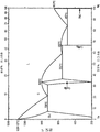
이들의 Cu-Mg 계 합금에서는, 도 1 에 나타내는 Cu-Mg 계 상태도로부터 알 수 있는 바와 같이, Mg 의 함유량이 1.3 mass% 이상 (3.3 원자% 이상) 의 경우, 용체화 처리와 석출 처리를 실시함으로써, Cu 와 Mg 로 이루어지는 금속간 화합물을 석출시킬 수 있다. 즉, 이들의 Cu-Mg 계 합금에 있어서는, 석출 경화에 의해 비교적 높은 도전율과 강도를 갖는 것이 가능해지는 것이다.In these Cu-Mg alloys, as can be seen from the Cu-Mg system state diagram shown in Fig. 1, when the Mg content is 1.3 mass% or more (3.3 atomic% or more), the solution treatment and the precipitation treatment are carried out , An intermetallic compound composed of Cu and Mg can be precipitated. That is, in these Cu-Mg-based alloys, it is possible to have a relatively high conductivity and strength by precipitation hardening.
그러나, 비특허문헌 2 및 특허문헌 1 에 기재된 Cu-Mg 계 합금에서는, 모상 중에 많은 조대한 Cu 와 Mg 를 주성분으로 하는 금속간 화합물이 분산되어 있는 점에서, 굽힘 가공 시에 이들의 금속간 화합물이 기점이 되어 균열 등이 발생하기 쉽기 때문에, 복잡한 형상의 전자·전기 기기용 부품을 성형할 수 없다는 문제가 있었다.However, in the Cu-Mg-based alloy described in Non-Patent Document 2 and Patent Document 1, since intermetallic compounds containing a large amount of coarse Cu and Mg as main components are dispersed in the parent phase, There has been a problem in that it is impossible to mold a complicated electronic / electric device component because cracks or the like are likely to occur at the starting point.
특히, 휴대 전화나 PC 등의 민생품에 사용되는 전자·전기 기기용 부품에 있어서는, 소형화 및 경량화가 요구되고 있고, 강도와 굽힘 가공성을 양립한 전자·전기 기기용 구리 합금이 요구되고 있다. 그러나, 상기 서술한 Cu-Mg 계 합금과 같은 석출 경화형 합금에 있어서는, 석출 경화에 의해 강도 및 내력을 향상시키면 굽힘 가공성이 현저하게 저하되어 버리게 된다. 이 때문에, 박육이고 복잡한 형상의 전자·전기 기기용 부품을 성형할 수는 없었다.Particularly, in parts for electric and electronic devices used in consumer products such as cellular phones and PCs, there is a demand for miniaturization and weight reduction, and copper alloys for electronic and electric devices that combine strength and bending workability are required. However, in the precipitation hardening type alloys such as the Cu-Mg type alloys described above, when the strength and the proof strength are improved by precipitation hardening, the bending workability is remarkably lowered. For this reason, it has not been possible to form a thin and complicated component for electronic and electric devices.
그래서, 특허문헌 2 에는, Cu-Mg 합금을 용체화 후에 급냉함으로써 제작한 Cu-Mg 과포화 고용체의 가공 경화형 구리 합금이 제안되어 있다.Thus, Patent Document 2 proposes a work-hardening type copper alloy of a Cu-Mg supersaturated solid, which is produced by solution-quenching and then quenching the Cu-Mg alloy.
이 Cu-Mg 합금은, 우수한 강도, 도전율, 굽힘성의 밸런스가 우수하고, 상기 서술한 전자·전기 기기용 부품의 소재로서 특히 적합하다.This Cu-Mg alloy is excellent in balance of excellent strength, electric conductivity and bending property, and is particularly suitable as a material of the above-described electronic / electric device parts.
그런데, 최근에는, 전자·전기 기기의 가일층의 경량화에 따라, 이들 전자 기기나 전기 기기 등에 사용되는 커넥터 등의 단자, 릴레이, 리드 프레임 등의 전자·전기 기기용 부품의 박육화 및 미세화가 도모되고 있다. 이 때문에, 전자·전기 기기용 부품의 소재가 되는 전자·전기 기기용 구리 합금 소성 가공재에 있어서는, 종래보다, 판두께를 얇고, 혹은, 선경(線徑)을 가늘게 가공하는 것이 요구되고 있다.In recent years, however, as electronic and electric appliances have been made lighter in weight, parts for electronic and electric appliances such as terminals, relays, and lead frames for connectors used in these electronic appliances and electric appliances have become thinner and finer . For this reason, it is required that the copper alloy sintered material for electric and electronic appliances which is a material of parts for electronic and electric appliances is made thinner in plate thickness or finer in diameter than in the past.
여기서, 전자·전기 기기용 구리 합금의 내부에 산화물 등의 조대한 개재물이 많이 존재하고 있는 경우에는, 이들 개재물 등을 기인으로 한 결함이 발생하여, 제조 수율이 대폭 저하된다는 문제가 있었다. 특히 Mg 는 활성 원소인 점에서, 상기 서술한 Cu-Mg 합금에 있어서는, Mg 를 기인으로 하는 개재물이 발생하기 쉬운 경향이 있고, 가공 시에 결함이 발생하기 쉽다는 문제가 있었다.Here, when a large number of coarse inclusions such as oxides are present in the copper alloy for electronic / electric devices, there is a problem that defects are caused by these inclusions and the like, and the production yield is greatly reduced. Particularly, since Mg is an active element, in the above-described Cu-Mg alloy, inclusions originating from Mg tend to be generated, and there is a problem that defects tend to occur at the time of processing.
이 발명은, 전술한 사정을 감안하여 이루어진 것으로서, 기계적 특성이 우수함과 함께, 판두께를 얇고, 혹은, 선경을 가늘게 가공한 경우여도 결함의 발생을 억제하는 것이 가능한 전자·전기 기기용 구리 합금, 전자·전기 기기용 구리 합금 소성 가공재, 전자·전기 기기용 부품 및 단자를 제공하는 것을 목적으로 한다.The present invention has been made in consideration of the above-described circumstances, and it is an object of the present invention to provide a copper alloy for electronic / electric equipment capable of suppressing the occurrence of defects even when the plate thickness is thin, A copper alloy firing processing material for electronic and electric devices, and a component and a terminal for electronic and electric devices.
이 과제를 해결하기 위해서, 본 발명의 전자·전기 기기용 구리 합금은, Mg 를 1.3 mass% 이상 2.8 mass% 이하의 범위에서 함유하고, 잔부가 실질적으로 Cu 및 불가피 불순물로 되고, H 의 함유량이 10 massppm 이하, O 의 함유량이 100 massppm 이하, S 의 함유량이 50 massppm 이하, C 의 함유량이 10 massppm 이하로 되어 있는 것을 특징으로 하고 있다.In order to solve this problem, the copper alloy for electronic / electric equipment of the present invention contains Mg in a range of 1.3 mass% to 2.8 mass%, the remainder substantially becomes Cu and inevitable impurities, and the content of
상기 서술한 구성으로 된 전자·전기 기기용 구리 합금에 있어서는, O 의 함유량이 100 massppm 이하, S 의 함유량이 50 massppm 이하로 되어 있으므로, Mg 산화물이나 Mg 황화물 등으로 이루어지는 개재물을 저감할 수 있어, 가공 시에 있어서의 결함의 발생을 억제할 수 있다. 또, O 및 S 와 반응함으로써 Mg 가 소비되는 것을 방지할 수 있어, 기계적 특성의 열화를 억제할 수 있다.In the copper alloy for electronic / electric devices having the above-described constitution, since the content of O is 100 mass ppm or less and the content of S is 50 mass ppm or less, inclusions composed of Mg oxide, Mg sulfide and the like can be reduced, It is possible to suppress the occurrence of defects at the time of processing. In addition, Mg can be prevented from being consumed by reacting with O and S, and deterioration of mechanical properties can be suppressed.
또, H 의 함유량이 10 massppm 이하로 되어 있으므로, 주괴 내에 블로우홀 결함이 발생하는 것을 억제할 수 있어, 가공 시에 있어서의 결함의 발생을 억제할 수 있다.In addition, since the content of H is 10 mass ppm or less, it is possible to suppress the occurrence of blowhole defects in the ingot, and it is possible to suppress the occurrence of defects during processing.
또한, C 의 함유량이 10 massppm 이하로 되어 있으므로, 냉간 가공성을 확보 할 수 있어, 가공 시에 있어서의 결함의 발생을 억제할 수 있다.Further, since the content of C is 10 mass ppm or less, the cold workability can be ensured, and the occurrence of defects during processing can be suppressed.
여기서, 본 발명의 전자·전기 기기용 구리 합금에서는, 주사형 전자 현미경 관찰에 있어서, 입경 0.1 ㎛ 이상의 Cu 와 Mg 를 주성분으로 하는 금속간 화합물의 평균 개수가, 1 개/㎛2 이하로 되어 있는 것이 바람직하다.Here, in the copper alloy for electronic / electric apparatus of the present invention, the average number of intermetallic compounds mainly composed of Cu and Mg having a particle diameter of 0.1 탆 or more is 1 / 탆 2 or less in a scanning electron microscopic observation .
이 경우, 도 1 의 상태도에 나타내는 바와 같이, Mg 를 고용 한도 이상의 1.3 mass% 이상 2.8 mass% 이하 (3.3 원자% 이상 6.9 원자% 이하) 의 범위에서 함유하고 있고, 또한, 주사형 전자 현미경 관찰에 있어서, 입경 0.1 ㎛ 이상의 Cu 와 Mg 를 주성분으로 하는 금속간 화합물의 평균 개수가, 1 개/㎛2 이하로 되어 있는 점에서, Cu 와 Mg 를 주성분으로 하는 금속간 화합물의 석출이 억제되어 있고, Mg 가 모상 중에 과포화로 고용된 Cu-Mg 과포화 고용체가 된다.In this case, as shown in the state diagram of Fig. 1, it is contained in a range of 1.3 mass% or more and 2.8 mass% or less (3.3 atomic% or more and 6.9 atomic% or less) , The average number of intermetallic compounds mainly composed of Cu and Mg having a particle diameter of 0.1 占 퐉 or more is 1 / 占 퐉 2 or less. Therefore, precipitation of an intermetallic compound containing Cu and Mg as main components is suppressed, Mg becomes supersaturated Cu-Mg supersaturated solid solution in the mother phase.
또한, 입경 0.1 ㎛ 이상의 Cu 와 Mg 를 주성분으로 하는 금속간 화합물의 평균 개수는, 전계 방출형 주사 전자 현미경을 사용하여, 배율 : 5 만배, 시야 : 약 4.8 ㎛2 에서 10 시야의 관찰을 실시하여 산출한다.The average number of intermetallic compounds containing Cu and Mg as main components having a particle diameter of 0.1 占 퐉 or more was observed at 10 fields of view at a magnification of 50,000 times and a field of view of about 4.8 占 퐉 2 using a field emission scanning electron microscope .
또, Cu 와 Mg 를 주성분으로 하는 금속간 화합물의 입경은, 금속간 화합물의 장경 (도중에 입계에 접하지 않는 조건으로 입자 내에 가장 길게 그을 수 있는 직선의 길이) 과 단경 (장경과 직각으로 교차하는 방향에서, 도중에 입계에 접하지 않는 조건으로 가장 길게 그을 수 있는 직선의 길이) 의 평균치로 한다.The particle diameter of an intermetallic compound containing Cu and Mg as a main component is determined by the relationship between the long diameter of the intermetallic compound (the length of the straightest line that can be drawn the longest in the particle on the condition that it does not touch the grain boundary in the middle) and the short axis The length of the straight line that can be drawn the longest on the condition that it does not touch the grain boundary in the middle).
이와 같은 Cu-Mg 과포화 고용체로 이루어지는 구리 합금에 있어서는, 모상 중에는, 균열의 기점이 되는 조대한 Cu 와 Mg 를 주성분으로 하는 금속간 화합물이 많이 분산되어 있지 않고, 굽힘 가공성이 향상되게 되는 점에서, 복잡한 형상의 커넥터 등의 단자, 릴레이, 리드 프레임 등의 전자·전기 기기용 부품을 성형하는 것이 가능해진다.In the copper alloy made of such a Cu-Mg supersaturated solid solution, since coarse Cu and Mg-based intermetallic compounds which are the origin of cracks are not widely dispersed in the core phase and the bending workability is improved, It becomes possible to form parts for electronic and electric devices such as terminals, relays, and lead frames of connectors having complex shapes.
또한, Mg 를 과포화로 고용시키고 있는 점에서, 가공 경화에 의해 강도를 향상시키는 것이 가능해진다.In addition, since Mg is solubilized by supersaturation, the strength can be improved by work hardening.
또, 본 발명의 전자·전기 기기용 구리 합금에 있어서는, 도전율 σ (%IACS) 가, Mg 의 함유량을 A 원자% 로 했을 때에,In the copper alloy for electric / electronic equipment of the present invention, when the conductivity? (% IACS) and the content of Mg are A atomic%
σ ≤ 1.7241/(-0.0347 × A2 + 0.6569 × A + 1.7) × 100 의 범위 내로 되어 있는 것이 바람직하다.it is preferable that the value is within a range of? 1.7241 / (- 0.0347 x A 2 + 0.6569 x A + 1.7) x 100.
이 경우, 도 1 의 상태도에 나타내는 바와 같이, Mg 를 고용 한도 이상의 Mg 를 1.3 mass% 이상 2.8 mass% 이하 (3.3 원자% 이상 6.9 원자% 이하) 의 범위에서 함유하고 있고, 또한, 도전율이 상기의 범위 내로 되어 있는 점에서, Mg 가 모상 중에 과포화로 고용된 Cu-Mg 과포화 고용체가 된다.In this case, as shown in the state diagram of Fig. 1, Mg contained in the range of 1.3 mass% or more and 2.8 mass% or less (3.3 atomic% or more and 6.9 atomic% or less) , Mg becomes a supersaturated Cu-Mg solid solution in the mother phase.
따라서, 상기 서술한 바와 같이, 모상 중에는, 균열의 기점이 되는 조대한 Cu 와 Mg 를 주성분으로 하는 금속간 화합물이 많이 분산되어 있지 않아, 굽힘 가공성이 향상되게 되는 점에서, 복잡한 형상의 커넥터 등의 단자, 릴레이, 리드 프레임 등의 전자·전기 기기용 부품을 성형하는 것이 가능해진다.Therefore, as described above, since the coarse Cu and the intermetallic compound mainly composed of Mg, which are starting points of the crack, are not dispersed much in the core phase and the bending workability is improved, It is possible to form parts for electronic and electric devices such as terminals, relays, and lead frames.
또한, Mg 를 과포화로 고용시키고 있는 점에서, 가공 경화에 의해 강도를 향상시키는 것이 가능해진다.In addition, since Mg is solubilized by supersaturation, the strength can be improved by work hardening.
또한, Mg 의 원자% 에 대해서는, 불가피 불순물 원소를 무시하고, Cu 와 Mg 및 그 밖의 원소만으로 이루어진다고 가정하여 산출하면 된다.Further, the atomic% of Mg may be calculated on the assumption that the inevitable impurity element is neglected and consists of only Cu and Mg and other elements.
또, 본 발명의 전자·전기 기기용 구리 합금에 있어서는, Sn, Zn, Al, Ni, Si, Mn, Li, Ti, Fe, Co, Cr, Zr, P 중 1 종 또는 2 종 이상을 합계로 0.01 mass% 이상 3.0 mass% 이하의 범위 내에서 함유하고 있어도 된다.In the copper alloy for electronic / electric equipment of the present invention, one or more of Sn, Zn, Al, Ni, Si, Mn, Li, Ti, Fe, Co, Cr, Zr, And may be contained in a range of 0.01 mass% or more and 3.0 mass% or less.
이들의 원소는, Cu-Mg 합금의 강도 등의 특성을 향상시키는 작용 효과를 갖는 점에서, 요구 특성에 따라 적절히 첨가하는 것이 바람직하다. 여기서, 상기 서술한 원소의 첨가량의 합계가 0.01 mass% 미만에서는, 상기 서술한 강도 향상의 작용 효과를 충분히 얻을 수 없다. 한편, 상기 서술한 원소의 첨가량의 합계가 3.0 mass% 를 초과하면 도전율이 크게 저하되게 된다. 그래서, 본 발명에서는, 상기 서술한 원소의 첨가량의 합계를 0.01 mass% 이상 3.0 mass% 이하의 범위 내로 설정하고 있다.These elements are preferably added appropriately according to the required properties in that they have an action and effect of improving the properties such as the strength of the Cu-Mg alloy. Here, when the sum of the amounts of the above-described elements added is less than 0.01 mass%, the effect of the above-described improvement in strength can not be sufficiently obtained. On the other hand, when the total amount of the above-described elements is more than 3.0 mass%, the conductivity is significantly lowered. Therefore, in the present invention, the sum of the amounts of the above-described elements added is set within the range of 0.01 mass% to 3.0 mass%.
또한, 본 발명의 전자·전기 기기용 구리 합금에 있어서는, 0.2 % 내력이 400 MPa 이상의 기계적 특성을 갖는 것이 바람직하다.Further, in the copper alloy for electric and electronic devices of the present invention, it is preferable that the 0.2% proof stress has a mechanical characteristic of 400 MPa or more.
0.2 % 내력이 400 MPa 이상인 경우에는, 용이하게 소성 변형하지 않게 되기 때문에, 커넥터 등의 단자, 릴레이, 리드 프레임 등의 전자 기기용 부품에 특히 적합하다.When the 0.2% proof stress is 400 MPa or more, it is not easily plastic-deformed. Therefore, it is particularly suitable for parts for electronic devices such as terminals, relays, and lead frames of connectors.
또, 본 발명의 전자·전기 기기용 구리 합금에 있어서는, 판 표면에 있어서의 {111}면으로부터의 X 선 회절 강도를 I{111},{200}면으로부터의 X 선 회절 강도를 I{200},{220}면으로부터의 X 선 회절 강도를 I{220},{311}면으로부터의 X 선 회절 강도를 I{311},{220}면으로부터의 X 선 회절 강도의 비율 R{220}을 R{220}= I{220}/(I{111}+ I{200}+ I{220}+ I{311}) 로 한 경우에, R{220}이 0.9 이하로 되어 있는 것이 바람직하다.In the copper alloy for electric / electronic equipments of the present invention, the X-ray diffraction intensity from the {111} plane on the plate surface is I {111}, the X-ray diffraction intensity from the plane {200} is I {200} }, The X-ray diffraction intensity from the {220} plane is I {220}, the X-ray diffraction intensity from the {311} plane is I {311} It is preferable that R {220} is 0.9 or less when R {220} = I {220} / (I {111} + I {200} + I {220} + I {311} .
이 경우, 판 표면에 있어서의{220}면으로부터의 X 선 회절 강도의 비율 R{220}이 0.9 이하로 되어 있는 점에서, 판 표면에 있어서{220}면의 존재가 억제되어 있게 된다. {220}면은, 압연 가공에 의해 형성되기 쉽고, 이{220}면의 비율이 높아지면, 압연 방향에 대해 굽힘의 축을 평행으로 했을 때의 굽힘 가공성이 현저하게 저하되게 된다. 따라서, 이 판 표면에 있어서의{220}면으로부터의 X 선 회절 강도의 비율 R{220}을 0.9 이하로 억제함으로써, 굽힘 가공성을 확보할 수 있고, 내력-굽힘 밸런스를 향상시킬 수 있다.In this case, since the ratio R {220} of the X-ray diffraction intensity from the {220} plane on the surface of the plate is 0.9 or less, the presence of the {220} plane on the plate surface is suppressed. The {220} face is likely to be formed by rolling. If the ratio of {220} face is high, the bending workability when the bending axis is parallel to the rolling direction is remarkably lowered. Therefore, by suppressing the ratio R {220} of the X-ray diffraction intensity from the {220} plane on the surface of the plate to 0.9 or less, the bending workability can be ensured and the strength-bending balance can be improved.
또한, 상기 서술한 전자·전기 기기용 구리 합금에 있어서는, R{220}이 0.3 이상 0.9 이하로 되어 있는 것이 바람직하다.Further, in the above-described copper alloy for electric / electronic equipments, R {220} is preferably 0.3 or more and 0.9 or less.
또한, 본 발명의 전자·전기 기기용 구리 합금에 있어서는, 압연 방향에 대해 평행 방향으로 인장 시험을 실시했을 때의 강도 TS 와, 0.2 % 내력 YS 로부터 산출되는 항복비 YS/TS 가 90 % 를 초과하는 것이 바람직하다.Further, in the copper alloy for electric and electronic equipments of the present invention, the strength TS when the tensile test is performed in the parallel direction with respect to the rolling direction and the yield ratio YS / TS calculated from the 0.2% proof stress YS exceed 90% .
이 경우, 압연 방향에 대해 평행 방향으로 인장 시험을 실시했을 때의 강도 TS 와 0.2 % 내력 YS 로부터 산출되는 항복비 YS/TS 가 90 % 초과로 되어 있는 점에서, 0.2 % 내력 YS 가 강도 TS 에 대해 상대적으로 높아지고 있다. 따라서, 내력-굽힘 밸런스가 향상되고, 압연 방향에 대해 평행 방향에 있어서의 굽힘 가공성이 우수한 것이 된다. 그 때문에, 릴레이나 대형 단자와 같이, 구리 합금 압연판의 압연 방향에 대해 평행 방향으로 굽힘 가공하여, 복잡한 형상으로 성형한 경우여도, 균열 등의 발생을 억제할 수 있다.In this case, since the yield strength YS / TS calculated from the strength TS when the tensile test is performed in the parallel direction with respect to the rolling direction and the 0.2% proof stress YS is more than 90%, the 0.2% proof stress YS Relative to other countries. Therefore, the strength-bending balance is improved and the bending workability in the direction parallel to the rolling direction is excellent. Therefore, it is possible to suppress the occurrence of cracks or the like even when the copper alloy rolled plate is bended in the parallel direction with respect to the rolling direction, such as a relay or a large terminal, even if it is molded into a complicated shape.
상기 서술한 전자·전기 기기용 구리 합금에 있어서는, 평균 결정 입경이 50 ㎛ 이하로 되어 있는 것이 바람직하다.In the above-described copper alloy for electric / electronic equipments, it is preferable that the average crystal grain size is set to 50 μm or less.
결정 입경과 항복비 YS/TS 의 관계를 조사한 결과, 결정 입경을 작게 함으로써 항복비 YS/TS 를 향상하는 것이 가능한 것이 판명되었다. 그리고, 본 발명의 Cu-Mg 계 합금에 있어서는, 평균 결정 입경을 50 ㎛ 이하로 억제함으로써, 상기 서술한 항복비를 크게 향상시켜 90 % 를 초과하도록 할 수 있다.As a result of examining the relationship between the crystal grain size and the yield ratio YS / TS, it has been found that it is possible to improve the yield ratio YS / TS by decreasing the crystal grain size. In the Cu-Mg-based alloy of the present invention, by suppressing the average crystal grain size to 50 탆 or less, the above-described yield ratio can be greatly improved to exceed 90%.
본 발명의 전자·전기 기기용 구리 합금 소성 가공재는, 상기 서술한 전자·전기 기기용 구리 합금으로 이루어지는 구리 소재를 소성 가공함으로써 형성된 것을 특징으로 하고 있다. 또한, 이 명세서에 있어서 소성 가공재란, 어느 제조 공정에 있어서, 소성 가공이 실시된 구리 합금을 말하는 것으로 한다.The copper alloy calcination processing material for electronic / electric equipment of the present invention is formed by plastic working a copper material composed of the above-described copper alloy for electric / electronic equipments. In this specification, the plasticized material refers to a copper alloy subjected to plastic working in any manufacturing process.
이 구성의 구리 합금 소성 가공재에 있어서는, 상기 서술한 바와 같이, 기계적 특성이 우수한 전자·전기 기기용 구리 합금으로 이루어지는 점에서, 전자·전기 기기용 부품의 소재로서 특히 적합하다.As described above, the copper alloy calcination processing material of this construction is particularly suitable as a material for parts for electronic and electric appliances because it is made of a copper alloy for electronic and electric appliances having excellent mechanical properties.
여기서, 본 발명의 전자·전기 기기용 구리 합금 소성 가공재에 있어서는, 상기 구리 소재를 400 ℃ 이상 900 ℃ 이하의 온도로까지 가열함과 함께, 가열된 상기 구리 소재를 60 ℃/min 이상의 냉각 속도로 200 ℃ 이하로까지 냉각시키는 열처리 공정과, 상기 구리 소재를 소성 가공하는 소성 가공 공정을 갖는 제조 방법에 의해 성형된 것이 바람직하다.Here, in the copper alloy calcining material for electronic / electric appliance of the present invention, the copper material is heated to a temperature of 400 ° C or more and 900 ° C or less, and the heated copper material is cooled at a cooling rate of 60 ° C / min or more It is preferable that the copper foil is formed by a heat treatment step of cooling the copper material to 200 DEG C or lower and a production method having a plastic working step of plastic working the copper material.
이 경우, 상기 서술한 조성의 구리 소재를 400 ℃ 이상 900 ℃ 이하의 온도로까지 가열함으로써, Mg 의 용체화를 실시할 수 있다. 또, 가열된 상기 구리 소재를, 60 ℃/min 이상의 냉각 속도로 200 ℃ 이하로까지 냉각시킴으로써, 냉각의 과정에서 금속간 화합물이 석출되는 것을 억제할 수 있어, 구리 소재를 Cu-Mg 과포화 고용체로 하는 것이 가능해진다. 따라서, 모상 중에 조대한 Cu 와 Mg 를 주성분으로 하는 금속간 화합물이 많이 분산되어 있지 않아, 굽힘 가공성이 향상되게 된다.In this case, the solution of Mg can be performed by heating the copper material having the above composition to a temperature of 400 ° C or more and 900 ° C or less. Further, by cooling the heated copper material to 200 DEG C or less at a cooling rate of 60 DEG C / min or more, precipitation of intermetallic compounds during the cooling process can be suppressed and copper material can be suppressed to a Cu-Mg supersaturated solid solution . Therefore, the intermetallic compound mainly composed of coarse Cu and Mg is not dispersed in the mother phase, and the bending workability is improved.
또, 본 발명의 전자·전기 기기용 구리 합금 소성 가공재에 있어서는, 표면에 Sn 도금이 실시되어 있는 구성으로 해도 된다.In the copper alloy firing processing material for electric and electronic devices of the present invention, the surface may be plated with Sn.
본 발명의 전자·전기 기기용 부품은, 상기 서술한 전자·전기 기기용 구리 합금 소성 가공재로 이루어지는 것을 특징으로 하고 있다. 또한, 본 발명에 있어서의 전자·전기 기기용 부품이란, 커넥터 등의 단자, 릴레이, 리드 프레임 등을 포함하는 것이다.The electronic and electric device component of the present invention is characterized by comprising the above-described copper alloy calcining process material for electronic / electric devices. The parts for electric and electronic equipments in the present invention include terminals such as connectors, relays, lead frames, and the like.
또, 본 발명의 단자는, 상기 서술한 전자·전기 기기용 구리 합금 소성 가공재로 이루어지는 것을 특징으로 하고 있다.In addition, the terminal of the present invention is characterized by being made of the above-described copper alloy calcining material for electronic / electric appliance.
이 구성의 전자·전기 기기용 부품 및 단자는, 기계적 특성이 우수한 전자·전기 기기용 구리 합금 소성 가공재를 사용하여 제조되어 있으므로, 복잡한 형상이어도 균열 등이 발생하지 않고, 신뢰성이 향상되게 된다.The parts and terminals for electronic and electric appliances having this structure are manufactured by using a copper alloy calcining material for electronic and electric appliances having excellent mechanical properties, so that cracks and the like do not occur even in a complicated shape, and reliability is improved.
본 발명에 의하면, 기계적 특성이 우수함과 함께, 판두께를 얇고, 혹은, 선경을 가늘게 가공한 경우여도 결함의 발생을 억제하는 것이 가능한 전자·전기 기기용 구리 합금, 전자·전기 기기용 구리 합금 소성 가공재, 전자·전기 기기용 부품 및 단자를 제공할 수 있다.Industrial Applicability According to the present invention, it is possible to provide a copper alloy for electronic and electric devices, a copper alloy for electronic and electric devices, Machining materials, parts for electronic and electric devices, and terminals.
도 1 은, Cu-Mg 계 상태도이다.
도 2 는, 본 발명의 제 1 실시형태인 전자·전기 기기용 구리 합금의 제조 방법의 플로우도이다.
도 3 은, 본 발명의 제 2 실시형태인 전자·전기 기기용 구리 합금의 제조 방법의 플로우도이다.
도 4 는, 본 발명의 제 3 실시형태인 전자·전기 기기용 구리 합금의 제조 방법의 플로우도이다.1 is a Cu-Mg system state diagram.
Fig. 2 is a flow chart of a method for producing a copper alloy for electronic / electric devices according to a first embodiment of the present invention.
Fig. 3 is a flow chart of a method for producing a copper alloy for electronic / electric devices according to a second embodiment of the present invention.
Fig. 4 is a flowchart of a method for producing a copper alloy for electronic / electric devices according to a third embodiment of the present invention.
이하에, 본 발명의 실시형태에 대해 도면을 참조하여 설명한다.Hereinafter, embodiments of the present invention will be described with reference to the drawings.
(제 1 실시형태)(First Embodiment)
본 실시 형태인 전자·전기 기기용 구리 합금의 성분 조성은, Mg 를 1.3 mass% 이상 2.8 mass% 이하의 범위에서 함유하고, 잔부가 실질적으로 Cu 및 불가피 불순물로 되어 있어, 이른바 Cu-Mg 의 2 원계 합금으로 되어 있다.The composition of the copper alloy for electric and electronic devices according to the present embodiment contains Mg in a range of 1.3 mass% to 2.8 mass%, the remainder being substantially Cu and inevitable impurities, so-called Cu-Mg 2 It is made of a copper alloy.
또, 본 실시 형태인 전자·전기 기기용 구리 합금에 있어서는, 0.2 % 내력이 400 MPa 이상으로 되어 있다.In the case of the copper alloy for electric and electronic devices according to the present embodiment, the 0.2% proof stress is 400 MPa or more.
여기서, 도전율 σ (% IACS) 가, Mg 의 함유량을 A 원자 % 로 했을 때에,σ ≤ 1.7241/(-0.0347 × A2 + 0.6569 × A + 1.7) × 100 의 범위 내로 되어 있다.Here, the conductivity σ (% IACS) is, when the amount of Mg atom by A%, σ ≤ 1.7241 / - is in the range of (0.0347 × A 2 + 0.6569 × A + 1.7) × 100.
또, 주사형 전자 현미경 관찰에 있어서, 입경 0.1 ㎛ 이상의 Cu 와 Mg 를 주성분으로 하는 금속간 화합물의 평균 개수가, 1 개/㎛2 이하로 되어 있다.In addition, in the scanning electron microscopic observation, the average number of intermetallic compounds containing Cu and Mg as main components having a particle diameter of 0.1 占 퐉 or more is 1 / 占 퐉 2 or less.
즉, 본 실시 형태인 전자·전기 기기용 구리 합금은, Cu 와 Mg 를 주성분으로 하는 금속간 화합물이 거의 석출되어 있지 않고, Mg 가 모상 중에 고용 한도 이상으로 고용된 Cu-Mg 과포화 고용체로 되어 있는 것이다.That is, the copper alloy for electronic / electric devices according to the present embodiment is a Cu-Mg supersaturated solid solution in which almost no intermetallic compound containing Cu and Mg as main components is precipitated and Mg is solubilized in a solid phase or more will be.
그리고, 본 실시 형태인 전자·전기 기기용 구리 합금에 있어서는, 불순물 원소인 H, O, S, C 의 함유량이 이하와 같이 정해져 있다.In the copper alloy for electric and electronic devices according to the present embodiment, the contents of H, O, S and C, which are impurity elements, are determined as follows.
H : 10 massppm 이하 H: 10 mass ppm or less
O : 100 massppm 이하 O: 100 mass ppm or less
S : 50 massppm 이하 S: 50 mass ppm or less
C : 10 massppm 이하C: 10 mass ppm or less
여기서, 상기 서술한 바와 같이 성분 조성, 도전율, 석출물의 개수를 규정한 이유에 대해 이하에 설명한다.Here, the reason why the composition, the conductivity, and the number of precipitates are defined as described above will be described below.
(Mg : 1.3 mass% 이상 2.8 mass% 이하) (Mg: 1.3 mass% or more and 2.8 mass% or less)
Mg 는, 도전율을 크게 저하시키지 않고, 강도를 향상시킴과 함께 재결정 온도를 상승시키는 작용 효과를 갖는 원소이다. 또, Mg 를 모상 중에 고용시킴으로써, 우수한 굽힘 가공성이 얻어진다.Mg is an element having an action effect of improving the strength and raising the recrystallization temperature without significantly lowering the conductivity. In addition, when Mg is dissolved in the mother phase, excellent bending workability is obtained.
여기서, Mg 의 함유량이 1.3 mass% 미만에서는, 그 작용 효과를 발휘시킬 수는 없다. 한편, Mg 의 함유량이 2.8 mass% 를 초과하면, 용체화 때문에 열처리를 실시했을 때에, Cu 와 Mg 를 주성분으로 하는 금속간 화합물이 잔존하게 되어, 그 후의 열간 가공 및 냉간 가공 시에 균열이 발생해 버릴 우려가 있다. 이와 같은 이유에서, Mg 의 함유량을, 1.3 mass% 이상 2.8 mass% 이하 (3.3 원자% 이상 6.9 원자% 이하) 로 설정하고 있다.Here, when the content of Mg is less than 1.3 mass%, its action and effect can not be exerted. On the other hand, when the content of Mg exceeds 2.8 mass%, intermetallic compounds containing Cu and Mg as main components remain at the time of heat treatment for solution formation, and cracks are generated during the subsequent hot working and cold working There is a risk of discarding. For this reason, the content of Mg is set to 1.3 mass% or more and 2.8 mass% or less (3.3 atom% or more and 6.9 atom% or less).
또한, Mg 의 함유량이 적으면 강도가 충분히 향상되지 않는다. 또, Mg 는 활성 원소인 점에서, 과잉으로 첨가됨으로써, 용해 주조 시에, 산소와 반응하여 생성된 Mg 산화물이 말려들 우려가 있다. 따라서, Mg 의 함유량을, 1.4 mass% 이상 2.6 mass% 이하 (3.6 원자% 이상 6.5 원자% 이하) 의 범위로 하는 것이, 더욱 바람직하다.When the content of Mg is small, the strength is not sufficiently improved. Further, since Mg is an active element, it is excessively added, so that Mg oxide produced by reaction with oxygen during molten casting may be entangled. Therefore, it is more preferable that the content of Mg is in the range of 1.4 mass% to 2.6 mass% (3.6 atomic% to 6.5 atomic%).
여기서, 상기 서술한 원자% 의 조성치에 대해서는, 본 실시 형태에서는 Cu 와 Mg 의 2 원계 합금으로 되어 있는 점에서, 불가피 불순물 원소를 무시하여 Cu 와 Mg 만으로 이루어진다고 가정하고, mass% 의 값으로부터 산출한 것이다.Here, the compositional value of the above-described atomic% is assumed to be composed of only Cu and Mg by ignoring the inevitable impurity element in the present embodiment because it is a binary alloy of Cu and Mg in this embodiment, Respectively.
(H (수소) : 10 massppm 이하) (H (hydrogen): 10 mass ppm or less)
H 는, 주조 시에 O 와 결부되어 수증기가 되고, 주괴 중에 블로우홀 결함을 발생시키는 원소이다. 이 블로우홀 결함은, 주조 시에는 균열, 압연 시에는 팽창 및 박리 등의 결함의 원인이 된다. 이들의 균열, 팽창 및 박리 등의 결함은, 응력 집중하여 파괴의 기점이 되기 때문에, 강도, 내응력 부식 균열 특성을 열화시키는 것이 알려져 있다. 여기서, H 의 함유량이 10 massppm 을 초과하면, 상기 서술한 블로우홀 결함이 발생하기 쉬워진다.H is an element that forms water vapor in association with O at the time of casting and causes a blowhole defect in the ingot. This blowhole defect is a cause of defects such as cracking during casting and expansion and peeling during rolling. It is known that defects such as cracks, expansion, peeling, and the like are caused by stress concentration and become a starting point of fracture, thereby deteriorating strength and stress corrosion cracking characteristics. Here, when the content of H exceeds 10 mass ppm, the aforementioned blowhole defect tends to occur.
그래서, 본 실시 형태에서는, H 의 함유량을 10 massppm 이하로 규정하고 있다. 또한, 블로우홀 결함의 발생을 한층 더 억제하기 위해서는, H 의 함유량을 4 massppm 이하로 하는 것이 바람직하고, 2 massppm 이하로 하는 것이 더욱 바람직하다. 상기 서술한 전자·전기 기기용 구리 합금의 얻어지는 효과를 고려하면, 바람직한 상기 H 의 함유량의 하한치는 0.01 massppm 이지만, 이것으로 한정되는 일은 없다.Thus, in the present embodiment, the content of H is specified to be 10 mass ppm or less. In order to further suppress the occurrence of blowhole defects, the content of H is preferably 4 mass ppm or less, and more preferably 2 mass ppm or less. Considering the effect obtained by the above-described copper alloy for electric / electronic equipments, the lower limit of the content of H is preferably 0.01 mass ppm, but the present invention is not limited thereto.
(O (산소) : 100 massppm 이하) (O (oxygen): 100 mass ppm or less)
O 는, 구리 합금 중의 각 성분 원소와 반응하여 산화물을 형성하는 원소이다. 이들의 산화물은, 파괴의 기점이 되기 때문에, 냉간 압연성이 저하되고, 또한 굽힘 가공성도 나빠진다. 또, O 가 100 massppm 을 초과한 경우에는, Mg 와 반응함으로써, Mg 가 소비되어 버려, Cu 의 모상 중에 대한 Mg 의 고용량이 저감되어, 기계적 특성이 열화될 우려가 있다.O is an element that reacts with each component element in the copper alloy to form an oxide. These oxides are the starting point of fracture, so that the cold rolling property is deteriorated and the bending workability is also deteriorated. On the other hand, when O exceeds 100 mass ppm, Mg is consumed by reacting with Mg, and there is a fear that the amount of Mg contained in the mother phase of Cu is reduced and mechanical properties are deteriorated.
그래서, 본 실시 형태에서는, O 의 함유량을 100 massppm 이하로 규정하고 있다. 또한, O 의 함유량은, 상기의 범위 내에서도 특히 50 massppm 이하가 바람직하고, 20 massppm 이하가 더욱 바람직하다. 상기 서술한 전자·전기 기기용 구리 합금의 얻어지는 효과를 고려하면, 바람직한 상기 O 의 함유량의 하한치는 0.01 massppm 이지만, 이것으로 한정되는 일은 없다.Thus, in this embodiment, the content of O is specified to be 100 mass ppm or less. Also, the content of O is preferably 50 mass ppm or less, more preferably 20 mass ppm or less, even within the above range. Considering the effect obtained by the above-described copper alloy for electric / electronic devices, the lower limit of the content of O is preferably 0.01 mass ppm, but the present invention is not limited thereto.
(S (황) : 50 massppm 이하) (S (sulfur): 50 mass ppm or less)
S 는 금속간 화합물 또는 복합 황화물 등의 형태로 결정립계에 존재하는 원소이다. 이들의 입계에 존재하는 금속간 화합물 또는 복합 황화물은, 열간 가공 시에 입계 균열을 일으켜, 가공 균열의 원인이 된다. 또, 이들은 파괴의 기점이 되기 때문에, 냉간 압연성이나 굽힘 가공성이 열화된다. 또한, Mg 와 반응함으로써, Mg 가 소비되어 버려, Cu 의 모상 중에 대한 Mg 의 고용량이 저감되어, 기계적 특성이 열화될 우려가 있다.S is an element present in the grain boundary in the form of an intermetallic compound or complex sulfide. Intermetallic compounds or complex sulfides present in the grain boundaries cause intergranular cracks during hot working, and cause cracks in the work. In addition, since these become the starting point of fracture, the cold rolling property and the bending workability are deteriorated. Further, by reacting with Mg, Mg is consumed, and there is a fear that the amount of Mg dissolved in the core phase of Cu is reduced, and the mechanical properties are deteriorated.
그래서, 본 실시 형태에서는, S 의 함유량을 50 massppm 이하로 규정하고 있다. 또한, S 의 함유량은, 상기의 범위 내에서도 특히 40 massppm 이하가 바람직하고, 30 massppm 이하가 더욱 바람직하다. 상기 서술한 전자·전기 기기용 구리 합금의 얻어지는 효과를 고려하면, 바람직한 상기의 하한치 S 의 함유량은 0.01 massppm 이지만, 이것으로 한정되는 일은 없다.Thus, in the present embodiment, the content of S is specified to be 50 mass ppm or less. The content of S is particularly preferably 40 mass ppm or less, more preferably 30 mass ppm or less, even within the above range. Considering the effect obtained by the above-described copper alloy for electric / electronic equipment, the content of the lower limit value S is preferably 0.01 mass ppm, but the present invention is not limited thereto.
(C (탄소) : 10 massppm 이하) (C (carbon): 10 mass ppm or less)
C 는, 용탕(溶湯)의 탈산 작용을 목적으로 하여, 용해, 주조에 있어서 용탕 표면을 피복하도록 사용되는 것이며, 불가피적으로 혼입될 우려가 있는 원소이다. C 의 함유량이 10 massppm 을 초과하면, 주조 시의 C 의 말려듦이 많아진다. 이들의 C 나 복합 탄화물, C 의 고용체의 편석은 냉간 압연성을 열화시킨다.C is used to coat the surface of the molten metal in dissolution and casting for the purpose of deoxidizing the molten metal and is an element that may inevitably be incorporated. If the content of C exceeds 10 mass ppm, the amount of C during casting increases. The segregation of these solid solutions of C, complex carbides, and C deteriorates the cold rolling resistance.
그래서, 본 실시 형태에서는, C 의 함유량을 10 massppm 이하로 규정하고 있다. 또한, C 의 함유량은, 상기의 범위 내에서도 5 massppm 이하가 바람직하고, 1 massppm 이하가 더욱 바람직하다.Therefore, in this embodiment, the content of C is specified to be 10 mass ppm or less. The content of C is preferably 5 mass ppm or less, more preferably 1 mass ppm or less, even within the above range.
그 밖의 불가피 불순물로서는, Ag, B, Ca, Sr, Ba, Sc, Y, 희토류 원소, Hf, V, Nb, Ta, Mo, W, Re, Ru, Os, Se, Te, Rh, Ir, Pd, Pt, Au, Cd, Ga, In, Ge, As, Sb, Tl, Pb, Bi, Be, N, Hg 등을 들 수 있다. 이들의 불가피 불순물은, 총량으로 0.3 mass% 이하인 것이 바람직하다.As other inevitable impurities, Ag, B, Ca, Sr, Ba, Sc, Y, a rare earth element, Hf, V, Nb, Ta, Mo, W, Re, Ru, Os, Se, , Pt, Au, Cd, Ga, In, Ge, As, Sb, Tl, Pb, Bi, Be, N and Hg. These inevitable impurities are preferably 0.3 mass% or less in total.
(도전율 σ (% IACS))(Conductivity? (% IACS))
Cu 와 Mg 의 2 원계 합금에 있어서, 도전율 σ (% IACS) 가, Mg 의 함유량을 A 원자% 로 했을 때에,When the conductivity? (% IACS) and the Mg content is A atomic% in a binary alloy of Cu and Mg,
σ ≤ 1.7241/(-0.0347 × A2 + 0.6569 × A + 1.7) × 100 의 범위 내인 경우에는, 금속간 화합물이 거의 존재하지 않게 된다.In the case of σ ≦ 1.7241 / (- 0.0347 × A 2 + 0.6569 × A + 1.7) × 100, almost no intermetallic compound is present.
즉, 도전율 σ (% IACS) 가 상기 식을 초과하는 경우에는, 금속간 화합물이 다량으로 존재하고, 사이즈도 비교적 큰 점에서, 굽힘 가공성이 대폭 열화하게 된다. 따라서, 도전율 σ (% IACS) 가, 상기 식의 범위 내가 되도록, 제조 조건을 조정한다.That is, when the conductivity? (% IACS) exceeds the above formula, the intermetallic compound exists in a large amount and the size is relatively large, so that the bending workability is greatly deteriorated. Therefore, the manufacturing conditions are adjusted so that the conductivity? (% IACS) is within the range of the above formula.
또한, 상기 서술한 작용 효과를 확실하게 발휘시키기 위해서는, 도전율 σ (% IACS) 를,In order to reliably exhibit the above-described action and effect, the conductivity? (% IACS)
σ ≤ 1.7241/(-0.0292 × A2 + 0.6797 × A + 1.7) × 100 의 범위 내로 하는 것이 바람직하다. 이 경우, Cu 와 Mg 를 주성분으로 하는 금속간 화합물이 보다 소량이기 때문에, 굽힘 가공성이 한층 더 향상되게 된다.it is preferable that the value is within a range of? 1.7241 / (- 0.0292 x A 2 + 0.6797 x A + 1.7) x 100. In this case, since the amount of the intermetallic compound containing Cu and Mg as a main component is smaller, the bending workability is further improved.
(석출물)(Precipitate)
본 실시 형태인 전자·전기 기기용 구리 합금에 있어서는, 주사형 전자 현미경으로 관찰한 결과, 입경 0.1 ㎛ 이상의 Cu 와 Mg 를 주성분으로 하는 금속간 화합물의 평균 개수가, 1 개/㎛2 이하로 되어 있다. 즉, Cu 와 Mg 를 주성분으로 하는 금속간 화합물이 거의 석출되어 있지 않고, Mg 가 모상 중에 고용되어 있는 것이다.In the case of the copper alloy for electric and electronic devices according to the present embodiment, observation by a scanning electron microscope revealed that the average number of intermetallic compounds containing Cu and Mg as main components having a particle diameter of 0.1 탆 or more was 1 / 탆 2 or less have. That is, almost no intermetallic compound containing Cu and Mg as main components is precipitated, and Mg is dissolved in the mother phase.
여기서, 용체화가 불완전하거나 용체화 후에 Cu 와 Mg 를 주성분으로 하는 금속간 화합물이 석출함으로써, 사이즈가 큰 금속간 화합물이 다량으로 존재하면, 이들의 금속간 화합물이 균열의 기점이 되어, 굽힘 가공성이 대폭 열화하게 된다.Here, if the solvation is incomplete or after the solution is formed, an intermetallic compound mainly composed of Cu and Mg is precipitated, and if a large amount of large intermetallic compound is present, these intermetallic compounds become a starting point of cracking and bending workability This is greatly deteriorated.
조직을 조사한 결과, 입경 0.1 ㎛ 이상의 Cu 와 Mg 를 주성분으로 하는 금속간 화합물이 합금 중에 1 개/㎛2 이하의 경우, 즉, Cu 와 Mg 를 주성분으로 하는 금속간 화합물이 존재하지 않거나 혹은 소량인 경우, 양호한 굽힘 가공성이 얻어지게 된다.As a result of investigation of the structure, it was found that when the intermetallic compound containing Cu and Mg as main components having a particle size of 0.1 탆 or more is not more than 1 / 탆 2 in the alloy, that is, the intermetallic compound containing Cu and Mg as main components is not present, , Good bending workability can be obtained.
또한, 상기 서술한 작용 효과를 확실하게 발휘시키기 위해서는, 입경 0.05 ㎛ 이상의 Cu 와 Mg 를 주성분으로 하는 금속간 화합물의 개수가 합금 중에 1 개/㎛2 이하인 것이, 보다 바람직하다.It is more preferable that the number of intermetallic compounds containing Cu and Mg as main components of not less than 0.05 mu m and not more than 1 / mu m 2 in the alloy is more preferable in order to reliably exhibit the above-described action and effect.
또한, Cu 와 Mg 를 주성분으로 하는 금속간 화합물의 평균 개수는, 전계 방출형 주사 전자 현미경을 사용하여, 배율 : 5 만배, 시야 : 약 4.8 ㎛2 에서 10 시야의 관찰을 실시하고, 그 평균치를 산출한다.The average number of intermetallic compounds containing Cu and Mg as a main component was observed with a Field Emission Scanning Electron Microscope at a magnification of 50,000 times and a field of view of about 4.8 占 퐉 2 at 10 fields of view, .
또, Cu 와 Mg 를 주성분으로 하는 금속간 화합물의 입경은, 금속간 화합물의 장경 (도중에 입계에 접하지 않는 조건으로 입자 내에 가장 길게 그을 수 있는 직선의 길이) 과 단경 (장경과 직각으로 교차하는 방향에서, 도중에 입계에 접하지 않는 조건으로 가장 길게 그을 수 있는 직선의 길이) 의 평균치로 한다.The particle diameter of an intermetallic compound containing Cu and Mg as a main component is determined by the relationship between the long diameter of the intermetallic compound (the length of the straightest line that can be drawn the longest in the particle on the condition that it does not touch the grain boundary in the middle) and the short axis The length of the straight line that can be drawn the longest on the condition that it does not touch the grain boundary in the middle).
여기서, Cu 와 Mg 를 주성분으로 하는 금속간 화합물은, 화학식 MgCu2, 프로토타입 MgCu2, 피어슨 기호 cF24, 공간군 번호 Fd-3m 으로 나타내는 결정 구조를 갖는 것이다.Here, the intermetallic compound mainly composed of Cu and Mg has a crystal structure represented by the formula MgCu 2 , prototype MgCu 2 , Pearson symbol cF24 and space group number Fd-3m.
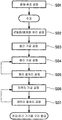
다음으로, 이와 같은 구성으로 된 본 실시 형태인 전자·전기 기기용 구리 합금의 제조 방법 및 전자·전기 기기용 구리 합금 소성 가공재의 제조 방법에 대해, 도 2 에 나타내는 플로우도를 참조하여 설명한다.Next, a method of manufacturing a copper alloy for electronic and electric apparatuses and a method of producing a copper alloy sintered processing material for electronic / electrical equipments according to this embodiment having such a structure will be described with reference to a flow chart shown in Fig.
(용해·주조 공정 S01)(Melting and casting step S01)
먼저, 구리 원료를 용해하여 얻어진 구리 용탕에, 전술한 원소를 첨가하여 성분 조정을 실시하고, 구리 합금 용탕을 제출한다. 또한, Mg 의 첨가에는, Mg 단체나 Cu-Mg 모합금 등을 사용할 수 있다. 또, Mg 를 함유하는 원료를 구리 원료와 함께 용해해도 된다. 또, 본 합금의 리사이클재 및 스크랩재를 사용해도 된다.First, the above-mentioned element is added to the copper melt obtained by dissolving the copper raw material, and the composition adjustment is performed, and the copper alloy melt is submitted. For Mg addition, Mg group, Cu-Mg parent alloy and the like can be used. In addition, the Mg-containing raw material may be dissolved together with the copper raw material. It is also possible to use recycled materials and scrap materials of this alloy.
여기서, 구리 용탕은, 순도가 99.99 질량% 이상으로 된 이른바 4NCu 로 하는 것이 바람직하다. 특히, 본 실시 형태에서는, H, O, S, C 의 함유량을 상기 서술한 바와 같이 규정하고 있는 점에서, 이들의 원소의 함유량의 적은 원료를 선별하여 사용하게 된다. 또, 용해 공정에서는, Mg 의 산화를 억제하기 위해서, 진공로, 혹은, 불활성 가스 분위기 또는 환원성 분위기로 된 분위기로를 사용하는 것이 바람직하다.Here, the molten copper is preferably so-called 4 NCu having a purity of 99.99 mass% or more. Particularly, in this embodiment, since the contents of H, O, S, and C are specified as described above, raw materials having a small content of these elements are selected and used. In the dissolving step, in order to suppress the oxidation of Mg, it is preferable to use a vacuum furnace, or an atmosphere of an inert gas atmosphere or a reducing atmosphere.
그리고, 성분 조정된 구리 합금 용탕을 주형에 주입하여 주괴를 제출한다. 또한, 양산을 고려한 경우에는, 연속 주조법 또는 반연속 주조법을 사용하는 것이 바람직하다.Then, the molten copper alloy is injected into the mold and the ingot is submitted. When mass production is considered, it is preferable to use a continuous casting method or a semi-continuous casting method.
(균질화/용체화 공정 S02)(Homogenization / solution processing step S02)
다음으로, 얻어진 주괴의 균질화 및 용체화를 위해서 가열 처리를 실시한다. 주괴의 내부에는, 응고의 과정에 있어서 Mg 가 편석으로 농축됨으로써 발생한 Cu 와 Mg 를 주성분으로 하는 금속간 화합물 등이 존재하게 된다. 그래서, 이들의 편석 및 금속간 화합물 등을 소실 또는 저감시키기 위해서, 주괴를 400 ℃ 이상 900 ℃ 이하로까지 가열하는 가열 처리를 실시함으로써, 주괴 내에 있어서, Mg 를 균질로 확산시키거나, Mg 를 모상 중에 고용시키거나 하는 것이다. 또한, 이 균질화/용체화 공정 S02 는, 비산화성 또는 환원성 분위기 중에서 실시하는 것이 바람직하다. 또, 400 ℃ 이상 900 ℃ 이하로까지 가열된 구리 소재를, 200 ℃ 이하의 온도로까지, 60℃/min 이상의 냉각 속도로 냉각시킨다.Next, heat treatment is performed to homogenize and solidify the obtained ingot. Inside the ingot, an intermetallic compound mainly composed of Cu and Mg, which is formed by concentrating Mg into segregation in the solidification process, exists. Therefore, in order to eliminate or reduce segregation and intermetallic compounds of these, it is possible to homogeneously diffuse Mg in the ingot by performing heat treatment for heating the ingot to 400 ° C or more and 900 ° C or less, Or to hire them. Further, the homogenization / solubilization step S02 is preferably carried out in a non-oxidizing or reducing atmosphere. Further, the copper material heated to 400 ° C or more and 900 ° C or less is cooled to a temperature of 200 ° C or less at a cooling rate of 60 ° C / min or more.
여기서, 가열 온도가 400 ℃ 미만에서는, 용체화가 불완전해져, 모상 중에 Cu 와 Mg 를 주성분으로 하는 금속간 화합물이 많이 잔존할 우려가 있다. 한편, 가열 온도가 900 ℃ 를 초과하면, 구리 소재의 일부가 액상이 되어, 조직이나 표면 상태가 불균일해질 우려가 있다. 따라서, 가열 온도를 400 ℃ 이상 900 ℃ 이하의 범위로 설정하고 있다. 보다 바람직하게는 500 ℃ 이상 850 ℃ 이하, 더욱 바람직하게는 520 ℃ 이상 800 ℃ 이하로 한다.If the heating temperature is lower than 400 占 폚, solution conversion becomes incomplete and there is a possibility that a large amount of intermetallic compounds containing Cu and Mg as main components remain in the mother phase. On the other hand, if the heating temperature exceeds 900 占 폚, a part of the copper material becomes a liquid phase, and there is a fear that the texture and the surface state become uneven. Therefore, the heating temperature is set in the range of 400 DEG C or more and 900 DEG C or less. More preferably 500 ° C or more and 850 ° C or less, and further preferably 520 ° C or more and 800 ° C or less.
(열간 가공 공정 S03)(Hot working step S03)
조가공의 효율화와 조직의 균일화를 위해서, 열간 가공을 실시해도 된다. 이 열간 가공 공정 S03 에 있어서의 온도 조건은 특별히 한정은 없지만, 400 ℃ 내지 900 ℃ 의 범위 내로 하는 것이 바람직하다. 또, 가공 후의 냉각 방법은, 물 퀀칭 등 60 ℃/min 이상의 냉각 속도로 200 ℃ 이하로까지 냉각시키는 것이 바람직하다. 또한, 가공 방법에 대해서는, 특별히 한정은 없고, 예를 들어 압연, 선긋기, 압출, 홈 압연, 단조, 프레스 등을 채용할 수 있다.Hot working may be performed to improve the efficiency of coarse processing and uniformity of the structure. The temperature condition in the hot working step S03 is not particularly limited, but it is preferably within the range of 400 占 폚 to 900 占 폚. It is preferable that the cooling method after processing is carried out at a cooling rate of not less than 200 캜 at a cooling rate of not less than 60 캜 / min such as water quenching. The processing method is not particularly limited, and for example, rolling, line drawing, extrusion, grooving, forging, pressing and the like can be adopted.
(중간 가공 공정 S04)(Intermediate processing step S04)
다음으로, 구리 소재를 필요에 따라 절단함과 함께, 표면에 생성된 산화막 등을 제거하기 위해서 필요에 따라 표면 연삭을 실시한다. 그리고, 소정의 형상으로 소성 가공을 실시한다.Next, the copper material is cut as necessary, and surface grinding is performed as necessary to remove the oxide film and the like formed on the surface. Then, plastic working is performed in a predetermined shape.
또한, 이 중간 가공 공정 S04 에 있어서의 온도 조건은 특별히 한정은 없지만, 냉간 또는 온간 가공이 되는 -200 ℃ 내지 200 ℃ 의 범위 내로 하는 것이 바람직하다. 또, 가공율은, 최종 형상에 근사하도록 적절히 선택되게 되지만, 최종 형상을 얻기까지의 중간 열처리 공정 S05 의 횟수를 줄이기 위해서는, 20 % 이상으로 하는 것이 바람직하다. 또, 가공율을 30 % 이상으로 하는 것이 보다 바람직하다. 소성 가공 방법은 특별히 한정되지 않지만, 예를 들어 압연, 선긋기, 압출, 홈 압연, 단조, 프레스 등을 채용할 수 있다. 상기 서술한 전자·전기 기기용 구리 합금 소성 가공재의 얻어지는 효과를 고려하면, 바람직한 상기 가공율의 상한치는 99 % 이지만, 이것으로 한정되는 일은 없다.The temperature condition in this intermediate processing step S04 is not particularly limited, but is preferably set within the range of -200 DEG C to 200 DEG C for cold or warm working. The machining rate is appropriately selected so as to approximate the final shape. However, in order to reduce the number of intermediate heat treatment steps S05 until the final shape is obtained, the machining rate is preferably 20% or more. In addition, it is more preferable to set the processing rate to 30% or more. The plastic working method is not particularly limited, and for example, rolling, line drawing, extrusion, grooving, forging, pressing and the like can be adopted. Considering the effect obtained by the above-described copper alloy calcining material for electric / electronic equipment, the upper limit value of the above-mentioned processing rate is preferably 99%, but is not limited thereto.
(중간 열처리 공정 S05)(Intermediate heat treatment step S05)
중간 가공 공정 S04 후에, 용체화의 철저, 재결정 조직화 또는 가공성 향상을 위한 연화를 목적으로 하여 열처리를 실시한다.After the intermediate processing step S04, heat treatment is carried out for the purpose of thoroughly solvating, softening for recrystallization, or improving workability.
열처리의 방법은 특별히 한정은 없지만, 바람직하게는 400 ℃ 이상 900 ℃ 이하의 조건에서, 비산화 분위기 또는 환원성 분위기 중에서 열처리를 실시한다. 보다 바람직하게는 400 ℃ 이상 850 ℃ 이하, 더욱 바람직하게는 520 ℃ 이상 800 ℃ 이하로 한다.The method of the heat treatment is not particularly limited, but preferably heat treatment is performed in a non-oxidizing atmosphere or a reducing atmosphere at a temperature of 400 占 폚 to 900 占 폚. More preferably 400 ° C or more and 850 ° C or less, and still more preferably 520 ° C or more and 800 ° C or less.
또한, 중간 가공 공정 S04 및 중간 열처리 공정 S05 는, 반복하여 실시해도 된다.The intermediate processing step S04 and the intermediate heat treatment step S05 may be repeated.
여기서, 중간 열처리 공정 S05 에 있어서는, 400 ℃ 이상 900 ℃ 이하로까지 가열된 구리 소재를, 200 ℃ 이하의 온도로까지, 60 ℃/min 의 냉각 속도로 냉각시키는 것이 바람직하다. 이와 같이 급냉함으로써, 모상 중에 고용된 Mg 가 Cu 와 Mg 를 주성분으로 하는 금속간 화합물로서 석출되는 것이 억제되게 되어, 구리 소재를 Cu-Mg 과포화 고용체로 할 수 있다.Here, in the intermediate heat treatment step S05, it is preferable that the copper material heated to 400 DEG C or more and 900 DEG C or less is cooled to a temperature of 200 DEG C or less at a cooling rate of 60 DEG C / min. By such rapid cooling, precipitation of Mg dissolved in the mother phase as an intermetallic compound mainly composed of Cu and Mg is suppressed, and the copper material can be made into a Cu-Mg supersaturated solid solution.
(마무리 가공 공정 S06)(Finishing step S06)
중간 열처리 공정 S05 후의 구리 소재를 소정의 형상으로 마무리 가공을 실시한다. 또한, 이 마무리 가공 공정 S06 에 있어서의 온도 조건은 특별히 한정은 없지만, 상온에서 실시하는 것이 바람직하다. 또, 가공율은, 최종 형상에 근사하도록 적절히 선택되게 되지만, 가공 경화에 의해 강도를 향상시키기 위해서는, 20 % 이상으로 하는 것이 바람직하다. 또 가일층의 강도의 향상을 도모하는 경우에는, 가공율을 30 % 이상으로 하는 것이 보다 바람직하다. 여기서, 가공 방법으로 특별히 한정은 없고, 예를 들어 최종 형태가 판이나 조의 경우에는 압연, 선이나 봉의 경우에는 선긋기나 압출이나 홈 압연 등, 벌크 형상의 경우에는 단조나 프레스를 채용할 수 있다.The copper material after the intermediate heat treatment step S05 is finished in a predetermined shape. The temperature condition in this finishing step S06 is not particularly limited, but is preferably carried out at room temperature. The machining rate is appropriately selected so as to approximate the final shape, but in order to improve the strength by work hardening, the machining rate is preferably 20% or more. In addition, when the strength of the farthest layer is to be improved, it is more preferable to set the machining ratio to 30% or more. Here, the working method is not particularly limited, and for example, forging and pressing may be employed in the case of a bulk shape such as rolling, line drawing or extrusion or grooving in the case of a plate or a joining.
(마무리 열처리 공정 S07)(Finishing heat treatment step S07)
다음으로, 마무리 가공 공정 S06 에 의해 얻어진 소성 가공재에 대해, 마무리 열처리를 실시한다.Next, finishing heat treatment is applied to the sintering process material obtained by the finishing process S06.
열처리 온도는, 100 ℃ 이상 800 ℃ 이하의 범위 내로 하는 것이 바람직하다. 또한, 이 마무리 열처리 공정 S07 에 있어서는, 용체화된 Mg 가 석출되지 않도록, 열처리 조건 (온도, 시간, 냉각 속도) 을 설정할 필요가 있다. 예를 들어 200 ℃ 에서는 1 분 ∼ 24 시간 정도, 800 ℃ 에서는 1 초 ∼ 5 초 정도로 하는 것이 바람직하다. 이 열처리는, 비산화 분위기 또는 환원성 분위기 중에서 실시하는 것이 바람직하다.The heat treatment temperature is preferably set within the range of 100 deg. C or more and 800 deg. C or less. In this finishing heat treatment step S07, it is necessary to set the heat treatment conditions (temperature, time, cooling rate) so that dissolved Mg does not precipitate. For example, about 1 minute to 24 hours at 200 ° C, and about 1 second to 5 seconds at 800 ° C. This heat treatment is preferably carried out in a non-oxidizing atmosphere or a reducing atmosphere.
또, 냉각 방법은, 물 퀀칭 등, 가열된 상기 구리 소재를, 60 ℃/min 이상의 냉각 속도로, 100 ℃ 이하로까지 냉각시키는 것이 바람직하다. 이와 같이 급냉함으로써, 모상 중에 고용된 Mg 가 Cu 와 Mg 를 주성분으로 하는 금속간 화합물로서 석출되는 것이 억제되게 되어, 구리 소재를 Cu-Mg 과포화 고용체로 할 수 있다.In the cooling method, it is preferable to cool the heated copper material such as water quenching to a temperature of 100 占 폚 or less at a cooling rate of 60 占 폚 / min or more. By such rapid cooling, precipitation of Mg dissolved in the mother phase as an intermetallic compound mainly composed of Cu and Mg is suppressed, and the copper material can be made into a Cu-Mg supersaturated solid solution.
또한, 상기 서술한 마무리 가공 공정 S06 과 마무리 열처리 공정 S07 을, 반복하여 실시해도 된다. 상기 서술한 전자·전기 기기용 구리 합금 소성 가공재의 얻어지는 효과를 고려하면, 바람직한 상기 냉각 온도의 하한치는 0 ℃ 이지만, 이것으로 한정되는 일은 없다.The finishing step S06 and the finishing heat treatment step S07 described above may be repeated. Considering the effect obtained by the above-described copper alloy calcining material for electric / electronic equipment, the lower limit of the above-mentioned cooling temperature is 0 캜, but the present invention is not limited thereto.
이와 같이 하여, 본 실시 형태인 전자·전기 기기용 구리 합금 및 전자·전기 기기용 구리 합금 소성 가공재가 제출되게 된다. 또한, 전자·전기 기기용 구리 합금 소성 가공재의 표면에 Sn 도금을 형성해도 된다.In this way, copper alloys for electronic and electric appliances and copper alloy calcining materials for electric and electronic appliances according to the present embodiment are submitted. Further, Sn plating may be formed on the surface of the copper alloy firing processing material for electronic / electric equipment.
또, 본 실시 형태인 전자·전기 기기용 부품 및 단자는, 상기 서술한 전자·전기 기기용 구리 합금 소성 가공재에 대해, 타발 가공, 굽힘 가공 등을 실시함으로써 제조된다.Parts and terminals for electronic and electric devices according to the present embodiment are manufactured by subjecting the above-described copper alloy calcination processing material for electronic / electric devices to punching, bending, and the like.
이상과 같은 구성으로 된 본 실시 형태인 전자·전기 기기용 구리 합금에 의하면, O 의 함유량이 100 massppm 이하, S 의 함유량이 50 massppm 이하로 되어 있으므로, Mg 산화물이나 Mg 황화물 등으로 이루어지는 개재물량을 저감할 수 있고, 가공 시에 있어서의 결함의 발생을 억제할 수 있다. 또, O 및 S 와 반응함으로써 Mg 가 소비되는 것을 방지할 수 있어 기계적 특성의 열화를 억제할 수 있다.According to the copper alloy for electronic / electric apparatus of this embodiment having the above-described configuration, since the content of O is 100 mass ppm or less and the content of S is 50 mass ppm or less, the amount of intervening material composed of Mg oxide, Mg sulfide, And it is possible to suppress the occurrence of defects at the time of processing. In addition, Mg can be prevented from being consumed by reacting with O and S, and deterioration of mechanical properties can be suppressed.
또, H 의 함유량이 10 massppm 이하로 되어 있으므로, 주괴 내에 블로우홀 결함이 발생하는 것을 억제할 수 있어, 가공 시에 있어서의 결함의 발생을 억제할 수 있다.In addition, since the content of H is 10 mass ppm or less, it is possible to suppress the occurrence of blowhole defects in the ingot, and it is possible to suppress the occurrence of defects during processing.
또한, C 의 함유량이 10 massppm 이하로 되어 있으므로, 냉간 가공성을 확보할 수 있어, 가공 시에 있어서의 결함의 발생을 억제할 수 있다.Further, since the content of C is 10 mass ppm or less, the cold workability can be ensured, and the occurrence of defects during processing can be suppressed.
또, 본 실시 형태의 전자·전기 기기용 구리 합금에 있어서는, 주사형 전자 현미경 관찰에 있어서, 입경 0.1 ㎛ 이상의 Cu 와 Mg 를 주성분으로 하는 금속간 화합물의 평균 개수가, 1 개/㎛2 이하로 됨과 함께, 도전율 σ (% IACS) 가, Mg 의 함유량을 A 원자% 로 했을 때에,In the copper alloy for electronic appliances of the present embodiment, the average number of intermetallic compounds containing Cu and Mg as main components having a particle diameter of 0.1 탆 or more is 1 / 탆 2 or less in a scanning electron microscopic observation (% IACS), and when the content of Mg is A atomic%, the conductivity? (% IACS)
σ ≤ 1.7241/(-0.0347 × A2 + 0.6569 × A + 1.7) × 100 의 범위 내로 되어 있고, Mg 가 모상 중에 과포화로 고용된 Cu-Mg 과포화 고용체로 되어 있다.σ ≤ 1.7241 / - and is in the range of (0.0347 × A 2 + 0.6569 × A + 1.7) × 100, can Mg is in the Cu-Mg supersaturated solid solution employed in the supersaturated matrix.
이 때문에, 모상 중에는, 균열의 기점이 되는 조대한 Cu 와 Mg 를 주성분으로 하는 금속간 화합물이 많이 분산되어 있지 않아, 굽힘 가공성이 향상되게 된다. 따라서, 복잡한 형상의 커넥터 등의 단자, 릴레이, 리드 프레임 등의 전자·전기 기기용 부품 등을 성형하는 것이 가능해진다. 또한, Mg 를 과포화로 고용시키고 있는 점에서, 가공 경화에 의해 강도를 향상시키는 것이 가능해진다.Therefore, the coarse Cu and the intermetallic compound mainly composed of Mg are not dispersed much in the core phase, and the bending workability is improved. Accordingly, it becomes possible to form parts for electronic and electric devices such as terminals, relays, and lead frames of connectors having complex shapes. In addition, since Mg is solubilized by supersaturation, the strength can be improved by work hardening.
여기서, 본 실시 형태에서는, 상기 서술한 조성으로 된 구리 소재를 400 ℃ 이상 900 ℃ 이하의 온도로까지 가열함과 함께, 가열된 구리 소재를 60 ℃/min 이상의 냉각 속도로, 200 ℃ 이하로까지 냉각시키는 균질화/용체화 처리 공정 S02, 중간 열처리 공정 S05 및 마무리 열처리 공정 S07 과, 구리 소재를 소성 가공하는 중간 가공 공정 S04 및 마무리 가공 공정 S06 을 갖는 제조 방법에 의해 제조되어 있으므로, 전자·전기 기기용 구리 합금을, 상기 서술한 바와 같이, Mg 가 모상 중에 과포화로 고용된 Cu-Mg 과포화 고용체로 할 수 있다.Here, in the present embodiment, the copper material having the above-described composition is heated to a temperature of 400 ° C or higher and 900 ° C or lower, and the heated copper material is cooled to a temperature of 200 ° C or lower at a cooling rate of 60 ° C / The intermediate heat treatment process S02, the intermediate heat treatment process S05, the finish heat treatment process S07, the intermediate process S04 for burning the copper material, and the finishing process S06, The above-described copper alloy can be made into a Cu-Mg supersaturated solid solution in which Mg is supersaturated in the mother phase, as described above.
또, 본 실시 형태인 전자·전기 기기용 부품 및 단자는, 상기 서술한 전자·전기 기기용 구리 합금 소성 가공재를 사용하여 제조되어 있으므로, 내력이 높고, 또한, 굽힘 가공성이 우수하고, 복잡한 형상이어도 균열 등이 없어, 신뢰성이 향상되게 된다.Also, since the parts and terminals for electronic and electric devices according to the present embodiment are manufactured by using the above-described copper alloy calcining material for electric and electronic devices, they have high strength, excellent bending workability, There is no crack or the like, and the reliability is improved.
(제 2 실시형태)(Second Embodiment)
다음으로, 본 발명의 제 2 실시형태인 전자·전기 기기용 구리 합금에 대해 설명한다.Next, a description will be given of a copper alloy for an electric / electronic device according to a second embodiment of the present invention.
본 실시 형태인 전자·전기 기기용 구리 합금의 성분 조성은, Mg 를 1.3 mass% 이상 2.8 mass% 이하의 범위에서 함유하고, 잔부가 실질적으로 Cu 및 불가피 불순물로 되어 있어, 이른바 Cu-Mg 의 2 원계 합금으로 되어 있다.The composition of the copper alloy for electric and electronic devices according to the present embodiment contains Mg in a range of 1.3 mass% to 2.8 mass%, the remainder being substantially Cu and inevitable impurities, so-called Cu-Mg 2 It is made of a copper alloy.
또, 본 실시 형태인 전자·전기 기기용 구리 합금에 있어서는, 불순물 원소인 H, O, S, C 의 함유량이 이하와 같이 정해져 있다.In the copper alloy for electric and electronic devices according to the present embodiment, the contents of H, O, S, and C, which are impurity elements, are determined as follows.
H : 10 massppm 이하 H: 10 mass ppm or less
O : 100 massppm 이하 O: 100 mass ppm or less
S : 50 massppm 이하 S: 50 mass ppm or less
C : 10 massppm 이하C: 10 mass ppm or less
그리고, 본 실시 형태인 전자·전기 기기용 구리 합금에 있어서는, 판 표면에 있어서의 {111}면으로부터의 X 선 회절 강도를 I{111},{200}면으로부터의 X 선 회절 강도를 I{200},{220}면으로부터의 X 선 회절 강도를 I{220},{311}면으로부터의 X 선 회절 강도를 I{311},{220}면으로부터의 X 선 회절 강도의 비율 R{220}을 R{220}= I{220}/(I{111}+ I{200}+ I{220}+ I{311}) 로 했을 경우에, R{220}이 0.9 이하로 되어 있다.In the copper alloy for electric and electronic devices according to the present embodiment, the X-ray diffraction intensity from the {111} plane on the plate surface is I {111}, the X-ray diffraction intensity from the {200} plane is I { 200}, the X-ray diffraction intensity from the {220} plane is I {220}, the X-ray diffraction intensity from the {311} plane is I {311} } Is 0.9 or less when R {220} = I {220} / (I {111} + I {200} + I {220} + I {311}.
판 표면에 있어서의 {220}면은, 압연 집합 조직에 의한 것이며, 이 {220}면의 비율이 높아지면, 압연 방향에 대해 굽힘의 축이 평행이 되도록 굽힘 가공을 실시한 경우에, 굽힘 가공의 응력 방향에 대해 글라이드 시스템이 활동하기 어려운 방위 관계가 된다. 이로써, 굽힘 가공 시에 변형이 국소적으로 발생하여, 크랙의 원인이 된다.The {220} plane on the plate surface is due to the rolled texture, and when the ratio of {220} plane is increased, when bending is performed so that the axis of bending is parallel to the rolling direction, The glide system becomes a bearing relationship that is hard to act with respect to the stress direction. As a result, deformation occurs locally at the time of bending, which causes cracks.
이 때문에, 본 실시 형태에서는, 판 표면에 있어서의{220}면으로부터의 X 선 회절 강도의 비율 R{220}을 0.9 이하로 억제하고 있다. 또,{220}면으로부터의 X 선 회절 강도의 비율 R{220}은, 상기의 범위 내에서도 0.85 이하가 바람직하고, 나아가서는 0.8 이하가 바람직하다.Therefore, in the present embodiment, the ratio R {220} of the X-ray diffraction intensity from the {220} plane on the plate surface is suppressed to 0.9 or less. Also, the ratio R {220} of the X-ray diffraction intensity from the {220} plane is preferably 0.85 or less, more preferably 0.8 or less, even within the above range.
또한,{220}면으로부터의 X 선 회절 강도의 비율 R{220}의 하한에는, 특별히 규정은 없지만, 0.3 이상으로 하는 것이 바람직하다. 나아가서는 하한을 0.4 이상으로 하는 것이 바람직하다.The lower limit of the ratio R {220} of the X-ray diffraction intensity from the {220} plane is not particularly limited, but is preferably 0.3 or more. Further, the lower limit is preferably 0.4 or more.
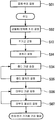
다음으로, 이와 같은 구성으로 된 본 실시 형태인 전자·전기 기기용 구리 합금의 제조 방법 및 전자·전기 기기용 구리 합금 소성 가공재의 제조 방법에 대해, 도 3 에 나타내는 플로우도를 참조하여 설명한다.Next, a method of manufacturing a copper alloy for electronic and electric devices and a method of producing a copper alloy calcined material for electronic / electric devices according to the present embodiment having the above-described structure will be described with reference to a flow chart shown in Fig.
본 실시 형태에서는, 도 3 에 나타내는 바와 같이, 용해·주조 공정 S01, 균질화/용체화 처리 공정 S02, 조가공 공정 S13, 열처리 공정 S14, 중간 가공 공정 S04, 중간 열처리 공정 S05, 마무리 가공 공정 S06, 마무리 열처리 공정 S07 을 구비하고 있고, 도 2 에 나타내는 제 1 실시형태에 있어서의 전자·전기 기기용 구리 합금의 제조 방법 중, 열간 가공 공정 S03 이 조가공 공정 S13 및 열처리 공정 S14 로 치환되어 있다. 따라서, 용해·주조 공정 S01, 균질화/용체화 처리 공정 S02, 중간 가공 공정 S04, 중간 열처리 공정 S05, 마무리 가공 공정 S06, 마무리 열처리 공정 S07 은, 제 1 실시형태와 동일하다.In this embodiment, as shown in Fig. 3, the dissolution / casting step S01, the homogenization / solution treatment step S02, the coarse machining step S13, the heat treatment step S14, the intermediate machining step S04, the intermediate heat treatment step S05, the finishing step S06, And a finishing heat treatment step S07. Of the copper alloy for electronic and electric equipment according to the first embodiment shown in Fig. 2, the hot working step S03 is replaced with the coarse machining step S13 and the heat treatment step S14. Therefore, the dissolution / casting step S01, the homogenization / solution treatment step S02, the intermediate machining step S04, the intermediate heat treatment step S05, the finishing step S06, and the final heat treatment step S07 are the same as those of the first embodiment.
(조가공 공정 S13)(Crude processing step S13)
조가공 공정 S13 에서는, 주조 조직의 균일화를 한층 더 촉진시키기 위해서, 균질화/용체화 공정 S02 를 거친 주괴에 대해 조가공을 실시한다. 또한, 이 조가공 공정 S13 에 있어서의 온도 조건은 특별히 한정은 없지만, 석출을 억제하기 위해서, 냉간 또는 온간 가공이 되는 -200 ℃ 내지 200 ℃ 의 범위 내로 하는 것이 바람직하다. 가공율에 대해서는, 20 % 이상이 바람직하고, 30 % 이상이 더욱 바람직하다. 또, 가공 방법에 대해서는, 특별히 한정은 없고, 예를 들어 압연, 선긋기, 압출, 홈 압연, 단조, 프레스 등을 채용할 수 있다.In the coarse machining step S13, the ingot having undergone the homogenizing / solubilizing step S02 is subjected to coarse machining to further promote the uniformization of the casting structure. The temperature condition in this coarse processing step S13 is not particularly limited, but it is preferable that the temperature is in the range of -200 캜 to 200 캜, which is cold or hot working, in order to suppress precipitation. The processing rate is preferably 20% or more, more preferably 30% or more. The processing method is not particularly limited, and for example, rolling, line drawing, extrusion, groove rolling, forging, pressing and the like can be employed.
(열처리 공정 S14)(Heat treatment step S14)
용체화의 철저를 위해, 조가공 공정 S13 후에 열처리를 실시한다. 열처리 조건은, 400 ℃ 이상 900 ℃ 이하에서, 비산화 분위기 중 또는 환원 분위기 중에서 실시하는 것이 바람직하다.In order to thoroughly solve the solution, a heat treatment is performed after the rough working step S13. The heat treatment is preferably carried out in a non-oxidizing atmosphere or a reducing atmosphere at a temperature of 400 ° C or more and 900 ° C or less.
또, 냉각 방법은, 물 퀀칭 등, 가열된 상기 구리 소재를, 60 ℃/min 이상의 냉각 속도로, 200 ℃ 이하로까지 냉각시키는 것이 바람직하다.It is preferable that the cooling method is such that the heated copper material such as water quenching is cooled to 200 占 폚 or less at a cooling rate of 60 占 폚 / min or more.
이와 같이 하여, 본 실시 형태인 전자·전기 기기용 구리 합금 및 전자·전기 기기용 구리 합금 소성 가공재가 제출되게 된다.In this way, copper alloys for electronic and electric appliances and copper alloy calcining materials for electric and electronic appliances according to the present embodiment are submitted.
또, 본 실시 형태인 전자·전기 기기용 부품 및 단자는, 상기 서술한 전자·전기 기기용 구리 합금 소성 가공재에 대해, 타발 가공, 굽힘 가공 등을 실시함으로써 제조된다.Parts and terminals for electronic and electric devices according to the present embodiment are manufactured by subjecting the above-described copper alloy calcination processing material for electronic / electric devices to punching, bending, and the like.
이상과 같은 구성으로 된 본 실시 형태인 전자·전기 기기용 구리 합금에 의하면, 제 1 실시형태와 동일한 작용 효과를 발휘하는 것이 가능해진다.According to the copper alloy for electric and electronic devices of the present embodiment having the above-described configuration, it is possible to exert the same operational effects as those of the first embodiment.
또, 본 실시 형태에 있어서는, 판 표면에 있어서의{220}면으로부터의 X 선 회절 강도의 비율 R{220}이 0.9 이하로 되어 있으므로, 압연 집합 조직인{220}면의 비율이 적고, 압연 방향에 대해 굽힘의 축이 평행이 되도록 굽힘 가공한 경우여도, 크랙의 발생을 억제할 수 있다. 따라서, 내력을 유지한 채로 굽힘 가공성을 향상시킬 수 있어 내력-굽힘 밸런스를 현저하게 향상시키는 것이 가능해진다.In the present embodiment, since the ratio R {220} of the X-ray diffraction intensity from the {220} plane on the surface of the plate is 0.9 or less, the ratio of the {220} plane as the rolled aggregate structure is small, It is possible to suppress the occurrence of cracks even when the bending is performed so that the axis of the bending is parallel to the direction of the bending. Therefore, the bending workability can be improved while maintaining the proof stress, and it is possible to remarkably improve the yield-bending balance.
(제 3 실시형태)(Third Embodiment)
다음으로, 본 발명의 제 3 실시형태인 전자·전기 기기용 구리 합금에 대해 설명한다.Next, a copper alloy for electronic / electric devices according to a third embodiment of the present invention will be described.
본 실시 형태인 전자·전기 기기용 구리 합금의 성분 조성은, Mg 를 1.3 mass% 이상 2.8 mass% 이하의 범위에서 함유하고, 잔부가 실질적으로 Cu 및 불가피 불순물로 되어 있어, 이른바 Cu-Mg 의 2 원계 합금으로 되어 있다.The composition of the copper alloy for electric and electronic devices according to the present embodiment contains Mg in a range of 1.3 mass% to 2.8 mass%, the remainder being substantially Cu and inevitable impurities, so-called Cu-Mg 2 It is made of a copper alloy.
또, 본 실시 형태인 전자·전기 기기용 구리 합금에 있어서는, 불순물 원소인 H, O, S, C 의 함유량이 이하와 같이 정해져 있다.In the copper alloy for electric and electronic devices according to the present embodiment, the contents of H, O, S, and C, which are impurity elements, are determined as follows.
H : 10 massppm 이하 H: 10 mass ppm or less
O : 100 massppm 이하 O: 100 mass ppm or less
S : 50 massppm 이하 S: 50 mass ppm or less
C : 10 massppm 이하C: 10 mass ppm or less
그리고, 본 실시 형태인 전자·전기 기기용 구리 합금에 있어서는, 압연 방향에 대해 평행 방향으로 인장 시험을 실시했을 때의 강도 TS 와 0.2 % 내력 YS 로부터 산출되는 항복비 YS/TS 가 90 % 를 초과하도록 구성되어 있다.In the copper alloy for electric and electronic devices according to the present embodiment, the strength TS when the tensile test is performed in the parallel direction with respect to the rolling direction and the yield ratio YS / TS calculated from the 0.2% proof stress YS exceed 90% .
또한, 본 실시 형태인 전자·전기 기기용 구리 합금에 있어서는, 평균 결정 입경이 50 ㎛ 이하로 되어 있다.In the case of the copper alloy for electric and electronic appliances according to the present embodiment, the average crystal grain size is 50 μm or less.
(항복비)(Yield ratio)
압연 방향에 대해 평행 방향으로 인장 시험을 실시했을 때의 강도 TS 와 0.2 % 내력 YS 로부터 산출되는 항복비 YS/TS 가 90 % 를 초과하고 있으면, 강도 TS 에 대해 상대적으로 0.2 % 내력이 높아진다. 굽힘성은, 파괴의 문제이며, 강도와 강한 상관이 있다. 이 때문에, 강도에 대해 상대적으로 0.2 % 내력이 높은 경우에는, 내력-굽힘 밸런스가 높아져, 굽힘 가공성이 우수한 것이 된다.If the strength TS and the yield ratio YS / TS calculated from the 0.2% proof stress YS when the tensile test is performed in the parallel direction with respect to the rolling direction are more than 90%, the 0.2% proof stress is increased relative to the strength TS. Bendability is a matter of failure and has a strong correlation with strength. Therefore, when the 0.2% proof stress is relatively high with respect to the strength, the proof stress-bending balance becomes high and the bending workability is excellent.
여기서, 상기 서술한 작용 효과를 확실하게 발휘시키기 위해서는, 항복비를 91 % 이상, 나아가서는 92 % 이상으로 하는 것이 바람직하다. 상기 서술한 전자·전기 기기용 구리 합금의 얻어지는 효과를 고려하면, 바람직한 상기 항복비의 상한치는 99.8 % 이지만, 이것으로 한정되는 일은 없다.Here, in order to reliably exhibit the above-described action and effect, the yield ratio is preferably 91% or more, and more preferably 92% or more. Considering the effect obtained by the above-described copper alloy for electric / electronic devices, the upper limit value of the yield ratio is preferably 99.8%, but the present invention is not limited thereto.
(평균 결정 입경)(Average crystal grain size)
본 실시 형태인 전자·전기 기기용 구리 합금에 있어서는, 평균 결정 입경이 50 ㎛ 이하로 되어 있다. 결정 입경이 작아지면 항복비 YS/TS 가 향상되는 점에서, 평균 결정 입경을 50 ㎛ 이하로 설정함으로써, 압연 방향에 대해 평행 방향에 있어서의 항복비 YS/TS 를 확실하게 90 % 초과로 하는 것이 가능해진다.In the copper alloy for electric and electronic devices according to the present embodiment, the average crystal grain size is 50 mu m or less. It is preferable that the yield ratio YS / TS in the parallel direction with respect to the rolling direction is surely made to exceed 90% by setting the average crystal grain size to 50 탆 or less in that the yield ratio YS / TS is improved when the crystal grain size becomes smaller It becomes possible.
또한, 평균 결정 입경은, 40 ㎛ 이하로 하는 것이 바람직하고, 30 ㎛ 이하로 하는 것이 더욱 바람직하다. 가장 바람직하게는 10 ㎛ 이하가 좋다. 상기 서술한 전자·전기 기기용 구리 합금의 얻어지는 효과를 고려하면, 바람직한 상기 평균 결정 입경의 하한치는 1 ㎛ 이지만, 이것으로 한정되는 일은 없다.The average crystal grain size is preferably 40 탆 or less, more preferably 30 탆 or less. And most preferably 10 mu m or less. Considering the effect obtained by the above-described copper alloy for electric / electronic devices, the lower limit of the average crystal grain size is preferably 1 占 퐉, but the present invention is not limited thereto.
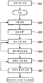
다음으로, 이와 같은 구성으로 된 본 실시 형태인 전자·전기 기기용 구리 합금의 제조 방법 및 전자·전기 기기용 구리 합금 소성 가공재의 제조 방법에 대해, 도 4 에 나타내는 플로우도를 참조하여 설명한다.Next, a method of manufacturing a copper alloy for electronic / electric devices and a method of producing a copper alloy sintered material for electronic / electric devices according to the present embodiment having the above-described structure will be described with reference to a flow chart shown in Fig.
본 실시 형태에서는, 도 4 에 나타내는 바와 같이, 용해·주조 공정 S01, 가열 공정 S22, 급냉 공정 S23, 중간 가공 공정 S04, 중간 열처리 공정 S05, 마무리 가공 공정 S06, 마무리 열처리 공정 S07 을 구비하고 있고, 도 2 에 나타내는 제 1 실시 형태에 있어서의 전자·전기 기기용 구리 합금의 제조 방법 중, 균질화/용체화 공정 S02 및 열간 가공 공정 S03 이 가열 공정 S22 및 급냉 공정 S23 으로 치환되어 있다. 따라서, 용해·주조 공정 S01, 중간 가공 공정 S04, 중간 열처리 공정 S05, 마무리 가공 공정 S06, 마무리 열처리 공정 S07 은 제 1 실시형태와 동일하다.In this embodiment, as shown in Fig. 4, a melting and casting step S01, a heating step S22, a quenching step S23, an intermediate machining step S04, an intermediate heat treatment step S05, a finishing step S06 and a finishing heat treatment step S07 are provided, 2, the homogenization / solution processing step S02 and the hot working step S03 are replaced by the heating step S22 and the quenching step S23. In the method of manufacturing the copper alloy for electronic / electrical equipments in the first embodiment shown in Fig. Therefore, the dissolution / casting step S01, the intermediate machining step S04, the intermediate heat treatment step S05, the finish machining step S06 and the finish heat treatment step S07 are the same as those of the first embodiment.
(가열 공정 S22)(Heating step S22)
가열 공정 S22 에서는, 얻어진 주괴의 균질화 및 용체화를 위해서 가열 처리를 실시한다. 주괴의 내부에는, 응고의 과정에 있어서 Mg 가 편석으로 농축됨으로써 발생한 Cu 와 Mg 를 주성분으로 하는 금속간 화합물 등이 존재하게 된다. 그래서, 이들의 편석 및 금속간 화합물 등을 소실 또는 저감시키기 위해서, 주괴를 400 ℃ 이상 900 ℃ 이하로까지 가열하는 가열 처리를 실시함으로써, 주괴 내에 있어서, Mg 를 균질로 확산시키거나, Mg 를 모상 중에 고용시키거나 하는 것이다. 또한, 이 가열 공정 S22 는, 비산화성 또는 환원성 분위기 중에서 실시하는 것이 바람직하다.In the heating step S22, heat treatment is performed for homogenization and solution conversion of the obtained ingot. Inside the ingot, an intermetallic compound mainly composed of Cu and Mg, which is formed by concentrating Mg into segregation in the solidification process, exists. Therefore, in order to eliminate or reduce segregation and intermetallic compounds of these, it is possible to homogeneously diffuse Mg in the ingot by performing heat treatment for heating the ingot to 400 ° C or more and 900 ° C or less, Or to hire them. The heating step S22 is preferably carried out in a non-oxidizing or reducing atmosphere.
여기서, 가열 온도가 400 ℃ 미만에서는, 용체화가 불완전해져, 모상 중에 Cu 와 Mg 를 주성분으로 하는 금속간 화합물이 많이 잔존할 우려가 있다. 한편, 가열 온도가 900 ℃ 를 초과하면, 구리 소재의 일부가 액상이 되어, 조직이나 표면 상태가 불균일해질 우려가 있다. 따라서, 가열 온도를 400 ℃ 이상 900 ℃ 이하의 범위로 설정하고 있다. 보다 바람직하게는 400 ℃ 이상 850 ℃ 이하, 더욱 바람직하게는 420 ℃ 이상 800 ℃ 이하로 한다.If the heating temperature is lower than 400 占 폚, solution conversion becomes incomplete and there is a possibility that a large amount of intermetallic compounds containing Cu and Mg as main components remain in the mother phase. On the other hand, if the heating temperature exceeds 900 占 폚, a part of the copper material becomes a liquid phase, and there is a fear that the texture and the surface state become uneven. Therefore, the heating temperature is set in the range of 400 DEG C or more and 900 DEG C or less. More preferably 400 ° C or more and 850 ° C or less, and further preferably 420 ° C or more and 800 ° C or less.
(급냉 공정 S23)(Quenching step S23)
급냉 공정 S23 에서는, 가열 공정 S22 에 있어서 400 ℃ 이상 900 ℃ 이하로까지 가열된 구리 소재를, 200 ℃ 이하의 온도로까지, 60 ℃/min 이상의 냉각 속도로 냉각시킨다.In the quenching step S23, the copper material heated to 400 DEG C or more and 900 DEG C or less in the heating step S22 is cooled to a temperature of 200 DEG C or less at a cooling rate of 60 DEG C / min or more.
이 급냉 공정 S23 에 의해, 모상 중에 고용된 Mg 가, Cu 와 Mg 를 주성분으로 하는 금속간 화합물로서 석출되는 것을 억제하고, 주사형 전자 현미경 관찰에 있어서, 입경 0.1 ㎛ 이상의 Cu 와 Mg 를 주성분으로 하는 금속간 화합물의 평균 개수를 1 개/㎛2 이하로 할 수 있다. 즉, 구리 소재를 Cu-Mg 과포화 고용체로 할 수 있는 것이다.In this quenching step S23, Mg dissolved in the mother phase is suppressed from being precipitated as an intermetallic compound mainly composed of Cu and Mg, and Cu and Mg as main components are observed in a scanning electron microscope The average number of intermetallic compounds can be set to 1 / mu m 2 or less. That is, the copper material can be a Cu-Mg supersaturated solid solution.
또한, 조가공의 효율화와 조직의 균일화를 위해서, 전술한 가열 공정 S22 후에 열간 가공을 실시하고, 이 열간 가공 후에 상기 서술한 급냉 공정 S23 을 실시하는 구성으로 해도 된다. 이 경우, 가공 방법으로 특별히 한정은 없고, 예를 들어 압연, 선긋기, 압출, 홈 압연, 단조, 프레스 등을 채용할 수 있다.Further, in order to improve the efficiency of coarse machining and uniformity of the structure, it is also possible to adopt a constitution in which hot working is performed after the above-described heating step S22 and the above-described quenching step S23 is performed after the hot working. In this case, the working method is not particularly limited, and for example, rolling, line drawing, extrusion, groove rolling, forging, pressing and the like can be adopted.
이와 같이 하여, 본 실시 형태인 전자·전기 기기용 구리 합금 및 전자·전기 기기용 구리 합금 소성 가공재가 제출되게 된다.In this way, copper alloys for electronic and electric appliances and copper alloy calcining materials for electric and electronic appliances according to the present embodiment are submitted.
또, 본 실시 형태인 전자·전기 기기용 부품 및 단자는, 상기 서술한 전자·전기 기기용 구리 합금 소성 가공재에 대해, 타발 가공, 굽힘 가공 등을 실시함으로써 제조된다.Parts and terminals for electronic and electric devices according to the present embodiment are manufactured by subjecting the above-described copper alloy calcination processing material for electronic / electric devices to punching, bending, and the like.
이상과 같은 구성으로 된 본 실시 형태인 전자·전기 기기용 구리 합금에 의하면, 제 1 실시형태와 동일한 작용 효과를 발휘하는 것이 가능해진다.According to the copper alloy for electric and electronic devices of the present embodiment having the above-described configuration, it is possible to exert the same operational effects as those of the first embodiment.
또, 본 실시 형태에 있어서는, 압연 방향에 대해 평행 방향으로 인장 시험을 실시했을 때의 강도 TS 와 0.2 % 내력 YS 로부터 산출되는 항복비 YS/TS 가 90 % 초과로 되어 있으므로, 내력-굽힘 밸런스가 높아져, 압연 방향에 대해 평행 방향에 있어서의 굽힘 가공성이 우수하다.In the present embodiment, since the yield strength YS / TS calculated from the strength TS and the 0.2% proof stress YS when the tensile test is performed in the parallel direction with respect to the rolling direction is more than 90%, the yield stress- So that the bending workability in the direction parallel to the rolling direction is excellent.
따라서, 릴레이나 대형 단자와 같이, 구리 합금 압연판의 압연 방향에 대해 평행 방향으로 굽힘 가공시킨 경우여도, 균열 등의 발생을 억제할 수 있다.Therefore, it is possible to suppress the occurrence of cracks or the like even when the copper alloy rolled plate is bent in the parallel direction with respect to the rolling direction, such as a relay or a large terminal.
또, 본 실시 형태의 전자·전기 기기용 구리 합금에 있어서는, 평균 결정 입경이 50 ㎛ 이하로 되어 있으므로, 항복비 YS/TS 를 향상시킬 수 있어, 압연 방향에 대해 평행 방향에 있어서의 항복비 YS/TS 를 확실하게 90 % 초과로 하는 것이 가능해진다.Since the average grain size of the copper alloy for electronic appliances of the present embodiment is 50 m or less, the yield ratio YS / TS can be improved, and the yield ratio YS in the parallel direction with respect to the rolling direction / TS can be surely made to exceed 90%.
이상, 본 발명의 실시형태인 전자·전기 기기용 구리 합금, 전자·전기 기기용 구리 합금 소성 가공재, 전자·전기 기기용 부품 및 단자에 대해 설명했지만, 본 발명은 이것으로 한정되는 일은 없고, 그 발명의 기술적 사상을 일탈하지 않는 범위에서 적절히 변경 가능하다.As described above, the copper alloy for electronic and electric appliances, the copper alloy firing processing material for electronic and electric appliances, and the parts and terminals for electronic and electric appliances, which are embodiments of the present invention, have been described, but the present invention is not limited thereto. And can be appropriately changed without departing from the technical idea of the invention.
예를 들어, 상기 서술한 실시형태에서는, 전자·전기 기기용 구리 합금의 제조 방법 및 전자·전기 기기용 구리 합금 소성 가공재의 제조 방법의 일례에 대해 설명했지만, 제조 방법은 본 실시 형태로 한정되는 일은 없고, 기존의 제조 방법을 적절히 선택하여 제조해도 된다.For example, in the above-described embodiments, a description has been given of an example of a method of manufacturing a copper alloy for electronic / electric equipment and a method of manufacturing a copper alloy calcining material for an electronic or electric appliance, but the manufacturing method is limited to this embodiment But may be manufactured by appropriately selecting an existing manufacturing method.
또, 본 실시 형태에서는, Cu-Mg 의 2 원계 합금을 예로 들어 설명했지만, 이것으로 한정되는 일은 없고, Sn, Zn, Al, Ni, Si, Mn, Li, Ti, Fe, Co, Cr, Zr, P 중 1 종 또는 2 종 이상을 합계로 0.01 mass% 이상 3.0 mass% 이하의 범위 내에서 함유하고 있어도 된다.However, the present invention is not limited to this. For example, Sn, Zn, Al, Ni, Si, Mn, Li, Ti, Fe, Co, Cr, Zr , And P in a total amount of 0.01 mass% or more and 3.0 mass% or less.
Sn, Zn, Al, Ni, Si, Mn, Li, Ti, Fe, Co, Cr, Zr, P 와 같은 원소는, Cu-Mg 합금의 강도 등의 특성을 향상시키는 원소인 점에서, 요구 특성에 따라 적절히 첨가하는 것이 바람직하다. 여기서, 첨가량의 합계를 0.01 mass% 이상으로 하고 있으므로, Cu-Mg 합금의 강도를 확실하게 향상시킬 수 있다. 한편, 첨가량의 합계를 3.0 mass% 이하로 하고 있으므로, 도전율을 확보할 수 있다.The elements such as Sn, Zn, Al, Ni, Si, Mn, Li, Ti, Fe, Co, Cr, Zr and P are elements that improve the strength and other properties of the Cu- It is preferable to add them appropriately. Here, since the total amount of addition is 0.01 mass% or more, the strength of the Cu-Mg alloy can be surely improved. On the other hand, the total amount of addition is 3.0 mass% or less, so that the conductivity can be ensured.
또한, 상기 서술한 원소를 함유하는 경우에는, 실시 형태에서 설명한 도전율의 규정은 적용되지 않지만, 석출물의 분포 상태로부터 Cu-Mg 의 과포화 고용체인 것을 확인할 수 있다.In the case of containing the above-described elements, the conductivity specification described in the embodiment is not applied, but it can be confirmed from the distribution state of the precipitates that the Cu-Mg is supersaturated.
실시예Example
(실시예 1)(Example 1)
이하에, 본 발명의 효과를 확인하기 위해 실시한 확인 실험의 결과에 대해 설명한다.Hereinafter, the results of verification tests conducted to confirm the effects of the present invention will be described.
H 함유량이 0.1 ppm 이하, O 함유량이 1.0 ppm 이하, S 함유량이 1.0 ppm 이하, C 함유량이 0.3 ppm 이하, Cu 의 순도 99.99 질량% 이상의 선별된 구리를 원료로서 준비하고, 이것을 고순도 알루미나 도가니 내에 장입(裝入)하여, 고순도 Ar 가스 (노점 -80 ℃ 이하) 분위기에 있어서 고주파 용해로를 사용하여 용해했다. 구리 합금 용탕 내에, 각종 원소를 첨가함과 함께, H, O 를 도입하는 경우에는, 용해 시의 분위기를 고순도 Ar 가스 (노점 -80 ℃ 이하), 고순도 N2 가스 (노점 -80 ℃ 이하), 고순도 O2 가스 (노점 -80 ℃ 이하), 고순도 H2 가스 (노점 -80 ℃ 이하) 를 사용하여, Ar-N2―H2 및 Ar-O2 혼합 가스 분위기로 했다. C 를 도입하는 경우에는, 용해에 있어서 용탕 표면에 C 입자를 피복시켜, 용탕과 접촉시켰다. 또, S 를 도입하는 경우에는, 직접, S 를 첨가했다. 이로써, 표 1 에 나타내는 성분 조성의 합금 용탕을 용제하고, 주형에 주탕(注湯)하여 주괴를 제출했다. 또한, 주괴의 크기는, 두께 약 120 mm × 폭 약 220 mm × 길이 약 300 mm 로 했다.A copper content of not more than 0.1 ppm, an O content of not more than 1.0 ppm, an S content of not more than 1.0 ppm, a C content of not more than 0.3 ppm and a Cu purity of not less than 99.99% by mass is prepared as a raw material and charged into a high purity alumina crucible And melted using a high-frequency melting furnace in a high-purity Ar gas (dew point -80 DEG C or lower) atmosphere. When the molten metal in the copper alloy, and also with the addition of various elements, introducing H, O, the atmosphere during melting high-purity Ar gas (dew point less than -80 ℃), high-purity N 2 gas (dew point less than -80 ℃), A mixed gas atmosphere of Ar-N 2 -H 2 and Ar-O 2 was used by using high purity O 2 gas (dew point -80 ° C or less) and high purity H 2 gas (dew point -80 ° C or less). In the case of introducing C, C particles were coated on the surface of the molten metal in the dissolution and brought into contact with the molten metal. When S is introduced, S is directly added. Thus, an alloy ingot having the composition shown in Table 1 was melted and the ingot was poured into the casting mold. In addition, the size of the ingot was about 120 mm in width x about 220 mm in width x about 300 mm in length.
계속해서 각 주괴에 대해, 절단·표면 연삭을 실시 후, 주괴의 성분 분석을 실시했다. 또한, Mg 및 그 밖의 첨가 원소의 분석은, 유도 결합 플라즈마 발광 분광 분석법으로 실시했다. 또, H 의 분석은, 열전도도법으로 실시하고, O, S, C 의 분석은, 적외선 흡수법으로 실시했다.Subsequently, each ingot was subjected to cutting and surface grinding, and then the composition of the ingot was analyzed. The analysis of Mg and other added elements was carried out by inductively coupled plasma emission spectroscopy. The analysis of H was carried out by the thermal conductivity method, and the analysis of O, S and C was carried out by the infrared absorption method.
얻어진 주괴로부터 주물 표면 근방을 면삭하여, 100 mm × 200 mm × 100 mm 의 블록을 잘랐다.The vicinity of the casting surface was machined from the obtained ingot, and a block of 100 mm x 200 mm x 100 mm was cut.
이 블록을, Ar 가스 분위기 중에 있어서, 표 2 에 기재된 온도 조건으로 4 시간의 가열을 실시하고, 균질화/용체화 처리를 실시했다.This block was subjected to a homogenization / solution treatment in an Ar gas atmosphere by heating under the temperature conditions shown in Table 2 for 4 hours.
열처리를 실시한 구리 소재를, 적절히, 최종 형상으로 적절한 형태로 하기 위해서, 절단함과 함께, 산화 피막을 제거하기 위해서 표면 연삭을 실시했다. 그 후, 상온에서, 표 2 에 기재된 압연율로 중간 압연을 실시했다.The copper material subjected to the heat treatment was appropriately cut in order to form a final shape appropriately, and surface grinding was performed in order to remove the oxide film. Thereafter, the intermediate rolling was carried out at room temperature under the rolling ratios shown in Table 2.
그리고, 얻어진 조재(條材)에 대해, 표 2 에 기재된 조건으로 솔트 배스로 중간 열처리를 실시했다. 그 후, 물 퀀칭을 실시했다.Then, the obtained joining material was subjected to an intermediate heat treatment with a salt bath under the conditions shown in Table 2. [ Thereafter, water quenching was performed.
다음으로, 표 2 에 나타내는 압연율로 마무리 압연을 실시하고, 두께 0.25 mm, 폭 약 200 mm 의 박판을 제출했다. 상기의 마무리 압연 시에는, 표면에 압연유를 도포하여 냉간 압연을 실시했다.Next, finishing rolling was carried out at the rolling rate shown in Table 2, and a thin plate having a thickness of 0.25 mm and a width of about 200 mm was submitted. At the time of the finish rolling, the surface was coated with rolling oil and subjected to cold rolling.
그리고, 마무리 압연 후에, 표 2 에 나타내는 조건으로, Ar 분위기 중에서 마무리 열처리를 실시하고, 그 후, 물 퀀칭을 실시하여, 특성 평가용 박판을 제조했다.After finishing rolling, finishing heat treatment was performed in an Ar atmosphere under the conditions shown in Table 2, and then water quenching was performed to produce a thin plate for evaluation of characteristics.
(가공성 평가)(Processability evaluation)
가공성의 평가로서, 전술한 중간 압연 및 마무리 압연 시에 있어서의 에지 균열의 유무를 관찰했다. 육안으로 에지 균열이 전혀 혹은 거의 확인되지 않은 것을 A, 길이 1 mm 미만의 작은 에지 균열이 발생한 것을 B, 길이 1 mm 이상 3 mm 미만의 에지 균열이 발생한 것을 C, 길이 3 mm 이상의 큰 에지 균열이 발생한 것을 D, 에지 균열에서 기인하여 압연 도중에 파단된 것을 E 로 했다.As evaluation of workability, the presence or absence of edge cracks during the above intermediate rolling and finish rolling was observed. B: edge crack of less than 1 mm in length, B: edge crack of less than 1 mm in length, C: large edge crack in length of 3 mm or more D that occurred, and E which was broken during the rolling due to edge cracks.
또한, 에지 균열의 길이란, 압연재의 폭방향 단부로부터 폭방향 중앙부를 향하는 에지 균열의 길이이다.The length of the edge crack is the length of the edge crack from the width direction end portion of the rolled material toward the widthwise center portion.
(석출물 관찰)(Observation of precipitates)
각 시료의 압연면에 대해, 경면 연마, 이온 에칭을 실시했다. Cu 와 Mg 를 주성분으로 하는 금속간 화합물의 석출 상태를 확인하기 위해, FE-SEM (전계 방출형 주사 전자 현미경) 을 사용하여, 1 만배의 시야 (약 120 ㎛2/시야) 에서 관찰을 실시했다.The rolling surface of each sample was subjected to mirror polishing and ion etching. In order to confirm the precipitation state of an intermetallic compound containing Cu and Mg as main components, observation was performed at a field of 10,000 magnifications (about 120 탆 2 / field of view) using FE-SEM (field emission scanning electron microscope) .
다음으로, Cu 와 Mg 를 주성분으로 하는 금속간 화합물의 밀도 (개/㎛2) 를 조사하기 위해서, 금속간 화합물의 석출 상태가 특이하지 않은 1 만배의 시야 (약 120 ㎛2/시야) 를 선택하고, 그 영역에서, 5 만배로 연속한 10 시야 (약 4.8 ㎛2/시야) 의 촬영을 실시했다. 금속간 화합물의 입경에 대해서는, 금속간 화합물의 장경 (도중에 입계에 접하지 않는 조건으로 입자 내에 가장 길게 그을 수 있는 직선의 길이) 과 단경 (장경과 직각으로 교차하는 방향에서, 도중에 입계에 접하지 않는 조건으로 가장 길게 그을 수 있는 직선의 길이) 의 평균치로 했다. 그리고, 입경 0.1 ㎛ 이상의 Cu 와 Mg 를 주성분으로 하는 금속간 화합물의 밀도 (개/㎛2) 를 구했다.Next, in order to examine the density (number / 탆 2 ) of the intermetallic compound containing Cu and Mg as the main component, a field of view of 10,000 times (about 120 탆 2 / field of view) (About 4.8 탆 2 / field of view) of 50,000 times consecutive in the area. With regard to the particle diameter of the intermetallic compound, it is preferable that the intermetallic compound has a long diameter (the length of a straight line that can be grasped the longest in the particle on the condition that the intermetallic compound does not touch the middle) and a short diameter The length of the straightest line that can be drawn in the longest condition). Then, the density (number / μm 2 ) of an intermetallic compound containing Cu and Mg as main components having a particle diameter of 0.1 μm or more was determined.
(기계적 특성)(Mechanical Properties)
특성 평가용 조재로부터 JIS Z 2241 에 규정되는 13B 호 시험편을 채취하고, JIS Z 2241 의 오프셋법에 의해, 0.2 % 내력 σ0.2 를 측정했다. 또, 탄성역의 기울기로부터 영률을 산출했다. 또한, 시험편은, 압연 방향에 수직인 방향에서 채취했다.The specimen No. 13B specified in JIS Z 2241 was taken from the specimen for characterization evaluation and 0.2% proof stress σ 0.2 was measured by the offset method of JIS Z 2241. The Young's modulus was calculated from the slope of the elasticity. Further, the test piece was taken in a direction perpendicular to the rolling direction.
(인장 시험의 파단 횟수)(Number of breaks of tensile test)
상기의 13B 호 시험편을 사용하여 인장 시험을 10 회 실시하고, 항복점에 접어들기 전에 탄성역에서 인장 시험편이 파단된 개수를 인장 시험의 파단 횟수로 하여, 측정을 실시했다. 또한 탄성역이란 응력 변형 곡선에 있어서 선형의 관계를 만족시키는 영역을 가리킨다. 이 파단 횟수가 많을수록, 개재물에 의해 가공성이 저하되고 있는 것이 된다.The tensile test was performed ten times using the above-mentioned No. 13B test piece, and the number of the tensile test pieces fractured in the elastic region before entering the yield point was measured as the number of breakage of the tensile test. The elastic zone refers to a region that satisfies the linear relationship in the stress-strain curve. The greater the number of breakages, the lower the workability due to inclusions.
(도전율)(Conductivity)
특성 평가용 조재로부터 폭 10 mm × 길이 150 mm 의 시험편을 채취하여, 4 단자법에 의해 전기 저항을 구했다. 또, 마이크로 미터를 사용하여 시험편의 치수 측정을 실시하여, 시험편의 체적을 산출했다. 그리고, 측정한 전기 저항값과 체적으로부터 도전율을 산출했다. 또한, 시험편은, 그 길이 방향이 특성 평가용 조재의 압연 방향에 대해 수직이 되도록 채취했다.A test piece having a width of 10 mm and a length of 150 mm was sampled from the specimen for evaluation of characteristics, and the electrical resistance was obtained by the four-terminal method. In addition, the dimensions of the test piece were measured using a micrometer, and the volume of the test piece was calculated. Then, the conductivity was calculated from the measured electrical resistance value and volume. Further, the test piece was sampled such that the longitudinal direction thereof was perpendicular to the rolling direction of the characteristics evaluation base material.
조건, 평가 결과에 대해, 표 1, 2, 3 에 나타낸다.Conditions, and evaluation results are shown in Tables 1, 2, and 3.


Mg 의 함유량이 본 발명의 범위보다 낮은 비교예 1 에 있어서는, 0.2 % 내력이 453 MPa 로 낮았다.In Comparative Example 1 in which the Mg content was lower than the range of the present invention, the 0.2% proof strength was as low as 453 MPa.
Mg 의 함유량이 본 발명의 범위보다 높은 비교예 2 에 있어서는, 중간 압연 시에 큰 에지 균열이 발생하여, 그 후의 특성 평가를 실시하는 것이 불가능했다.In Comparative Example 2 in which the content of Mg was higher than the range of the present invention, large edge cracks occurred at the time of intermediate rolling, and it was impossible to carry out the subsequent characteristic evaluation.
H 의 함유량이 본 발명의 범위보다 높은 비교예 3 에 있어서는, 중간 압연 시에 길이 1 mm 이상의 에지 균열이 발생했다. 또, 인장 시험을 10 회 실시했지만 모두 탄성역에서 인장 시험편이 파단되어 버려, 0.2 % 내력 σ0.2 를 측정할 수 없었다.In Comparative Example 3 in which the content of H was higher than the range of the present invention, edge cracks having a length of 1 mm or more were generated during intermediate rolling. In addition, although the tensile test was performed ten times, the tensile test specimen was broken in the elastic region, and the 0.2% proof stress σ 0.2 could not be measured.
O 의 함유량이 본 발명의 범위보다 높은 비교예 4 및 S 의 함유량이 본 발명의 범위보다 높은 비교예 5 에 있어서는, 중간 압연 시에 길이 1 mm 이상의 에지 균열이 발생했다. 또, 인장 시험을 10 회 실시한 결과, 탄성역에 있어서의 인장 시험편의 파단이 8 회 발생하고 있고, 개재물에 의한 가공성의 열화가 확인되었다.In Comparative Example 5 in which the content of O was higher than the range of the present invention and Comparative Example 4 in which the content of S was higher than the range of the present invention, edge cracks having a length of 1 mm or more occurred during intermediate rolling. As a result of ten tensile tests, ten tensile test specimens were broken in the elastic zone eight times, and deterioration of workability by inclusions was confirmed.
C 의 함유량이 본 발명의 범위보다 높은 비교예 6 에 있어서는, 인장 시험을 10 회 실시한 결과, 탄성역에 있어서의 인장 시험편의 파단이 6 회 발생하고 있고, 개재물에 의한 가공성의 열화가 확인되었다.In Comparative Example 6 in which the content of C was higher than the range of the present invention, tensile test was conducted 10 times, and as a result, tensile test pieces were broken 6 times in the elasticity region and deterioration of workability by inclusions was confirmed.
이에 대하여, Mg, H, O, S, C 의 함유량이 본 발명의 범위 내로 된 본 발명예 1-7 에 있어서는, 0.2 % 내력이 높고, 또한, 에지 균열의 발생도 없고, 인장 시험에 있어서의 탄성역에서의 파단도 확인되지 않았다.On the other hand, in the case of the present invention 1-7 in which the contents of Mg, H, O, S, and C were within the range of the present invention, the 0.2% proof stress was high and edge cracks did not occur, No fracture at the elastic station was confirmed.
또, Mg, H, O, S, C 의 함유량이 본 발명의 범위 내로 되고, 또한 첨가 원소를 함유하는 본 발명예 8-14 에 있어서도, 0.2 % 내력이 높고, 또한, 에지 균열의 발생도 없고, 인장 시험에 있어서의 탄성역에서의 파단도 확인되지 않았다.Also in the case of Inventive Examples 8-14 containing Mg, H, O, S, and C in the range of the present invention and containing the additive element, the 0.2% proof stress was high and no edge cracks , And no fracture at the elastic region in the tensile test was confirmed.
이상의 점에서, 본 발명예에 의하면, 기계적 특성이 우수함과 함께, 판두께를 얇고, 혹은, 선경을 가늘게 가공한 경우여도 결함의 발생을 억제하는 것이 가능한 전자·전기 기기용 구리 합금, 전자·전기 기기용 구리 합금 소성 가공재, 전자·전기 기기용 부품 및 단자를 제공할 수 있는 것이 확인되었다.In view of the above, according to the present invention, it is possible to provide a copper alloy for electronic and electric devices, which is superior in mechanical properties, can be made thinner in thickness, or can suppress the occurrence of defects even when the wire diameter is reduced, It was confirmed that it is possible to provide a copper alloy sintered material for a device, a component for an electric / electronic device, and a terminal.
(실시예 2)(Example 2)
다음으로, 실시예 1 과 동일한 방법에 의해, 표 4 에 나타내는 성분 조성의 주괴를 제출했다. 또한, 주괴의 크기는, 두께 약 150 mm × 폭 약 350 mm × 길이 약 2000 mm 로 했다. 얻어진 주괴로부터 주물 표면 근방을 10 mm 이상 면삭하고, 100 mm × 200 mm × 100 mm 의 블록을 잘랐다.Next, the ingot with the composition shown in Table 4 was submitted by the same method as in Example 1. The size of the ingot was about 150 mm in width x about 350 mm in width x about 2000 mm in length. A block of 100 mm x 200 mm x 100 mm was cut from the obtained ingot by machining the vicinity of the casting surface to 10 mm or more.
이 블록을, Ar 가스 분위기 중에 있어서, 표 5 에 기재된 온도 조건으로 4 시간의 가열을 실시하여, 균질화/용체화 처리를 실시했다.This block was subjected to homogenization / solution treatment by heating for 4 hours under the temperature conditions shown in Table 5 in an Ar gas atmosphere.
그 후, 표 5 에 기재된 조건으로 조가공으로서 조압연을 실시한 후, 솔트 배스를 사용하여 표 1 에 기재된 온도 조건으로 1 시간의 열처리를 실시하고, 물 퀀칭을 실시했다.Thereafter, rough rolling was carried out as rough working under the conditions shown in Table 5, followed by heat treatment for 1 hour at a temperature condition shown in Table 1 using a salt bath, and water quenching was carried out.
열처리를 실시한 구리 소재를 절단함과 함께, 산화 피막을 제거하기 위해서 표면 연삭을 실시했다. 그 후, 상온에서, 표 5 에 기재된 압연율로 중간 압연을 실시했다.The copper material subjected to the heat treatment was cut and surface grinding was performed in order to remove the oxide film. Thereafter, intermediate rolling was carried out at room temperature at the rolling rate shown in Table 5. [
그리고, 얻어진 조재에 대해, 표 5 에 기재된 조건으로 솔트 배스로 중간 열처리를 실시했다. 그 후, 물 퀀칭을 실시했다.Then, with respect to the obtained raw materials, the intermediate heat treatment was carried out with a salt bath under the conditions shown in Table 5. Thereafter, water quenching was performed.
다음으로, 표 5 에 나타내는 압연율로 마무리 압연을 실시하여, 두께 0.25 mm, 폭 약 200 mm 의 박판을 제출했다. 상기의 마무리 압연 시에는, 표면에 압연유를 도포하여 마무리 압연을 실시했다.Next, finishing rolling was carried out at the rolling rate shown in Table 5, and a thin plate having a thickness of 0.25 mm and a width of about 200 mm was submitted. At the time of the above-mentioned finish rolling, rolling oil was coated on the surface and finish rolling was performed.
그리고, 마무리 압연 후에, 표 5 에 나타내는 조건으로, Ar 분위기 중에서 마무리 열처리를 실시하고, 그 후, 물 퀀칭을 실시하여, 특성 평가용 박판을 제조했다.After finishing rolling, finishing heat treatment was performed in an Ar atmosphere under the conditions shown in Table 5, and then water quenching was performed to produce a thin plate for evaluation of characteristics.
실시예 1 과 마찬가지로, 가공성 평가 (중간 압연 및 마무리 압연 시에 있어서의 에지 균열의 유무), 석출물 관찰, 0.2 % 내력, 도전율의 측정을 실시했다. 또, 이하와 같은 순서에 의해, X 선 회절 강도, 굽힘 가공성을 평가했다.As in the case of Example 1, evaluation of workability (presence or absence of edge cracks during intermediate rolling and finishing rolling), observation of precipitates, 0.2% proof stress and conductivity were carried out. The X-ray diffraction intensity and the bending workability were evaluated by the following procedure.
(X 선 회절 강도)(X-ray diffraction intensity)
판 표면에 있어서의 {111}면으로부터의 X 선 회절 강도를 I{111},{200}면으로부터의 X 선 회절 강도 I{200},{220}면으로부터의 X 선 회절 강도 I{220},{311}면으로부터의 X 선 회절 강도 I{311}은, 다음과 같은 순서로 측정한다. 특성 평가용 박판으로부터 측정 시료를 채취하고, 반사법으로, 측정 시료에 대해 1 개의 회전축의 둘레의 X 선 회절 강도를 측정했다. 타겟에는 Cu 를 사용하고, Kα 의 X 선을 사용했다. 관 전류 40 mA, 관 전압 40 kV, 측정 각도 40 ∼ 150 °, 측정 스텝 0.02 °의 조건으로 측정하고, 회절각과 X 선 회절 강도의 프로파일에 있어서, X 선 회절 강도의 백그라운드를 제거 후, 각 회절면으로부터의 피크의 Kα1 과 Kα2 를 합한 적분 X 선 회절 강도 I 를 구하고, 이하의 식으로부터, R{220}의 값을 구했다.The X-ray diffraction intensity from the {111} plane on the plate surface is I {111}, the X-ray diffraction intensity I {200} from the {200} , The X-ray diffraction intensity I {311} from the {311} plane is measured in the following order. A measurement sample was taken from a thin plate for evaluation of characteristics, and X-ray diffraction intensity around one rotation axis was measured with respect to the measurement sample by a reflection method. Cu was used for the target, and X-ray of Kα was used. A tube current of 40 kV, a tube voltage of 40 kV, a measuring angle of 40 to 150 °, and a measuring step of 0.02 °, and after removing the background of the X-ray diffraction intensity in the profile of the diffraction angle and the X- The integrated X-ray diffraction intensity I obtained by adding K alpha 1 and K alpha 2 of the peak from the surface was determined and the value of R {220} was obtained from the following equation.
R{220}= I{220}/(I{111}+ I{200}+ I{220}+ I{311})R {220} = I {220} / (I {111} + I {200} + I {220} + I {311}
(굽힘 가공성)(Bending workability)
닛폰 신동 협회 기술 표준 JCBA-T307 : 2007 의 4 시험 방법에 준거하여 굽힘 가공을 실시했다.Bending was performed in accordance with the 4th test method of JCBA-T307: 2007, the technical standard of the Nippon Shindong Association.
압연 방향과 시험편의 길이 방향이 수직이 되도록, 특성 평가용 조재로부터 폭 10 mm × 길이 30 mm 의 시험편을 복수 채취하고, 굽힘 각도가 90 도, 굽힘 반경 0.25 mm 의 W 형의 지그를 사용하여 W 굽힘 시험을 실시했다.A plurality of test specimens having a width of 10 mm and a length of 30 mm were taken from the specimens for evaluation of characteristics so that the rolling direction and the longitudinal direction of the test specimens were perpendicular to each other. A W type jig having a bending angle of 90 degrees and a bending radius of 0.25 mm was used to measure W A bending test was carried out.
그리고, 굽힘부의 외주부를 육안으로 확인하여 균열이 관찰된 경우에는 B, 파단이나 미세한 균열을 확인할 수 없는 경우를 A 로 하여 판정을 실시했다.The outer circumferential portion of the bent portion was visually inspected, and B was determined when cracks were observed, and A when fracture or fine cracks were not observed.
성분 조성, 제조 조건, 평가 결과에 대해, 표 4, 5, 6 에 나타낸다.The composition, production conditions, and evaluation results are shown in Tables 4, 5, and 6.


{220}면으로부터의 X 선 회절 강도의 비율 R{220}이, 0.9 이하로 된 본 발명예 101-114 에 있어서는, 0.2 % 내력이 높고, 또한, 굽힘 가공성도 양호하고, 내력-굽힘 밸런스가 우수한 것이 확인되었다.In the case of the examples 101-114 in which the ratio R {220} of the X-ray diffraction intensity from the {220} plane was 0.9 or less, the 0.2% proof stress was high and the bending workability was good and the proof- Excellent.
(실시예 3)(Example 3)
다음으로, 실시예 1 과 동일한 방법에 의해, 표 7 에 나타내는 성분 조성의 주괴를 제출했다. 또한, 주괴의 크기는, 두께 약 150 mm × 폭 약 350 mm × 길이 약 2000 mm 로 했다. 얻어진 주괴로부터 주물 표면 근방을 10 mm 이상 면삭하고, 100 mm × 200 mm × 100 mm 의 블록을 잘랐다.Next, the ingot having the composition shown in Table 7 was submitted by the same method as in Example 1. The size of the ingot was about 150 mm in width x about 350 mm in width x about 2000 mm in length. A block of 100 mm x 200 mm x 100 mm was cut from the obtained ingot by machining the vicinity of the casting surface to 10 mm or more.
이 블록을, Ar 가스 분위기 중에 있어서, 표 8 에 기재된 온도 조건으로 4 시간의 가열을 실시하는 가열 공정을 실시하고, 그 후, 물 퀀칭을 실시했다.This block was subjected to a heating step of heating for 4 hours under the temperature conditions shown in Table 8 in an Ar gas atmosphere, and then water quenching was performed.
열처리 후의 주괴를 절단함과 함께, 산화 피막을 제거하기 위해서 표면 연삭을 실시했다.The ingot after the heat treatment was cut and surface grinding was performed to remove the oxide film.
그 후, 상온에서, 표 1 에 기재된 압연율로 중간 압연을 실시했다. 그리고, 얻어진 조재에 대해, 표 8 에 기재된 온도의 조건으로 솔트 배스로 중간 열처리를 실시했다. 그 후, 물 퀀칭을 실시했다.Thereafter, intermediate rolling was carried out at room temperature at the rolling rate shown in Table 1. Then, with respect to the obtained raw materials, the intermediate heat treatment was carried out with a salt bath under the conditions of the temperature shown in Table 8. Thereafter, water quenching was performed.
다음으로, 표 8 에 나타내는 압연율로 마무리 압연을 실시하고, 두께 0.25 mm, 폭 약 200 mm 의 조재를 제출했다.Next, finish rolling was carried out at the rolling rate shown in Table 8, and the raw material having a thickness of 0.25 mm and a width of about 200 mm was submitted.
그리고, 마무리 압연 후에, 표 8 에 나타내는 조건으로, Ar 분위기 중에서 마무리 열처리를 실시하고, 그 후, 물 퀀칭을 실시하여, 특성 평가용 조재를 제조했다.After finishing rolling, finishing heat treatment was performed in an Ar atmosphere under the conditions shown in Table 8, and then water quenching was performed to produce a specimen for characterization evaluation.
실시예 1 과 마찬가지로, 가공성 평가 (중간 압연 및 마무리 압연 시에 있어서의 에지 균열의 유무), 석출물 관찰, 도전율의 측정을 실시했다. 또, 이하와 같은 순서에 의해, 평균 결정 입경, 기계적 특성을 평가했다.As in Example 1, evaluation of workability (presence or absence of edge cracks during intermediate rolling and finish rolling), observation of precipitates, and measurement of conductivity were carried out. The average crystal grain size and mechanical characteristics were evaluated by the following procedure.
(평균 결정 입경)(Average crystal grain size)
각 시료에 있어서, 압연면을 경면 연마한 후 에칭을 실시하고, 광학 현미경으로, 압연 방향이 사진의 가로가 되도록 촬영하고, 1000 배의 시야 (약 300 × 200 ㎛2) 에서 관찰을 실시했다. 그리고, 결정 입경을 JIS H 0501 의 절단법에 따라, 사진의 세로, 가로의 소정 길이의 선분을 5 개씩 긋고, 완전히 잘리는 결정립수를 세어, 그 절단 길이의 평균치를 평균 결정 입경으로서 산출했다.In each sample, the rolled surface was mirror-polished and then etched. Using an optical microscope, the rolled surface was photographed such that the rolling direction was the width of the photograph, and observation was performed at a magnification of 1000 times (approximately 300 x 200 탆 2 ). Then, the number of crystal grains to be completely cut was counted by drawing five pieces of line segments each having a predetermined length in the longitudinal and lateral directions of the photograph according to the cutting method of JIS H 0501, and the average value of the cut lengths was calculated as the average crystal grain size.
결정 입경이 10 ㎛ 이하로 미세한 경우에는, SEM-EBSD (Electron Backscatter Diffraction Patterns) 측정 장치에 의해, 평균 결정 입경을 측정했다. 내수 연마지, 다이아몬드 지립을 사용하여 기계 연마를 실시한 후, 콜로이달 실리카 용액을 사용하여 마무리 연마를 실시했다. 그 후, 주사형 전자 현미경을 사용하여, 시료 표면의 측정 범위 내의 개개의 측정점 (픽셀) 에 전자선을 조사하고, 후방 산란 전자선 회절에 의한 방위 해석에 의해, 인접하는 측정점간의 방위차가 15 °이상이 되는 측정점간을 대경각 입계로 하고, 15 °이하를 소경각 입계로 했다. 대경각 입계를 사용하여, 결정립계 맵을 작성하고, JIS H 0501 의 절단법에 준거하여, 결정립계 맵에 대해, 세로, 가로의 소정 길이의 선분을 5 개씩 긋고, 완전히 잘리는 결정립수를 세어, 그 절단 길이의 평균치를 평균 결정 입경으로 했다.When the crystal grain size is as small as 10 mu m or less, the average crystal grain size was measured by an SEM-EBSD (Electron Backscatter Diffraction Patterns) measuring apparatus. Mechanical polishing was carried out using a water-borne abrasive paper or a diamond abrasive, and then a finish polishing was carried out using a colloidal silica solution. Thereafter, electron beams are irradiated to individual measurement points (pixels) within the measurement range of the surface of the sample using a scanning electron microscope, and the azimuthal difference between the adjacent measurement points is 15 degrees or more The measurement points were set at the large-diameter side and the small-diameter side at 15 ° or less. A grain boundary map is created using the large grain boundary grain boundaries, and five segments of a predetermined length in the longitudinal and lateral directions are drawn on the grain boundary map in accordance with the cutting method of JIS H 0501 to count the number of completely- The average value of the length was defined as an average crystal grain size.
(기계적 특성)(Mechanical Properties)
특성 평가용 조재로부터 JIS Z 2241 에 규정되는 13B 호 시험편을 채취하고, JIS Z 2241 의 오프셋법에 의해, 강도 TS, 0.2 % 내력 YS 를 측정했다. 또한, 시험편은, 압연 방향에 평행한 방향에서 채취했다. 그리고, 얻어진 강도 TS, 0.2 % 내력 YS 로부터, 항복비 YS/TS 를 산출했다.The specimen No. 13B specified in JIS Z 2241 was taken from the specimens for characterization evaluation and the strength TS and the 0.2% proof stress YS were measured by the offset method of JIS Z 2241. Further, the test piece was taken in a direction parallel to the rolling direction. Then, the yield ratio YS / TS was calculated from the obtained strength TS and 0.2% proof stress YS.
성분 조성, 제조 조건, 평가 결과에 대해, 표 7, 8, 9 에 나타낸다.The composition, production conditions, and evaluation results are shown in Tables 7, 8, and 9.


본 발명예 201-214 에 있어서는, 모두 항복비 YS/TS 가 90 % 를 초과하고 있고, 강도 TS, 0.2 % 내력 YS 모두 높아져 있었다. 또한, 굽힘 가공성도 양호한 것이 확인되었다.In the present invention, the yield ratio YS / TS exceeded 90%, and both the strength TS and the 0.2% proof stress YS were increased. Further, it was confirmed that the bending workability was also good.
산업상 이용가능성Industrial availability
본 발명의 전자·전기 기기용 구리 합금을 사용함으로써, 제조 수율을 향상할 수 있다.By using the copper alloy for electric / electronic devices of the present invention, the production yield can be improved.
Claims (14)
H 의 함유량이 10 massppm 이하, O 의 함유량이 100 massppm 이하, S 의 함유량이 50 massppm 이하, C 의 함유량이 10 massppm 이하로 되어 있는 것을 특징으로 하는 전자·전기 기기용 구리 합금.Mg in a range from 1.3 mass% to 2.8 mass%, the remainder being substantially Cu and inevitable impurities,
Wherein the H content is 10 mass ppm or less, the O content is 100 mass ppm or less, the S content is 50 mass ppm or less, and the C content is 10 mass ppm or less.
주사형 전자 현미경 관찰에 있어서, 입경 0.1 ㎛ 이상의 Cu 와 Mg 를 주성분으로 하는 금속간 화합물의 평균 개수가, 1 개/㎛2 이하로 되어 있는 것을 특징으로 하는 전자·전기 기기용 구리 합금.The method according to claim 1,
Wherein the average number of intermetallic compounds mainly composed of Cu and Mg having a particle size of 0.1 占 퐉 or more is 1 / 占 퐉 2 or less in a scanning electron microscope observation.
도전율 σ (% IACS) 가, Mg 의 함유량을 A 원자% 로 했을 때에,
σ ≤ 1.7241/(-0.0347 × A2 + 0.6569 × A + 1.7) × 100 의 범위 내로 되어 있는 것을 특징으로 하는 전자·전기 기기용 구리 합금.3. The method according to claim 1 or 2,
When the conductivity? (% IACS) is defined as the atomic% of Mg,
σ ≤ 1.7241 / (- 0.0347 × A 2 + 0.6569 × A + 1.7) × 100 The copper alloy for electric or electronic device, characterized in that it is in the range of.
Sn, Zn, Al, Ni, Si, Mn, Li, Ti, Fe, Co, Cr, Zr, P 중 1 종 또는 2 종 이상을 합계로 0.01 mass% 이상 3.0 mass% 이하의 범위 내에서 함유하고 있는 것을 특징으로 하는 전자·전기 기기용 구리 합금.3. The method according to claim 1 or 2,
At least one of Sn, Zn, Al, Ni, Si, Mn, Li, Ti, Fe, Co, Cr, Zr and P in a total amount of not less than 0.01 mass% and not more than 3.0 mass% Wherein the copper alloy is used for an electronic or electric appliance.
0.2 % 내력이 400 MPa 이상의 기계적 특성을 갖는 것을 특징으로 하는 전자·전기 기기용 구리 합금.5. The method according to any one of claims 1 to 4,
And a 0.2% proof stress has a mechanical characteristic of 400 MPa or more.
판 표면에 있어서의 {111}면으로부터의 X 선 회절 강도를 I{111},{200}면으로부터의 X 선 회절 강도를 I{200},{220}면으로부터의 X 선 회절 강도를 I{220},{311}면으로부터의 X 선 회절 강도를 I{311},{220}면으로부터의 X 선 회절 강도의 비율 R{220}을 R{220}= I{220}/(I{111}+ I{200}+ I{220}+ I{311}) 로 한 경우에, R{220}이 0.9 이하로 되어 있는 것을 특징으로 하는 전자·전기 기기용 구리 합금.6. The method according to any one of claims 1 to 5,
The X-ray diffraction intensity from the {111} plane on the plate surface is represented by I {111}, the X-ray diffraction intensity from the {200} plane is I {200} 220}, the X-ray diffraction intensity from the {311} plane is I {311}, the ratio R {220} of the X-ray diffraction intensity from the {220} } + I {200} + I {220} + I {311}, R {220} is 0.9 or less.
R{220}이 0.3 이상 0.9 이하로 되어 있는 것을 특징으로 하는 전자·전기 기기용 구리 합금.The method according to claim 6,
Wherein R {220} is 0.3 or more and 0.9 or less.
압연 방향에 대해 평행 방향으로 인장 시험을 실시했을 때의 강도 TS 와, 0.2 % 내력 YS 로부터 산출되는 항복비 YS/TS 가 90 % 를 초과하는 것을 특징으로 하는 전자·전기 기기용 구리 합금.8. The method according to any one of claims 1 to 7,
Wherein the strength TS when the tensile test is performed in the parallel direction with respect to the rolling direction and the yield ratio YS / TS calculated from the 0.2% proof stress YS exceed 90%.
평균 결정 입경이 50 ㎛ 이하로 되어 있는 것을 특징으로 하는 전자·전기 기기용 구리 합금.9. The method of claim 8,
Wherein the average grain size of the copper alloy is 50 占 퐉 or less.
상기 구리 소재를 400 ℃ 이상 900 ℃ 이하의 온도로까지 가열함과 함께, 가열된 상기 구리 소재를 60 ℃/min 이상의 냉각 속도로 200 ℃ 이하로까지 냉각시키는 열처리 공정과, 상기 구리 소재를 소성 가공하는 소성 가공 공정을 갖는 제조 방법에 의해 성형된 것을 특징으로 하는 전자·전기 기기용 구리 합금 소성 가공재.11. The method of claim 10,
A heat treatment step of heating the copper material to a temperature of 400 ° C or more and 900 ° C or less and cooling the heated copper material to a temperature of 200 ° C or less at a cooling rate of 60 ° C / min or more, Wherein the copper alloy is formed by a manufacturing method having a plastic working process.
표면에 Sn 도금이 실시되어 있는 것을 특징으로 하는 전자·전기 기기용 구리 합금 소성 가공재.The method according to claim 10 or 11,
Wherein the surface of the copper alloy is plated with Sn.
Applications Claiming Priority (5)
| Application Number | Priority Date | Filing Date | Title |
|---|---|---|---|
| JPJP-P-2013-159642 | 2013-07-31 | ||
| JP2013159642 | 2013-07-31 | ||
| JP2014117998A JP5962707B2 (en) | 2013-07-31 | 2014-06-06 | Copper alloy for electronic / electric equipment, copper alloy plastic working material for electronic / electric equipment, manufacturing method of copper alloy plastic working material for electronic / electric equipment, electronic / electric equipment parts and terminals |
| JPJP-P-2014-117998 | 2014-06-06 | ||
| PCT/JP2014/069942 WO2015016218A1 (en) | 2013-07-31 | 2014-07-29 | Copper alloy for electronic and electrical equipment, plastically worked copper alloy material for electronic and electrical equipment, and component and terminal for electronic and electrical equipment |
Publications (1)
| Publication Number | Publication Date |
|---|---|
| KR20160036038A true KR20160036038A (en) | 2016-04-01 |
Family
ID=52431750
Family Applications (1)
| Application Number | Title | Priority Date | Filing Date |
|---|---|---|---|
| KR1020167001487A KR20160036038A (en) | 2013-07-31 | 2014-07-29 | Copper alloy for electronic and electrical equipment, plastically worked copper alloy material for electronic and electrical equipment, and component and terminal for electronic and electrical equipment |
Country Status (9)
| Country | Link |
|---|---|
| US (1) | US10294547B2 (en) |
| EP (1) | EP3029168A4 (en) |
| JP (1) | JP5962707B2 (en) |
| KR (1) | KR20160036038A (en) |
| CN (1) | CN105392908A (en) |
| MX (1) | MX2016001257A (en) |
| MY (1) | MY178741A (en) |
| TW (1) | TWI521072B (en) |
| WO (1) | WO2015016218A1 (en) |
Cited By (1)
| Publication number | Priority date | Publication date | Assignee | Title |
|---|---|---|---|---|
| KR20180130803A (en) * | 2017-05-30 | 2018-12-10 | 현대자동차주식회사 | Alloy for garnish of vehicle and garnish for vehicle |
Families Citing this family (22)
| Publication number | Priority date | Publication date | Assignee | Title |
|---|---|---|---|---|
| DE19900673A1 (en) * | 1999-01-11 | 2000-07-13 | Basf Ag | Use of binding partners for 5-HT5 receptors for the treatment of neurodegenerative and neuropsychiatric disorders |
| EP2570506B1 (en) * | 2010-05-14 | 2016-04-13 | Mitsubishi Materials Corporation | Copper alloy for electronic device, method for producing this alloy, and copper alloy rolled material for this device |
| JP5903838B2 (en) | 2011-11-07 | 2016-04-13 | 三菱マテリアル株式会社 | Copper alloy for electronic equipment, copper material for electronic equipment, copper alloy manufacturing method for electronic equipment, copper alloy plastic working material for electronic equipment, and electronic equipment parts |
| JP5903842B2 (en) | 2011-11-14 | 2016-04-13 | 三菱マテリアル株式会社 | Copper alloy, copper alloy plastic working material, and method for producing copper alloy plastic working material |
| CN107208189B (en) | 2015-09-09 | 2020-08-04 | 三菱综合材料株式会社 | Copper alloy, copper alloy plastic working material, assembly, terminal, and bus bar |
| JP6155407B1 (en) * | 2015-09-09 | 2017-06-28 | 三菱マテリアル株式会社 | Copper alloys for electronic and electrical equipment, electronic and electrical equipment parts, terminals, and bus bars |
| JP6156600B1 (en) * | 2015-09-09 | 2017-07-05 | 三菱マテリアル株式会社 | Copper alloy for electronic and electric equipment, copper alloy plastic working material for electronic and electric equipment, parts for electronic and electric equipment, terminals, and bus bars |
| TWI701351B (en) | 2015-09-09 | 2020-08-11 | 日商三菱綜合材料股份有限公司 | Copper alloy for electronic and electric device, plastically-worked copper alloy material for electronic and electric device, electronic and electric device, terminal and bus bar |
| EP3348656B1 (en) * | 2015-09-09 | 2020-12-30 | Mitsubishi Materials Corporation | Copper alloy for electronic/electrical device, copper alloy plastically worked material for electronic/electrical device, component for electronic/electrical device, terminal, and busbar |
| WO2017090638A1 (en) * | 2015-11-27 | 2017-06-01 | 三菱マテリアル株式会社 | Tin-plated copper terminal material, terminal, and wire terminal part structure |
| JP6226097B2 (en) * | 2016-03-30 | 2017-11-08 | 三菱マテリアル株式会社 | Copper alloy for electronic and electrical equipment, copper alloy sheet material for electronic and electrical equipment, electronic and electrical equipment parts, terminals, bus bars, and movable pieces for relays |
| WO2017170733A1 (en) | 2016-03-30 | 2017-10-05 | 三菱マテリアル株式会社 | Copper alloy for electronic and electrical equipment, copper alloy plate strip for electronic and electrical equipment, component for electronic and electrical equipment, terminal, busbar, and movable piece for relays |
| JP6226098B2 (en) * | 2016-03-30 | 2017-11-08 | 三菱マテリアル株式会社 | Copper alloy for electronic and electrical equipment, copper alloy sheet material for electronic and electrical equipment, electronic and electrical equipment parts, terminals, bus bars, and movable pieces for relays |
| US11203806B2 (en) | 2016-03-30 | 2021-12-21 | Mitsubishi Materials Corporation | Copper alloy for electronic and electrical equipment, copper alloy plate strip for electronic and electrical equipment, component for electronic and electrical equipment, terminal, busbar, and movable piece for relay |
| JP6299802B2 (en) | 2016-04-06 | 2018-03-28 | 三菱マテリアル株式会社 | Superconducting stabilizer, superconducting wire and superconducting coil |
| JP2018077942A (en) * | 2016-11-07 | 2018-05-17 | 住友電気工業株式会社 | Coated electric wire, electric wire having terminal, copper alloy wire and copper alloy twisted wire |
| JP6828444B2 (en) * | 2017-01-10 | 2021-02-10 | 日立金属株式会社 | Conductive wire manufacturing method and cable manufacturing method |
| KR101875807B1 (en) * | 2018-03-14 | 2018-07-06 | 주식회사 풍산 | Method for manufacturing a copper alloy material for automobiles and electric/electronic parts excellent in high strength and bending workability |
| KR20200134215A (en) | 2018-03-30 | 2020-12-01 | 미쓰비시 마테리알 가부시키가이샤 | Copper alloy for electronic and electric equipment, copper alloy plate strip for electronic and electric equipment, parts for electronic and electric equipment, terminals, and busbars |
| JP6780187B2 (en) | 2018-03-30 | 2020-11-04 | 三菱マテリアル株式会社 | Copper alloys for electronic / electrical equipment, copper alloy strips for electronic / electrical equipment, parts for electronic / electrical equipment, terminals, and busbars |
| JP7116870B2 (en) * | 2019-03-29 | 2022-08-12 | 三菱マテリアル株式会社 | Copper alloy sheet, copper alloy sheet with plating film, and method for producing the same |
| JP7024925B2 (en) * | 2019-11-29 | 2022-02-24 | 三菱マテリアル株式会社 | Copper alloys, plastic working materials for copper alloys, parts for electronic and electrical equipment, terminals, bus bars, heat dissipation boards |
Family Cites Families (26)
| Publication number | Priority date | Publication date | Assignee | Title |
|---|---|---|---|---|
| JPS5344136B2 (en) * | 1974-12-23 | 1978-11-27 | ||
| JPS58128292A (en) * | 1982-01-26 | 1983-07-30 | Furukawa Electric Co Ltd:The | Thin strip of phosphorus copper brazing filler metal |
| JPH04350137A (en) * | 1991-07-19 | 1992-12-04 | Mitsubishi Shindoh Co Ltd | Connector material made of cu alloy having high strength |
| JPH0718354A (en) | 1993-06-30 | 1995-01-20 | Mitsubishi Electric Corp | Copper alloy for electronic appliance and its production |
| JP3904118B2 (en) * | 1997-02-05 | 2007-04-11 | 株式会社神戸製鋼所 | Copper alloy for electric and electronic parts and manufacturing method thereof |
| JPH11199954A (en) * | 1998-01-20 | 1999-07-27 | Kobe Steel Ltd | Copper alloy for electrical and electronic part |
| JP3797786B2 (en) * | 1998-03-06 | 2006-07-19 | 株式会社神戸製鋼所 | Copper alloy for electrical and electronic parts |
| JP2002038227A (en) * | 2000-05-16 | 2002-02-06 | Nippon Mining & Metals Co Ltd | Phosphor bronze bar excellent in deep drawing and its production method |
| JP4610765B2 (en) * | 2001-03-21 | 2011-01-12 | 株式会社神戸製鋼所 | Hot-rollable phosphor bronze |
| US7789977B2 (en) * | 2006-10-26 | 2010-09-07 | Hitachi Cable, Ltd. | Rolled copper foil and manufacturing method thereof |
| JP4466688B2 (en) | 2007-07-11 | 2010-05-26 | 日立電線株式会社 | Rolled copper foil |
| JP4974197B2 (en) | 2009-08-28 | 2012-07-11 | 古河電気工業株式会社 | Copper material for sputtering target and method for producing the same |
| JP4516154B1 (en) | 2009-12-23 | 2010-08-04 | 三菱伸銅株式会社 | Cu-Mg-P copper alloy strip and method for producing the same |
| JP5088384B2 (en) * | 2010-01-26 | 2012-12-05 | 三菱マテリアル株式会社 | High strength and high conductivity copper alloy |
| JP5045784B2 (en) * | 2010-05-14 | 2012-10-10 | 三菱マテリアル株式会社 | Copper alloy for electronic equipment, method for producing copper alloy for electronic equipment, and rolled copper alloy material for electronic equipment |
| EP2570506B1 (en) * | 2010-05-14 | 2016-04-13 | Mitsubishi Materials Corporation | Copper alloy for electronic device, method for producing this alloy, and copper alloy rolled material for this device |
| JP5045783B2 (en) | 2010-05-14 | 2012-10-10 | 三菱マテリアル株式会社 | Copper alloy for electronic equipment, method for producing copper alloy for electronic equipment, and rolled copper alloy material for electronic equipment |
| JP5088425B2 (en) * | 2011-01-13 | 2012-12-05 | 三菱マテリアル株式会社 | Copper alloy, copper alloy sheet and conductive member for electronic and electrical equipment |
| JP5703975B2 (en) | 2011-06-06 | 2015-04-22 | 三菱マテリアル株式会社 | Copper alloy for electronic equipment, method for producing copper alloy for electronic equipment, and rolled copper alloy material for electronic equipment |
| US20140096877A1 (en) | 2011-06-06 | 2014-04-10 | Mitsubishi Materials Corporation | Copper alloy for electronic devices, method for producing copper alloy for electronic devices, copper alloy plastic working material for electronic devices, and component for electronic devices |
| JP5903839B2 (en) * | 2011-11-07 | 2016-04-13 | 三菱マテリアル株式会社 | Copper alloy for electronic equipment, method for producing copper alloy for electronic equipment, copper alloy plastic working material for electronic equipment and electronic equipment parts |
| JP5903832B2 (en) * | 2011-10-28 | 2016-04-13 | 三菱マテリアル株式会社 | Copper alloy for electronic equipment, method for producing copper alloy for electronic equipment, rolled copper alloy material for electronic equipment, and electronic equipment parts |
| JP5903838B2 (en) * | 2011-11-07 | 2016-04-13 | 三菱マテリアル株式会社 | Copper alloy for electronic equipment, copper material for electronic equipment, copper alloy manufacturing method for electronic equipment, copper alloy plastic working material for electronic equipment, and electronic equipment parts |
| JP5910004B2 (en) | 2011-11-07 | 2016-04-27 | 三菱マテリアル株式会社 | Copper alloy for electronic equipment, method for producing copper alloy for electronic equipment, copper alloy plastic working material for electronic equipment and electronic equipment parts |
| JP2013104096A (en) | 2011-11-14 | 2013-05-30 | Mitsubishi Materials Corp | Copper alloy for electronic equipment, method for producing copper alloy for electronic equipment, copper alloy plastic working material for electronic equipment, and part for electronic equipment |
| JP5903842B2 (en) * | 2011-11-14 | 2016-04-13 | 三菱マテリアル株式会社 | Copper alloy, copper alloy plastic working material, and method for producing copper alloy plastic working material |
-
2014
- 2014-06-06 JP JP2014117998A patent/JP5962707B2/en active Active
- 2014-07-28 TW TW103125685A patent/TWI521072B/en active
- 2014-07-29 MY MYPI2016700236A patent/MY178741A/en unknown
- 2014-07-29 CN CN201480039932.5A patent/CN105392908A/en active Pending
- 2014-07-29 EP EP14831793.6A patent/EP3029168A4/en not_active Withdrawn
- 2014-07-29 MX MX2016001257A patent/MX2016001257A/en unknown
- 2014-07-29 WO PCT/JP2014/069942 patent/WO2015016218A1/en active Application Filing
- 2014-07-29 US US14/907,193 patent/US10294547B2/en active Active
- 2014-07-29 KR KR1020167001487A patent/KR20160036038A/en not_active Application Discontinuation
Cited By (1)
| Publication number | Priority date | Publication date | Assignee | Title |
|---|---|---|---|---|
| KR20180130803A (en) * | 2017-05-30 | 2018-12-10 | 현대자동차주식회사 | Alloy for garnish of vehicle and garnish for vehicle |
Also Published As
| Publication number | Publication date |
|---|---|
| JP2015045083A (en) | 2015-03-12 |
| JP5962707B2 (en) | 2016-08-03 |
| WO2015016218A1 (en) | 2015-02-05 |
| US10294547B2 (en) | 2019-05-21 |
| MX2016001257A (en) | 2016-05-24 |
| US20160160321A1 (en) | 2016-06-09 |
| MY178741A (en) | 2020-10-20 |
| CN105392908A (en) | 2016-03-09 |
| TWI521072B (en) | 2016-02-11 |
| EP3029168A4 (en) | 2017-03-15 |
| EP3029168A1 (en) | 2016-06-08 |
| TW201522669A (en) | 2015-06-16 |
Similar Documents
| Publication | Publication Date | Title |
|---|---|---|
| KR20160036038A (en) | Copper alloy for electronic and electrical equipment, plastically worked copper alloy material for electronic and electrical equipment, and component and terminal for electronic and electrical equipment | |
| KR101615830B1 (en) | Copper alloy for electronic devices, method of manufacturing copper alloy for electronic devices, copper alloy plastic working material for electronic devices, and component for electronic devices | |
| KR101477884B1 (en) | Copper alloy for electronic device, method for producing copper alloy for electronic device, copper alloy rolled material for electronic device, and electronic and electric component, terminal or connector containing copper alloy for electronic device or copper alloy rolled material for electronic device | |
| JP6226097B2 (en) | Copper alloy for electronic and electrical equipment, copper alloy sheet material for electronic and electrical equipment, electronic and electrical equipment parts, terminals, bus bars, and movable pieces for relays | |
| JP6387755B2 (en) | Copper rolled sheets and parts for electronic and electrical equipment | |
| KR101554833B1 (en) | Copper alloy for electronic equipment, method for producing copper alloy for electronic equipment, rolled copper alloy material for electronic equipment, and part for electronic equipment | |
| WO2019189558A1 (en) | Copper alloy for electronic/electric device, copper alloy sheet/strip material for electronic/electric device, component for electronic/electric device, terminal, and busbar | |
| KR101573163B1 (en) | Cu-Zn-Sn-Ni-P-BASED ALLOY | |
| JP4959141B2 (en) | High strength copper alloy | |
| KR102474714B1 (en) | Copper alloy for electronic/electrical device, copper alloy plastically worked material for electronic/electrical device, component for electronic/electrical device, terminal, and busbar | |
| TWI548761B (en) | Copper alloy for electronic/electric device, plastically-worked copper alloy material for electronic/electric device, part for electronic/electric device, and terminal | |
| JP6680041B2 (en) | Copper alloys for electronic / electrical devices, plastic alloys for electronic / electrical devices, parts for electronic / electrical devices, terminals, and bus bars | |
| US11319615B2 (en) | Copper alloy for electronic and electrical equipment, copper alloy plate strip for electronic and electrical equipment, component for electronic and electrical equipment, terminal, busbar, and movable piece for relay | |
| KR101917416B1 (en) | Copper-cobalt-silicon alloy for electrode material | |
| KR20180043196A (en) | Copper alloy for electronic/electrical device, member for plastically deforming copper alloy for electronic/electrical device, component for electronic/electrical device, terminal, and bus bar | |
| KR20180043197A (en) | Copper alloy for electronic/electrical device, copper alloy plastically worked material for electronic/electrical device, component for electronic/electrical device, terminal, and busbar | |
| JP6221471B2 (en) | Copper alloy for electronic / electric equipment, copper alloy plastic working material for electronic / electric equipment, manufacturing method of copper alloy plastic working material for electronic / electric equipment, electronic / electric equipment parts and terminals | |
| JP2020128598A (en) | Rolled copper sheet, and component for electronic and electric apparatus | |
| JP2009242871A (en) | High strength and high electric conductivity two-phase copper alloy foil | |
| KR20230030578A (en) | Copper alloys, plastically processed copper alloys, parts for electronic and electrical devices, terminals, bus bars, lead frames, and heat dissipation boards | |
| KR20220106133A (en) | Copper alloy, copper alloy plastic processing material, electronic/electrical device parts, terminal, bus bar, heat dissipation board | |
| JP2018197397A (en) | Copper rolled sheet and component for electronic and electrical device | |
| JP2016044344A (en) | Copper alloy for electronic and electrical device, copper alloy thin sheet for electronic and electrical device and component and terminal for electronic and electrical device |
Legal Events
| Date | Code | Title | Description |
|---|---|---|---|
| WITN | Application deemed withdrawn, e.g. because no request for examination was filed or no examination fee was paid |