KR20150077452A - Amplifiers with noise splitting - Google Patents
Amplifiers with noise splitting Download PDFInfo
- Publication number
- KR20150077452A KR20150077452A KR1020157013052A KR20157013052A KR20150077452A KR 20150077452 A KR20150077452 A KR 20150077452A KR 1020157013052 A KR1020157013052 A KR 1020157013052A KR 20157013052 A KR20157013052 A KR 20157013052A KR 20150077452 A KR20150077452 A KR 20150077452A
- Authority
- KR
- South Korea
- Prior art keywords
- circuit
- amplifier
- gain
- circuits
- transistor
- Prior art date
Links
Images


Classifications
-
- H—ELECTRICITY
- H03—ELECTRONIC CIRCUITRY
- H03F—AMPLIFIERS
- H03F3/00—Amplifiers with only discharge tubes or only semiconductor devices as amplifying elements
- H03F3/189—High frequency amplifiers, e.g. radio frequency amplifiers
- H03F3/19—High frequency amplifiers, e.g. radio frequency amplifiers with semiconductor devices only
-
- H—ELECTRICITY
- H03—ELECTRONIC CIRCUITRY
- H03F—AMPLIFIERS
- H03F1/00—Details of amplifiers with only discharge tubes, only semiconductor devices or only unspecified devices as amplifying elements
- H03F1/08—Modifications of amplifiers to reduce detrimental influences of internal impedances of amplifying elements
- H03F1/22—Modifications of amplifiers to reduce detrimental influences of internal impedances of amplifying elements by use of cascode coupling, i.e. earthed cathode or emitter stage followed by earthed grid or base stage respectively
- H03F1/223—Modifications of amplifiers to reduce detrimental influences of internal impedances of amplifying elements by use of cascode coupling, i.e. earthed cathode or emitter stage followed by earthed grid or base stage respectively with MOSFET's
-
- H—ELECTRICITY
- H03—ELECTRONIC CIRCUITRY
- H03F—AMPLIFIERS
- H03F1/00—Details of amplifiers with only discharge tubes, only semiconductor devices or only unspecified devices as amplifying elements
- H03F1/26—Modifications of amplifiers to reduce influence of noise generated by amplifying elements
-
- H—ELECTRICITY
- H03—ELECTRONIC CIRCUITRY
- H03F—AMPLIFIERS
- H03F3/00—Amplifiers with only discharge tubes or only semiconductor devices as amplifying elements
- H03F3/189—High frequency amplifiers, e.g. radio frequency amplifiers
- H03F3/19—High frequency amplifiers, e.g. radio frequency amplifiers with semiconductor devices only
- H03F3/195—High frequency amplifiers, e.g. radio frequency amplifiers with semiconductor devices only in integrated circuits
-
- H—ELECTRICITY
- H03—ELECTRONIC CIRCUITRY
- H03F—AMPLIFIERS
- H03F3/00—Amplifiers with only discharge tubes or only semiconductor devices as amplifying elements
- H03F3/20—Power amplifiers, e.g. Class B amplifiers, Class C amplifiers
- H03F3/21—Power amplifiers, e.g. Class B amplifiers, Class C amplifiers with semiconductor devices only
- H03F3/211—Power amplifiers, e.g. Class B amplifiers, Class C amplifiers with semiconductor devices only using a combination of several amplifiers
-
- H—ELECTRICITY
- H03—ELECTRONIC CIRCUITRY
- H03F—AMPLIFIERS
- H03F3/00—Amplifiers with only discharge tubes or only semiconductor devices as amplifying elements
- H03F3/20—Power amplifiers, e.g. Class B amplifiers, Class C amplifiers
- H03F3/24—Power amplifiers, e.g. Class B amplifiers, Class C amplifiers of transmitter output stages
- H03F3/245—Power amplifiers, e.g. Class B amplifiers, Class C amplifiers of transmitter output stages with semiconductor devices only
-
- H—ELECTRICITY
- H03—ELECTRONIC CIRCUITRY
- H03F—AMPLIFIERS
- H03F3/00—Amplifiers with only discharge tubes or only semiconductor devices as amplifying elements
- H03F3/68—Combinations of amplifiers, e.g. multi-channel amplifiers for stereophonics
-
- H—ELECTRICITY
- H03—ELECTRONIC CIRCUITRY
- H03F—AMPLIFIERS
- H03F3/00—Amplifiers with only discharge tubes or only semiconductor devices as amplifying elements
- H03F3/72—Gated amplifiers, i.e. amplifiers which are rendered operative or inoperative by means of a control signal
-
- H—ELECTRICITY
- H03—ELECTRONIC CIRCUITRY
- H03F—AMPLIFIERS
- H03F2200/00—Indexing scheme relating to amplifiers
- H03F2200/294—Indexing scheme relating to amplifiers the amplifier being a low noise amplifier [LNA]
-
- H—ELECTRICITY
- H03—ELECTRONIC CIRCUITRY
- H03F—AMPLIFIERS
- H03F2200/00—Indexing scheme relating to amplifiers
- H03F2200/421—Multiple switches coupled in the output circuit of an amplifier are controlled by a circuit
-
- H—ELECTRICITY
- H03—ELECTRONIC CIRCUITRY
- H03F—AMPLIFIERS
- H03F2200/00—Indexing scheme relating to amplifiers
- H03F2200/451—Indexing scheme relating to amplifiers the amplifier being a radio frequency amplifier
-
- H—ELECTRICITY
- H03—ELECTRONIC CIRCUITRY
- H03F—AMPLIFIERS
- H03F2200/00—Indexing scheme relating to amplifiers
- H03F2200/492—A coil being added in the source circuit of a transistor amplifier stage as degenerating element
-
- H—ELECTRICITY
- H03—ELECTRONIC CIRCUITRY
- H03F—AMPLIFIERS
- H03F2200/00—Indexing scheme relating to amplifiers
- H03F2200/537—A transformer being used as coupling element between two amplifying stages
-
- H—ELECTRICITY
- H03—ELECTRONIC CIRCUITRY
- H03F—AMPLIFIERS
- H03F2200/00—Indexing scheme relating to amplifiers
- H03F2200/541—Transformer coupled at the output of an amplifier
-
- H—ELECTRICITY
- H03—ELECTRONIC CIRCUITRY
- H03F—AMPLIFIERS
- H03F2203/00—Indexing scheme relating to amplifiers with only discharge tubes or only semiconductor devices as amplifying elements covered by H03F3/00
- H03F2203/20—Indexing scheme relating to power amplifiers, e.g. Class B amplifiers, Class C amplifiers
- H03F2203/21—Indexing scheme relating to power amplifiers, e.g. Class B amplifiers, Class C amplifiers with semiconductor devices only
- H03F2203/211—Indexing scheme relating to power amplifiers, e.g. Class B amplifiers, Class C amplifiers with semiconductor devices only using a combination of several amplifiers
- H03F2203/21145—Output signals are combined by switching a plurality of paralleled power amplifiers to a common output
Abstract
잡음 피겨를 개선하기 위한, 잡음 분할이 있는 증폭기들이 개시된다. 예시적 설계에서, 장치(예를 들어, 무선 디바이스, 집적 회로 등)는 복수의 증폭기 회로들 및 적어도 하나의 상호연결 회로를 포함한다. 증폭기 회로들은 입력 RF(radio frequency) 신호를 수신한다. 상호연결 회로(들)는 복수의 증폭기 회로들 사이에 커플링된다. 각각의 상호연결 회로는 그 상호연결 회로에 커플링된 2개의 증폭기 회로들의 내부 노드들 또는 출력들을 쇼트시키도록 폐쇄된다. 복수의 증폭기 회로들은 복수의 전류 버퍼들에 커플링된 복수의 이득 회로들을 포함할 수 있고, 각각의 증폭기 회로는 하나의 이득 회로 및 하나의 전류 버퍼를 포함한다. 각각의 증폭기 회로는 복수의 증폭기 회로들이 인에이블될 때, 복수의 이득 회로들 각각으로부터의 전류의 일부분을 포함할 수 있는 출력 전류를 제공한다.Amplifiers with noise division for improving noise figure are disclosed. In an exemplary design, a device (e.g., a wireless device, an integrated circuit, etc.) includes a plurality of amplifier circuits and at least one interconnect circuit. The amplifier circuits receive an input RF (radio frequency) signal. The interconnecting circuit (s) are coupled between the plurality of amplifier circuits. Each interconnect circuit is closed to shorten the internal nodes or outputs of the two amplifier circuits coupled to the interconnect circuit. The plurality of amplifier circuits may include a plurality of gain circuits coupled to the plurality of current buffers, wherein each amplifier circuit includes one gain circuit and one current buffer. Each amplifier circuit provides an output current that can include a fraction of the current from each of the plurality of gain circuits when a plurality of amplifier circuits are enabled.

Description
[0001] 본 개시는 일반적으로 전자기기에 관한 것으로, 더 구체적으로, 증폭기들에 관한 것이다.[0001] This disclosure relates generally to electronic devices and, more particularly, to amplifiers.
[0002] 무선 통신 시스템 내의 무선 디바이스(예를 들어, 셀룰러 폰 또는 스마트폰)는 양방향 통신을 위해 데이터를 송신 및 수신할 수 있다. 무선 디바이스는 데이터 송신을 위한 송신기 및 데이터 수신을 위한 수신기를 포함할 수 있다. 데이터 송신을 위해, 송신기는 데이터로 라디오 주파수(RF) 캐리어 신호를 변조하여 변조된 RF 신호를 획득하고, 변조된 RF 신호를 증폭시켜 적절한 출력 전력 레벨을 갖는 증폭된 RF 신호를 획득하여, 증폭된 RF 신호를 안테나를 통해 기지국에 송신할 수 있다. 데이터 수신을 위해, 수신기는 안테나를 통해 수신된 RF 신호를 획득할 수 있으며, 수신된 RF 신호를 증폭 및 프로세싱하여 기지국에 의해 전송된 데이터를 복원할 수 있다.[0002] A wireless device (e.g., a cellular phone or a smartphone) in a wireless communication system may transmit and receive data for two-way communication. The wireless device may include a transmitter for data transmission and a receiver for data reception. For data transmission, the transmitter modulates a radio frequency (RF) carrier signal to obtain a modulated RF signal, amplifies the modulated RF signal to obtain an amplified RF signal having an appropriate output power level, The RF signal can be transmitted to the base station via the antenna. For data reception, the receiver can acquire the RF signal received via the antenna, and amplify and process the received RF signal to recover the data transmitted by the base station.
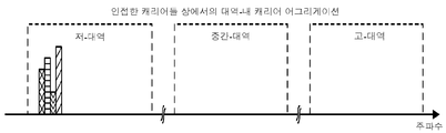
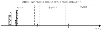
[0003] 무선 디바이스는 다수의 캐리어들 상에서의 동시적 동작인 캐리어 어그리게이션을 지원할 수 있다. 캐리어는 통신을 위해 이용되는 주파수들의 범위를 지칭할 수 있으며, 특정 특성들과 연관될 수 있다. 예를 들어, 캐리어는 캐리어 상에서의 동작을 설명하는 시스템 정보와 연관될 수 있다. 캐리어는 또한, 컴포넌트 캐리어(CC), 주파수 채널, 셀 등으로 지칭될 수 있다. 무선 디바이스에 의해 캐리어 어그리게이션을 효율적으로 지원하는 것이 바람직하다.[0003] A wireless device can support carrier aggregation, which is a concurrent operation on multiple carriers. Carriers may refer to a range of frequencies used for communication and may be associated with certain characteristics. For example, the carrier may be associated with system information describing operation on the carrier. The carrier may also be referred to as a component carrier (CC), a frequency channel, a cell, and so on. It is desirable to efficiently support carrier aggregation by the wireless device.
[0004] 도 1은 무선 시스템과 통신하는 무선 디바이스를 도시한다.
[0005] 도 2a 내지 도 2d는 캐리어 어그리게이션(CA)의 4개의 예들을 도시한다.
[0006] 도 3은 도 1의 무선 디바이스의 블록도를 도시한다.
[0007] 도 4는 잡음 분할(noise splitting)이 없는 SIMO(single-input multiple-output) LNA(low noise amplifier)를 도시한다.
[0008] 도 5는 전류 버퍼 출력에서 잡음 분할이 있는 SIMO LNA를 도시한다.
[0009] 도 6a 내지 도 7c는 전류 버퍼 출력에서 잡음 분할이 있는 SIMO LNA의 일부 예시적 설계들을 도시한다.
[0010] 도 8은 이득 회로 출력에서 잡음 분할이 있는 SIMO LNA를 도시한다.
[0011] 도 9a 내지 도 9c는 이득 회로 출력에서 잡음 분할이 있는 SIMO LNA의 일부 예시적 설계들을 도시한다.
[0012] 도 10은 신호 증폭을 수행하기 위한 프로세스를 도시한다.[0004] FIG. 1 illustrates a wireless device in communication with a wireless system.
[0005] Figures 2A-2D illustrate four examples of carrier aggregation (CA).
[0006] FIG. 3 shows a block diagram of the wireless device of FIG. 1.
[0007] FIG. 4 illustrates a single-input multiple-output (SIMO) low noise amplifier (LNA) without noise splitting.
[0008] FIG. 5 illustrates a SIMO LNA with noise division at the current buffer output.
[0009] Figures 6A-7C illustrate some exemplary designs of a SIMO LNA with noise division at the current buffer output.
[0010] FIG. 8 illustrates a SIMO LNA with noise segmentation at the gain circuit output.
[0011] Figures 9a-9c illustrate some exemplary designs of a SIMO LNA with noise division at the gain circuit output.
[0012] FIG. 10 illustrates a process for performing signal amplification.
[0013] 아래에서 설명되는 상세한 설명은 본 개시의 예시적 설계들의 설명으로서 의도되며, 본 개시가 실시될 수 있는 유일한 설계들만을 나타내는 것으로 의도되는 것은 아니다. "예시적"이라는 용어는, "예, 예시 또는 예증으로 역할을 하는"을 의미하는 것으로 본원에서 이용된다. 본원에 "예시적"으로서 설명된 임의의 설계는 반드시 다른 설계들보다 선호되거나 또는 유리한 것으로 해석되어서는 안 된다. 상세한 설명은 본 개시의 예시적 설계들의 완전한 이해를 제공하기 위해 특정 세부사항들을 포함한다. 본원에 설명된 예시적 설계들이 이러한 특정 세부사항들 없이 실시될 수 있다는 것이 당업자들에게 명백할 것이다. 일부 예시들에서, 잘 알려져 있는 구조들 및 디바이스들은 본원에 제시된 예시적 설계들의 신규성을 모호하게 하는 것을 회피하기 위해 블록도 형태로 도시된다.[0013] The following detailed description is intended as a description of exemplary designs of the present disclosure, and is not intended to represent the only designs in which the present disclosure may be practiced. The word "exemplary" is used herein to mean "serving as an example, instance, or illustration. &Quot; Any design described herein as "exemplary " is not necessarily to be construed as preferred or advantageous over other designs. The detailed description includes specific details to provide a thorough understanding of the exemplary designs of the present disclosure. It will be apparent to those skilled in the art that the exemplary designs described herein may be practiced without these specific details. In some instances, well-known structures and devices are shown in block diagram form in order to avoid obscuring the novelty of the exemplary designs presented herein.
[0014] 잡음 분할이 있고, 양호한 성능 및 다른 바람직한 특성들을 가지는 증폭기가 본원에 개시된다. 이 증폭기들은 다수의 송신된 신호들의 동시 수신을 지원하는 SIMO LNA들을 포함할 수 있다. 이 증폭기들은 다양한 타입들의 전자 디바이스들, 이를테면, 무선 통신 디바이스들에 이용될 수 있다.[0014] There is disclosed herein an amplifier having noise division, good performance and other desirable characteristics. These amplifiers may include SIMO LNAs that support simultaneous reception of multiple transmitted signals. These amplifiers can be used in various types of electronic devices, such as wireless communication devices.
[0015] 도 1은 무선 통신 시스템들(120)과 통신하는 무선 디바이스(110)를 도시한다. 무선 시스템들(120)은 LTE(Long Term Evolution) 시스템, CDMA(Code Division Multiple Access) 시스템, GSM(Global System for Mobile Communications) 시스템, WLAN(wireless local area network) 시스템 또는 일부 다른 무선 시스템일 수 있다. CDMA 시스템은 WCDMA(Wideband CDMA), CDMA 1X, EVDO(Evolution-Data Optimized), TD-SCDMA(Time Division Synchronous CDMA) 또는 CDMA의 일부 다른 버전을 구현할 수 있다. 간략성을 위해서, 도 1은 2개의 기지국들(130 및 132) 및 하나의 시스템 제어기(140)를 포함하는 무선 시스템(120)을 도시한다. 일반적으로, 무선 시스템은 많은 기지국들 및 임의의 세트의 네트워크 엔티티들을 포함할 수 있다.[0015] FIG. 1 illustrates a
[0016] 무선 디바이스(110)는 또한, UE(user equipment), 이동국, 단말, 액세스 단말, 가입자 유닛, 스테이션 등으로 지칭될 수 있다. 무선 디바이스(110)는 셀룰러 폰, 스마트폰, 태블릿, 무선 모뎀, PDA(personal digital assistant), 핸드헬드 디바이스, 랩탑 컴퓨터, 스마트북, 넷북, 코드리스 폰, WLL(wireless local loop) 스테이션, 블루투스 디바이스 등일 수 있다. 무선 디바이스(110)는 무선 시스템(120)과 통신할 수 있다. 무선 디바이스(110)는 또한, 브로드캐스트 스테이션들(예를 들어, 브로드캐스트 스테이션(134))로부터 신호들을 수신하고, 하나 또는 둘 이상의 GNSS(global navigation satellite systems)에서의 위성들(예를 들어, 위성(150))로부터 신호들을 수신하는 식으로 수신할 수 있다. 무선 디바이스(110)는 LTE, WCDMA, CDMA 1X, EVDO, TD-SCDMA, GSM, 802.11 등과 같은 무선 통신을 위한 하나 또는 둘 이상의 라디오 기술들을 지원할 수 있다.[0016] The
[0017] 무선 디바이스(110)는 다수의 캐리어들 상에서의 동작인 캐리어 어그리게이션을 지원할 수 있다. 캐리어 어그리게이션은 또한, 다중-캐리어 동작으로 지칭될 수 있다. 무선 디바이스(110)는 698 내지 960 메가헤르츠(MHz)의 저-대역, 1475 내지 2170 MHz의 중간-대역 및/또는 2300 내지 2690 MHz 그리고 3400 내지 3800 MHz의 고-대역에서 동작할 수 있다. 저-대역, 중간-대역 및 고-대역은 대역들의 3개의 그룹들(또는 대역 그룹들)을 지칭하며, 각각의 대역 그룹은 다수의 주파수 대역들(또는 간단히, "대역들")을 포함한다. 각각의 대역은 최대 200 MHz를 커버할 수 있으며, 하나 또는 둘 이상의 캐리어들을 포함할 수 있다. 각각의 캐리어는 LTE에서 최대 20 MHz를 커버할 수 있다. LTE 릴리즈 11은 35개의 대역들을 지원하는데, 이 35개의 대역들은 LTE/UMTS 대역들로 지칭되며, 3GPP TS 36.101에서 리스팅된다. 무선 디바이스(110)는 LTE 릴리즈 11에서, 1개 또는 2개의 대역들에서 최대 5개의 캐리어들로 구성될 수 있다.[0017] The
[0018] 일반적으로, 캐리어 어그리게이션(CA)은 2개의 타입들, 즉, 대역-내 CA 및 대역-간 CA로 카테고리화될 수 있다. 대역-내 CA는 동일한 대역 내에서의 다수의 캐리어들 상에서의 동작을 지칭한다. 대역-간 CA는 서로 다른 대역들에서의 다수의 캐리어들 상에서의 동작을 지칭한다.[0018] In general, carrier aggregation (CA) can be categorized into two types: intra-band CA and inter-band CA. An intra-band CA refers to operation on multiple carriers within the same band. A band-wise CA refers to operation on multiple carriers in different bands.
[0019] 도 2a는 인접한 대역-내 CA의 예를 도시한다. 도 2a에 도시된 예에서, 무선 디바이스(110)는 저-대역에서의 하나의 대역에서의 4개의 인접한 캐리어들로 구성된다. 무선 디바이스(110)는 동일한 대역 내에서의 다수의 인접한 캐리어들 상에서 송신들을 전송 및/또는 수신할 수 있다.[0019] FIG. 2A shows an example of an adjacent in-band CA. In the example shown in FIG. 2A, the
[0020] 도 2b는 인접하지 않은 대역-내 CA의 예를 도시한다. 도 2b에 도시된 예에서, 무선 디바이스(110)는 저-대역에서의 하나의 대역에서의 4개의 인접하지 않은 캐리어들로 구성된다. 캐리어들은 5 MHz, 10 MHz 또는 일부 다른 양만큼 분리될 수 있다. 무선 디바이스(110)는 동일한 대역 내에서의 다수의 인접하지 않은 캐리어들 상에서 송신들을 전송 및/또는 수신할 수 있다.[0020] FIG. 2B shows an example of non-contiguous intra-band CAs. In the example shown in FIG. 2B, the
[0021] 도 2c는 동일한 대역 그룹에서의 대역-간 CA의 예를 도시한다. 도 2c에 도시된 예에서, 무선 디바이스(110)는 저-대역에서의 2개의 대역들에서의 4개의 캐리어들로 구성된다. 무선 디바이스(110)는 동일한 대역 그룹의 서로 다른 대역들에서의 다수의 캐리어들 상에서 송신들을 전송 및/또는 수신할 수 있다.[0021] FIG. 2C shows an example of band-intervening CAs in the same band group. In the example shown in FIG. 2C, the
[0022] 도 2d는 서로 다른 대역 그룹들에서의 대역-간 CA의 예를 도시한다. 도 2d에 도시된 예에서, 무선 디바이스(110)는 서로 다른 대역 그룹들의 2개의 대역들에서의 4개의 캐리어들로 구성되는데, 이 4개의 캐리어들은 저-대역의 일 대역에서 2개의 캐리어들 및 중간-대역의 다른 대역에서 2개의 캐리어들을 포함한다. 무선 디바이스(110)는 서로 다른 대역 그룹들서의 서로 다른 대역들에서의 다수의 캐리어들 상에서 송신들을 전송 및/또는 수신할 수 있다.[0022] FIG. 2d shows an example of band-interleaved CA in different band groups. In the example shown in FIG. 2D, the
[0023] 도 2a 내지 도 2d는 캐리어 어그리게이션의 4개의 예들을 도시한다. 캐리어 어그리게이션은 또한, 대역 그룹들 및 대역들의 다른 결합들에 대해 지원될 수 있다. [0023] Figures 2A-2D illustrate four examples of carrier aggregation. Carrier aggregation may also be supported for other combinations of band groups and bands.
[0024] 도 3은 도 1의 무선 디바이스(110)의 예시적 설계의 블록도를 도시한다. 이 예시적 설계에서, 무선 디바이스(110)는 1차(primary) 안테나(310)에 커플링된 트랜시버(320), 2차(secondary) 안테나(312)에 커플링된 트랜시버(322) 및 데이터 프로세서/제어기(380)를 포함한다. 트랜시버(320)는 다수의 주파수 대역들, 다수의 라디오 기술들, 캐리어 어그리게이션 등을 지원하기 위해 다수(K개)의 수신기들(330pa 내지 330pk) 및 다수(K개)의 송신기들(350pa 내지 350pk)을 포함한다. 트랜시버(322)는 다수의 주파수 대역들, 다수의 라디오 기술들, 캐리어 어그리게이션, 수신 다이버시티, 다수의 송신 안테나들로부터 다수의 수신 안테나들로의 MIMO(multiple-input multiple-output) 송신 등을 지원하기 위해 L개의 수신기들(330sa 내지 330sl) 및 L개의 송신기들(350sa 내지 350sl)을 포함한다.[0024] FIG. 3 shows a block diagram of an exemplary design of the
[0025] 도 3에 도시된 예시적 설계에서, 각각의 수신기(330)는 LNA(340) 및 수신 회로들(342)을 포함한다. 데이터 수신을 위해, 안테나(310)는 기지국들 및/또는 다른 송신기 스테이션들로부터 신호들을 수신하고, 수신된 RF 신호를 제공하며, 이 수신된 RF 신호는 안테나 인터페이스 회로(324)를 통해 라우팅되며, 입력 RF 신호로서 선택된 수신기에 제공된다. 안테나 인터페이스 회로(324)는 스위치들, 듀플렉서들, 송신 필터들, 수신 필터들, 매칭 회로들 등을 포함할 수 있다. 아래의 설명은 수신기(330pa)가 선택된 수신기라고 가정한다. 수신기(330pa) 내에서, LNA(340pa)는 입력 RF 신호를 증폭시키며, 출력 RF 신호를 제공한다. 수신 회로들(342pa)은 RF로부터 기저대역으로 출력 RF 신호를 하향변환하고, 하향변환된 신호를 증폭시켜 필터링하며, 아날로그 입력 신호를 데이터 프로세서(380)에 제공한다. 수신 회로들(342pa)은 믹서들, 필터들, 증폭기들, 매칭 회로들, 발진기, LO(local oscillator) 생성기, PLL(phase locked loop) 등을 포함할 수 있다. 트랜시버들(320 및 322) 내의 각각의 나머지 수신기(330)는 수신기(330pa)와 유사한 방식으로 동작할 수 있다.[0025] In the exemplary design shown in FIG. 3, each receiver 330 includes an LNA 340 and receive circuits 342. For data reception,
[0026] 도 3에 도시된 예시적 설계에서, 각각의 송신기(350)는 송신 회로들(352) 및 전력 증폭기(PA)(354)를 포함한다. 데이터 송신을 위해, 데이터 프로세서(380)는 송신될 데이터를 프로세싱(예를 들어, 인코딩 및 변조)하며, 아날로그 출력 신호를 선택된 송신기에 제공한다. 아래의 설명은 송신기(350pa)가 선택된 송신기라고 가정한다. 송신기(350pa) 내에서, 송신 회로들(352pa)은 아날로그 출력 신호를 증폭시키고 필터링하여 기저대역으로부터 RF로 상향변환하여, 변조된 RF 신호를 제공한다. 송신 회로들(352pa)은 증폭기들, 필터들, 믹서들, 매칭 회로들, 발진기, LO 생성기, PLL 등을 포함할 수 있다. PA(354pa)는 변조된 RF 신호를 수신하여 증폭시켜, 적절한 출력 전력 레벨을 가지는 송신 RF 신호를 제공한다. 송신 RF 신호는 안테나 인터페이스 회로(324)를 통해 라우팅되며, 안테나(310)를 통해 송신된다. 트랜시버들(320 및 322) 내의 각각의 나머지 송신기(350)는 송신기(350pa)와 유사한 방식으로 동작할 수 있다.[0026] In the exemplary design shown in FIG. 3, each transmitter 350 includes transmit circuits 352 and a power amplifier (PA) 354. For data transmission, a
[0027] 도 3은 수신기들(330) 및 송신기들(350)의 예시적 설계를 도시한다. 수신기 및 송신기는 또한, 도 3에 도시되지 않은 다른 회로들, 이를테면, 필터들, 매칭 회로들 등을 포함할 수 있다. 트랜시버들(320 및 322) 전부 또는 일부가 하나 또는 둘 이상의 아날로그 집적 회로(IC)들, RF IC(RFIC)들, 믹싱된-신호 IC들 등에 구현될 수 있다. 예를 들어, LNA들(340) 및 수신 회로들(342)은, RFIC일 수 있는 하나의 모듈에 구현되는 식으로 구현될 수 있다. 트랜시버들(320 및 322) 내의 회로들은 또한, 다른 방식들로 구현될 수 있다.[0027] FIG. 3 illustrates an exemplary design of receivers 330 and transmitters 350. The receiver and transmitter may also include other circuits not shown in Fig. 3, such as filters, matching circuits, and the like. All or a portion of the
[0028] 데이터 프로세서/제어기(380)는 무선 디바이스(110)에 대한 다양한 기능들을 수행할 수 있다. 예를 들어, 데이터 프로세서(380)는 수신기들(330)을 통해 수신되는 데이터 및 송신기들(350)을 통해 송신되는 데이터에 대한 프로세싱을 수행할 수 있다. 제어기(380)는 트랜시버들(320 및 322) 내의 다양한 회로들의 동작을 제어할 수 있다. 메모리(382)는 데이터 프로세서/제어기(380)에 대한 프로그램 코드들 및 데이터를 저장할 수 있다. 데이터 프로세서/제어기(380)가 하나 또는 둘 이상의 ASIC(application specific integrated circuit)들 및/또는 다른 IC들 상에 구현될 수 있다.[0028] Data processor /
[0029] 무선 디바이스(110)는 하나 또는 둘 이상의 SIMO LNA들을 포함할 수 있다. SIMO LNA는 단일 입력 및 다수(M)개의 출력들을 포함하며, 자신의 입력에서 단일 입력 RF 신호를 수신할 수 있고, 최대 M개의 출력들로부터의 최대 M개의 출력 RF 신호들을 제공할 수 있다. SIMO LNA는 (i) 대역-내 CA에 대한 동일한 대역에서 다수의 캐리어들 상에서 전송된 다수의 송신들 또는 (ii) 서로 다른 무선 시스템들(예를 들어, LTE 및 WCDMA)로부터의 다수의 송신된 신호들을 동시에 수신하기 위해 이용될 수 있다. [0029] The
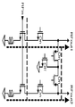
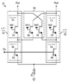
[0030] 도 4는 잡음 분할이 없는 SIMO LNA(440)의 예시적 설계의 블록도를 도시한다. SIMO LNA(440)는 M개의 부하 회로들(490a 내지 490m)에 커플링된 다수(M)개의 증폭기 회로들(450a 내지 450m)을 각각 포함한다. 모든 M개의 증폭기 회로들(450a 내지 450m)의 입력들은 함께 커플링된다. 각각의 증폭기 회로(450)는 전류 버퍼(470)에 커플링된 이득 회로(460)를 포함한다. 각각의 증폭기 회로(450)는 각각의 Venb 제어 신호를 통해 자신의 전류 버퍼(470)를 턴온함으로써 인에이블될 수 있다.[0030] FIG. 4 shows a block diagram of an exemplary design of a
[0031] 입력 RF 신호(RFin)는 M개의 증폭기 회로들(450a 내지 450m)에 인가될 수 있다. 하나 또는 둘 이상의 증폭기 회로들(450)은 연관된 전류 버퍼들(470)을 턴온함으로써 인에이블될 수 있다. 예를 들어, N개의 증폭기 회로들(450)은 대역-내 CA에 대해 동일한 대역의 캐리어들의 N개의 세트들 상에서의 송신들을 동시에 수신하도록 인에이블될 수 있으며, 여기서, 1 ≤N≤M이다. 캐리어들의 각각의 세트는 하나 또는 둘 이상의 캐리어들을 포함할 수 있다. 각각의 인에이블되는 증폭기 회로(450)는 입력 RF 신호를 증폭시키고, 출력 RF 신호를 그것의 부하 회로(490)에 제공할 수 있다.[0031] The input RF signal RFin may be applied to the
[0032] SIMO LNA(440) 내의 N개의 인에이블되는 증폭기 회로들(450)은 독립적으로 동작하며, 프로세싱되는 신호들 또는 서로 다른 송신들 사이에 격리(isolation)를 제공하기 위해 서로 분리되는 출력들을 가진다. 각각의 이득 회로(460)는 ![]()
![]()
![]()
![]()
[0033] 본 개시의 양상에서, 잡음 분할이 있는 SIMO LNA는 다수의 송신들 또는 신호들의 동시 수신을 지원하기 위해 이용될 수 있다. 잡음 분할은, 각각의 출력이 더 적은 잡음을 관측하며 더 양호한/더 낮은 잡음 피겨를 달성할 수 있도록, 다중 출력들 사이에서의 잡음의 "분할"을 지칭한다. [0033] In an aspect of the present disclosure, a SIMO LNA with noise partitioning may be used to support simultaneous reception of multiple transmissions or signals. Noise partitioning refers to the "division" of noise between multiple outputs so that each output can observe less noise and achieve a better / lower noise figure.
[0034] 도 5는 전류 버퍼 출력에서의 잡음 분할이 있는 SIMO LNA(540)의 예시적 설계의 블록도를 도시한다. SIMO LNA(540)는 도 3의 하나 또는 둘 이상의 LNA들(340)에 대해 이용될 수 있다. SIMO LNA(540)는 M개의 부하 회로들(590a 내지 590m)에 커플링된 다수(M)개의 증폭기 회로들(550a 내지 550m)를 각각 포함한다. 각각의 증폭기 회로(550)는 전류 버퍼(570)에 커플링된 이득 회로(560)를 포함한다. 각각의 증폭기 회로(550)는 각각의 Venb 제어 신호를 통해 자신의 전류 버퍼(570)를 턴온함으로써 인에이블될 수 있다.[0034] FIG. 5 shows a block diagram of an exemplary design of a
[0035] 도 5에 도시된 예시적 설계에서, SIMO LNA(540)는 증폭기 회로들(550)의 출력들 사이에 커플링된 상호연결 회로들(580)을 더 포함한다. 각각의 상호연결 회로(580)는 (도 5에 도시된 바와 같은) 스위치(582)로 또는 일부 다른 회로로 구현될 수 있다. 각각의 스위치(582)는 (i) 스위치에 커플링된 2개의 증폭기 회로들(550)을 격리하기 위해 개방되거나 (ii) 2개의 증폭기 회로들(550)의 출력들을 연결시키고 이 증폭기 회로들로부터의 출력 전류들을 가산(sum)하기 위해 폐쇄될 수 있다.[0035] In the exemplary design shown in FIG. 5, the
[0036] 일반적으로, 임의의 수의 증폭기 회로들(550) 및 증폭기 회로들(550) 중 어느 하나는 임의의 주어진 순간에 인에이블될 수 있다. 게다가, 임의의 수의 스위치들(582) 및 스위치들(582) 중 어느 하나는 임의의 주어진 순간에 폐쇄될 수 있다. 주어진 증폭기 회로(550)는 자체적으로 그것의 부하 회로(590)를 구동시킬 수 있다. 대안적으로, 다수의 증폭기 회로들(550)은 자신들의 출력들이 자신들의 폐쇄된 스위치들(582)을 통해 함께 커플링되게 할 수 있으며, 이들의 부하 회로들(590)을 집합적으로 구동시킬 수 있다. 자신들의 출력들이 함께 커플링되게 하는 증폭기 회로들(550)의 잡음 피겨들은 잡음 분할을 통해 개선될 수 있다.[0036] In general, any one of any number of amplifier circuits 550 and amplifier circuits 550 may be enabled at any given moment. In addition, any one of the switches 582 and switches 582 may be closed at any given moment. A given amplifier circuit 550 may itself drive its load circuit 590. Alternatively, multiple amplifier circuits 550 may cause their outputs to be coupled together via their closed switches 582, and may be used to collectively drive their load circuits 590 . The noise figures of the amplifier circuits 550 that cause their outputs to be coupled together can be improved through noise partitioning.
[0037] 모든 스위치들(582)이 개방되면, 각각의 증폭기 회로(550)는 단지 그것의 부하 회로(590)만을 구동시킬 수 있다. 각각의 증폭기 회로(550)에 의해 그것의 부하 회로(590)에 제공되는 출력 전류는 다음과 같이 표현될 수 있다:[0037] When all the switches 582 are open, each amplifier circuit 550 can only drive its load circuit 590 only. The output current provided by its respective amplifier circuit 550 to its load circuit 590 can be expressed as:
![]()
![]()
여기서, ![]()
![]()
![]()
![]()
![]()
![]()
[0038] 각각의 부하 회로(590)에서의 잡음 전력은 다음과 같이 표현될 수 있다:[0038] The noise power at each load circuit 590 can be expressed as:
![]()
![]()
여기서, ![]()
![]()
![]()
![]()
[0039] 모든 스위치들(582)이 폐쇄되면, 모든 M개의 증폭기 회로들(550a 내지 550m)의 출력들은 가산 노드(summing node) X에서 함께 쇼트된다. 이러한 경우, 가산 노드에서의 총 전류 itotal은 다음과 같이 표현될 수 있다:When all the switches 582 are closed, the outputs of all the

여기서, ![]()
![]()
![]()
![]()
[0040] M개의 증폭기 회로들(550a 내지 550m)로부터의(또는 더 구체적으로, M개의 이득 회로들(560a 내지 560m)로부터의) 신호 전류들(![]()
![]()
![]()
![]()
![]()
![]()
![]()
![]()
![]()
![]()
[0041] 가산 노드에서의 총 전류는 분할되어, M개의 부하 회로들(590a 내지 590m)에 제공될 수 있다. 각각의 부하 회로(590)에 의해 수신된 전류는 다음과 같이 표현될 수 있다:[0041] The total current at the adder node may be divided and provided to M load circuits 590a through 590m. The current received by each load circuit 590 can be expressed as: < RTI ID = 0.0 >

여기서, ![]()
![]()
[0042] M개의 증폭기 회로들(550a 내지 550m)로부터의 잡음 전류들은 상관되지 않아야 하고, 보강적으로 또는 상쇄적으로 더해질 수 있다. 따라서, 각각의 부하 회로(590)에서의 잡음 전력은 다음과 같이 표현될 수 있다:[0042] Noise currents from the

여기서, ![]()
![]()
![]()
![]()
[0043] 수식들(2) 및 (5)에 도시된 바와 같이, 잡음 분할은 M배만큼 각각의 부하 회로(590)에서의 잡음 전력을 감소시킬 수 있는데, M은 자신들의 출력들이 함께 쇼트되게 하는 증폭기 회로들(550)의 수에 대응한다. 잡음 전력의 감소는 상관되지 않는 M개의 증폭기 회로들(550a 내지 550m)로부터의 잡음 전류들로 인한 것이다. 각각의 부하 회로(590)에서의 신호 전력은 증폭기 회로들(550)의 출력들이 함께 쇼트되는지 아닌지에 관계없이 대략 동일할 수 있다. 잡음 분할이 있거나 잡음 분할이 없는 일정한 신호 전력은, 유사하거나 높게 상관되는 M개의 증폭기 회로들(550a 내지 550m)로부터의 신호 전류들로 인한 것이다. 신호 전력은 대략 동일한 반면, 잡음 전력은 잡음 분할에 의해 M배 감소되기 때문에, 각각의 부하 회로(590)에서의 잡음 피겨는 잡음 분할에 의해 개선될 수 있다.As shown in equations (2) and (5), the noise division can reduce the noise power in each load circuit 590 by M times, where M is the sum of their outputs together Gt; 550 < / RTI > The reduction in noise power is due to the noise currents from the unmistakable
[0044] 전류 버퍼 출력에서의 잡음 분할이 있는 SIMO LNA(540)는 다양한 회로 아키텍처들로 구현될 수 있다. SIMO LNA(540)의 일부 예시적 설계들은 아래에서 설명된다. SIMO LNA(540)는 또한, 다양한 타입들의 트랜지스터들로 구현될 수 있다. NMOS(N-channel metal oxide semiconductor) 트랜지스터들로 구현되는 SIMO LNA(540)의 일부 예시적 설계들은 아래에서 설명된다.[0044] The
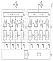
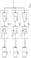
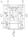
[0045] 도 6a는 전류 버퍼 출력에서 별개의 유도성 디제너레이션(inductive degeneration) 및 잡음 분할이 있는 SIMO LNA(640a)의 예시적 설계의 개략도를 도시한다. SIMO LNA(640a)는 도 5의 SIMO LNA(540)의 일 예시적 설계이다. SIMO LNA(640a)는 2개의 증폭기 회로들(650a 및 650b) 및 스위치(682a)를 포함한다. 각각의 증폭기 회로(650)는 이득 회로(660) 및 전류 버퍼(670)를 포함한다. SIMO LNA(640a)는 입력 RF 신호를 수신하고, 입력 RF 신호는 증폭기 회로들(650a 및 650b) 둘 모두에 인가된다. 입력 RF 신호는 캐리어 어그리게이션을 위한, 캐리어들의 하나 또는 두 세트들 상에서의 송신들을 포함할 수 있는데, 각각의 세트는 하나 또는 둘 이상의 캐리어들을 포함한다. 대안적으로, 입력 RF 신호는 동시에 수신될 (예를 들어, 2개의 무선 시스템들로부터의) 2개의 송신된 신호들을 포함할 수 있다.[0045] FIG. 6a shows a schematic diagram of an exemplary design of a
[0046] 도 6a에 도시된 예시적 설계에서, 각각의 이득 회로(660)는 이득 트랜지스터(664) 및 소스 디제너레이션 인덕터(666)를 포함한다. 이득 회로(660a) 내에서, 이득 트랜지스터(664a)는 입력 RF 신호를 수신하는 그것의 게이트를 가지고, 그것의 소스는 인덕터(666a)의 한 종단에 커플링되고, 그것의 드레인은 이득 회로(660a)의 출력을 형성한다. 인덕터(666a)의 다른 종단은 회로 접지에 커플링된다. 도 6a에 도시된 예시적 설계에서, 각각의 전류 버퍼(670)는 캐스코드 트랜지스터(674)를 포함한다. 전류 버퍼(670a) 내에서, 캐스코드 트랜지스터(674a)는, 전류 버퍼(670a)의 입력을 형성하고 이득 트랜지스터(664a)의 드레인에 커플링되는 그것의 소스, Venb1 제어 신호를 수신하는 그것의 게이트, 및 전류 버퍼(670a)의 출력을 형성하고 부하 회로(690a)에 커플링되는 그것의 드레인을 가진다. 증폭기 회로(650b)는 이득 트랜지스터(664b), 소스 디제너레이션 인덕터(666b) 및 캐스코드 트랜지스터(674b)를 포함하고, 이들은 증폭기 회로(650a) 내의 이득 트랜지스터(664a), 인덕터(666a) 및 캐스코드 트랜지스터(674a)와 유사한 방식으로 커플링된다. 이득 트랜지스터들(664) 및 캐스코드 트랜지스터들(674)은 도 6a에 도시된 바와 같이, NMOS 트랜지스터들로 또는 다른 타입들의 트랜지스터들로 구현될 수 있다.[0046] In the exemplary design shown in FIG. 6A, each gain circuit 660 includes a gain transistor 664 and a source degeneration inductor 666. Within
[0047] 도 6a에 도시된 예시적 설계에서, 스위치(682a)는 NMOS 트랜지스터들(684a, 684b 및 686)을 포함한다. NMOS 트랜지스터(684a)는 노드 A에 커플링된 그것의 드레인, Sw 제어 신호를 수신하는 그것의 게이트 및 전류 버퍼(670a)의 출력인 캐스코드 트랜지스터(674a)의 드레인에 커플링된 그것의 소스를 가진다. NMOS 트랜지스터(684b)는 노드 A에 커플링된 그것의 드레인, Sw 제어 신호를 수신하는 그것의 게이트 및 전류 버퍼(670b)의 출력인 캐스코드 트랜지스터(674b)의 드레인에 커플링된 그것의 소스를 가진다. NMOS 트랜지스터(686)는 노드 A에 커플링된 그것의 드레인, ![]()
![]()
![]()
![]()
![]()
![]()
![]()
![]()
[0048] 증폭기 회로들(650a 및 650b)은 또한, 다른 방식들로 구현될 수 있다. 또 다른 예시적 설계에서, 증폭기 회로는 (소스 디제너레이션 인덕터 대신에) 회로 접지에 직접 커플링된 그것의 소스를 가지는 이득 트랜지스터를 포함할 수 있다. 또 다른 예시적 설계에서, 증폭기 회로는, 병렬로 커플링되고 입력 RF 신호를 수신하는 이들의 게이트들을 가지는 2개의 이득 트랜지스터들을 포함할 수 있다. 제 1 이득 트랜지스터는 도 6a에 도시된 바와 같이, 소스 디제너레이션 인덕터에 커플링된 그것의 소스를 가질 수 있다. 제 2 이득 트랜지스터는 회로 접지에 직접 커플링된 그것의 소스를 가질 수 있다. 제 1 또는 제 2 이득 트랜지스터는 입력 RF 신호의 수신된 전력에 의존하여 선택될 수 있다. [0048] The
[0049] 도 6a에 도시된 예시적 설계에서, 각각의 부하 회로(690)는 1차 코일(694) 및 2차 코일(696)을 포함하는 트랜스포머(692)를 포함한다. 코일은 또한, 인덕터 코일, 와인딩(winding), 컨덕터 등으로 지칭될 수 있다. 부하 회로(690a) 내에서, 트랜스포머(692a)는 (i) 증폭기 회로(650a)의 출력과 파워 서플라이(VDD) 사이에 커플링된 1차 코일(694a) 및 (ii) 제 1 차동 증폭 RF 신호를 제 1 다운컨버터(도 6a에 도시되지 않음)에 제공하는 2차 코일(696a)을 포함한다. 부하 회로(690b)는 (i) 증폭기 회로(650b)의 출력과 VDD 서플라이 사이에 커플링된 1차 코일(694b) 및 (ii) 제 2 차동 증폭 RF 신호를 제 2 다운컨버터(도 6a에 도시되지 않음)에 제공하는 2차 코일(696b)을 가지는 트랜스포머(692b)를 포함한다. 각각의 다운컨버터는 RF로부터 기저대역 또는 중간 주파수로의 증폭 RF 신호의 쿼드러처 다운컨버전(quadrature downconversion)을 수행하기 위한 2개의 믹서들을 포함할 수 있다.6A, each load circuit 690 includes a transformer 692 that includes a primary coil 694 and a secondary coil 696. The transformer 692 includes a primary coil 694 and a secondary coil 696, The coils may also be referred to as inductor coils, windings, conductors, and the like. Within load circuit 690a,
[0050] 부하 회로들(690)은 또한, 다른 방식들로 구현될 수 있다. 또 다른 예시적 설계에서, 부하 회로는 증폭기 회로의 출력과 VDD 서플라이 사이에 커플링된 인덕터 및 가능하게는 캐패시터를 포함할 수 있다. 또 다른 예시적 설계에서, 부하 회로는, VDD 서플라이에 커플링된 그것의 소스 및 캐스코드 트랜지스터(674)의 드레인에 커플링된 그것의 드레인을 가지는 PMOS(P-channel metal oxide semiconductor) 트랜지스터를 포함할 수 있다. PMOS 트랜지스터는 캐스코드 트랜지스터(674)에 대한 액티브 부하를 제공할 수 있다. [0050] The load circuits 690 may also be implemented in other manners. In another exemplary design, the load circuit may include an inductor and possibly a capacitor coupled between the output of the amplifier circuit and the VDD supply. In another exemplary design, the load circuit includes a PMOS (P-channel metal oxide semiconductor) transistor having its source coupled to the VDD supply and its drain coupled to the drain of the cascode transistor 674 can do. The PMOS transistor may provide an active load for the cascode transistor 674. [
[0051] 간략화를 위해, 도 6a는 2개의 부하 회로들(690a 및 690b)에 커플링된 2개의 증폭기 회로들(650a 및 650b)을 포함하는 SIMO LNA(640a)를 도시한다. SIMO LNA(640a)는 2개 초과의 부하 회로들(690)에 커플링된 2개 초과의 증폭기 회로들(650)을 포함할 수 있다.[0051] For simplicity, FIG. 6a illustrates a
[0052] SIMO LNA(640a)는 단일-출력 모드 또는 다중-출력 모드에서 동작할 수 있다. 단일-출력 모드에서, SIMO LNA(640a)는 입력 RF 신호를 수신하며, 하나의 출력 RF 신호를 하나의 부하 회로(690)에 제공한다. 단일-출력 모드는 (i) 캐리어 어그리게이션을 이용하지 않는 하나의 캐리어 상에서의 송신, 또는 (ii) 대역-간 CA에 대한 서로 다른 대역들에서의 캐리어들의 다수의 세트들 상에서의 송신들 중 한 세트의 캐리어들 상에서의 송신, 또는 (iii) 하나의 무선 시스템으로부터 송신된 신호를 수신하는데 이용될 수 있다. 다중-출력 모드에서, SIMO LNA(640a)는 입력 RF 신호를 수신하며, 2개의 출력 RF 신호들을 2개의 부하 회로들(690)에 제공한다. 다중-출력 모드는 (i) 대역-내 CA에 대한 캐리어들의 2개의 세트들 상에서의 송신들 또는 (ii) 2개의 무선 시스템들로부터 2개의 송신된 신호들을 수신하는데 이용될 수 있다. [0052] The
[0053] 도 6b는 RFout1이 인에이블되는 단일-출력 모드에서의 SIMO LNA(640a)의 동작을 도시한다. 이러한 경우, 캐스코드 트랜지스터(674a)는 턴온되고, 캐스코드 트랜지스터(674b)는 턴오프된다. 게다가, 스위치(682a)는, 트랜지스터들(684a 및 684b)을 턴오프하고 트랜지스터(686)를 턴온함으로써 개방된다. 증폭기 회로(650a)는 입력 RF 신호를 증폭시키며, 제 1 출력 RF 신호(RFout1)를 제공한다. 증폭기 회로(650a)는 개방된 스위치(682a)를 통해 증폭기 회로(650b)로부터 격리된다.[0053] FIG. 6b illustrates the operation of the
[0054] 도 6c는 RFout2가 인에이블되는 단일-출력 모드에서의 SIMO LNA(640a)의 동작을 도시한다. 이러한 경우, 캐스코드 트랜지스터(674b)는 턴온되고, 캐스코드 트랜지스터(674a)는 턴오프되며, 스위치(682a)는 개방된다. 증폭기 회로(650b)는 입력 RF 신호를 증폭시키며, 제 2 출력 RF 신호(RFout2)를 제공한다. 증폭기 회로(650b)는 개방된 스위치(682a)를 통해 증폭기 회로(650a)로부터 격리된다.[0054] FIG. 6C illustrates the operation of
[0055] 도 6d는 다중-출력 모드에서의 SIMO LNA(640a)의 동작을 도시한다. 이러한 경우, 캐스코드 트랜지스터들(674a 및 674b) 둘 모두는 턴온된다. 게다가, 스위치(682a)는, 트랜지스터들(684a 및 684b)을 턴온하고 트랜지스터(686)를 턴오프함으로써 폐쇄된다. 증폭기 회로들(650a 및 650b)은 입력 RF 신호를 증폭시키고, 이들의 출력 전류들은 가산된다. 총 전류의 대략 절반은 RFout1 신호로서 제공된다. 나머지 전류는 RFout2 신호로서 제공된다.[0055] FIG. 6D illustrates the operation of the
[0056] 도 7a는 전류 버퍼 출력에서 별개의 유도성 디제너레이션 및 잡음 분할이 있는 SIMO LNA(640b)의 예시적 설계의 개략도를 도시한다. SIMO LNA(640b)는 도 5의 SIMO LNA(540)의 또 다른 예시적 설계이다. SIMO LNA(640b)는 2개의 증폭기 회로들(650a 및 650b) 및 스위치(682b)를 포함한다. 각각의 증폭기 회로(650)는 (i) 이득 트랜지스터(664) 및 소스 디제너레이션 인덕터(666)를 포함하는 이득 회로(660) 및 (ii) 캐스코드 트랜지스터(674)를 포함하는 전류 버퍼(670)를 포함한다. 스위치(682b)는 증폭기 회로(650a)의 출력에 커플링된 그것의 소스, Sw 제어 신호를 수신하는 그것의 게이트 및 증폭기 회로(650b)의 출력에 커플링된 그것의 드레인을 가지는 NMOS 트랜지스터(688)를 포함한다. MOS 트랜지스터(예를 들어, NMOS 트랜지스터(688))는 대칭적 구조로 구현될 수 있고, MOS 트랜지스터의 소스 및 드레인은 상호교환가능할 수 있다. SIMO LNA(640b)는 도 6b 내지 도 6d에 대해 위에서 설명된 바와 같이, 단일-출력 모드 또는 다중-출력 모드에서 동작할 수 있다.[0056] FIG. 7a shows a schematic diagram of an exemplary design of a SIMO LNA 640b with separate inductive degreasing and noise segmentation at the current buffer output. The SIMO LNA 640b is another exemplary design of the
[0057] 도 6a 및 도 7a는 2개의 증폭기 회로들의 출력들을 쇼트시키는데 이용될 수 있는 스위치의 2개의 예시적 설계들을 도시한다. 스위치는 또한, 다른 방식들로 구현될 수 있다. 또 다른 예시적 설계에서, 캐패시터 및/또는 레지스터는 하나 또는 둘 이상의 MOS 트랜지스터들과 직렬로 커플링될 수 있고, 이러한 직렬 결합은 2개의 증폭기 회로들의 출력들 사이에 커플링될 수 있다. 캐패시터 및/또는 레지스터는 잡음 피겨에서의 트레이드오프를 이용하여 격리를 개선할 수 있다.[0057] Figures 6a and 7a show two exemplary designs of switches that can be used to short the outputs of two amplifier circuits. The switch may also be implemented in other manners. In another exemplary design, the capacitor and / or resistor may be coupled in series with one or more MOS transistors, and such a series combination may be coupled between the outputs of the two amplifier circuits. Capacitors and / or resistors can improve isolation using trade-offs in noise figures.
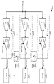
[0058] 도 7b는 전류 버퍼 출력에서 공유되는 유도성 디제너레이션 및 잡음 분할이 있는 SIMO LNA(640c)의 예시적 설계의 개략도를 도시한다. SIMO LNA(640c)는 도 5의 SIMO LNA(540)의 또 다른 예시적 설계이다. SIMO LNA(640c)는 2개의 증폭기 회로들(652a 및 652b) 및 스위치(682a)를 포함한다. 각각의 증폭기 회로(652)는 (i) 이득 트랜지스터(664)를 포함하는 이득 회로(662) 및 (ii) 캐스코드 트랜지스터(674)를 포함하는 전류 버퍼(670)를 포함한다. 이득 회로들(662a 및 662b) 내의 이득 트랜지스터들(664a 및 664b)은 이득 트랜지스터들(664a 및 664b)의 소스들에 커플링된 한 종단 및 회로 접지에 커플링된 다른 종단을 가지는 소스 디제너레이션 인덕터(666)를 공유한다. SIMO LNA(640c)는 도 6b 내지 도 6d에 대해 위에서 설명된 바와 같이, 단일-출력 모드 또는 다중-출력 모드에서 동작할 수 있다.[0058] FIG. 7b shows a schematic diagram of an exemplary design of a
[0059] 도 7c는 전류 버퍼 출력에서 잡음 분할이 있는 SIMO LNA(640c) 및 트랜스포머-기반 신호 분할이 있는 부하 회로(691)의 예시적 설계의 개략도를 도시한다. SIMO LNA(640c)는 소스 디제너레이션 인덕터(666)뿐만 아니라 스위치(682a)를 공유하는 2개의 증폭기 회로들(652a 및 652b)을 포함하고, 이들은 도 7b에 설명된 바와 같이 커플링된다. 부하 회로(691)는 증폭기 회로들(652a 및 652b)에 커플링된다. 도 7c에 도시된 예시적 설계에서, 부하 회로(691)는 1차 코일(693) 및 2개의 2차 코일들(695a 및 695b)을 가지는 트랜스포머를 포함한다. 1차 코일(693)은 증폭기 회로(652a)의 출력에 커플링된 하나의 종단, 증폭기 회로(652b)의 출력에 커플링된 다른 종단 및 VDD 서플라이에 커플링된 센터 탭(center tap)을 가진다. 2차 코일들(695a 및 695b)은 1차 코일(693)에 자기적으로 커플링된다. 2차 코일(695a)은 제 1 차동 증폭 RF 신호를 제 1 다운컨버터에 제공한다. 2차 코일(695b)은 제 2 차동 증폭 RF 신호를 제 2 다운컨버터에 제공한다. 예시적 설계에서, 2차 코일들(695a 및 695b)은 서로에 관해 대칭적일 수 있다.[0059] FIG. 7C shows a schematic diagram of an exemplary design of a
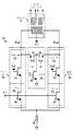
[0060] 도 8은 이득 회로 출력에서 잡음 분할이 있는 SIMO LNA(840)의 예시적 설계의 블록도를 도시한다. SIMO LNA(840)는 도 3의 하나 또는 둘 이상의 LNA들(340)에 대해 이용될 수 있다. SIMO LNA(840)는 M개의 부하 회로들(890a 내지 890m)에 각각 커플링되는 다수(M개)의 증폭기 회로들(850a 내지 850m)을 포함한다. 각각의 증폭기 회로(850)는 전류 버퍼(870)에 커플링된 이득 회로(860)를 포함한다. 각각의 증폭기 회로(850)는 각각의 Venb 제어 신호를 통해 그것의 전류 버퍼(870)를 턴온함으로써 인에이블될 수 있다.[0060] FIG. 8 shows a block diagram of an exemplary design of a
[0061] 도 8에 도시된 예시적 설계에서, SIMO LNA(840)는 이득 회로들(860)의 출력들 사이의 상호연결 회로들(880)을 더 포함한다. 상호연결 회로들(880)은 모든 인에이블되는 이득 회로들(860)로부터의 출력 전류들이 함께 가산되게 한다. 그 다음, 모든 인에이블되는 이득 회로들(860)로부터의 총 전류는 모든 인에이블되는 증폭기 회로들(850)의 전류 버퍼들(870) 사이에서 분할될 수 있다. 상호연결 회로들(880)은 아래에서 설명되는 바와 같은 다양한 방식들로 구현될 수 있다.[0061] In the exemplary design shown in FIG. 8, the
[0062] 이득 회로 출력에서 잡음 분할이 있는 SIMO LNA(840)는 다양한 회로 아키텍처들 및 다양한 타입들의 트랜지스터들로 구현될 수 있다. NMOS 트랜지스터들로 구현되는 SIMO LNA(840)의 일부 예시적 설계들이 아래에서 설명된다.[0062] The
[0063] 도 9a는 이득 회로 출력에서 별개의 유도성 디제너레이션 및 잡음 분할이 있는 SIMO LNA(940a)의 예시적 설계의 개략도를 도시한다. SIMO LNA(940a)는 도 8의 SIMO LNA(840)의 일 예시적 설계이다. SIMO LNA(940a)는 2개의 증폭기 회로들(950a 및 950b), 및 AC 커플링 캐패시터(982)로 구현되는 상호연결 회로(980a)를 포함한다. 각각의 증폭기 회로(950)는 (i) 이득 트랜지스터(964) 및 소스 디제너레이션 인덕터(966)를 포함하는 이득 회로(960) 및 (ii) 캐스코드 트랜지스터(974)를 포함하는 전류 버퍼(970)를 포함한다. 캐패시터(982)는 이득 회로들(960a 및 960b)의 출력들 사이에 커플링되며, 이득 회로들(960a 및 960b)의 출력들을 전기적으로 쇼트시키도록 작동한다. 전류 버퍼들(970a 및 970b)이 격리를 제공할 수 있기 때문에, 이득 회로들(960)의 출력들은 스위치들을 이용할 필요성 없이, 캐패시터(982)를 통해 함께 효과적으로 쇼트될 수 있다. SIMO LNA(940a)는 입력 RF 신호를 수신하는데, 이는 증폭기 회로들(950a 및 950b) 둘 모두에 인가된다. 증폭기 회로들(950a 및 950b)은 2개의 출력 RF 신호들(RFout1 및 RFout2)을 각각 제공한다.[0063] FIG. 9a shows a schematic diagram of an exemplary design of a
[0064] 도 9a는 상호연결 회로(980a)가 캐패시터(982)로 구현되는 예시적 설계를 도시한다. 캐패시터(982)는 그것의 임피던스가 캐스코드 트랜지스터들(974)의 트랜스컨덕턴스(또는 1/gm)에 비해 작도록 충분히 커야한다. 상호연결 회로는 또한, 다른 회로들과 다른 방식들로 구현될 수 있다.[0064] FIG. 9A illustrates an exemplary design in which
[0065] SIMO LNA(940a)는 단일-출력 모드 또는 다중-출력 모드에서 동작할 수 있다. 단일-출력 모드에서, SIMO LNA(940a)는 입력 RF 신호를 수신하며, RFout1 또는 RFout2일 수 있는 하나의 출력 RF 신호를 제공한다. 다중-출력 모드에서, SIMO LNA(940a)는 입력 RF 신호를 수신하며, 2개의 출력 RF 신호들(RFout1 및 RFout2)을 제공한다.[0065] The
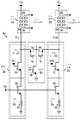
[0066] 도 9b는 이득 회로 출력에서 공유된 유도성 디제너레이션 및 잡음 분할이 있는 SIMO LNA(940b)의 예시적 설계의 개략도를 도시한다. SIMO LNA(940b)는 도 8의 SIMO LNA(840)의 또 다른 예시적 설계이다. SIMO LNA(940b)는 2개의 증폭기 회로들(952a 및 952b) 및 상호연결 회로(980a)를 포함한다. 각각의 증폭기 회로(952)는 (i) 이득 트랜지스터(964)를 포함하는 이득 회로(962) 및 (ii) 캐스코드 트랜지스터(974)를 포함하는 전류 버퍼(970)를 포함한다. 이득 회로들(962a 및 962b) 내의 이득 트랜지스터들(964a 및 964b)은 이득 트랜지스터들(964a 및 964b)의 소스들에 커플링된 한 종단 및 회로 접지에 커플링된 다른 종단을 가지는 소스 디제너레이션 인덕터(966)를 공유한다. SIMO LNA(940b)는 단일-출력 모드 또는 다중-출력 모드에서 동작할 수 있다.[0066] FIG. 9B shows a schematic diagram of an exemplary design of a
[0067] 도 9c는 이득 회로 출력에서 공유된 유도성 디제너레이션 및 잡음 분할이 있는 SIMO LNA(940c)의 예시적 설계의 개략도를 도시한다. SIMO LNA(940c)는 도 8의 SIMO LNA(840)의 또 다른 예시적 설계이다. SIMO LNA(940c)는 2개의 증폭기 회로들(952a 및 952b), 소스 디제너레이션 인덕터(966) 및 상호연결 회로(980b)를 포함한다. 상호연결 회로(980b)는 2개의 크로스-커플링된 캐스코드 트랜지스터들(984a 및 984b)을 포함한다. 캐스코드 트랜지스터(984a)는 이득 트랜지스터(964a)의 드레인에 커플링된 그것의 소스, Venb12 제어 신호를 수신하는 그것의 게이트 및 증폭기 회로(952b)의 출력에 커플링된 그것의 드레인을 가진다. 캐스코드 트랜지스터(984b)는 이득 트랜지스터(964b)의 드레인에 커플링된 그것의 소스, Venb21 제어 신호를 수신하는 그것의 게이트 및 증폭기 회로(952a)의 출력에 커플링된 그것의 드레인을 가진다. [0067] FIG. 9C shows a schematic diagram of an exemplary design of a
[0068] SIMO LNA(940c)는 단일-출력 모드 또는 다중-출력 모드에서 동작할 수 있다. RFout1이 인에이블되는 단일-출력 모드에서, 증폭기 회로(952a)는 인에이블될 수 있고, 증폭기 회로(952b)는 디스에이블될 수 있으며, NMOS 트랜지스터들(984a 및 984b)은 턴오프될 수 있고, 증폭기 회로(952a)는 RFout1 신호를 제공할 수 있다. 대안적으로, 증폭기 회로(952a)는 인에이블될 수 있고, 이득 트랜지스터(964b) 및 캐스코드 트랜지스터(984b)는 인에이블될 수 있으며, 캐스코드 트랜지스터들(974b 및 984a)은 디스에이블될 수 있고, 증폭기 회로(952a)는 RFout1 신호를 제공할 수 있다. [0068] The
[0069] RFout2가 인에이블되는 단일-출력 모드에서, 증폭기 회로(952b)는 인에이블될 수 있고, 증폭기 회로(952a)는 디스에이블될 수 있으며, NMOS 트랜지스터들(984a 및 984b)은 턴오프될 수 있고, 증폭기 회로(952b)는 RFout2 신호를 제공할 수 있다. 대안적으로, 증폭기 회로(952b)는 인에이블될 수 있고, 이득 트랜지스터(964a) 및 캐스코드 트랜지스터(984a)는 인에이블될 수 있으며, 캐스코드 트랜지스터들(974a 및 984b)은 디스에이블될 수 있고, 증폭기 회로(952b)는 RFout2 신호를 제공할 수 있다.[0069] In a single-output mode where RFout2 is enabled, amplifier circuit 952b may be enabled,
[0070] 다중-출력 모드에서, 증폭기 회로들(952a 및 952b) 둘 모두가 인에이블될 수 있고, NMOS 트랜지스터들(984a 및 984b)은 인에이블될 수 있으며, 증폭기 회로들(952a 및 952b)은 RFout1 및 RFout2 신호들을 각각 제공할 수 있다. 다중-출력 모드에서, 이득 회로(962a)는 그 출력 전류의 절반을 캐스코드 트랜지스터(974a)에 제공하고, 그 출력 전류의 다른 절반을 캐스코드 트랜지스터(984a)에 제공할 수 있다. 유사하게, 이득 회로(962b)는 그 출력 전류의 절반을 캐스코드 트랜지스터(974b)에 제공하고, 그 출력 전류의 다른 절반을 캐스코드 트랜지스터(984b)에 제공할 수 있다. 캐스코드 트랜지스터들(974a 및 984b)로부터의 전류들은 증폭기 회로(952a)의 출력에서 가산될 수 있다. 캐스코드 트랜지스터들(974b 및 984a)로부터의 전류들은 증폭기 회로(952b)의 출력에서 가산될 수 있다. 캐스코드 트랜지스터들(984a 및 984b)은, 낮은 임피던스를 이득 트랜지스터들(964a 및 964b)에 제공하면서, 이득 트랜지스터들(964a 및 964b)의 드레인들을 함께 효과적으로 쇼트시킨다. 증폭기 회로들(952a 및 952b)의 잡음 피겨들은, 캐스코드 트랜지스터들(984a 및 984b)을 턴온하고 다중-출력 모드에서 이득 트랜지스터들(964a 및 964b)의 출력 전류들을 분할함으로써, 획득된 잡음 분할을 통해 개선될 수 있다.[0070] In the multiple-output mode, both
[0071] 도 9a 및 도 9c는 이득 회로들(960) 사이의 상호연결 회로(980)의 2개의 예시적 설계들을 도시한다. 이득 회로들 사이의 상호연결 회로는 또한, 다른 방식들로 구현될 수 있다. 또 다른 예시적 설계에서, 상호연결 회로는 NMOS 트랜지스터로 구현될 수 있고, 이는 도 7a의 NMOS 트랜지스터(688)에 대해 도시된 바와 같이 커플링될 수 있다. 또 다른 예시적 설계에서, 상호연결 회로는 2개의 직렬 NMOS 트랜지스터들 및 션트 NMOS 트랜지스터로 구현될 수 있는데, 이는 도 6a의 직렬 NMOS 트랜지스터들(684a 및 684b) 및 션트 NMOS 트랜지스터(686)에 대해 도시되는 바와 같이 커플링될 수 있다. 상호연결 회로는 다양한 방식들로 구현될 수 있으며, 상호연결 회로에서 볼 때 낮은 임피던스를 가져야 한다.[0071] FIGS. 9A and 9C illustrate two exemplary designs of interconnect circuitry 980 between gain circuits 960. The interconnect circuit between the gain circuits may also be implemented in other manners. In another exemplary design, the interconnect circuitry may be implemented as an NMOS transistor, which may be coupled as shown for
[0072] 도 6a 내지 도 9c는 이득 트랜지스터 및 캐스코드 트랜지스터를 포함하는 LNA의 몇몇 예시적 설계들을 도시한다. 또 다른 예시적 설계에서, LNA는 인버터와 유사한 방식으로 커플링된 NMOS 트랜지스터 및 PMOS(P-channel metal oxide semiconductor) 트랜지스터를 포함할 수 있다. 또 다른 예시적 설계에서, LNA는 차동 페어를 포함할 수 있다. LNA는 또한, 다른 방식들로 구현될 수 있다.[0072] Figures 6A-9C illustrate several exemplary designs of LNAs including gain transistors and cascode transistors. In another exemplary design, the LNA may comprise an NMOS transistor and a PMOS (P-channel metal oxide semiconductor) transistor coupled in a manner similar to an inverter. In another exemplary design, the LNA may include a differential pair. The LNA can also be implemented in other manners.
[0073] 본원에 설명되는 잡음 분할이 있는 SIMO LNA들은 다양한 애플리케이션들에 대해 이용될 수 있다. SIMO LNA들은 캐리어 어그리게이션을 위한, (예를 들어, 동일한 대역에서의) 다수의 캐리어들 상에서의 송신들을 수신하는데 이용될 수 있다. SIMO LNA들은 또한, 다수의 무선 시스템들(예를 들어, LTE 및 GSM, EVDO 및 CDMA 1X, WLAN 및 Bluetooth 등)로부터 (예를 들어, 동일한 대역에서) 송신된 신호들을 동시에 수신하는데 이용될 수 있다. SIMO LNA들은 또한, 서로 다른 서비스들에 대한 송신들(예를 들어, 음성 및 데이터)을 동시에 수신하는데 이용될 수 있다. SIMO LNA들은 단일-출력 모드에서 단일 출력 RF 신호를 제공하거나, 다중-출력 모드에서 다중 출력 RF 신호들을 제공할 수 있다.[0073] The SIMO LNAs with noise segmentation described herein can be used for a variety of applications. SIMO LNAs can be used to receive transmissions on multiple carriers (e.g., in the same band) for carrier aggregation. SIMO LNAs can also be used to simultaneously receive signals transmitted (e.g., in the same band) from multiple wireless systems (e.g., LTE and GSM, EVDO and CDMA 1X, WLAN and Bluetooth, etc.) . SIMO LNAs can also be used to simultaneously receive transmissions (e.g., voice and data) for different services. SIMO LNAs may provide a single output RF signal in a single-output mode, or multiple output RF signals in a multiple-output mode.
[0074] 본원에 설명된 잡음 분할이 있는 SIMO LNA들은 다양한 이점들을 제공할 수 있다. 첫째, 이러한 SIMO LNA들은 선형성과 같은 다른 성능 메트릭들을 희생하지 않고 잡음 분할로 인한 더 양호한 잡음 피겨를 가질 수 있다. 둘째, SIMO LNA들은 작은 추가 다이 면적으로 구현될 수 있으며, 전류 소비를 증가시키지 않는다. 셋째, 잡음 분할은 동일한 입력 RF 신호를 공유하는 둘 또는 셋 이상의 증폭기 회로들을 가지는 임의의 회로에 인가될 수 있다.[0074] SIMO LNAs with the noise segmentation described herein can provide various advantages. First, these SIMO LNAs may have better noise figure due to noise partitioning without sacrificing other performance metrics such as linearity. Second, SIMO LNAs can be implemented with a small additional die area and do not increase current consumption. Third, the noise division may be applied to any circuit having two or more amplifier circuits sharing the same input RF signal.
[0075] 예시적 설계에서, 장치(예를 들어, 무선 디바이스, IC, 회로 모듈 등)는 복수의 증폭기 회로들 및 적어도 하나의 상호연결 회로를 포함할 수 있다. 복수의 증폭기 회로들(예를 들어, 도 5의 증폭기 회로들(550a 내지 550m) 또는 도 8의 증폭기 회로들(850a 내지 850m))은 자신들의 입력들이 함께 커플링되게 할 수 있으며, 입력 RF 신호를 수신할 수 있다. 적어도 하나의 상호연결 회로(예를 들어, 도 5의 상호연결 회로들(580) 또는 도 8의 상호연결 회로들(880))는 적어도 하나의 상호연결 회로에 커플링된 복수의 증폭기 회로들 중 적어도 2개를 쇼트시킬 수 있다. 각각의 상호연결 회로는 그 상호연결 회로에 커플링된 2개의 증폭기 회로들의 내부 노드들 또는 출력들을 쇼트시키도록 폐쇄될 수 있다.[0075] In an exemplary design, a device (eg, a wireless device, IC, circuit module, etc.) may include a plurality of amplifier circuits and at least one interconnect circuit. A plurality of amplifier circuits (e.g.,
[0076] 예시적 설계에서, 복수의 증폭기 회로들은 복수의 이득 회로들(예를 들어, 도 5의 이득 회로들(560) 또는 도 8의 이득 회로들(860)) 및 복수의 전류 버퍼들(예를 들어, 도 5의 전류 버퍼들(570) 또는 도 7의 전류 버퍼들(870))을 포함할 수 있다. 각각의 증폭기 회로는 하나의 전류 버퍼에 커플링된 하나의 이득 회로를 포함할 수 있다. 예시적 설계에서, 각각의 이득 회로는, 입력 RF 신호를 수신하고 이득 회로가 인에이블될 때 증폭된 신호를 제공하는 이득 트랜지스터를 포함할 수 있다. 예시적 설계에서, 각각의 전류 버퍼는, 연관된 이득 회로로부터 증폭된 신호를 수신하고, 전류 버퍼가 인에이블될 때 출력 RF 신호를 제공하는 캐스코드 트랜지스터를 포함할 수 있다.[0076] In an exemplary design, the plurality of amplifier circuits may include a plurality of gain circuits (eg, gain circuits 560 of FIG. 5 or gain circuits 860 of FIG. 8) and a plurality of current buffers For example, current buffers 570 of FIG. 5 or current buffers 870 of FIG. 7). Each amplifier circuit may include one gain circuit coupled to one current buffer. In an exemplary design, each gain circuit may include a gain transistor that receives an input RF signal and provides an amplified signal when the gain circuit is enabled. In an exemplary design, each current buffer may include a cascode transistor that receives the amplified signal from an associated gain circuit and provides an output RF signal when the current buffer is enabled.
[0077] 예시적 설계에서, 복수의 증폭기 회로들 중 하나는, 입력 RF 신호를 증폭시키고, 이 하나의 증폭기 회로가 인에이블될 때 하나의 출력 RF 신호를 제공할 수 있다. 나머지 증폭기 회로들은 디스에이블될 수 있다. 예시적 설계에서, 복수의 증폭기 회로들은, 입력 RF 신호를 증폭시키고 복수의 출력 RF 신호들을 제공하도록 인에이블될 수 있다. 각각의 증폭기 회로는, 복수의 증폭기 회로들이 인에이블될 때, 복수의 이득 회로들 각각으로부터의 전류의 일부분을 포함하는 출력 전류를 제공할 수 있다.[0077] In an exemplary design, one of the plurality of amplifier circuits may amplify an input RF signal and provide one output RF signal when the one amplifier circuit is enabled. The remaining amplifier circuits may be disabled. In an exemplary design, the plurality of amplifier circuits may be enabled to amplify the input RF signal and provide a plurality of output RF signals. Each amplifier circuit may provide an output current that includes a portion of the current from each of the plurality of gain circuits when the plurality of amplifier circuits are enabled.
[0078] 예시적 설계에서, 전류 버퍼 출력에서의 잡음 분할은, 예를 들어, 도 5에 도시된 바와 같이, 구현될 수 있다. 적어도 하나의 상호연결 회로는 복수의 증폭기 회로들의 출력들 사이에 커플링된 적어도 하나의 스위치(예를 들어, 도 5의 스위치들(582))를 포함할 수 있다. 각각의 스위치는 그 스위치에 커플링된 2개의 증폭기 회로들의 출력들을 쇼트시키도록 폐쇄될 수 있다. 적어도 하나의 상호연결 회로 또는 스위치는, 복수의 증폭기 회로들이 인에이블될 때, 복수의 증폭기 회로들의 출력들을 쇼트시킬 수 있다.[0078] In an exemplary design, noise partitioning at the current buffer output can be implemented, for example, as shown in FIG. At least one interconnect circuit may include at least one switch (e.g., switches 582 of FIG. 5) coupled between outputs of the plurality of amplifier circuits. Each switch may be closed to short the outputs of the two amplifier circuits coupled to the switch. At least one interconnecting circuit or switch may short the outputs of the plurality of amplifier circuits when a plurality of amplifier circuits are enabled.
[0079] 또 다른 예시적 설계에서, 이득 회로 출력에서의 잡음 분할이, 예를 들어, 도 8에 도시된 바와 같이, 구현될 수 있다. 예시적 설계에서, 적어도 하나의 상호연결 회로는 복수의 이득 회로들의 출력들 사이에 커플링된 적어도 하나의 캐패시터(예를 들어, 도 9a의 캐패시터(982))를 포함할 수 있다. 각각의 캐패시터는 그 캐패시터에 커플링된 2개의 이득 회로들의 출력들을 쇼트시킬 수 있다. 적어도 하나의 상호연결 회로는, 복수의 증폭기 회로들이 인에이블될 때, 복수의 이득 회로들의 출력들을 쇼트시킬 수 있다. 또 다른 예시적 설계에서, 적어도 하나의 상호연결 회로는 복수의 이득 회로들과 복수의 전류 버퍼들 사이에 커플링된 복수의 캐스코드 트랜지스터들(예를 들어, 도 9c의 캐스코드 트랜지스터들(984))을 포함할 수 있다. 각각의 캐스코드 트랜지스터는 하나의 증폭기 회로 내의 이득 회로와 또 다른 증폭기 회로 내의 전류 버퍼 사이에 커플링될 수 있다. 복수의 캐스코드 트랜지스터들은 복수의 증폭기 회로들이 인에이블될 때 턴온될 수 있다.[0079] In another exemplary design, noise division at the gain circuit output can be implemented, for example, as shown in FIG. In an exemplary design, the at least one interconnect circuit may include at least one capacitor (e.g.,
[0080] 예시적 설계에서, 복수의 증폭기 회로들은 제 1 및 제 2 증폭기 회로들을 포함할 수 있다. 제 1 증폭기 회로(예를 들어, 도 6a의 증폭기 회로(650a))는 제 1 이득 트랜지스터(예를 들어, 이득 트랜지스터(664a)) 및 제 1 캐스코드 트랜지스터(예를 들어, 캐스코드 트랜지스터(674a))를 포함할 수 있다. 제 2 증폭기 회로(예를 들어, 증폭기 회로(650b))는 제 2 이득 트랜지스터(예를 들어, 이득 트랜지스터(664a)) 및 제 2 캐스코드 트랜지스터(예를 들어, 캐스코드 트랜지스터(674a))를 포함할 수 있다. 예시적 설계에서, 별개의 소스 디제너레이션 인덕터는 각각의 이득 회로에 대해 이용될 수 있다. 제 1 증폭기 회로는 제 1 이득 트랜지스터의 소스와 회로 접지 사이에 커플링된 제 1 인덕터(예를 들어, 인덕터(666a))를 포함할 수 있다. 제 2 증폭기 회로는 제 2 이득 트랜지스터의 소스와 회로 접지 사이에 커플링된 제 2 인덕터(예를 들어, 인덕터(666b))를 포함할 수 있다. 또 다른 예시적 설계에서, 공유된 소스 디제너레이션 인덕터(예를 들어, 도 7b의 인덕터(666))는 제 1 및 제 2 이득 트랜지스터들에 대해 이용될 수 있으며, 이 이득 트랜지스터들의 소스들과 회로 접지 사이에 커플링될 수 있다.[0080] In an exemplary design, the plurality of amplifier circuits may include first and second amplifier circuits. 6A) includes a first gain transistor (e. G.,
[0081] 예시적 설계에서, 적어도 하나의 상호연결 회로는 제 1 및 제 2 캐스코드 트랜지스터들의 드레인들 사이에 커플링된 스위치(예를 들어, 도 6a의 스위치(682a) 또는 도 7a의 스위치(682b))를 포함할 수 있다. 스위치는 단지 제 1 또는 제 2 증폭기 회로만이 인에이블될 때 개방될 수 있으며, 제 1 및 제 2 증폭기 회로들 둘 모두가 인에이블될 때 폐쇄될 수 있다. 예시적 설계에서, 스위치는 제 1, 제 2 및 제 3 트랜지스터들을 포함할 수 있다. 제 1 트랜지스터(예를 들어, 도 6a의 NMOS 트랜지스터(684a))는 제 1 캐스코드 트랜지스터의 드레인 및 중간 노드 사이에 커플링될 수 있다. 제 2 트랜지스터(예를 들어, NMOS 트랜지스터(684b))는 중간 노드와 제 2 캐스코드 트랜지스터의 드레인 사이에 커플링될 수 있다. 제 3 트랜지스터(예를 들어, NMOS 트랜지스터(686))는 중간 노드와 회로 접지 사이에 커플링될 수 있다. 또 다른 예시적 설계에서, 스위치는 제 1 및 제 2 캐스코드 트랜지스터들의 드레인들 사이에 커플링된 트랜지스터(예를 들어, 도 7a의 NMOS 트랜지스터(688))를 포함할 수 있다. 스위치는 또한, 다른 방식들로 구현될 수 있다.[0081] In an exemplary design, at least one interconnecting circuit includes a switch coupled between the drains of the first and second cascode transistors (e.g., switch 682a of Figure 6a or switch 682b). The switch may only be opened when only the first or second amplifier circuit is enabled and may be closed when both the first and second amplifier circuits are enabled. In an exemplary design, the switch may include first, second, and third transistors. A first transistor (e.g.,
[0082] 또 다른 예시적 설계에서, 적어도 하나의 상호연결 회로는 제 1 및 제 2 이득 트랜지스터들의 드레인들 사이에 커플링된 캐패시터(예를 들어, 도 9a의 캐패시터(982))를 포함할 수 있다. 제 1 증폭기 회로가 인에이블될 때, 제 1 캐스코드 트랜지스터는 턴온될 수 있고, 제 2 캐스코드 트랜지스터는 턴오프될 수 있다. 제 2 증폭기 회로가 인에이블될 때, 제 2 캐스코드 트랜지스터는 턴온될 수 있고, 제 1 캐스코드 트랜지스터는 턴오프될 수 있다. 제 1 및 제 2 증폭기 회로들이 인에이블될 때, 제 1 및 제 2 캐스코드 트랜지스터들 둘 모두는 턴온될 수 있다.[0082] In another exemplary design, at least one interconnect circuit may include a capacitor (eg,
[0083] 또 다른 예시적 설계에서, 적어도 하나의 상호연결 회로는 제 3 및 제 4 캐스코드 트랜지스터들을 포함할 수 있다. 제 3 캐스코드 트랜지스터(예를 들어, 도 9c의 캐스코드 트랜지스터(984a))는 제 1 이득 트랜지스터의 드레인과 제 2 캐스코드 트랜지스터의 드레인 사이에 커플링될 수 있다. 제 4 캐스코드 트랜지스터(예를 들어, 캐스코드 트랜지스터(984b))는 제 2 이득 트랜지스터의 드레인과 제 1 캐스코드 트랜지스터의 드레인 사이에 커플링될 수 있다. 제 1 및 제 2 증폭기 회로들 둘 모두가 인에이블될 때, 제 3 및 제 4 캐스코드 트랜지스터들은 턴온될 수 있다. 제 1 증폭기 회로가 인에이블될 때, 단지 제 1 캐스코드 트랜지스터만이 턴온될 수 있거나, 제 1 및 제 4 캐스코드 트랜지스터들 둘 모두가 턴온될 수 있다. 제 2 증폭기 회로가 인에이블될 때, 단지 제 2 캐스코드 트랜지스터가 턴온될 수 있거나, 제 2 및 제 3 캐스코드 트랜지스터들 둘 모두가 턴온될 수 있다.[0083] In another exemplary design, the at least one interconnect circuit may include third and fourth cascode transistors. A third cascode transistor (e.g.,
[0084] 장치는 제 1 및 제 2 증폭기 회로들에 각각 커플링된 제 1 및 제 2 부하 회로들을 포함할 수 있다. 예시적 설계에서, 제 1 부하 회로(예를 들어, 도 6a의 부하 회로(690a))는 제 1 증폭기 회로에 커플링된 제 1 트랜스포머(예를 들어, 트랜스포머(692a))를 포함할 수 있다. 제 2 부하 회로(예를 들어, 부하 회로(690b))는 제 2 증폭기 회로에 커플링된 제 2 트랜스포머(예를 들어, 트랜스포머(692b))를 포함할 수 있다. 제 1 및 제 2 부하 회로들은 또한, 다른 방식들로 구현될 수 있다.[0084] The apparatus may include first and second load circuits coupled to the first and second amplifier circuits, respectively. In an exemplary design, a first load circuit (e.g., load circuit 690a of FIG. 6A) may include a first transformer (e.g.,
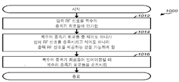
[0085] 도 10은 신호 증폭을 수행하기 위한 프로세스(1000)의 예시적 설계를 도시한다. 프로세스(1000)는 무선 디바이스에 의해 또는 일부 다른 엔티티에 의해 수행될 수 있다. 입력 RF 신호는, 자신들의 입력들이 함께 커플링되게 할 수 있는 복수의 증폭기 회로들에 인가될 수 있다(블록(1012)). 복수의 증폭기 회로들 중 적어도 하나는, 입력 RF 신호를 증폭시키고 적어도 하나의 출력 RF 신호를 제공하도록 인에이블될 수 있다(블록(1014)). 복수의 증폭기 회로들은, 잡음 분할을 수행하고 잡음 피겨를 개선하기 위해, 복수의 증폭기 회로들이 인에이블될 때 적어도 하나의 상호연결 회로를 통해 쇼트될 수 있다(블록(1016)). 각각의 상호연결 회로는 상호연결 회로에 커플링된 2개의 증폭기 회로들의 내부 노드들 또는 출력들을 쇼트시킬 수 있다.[0085] Figure 10 illustrates an exemplary design of a
[0086] 블록(1014)의 예시적 설계에서, 입력 RF 신호는 복수의 증폭기 회로들 내의 복수의 이득 회로들로 증폭될 수 있다. 복수의 증폭기 회로들은 출력 전류들을 제공할 수 있다. 각각의 증폭기 회로로부터의 출력 전류는 복수의 이득 회로들 각각으로부터의 전류의 일부분을 포함할 수 있다.[0086] In an exemplary design of
[0087] 본원에 설명된 잡음 분할(noise splitting)이 있는 증폭기들(예를 들어, SIMO LNA들)은 IC, 아날로그 IC, RFIC, 믹싱된-신호 IC, ASIC, PCB(printed circuit board), 전자 디바이스 등에 구현될 수 있다. 잡음 분할이 있는 증폭기들은 또한, 다양한 IC 프로세스 기술들, 이를테면, CMOS(complementary metal oxide semiconductor), NMOS, PMOS, BJT(bipolar junction transistor), BiCMOS(bipolar-CMOS), SiGe(silicon germanium), GaAs(gallium arsenide), HBT(heterojunction bipolar transistor)들, HEMT(high electron mobility transistor)들, SOI(silicon-on-insulator) 등으로 제조될 수 있다.Amplifiers (eg, SIMO LNAs) with noise splitting as described herein may be used in ICs, analog ICs, RFICs, mixed-signal ICs, ASICs, printed circuit boards Device or the like. Amplifiers with noise division can also be used for various IC process technologies such as complementary metal oxide semiconductor (CMOS), NMOS, PMOS, bipolar junction transistor (BJT), bipolar-CMOS (BiCMOS), silicon germanium (SiGe) gallium arsenide, heterojunction bipolar transistors (HBT), high electron mobility transistors (HEMT), and silicon-on-insulator (SOI).
[0088] 본원에 설명된 잡음 분할이 있는 증폭기를 구현하는 장치는 독립형 디바이스일 수 있거나 또는 더 큰 디바이스의 일부일 수 있다. 디바이스는 (i) 독립형 IC, (ii) 데이터 및/또는 명령들을 저장하기 위한 메모리 IC들을 포함할 수 있는 하나 또는 둘 이상의 IC들의 세트, (iii) RF 수신기(RFR) 또는 RF 송신기/수신기(RTR)와 같은 RFIC, (iv) 이동국 모뎀(MSM)과 같은 ASIC, (v) 다른 디바이스들 내에 내장될 수 있는 모듈, (vi) 수신기, 셀룰러 폰, 무선 디바이스, 핸드셋 또는 모바일 유닛, (vii) 등일 수 있다.[0088] The device implementing the amplifier with noise division described herein may be a stand-alone device or may be part of a larger device. (I) a set of one or more ICs that may include (i) a standalone IC, (ii) memory ICs for storing data and / or instructions, (iii) an RF receiver (RFR) (Iv) an ASIC such as a mobile station modem (MSM), (v) a module that may be embedded in other devices, (vi) a receiver, a cellular phone, a wireless device, a handset or mobile unit, .
[0089] 하나 또는 둘 이상의 예시적 설계들에서, 설명된 기능들은 하드웨어, 소프트웨어, 펌웨어 또는 이들의 임의의 결합으로 구현될 수 있다. 소프트웨어로 구현되는 경우, 기능들은 컴퓨터 판독가능한 매체 상에 하나 또는 둘 이상의 명령들 또는 코드로서 저장되거나 또는 이들을 통해 송신될 수 있다. 컴퓨터 판독가능한 매체는 하나의 장소에서 다른 장소로 컴퓨터 프로그램의 이전을 가능하게 하는 임의의 매체를 포함하는 통신 매체들 및 컴퓨터 저장 매체들 둘 다를 포함한다. 저장 매체들은 컴퓨터에 의해 액세스될 수 있는 임의의 이용가능한 매체들일 수 있다. 제한이 아닌 예로서, 이러한 컴퓨터 판독가능한 매체는 RAM, ROM, EEPROM, CD-ROM 또는 다른 광학 디스크 저장소, 자기 디스크 저장소 또는 다른 자기 저장 디바이스들, 또는 원하는 프로그램 코드를 명령들 또는 데이터 구조들의 형태로 전달 또는 저장하기 위해 이용될 수 있고 컴퓨터에 의해 액세스될 수 있는 임의의 다른 매체를 포함할 수 있다. 또한, 임의의 연결수단이 컴퓨터 판독가능한 매체로 적절히 지칭된다. 예를 들어, 소프트웨어가 동축 케이블, 광섬유 케이블, 트위스티드 페어(twisted pair), 디지털 가입자 회선(DSL), 또는 (적외선, 라디오, 및 마이크로웨이브와 같은) 무선 기술들을 이용하여 웹사이트, 서버, 또는 다른 원격 소스로부터 송신되는 경우, 동축 케이블, 광섬유 케이블, 트위스티드 페어, DSL, 또는 (적외선, 라디오, 및 마이크로웨이브와 같은) 무선 기술들이 매체의 정의 내에 포함된다. 본원에서 이용되는 바와 같은 디스크(disk 및 disc)는 컴팩트 디스크(disc)(CD), 레이저 디스크(disc), 광 디스크(disc), 디지털 다목적 디스크(disc)(DVD), 플로피 디스크(disk) 및 블루-레이 디스크(disc)를 포함하며, 여기서 디스크(disk)들은 통상적으로 데이터를 자기적으로 재생하는 반면, 디스크(disc)들은 레이저들을 이용하여 데이터를 광학적으로 재생한다. 위의 것들의 결합들은 또한 컴퓨터 판독가능한 매체들의 범위 내에 포함되어야 한다.[0089] In one or more exemplary designs, the functions described may be implemented in hardware, software, firmware, or any combination thereof. When implemented in software, the functions may be stored on or transmitted via one or more instructions or code on a computer readable medium. A computer-readable medium includes both communication media and computer storage media including any medium that enables the transfer of a computer program from one place to another. The storage media may be any available media that can be accessed by a computer. By way of example, and not limitation, such computer-readable media can comprise RAM, ROM, EEPROM, CD-ROM or other optical disk storage, magnetic disk storage or other magnetic storage devices, Or any other medium that can be used to transmit or store data and that can be accessed by a computer. Also, any connection means is suitably referred to as a computer-readable medium. For example, if the software is a web site, a server, or a web site using wireless technologies such as coaxial cable, fiber optic cable, twisted pair, digital subscriber line (DSL), or wireless technologies (such as infrared, radio and microwave) When transmitted from a remote source, coaxial cable, fiber optic cable, twisted pair, DSL, or wireless technologies (such as infrared, radio, and microwave) are included within the definition of the medium. Disks and discs as used herein are intended to include CDs, DVDs, DVDs, DVDs, CDs, and DVDs, including compact discs (CD), laser discs, optical discs, digital versatile discs Blu-ray discs, where discs typically reproduce data magnetically, while discs use lasers to optically reproduce data. Combinations of the above should also be included within the scope of computer readable media.
[0090] 본 개시의 이전의 설명은 임의의 당업자가 본 개시를 실시하거나 또는 이용할 수 있도록 제공된다. 본 개시에 대한 다양한 변경들은 당업자들에게 용이하게 명백할 것이고, 본원에서 정의되는 일반적인 원리들은 본 개시의 범위를 벗어나지 않으면서 다른 변형들에 적용될 수 있다. 따라서, 본 개시는 본원에 설명된 예들 및 설계들에 제한되는 것으로 의도된 것이 아니라, 본원에 개시된 원리들 및 신규한 특징들과 일치하는 가장 넓은 범위를 따를 것이다.
[0090] The previous description of the disclosure is provided to enable any person skilled in the art to make or use the disclosure. Various modifications to the disclosure will be readily apparent to those skilled in the art, and the generic principles defined herein may be applied to other variations without departing from the scope of the disclosure. Accordingly, this disclosure is not intended to be limited to the examples and designs described herein, but is to be accorded the widest scope consistent with the principles and novel features disclosed herein.
Claims (20)
입력 RF(radio frequency) 신호를 수신하도록 구성되는 복수의 증폭기 회로들; 및
적어도 하나의 상호연결 회로에 커플링된 상기 복수의 증폭기 회로들 중 적어도 2개를 쇼트(short)시키도록 구성되는 적어도 하나의 상호연결 회로를 포함하는,
장치.As an apparatus,
A plurality of amplifier circuits configured to receive an input radio frequency (RF) signal; And
And at least one interconnecting circuit configured to short-circuit at least two of the plurality of amplifier circuits coupled to the at least one interconnecting circuit.
Device.
상기 복수의 증폭기 회로들은 복수의 이득 회로들 및 복수의 전류 버퍼들을 포함하고,
각각의 증폭기 회로에 대해, 하나의 이득 회로 및 하나의 전류 버퍼를 포함하는,
장치.The method according to claim 1,
The plurality of amplifier circuits including a plurality of gain circuits and a plurality of current buffers,
For each amplifier circuit, one gain circuit and one current buffer,
Device.
각각의 증폭기 회로는 상기 복수의 증폭기 회로들이 입력 RF 신호를 증폭시키고 복수의 출력 RF 신호들을 제공하도록 인에이블될 때, 상기 복수의 이득 회로들 각각으로부터의 전류의 일부분을 포함하는 출력 전류를 제공하도록 구성되는,
장치.3. The method of claim 2,
Wherein each amplifier circuit is configured to provide an output current comprising a portion of the current from each of the plurality of gain circuits when the plurality of amplifier circuits are enabled to amplify an input RF signal and provide a plurality of output RF signals Configured,
Device.
상기 복수의 증폭기 회로들이 인에이블될 때, 상기 적어도 하나의 상호연결 회로는 상기 복수의 증폭기 회로들의 출력들을 쇼트시키도록 구성되는,
장치.The method according to claim 1,
Wherein the at least one interconnecting circuit is configured to short the outputs of the plurality of amplifier circuits when the plurality of amplifier circuits are enabled.
Device.
상기 복수의 증폭기 회로들이 인에이블될 때, 상기 적어도 하나의 상호연결 회로는 상기 복수의 이득 회로들의 출력을 쇼트시키도록 구성되는,
장치.3. The method of claim 2,
Wherein the at least one interconnecting circuit is configured to short the output of the plurality of gain circuits when the plurality of amplifier circuits is enabled.
Device.
상기 적어도 하나의 상호연결 회로는, 상기 복수의 이득 회로들과 상기 복수의 전류 버퍼들 사이에 커플링된 복수의 캐스코드(cascode) 트랜지스터들을 포함하고,
각각의 캐스코드 트랜지스터는, 하나의 증폭기 회로 내의 이득 회로와 또 다른 증폭기 회로 내의 전류 버퍼 사이에 커플링되고,
상기 복수의 증폭기 회로들이 인에이블될 때, 상기 복수의 캐스코드 트랜지스터들은 턴온되는,
장치.3. The method of claim 2,
Wherein the at least one interconnecting circuit comprises a plurality of cascode transistors coupled between the plurality of gain circuits and the plurality of current buffers,
Each cascode transistor is coupled between a gain circuit in one amplifier circuit and a current buffer in another amplifier circuit,
When the plurality of amplifier circuits are enabled, the plurality of cascode transistors are turned on,
Device.
상기 하나의 증폭기 회로가 인에이블되고 상기 복수의 증폭기 회로들 중 나머지 증폭기 회로들이 디스에이블될 때, 상기 복수의 증폭기 회로들 중 하나는 상기 입력 RF 신호를 증폭시키고, 출력 RF 신호를 제공하도록 구성되는,
장치.The method according to claim 1,
When the one amplifier circuit is enabled and the remaining ones of the plurality of amplifier circuits are disabled, one of the plurality of amplifier circuits is configured to amplify the input RF signal and provide an output RF signal ,
Device.
상기 복수의 증폭기 회로들은, 제 1 증폭기 회로 및 제 2 증폭기 회로를 포함하고,
상기 제 1 증폭기 회로는, 제 1 이득 트랜지스터 및 제 1 캐스코드 트랜지스터를 포함하고,
상기 제 2 증폭기 회로는, 제 2 이득 트랜지스터 및 제 2 캐스코드 트랜지스터를 포함하는,
장치.The method according to claim 1,
The plurality of amplifier circuits including a first amplifier circuit and a second amplifier circuit,
The first amplifier circuit comprising a first gain transistor and a first cascode transistor,
Wherein the second amplifier circuit comprises a second gain transistor and a second cascode transistor,
Device.
상기 적어도 하나의 상호연결 회로는, 제 1 캐스코드 트랜지스터 및 제 2 캐스코드 트랜지스터의 드레인들 사이에 커플링된 스위치를 포함하고,
상기 스위치는, 단지 제 1 증폭기 회로 또는 제 2 증폭기 회로가 인에이블될 때 개방되고, 제 1 증폭기 회로 및 제 2 증폭기 회로 둘 모두가 인에이블될 때 폐쇄되는,
장치.9. The method of claim 8,
Wherein the at least one interconnecting circuit comprises a switch coupled between the drains of the first cascode transistor and the second cascode transistor,
The switch is closed when only the first amplifier circuit or the second amplifier circuit is enabled and closed when both the first amplifier circuit and the second amplifier circuit are enabled,
Device.
상기 스위치는,
상기 제 1 캐스코드 트랜지스터의 드레인과 중간 노드 사이에 커플링된 제 1 트랜지스터;
상기 중간 노드와 상기 제 2 캐스코드 트랜지스터의 드레인 사이에 커플링된 제 2 트랜지스터; 및
상기 중간 노드와 회로 접지(ground) 사이에 커플링된 제 3 트랜지스터를 포함하는,
장치.10. The method of claim 9,
Wherein the switch comprises:
A first transistor coupled between a drain and an intermediate node of the first cascode transistor;
A second transistor coupled between the intermediate node and the drain of the second cascode transistor; And
And a third transistor coupled between the intermediate node and a circuit ground.
Device.
상기 스위치는, 제 1 캐스코드 트랜지스터 및 제 2 캐스코드 트랜지스터의 드레인들 사이에 커플링된 트랜지스터를 포함하는,
장치.10. The method of claim 9,
The switch comprising a transistor coupled between the drains of the first cascode transistor and the second cascode transistor,
Device.
상기 적어도 하나의 상호연결 회로는, 제 1 이득 트랜지스터 및 제 2 이득 트랜지스터의 드레인들 사이에 커플링된 캐패시터를 포함하고,
상기 제 1 증폭기 회로가 인에이블될 때, 상기 제 1 캐스코드 트랜지스터는 턴온되고, 상기 제 2 캐스코드 트랜지스터는 턴오프되며,
상기 제 2 증폭기 회로가 인에이블될 때, 상기 제 2 캐스코드 트랜지스터는 턴온되고, 상기 제 1 캐스코드 트랜지스터는 턴오프되며,
상기 제 1 증폭기 회로 및 상기 제 2 증폭기 회로가 인에이블될 때, 제 1 캐스코드 트랜지스터 및 제 2 캐스코드 트랜지스터 둘 모두는 턴온되는,
장치.9. The method of claim 8,
Wherein the at least one interconnecting circuit comprises a first gain transistor and a capacitor coupled between the drains of the second gain transistor,
When the first amplifier circuit is enabled, the first cascode transistor is turned on, the second cascode transistor is turned off,
When the second amplifier circuit is enabled, the second cascode transistor is turned on, the first cascode transistor is turned off,
When the first amplifier circuit and the second amplifier circuit are enabled, both the first cascode transistor and the second cascode transistor are turned on,
Device.
상기 적어도 하나의 상호연결 회로는,
상기 제 1 이득 트랜지스터의 드레인과 상기 제 2 캐스코드 트랜지스터의 드레인 사이에 커플링된 제 3 캐스코드 트랜지스터; 및
상기 제 2 이득 트랜지스터의 드레인과 상기 제 1 캐스코드 트랜지스터의 드레인 사이에 커플링된 제 4 캐스코드 트랜지스터를 포함하고,
상기 제 1 증폭기 회로 및 상기 제 2 증폭기 회로 둘 모두가 인에이블될 때, 상기 제 3 캐스코드 트랜지스터 및 상기 제 4 캐스코드 트랜지스터는 턴온되는,
장치.9. The method of claim 8,
Wherein the at least one interconnecting circuit comprises:
A third cascode transistor coupled between a drain of the first gain transistor and a drain of the second cascode transistor; And
And a fourth cascode transistor coupled between a drain of the second gain transistor and a drain of the first cascode transistor,
Wherein when the first amplifier circuit and the second amplifier circuit are both enabled, the third cascode transistor and the fourth cascode transistor are turned on,
Device.
상기 제 1 증폭기 회로가 인에이블될 때, 단지 상기 제 1 캐스코드 트랜지스터가 턴온되거나, 상기 제 1 캐스코드 트랜지스터 및 제 4 캐스코드 트랜지스터 둘 모두가 턴온되는,
장치.14. The method of claim 13,
When the first amplifier circuit is enabled, only the first cascode transistor is turned on, or both the first cascode transistor and the fourth cascode transistor are turned on,
Device.
상기 제 1 이득 트랜지스터 및 상기 제 2 이득 트랜지스터의 소스들과 회로 접지 사이에 커플링된 인덕터를 더 포함하는,
장치.9. The method of claim 8,
Further comprising an inductor coupled between the sources of the first gain transistor and the second gain transistor and the circuit ground,
Device.
상기 제 1 증폭기 회로에 커플링된 제 1 트랜스포머를 포함하는 제 1 부하 회로; 및
상기 제 2 증폭기 회로에 커플링된 제 2 트랜스포머를 포함하는 제 2 부하 회로를 더 포함하는,
장치.9. The method of claim 8,
A first load circuit including a first transformer coupled to the first amplifier circuit; And
Further comprising a second load circuit comprising a second transformer coupled to the second amplifier circuit,
Device.
입력 RF(radio frequency) 신호를 복수의 증폭기 회로들에 적용시키는 단계;
상기 복수의 증폭기 회로들 중 적어도 하나가 상기 입력 RF 신호를 증폭시키고, 적어도 하나의 출력 RF 신호를 제공하는 것을 가능하게 하는 단계; 및
상기 복수의 증폭기 회로들이 인에이블될 때, 상기 복수의 증폭기 회로들을 쇼트시키는 단계를 포함하는,
방법.As a method,
Applying an input radio frequency (RF) signal to a plurality of amplifier circuits;
Enabling at least one of the plurality of amplifier circuits to amplify the input RF signal and provide at least one output RF signal; And
And shorting the plurality of amplifier circuits when the plurality of amplifier circuits are enabled.
Way.
상기 복수의 증폭기 회로들 내의 복수의 이득 회로들에 의해 상기 입력 RF 신호를 증폭시키는 단계; 및
상기 복수의 증폭기 회로들로부터의 출력 전류들을 제공하는 단계를 더 포함하고,
각각의 증폭기 회로로부터의 출력 전류는, 상기 복수의 이득 회로들 각각으로부터의 전류의 일부분을 포함하는,
방법.18. The method of claim 17,
Amplifying the input RF signal by a plurality of gain circuits in the plurality of amplifier circuits; And
Further comprising providing output currents from the plurality of amplifier circuits,
The output current from each amplifier circuit including a portion of the current from each of the plurality of gain circuits,
Way.
입력 RF(radio frequency) 신호를 수신하도록 구성되는 복수의 증폭 수단; 및
적어도 하나의 상호연결 수단에 커플링된 상기 복수의 증폭 수단 중 적어도 2개를 쇼트시키도록 구성되는 적어도 하나의 상호연결 수단을 포함하는,
장치.
As an apparatus,
A plurality of amplification means configured to receive an input radio frequency (RF) signal; And
At least one interconnecting means configured to short-circuit at least two of said plurality of amplifying means coupled to at least one interconnecting means,
Device.
상기 복수의 증폭 수단은,
상기 입력 RF 신호를 증폭시키도록 구성되는 복수의 이득 수단; 및
상기 복수의 이득 수단에 커플링된 복수의 버퍼 수단을 포함하고,
상기 복수의 증폭 수단이 인에이블될 때, 각각의 증폭 수단은 상기 복수의 이득 수단 각각으로부터의 전류의 일부분을 포함하는 출력 전류를 제공하도록 구성되는,
장치.20. The method of claim 19,
Wherein the plurality of amplifying means comprises:
A plurality of gain means configured to amplify the input RF signal; And
And a plurality of buffer means coupled to the plurality of gain means,
Wherein each amplifying means is configured to provide an output current comprising a portion of the current from each of the plurality of gain means when the plurality of amplifying means is enabled,
Device.
Applications Claiming Priority (3)
| Application Number | Priority Date | Filing Date | Title |
|---|---|---|---|
| US13/656,904 | 2012-10-22 | ||
| US13/656,904 US9543903B2 (en) | 2012-10-22 | 2012-10-22 | Amplifiers with noise splitting |
| PCT/US2013/066230 WO2014066421A1 (en) | 2012-10-22 | 2013-10-22 | Amplifiers with noise splitting |
Related Child Applications (1)
| Application Number | Title | Priority Date | Filing Date |
|---|---|---|---|
| KR1020207017294A Division KR102233361B1 (en) | 2012-10-22 | 2013-10-22 | Amplifiers with noise splitting |
Publications (1)
| Publication Number | Publication Date |
|---|---|
| KR20150077452A true KR20150077452A (en) | 2015-07-07 |
Family
ID=49552421
Family Applications (2)
| Application Number | Title | Priority Date | Filing Date |
|---|---|---|---|
| KR1020157013052A KR20150077452A (en) | 2012-10-22 | 2013-10-22 | Amplifiers with noise splitting |
| KR1020207017294A KR102233361B1 (en) | 2012-10-22 | 2013-10-22 | Amplifiers with noise splitting |
Family Applications After (1)
| Application Number | Title | Priority Date | Filing Date |
|---|---|---|---|
| KR1020207017294A KR102233361B1 (en) | 2012-10-22 | 2013-10-22 | Amplifiers with noise splitting |
Country Status (6)
| Country | Link |
|---|---|
| US (2) | US9543903B2 (en) |
| EP (2) | EP2909929B1 (en) |
| JP (1) | JP6324977B2 (en) |
| KR (2) | KR20150077452A (en) |
| CN (1) | CN104737443B (en) |
| WO (1) | WO2014066421A1 (en) |
Families Citing this family (44)
| Publication number | Priority date | Publication date | Assignee | Title |
|---|---|---|---|---|
| US9026070B2 (en) | 2003-12-18 | 2015-05-05 | Qualcomm Incorporated | Low-power wireless diversity receiver with multiple receive paths |
| US9450665B2 (en) | 2005-10-19 | 2016-09-20 | Qualcomm Incorporated | Diversity receiver for wireless communication |
| US9178669B2 (en) | 2011-05-17 | 2015-11-03 | Qualcomm Incorporated | Non-adjacent carrier aggregation architecture |
| US9252827B2 (en) | 2011-06-27 | 2016-02-02 | Qualcomm Incorporated | Signal splitting carrier aggregation receiver architecture |
| US9154179B2 (en) | 2011-06-29 | 2015-10-06 | Qualcomm Incorporated | Receiver with bypass mode for improved sensitivity |
| US9172402B2 (en) | 2012-03-02 | 2015-10-27 | Qualcomm Incorporated | Multiple-input and multiple-output carrier aggregation receiver reuse architecture |
| US9362958B2 (en) | 2012-03-02 | 2016-06-07 | Qualcomm Incorporated | Single chip signal splitting carrier aggregation receiver architecture |
| US9118439B2 (en) | 2012-04-06 | 2015-08-25 | Qualcomm Incorporated | Receiver for imbalanced carriers |
| US9154356B2 (en) | 2012-05-25 | 2015-10-06 | Qualcomm Incorporated | Low noise amplifiers for carrier aggregation |
| US9867194B2 (en) | 2012-06-12 | 2018-01-09 | Qualcomm Incorporated | Dynamic UE scheduling with shared antenna and carrier aggregation |
| US9300420B2 (en) | 2012-09-11 | 2016-03-29 | Qualcomm Incorporated | Carrier aggregation receiver architecture |
| US9543903B2 (en) * | 2012-10-22 | 2017-01-10 | Qualcomm Incorporated | Amplifiers with noise splitting |
| US9603187B2 (en) | 2012-11-14 | 2017-03-21 | Qualcomm Incorporated | Omni-band amplifiers |
| US8995591B2 (en) | 2013-03-14 | 2015-03-31 | Qualcomm, Incorporated | Reusing a single-chip carrier aggregation receiver to support non-cellular diversity |
| US20140328436A1 (en) * | 2013-05-03 | 2014-11-06 | Nvidia Corporation | Receiver front-end architecture for carrier aggregation |
| US9350310B2 (en) * | 2013-05-24 | 2016-05-24 | Qualcomm Incorporated | Receiver front end for carrier aggregation |
| US9270303B2 (en) | 2013-12-30 | 2016-02-23 | Broadcom Corporation | Configurable receiver architecture for carrier aggregation with multiple-input multiple-output |
| US9413406B2 (en) | 2014-03-14 | 2016-08-09 | Qualcomm Incorporated | Single input multiple-output power amplifier |
| US9774485B2 (en) | 2014-05-16 | 2017-09-26 | Qualcomm Incorporated | Multiplex modules for carrier aggregation receivers |
| US9723560B2 (en) * | 2014-05-22 | 2017-08-01 | Qualcomm Incorporated | Multi-stage amplifier with RC network |
| US9479131B2 (en) | 2014-05-23 | 2016-10-25 | Qualcomm Incorporated | Carrier aggregation amplifier with dual gain control |
| US9642166B2 (en) * | 2014-05-29 | 2017-05-02 | Qualcomm Incorporated | Cross-connected cascode low noise amplifier for carrier aggregation |
| US9379673B2 (en) * | 2014-05-30 | 2016-06-28 | Qualcomm Incorporated | Distortion cancellation for dual stage carrier-aggregation (CA) low noise amplifier (LNA) non-linear second order products |
| US10390343B2 (en) | 2014-06-23 | 2019-08-20 | Qualcomm Incorporated | Carrier aggregation diversity antenna module with integrated LNA banks |
| US9369097B2 (en) * | 2014-09-05 | 2016-06-14 | Qualcomm Incorporated | Multi-band low noise amplifier |
| US9431963B2 (en) | 2014-09-19 | 2016-08-30 | Qualcomm Incorporated | Dual stage low noise amplifier for multiband receiver |
| JP6181731B2 (en) * | 2014-10-31 | 2017-08-16 | スカイワークス ソリューションズ,インコーポレイテッドSkyworks Solutions,Inc. | Diversity receiver front-end system with switching network |
| GB2536089B (en) | 2014-10-31 | 2020-01-08 | Skyworks Solutions Inc | A receiving system |
| DE102015220967B4 (en) * | 2014-10-31 | 2022-08-11 | Skyworks Solutions, Inc. | Diversity receiver in a front-end system with switch network |
| CN105790777B (en) | 2015-01-13 | 2021-02-19 | 三星电子株式会社 | Receiver and wireless terminal for signal processing |
| US9515749B2 (en) | 2015-05-07 | 2016-12-06 | Qualcomm Incorporated | Low noise amplifier module with output coupler |
| DE102015212247A1 (en) * | 2015-06-30 | 2017-01-05 | TRUMPF Hüttinger GmbH + Co. KG | RF amplifier arrangement |
| US9774303B1 (en) * | 2015-08-25 | 2017-09-26 | Marvell International Ltd. | Low-noise amplifier for intra-band non contiguous carrier agregation |
| US10177722B2 (en) | 2016-01-12 | 2019-01-08 | Qualcomm Incorporated | Carrier aggregation low-noise amplifier with tunable integrated power splitter |
| US9800273B1 (en) | 2017-03-01 | 2017-10-24 | Qualcomm Incorporated | Wideband high linearity LNA with intra-band carrier aggregation support |
| US10381991B1 (en) | 2018-02-02 | 2019-08-13 | Psemi Corporation | Drain sharing split LNA |
| TWI643449B (en) * | 2018-04-27 | 2018-12-01 | 立積電子股份有限公司 | Amplifier |
| US10469120B1 (en) | 2018-09-28 | 2019-11-05 | Apple Inc. | Radio frequency front-end circuitry intermediate driver systems and methods |
| JP7185548B2 (en) * | 2019-02-07 | 2022-12-07 | 株式会社東芝 | high frequency amplifier circuit |
| US11025195B2 (en) * | 2019-04-04 | 2021-06-01 | Qualcomm Incorporated | Swing tracking and control |
| US11418156B2 (en) * | 2019-09-22 | 2022-08-16 | Dsp Group Ltd. | Low noise amplifier with improved linearity in low gain mode |
| JP7358316B2 (en) * | 2020-09-17 | 2023-10-10 | 株式会社東芝 | semiconductor circuit |
| US11728838B2 (en) * | 2021-09-21 | 2023-08-15 | Qualcomm Incorporated | Isolating down-conversion mixer for a radio frequency (RF) transceiver |
| US11539382B1 (en) | 2021-10-19 | 2022-12-27 | Psemi Corporation | Supporting wideband inputs on RF receivers |
Family Cites Families (312)
| Publication number | Priority date | Publication date | Assignee | Title |
|---|---|---|---|---|
| US3911364A (en) | 1974-05-09 | 1975-10-07 | Bell Telephone Labor Inc | Cophasing combiner with cochannel signal selector |
| JPS5542790B2 (en) | 1975-01-09 | 1980-11-01 | ||
| US4035729A (en) | 1976-05-21 | 1977-07-12 | General Electric Company | Audio signal quality indicating circuit |
| GB1588367A (en) | 1977-10-18 | 1981-04-23 | Parker B D | Apparatus for selecting one of a plurality of receivers receiving a signal from a single common source |
| US4326294A (en) | 1979-02-13 | 1982-04-20 | Nippon Telegraph & Telephone Public Corporation | Space diversity reception system having compensation means of multipath effect |
| JPS61284125A (en) | 1985-06-11 | 1986-12-15 | Nec Corp | Diversity reception system |
| JPH0683127B2 (en) | 1985-07-22 | 1994-10-19 | 日本電気株式会社 | Diversity receiver radio |
| US4715048A (en) | 1986-05-02 | 1987-12-22 | Canadian Patents And Development Limited | Frequency offset diversity receiving system |
| US4969207A (en) | 1987-03-20 | 1990-11-06 | Nippon Telegraph And Telephone Corporation | Radio receiver with reception deterioration compensation |
| GB8821570D0 (en) | 1988-09-15 | 1989-03-30 | Plessey Co Plc | Course recommendation display |
| JP2638180B2 (en) | 1988-10-26 | 1997-08-06 | 川崎製鉄株式会社 | Low iron loss unidirectional silicon steel sheet and method for producing the same |
| US5390342A (en) | 1990-03-14 | 1995-02-14 | Pioneer Electronic Corporation | Receiver using selective diversity receiving system |
| JP2643614B2 (en) | 1991-02-22 | 1997-08-20 | 日本電気株式会社 | Digital mobile communication terminal |
| US5128630A (en) | 1991-05-03 | 1992-07-07 | Motorola, Inc. | High speed fully differential operational amplifier |
| JPH05102898A (en) | 1991-08-07 | 1993-04-23 | Shiyoudenriyoku Kosoku Tsushin Kenkyusho:Kk | Higher harmonic wave communication system |
| US5321850A (en) | 1991-10-09 | 1994-06-14 | Telefonaktiebolaget L M Ericsson | Diversity radio receiver automatic frequency control |
| JP3301102B2 (en) | 1992-02-14 | 2002-07-15 | ソニー株式会社 | Receiver |
| EP0613260B1 (en) | 1993-02-26 | 2004-09-22 | Kabushiki Kaisha Toshiba | Space diversity receiver for a digital communications system |
| JPH0730452A (en) | 1993-07-12 | 1995-01-31 | Fujitsu Ltd | Receiving circuit |
| US5541963A (en) | 1993-12-01 | 1996-07-30 | Hitachi, Ltd. | Diversity receiving apparatus |
| US5566364A (en) | 1994-01-31 | 1996-10-15 | Nec Corporation | Power saving portable radio communication device with diversity reception |
| JPH07221684A (en) | 1994-02-09 | 1995-08-18 | Hitachi Ltd | Radio terminal equipment of mobile communication |
| JP3022194B2 (en) | 1994-09-02 | 2000-03-15 | 三菱電機株式会社 | Diversity receiver |
| US5694395A (en) | 1994-09-30 | 1997-12-02 | Lucent Technologies, Inc. | Method and apparatus for processing multicarrier signals |
| JP3088246B2 (en) | 1994-10-05 | 2000-09-18 | 三菱電機株式会社 | Wireless communication device |
| GB9424341D0 (en) | 1994-12-02 | 1995-01-18 | Philips Electronics Uk Ltd | Receiver diversity |
| JP3183812B2 (en) | 1995-10-16 | 2001-07-09 | 株式会社エヌ・ティ・ティ・ドコモ | Multiband high frequency circuit for mobile radio |
| US5940452A (en) | 1995-11-29 | 1999-08-17 | Motorola, Inc. | Dual mode radio subscriber unit having a diversity receiver apparatus and method therefor |
| JPH09200070A (en) | 1996-01-12 | 1997-07-31 | Matsushita Electric Ind Co Ltd | Reception circuit |
| DE19630280A1 (en) | 1996-07-26 | 1998-01-29 | Basf Ag | Process for the preparation of cocondensates from aspartic acid and amines |
| US5794159A (en) | 1996-08-07 | 1998-08-11 | Nokia Mobile Phones Limited | Dual band mobile station employing cross-connected transmitter and receiver circuits |
| US6026288A (en) | 1996-12-10 | 2000-02-15 | Lucent Technologies, Inc. | Communications system with an apparatus for controlling overall power consumption based on received signal strength |
| JP3657377B2 (en) | 1996-12-27 | 2005-06-08 | 松下電器産業株式会社 | Receiver circuit |
| FI108486B (en) | 1997-01-31 | 2002-01-31 | Nokia Corp | Method and Circuit Arrangement for Processing Received Signals in a Communication System |
| US6040732A (en) | 1997-04-09 | 2000-03-21 | Analog Devices, Inc. | Switched-transconductance circuit within integrated T-switches |
| JPH11127300A (en) | 1997-10-22 | 1999-05-11 | Canon Inc | Radio communication equipment and its method |
| DE19802373C1 (en) | 1998-01-22 | 1999-06-17 | Siemens Ag | Demodulation circuit for two dimensional data symbols transferred by data communications |
| JP3109504B2 (en) | 1998-03-27 | 2000-11-20 | 日本電気株式会社 | Cellular system, method for avoiding adjacent frequency interference in cellular system, and mobile station |
| US5999990A (en) | 1998-05-18 | 1999-12-07 | Motorola, Inc. | Communicator having reconfigurable resources |
| EP0959567A1 (en) | 1998-05-19 | 1999-11-24 | Robert Bosch Gmbh | Diplexer for mobile phone |
| JP2000013278A (en) | 1998-06-25 | 2000-01-14 | Matsushita Electric Ind Co Ltd | Radio device, radio portable equipment provided with it, radio base station and radio communication system including them |
| US5999815A (en) | 1998-07-08 | 1999-12-07 | Motorola, Inc. | Method and apparatus for implementing diversity for a dual-mode communication unit |
| US6088348A (en) | 1998-07-13 | 2000-07-11 | Qualcom Incorporated | Configurable single and dual VCOs for dual- and tri-band wireless communication systems |
| JP3109595B2 (en) | 1998-08-28 | 2000-11-20 | 日本電気株式会社 | Receive diversity control method and diversity receiver |
| DE19845534B4 (en) | 1998-10-02 | 2005-01-27 | Robert Bosch Gmbh | antenna circuit |
| JP3199039B2 (en) | 1998-11-02 | 2001-08-13 | 日本電気株式会社 | Power consumption reduction circuit, wireless communication device using the same, and power consumption reduction method in wireless communication device |
| DE69920273T2 (en) | 1998-11-12 | 2005-09-22 | Broadcom Corp., Irvine | INTEGRATED TUNER ARCHITECTURE |
| US6430237B1 (en) | 1998-11-16 | 2002-08-06 | Transamerica Business Credit Corporation | Method for accurate signal-to-interference measurement for wireless communication receivers |
| GB2347596B (en) | 1998-12-18 | 2003-07-30 | Mitel Corp | Apparatus for estimating jitter in RTP encapsulated voice packets received over a data network |
| US6522895B1 (en) | 1998-12-31 | 2003-02-18 | Ericsson Inc. | Integrated transmitter and receiver components for a dual-band transceiver |
| US6208844B1 (en) | 1999-02-23 | 2001-03-27 | Conexant Systems, Inc. | System and process for shared functional block communication transceivers with GPS capability |
| JP2000278109A (en) * | 1999-03-19 | 2000-10-06 | Fujitsu Ltd | High frequency switch, changeover type high frequency switch and changeover type high frequency power amplifier |
| US7123891B2 (en) | 1999-06-28 | 2006-10-17 | Skyworks Solutions, Inc. | Wireless communications device allowing a soft handoff procedure in a mobile communications system |
| US6377117B2 (en) | 1999-07-27 | 2002-04-23 | Conexant Systems, Inc. | Method and system for efficiently transmitting energy from an RF device |
| US7260369B2 (en) | 2005-08-03 | 2007-08-21 | Kamilo Feher | Location finder, tracker, communication and remote control system |
| US6684065B2 (en) | 1999-12-20 | 2004-01-27 | Broadcom Corporation | Variable gain amplifier for low voltage applications |
| CN1132344C (en) | 2000-01-04 | 2003-12-24 | 三菱电机株式会社 | Portable telephone set |
| JP2001285114A (en) | 2000-03-28 | 2001-10-12 | Sharp Corp | Plural bands communication equipment sharing antenna |
| AU2001249730A1 (en) | 2000-03-28 | 2001-10-08 | California Institute Of Technology | Concurrent multi-band low noise amplifier architecture |
| JP2002118483A (en) | 2000-10-11 | 2002-04-19 | Matsushita Electric Ind Co Ltd | Radio circuit device and control method thereof |
| US6407689B1 (en) | 2000-11-01 | 2002-06-18 | Qualcomm, Incorporated | Method and apparatus for controlling stages of a multi-stage circuit |
| US6694129B2 (en) | 2001-01-12 | 2004-02-17 | Qualcomm, Incorporated | Direct conversion digital domain control |
| JP2002261880A (en) | 2001-02-28 | 2002-09-13 | Sanyo Electric Co Ltd | Mobile telephone set |
| AU2002231210A1 (en) | 2001-03-14 | 2002-10-03 | California Institute Of Technology | Concurrent dual-band receiver architecture |
| US6424222B1 (en) | 2001-03-29 | 2002-07-23 | Gct Semiconductor, Inc. | Variable gain low noise amplifier for a wireless terminal |
| US6600931B2 (en) | 2001-03-30 | 2003-07-29 | Nokia Corporation | Antenna switch assembly, and associated method, for a radio communication station |
| US6535725B2 (en) | 2001-03-30 | 2003-03-18 | Skyworks Solutions, Inc. | Interference reduction for direct conversion receivers |
| US20020193108A1 (en) | 2001-05-10 | 2002-12-19 | Robinett Robert L. | Multi-mode satellite and terrestrial communication device with position location |
| FI20011217A (en) | 2001-06-08 | 2002-12-09 | Nokia Corp | Reception method, radio system and receiver |
| US7024172B1 (en) | 2001-06-15 | 2006-04-04 | Rockwell Collins, Inc. | Direct conversion receiver using a dithered local oscillator to mitigate adjacent channel coherent interference |
| US6888888B1 (en) | 2001-06-26 | 2005-05-03 | Microsoft Corporation | Simultaneous tuning of multiple channels using intermediate frequency sub-sampling |
| US6985712B2 (en) | 2001-08-27 | 2006-01-10 | Matsushita Electric Industrial Co., Ltd. | RF device and communication apparatus using the same |
| US7061993B2 (en) | 2001-08-29 | 2006-06-13 | Sony Corporation | CDMA receiver architecture for lower bypass switch point |
| US7277679B1 (en) | 2001-09-28 | 2007-10-02 | Arraycomm, Llc | Method and apparatus to provide multiple-mode spatial processing to a terminal unit |
| US6819941B2 (en) | 2001-10-11 | 2004-11-16 | Rf Micro Devices, Inc. | Single output stage power amplification for multimode applications |
| US7116652B2 (en) | 2001-10-18 | 2006-10-03 | Lucent Technologies Inc. | Rate control technique for layered architectures with multiple transmit and receive antennas |
| US20030125040A1 (en) | 2001-11-06 | 2003-07-03 | Walton Jay R. | Multiple-access multiple-input multiple-output (MIMO) communication system |
| US6754510B2 (en) | 2001-12-13 | 2004-06-22 | Superconductor Technologies, Inc. | MEMS-based bypass system for use with a HTS RF receiver |
| US7299021B2 (en) | 2001-12-28 | 2007-11-20 | Nokia Corporation | Method and apparatus for scaling the dynamic range of a receiver for continuously optimizing performance versus power consumption |
| US6816718B2 (en) | 2002-02-07 | 2004-11-09 | Rf Micro Devices, Inc. | DC offset correction using dummy amplifier |
| GB0204108D0 (en) | 2002-02-21 | 2002-04-10 | Analog Devices Inc | 3G radio |
| US6826391B2 (en) | 2002-03-15 | 2004-11-30 | Nokia Corporation | Transmission and reception antenna system for space diversity reception |
| US6728517B2 (en) | 2002-04-22 | 2004-04-27 | Cognio, Inc. | Multiple-input multiple-output radio transceiver |
| CN100340068C (en) | 2002-04-22 | 2007-09-26 | Ipr许可公司 | Multiple-input multiple-output radio transceiver |
| JP4043850B2 (en) | 2002-06-03 | 2008-02-06 | 松下電器産業株式会社 | Diversity switching device |
| JP2004015162A (en) | 2002-06-04 | 2004-01-15 | Hitachi Metals Ltd | Radio frequency circuit for multiband communication system, and antenna switch module |
| US7039377B2 (en) | 2002-06-14 | 2006-05-02 | Skyworks Solutions, Inc. | Switchable gain amplifier |
| US6954446B2 (en) | 2002-06-25 | 2005-10-11 | Motorola, Inc. | Multiple mode RF communication device |
| KR100442833B1 (en) * | 2002-07-12 | 2004-08-02 | 삼성전자주식회사 | Method and apparatus of multi-band RF receiver in mobile unit communication system |
| US6987950B2 (en) | 2002-07-25 | 2006-01-17 | Qualcomm, Incorporated | Radio with duplexer bypass capability |
| US7092737B2 (en) | 2002-07-31 | 2006-08-15 | Mitsubishi Electric Research Laboratories, Inc. | MIMO systems with rate feedback and space time transmit diversity |
| US7212788B2 (en) | 2002-08-13 | 2007-05-01 | Atheros Communications, Inc. | Method and apparatus for signal power loss reduction in RF communication systems |
| US9065537B2 (en) | 2002-09-03 | 2015-06-23 | Broadcom Corporation | Method and system for calibrating a multi-mode, multi-standard transmitter and receiver |
| EP1398887B1 (en) | 2002-09-12 | 2004-11-24 | Siemens Aktiengesellschaft | Dual band diversity receiver |
| JP4189637B2 (en) * | 2002-09-19 | 2008-12-03 | 日本電気株式会社 | FILTER, COMPOSITE FILTER, FILTER MOUNTING BODY WITH THE SAME, INTEGRATED CIRCUIT CHIP, ELECTRONIC DEVICE, AND METHOD FOR CHANGE THE FREQUENCY CHARACTERISTICS OF THE SAME |
| JP3672196B2 (en) | 2002-10-07 | 2005-07-13 | 松下電器産業株式会社 | Antenna device |
| DE10251288B4 (en) | 2002-11-04 | 2005-08-11 | Advanced Micro Devices, Inc., Sunnyvale | Equalizer circuit with notch compensation for a direct mix receiver |
| US6952594B2 (en) | 2002-11-22 | 2005-10-04 | Agilent Technologies, Inc. | Dual-mode RF communication device |
| GB0227626D0 (en) | 2002-11-27 | 2003-01-08 | Koninkl Philips Electronics Nv | Low complexity equalizer for radio receiver |
| US7260377B2 (en) | 2002-12-02 | 2007-08-21 | Broadcom Corporation | Variable-gain low noise amplifier for digital terrestrial applications |
| CN100405739C (en) * | 2002-12-17 | 2008-07-23 | M/A-Com公司 | Series/shunt switch and method of operation |
| US7250804B2 (en) | 2002-12-17 | 2007-07-31 | M/A -Com, Inc. | Series/shunt switch and method of control |
| WO2004057756A1 (en) | 2002-12-19 | 2004-07-08 | Koninklijke Philips Electronics N.V. | Power amplifier with bias control |
| US6806777B2 (en) | 2003-01-02 | 2004-10-19 | Intel Corporation | Ultra wide band low noise amplifier and method |
| US7187735B2 (en) | 2003-01-28 | 2007-03-06 | Raytheon Company | Mixed technology MEMS/SiGe BiCMOS digitalized analog front end with direct RF sampling |
| US7233774B2 (en) * | 2003-01-30 | 2007-06-19 | Broadcom Corporation | RF transceiver with compact stacked mixer design for multiple frequency conversion |
| US7013166B2 (en) | 2003-02-03 | 2006-03-14 | Nokia Corporation | Multi-carrier receiver architecture |
| WO2004073188A1 (en) | 2003-02-07 | 2004-08-26 | Koninklijke Philips Electronics N.V. | Versatile baseband signal input current splitter |
| US7373171B2 (en) | 2003-02-14 | 2008-05-13 | Tdk Corporation | Front end module |
| KR100539781B1 (en) | 2003-02-22 | 2006-01-10 | 엘지전자 주식회사 | A method and a device of setup rf path for dual mode mobile phone |
| JP3999685B2 (en) | 2003-02-26 | 2007-10-31 | 株式会社ケンウッド | Satellite digital radio broadcast receiver |
| DE10311682B3 (en) | 2003-03-11 | 2004-12-02 | Funkwerk Dabendorf-Gmbh | Circuit arrangement for the simultaneous operation of several transmitting and receiving devices on a common antenna |
| US7929985B2 (en) | 2003-05-01 | 2011-04-19 | Telefonaktiebolaget Lm Ericsson (Publ) | Multiple antenna receiver |
| TWI226761B (en) | 2003-05-08 | 2005-01-11 | Ind Tech Res Inst | Dual band transceiver architecture for wireless application |
| TWI225332B (en) | 2003-05-20 | 2004-12-11 | Mediatek Inc | Multi-band low noise amplifier |
| US7929921B2 (en) | 2003-06-10 | 2011-04-19 | Motorola Mobility, Inc. | Diversity control in wireless communications devices and methods |
| US20040266356A1 (en) | 2003-06-27 | 2004-12-30 | Javor Ronald D. | Multiple antenna apparatus and method to provide interference detection and cancellation |
| JP3959374B2 (en) | 2003-06-30 | 2007-08-15 | Tdk株式会社 | USB interface system |
| JP4157506B2 (en) | 2003-07-29 | 2008-10-01 | 株式会社東芝 | Radio receiving apparatus and radio receiving method |
| US7142042B1 (en) | 2003-08-29 | 2006-11-28 | National Semiconductor Corporation | Nulled error amplifier |
| US7403508B1 (en) | 2003-09-22 | 2008-07-22 | Miao George J | Multiband MIMO-based W-CDMA and UWB communications |
| US6917821B2 (en) | 2003-09-23 | 2005-07-12 | Qualcomm, Incorporated | Successive interference cancellation receiver processing with selection diversity |
| US7197291B2 (en) | 2003-10-03 | 2007-03-27 | Motorola, Inc. | Multimode receiver and method for controlling signal interference |
| US7116952B2 (en) | 2003-10-09 | 2006-10-03 | Intel Corporation | Method and apparatus to provide an area efficient antenna diversity receiver |
| US6990357B2 (en) | 2003-10-17 | 2006-01-24 | Nokia Corporation | Front-end arrangements for multiband multimode communication engines |
| US7869528B2 (en) | 2003-10-31 | 2011-01-11 | Northrop Grumman Systems Corporation | Multi-carrier transceiver assembly |
| US20050118977A1 (en) | 2003-12-02 | 2005-06-02 | Drogi Serge F. | Method, apparatus, and systems for digital radio communication systems |
| US9026070B2 (en) | 2003-12-18 | 2015-05-05 | Qualcomm Incorporated | Low-power wireless diversity receiver with multiple receive paths |
| US7649833B2 (en) | 2003-12-29 | 2010-01-19 | Intel Corporation | Multichannel orthogonal frequency division multiplexed receivers with antenna selection and maximum-ratio combining and associated methods |
| US7099646B1 (en) | 2004-01-27 | 2006-08-29 | Marvell International Ltd. | Signal mixer having a single-ended input and a differential output |
| US7444166B2 (en) | 2004-02-12 | 2008-10-28 | Qualcomm Incorporated | Wireless diversity receiver with shared receive path |
| GB0404194D0 (en) | 2004-02-25 | 2004-03-31 | Ttp Communications Ltd | Wireless communication device and method of operating the same |
| US7792151B2 (en) | 2004-02-27 | 2010-09-07 | Nec Corporation | CDMA receiving apparatus and method |
| KR100809795B1 (en) | 2004-03-05 | 2008-03-07 | 콸콤 인코포레이티드 | Multi-antenna receive diversity control in wireless communications |
| US7415260B2 (en) | 2004-03-08 | 2008-08-19 | Standard Microsystems Corporation | Current-mode direct conversion receiver |
| US20070243832A1 (en) | 2004-03-15 | 2007-10-18 | Hyung-Weon Park | Multimode/Multiband Mobile Station and Method for Operating the Same |
| EP1726098A1 (en) | 2004-03-15 | 2006-11-29 | Samsung Electronics Co., Ltd. | Multimode/multiband mobile station and method for operating the same |
| US7493141B2 (en) | 2004-03-15 | 2009-02-17 | Samsung Electronics Co., Ltd. | Common radio architecture for multi-mode multi-band applications |
| US20100253435A1 (en) | 2004-03-18 | 2010-10-07 | Ikuroh Ichitsubo | Rf power amplifier circuit utilizing bondwires in impedance matching |
| US8270927B2 (en) | 2004-03-29 | 2012-09-18 | Qualcom, Incorporated | Adaptive interference filtering |
| US7283851B2 (en) | 2004-04-05 | 2007-10-16 | Qualcomm Incorporated | Power saving mode for receiver circuit blocks based on transmitter activity |
| US7643848B2 (en) | 2004-04-13 | 2010-01-05 | Qualcomm, Incorporated | Multi-antenna transceiver system |
| US7023272B2 (en) | 2004-04-19 | 2006-04-04 | Texas Instruments Incorporated | Multi-band low noise amplifier system |
| DE102004021867B4 (en) | 2004-05-04 | 2012-02-16 | Infineon Technologies Ag | Method for signal processing, in particular in a high-frequency receiver and signal conditioning circuit |
| US7167044B2 (en) | 2004-05-10 | 2007-01-23 | University Of Florida Research Foundation, Inc. | Dual-band CMOS front-end with two gain modes |
| KR100691421B1 (en) | 2004-05-29 | 2007-03-09 | 삼성전자주식회사 | Multi RF splitter and tuner apparatus for Interactive Open-Cable |
| CN1985528B (en) | 2004-06-03 | 2010-06-09 | 高通股份有限公司 | Frequency translating repeater with low cost and high performance local oscillator architecture |
| US7161423B2 (en) | 2004-06-30 | 2007-01-09 | Silicon Laboratories Inc. | Parallel power amplifier and associated methods |
| US7864659B2 (en) | 2004-08-02 | 2011-01-04 | Interdigital Technology Corporation | Quality control scheme for multiple-input multiple-output (MIMO) orthogonal frequency division multiplexing (OFDM) systems |
| US7697905B2 (en) | 2004-09-10 | 2010-04-13 | Qualcomm Incorporation | Local oscillator feedthrough cancellation scheme to remove RF and baseband offsets |
| US7286238B2 (en) | 2004-09-22 | 2007-10-23 | Corning Incorporated | Feature isolation for frequency-shifting interferometry |
| US7787520B2 (en) | 2004-10-06 | 2010-08-31 | Broadcom Corporation | Method and system for channel estimation in a single channel (SC) single-input multiple-output (SIMO) system |
| JP4598831B2 (en) | 2004-11-03 | 2010-12-15 | ワイオニクス リサーチ | Ultra-wideband CMOS transceiver |
| US7764726B2 (en) | 2004-12-01 | 2010-07-27 | Qualomm Incorporated | Systems, methods, and apparatus for jammer rejection |
| US20060121937A1 (en) | 2004-12-07 | 2006-06-08 | Samsung Electronics Co., Ltd. | Wireless transmission/reception apparatus for transmitting/receiving frequency band signals according to mobile communication services |
| JP2006166277A (en) | 2004-12-10 | 2006-06-22 | Hitachi Media Electoronics Co Ltd | Transmission/reception apparatus and module |
| US7466645B2 (en) | 2004-12-21 | 2008-12-16 | Panasonic Corporation | OFDM signal receiving apparatus |
| US7372336B2 (en) | 2004-12-31 | 2008-05-13 | Samsung Electronics Co., Ltd. | Small-sized on-chip CMOS power amplifier having improved efficiency |
| DE602005024441D1 (en) | 2005-01-07 | 2010-12-09 | Fujitsu Ltd | TAG FACILITY, ANTENNA AND PORTABLE CARD |
| TWI277292B (en) | 2005-01-24 | 2007-03-21 | Richwave Technology Corp | Method for transforming output signals of a low-noise amplifier of a wireless transceiver |
| US7333831B2 (en) | 2005-02-07 | 2008-02-19 | Nxp B.V. | Interchangeable receive inputs for band and system swappability in communication systems and related methods |
| JP2006237711A (en) | 2005-02-22 | 2006-09-07 | Renesas Technology Corp | Multi-band low-noise amplifier, multi-band low-noise amplifier module, wireless semiconductor integrated circuit, and multi-band rf module |
| US7787843B2 (en) | 2005-03-29 | 2010-08-31 | Broadcom Corporation | Multiple band direct conversion radio frequency transceiver integrated circuit |
| US7395040B2 (en) | 2005-03-29 | 2008-07-01 | Broadcom Corporation | Multiple band multiple input multiple output transceiver integrated circuit |
| US7356325B2 (en) | 2005-04-04 | 2008-04-08 | Broadcom Corporation | Local oscillation routing plan applicable to a multiple RF band RF MIMO transceiver |
| US7957351B2 (en) | 2005-04-04 | 2011-06-07 | Qualcomm Incorporated | Method and apparatus for management of multi-carrier communications in a wireless communication system |
| US7486941B2 (en) * | 2005-04-04 | 2009-02-03 | Freescale Semiconductor, Inc. | Method and apparatus for dynamic gain and phase compensations |
| US7796956B2 (en) | 2005-05-03 | 2010-09-14 | Telefonaktiebolaget L M Ericsson (Publ) | Receiver for a multi-antenna, multi-band radio |
| US8000302B2 (en) | 2005-06-23 | 2011-08-16 | Qualcomm Incorporated | Adaptive multi-channel modem |
| DE102005035096A1 (en) | 2005-07-27 | 2007-02-01 | Robert Bosch Gmbh | Radio wave receiving device |
| JP4370621B2 (en) | 2005-08-23 | 2009-11-25 | 株式会社カシオ日立モバイルコミュニケーションズ | COMMUNICATION TERMINAL DEVICE, COMMUNICATION CONTROL METHOD, AND COMMUNICATION CONTROL PROGRAM |
| US7751850B2 (en) | 2005-09-01 | 2010-07-06 | Broadcom Corporation | Single chip multimode baseband processing circuitry with a shared radio interface |
| JP4665676B2 (en) | 2005-09-09 | 2011-04-06 | パナソニック株式会社 | Receiver |
| US7483678B2 (en) | 2005-09-27 | 2009-01-27 | Skyworks Solutions, Inc. | Single chip GSM/EDGE transceiver architecture with closed loop power control |
| US9450665B2 (en) | 2005-10-19 | 2016-09-20 | Qualcomm Incorporated | Diversity receiver for wireless communication |
| US7660571B2 (en) | 2005-11-04 | 2010-02-09 | Broadcom Corporation | Programmable attenuator using digitally controlled CMOS switches |
| US7593706B2 (en) | 2005-12-21 | 2009-09-22 | Motorola, Inc. | Dynamic pre-selector for a GPS receiver |
| DE102006004951A1 (en) | 2006-02-01 | 2007-08-09 | Atmel Germany Gmbh | Integrated circuit arrangement for converting a high-frequency bandpass signal into a low-frequency quadrature signal |
| DE102006006291B4 (en) | 2006-02-10 | 2011-07-14 | Infineon Technologies AG, 81669 | Tranceiver arrangement and method for processing a signal |
| US20070197178A1 (en) | 2006-02-21 | 2007-08-23 | Nokia Corporation | Automatic gain control system for receivers in wireless communications |
| US8521198B2 (en) | 2006-05-12 | 2013-08-27 | Qualcomm, Incorporated | Dynamic LNA switch points based on channel conditions |
| JP4640836B2 (en) | 2006-05-30 | 2011-03-02 | 京セラ株式会社 | Wireless communication method and wireless communication apparatus |
| CN101473547A (en) | 2006-06-22 | 2009-07-01 | Nxp股份有限公司 | Dual band receiver with control means for preventing signal overloading |
| US8295371B2 (en) | 2006-07-14 | 2012-10-23 | Qualcomm Incorporated | Multi-carrier receiver for wireless communication |
| JP4864625B2 (en) | 2006-09-28 | 2012-02-01 | 京セラ株式会社 | Wireless communication method and wireless communication apparatus |
| KR100824783B1 (en) | 2006-10-17 | 2008-04-24 | 삼성전자주식회사 | Multi-band Low Noise Amplifier and Multi-band RF Receiver |
| EP1916767B1 (en) | 2006-10-25 | 2010-12-29 | Istituto Superiore Mario Boella | A method and an apparatus for reducing interference frequencies by using a notch filter |
| US8885744B2 (en) | 2006-11-10 | 2014-11-11 | Qualcomm Incorporated | Providing antenna diversity in a wireless communication system |
| GB2443846B (en) | 2006-11-15 | 2011-12-07 | Joseph Timothy Poole | Computing system |
| US7728664B2 (en) | 2006-11-21 | 2010-06-01 | Broadcom Corporation | Low noise amplifier with multiple inputs and multiple outputs |
| US8923780B2 (en) | 2006-12-06 | 2014-12-30 | Broadcom Corporation | Method and system for sharing low noise amplifier circuitry in a single chip bluetooth and wireless local area network |
| US7599675B2 (en) | 2006-12-12 | 2009-10-06 | Telefonaktiebolaget Lm Ericsson (Publ) | Method and apparatus for receiving radio frequency signals |
| WO2008084539A1 (en) | 2007-01-11 | 2008-07-17 | Pioneer Corporation | Radio receiver |
| US8862081B2 (en) | 2007-01-19 | 2014-10-14 | Wi-Lan, Inc. | Transceiver with receive path performance diversity and combiner with jammer detect feedback |
| WO2008092745A1 (en) | 2007-01-30 | 2008-08-07 | Nokia Siemens Networks Gmbh & Co. Kg | A method of communication |
| US8237509B2 (en) * | 2007-02-23 | 2012-08-07 | Qualcomm, Incorporated | Amplifier with integrated filter |
| CN101617469A (en) * | 2007-02-23 | 2009-12-30 | 高通股份有限公司 | Amplifier with integrated filter |
| US7719352B2 (en) | 2007-03-13 | 2010-05-18 | Qualcomm Incorporated | Active circuits with isolation switches |
| US7764932B2 (en) | 2007-03-14 | 2010-07-27 | Broadcom Corporation | Antenna system for use within a wireless communication device |
| US7978024B2 (en) | 2007-03-15 | 2011-07-12 | Marvell International Ltd. | Integrated balanced-unbalanced duplexer |
| US7586458B2 (en) | 2007-03-19 | 2009-09-08 | Ahmadreza Rofougaran | Method and system for using a transformer for FM transmit and FM receive functionality |
| US7952398B2 (en) | 2007-04-27 | 2011-05-31 | Avago Technologies Enterprise IP (Singapore) Pte. Ltd. | Bias circuit for common-mode and semiconductor process voltage and temperature optimization for a receiver assembly |
| US8090369B2 (en) | 2007-05-01 | 2012-01-03 | Qualcomm Incorporated | User equipment capability handling in long-term evolution systems |
| EP1993201A1 (en) | 2007-05-18 | 2008-11-19 | Interuniversitair Microelektronica Centrum Vzw | Switchable multiband LNA design |
| US7486135B2 (en) | 2007-05-29 | 2009-02-03 | Telefonaktiebolaget Lm Ericsson (Publ) | Configurable, variable gain LNA for multi-band RF receiver |
| JP5566570B2 (en) | 2007-05-30 | 2014-08-06 | 京セラ株式会社 | Wireless communication terminal |
| JP4416014B2 (en) * | 2007-06-26 | 2010-02-17 | ソニー株式会社 | Wireless communication device |
| US7570111B1 (en) | 2007-06-28 | 2009-08-04 | Rockwell Collins, Inc. | Apparatus and method for wideband amplification of RF signals |
| JP2009027778A (en) | 2007-07-17 | 2009-02-05 | Toyota Motor Corp | Bus bar |
| GB0717042D0 (en) | 2007-09-03 | 2007-10-10 | Toumaz Technology Ltd | Multiplier, mixer, modulator, receiver and transmitter |
| US8290449B2 (en) | 2007-09-18 | 2012-10-16 | California Institute Of Technology | Equalization of third-order intermodulation products in wideband direct conversion receiver |
| US8139670B1 (en) | 2007-09-21 | 2012-03-20 | Marvell International Ltd. | Modular MIMO transceiver architecture |
| JP2009124189A (en) | 2007-11-09 | 2009-06-04 | Nsc Co Ltd | Automatic gain control circuit |
| JP2009130867A (en) | 2007-11-28 | 2009-06-11 | Renesas Technology Corp | Semiconductor integrated circuit |
| US8090332B2 (en) | 2007-12-12 | 2012-01-03 | Qualcomm, Incorporated | Tracking filter for a receiver |
| US7944298B2 (en) | 2007-12-18 | 2011-05-17 | Qualcomm, Incorporated | Low noise and low input capacitance differential MDS LNA |
| US8295778B2 (en) | 2008-01-11 | 2012-10-23 | Apple Inc. | Channel rank feedback in multiple-input multiple-output communication systems |
| CN101242158B (en) | 2008-03-07 | 2010-08-04 | 武汉芯泰科技有限公司 | A configurable and reconstructable dynamic frequency mixer |
| US7656230B2 (en) | 2008-03-21 | 2010-02-02 | Qualcomm, Incorporated | Quadrature output low noise transconductance amplifier having differential input |
| EP2265899B1 (en) | 2008-04-01 | 2018-10-03 | Sensus Spectrum LLC | Universal software defined home gateway |
| US8345798B2 (en) | 2008-05-21 | 2013-01-01 | Entropic Communications, Inc. | Channel stacking system and method of operation |
| KR101714507B1 (en) | 2008-05-22 | 2017-03-09 | 삼성전자주식회사 | Receive circuit and method for operating balun circuit and notch filter |
| US8238410B2 (en) | 2008-06-27 | 2012-08-07 | Csr Technology Inc. | Method and apparatus for mitigating the effects of narrowband interfering signals in a GPS receiver |
| US8149955B2 (en) | 2008-06-30 | 2012-04-03 | Telefonaktiebolaget L M Ericsson (Publ) | Single ended multiband feedback linearized RF amplifier and mixer with DC-offset and IM2 suppression feedback loop |
| EP2141818B1 (en) | 2008-07-04 | 2011-12-28 | TELEFONAKTIEBOLAGET LM ERICSSON (publ) | Signal processing device and method |
| US8055229B2 (en) | 2008-07-22 | 2011-11-08 | Maxrise Inc. | Low noise, highly linear amplifying stage and signal receiver using the same |
| US20100019967A1 (en) | 2008-07-25 | 2010-01-28 | Farrokh Farrokhi | Method and apparatus for determining location |
| US8588151B2 (en) | 2008-08-08 | 2013-11-19 | Qualcomm Incorporated | Access terminal capability update |
| US8306494B2 (en) | 2008-08-14 | 2012-11-06 | Broadcom Corporation | Method and system for a single-ended input low noise amplifier with differential output |
| US8571510B2 (en) | 2008-08-18 | 2013-10-29 | Qualcomm Incorporated | High linearity low noise receiver with load switching |
| US8249538B2 (en) | 2008-11-24 | 2012-08-21 | Cisco Technology, Inc. | Offset direct conversion receiver |
| US8494470B2 (en) * | 2008-11-25 | 2013-07-23 | Silicon Laboratories Inc. | Integrated receivers and integrated circuit having integrated inductors |
| US8242841B2 (en) | 2008-12-05 | 2012-08-14 | Csr Technology Inc. | Receiver having multi-stage low noise amplifier |
| US8514015B2 (en) | 2008-12-10 | 2013-08-20 | Qualcomm, Incorporated | Amplifier with programmable off voltage |
| US7911269B2 (en) | 2009-01-19 | 2011-03-22 | Qualcomm Incorporated | Ultra low noise high linearity LNA for multi-mode transceiver |
| US20100197263A1 (en) | 2009-01-30 | 2010-08-05 | Research In Motion Limited | Method and apparatus for combined multi-carrier reception and receive antenna diversity |
| US8755476B2 (en) | 2009-02-01 | 2014-06-17 | Qualcomm Incorporated | Apparatus and method for antenna switching diversity in an OFDM system |
| US8583170B2 (en) | 2009-02-16 | 2013-11-12 | Telefonaktiebolaget Lm Ericsson (Publ) | Multi-band aggregated spectrum receiver employing frequency source reuse |
| US8073401B2 (en) | 2009-02-17 | 2011-12-06 | Rfaxis, Inc. | Multi mode radio frequency transceiver front end circuit with inter-stage matching circuit |
| US20100214184A1 (en) | 2009-02-24 | 2010-08-26 | Qualcomm Incorporated | Antenna devices and systems for multi-band coverage in a compact volume |
| US9231680B2 (en) | 2009-03-03 | 2016-01-05 | Rfaxis, Inc. | Multi-channel radio frequency front end circuit |
| US8305986B2 (en) | 2009-03-09 | 2012-11-06 | Samsung Electronics Co., Ltd. | Method and apparatus for uplink transmissions and CQI reports with carrier aggregation |
| US8233524B2 (en) | 2009-03-12 | 2012-07-31 | Freescale Semiconductor, Inc. | Radio transmitter IQ imbalance measurement and correction methods and apparatus |
| US8022772B2 (en) | 2009-03-19 | 2011-09-20 | Qualcomm Incorporated | Cascode amplifier with protection circuitry |
| US8031005B2 (en) | 2009-03-23 | 2011-10-04 | Qualcomm, Incorporated | Amplifier supporting multiple gain modes |
| US8576768B2 (en) | 2009-04-16 | 2013-11-05 | Qualcomm Incorporated | Hybrid multi-band receiver |
| US7786807B1 (en) | 2009-04-23 | 2010-08-31 | Broadcom Corporation | Cascode CMOS RF power amplifier with programmable feedback cascode bias under multiple supply voltages |
| CN101873148B (en) | 2009-04-23 | 2013-09-18 | 鸿富锦精密工业(深圳)有限公司 | Radio frequency module and wireless communication device using same |
| TWI407738B (en) | 2009-04-24 | 2013-09-01 | Mediatek Inc | Carrier assignment method and base station |
| US8848771B2 (en) | 2009-05-14 | 2014-09-30 | Qualcomm Incorporated | System and method for simultaneous operation of multiple modems using a single transceiver |
| US8270499B2 (en) | 2009-05-15 | 2012-09-18 | Qualcomm, Incorporated | Receiver with balanced I/Q transformer |
| US8175566B2 (en) | 2009-06-04 | 2012-05-08 | Qualcomm, Incorporated | Multiple multi-mode low-noise amplifier receiver with shared degenerative inductors |
| US8130145B2 (en) | 2009-06-24 | 2012-03-06 | Qualcomm Incorporated | Receive diversity in GNSS receivers |
| US8824967B2 (en) | 2009-06-26 | 2014-09-02 | Qualcomm Incorporated | Dynamically changing a transmitter sampling frequency for a digital-to-analog converter (DAC) to reduce interference from DAC images |
| US9185718B2 (en) | 2009-06-29 | 2015-11-10 | Qualcomm Incorporated | Centralized coexistence manager for controlling operation of multiple radios |
| JP2011015112A (en) | 2009-07-01 | 2011-01-20 | Hitachi Kokusai Electric Inc | Radio receiver |
| US8102213B2 (en) | 2009-07-23 | 2012-01-24 | Qualcomm, Incorporated | Multi-mode low noise amplifier with transformer source degeneration |
| US8310312B2 (en) | 2009-08-11 | 2012-11-13 | Qualcomm, Incorporated | Amplifiers with improved linearity and noise performance |
| US20110194504A1 (en) | 2009-08-12 | 2011-08-11 | Qualcomm Incorporated | Method and apparatus for supporting single-user multiple-input multiple-output (su-mimo) and multi-user mimo (mu-mimo) |
| GB2472978A (en) | 2009-08-24 | 2011-03-02 | Vodafone Plc | A multi-antenna receiver is switched between receiver diversity mode and carrier aggregation mode on the basis of network or/and terminal parameters |
| US8638682B2 (en) | 2009-10-01 | 2014-01-28 | Qualcomm Incorporated | Method and apparatus for conducting measurements when multiple carriers are supported |
| JP2011082669A (en) | 2009-10-05 | 2011-04-21 | Mitsubishi Electric Corp | Digital broadcast receiver |
| US9059773B2 (en) | 2009-10-11 | 2015-06-16 | SiTune Corporation | Radio frequency tuner |
| JP4740365B2 (en) | 2009-10-26 | 2011-08-03 | シャープ株式会社 | Mobile station apparatus, base station apparatus, radio communication system, communication control method, communication control program, and processor |
| CN102056296B (en) | 2009-10-30 | 2016-03-30 | 索尼株式会社 | Resource allocation methods in communication network and device |
| US8217723B2 (en) | 2009-11-05 | 2012-07-10 | Texas Instruments Incorporated | Low noise amplifier circuit |
| JP2011119807A (en) | 2009-12-01 | 2011-06-16 | Mitsubishi Electric Corp | Radio apparatus and radio communication method of the same |
| JP5355366B2 (en) | 2009-12-02 | 2013-11-27 | 株式会社東芝 | Differential amplifier circuit and radio receiver |
| JP5446823B2 (en) | 2009-12-16 | 2014-03-19 | ソニー株式会社 | Method for handover, terminal device, base station, and radio communication system |
| US20110250926A1 (en) | 2009-12-21 | 2011-10-13 | Qualcomm Incorporated | Dynamic antenna selection in a wireless device |
| WO2011085125A1 (en) | 2010-01-06 | 2011-07-14 | Rfaxis, Inc. | Transmit-receive radio frequency front end integrated circuits for laptop computer applications |
| EP2348642B8 (en) | 2010-01-26 | 2017-04-05 | OCT Circuit Technologies International Limited | Process for achieving spur mitigation in an integrated circuit including a wide band receiver |
| WO2011094284A1 (en) | 2010-01-26 | 2011-08-04 | Maxlinear, Inc. | Diversity receiver |
| US8725097B2 (en) | 2010-02-09 | 2014-05-13 | Broadcom Corporation | Amplifier for cable and terrestrial applications with independent stage frequency tilt |
| CN101789805B (en) * | 2010-02-24 | 2014-03-12 | 华为技术有限公司 | Amplifying device and signal processing method based on same |
| CN102844983B (en) | 2010-03-02 | 2015-07-15 | 马维尔国际贸易有限公司 | Dual carrier amplifier circuits and methods |
| US8537723B2 (en) | 2010-03-12 | 2013-09-17 | Rf Micro Devices, Inc. | LTE-Advanced (4G) front end radio architecture |
| US8483156B2 (en) | 2010-05-03 | 2013-07-09 | Nokia Siemens Networks Oy | Feedback for inter-radio access technology carrier aggregation |
| US8565352B2 (en) | 2010-05-03 | 2013-10-22 | Telefonaktiebolaget L M Ericsson (Publ) | Digital IQ imbalance compensation for dual-carrier double conversion receiver |
| US8626084B2 (en) * | 2010-05-13 | 2014-01-07 | Qualcomm, Incorporated | Area efficient concurrent matching transceiver |
| US9083393B2 (en) | 2010-06-01 | 2015-07-14 | Lg Electronics Inc. | User equipment for simultaneously transmitting signals to which different wireless communication systems are applied through a plurality of frequency bands |
| US9031515B2 (en) | 2010-06-03 | 2015-05-12 | Broadcom Corporation | Transceiver including a weaved connection |
| US8842582B2 (en) | 2010-06-04 | 2014-09-23 | Qualcomm Incorporated | Reducing power consumption by taking advantage of superior in-circuit duplexer performance |
| EP2398285B1 (en) | 2010-06-18 | 2016-11-16 | Alcatel Lucent | Power saving |
| US8670726B2 (en) | 2010-07-08 | 2014-03-11 | Microsemi Corporation | Architecture for coexistence of multiple band radios |
| US8493126B2 (en) | 2010-07-15 | 2013-07-23 | Qualcomm Incorporated | Wideband balun having a single primary and multiple secondaries |
| US9036583B2 (en) | 2010-07-16 | 2015-05-19 | Lg Electronics Inc. | Transmission method and apparatus for carrier aggregation and uplink MIMO |
| US8437299B2 (en) | 2010-08-17 | 2013-05-07 | Qualcomm Incorporated | Radio channel aggregation and segmentation |
| US8310314B2 (en) | 2010-09-06 | 2012-11-13 | Mediatek Inc. | Signal amplification circuits for receiving/transmitting signals according to input signal |
| WO2012049529A1 (en) | 2010-10-15 | 2012-04-19 | Freescale Semiconductor, Inc. | Integrated circuit device, wireless communication unit and method of manufacture therefor |
| US8837331B2 (en) | 2011-02-02 | 2014-09-16 | Qualcomm Incorporated | Duplexer bypass |
| US9178669B2 (en) | 2011-05-17 | 2015-11-03 | Qualcomm Incorporated | Non-adjacent carrier aggregation architecture |
| US8514021B2 (en) | 2011-05-19 | 2013-08-20 | Renesas Mobile Corporation | Radio frequency integrated circuit |
| US9252827B2 (en) | 2011-06-27 | 2016-02-02 | Qualcomm Incorporated | Signal splitting carrier aggregation receiver architecture |
| US20120329395A1 (en) | 2011-06-27 | 2012-12-27 | Qualcomm Atheros, Inc. | Dynamic antenna sharing |
| US9882602B2 (en) | 2011-06-29 | 2018-01-30 | Qualcomm Incorporated | Global navigation satellite system receiver with filter bypass mode for improved sensitivity |
| US9154179B2 (en) | 2011-06-29 | 2015-10-06 | Qualcomm Incorporated | Receiver with bypass mode for improved sensitivity |
| US20130043946A1 (en) * | 2011-08-16 | 2013-02-21 | Qualcomm Incorporated | Low noise amplifiers with combined outputs |
| US8892057B2 (en) | 2011-08-23 | 2014-11-18 | Rf Micro Devices, Inc. | Carrier aggregation radio system |
| WO2013036794A1 (en) | 2011-09-08 | 2013-03-14 | Drexel University | Reconfigurable antenna based solutions for device authentication and instrusion detection in wireless networks |
| US8774334B2 (en) | 2011-11-09 | 2014-07-08 | Qualcomm Incorporated | Dynamic receiver switching |
| GB201119888D0 (en) | 2011-11-17 | 2011-12-28 | Renesas Mobile Corp | Methods of receiving and receivers |
| EP2615764A3 (en) | 2011-11-30 | 2014-04-09 | Sequans Communications Limited | Carrier aggregation aparatus |
| US9172402B2 (en) | 2012-03-02 | 2015-10-27 | Qualcomm Incorporated | Multiple-input and multiple-output carrier aggregation receiver reuse architecture |
| US9362958B2 (en) | 2012-03-02 | 2016-06-07 | Qualcomm Incorporated | Single chip signal splitting carrier aggregation receiver architecture |
| US9118439B2 (en) | 2012-04-06 | 2015-08-25 | Qualcomm Incorporated | Receiver for imbalanced carriers |
| US9154356B2 (en) | 2012-05-25 | 2015-10-06 | Qualcomm Incorporated | Low noise amplifiers for carrier aggregation |
| US9867194B2 (en) | 2012-06-12 | 2018-01-09 | Qualcomm Incorporated | Dynamic UE scheduling with shared antenna and carrier aggregation |
| US8909186B2 (en) * | 2012-07-16 | 2014-12-09 | Intel Mobile Communications GmbH | Receiver, method and mobile communication device |
| US9300420B2 (en) | 2012-09-11 | 2016-03-29 | Qualcomm Incorporated | Carrier aggregation receiver architecture |
| US9543903B2 (en) * | 2012-10-22 | 2017-01-10 | Qualcomm Incorporated | Amplifiers with noise splitting |
| US8995591B2 (en) | 2013-03-14 | 2015-03-31 | Qualcomm, Incorporated | Reusing a single-chip carrier aggregation receiver to support non-cellular diversity |
-
2012
- 2012-10-22 US US13/656,904 patent/US9543903B2/en active Active
-
2013
- 2013-10-22 EP EP13788822.8A patent/EP2909929B1/en active Active
- 2013-10-22 KR KR1020157013052A patent/KR20150077452A/en active Application Filing
- 2013-10-22 JP JP2015538143A patent/JP6324977B2/en active Active
- 2013-10-22 EP EP20186946.8A patent/EP3790190B1/en active Active
- 2013-10-22 KR KR1020207017294A patent/KR102233361B1/en active IP Right Grant
- 2013-10-22 WO PCT/US2013/066230 patent/WO2014066421A1/en active Application Filing
- 2013-10-22 CN CN201380054734.1A patent/CN104737443B/en active Active
-
2016
- 2016-12-12 US US15/375,502 patent/US9837968B2/en active Active
Also Published As
| Publication number | Publication date |
|---|---|
| CN104737443B (en) | 2018-06-01 |
| JP6324977B2 (en) | 2018-05-16 |
| CN104737443A (en) | 2015-06-24 |
| JP2015532567A (en) | 2015-11-09 |
| US9837968B2 (en) | 2017-12-05 |
| US20140113578A1 (en) | 2014-04-24 |
| EP2909929B1 (en) | 2020-07-22 |
| US20170093343A1 (en) | 2017-03-30 |
| EP3790190B1 (en) | 2023-03-01 |
| WO2014066421A1 (en) | 2014-05-01 |
| EP3790190A1 (en) | 2021-03-10 |
| KR20200074264A (en) | 2020-06-24 |
| KR102233361B1 (en) | 2021-03-26 |
| US9543903B2 (en) | 2017-01-10 |
| EP2909929A1 (en) | 2015-08-26 |
Similar Documents
| Publication | Publication Date | Title |
|---|---|---|
| KR102233361B1 (en) | Amplifiers with noise splitting | |
| US9059665B2 (en) | Amplifiers with multiple outputs and configurable degeneration inductor | |
| US9154357B2 (en) | Multiple-input multiple-output (MIMO) low noise amplifiers for carrier aggregation | |
| US9548709B2 (en) | Independent gain control for multiple receive circuits concurrently processing different transmitted signals | |
| US20130043946A1 (en) | Low noise amplifiers with combined outputs | |
| US9048928B2 (en) | Expandable transceivers and receivers |
Legal Events
| Date | Code | Title | Description |
|---|---|---|---|
| A201 | Request for examination | ||
| E902 | Notification of reason for refusal | ||
| E701 | Decision to grant or registration of patent right | ||
| A107 | Divisional application of patent |