KR20150017543A - Ultraviolet Light Emitting Device - Google Patents
Ultraviolet Light Emitting Device Download PDFInfo
- Publication number
- KR20150017543A KR20150017543A KR1020130093616A KR20130093616A KR20150017543A KR 20150017543 A KR20150017543 A KR 20150017543A KR 1020130093616 A KR1020130093616 A KR 1020130093616A KR 20130093616 A KR20130093616 A KR 20130093616A KR 20150017543 A KR20150017543 A KR 20150017543A
- Authority
- KR
- South Korea
- Prior art keywords
- layer
- semiconductor layer
- conductive type
- light emitting
- electrode
- Prior art date
Links
Images


Classifications
-
- H—ELECTRICITY
- H01—ELECTRIC ELEMENTS
- H01L—SEMICONDUCTOR DEVICES NOT COVERED BY CLASS H10
- H01L33/00—Semiconductor devices with at least one potential-jump barrier or surface barrier specially adapted for light emission; Processes or apparatus specially adapted for the manufacture or treatment thereof or of parts thereof; Details thereof
- H01L33/02—Semiconductor devices with at least one potential-jump barrier or surface barrier specially adapted for light emission; Processes or apparatus specially adapted for the manufacture or treatment thereof or of parts thereof; Details thereof characterised by the semiconductor bodies
- H01L33/10—Semiconductor devices with at least one potential-jump barrier or surface barrier specially adapted for light emission; Processes or apparatus specially adapted for the manufacture or treatment thereof or of parts thereof; Details thereof characterised by the semiconductor bodies with a light reflecting structure, e.g. semiconductor Bragg reflector
-
- H—ELECTRICITY
- H01—ELECTRIC ELEMENTS
- H01L—SEMICONDUCTOR DEVICES NOT COVERED BY CLASS H10
- H01L33/00—Semiconductor devices with at least one potential-jump barrier or surface barrier specially adapted for light emission; Processes or apparatus specially adapted for the manufacture or treatment thereof or of parts thereof; Details thereof
- H01L33/02—Semiconductor devices with at least one potential-jump barrier or surface barrier specially adapted for light emission; Processes or apparatus specially adapted for the manufacture or treatment thereof or of parts thereof; Details thereof characterised by the semiconductor bodies
- H01L33/20—Semiconductor devices with at least one potential-jump barrier or surface barrier specially adapted for light emission; Processes or apparatus specially adapted for the manufacture or treatment thereof or of parts thereof; Details thereof characterised by the semiconductor bodies with a particular shape, e.g. curved or truncated substrate
- H01L33/22—Roughened surfaces, e.g. at the interface between epitaxial layers
-
- H—ELECTRICITY
- H01—ELECTRIC ELEMENTS
- H01L—SEMICONDUCTOR DEVICES NOT COVERED BY CLASS H10
- H01L33/00—Semiconductor devices with at least one potential-jump barrier or surface barrier specially adapted for light emission; Processes or apparatus specially adapted for the manufacture or treatment thereof or of parts thereof; Details thereof
- H01L33/36—Semiconductor devices with at least one potential-jump barrier or surface barrier specially adapted for light emission; Processes or apparatus specially adapted for the manufacture or treatment thereof or of parts thereof; Details thereof characterised by the electrodes
- H01L33/38—Semiconductor devices with at least one potential-jump barrier or surface barrier specially adapted for light emission; Processes or apparatus specially adapted for the manufacture or treatment thereof or of parts thereof; Details thereof characterised by the electrodes with a particular shape
-
- H—ELECTRICITY
- H01—ELECTRIC ELEMENTS
- H01L—SEMICONDUCTOR DEVICES NOT COVERED BY CLASS H10
- H01L33/00—Semiconductor devices with at least one potential-jump barrier or surface barrier specially adapted for light emission; Processes or apparatus specially adapted for the manufacture or treatment thereof or of parts thereof; Details thereof
- H01L33/36—Semiconductor devices with at least one potential-jump barrier or surface barrier specially adapted for light emission; Processes or apparatus specially adapted for the manufacture or treatment thereof or of parts thereof; Details thereof characterised by the electrodes
- H01L33/40—Materials therefor
- H01L33/405—Reflective materials
-
- H—ELECTRICITY
- H01—ELECTRIC ELEMENTS
- H01L—SEMICONDUCTOR DEVICES NOT COVERED BY CLASS H10
- H01L33/00—Semiconductor devices with at least one potential-jump barrier or surface barrier specially adapted for light emission; Processes or apparatus specially adapted for the manufacture or treatment thereof or of parts thereof; Details thereof
- H01L33/36—Semiconductor devices with at least one potential-jump barrier or surface barrier specially adapted for light emission; Processes or apparatus specially adapted for the manufacture or treatment thereof or of parts thereof; Details thereof characterised by the electrodes
- H01L33/40—Materials therefor
- H01L33/42—Transparent materials
Abstract
Description
실시 예는 자외선 발광 소자에 관한 것이다.An embodiment relates to an ultraviolet light emitting element.
발광 다이오드(LED:Light Emitting Diode)는 화합물 반도체의 특성을 이용하여 전기를 적외선 또는 빛으로 변환시켜서 신호를 주고 받거나, 광원으로 사용되는 반도체 소자의 일종이다.Light emitting diodes (LEDs) are a kind of semiconductor devices that convert the electricity into infrared rays or light by using the characteristics of compound semiconductors, exchange signals, or use as a light source.
Ⅲ-Ⅴ족 질화물 반도체(group Ⅲ-Ⅴ nitride semiconductor)는 물리적 및 화학적 특성으로 인해 발광 다이오드(LED) 또는 레이저 다이오드(LD:Laser Diode) 등 발광소자의 핵심 소재로 각광을 받고 있다.III-V nitride semiconductors (group III-V nitride semiconductors) are attracting attention as a core material for light emitting devices such as light emitting diodes (LEDs) and laser diodes (LDs) due to their physical and chemical properties.
이러한 발광 다이오드는 백열등과 형광등 등의 기존 조명기구에 사용되는 수은(Hg)과 같은 환경 유해물질이 포함되어 있지 않아 우수한 친환경성을 가지며, 긴 수명과 저전력 소비특성 등과 같은 장점이 있기 때문에 기존의 광원들을 대체하고 있다.Since such a light emitting diode does not contain environmentally harmful substances such as mercury (Hg) used in conventional lighting devices such as incandescent lamps and fluorescent lamps, it has excellent environmental friendliness, and has advantages such as long life and low power consumption characteristics. .
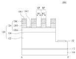
도 1은 기존의 발광 소자의 단면도로서, 기판(10), 발광 구조물(20), n형 전극(32) 및 p형 전극(34)으로 구성된다.1 is a cross-sectional view of a conventional light emitting device, which is composed of a
도 1의 기판(10) 위에 배치된 발광 구조물(20)은 n형 반도체층(22), 활성층(24) 및 p형 반도체층(26)으로 구성된다. 그리고, n형 전극(32)은 n형 반도체층(22) 위에 배치되고, p형 전극(34)은 p형 반도체층(26) 위에 배치된다.The
만일, 활성층(24)에서 자외선 파장 대역의 광이 방출되고 n형 및 p형 반도체층(22, 26) 각각이 GaN으로 이루어져 있다면, 광은 n형 및 p형 GaN층(22, 26)에서 흡수되어 광 추출 효율이 악화될 수 있다. 이를 개선하기 위해, n형 및 p형 반도체층(22, 26) 각각을 AlGaN으로 형성할 경우 광량은 개선되지만 p형 AlGaN층(26A)을 통해 정공의 주입이 수월하지 않을 수 있다. 이를 해소하기 위해, p형 AlGaN층(26A) 위에 p형 GaN층(26B)을 더 배치할 수 있다. 그러나, p형 GaN층(26B)에서 광이 흡수되므로 광 추출 효율이 낮아짐은 불가피하다.If light in the ultraviolet wavelength band is emitted from the
실시 예는 광 추출 효율을 개선한 자외선 발광 소자를 제공한다.The embodiment provides an ultraviolet light-emitting device improved in light extraction efficiency.
실시 예의 자외선 발광 소자는 제1 도전형 반도체층; 상기 제1 도전형 반도체층 위에 배치되며, 자외선 파장 대역의 광을 방출하는 활성층; 상기 활성층 위에 배치된 제2 도전형 제1 반도체층; 상기 제2 도전형 제1 반도체층 위에 배치되며, 상기 활성층으로부터 방출된 광이 입사되는 방향에 따른 다른 반사율로 상기 광을 반사시키는 제2 도전형 반사층; 및 상기 제2 도전형 반사층 위에 배치되는 제2 도전형 제2 반도체층을 포함하고, 상기 제2 도전형 반사층과 상기 제2 도전형 제2 반도체층은 요철부를 포함하고, 상기 요부는 상기 제2 도전형 제1 반도체층을 노출시킨다.The ultraviolet light-emitting element of the embodiment includes a first conductivity type semiconductor layer; An active layer disposed on the first conductive semiconductor layer and emitting light in an ultraviolet wavelength band; A second conductive type first semiconductor layer disposed on the active layer; A second conductive type reflective layer disposed on the second conductive type first semiconductor layer and reflecting the light with a different reflectance according to a direction in which light emitted from the active layer is incident; And a second conductive type second semiconductor layer disposed on the second conductive type reflective layer, wherein the second conductive type reflective layer and the second conductive type second semiconductor layer include concave and convex portions, Thereby exposing the conductive type first semiconductor layer.
상기 자외선 발광 소자는 상기 제1 도전형 반도체층 위에 배치된 제1 전극; 및 상기 철부의 상부면 위에 배치되는 제2-1 전극을 더 포함한다.Wherein the ultraviolet light-emitting device comprises: a first electrode disposed on the first conductive semiconductor layer; And a second-1 electrode disposed on the upper surface of the convex portion.
상기 자외선 발광 소자는 상기 요부에서 상기 노출된 제2 도전형 제1 반도체층 위에 배치되는 요부 반사층을 더 포함한다.The ultraviolet light emitting device further includes a recessed reflective layer disposed on the exposed second conductive type first semiconductor layer in the recessed portion.
상기 자외선 발광 소자는 상기 철부의 측면에 배치되어 상기 제2-1 전극과 상기 요부 반사층을 연결시키는 제2-2 전극을 더 포함한다.The ultraviolet light emitting device further includes a second-second electrode which is disposed on a side surface of the convex portion and connects the second-first electrode and the concave reflection layer.
상기 제2 도전형 반사층은 무지향성 반사층(ODR:omni-directional reflector)이나 분산 브래그 반사층(DBR:distributed Bragg reflector) 구조를 가질 수 있다.The second conductive type reflective layer may have an omni-directional reflector (ODR) or a distributed Bragg reflector (DBR) structure.
상기 요부는 다각형, 원형 또는 바 형태의 평면 형상을 가질 수 있다.The concave portion may have a polygonal, circular or bar-like planar shape.
상기 자외선 발광 소자는, 기판을 더 포함하고, 상기 제1 도전형 반도체층, 상기 활성층, 상기 제2 도전형 제1 반도체층, 상기 제2 도전형 반사층 및 상기 제2 도전형 제2 반도체층은 상기 기판 위에 순차적으로 배치된다.Wherein the first conductive type semiconductor layer, the active layer, the second conductive type first semiconductor layer, the second conductive type reflective layer, and the second conductive type second semiconductor layer are formed on the substrate, Are sequentially arranged on the substrate.
또는, 상기 자외선 발광 소자는, 지지 기판을 더 포함하고, 상기 제2 도전형 제2 반도체층, 상기 제2 도전형 반사층, 상기 제2 도전형 제1 반도체층, 상기 활성층 및 상기 제1 도전형 반도체층은 상기 지지 기판 위에 순차적으로 배치된다.Alternatively, the ultraviolet light-emitting device further includes a support substrate, wherein the second conductive type second semiconductor layer, the second conductive type reflective layer, the second conductive type first semiconductor layer, the active layer, and the first conductive type A semiconductor layer is sequentially disposed on the supporting substrate.
또는, 상기 자외선 발광 소자는 서브 마운트; 상기 서브 마운트 위에 수평 방향으로 서로 이격되어 배치된 제1 및 제2 금속층; 상기 제1 금속층과 상기 제1 전극 사이에 배치된 제1 범프; 및 상기 제2 금속층과 상기 제2-1 전극 사이에 배치된 제2 범프를 더 포함한다.Alternatively, the ultraviolet light emitting element may include a submount; First and second metal layers disposed horizontally spaced apart from each other on the submount; A first bump disposed between the first metal layer and the first electrode; And a second bump disposed between the second metal layer and the second-1 electrode.
상기 제1 전극, 상기 제2-1 및 상기 제2-2 전극 각각은 반사성 및 투광성 중 적어도 하나의 성질을 갖는 재질로 이루어질 수 있다.Each of the first electrode, the second electrode, and the second electrode may be made of a material having at least one of a reflective property and a transmissive property.
상기 제1 도전형 반도체층 및 상기 제2 도전형 제1 반도체층 각각은 AlGaN을 포함하고, 상기 제2 도전형 제2 반도체층은 GaN 또는 InAlGaN을 포함할 수 있다.Each of the first conductive type semiconductor layer and the second conductive type first semiconductor layer may include AlGaN, and the second conductive type second semiconductor layer may include GaN or InAlGaN.
상기 요부의 폭은 상기 철부의 폭보다 클 수 있다.The width of the concave portion may be larger than the width of the convex portion.
실시 예에 따른 자외선 발광 소자는 제2 도전형 반사층이 입사되는 광의 방향에 따라 다른 반사율을 갖는다고 하더라도, 요철부를 제2 도전형 반사층과 제2 도전형 제2 반도체층에 형성하고, 요철부에 반사성이나 투광성 물질을 포함하는 제2-1 전극, 요부 반사층 및 제2-2 전극을 배치하여, 입사되는 광의 방향에 무관하게 광을 반사시킬 수 있기 때문에, 광 추출 효율을 증대시킬 수 있다.Although the ultraviolet light emitting device according to the embodiment has a different reflectance depending on the direction of the light incident on the second conductive type reflective layer, the concave / convex portion may be formed in the second conductive type reflective layer and the second conductive type second semiconductor layer, The second-1 electrode including the reflective or transmissive material, the lobular reflection layer, and the second -2 electrode can be disposed to reflect light irrespective of the direction of the incident light, so that the light extraction efficiency can be increased.
도 1은 기존의 발광 소자의 단면도이다.
도 2는 실시 예에 의한 자외선 발광 소자의 평면도를 나타낸다.
도 3은 도 2에 예시된 A-A'선을 따라 절취한 단면도를 나타낸다.
도 4a 및 도 4b는 제2 도전형 반사층의 특성을 예시적으로 나타내는 도면이다.
도 5a 내지 도 5d는 실시 예에 의한 요철부의 다양한 평면 형상을 나타낸다.
도 6은 다른 실시 예에 의한 자외선 발광 소자의 단면도를 나타낸다.
도 7은 또 다른 실시 예에 의한 자외선 발광 소자의 단면도를 나타낸다.
도 8은 또 다른 실시 예에 의한 자외선 발광 소자의 단면도를 나타낸다.
도 9는 또 다른 실시 예에 의한 자외선 발광 소자의 단면도를 나타낸다.
도 10은 또 다른 실시 예에 의한 자외선 발광 소자의 단면도를 나타낸다.
도 11은 또 다른 실시 예에 의한 자외선 발광 소자의 단면도를 나타낸다.
도 12a 내지 도 12f는 도 3에 예시된 자외선 발광 소자의 실시 예에 의한 제조 방법을 설명하기 위한 공정 단면도이다.
도 13은 실시 예에 따른 발광 소자 패키지의 단면도이다.
도 14는 실시 예에 따른 발광 소자 패키지를 포함하는 공기 살균 장치의 사시도를 나타낸다.
도 15는 실시 예에 따른 발광 소자 패키지를 포함하는 표시 장치를 나타낸다.
도 16은 실시 예에 따른 발광 소자 패키지를 포함하는 헤드 램프를 나타낸다.
도 17은 실시 예에 따른 발광 소자 또는 발광 소자 패키지를 포함하는 조명 장치를 나타낸다.1 is a cross-sectional view of a conventional light emitting device.
2 is a plan view of an ultraviolet light emitting device according to an embodiment.
3 is a cross-sectional view taken along the line A-A 'shown in Fig.
4A and 4B are views showing characteristics of the second conductive type reflective layer.
5A to 5D show various planar shapes of the concavo-convex portion according to the embodiment.
6 is a cross-sectional view of an ultraviolet light-emitting device according to another embodiment.
7 is a cross-sectional view of an ultraviolet light-emitting device according to another embodiment.
8 is a cross-sectional view of an ultraviolet light-emitting device according to another embodiment.
9 is a cross-sectional view of an ultraviolet light-emitting device according to another embodiment.
10 is a cross-sectional view of an ultraviolet light-emitting device according to another embodiment.
11 is a cross-sectional view of an ultraviolet light-emitting device according to another embodiment.
12A to 12F are cross-sectional views illustrating a manufacturing method according to an embodiment of the ultraviolet light emitting device illustrated in FIG.
13 is a cross-sectional view of a light emitting device package according to an embodiment.
14 is a perspective view of an air sterilizing apparatus including a light emitting device package according to an embodiment.
15 shows a display device including a light emitting device package according to an embodiment.
16 shows a headlamp including the light emitting device package according to the embodiment.
17 shows a lighting device including the light emitting device or the light emitting device package according to the embodiment.
이하, 본 발명을 구체적으로 설명하기 위해 실시 예를 들어 설명하고, 발명에 대한 이해를 돕기 위해 첨부도면을 참조하여 상세하게 설명하기로 한다. 그러나, 본 발명에 따른 실시 예들은 여러 가지 다른 형태로 변형될 수 있으며, 본 발명의 범위가 아래에서 상술하는 실시 예들에 한정되는 것으로 해석되지 않아야 한다. 본 발명의 실시 예들은 당 업계에서 평균적인 지식을 가진 자에게 본 발명을 보다 완전하게 설명하기 위해서 제공되는 것이다.DETAILED DESCRIPTION OF THE PREFERRED EMBODIMENTS Hereinafter, embodiments of the present invention will be described in detail with reference to the accompanying drawings in order to facilitate understanding of the present invention. However, the embodiments according to the present invention can be modified into various other forms, and the scope of the present invention should not be construed as being limited to the embodiments described below. Embodiments of the invention are provided to more fully describe the present invention to those skilled in the art.
본 발명에 따른 실시 예의 설명에 있어서, 각 element의 " 상(위)" 또는 "하(아래)(on or under)"에 형성되는 것으로 기재되는 경우에 있어, 상(위) 또는 하(아래)(on or under)는 두개의 element가 서로 직접(directly)접촉되거나 하나 이상의 다른 element가 상기 두 element사이에 배치되어(indirectly) 형성되는 것을 모두 포함한다. 또한 “상(위)" 또는 "하(아래)(on or under)”로 표현되는 경우 하나의 element를 기준으로 위쪽 방향뿐만 아니라 아래쪽 방향의 의미도 포함할 수 있다.In the description of the embodiment according to the present invention, in the case of being described as being formed on the "upper" or "on or under" of each element, on or under includes both elements being directly contacted with each other or one or more other elements being indirectly formed between the two elements. Also, when expressed as "on" or "on or under", it may include not only an upward direction but also a downward direction with respect to one element.
또한, 이하에서 이용되는 "제1" 및 "제2," "상부" 및 "하부" 등과 같은 관계적 용어들은, 그런 실체 또는 요소들 간의 어떠한 물리적 또는 논리적 관계 또는 순서를 반드시 요구하거나 내포하지는 않으면서, 어느 한 실체 또는 요소를 다른 실체 또는 요소와 구별하기 위해서만 이용될 수도 있다.It is also to be understood that the terms "first" and "second", "upper" and "lower", etc., as used below, do not necessarily imply or imply any physical or logical relationship or order between such entities or elements And may be used only to distinguish one entity or element from another entity or element.
도면에서 각층의 두께나 크기는 설명의 편의 및 명확성을 위하여 과장되거나 생략되거나 또는 개략적으로 도시되었다. 또한 각 구성요소의 크기는 실제크기를 전적으로 반영하는 것은 아니다.The thickness and size of each layer in the drawings are exaggerated, omitted, or schematically shown for convenience and clarity of explanation. Also, the size of each component does not entirely reflect the actual size.
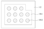
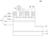
도 2는 실시 예에 의한 자외선 발광 소자(100A)의 평면도를 나타내고, 도 3은 도 2에 예시된 A-A'선을 따라 절취한 단면도를 나타낸다.FIG. 2 is a plan view of the ultraviolet
도 2 및 도 3을 참조하면, 자외선 발광 소자(100A)는 기판(110), 버퍼층(112), 발광 구조물(120), 제1 전극(132), 제2-1 전극(134-1) 및 요부 반사층(134-2)을 포함한다.2 and 3, the ultraviolet
기판(110)은 도전형 물질 또는 비도전형 물질을 포함할 수 있다. 예를 들어, 기판(110)은 사파이어(Al203), AlN, GaN, SiC, ZnO, GaP, InP, Ga203, GaAs 및 Si 중 적어도 하나를 포함할 수 있다.The
기판(110)과 발광 구조물(120) 간의 열 팽창 계수의 차이 및 격자 부정합을 개선하기 위해, 이들(110, 120) 사이에 버퍼층(또는, 전이층)(112)이 배치될 수 있다. 버퍼층(112)은 예를 들어 Al, In, N 및 Ga로 구성되는 군으로부터 선택되는 적어도 하나의 물질을 포함할 수 있으나, 이에 국한되지 않는다. 또한, 버퍼층(112)은 단층 또는 다층 구조를 가질 수도 있다.A buffer layer (or transition layer) 112 may be disposed between the
발광 구조물(120)은 버퍼층(112) 위에 순차적으로 배치된 제1 도전형 반도체층(122), 활성층(124) 및 제2 도전형 반도체층(126)을 포함한다.The
제1 도전형 반도체층(122)은 버퍼층(112) 위에 배치되고, 제1 도전형 도펀트가 도핑된 Ⅲ-Ⅴ 족 또는 Ⅱ-Ⅵ 족 등의 화합물 반도체로 구현될 수 있다. 제1 도전형 반도체층(122)이 n형 반도체층인 경우, 제1 도전형 도펀트는 n형 도펀트로서, Si, Ge, Sn, Se, Te를 포함할 수 있으나 이에 한정되지 않는다.The first
예를 들어, 제1 도전형 반도체층(122)은 AlxInyGa(1-x-y)N (0≤x≤1, 0≤y≤1, 0≤x+y≤1)의 조성식을 갖는 반도체 물질을 포함할 수 있다. 제1 도전형 반도체층(122)은 GaN, InN, AlN, InGaN, AlGaN, InAlGaN, AlInN, AlGaAs, InGaAs, AlInGaAs, GaP, AlGaP, InGaP, AlInGaP, InP 중 어느 하나 이상을 포함할 수 있다.For example, the first conductivity
활성층(124)은 제1 도전형 반도체층(122) 위에 배치되며, 제1 도전형 반도체층(122)을 통해서 주입되는 전자(또는, 정공)와 제2 도전형 반도체층(126)을 통해서 주입되는 정공(또는, 전자)이 서로 만나서, 활성층(124)을 이루는 물질 고유의 에너지 밴드에 의해서 결정되는 에너지를 갖는 빛을 방출하는 층이다.The
활성층(124)은 단일 우물 구조, 다중 우물 구조, 단일 양자 우물 구조, 다중 양자 우물 구조(MQW: Multi Quantum Well), 양자 선(Quantum-Wire) 구조, 또는 양자 점(Quantum Dot) 구조 중 적어도 어느 하나로 형성될 수 있다.The
활성층(124)의 우물층/장벽층은 InGaN/GaN, InGaN/InGaN, GaN/AlGaN, InAlGaN/GaN, GaAs(InGaAs)/AlGaAs, GaP(InGaP)/AlGaP 중 어느 하나 이상의 페어 구조로 형성될 수 있으나 이에 한정되지 않는다. 우물층은 장벽층의 밴드갭 에너지보다 낮은 밴드갭 에너지를 갖는 물질로 형성될 수 있다.The well layer / barrier layer of the
활성층(124)의 위 또는/및 아래에는 도전형 클래드층(미도시)이 형성될 수 있다. 도전형 클래드층은 활성층(124)의 장벽층의 밴드갭 에너지보다 더 높은 밴드갭 에너지를 갖는 반도체로 형성될 수 있다. 예를 들어, 도전형 클래드층은 GaN, AlGaN, InAlGaN 또는 초격자 구조 등을 포함할 수 있다. 또한, 도전형 클래드층은 n형 또는 p형으로 도핑될 수 있다.A conductive clad layer (not shown) may be formed on and / or below the
실시 예에 의하면, 활성층(124)은 자외선 파장 대역의 광을 방출한다. 여기서, 자외선 파장 대역이란, 100 ㎚ 내지 400 ㎚의 파장 대역을 의미한다. 특히, 활성층(124)은 100 ㎚ 내지 280 ㎚ 파장 대역의 광을 방출할 수 있다.According to the embodiment, the
제2 도전형 반도체층(126)은 활성층(124) 위에 배치되며, 반도체 화합물로 형성될 수 있다. 제2 도전형 반도체층(126)은 Ⅲ-Ⅴ 족 또는 Ⅱ-Ⅵ 족 등의 화합물 반도체로 구현될 수 있다. 예컨대, 제2 도전형 반도체층(126)은 InxAlyGa1 -x- yN (0≤x≤1, 0≤y≤1, 0≤x+y≤1)의 조성식을 갖는 반도체 물질을 포함할 수 있다. 제2 도전형 반도체층(126)에는 제2 도전형 도펀트가 도핑될 수 있다. 제2 도전형 반도체층(126)이 p형 반도체층인 경우, 제2 도전형 도펀트는 p형 도펀트로서, Mg, Zn, Ca, Sr, Ba 등을 포함할 수 있다.The second
제1 도전형 반도체층(122)은 n형 반도체층으로, 제2 도전형 반도체층(126)은 p형 반도체층으로 구현할 수 있다. 또는, 제1 도전형 반도체층(122)은 p형 반도체층으로, 제2 도전형 반도체층(126)은 n형 반도체층으로 구현할 수도 있다.The first
발광 구조물(120)은 N-P 접합 구조, P-N 접합 구조, N-P-N 접합 구조, P-N-P 접합 구조 중 어느 한 구조로 구현할 수 있다.The
만일, 활성층(124)에서 자외선 파장 대역의 광을 방출할 경우, 실시 예에 의하면 제2 도전형 반도체층(126)은 제2 도전형 제1 반도체층(126A), 제2 도전형 반사층(126B) 및 제2 도전형 제2 반도체층(126C)을 포함할 수 있다.When the
제2 도전형 제1 반도체층(126A)은 활성층(124) 위에 배치된다. 제2 도전형 제1 반도체층(126A) 및 제1 도전형 반도체층(122) 각각은 AlGaN을 포함할 수 있다. 왜냐하면, AlGaN이 GaN이나 InAlGaN보다 자외선 파장 대역의 광을 덜 흡수하기 때문이다.The second conductive type
만일, 제1 도전형이 n형이고 제2 도전형이 p형인 경우, 제2 도전형 제1 반도체층(126A)은 전자 차단층(EBL:Electron Blocking Layer)의 역할을 수행할 수도 있다. 또는, 이러한 전자 차단층의 역할을 하는 제2 도전형 제1 반도체층(126A)은 AlGaN/AlGaN 초격자층 구조를 가질 수도 있고, AlGaN 벌크 층 구조를 가질 수도 있다.If the first conductive type is n-type and the second conductive type is p-type, the second conductive type
제2 도전형 제2 반도체층(126C)은 제2 도전형 제1 반도체층(126A) 위에 배치된다. 제2 도전형 제2 반도체층(126C)은 제2-1 전극(134-1)으로부터 활성층(124)으로 정공이 원할히 공급되도록 하여 자외선 발광 소자(100A)의 전기적 특성을 개선시키는 역할을 한다. 이를 위해, 제2 도전형 제2 반도체층(126C)은 예를 들어 GaN 또는 InAlGaN을 포함할 수 있다. 그러나, GaN이나 InAlGaN은 AlGaN보다 자외선 파장 대역의 광을 더 많이 흡수하므로 제2 도전형 제2 반도체층(126C)의 존재로 인하여 광 추출 효율이 저하될 수 있다. 이를 방지하기 위해, 제2 도전형 제1 반도체층(126A)과 제2 도전형 제2 반도체층(126C) 사이에 제2 도전형 반사층(126B)을 배치할 수 있다. 제2 도전형 제1 반도체층(126A) 위에 배치되는 제2 도전형 반사층(126B)은 활성층(124)으로부터 방출되는 자외선 파장 대역의 광을 기판(110) 방향으로 반사시키는 역할을 한다. 이를 위해, 제2 도전형 반사층(126B)은 예를 들어 무지향성 반사층(ODR:omni-directional reflector)이나 분산 브래그 반사층(DBR:distributed Bragg reflector) 구조를 가질 수 있다. The second conductive type
여기서, DBR 구조란, "mλ/4n"의 두께로 저굴절율층과 고굴절율층이 교대로 적층된 구조일 수 있다. λ는 활성층(124)에서 방출되는 광의 파장을 나타내고, n은 매질의 굴절율을 나타내고, m은 홀수이다. 저굴절율층은 예를 들어, 실리콘 산화물(SiO2, 굴절율 1.4) 또는 알루미늄 산화물(Al2O3, 굴절율 1.6)을 포함할 수 있으며, 고굴절율층은 예를 들어, 실리콘 질화물(Si3N4, 굴절율 2.05~2.25), 티타늄질화물(TiO2, 굴절률 2 이상) 또는 Si-H(굴절율 3 이상)를 포함할 수 있으나, 실시 예는 이에 국한되지 않는다. 저굴절율층과 고굴절율층의 갯수는 다양하게 변화될 수 있다.Here, the DBR structure may be a structure in which a low refractive index layer and a high refractive index layer are alternately laminated to have a thickness of "m? / 4n ". ? represents the wavelength of light emitted from the
ODR 구조란, 금속 반사층과 그 금속 반사층 상에 저굴절률층이 형성된 구조일 수 있다. 금속 반사층은 Ag 또는 Al일 수 있으며 저굴절률층은 SiO2, Si3N4, MgO와 같은 투명 물질일 수 있다. 또는, ODR 구조란 SiO2층과 TiO2층이 적층된 층을 한 쌍으로 반복적으로 적층된 구조일 수도 있으나, 실시 예는 이에 국한되지 않는다.The ODR structure may be a structure in which a metal reflective layer and a low refractive index layer are formed on the metal reflective layer. A metal reflective layer may be Ag or Al, and a low refractive index layer may be a transparent material such as SiO 2, Si 3 N 4, MgO. Alternatively, the ODR structure may be a structure in which a layer in which a SiO 2 layer and a TiO 2 layer are stacked is repeatedly laminated, but the embodiment is not limited thereto.
제2 도전형 반사층(126B)을 구현하는 ODR이나 DBR은 자외선 파장 대역의 광이 제2 도전형 반사층(126B)으로 입사되는 방향에 따라 다른 반사율을 보인다.The ODR or DBR implementing the second conductive type
도 4a 및 도 4b는 제2 도전형 반사층(126B)의 특성을 예시적으로 나타내는 도면이다. 도 4a는 활성층(124)에서 방출된 광이 제2 도전형 제1 반도체층(126A)을 투과한 후 제2 도전형 반사층(126B)으로 입사되는 방향을 각도(0°, ±15°, ±30°)로 나타내고, 도 4b는 제2 도전형 반사층(126B)의 반사율을 나타내는 그래프로서, 횡축은 자외선 발광 소자(100A)의 가로 방향 위치를 나타내고, 종축은 반사율을 나타낸다.4A and 4B are views showing the characteristics of the second conductive type
만일, 제2 도전형 반사층(126B)이 DBR로 구현될 경우, 도 4a에 예시된 바와 같이 활성층(124)에서 방출된 광이 DBR(126B)로 수직 방향(도 4a의 0°에 해당하고 도 4b의 X=0에 해당한다)으로 입사될 경우, 도 4b에 도시된 바와 같이 DBR(126B)에서의 광 반사율은 최대가 된다. 그러나, 활성층(124)에서 방출된 광이 수직 방향으로부터 멀어지면서 DBR(126B)로 입사될 경우, 도 4b에 도시된 바와 같이 DBR(126B)에서의 광 반사율은 점차 감소하게 되어 광 추출 효율이 낮아질 수 있다. 예를 들어, 광이 30°로 DBR(126B)로 입사될 경우에 DBR(126B)에서의 광 반사율은 15°로 입사될 경우의 광 반사율보다 작아진다.4A, the light emitted from the
전술한 바와 같이, 제2 도전형 반사층(126B)으로 광이 입사되는 방향에 따라 광 반사율이 달라지는 현상을 해소하기 위해, 실시 예에 의하면, 제2 도전형 반사층(126B)과 제2 도전형 제2 반도체층(126C)은 도 2 및 도 3에 예시된 바와 같이 요철부를 포함한다. 여기서, 요철부는 요철 모양의 패턴으로서 요부(GP:Groove Part)(또는, 오목부)와 철부(RP:Rod Part)(또는, 볼록부)를 갖는다. 요부(GP)에서 제2 도전형 제1 반도체층(126A)은 노출된다.As described above, in order to eliminate the phenomenon that the light reflectance varies depending on the direction in which the light is incident on the second conductive
실시 예에 의하면, 요철부에서, 요부(GP)의 폭(W1)은 철부(RP)의 폭(W2)과 다를 수 있다. 예를 들어, W1은 W2보다 클 수 있다. 또한, W1 및 W2 중 적어도 하나는 자외선 발광 소자(100A)의 동작 전압(Vf)을 고려하여 설정될 수 있다.According to the embodiment, in the concavo-convex portion, the width W1 of the concave portion GP may be different from the width W2 of the convex portion RP. For example, W1 may be greater than W2. At least one of W1 and W2 may be set in consideration of the operation voltage Vf of the ultraviolet
한편, 제1 전극(132)은 메사 식각(Mesa etching)에 의해 노출된 제1 도전형 반도체층(122) 위에 배치된다. 제1 전극(132)은 오믹 접촉하는 물질을 포함하여 오믹 역할을 수행하여 별도의 오믹층(미도시)이 배치될 필요가 없을 수도 있고, 별도의 오믹층이 제1 전극(132)의 아래에 배치될 수도 있다.Meanwhile, the
제2-1 전극(134-1)은 철부(RP)의 상부면 위에 배치되고, 요부 반사층(134-2)은 요부(GP)에서 노출된 제2 도전형 제1 반도체층(122) 위에 배치된다.The second-first electrode 134-1 is disposed on the upper surface of the convex portion RP and the concave reflection layer 134-2 is disposed on the second conductive type
전술한 바와 같이, 제2 도전형 반사층(126B)과 제2 도전형 제2 반도체층(126C)이 요철 모양의 패턴을 갖고 제2-1 전극(134-1)과 요부 반사층(134-2)이 배치될 경우, 제2 도전형 반사층(126B)으로 입사되는 광의 방향에 따라 반사율이 달라지는 현상이 감소될 수 있다.As described above, the second conductive type
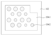
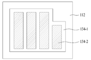
도 5a 내지 도 5d는 실시 예에 의한 요철부의 다양한 평면 형상을 나타낸다.5A to 5D show various planar shapes of the concavo-convex portion according to the embodiment.
도 2에 예시된 제2 도전형 반사층(126B)과 제2 도전형 제2 반도체층(126C)에 형성된 요철부는 사각형 평면 형상이지만, 실시 예는 이에 국한되지 않는다. 즉, 요철부는 도 5a 및 도 5b에 예시된 바와 같이 원형 평면 형상일 수도 있고, 도 5d에 예시된 육각형과 같이 다양한 다각형 평면 형상일 수 있고, 도 5c에 예시된 바와 같이 바(bar) 형태의 평면 형상일 수 있다.Although the concave and convex portions formed in the second conductive type
또한, 도 2, 도 5a, 도 5c 및 도 5d에 예시된 바와 같이 복수의 요부의 크기는 모두 동일할 수도 있고, 도 5b에 예시된 바와 같이 복수의 요부의 크기는 서로 다를 수도 있다.In addition, as illustrated in Figs. 2, 5A, 5C, and 5D, the sizes of the plurality of recesses may be all the same, and the sizes of the plurality of recesses may be different from each other as illustrated in Fig. 5B.
또한, 도 5d에 도시된 요철부의 패턴을 형성하기 위한 식각 공정은 도 2, 도 5a 내지 도 5c에 도시된 요철부의 패턴을 형성하기 위한 식각 공정보다 용이할 수 있다.Further, the etching process for forming the pattern of concave-convex portions shown in Fig. 5D may be easier than the etching process for forming the pattern of concave-convex portions shown in Figs. 2 and 5A to 5C.
도 6은 다른 실시 예에 의한 자외선 발광 소자(100B)의 단면도를 나타낸다.Fig. 6 shows a cross-sectional view of an ultraviolet light-emitting
도 6을 참조하면, 자외선 발광 소자(100B)는 제2-2 전극(134-3)을 더 포함한다. 이를 제외하면 도 6에 예시된 자외선 발광 소자(100B)는 도 2 및 도 3에 예시된 자외선 발광 소자(100A)와 동일하므로 동일한 참조부호를 사용하여 중복되는 설명을 생략한다.Referring to FIG. 6, the ultraviolet
제2-2 전극(134-3)은 요철부에서 철부(RP)의 측면에 배치되어, 제2-1 전극(134-1)과 요부 반사층(134-2)을 서로 전기적으로 연결시킨다. The second -2 electrode 134-3 is disposed on the side surface of the convex portion RP on the convexo-concave portion, and electrically connects the second-1 electrode 134-1 and the concave-convex reflective layer 134-2.
전술한 제1 전극(132), 제2-1 전극(134-1), 요부 반사층(134-2) 및 제2-2 전극(134-3) 각각은 반사성 및 투광성 중 적어도 하나의 성질을 갖는 재질 예를 들어 금속으로 형성될 수 있으며, Ag, Ni, Al, Rh, Pd, Ir, Ru, Mg, Zn, Pt, Au, Hf 및 이들의 선택적인 조합으로 이루어질 수 있다.Each of the
특히, 제2-1 전극(134-1), 요부 반사층(134-2) 및 제2-2 전극(134-3) 각각은 투명 전도성 산화막(TCO:Tranparent Conductive Oxide)일 수도 있다. 예를 들어, 제2-1 전극(134-1), 요부 반사층(134-2) 및 제2-2 전극(134-3) 각각은 전술한 금속 물질과 ITO(indium tin oxide), IZO(indium zinc oxide), IZTO(indium zinc tin oxide), IAZO(indium aluminum zinc oxide), IGZO(indium gallium zinc oxide), IGTO(indium gallium tin oxide), AZO(aluminum zinc oxide), ATO(antimony tin oxide), GZO(gallium zinc oxide), IrOx, RuOx, RuOx/ITO, Ni/IrOx/Au, 및 Ni/IrOx/Au/ITO 중 적어도 하나를 포함할 수 있으며, 이러한 재료로 한정하지는 않는다. 특히 제2-1 전극(134-1)은 제2 도전형 제2 반도체층(126C)과 오믹 접촉하는 물질을 포함할 수 있고, 요부 반사층(134-2)은 제2 도전형 제1 반도체층(126A)과 오믹 접촉하는 물질을 포함할 수 있다.In particular, each of the second-first electrode 134-1, the concave reflection layer 134-2 and the second-electrode 134-3 may be a transparent conductive oxide (TCO). For example, each of the second-1 electrode 134-1, the lobe reflection layer 134-2, and the second -2 electrode 134-3 may be formed of the above-described metal material, ITO (indium tin oxide), IZO zinc oxide (IZTO), indium zinc oxide (IZTO), indium zinc oxide (IZO), indium gallium zinc oxide (IGTO), aluminum zinc oxide (AZO), antimony tin oxide And may include at least one of gallium zinc oxide (GZO), IrOx, RuOx, RuOx / ITO, Ni / IrOx / Au, and Ni / IrOx / Au / ITO. In particular, the second-1 electrode 134-1 may include a material that makes an ohmic contact with the second conductive type
또한, 도 6에 예시된 자외선 발광 소자(100B)에서 제2-1 전극(134-1) 및 요부 반사층(134-2) 각각은 오믹 특성을 갖는 반사 전극 재료로 단층 또는 다층으로 형성될 수 있다. 만일, 제2-1 전극(134-1) 및 요부 반사층(134-2) 각각이 오믹 역할을 수행할 경우, 별도의 오믹층(미도시)은 형성되지 않을 수 있다.In the ultraviolet
도 7은 또 다른 실시 예에 의한 자외선 발광 소자(100C)의 단면도를 나타낸다.Fig. 7 shows a cross-sectional view of an ultraviolet light-emitting
도 7을 참조하면, 자외선 발광 소자(100C)는 요부 반사층(134-2)을 포함하지 않는다. 이를 제외하면 도 7에 예시된 자외선 발광 소자(100C)는 도 2 및 도 3에 예시된 자외선 발광 소자(100A)와 동일하므로 동일한 참조부호를 사용하여 중복되는 설명을 생략한다.Referring to FIG. 7, the ultraviolet
전술한 도 6에 예시된 자외선 발광 소자(100B)에서 제2-2 전극(134-3)에 의해 제2-1 전극(134-1)과 연결되는 요부 반사층(134-2)은 제2 전극(134)의 역할을 수행할 수 있다. 따라서, 도 3 및 도 7에 예시된 자외선 발광 소자(100A, 100C)보다 도 6에 예시된 자외선 발광 소자(100B)에서 제2 전극(134)의 면적이 보다 넓어져서 많은 정공이 활성층(124)으로 제공될 수 있다.In the ultraviolet
전술한 도 3, 도 6 및 도 7에 예시된 자외선 발광 소자(100A, 100B, 100C)는 기판(110)이 제1 도전형 반도체층(122) 아래에 배치되는 수평형 구조이지만, 실시 예는 이에 국한되지 않는다. 즉, 다른 실시 예에 의하면, 자외선 발광 소자는 수직형이나 플립 본딩 구조를 가질 수 있다.The ultraviolet
도 8 내지 도 10은 수직형 구조의 또 다른 실시 예에 의한 자외선 발광 소자(100D, 100E, 100F)의 단면도를 나타낸다.8 to 10 are sectional views of the ultraviolet
도 3, 도 6 및 도 7에 예시된 자외선 발광 소자(100A ~ 100C)는 수평형 구조이므로, 제1 도전형 반도체층(122), 활성층(124), 제2 도전형 제1 반도체층(126A), 제2 도전형 반사층(126B) 및 제2 도전형 제2 반도체층(126C)이 기판(110) 위에 순차적으로 배치된다. 반면에, 도 8 내지 도 10에 예시된 자외선 발광 소자(100D ~ 100F)는 수직형 구조이므로, 제2 도전형 제2 반도체층(126C), 제2 도전형 반사층(126B), 제2 도전형 제1 반도체층(126A), 활성층(124) 및 제1 도전형 반도체층(122)이 지지 기판(140) 위에 순차적으로 배치된다. 이러한 차이점을 제외하면, 도 8 내지 도 10에 예시된 자외선 발광 소자(100D, 100E, 100F) 각각은 도 2, 도 6 및 도 7에 예시된 자외선 발광 소자(100A, 100B, 100C) 각각과 동일하므로 중복되는 설명을 생략한다.The ultraviolet
도 8에 예시된 수직형 본딩 구조의 자외선 발광 소자(100D)는 발광 구조물(120), 제2-1 전극(134-1), 요부 반사층(134-2), 지지 기판(140) 및 제1 전극(142)을 포함한다. 도 9에 예시된 수직형 본딩 구조의 자외선 발광 소자(100E)는 도 8에 예시된 자외선 발광 소자(100D)의 구조에 제2-2 전극(134-3)을 더 포함한다. 도 10에 예시된 수직형 본딩 구조의 자외선 발광 소자(100F)는 도 8에 예시된 자외선 발광 소자(100E)의 구조에서 요부 반사층(134-2)이 생략된다.The ultraviolet
지지 기판(140)은 도전형 물질 또는 비도전형 물질을 포함할 수 있다. 예를 들어, 지지 기판(140)은 사파이어(Al203), GaN, SiC, ZnO, GaP, InP, Ga203, GaAs 및 Si 중 적어도 하나를 포함할 수 있으며, 이에 국한되지 않는다. 만일, 지지 기판(140)이 도전형일 경우, 지지 기판(140) 위에 별도의 전극이 배치되지 않고 지지 기판(140) 전체가 전극의 역할을 할 수 있다. 이를 위해, 지지 기판(140)은 전기 전도도가 우수한 금속을 사용할 수 있고, 발광 소자 작동시 발생하는 열을 충분히 발산시킬 수 있어야 하므로 열전도도가 높은 금속을 사용할 수 있다.The
예를 들어, 지지 기판(140)은 몰리브덴(Mo), 실리콘(Si), 텅스텐(W), 구리(Cu) 및 알루미늄(Al)로 구성되는 군으로부터 선택되는 물질 또는 이들의 합금으로 이루어질 수 있으며, 또한, 금(Au), 구리합금(Cu Alloy), 니켈(Ni), 구리-텅스텐(Cu-W), 캐리어 웨이퍼(예: GaN, Si, Ge, GaAs, ZnO, SiGe, SiC, SiGe, Ga2O3 등) 등을 선택적으로 포함할 수 있다.For example, the
또한, 제1 전극(142)은 도 3, 도 6 및 도 7에 도시된 제1 전극(132)과 마찬가지로 활성층(124)에서 방출된 광을 반사시키는 반사성 물질로 이루어지거나 활성층(124)에서 방출된 광을 투과시키는 투광성 물질로 이루어질 수 있다.The
도 11은 플립 본딩 구조를 갖는 또 다른 실시 예에 의한 자외선 발광 소자(100G)의 단면도를 나타낸다.11 shows a cross-sectional view of an ultraviolet light-emitting
도 11에 예시된 자외선 발광 소자(100G)는 플립 칩 본딩 구조이므로, 서브 마운트(150), 보호층(152), 제1 및 제2 금속층(또는, 전극 패드)(154A, 154B), 제1 및 제2 범프(156A, 156B)를 더 포함한다. 이러한 차이점을 제외하면, 도 11에 예시된 자외선 발광 소자(100G)는 도 3에 예시된 자외선 발광 소자(100A)와 동일하므로 중복되는 부분에 대해서는 동일한 참조부호를 사용하며 이에 대한 상세한 설명을 생략한다.Since the ultraviolet
서브 마운트(150)는 예를 들어 AlN, BN, 탄화규소(SiC), GaN, GaAs, Si 등의 반도체 기판으로 이루어질 수 있으며, 이에 국한되지 않고 열전도도가 우수한 반도체 물질로 이루어질 수도 있다. 또한, 서브 마운트(150) 내에 제너 다이오드 형태의 정전기(ESD:Electro Static Discharge) 방지를 위한 소자가 포함될 수도 있다.The
제1 및 제2 금속층(154A, 154B)은 서브 마운트(150) 위에 수평 방향으로 서로 이격되어 배치된다. 제1 범프(156A)는 제1 금속층(154A)과 제1 전극(132) 사이에 배치되고, 제2 범프(156B)는 제2 금속층(154B)과 제2 전극(134) 사이에 배치된다.The first and
제1 전극(132)은 제1 범프(156A)를 통해 서브 마운트(150)의 제1 금속층(154A)에 연결되며, 제2 전극(134)은 제2 범프(156B)를 통해 서브 마운트(150)의 제2 금속층(154B)에 연결된다.The
비록 도시되지는 않았지만, 제1 전극(132)과 제1 범프(156A) 사이에 제1 상부 범프 금속층(미도시)이 더 배치되고, 제1 금속층(154A)와 제1 범프(156A) 사이에 제1 하부 범프 금속층(미도시)이 더 배치될 수도 있다. 여기서, 제1 상부 범프 금속층과 제1 하부 범프 금속층은 제1 범프(156A)가 위치할 자리를 표시하는 역할을 수행한다. 이와 비슷하게 제2 전극(134)과 제2 범프(156B) 사이에 제2 상부 범프 금속층(미도시)이 더 배치되고, 제2 금속층(154B)와 제2 범프(156B) 사이에 제2 하부 범프 금속층(미도시)이 더 배치될 수도 있다. 여기서, 제2 상부 범프 금속층과 제2 하부 범프 금속층은 제2 범프(156B)가 위치할 자리를 표시하는 역할을 수행한다.Although not shown, a first upper bump metal layer (not shown) is further disposed between the
만일, 서브 마운트(150)가 Si과 같이 전기적 전도성을 갖는 물질로 구현된 경우, 도 11에 예시된 바와 같이 제1 및 제2 금속층(154A, 154B)와 서브 마운트(150) 사이에 보호층(152)이 더 배치될 수도 있다. 여기서, 보호층(152)은 절연 물질로 이루어질 수 있다.If the
이하, 도 3에 예시된 자외선 발광 소자(100A)의 실시 예에 따른 제조 방법을 다음과 같이 살펴본다. 그러나, 도 3에 예시된 자외선 발광 소자(100A)는 이에 국한되지 않고 다른 방법에 의해서도 제조될 수 있음은 물론이다.Hereinafter, a manufacturing method according to an embodiment of the ultraviolet
도 12a 내지 도 12f는 도 3에 예시된 자외선 발광 소자(100A)의 실시 예에 의한 제조 방법을 설명하기 위한 공정 단면도이다.12A to 12F are cross-sectional views illustrating the manufacturing method of the embodiment of the ultraviolet
도 12a를 참조하면, 기판(110) 상에 버퍼층(112)을 형성한다.Referring to FIG. 12A, a
도전성 또는 비도전성 물질에 의해 기판(110)을 형성할 수 있다. 만일, 기판(110)이 실리콘 기판일 경우, 대구경이 용이하며 열전도도가 우수하지만, 실리콘과 질화물계 발광 구조층(120) 간의 열 팽창 계수의 차이 및 격자 부정합에 의해 발광 구조물(120)에 크랙(crack)이 발생하는 등의 문제점이 발생할 수도 있다. 이를 방지하기 위해, 기판(110) 상에 버퍼층(112)을 선택적으로 형성할 수 있다. 버퍼층(112)은 예를 들어 Al, In, N 및 Ga로 구성되는 군으로부터 선택되는 적어도 하나의 물질에 의해 형성할 수 있으나, 이에 국한되지 않는다. 또한, 버퍼층(112)은 단층 또는 다층 구조의 형태로 형성될 수도 있다.The
기판(110) 위에 버퍼층(112)을 형성한 이후, 버퍼층(112) 위에 제1 도전형 반도체층(122), 활성층(124), 제2 도전형 제1 반도체층(126A), 제2 도전형 반사층(126B) 및 제2 도전형 제2 반도체층(126C)을 순차적으로 형성한다.The
제1 도전형 반도체층(122)은 제1 도전형 도펀트가 도핑된 Ⅲ-Ⅴ족 또는 Ⅱ-Ⅵ족 화합물 반도체로 구현될 수 있으며, 제1 도전형 반도체층(122)이 n형 반도체층인 경우, 제1 도전형 도펀트는 n형 도펀트로서, Si, Ge, Sn, Se, Te를 포함할 수 있으나 이에 한정되지 않는다.The first conductivity
제1 도전형 반도체층(122)은 예를 들어, AlxInyGa(1-x-y)N (0≤x≤1, 0≤y≤1, 0≤x+y≤1)의 조성식을 갖는 반도체 물질을 이용하여 형성될 수 있다. 제1 도전형 반도체층(122)은 GaN, InN, AlN, InGaN, AlGaN, InAlGaN, AlInN, AlGaAs, InGaAs, AlInGaAs, GaP, AlGaP, InGaP, AlInGaP, InP 중 어느 하나 이상으로 형성될 수 있다. 전술한 바와 같이, 활성층(124)이 자외선 파장 대역의 광을 방출할 경우, 제1 도전형 반도체층(122)은 AlGaN으로 형성될 수 있다.The first
활성층(124)은 단일 우물 구조, 다중 우물 구조, 단일 양자 우물 구조, 다중 양자 우물 구조, 양자 선 구조, 또는 양자 점 구조 중 적어도 어느 하나로 형성될 수 있다. 예를 들어, 활성층(124)은 트리메틸 갈륨 가스(TMGa), 암모니아 가스(NH3), 질소 가스(N2), 및 트리메틸 인듐 가스(TMIn)가 주입되어 다중 양자우물구조가 형성될 수 있으나 이에 한정되는 것은 아니다.The
활성층(124)의 우물층/장벽층은 InGaN/GaN, InGaN/InGaN, GaN/AlGaN, InAlGaN/GaN, GaAs(InGaAs)/AlGaAs, GaP(InGaP)/AlGaP 중 어느 하나 이상의 페어 구조로 형성될 수 있으나 이에 한정되지 않는다. 우물층은 장벽층의 밴드 갭보다 작은 밴드 갭을 갖는 물질로 형성될 수 있다.The well layer / barrier layer of the
활성층(124)의 위 또는/및 아래에 도전형 클래드층(미도시)이 더 형성될 수 있다. 도전형 클래드층은 활성층(124)의 장벽층의 밴드갭 에너지보다 더 높은 밴드갭 에너지를 갖는 반도체로 형성될 수 있다. 예를 들어, 도전형 클래드층은 GaN, AlGaN, InAlGaN 또는 초격자 구조 등으로 형성될 수 있다. 또한, 도전형 클래드층은 n형 또는 p형으로 도핑될 수 있다.A conductive clad layer (not shown) may be further formed on and / or below the
제2 도전형 제1 및 제2 반도체층(126A, 126C)은 Ⅲ-Ⅴ 족 또는 Ⅱ-Ⅵ 족 등의 화합물 반도체를 이용하여 형성될 수 있으며, 제2 도전형 도펀트가 도핑될 수 있다. 예컨대, InxAlyGa1 -x- yN (0≤x≤1, 0≤y≤1, 0≤x+y≤1)의 조성식을 갖는 반도체 물질을 이용하여 제2 도전형 제1 및 제2 반도체층(126A, 126C)을 형성할 수 있다. 제2 도전형 제1 및 제2 반도체층(126A, 126C)이 p형 반도체층인 경우, 제2 도전형 도펀트는 p형 도펀트로서, Mg, Zn, Ca, Sr, Ba 등을 포함할 수 있다. 만일, 활성층(124)으로부터 자외선 파장 대역의 광이 방출될 경우 제2 도전형 제1 반도체층(126A)은 AlGaN으로 형성되고, 제2 도전형 제2 반도체층(126C)은 GaN 또는 InAlGaN으로 형성될 수 있다.The second conductive type first and
또한, 제2 도전형 반사층(126B)은 DBR 구조 또는 ODR 구조로 형성될 수 있다.In addition, the second conductive type
이후, 도 12b를 참조하면, 제2 도전형 제2 반도체층(126C) 위에 패턴된 포토 레지스트층(160)을 형성하고, 패턴된 포토 레지스트층(160)을 식각 마스크로 이용하여 제2 도전형 제2 반도체층(126C), 제2 도전형 반사층(126B), 제2 도전형 제1 반도체층(126A), 활성층(124) 및 제1 도전형 반도체층(122)을 메사 식각한다.12B, a patterned
메사 식각에 의해 제1 도전형 반도체층(122)을 노출시킨 후, 도 12c에 도시된 바와 같이 포토 레지스트층(160)을 제거한다.After exposing the first
이후, 도 12d에 예시된 바와 같이, 요철 모양의 패턴 즉, 요철부를 형성하기 위해 요부(GP)에 해당하는 부분을 노출시키고, 철부(RP)에 해당하는 부분과 노출된 제1 도전형 반도체층(122)을 덮는 패턴된 포토 레지스트층(162)을 형성한다.Thereafter, as shown in FIG. 12D, a concave-convex pattern, that is, a portion corresponding to the concave portion GP is formed to expose a portion corresponding to the concave portion GP, and a portion corresponding to the convex portion RP, A patterned
이후, 도 12e에 도시된 바와 같이, 포토 레지스트층(162)을 식각 마스크로 이용하여 제2 도전형 제2 반도체층(126C)과 제2 도전형 반사층(126B)을 식각하여 요부(GP)와 철부(RP)를 형성한다.12E, the second conductive type
이후, 도 12f에 도시된 바와 같이, 포토 레지스터층(162)을 제거한다.Thereafter, as shown in Fig. 12F, the
이후, 도 3에 예시된 바와 같이, 노출된 제1 도전형 반도체층(122)의 상부에 제1 전극(132)을 형성함과 동시에 요부(GP)의 저면(GP-1)과 철부(RP)의 상부면(126C-1)에 요부 반사층(134-2) 및 제2-1 전극(134-1)을 각각 형성한다.3, the
예를 들어, 제1 전극(132), 제2-1 전극(134-1) 및 요부 반사층(134-2) 각각은 금속으로 형성될 수 있으며, Ag, Ni, Al, Rh, Pd, Ir, Ru, Mg, Zn, Pt, Au, Hf 및 이들의 선택적인 조합으로 이루어질 수 있다.For example, each of the
특히, 제2-1 전극(134-1) 및 요부 반사층(134-2) 각각은 투명 전도성 산화막(TCO)으로 형성될 수도 있다. 예를 들어, 제2-1 전극(134-1)은 전술한 금속 물질과 ITO(indium tin oxide), IZO(indium zinc oxide), IZTO(indium zinc tin oxide), IAZO(indium aluminum zinc oxide), IGZO(indium gallium zinc oxide), IGTO(indium gallium tin oxide), AZO(aluminum zinc oxide), ATO(antimony tin oxide), GZO(gallium zinc oxide), IrOx, RuOx, RuOx/ITO, Ni/IrOx/Au, 및 Ni/IrOx/Au/ITO 중 적어도 하나에 의해 형성될 수 있으며, 이러한 재료로 한정하지는 않는다.In particular, each of the second-first electrode 134-1 and the lobe reflection layer 134-2 may be formed of a transparent conductive oxide (TCO). For example, the second-1 electrode 134-1 may be formed of the above-described metal material and at least one of ITO (indium tin oxide), IZO (indium zinc oxide), IZTO (indium zinc tin oxide), IAZO IGTO (indium gallium zinc oxide), IGTO (indium gallium tin oxide), AZO (aluminum zinc oxide), ATO (antimony tin oxide), GZO (gallium zinc oxide), IrOx, RuOx, RuOx / ITO, Ni / IrOx / Au , And at least one of Ni / IrOx / Au / ITO, and the material is not limited thereto.
또한, 제2-1 전극(134-1)은 오믹 특성을 갖는 반사 전극 재료로 단층 또는 다층으로 형성될 수 있다. 만일, 제2-1 전극(134-1)이 오믹 역할을 수행할 경우, 별도의 오믹층(미도시)은 형성되지 않을 수 있다.Further, the second-first electrode 134-1 may be formed as a single-layer or multi-layer with a reflective electrode material having an ohmic characteristic. If the second -1 electrode 134-1 performs an ohmic function, a separate ohmic layer (not shown) may not be formed.
전술한 실시 예에 의한 자외선 발광 소자(100A ~ 100G)의 경우, 제2 도전형 반사층(126B)이 입사되는 광의 방향에 따라 다른 반사율을 갖는다고 하더라도, 제2 도전형 반사층(126B)과 제2 도전형 제2 반도체층(126C)에 요철 모양의 패턴인 요철부를 형성하고, 요철부 상에 반사성이나 투광성 물질을 포함하는 제2-1 전극(134-1), 요부 반사층(134-2) 및 제2-2 전극(134-3)을 배치한다. 이 경우, 반사성을 갖는 제2-1 전극(134-1), 요부 반사층(134-2) 및 제2-2 전극(134-3)은 입사되는 광의 방향에 무관하게 광을 반사시킬 수 있기 때문에, 활성층(124)에서 방출된 자외선 대역의 광이 균일하게 반사되도록 하여, 광 추출 효율을 증대시킬 수 있다. 특히, 요부 반사층(134-2)은 입사되는 광의 방향에 무관하게 광을 기판(110) 방향으로 반사시켜 자외선 발광 소자의 외부로 방출되도록 한다.In the case of the ultraviolet
도 13은 실시 예에 따른 발광 소자 패키지(200)의 단면도이다.13 is a cross-sectional view of a light emitting
실시 예에 따른 발광 소자 패키지(200)는 자외선 발광 소자(100G), 기판(210), 제1 및 제2 패키지 몸체(220A, 220B), 절연물(230), 제1 및 제2 와이어(242, 244) 및 몰딩 부재(250)를 포함한다.The light emitting
자외선 발광 소자(100G)는 도 11에 예시된 자외선 발광 소자로서, 동일한 참조부호를 사용하여 이에 대한 상세한 설명을 생략한다. 도 11에 예시된 자외선 발광 소자(100G) 이외에 도 2, 도 6, 도 7, 도 8 내지 도 10에 예시된 자외선 발광 소자(100A ~ 100F) 중 어느 하나가 도 13에 예시된 바와 같이 발광 소자 패키지(200)로 구현될 수 있음은 물론이다.The ultraviolet light-emitting
제1 및 제2 패키지 몸체(220A, 220B)는 기판(210) 위에 배치된다. 여기서, 기판(210)은 인쇄 회로 기판(PCB:Printed Circuit Board)일 수 있으나 이에 국한되지 않는다. 발광 소자(100G)가 자외선 광을 방출할 경우 방열 특성을 향상시키기 위해, 제1 및 제2 패키지 몸체(220A, 220B)는 알루미늄 재질로 구현될 수 있으나 이에 국한되지 않는다.The first and
도 13에서 서브 마운트(150)는 제2 패키지 몸체(220B) 위에 배치된 것으로 도시되어 있지만, 실시 예는 이에 국한되지 않는다. 즉, 서브 마운트(150)는 제2 패키지 몸체(220B)가 아니라 제1 패키지 몸체(220A) 위에 배치될 수도 있다. 자외선 발광 소자(100G)의 제1 및 제2 금속층(154A, 154B)은 제1 및 제2 와이어(242, 244)에 의해 제1 및 제2 패키지 몸체(220A, 220B)에 각각 연결된다. 제1 및 제2 패키지 몸체(220A, 220B)가 전기적 전도성을 갖는 알루미늄 재질로 구현될 경우, 절연물(230)은 제1 패키지 몸체(220A)와 제2 패키지 몸체(220B)를 전기적으로 서로 분리시키는 역할을 한다.Although the
제1 도전형 반도체층(122)은 제1 전극(132), 제1 범프(156A), 제1 금속층(154A), 제1 와이어(242) 및 제1 패키지 몸체(220A)를 통해 기판(210)과 전기적으로 연결될 수 있다. 또한, 제2 도전형 반도체층(126)은 제2 전극(134), 제2 범프(156B), 제2 금속층(154B), 제2 와이어(244) 및 제2 패키지 몸체(220B)를 통해 기판(210)과 전기적으로 연결될 수 있다.The first
몰딩 부재(250)는 제1 및 제2 패키지 몸체(220A, 220B)에 의해 형성된 캐비티에 채워져 자외선 발광 소자(100G)를 포위하여 보호할 수 있다. 또한, 몰딩 부재(250)는 형광체를 포함하여, 자외선 발광 소자(100G)에서 방출된 광의 파장을 변화시킬 수 있다.The
다른 실시 예에 따른 발광 소자 패키지는 복수 개가 기판 상에 어레이되며, 발광 소자 패키지에서 방출되는 광의 경로 상에 광학 부재인 도광판, 프리즘 시트, 확산 시트, 형광 시트 등이 배치될 수 있다. 이러한 발광 소자 패키지, 기판, 광학 부재는 살균 장치에 이용되거나 백라이트 유닛으로 기능하거나 조명 유닛으로 기능할 수 있으며, 예를 들어, 조명 시스템은 백라이트 유닛, 조명 유닛, 지시 장치, 램프, 가로등을 포함할 수 있다.A plurality of light emitting device packages according to other embodiments may be arranged on a substrate, and a light guide plate, a prism sheet, a diffusion sheet, a fluorescent sheet, or the like may be disposed on a path of light emitted from the light emitting device package. The light emitting device package, the substrate, and the optical member may be used in a sterilizing apparatus, function as a backlight unit, or function as a lighting unit. For example, the lighting system may include a backlight unit, a lighting unit, .
도 14는 실시 예에 따른 발광 소자 패키지를 포함하는 공기 살균 장치(500)의 사시도를 나타낸다.14 is a perspective view of an
도 14를 참조하면, 공기 살균 장치(500)는, 케이싱(501)의 일면에 실장된 발광 모듈부(510)와, 방출된 자외선 파장 대역의 광을 난반사시키는 난반사 반사 부재(530a, 530b)와, 발광 모듈부(510)에서 필요한 가용전력을 공급하는 전원 공급부(520)를 포함한다.14, the
먼저 케이싱(501)은 장방형 구조로 이루어지며 발광 모듈부(510)와 난반사 반사부재(530a, 530b) 및 전원 공급부(520)를 모두 내장하는 일체형 즉 콤팩트한 구조로 형성될 수 있다. 또한, 케이싱(501)은 공기 살균 장치(500) 내부에서 발생된 열을 외부로 방출시키기에 효과적인 재질 및 형상을 가질 수 있다. 예를 들어, 케이싱(501)의 재질은 Al, Cu 및 이들의 합금 중 어느 하나의 재질로 이루어 질 수 있다. 따라서, 케이싱(501)의 외기와의 열전달 효율이 향상되어, 방열 특성이 개선될 수 있다.First, the
또는, 케이싱(501)은 특유한 외부 표면 형상을 가질 수 있다. 예를 들어, 케이싱(501)은 예를 들어 코러게이션(corrugation) 또는 메쉬(mesh) 또는 불특정 요철 무늬 형상으로 돌출 형성되는 외부 표면 형상을 가질 수 있다. 따라서, 케이싱(501)의 외기와의 열전달 효율이 더욱 향상되어 방열 특성이 개선될 수 있다.Alternatively, the
한편, 이러한 케이싱(501)의 양단에는 부착판(550)이 더 배치될 수 있다. 부착판(550)은 도 14에 예시된 바와 같이 케이싱(501)을 전체 설비 장치에 구속시켜 고정하는데 사용되는 브라켓 기능의 부재를 의미한다. 이러한 부착판(550)은 케이싱(501)의 양단에서 일측 방향으로 돌출 형성될 수 있다. 여기서, 일측 방향은 심자외선이 방출되고 난반사가 일어나는 케이싱(501)의 내측 방향일 수 있다.On the other hand,
따라서, 케이싱(501)으로부터 양단 상에 구비된 부착판(550)은 전체 설비 장치와의 고정 영역을 제공하여, 케이싱(501)이 보다 효과적으로 고정 설치될 수 있도록 한다.Thus, the
부착판(550)은 나사 체결 수단, 리벳 체결 수단, 접착 수단 및 탈착 수단 중 어느 하나의 형태를 가질 수 있으며, 이들 다양한 결합 수단의 방식은 당업자의 수준에서 자명하므로, 여기서 상세한 설명은 생략하기로 한다.The
한편, 발광 모듈부(510)는 전술한 케이싱(501)의 일면 상에 실장 되는 형태로 배치된다. 발광 모듈부(510)는 공기 중의 미생물을 살균 처리하도록 자외선 특히 심자외선 광을 방출하는 역할을 한다. 이를 위해, 발광 모듈부(510)는 기판(512)과, 기판(512)에 탑재된 다수의 발광 소자 패키지(200)를 포함한다. 여기서, 발광 소자 패키지(200)는 도 13에 예시된 발광 소자 패키지(200)에 해당할 수 있으나 이에 국한되지 않는다.On the other hand, the light emitting
기판(512)은 케이싱(501)의 내면을 따라 단일 열로 배치되어 있으며, 회로 패턴(미도시)을 포함하는 PCB일 수 있다. 다만, 기판(512)은 일반 PCB 뿐 아니라, 메탈 코어 PCB(MCPCB, Metal Core PCB), 연성(flexible) PCB 등을 포함할 수도 있으며, 이에 대해 한정하지는 않는다. 여기서, 기판(512)은 도 13에 예시된 기판(210)에 해당할 수 있다.The
다음으로, 난반사 반사부재(530a, 530b)는 전술한 발광 모듈부(510)에서 방출된 심자외선 광을 강제로 난반사시키도록 형성되는 반사판 형태의 부재를 의미한다. 이러한 난반사 반사부재(530a, 530b)의 전면 형상 및 배치 형상은 다양한 형상을 가질 수 있다. 난반사 반사부재(530a, 530b)의 면상 구조(예: 곡률반경 등)를 조금씩 변경하여 설계함에 따라, 난반사된 심자외선이 중첩되게 조사되어 조사 강도가 강해지거나, 또는 조사 영역되는 영역의 폭이 확장될 수 있다.Next, the diffuse
전원 공급부(520)는 전원을 도입 받아 전술된 발광 모듈부(510)에서 필요한 가용전력을 공급하는 역할을 한다. 이러한 전원 공급부(520)는 전술한 케이싱(501) 내에 배치될 수 있다. 도 14에 예시된 바와 같이, 전원 공급부(520)는 난반사 반사부재(530a, 530b)와 발광 모듈부(510) 사이의 이격 공간의 내벽 쪽에 배치될 수 있다. 외부 전원을 전원 공급부(520) 측으로 도입시키기 위해 상호 간을 전기적으로 연결하는 전원 연결부(540)가 더 배치될 수 있다.The
도 14에 예시된 바와 같이, 전원 연결부(540)의 형태는 면상일 수 있으나, 외부의 전원 케이블(미도시)이 전기적으로 접속될 수 있는 소켓 또는 케이블 슬롯의 형태를 가질 수 있다. 그리고 전원 케이블은 플렉시블한 연장 구조를 가져, 외부 전원과의 연결이 용이한 형태로 이루어질 수 있다.As illustrated in FIG. 14, the
도 15는 실시 예에 따른 발광 소자 패키지를 포함하는 표시 장치(800)를 나타낸다.15 shows a
도 15를 참조하면, 표시 장치(800)는 바텀 커버(810)와, 바텀 커버(810) 상에 배치되는 반사판(820)과, 광을 방출하는 발광 모듈(830, 835)과, 반사판(820)의 전방에 배치되며 발광 모듈(830, 835)에서 발산되는 빛을 표시 장치 전방으로 안내하는 도광판(840)과, 도광판(840)의 전방에 배치되는 프리즘 시트들(850, 860)을 포함하는 광학 시트와, 광학 시트 전방에 배치되는 디스플레이 패널(870)과, 디스플레이 패널(870)과 연결되고 디스플레이 패널(870)에 화상 신호를 공급하는 화상 신호 출력 회로(872)와, 디스플레이 패널(870)의 전방에 배치되는 컬러 필터(880)를 포함할 수 있다. 여기서, 바텀 커버(810), 반사판(820), 발광 모듈(830,835), 도광판(840) 및 광학 시트는 백라이트 유닛(Backlight Unit)을 이룰 수 있다.15, the
발광 모듈은 기판(830) 상에 실장되는 발광 소자 패키지들(835)을 포함할 수 있다. 여기서, 기판(830)은 PCB 등이 사용될 수 있다. 기판(830)과 발광 소자 패키지(835)는 도 13에 도시된 실시 예(200)일 수 있다.The light emitting module may include light emitting device packages 835 mounted on the
바텀 커버(810)는 표시 장치(800) 내의 구성 요소들을 수납할 수 있다. 그리고, 반사판(820)은 본 도면처럼 별도의 구성요소로 마련될 수도 있으며, 도광판(840)의 후면이나, 바텀 커버(810)의 전면에 반사도가 높은 물질로 코팅되는 형태로 마련되는 것도 가능하다.The
여기서, 반사판(820)은 반사율이 높고 초박형으로 사용 가능한 소재를 사용할 수 있고, 폴리에틸렌 테레프탈레이트(PolyEthylene Terephtalate; PET)를 사용할 수 있다.Here, the
그리고, 도광판(840)은 폴리메틸메타크릴레이트(PolyMethylMethAcrylate; PMMA), 폴리카보네이트(PolyCarbonate; PC), 또는 폴리에틸렌(PolyEthylene; PE) 등으로 형성될 수 있다.The
그리고, 제1 프리즘 시트(850)는 지지 필름의 일면에, 투광성이면서 탄성을 갖는 중합체 재료로 형성될 수 있으며, 중합체는 복수 개의 입체구조가 반복적으로 형성된 프리즘층을 가질 수 있다. 여기서, 복수 개의 패턴은 도시된 바와 같이 마루와 골이 반복적으로 스트라이프 타입으로 구비될 수 있다.The
그리고, 제2 프리즘 시트(860)에서 지지 필름 일면의 마루와 골의 방향은, 제1 프리즘 시트(850) 내의 지지필름 일면의 마루와 골의 방향과 수직할 수 있다. 이는 발광 모듈과 반사 시트로부터 전달된 빛을 디스플레이 패널(870)의 전면으로 고르게 분산하기 위함이다.In the
그리고, 도시되지는 않았으나, 도광판(840)과 제1 프리즘 시트(850) 사이에 확산 시트가 배치될 수 있다. 확산 시트는 폴리에스터와 폴리카보네이트 계열의 재료로 이루어질 수 있으며, 백라이트 유닛으로부터 입사된 빛을 굴절과 산란을 통하여 광 투사각을 최대로 넓힐 수 있다. 그리고, 확산 시트는 광확산제를 포함하는 지지층과, 광출사면(제1 프리즘 시트 방향)과 광입사면(반사시트 방향)에 형성되며 광확산제를 포함하지 않는 제1 레이어와 제2 레이어를 포함할 수 있다.Although not shown, a diffusion sheet may be disposed between the
실시 예에서 확산 시트, 제1 프리즘시트(850), 및 제2 프리즘시트(860)가 광학 시트를 이루는데, 광학 시트는 다른 조합 예를 들어, 마이크로 렌즈 어레이로 이루어지거나 확산 시트와 마이크로 렌즈 어레이의 조합 또는 하나의 프리즘 시트와 마이크로 렌즈 어레이의 조합 등으로 이루어질 수 있다.In an embodiment, the diffusion sheet, the
디스플레이 패널(870)에 액정 표시 패널(Liquid crystal display)이 배치될 수 있는데, 액정 표시 패널 외에 광원을 필요로 하는 다른 종류의 표시 장치가 구비될 수 있다.A liquid crystal display (LCD) panel may be disposed on the
도 16은 실시 예에 따른 발광 소자 패키지를 포함하는 헤드 램프(head lamp, 900)를 나타낸다.16 shows a
도 16을 참조하면, 헤드 램프(900)는 발광 모듈(901), 리플렉터(reflector, 902), 쉐이드(903) 및 렌즈(904)를 포함한다.16, the
발광 모듈(901)은 기판(미도시) 상에 배치되는 복수의 발광 소자 패키지들(미도시)을 포함할 수 있다. 이때 발광 소자 패키지는 도 13에 도시된 실시 예(200)일 수 있다.The
리플렉터(902)는 발광 모듈(901)로부터 조사되는 빛(911)을 일정 방향, 예컨대, 전방(912)으로 반사시킨다.The
쉐이드(903)는 리플렉터(902)와 렌즈(904) 사이에 배치되며, 리플렉터(902)에 의하여 반사되어 렌즈(904)로 향하는 빛의 일부분을 차단 또는 반사하여 설계자가 원하는 배광 패턴을 이루도록 하는 부재로서, 쉐이드(903)의 일측부(903-1)와 타측부(903-2)는 서로 높이가 다를 수 있다.The
발광 모듈(901)로부터 조사되는 빛은 리플렉터(902) 및 쉐이드(903)에서 반사된 후 렌즈(904)를 투과하여 차체 전방을 향할 수 있다. 렌즈(904)는 리플렉터(902)에 의하여 반사된 빛을 전방으로 굴절시킬 수 있다.The light emitted from the
도 17은 실시 예에 따른 발광 소자 또는 발광 소자 패키지를 포함하는 조명 장치(1000)를 나타낸다.17 shows a
도 17을 참조하면, 조명 장치(1000)는 커버(1100), 광원 모듈(1200), 방열체(1400), 전원 제공부(1600), 내부 케이스(1700) 및 소켓(1800)을 포함할 수 있다. 또한, 실시 예에 따른 조명 장치(1000)는 부재(1300)와 홀더(1500) 중 어느 하나 이상을 더 포함할 수 있다.17, the
광원 모듈(1200)은 도 3, 도 6 내지 도 11에 예시된 발광 소자(100A ~ 100G), 또는 도 13에 도시된 발광 소자 패키지(200)를 포함할 수 있다.The
커버(1100)는 벌브(bulb) 또는 반구의 형상일 수 있으며, 속이 비어 있고, 일 부분이 개구된 형상일 수 있다. 커버(1100)는 광원 모듈(1200)과 광학적으로 결합될 수 있다. 예를 들어, 커버(1100)는 광원 모듈(1200)로부터 제공되는 빛을 확산, 산란 또는 여기시킬 수 있다. 커버(1100)는 일종의 광학 부재일 수 있다. 커버(1100)는 방열체(1400)와 결합될 수 있다. 커버(1100)는 방열체(1400)와 결합하는 결합부를 가질 수 있다.The
커버(1100)의 내면에는 유백색 도료가 코팅될 수 있다. 유백색의 도료는 빛을 확산시키는 확산재를 포함할 수 있다. 커버(1100)의 내면의 표면 거칠기는 커버(1100)의 외면의 표면 거칠기보다 크게 형성될 수 있다. 이는 광원 모듈(1200)로부터의 빛이 충분히 산란 및 확산되어 외부로 방출시키기 위함이다.The inner surface of the
커버(1100)의 재질은 유리(glass), 플라스틱, 폴리프로필렌(PP), 폴리에틸렌(PE), 폴리카보네이트(PC) 등일 수 있다. 여기서, 폴리카보네이트는 내광성, 내열성, 강도가 뛰어나다. 커버(1100)는 외부에서 광원 모듈(1200)이 보이도록 투명할 수 있으나, 이에 한정되는 것은 아니고 불투명할 수 있다. 커버(1100)는 블로우(blow) 성형을 통해 형성될 수 있다.The
광원 모듈(1200)은 방열체(1400)의 일 면에 배치될 수 있으며, 광원 모듈(1200)로부터 발생한 열은 방열체(1400)로 전도될 수 있다. 광원 모듈(1200)은 광원부(1210), 연결 플레이트(1230) 및 커넥터(1250)를 포함할 수 있다.The
부재(1300)는 방열체(1400)의 상면 위에 배치될 수 있고, 복수의 광원부(1210)와 커넥터(1250)가 삽입되는 가이드홈(1310)을 갖는다. 가이드홈(1310)은 광원부(1210)의 기판 및 커넥터(1250)와 대응 또는 정렬될 수 있다.The
부재(1300)의 표면은 광 반사 물질로 도포 또는 코팅된 것일 수 있다.The surface of the
예를 들면, 부재(1300)의 표면은 백색의 도료로 도포 또는 코팅된 것일 수 있다. 이러한 부재(1300)는 커버(1100)의 내면에 반사되어 광원 모듈(1200)을 향하여 되돌아오는 빛을 다시 커버(1100) 방향으로 반사할 수 있다. 따라서, 실시 예에 따른 조명 장치의 광 효율을 향상시킬 수 있다.For example, the surface of the
부재(1300)는 예로서 절연 물질로 이루어질 수 있다. 광원 모듈(1200)의 연결 플레이트(1230)는 전기 전도성의 물질을 포함할 수 있다. 따라서, 방열체(1400)와 연결 플레이트(1230) 사이에 전기적인 접촉이 이루어질 수 있다. 부재(1300)는 절연 물질로 구성되어 연결 플레이트(1230)와 방열체(1400)의 전기적 단락을 차단할 수 있다. 방열체(1400)는 광원 모듈(1200)로부터의 열과 전원 제공부(1600)로부터의 열을 전달받아 방열할 수 있다.The
홀더(1500)는 내부 케이스(1700)의 절연부(1710)의 수납홈(1719)을 막는다. 따라서, 내부 케이스(1700)의 절연부(1710)에 수납되는 전원 제공부(1600)는 밀폐될 수 있다. 홀더(1500)는 가이드 돌출부(1510)를 가질 수 있으며, 가이드 돌출부(1510)는 전원 제공부(1600)의 돌출부(1610)가 관통하는 홀을 가질 수 있다.The
전원 제공부(1600)는 외부로부터 제공받은 전기적 신호를 처리 또는 변환하여 광원 모듈(1200)로 제공한다. 전원 제공부(1600)는 내부 케이스(1700)의 수납홈(1719)에 수납될 수 있고, 홀더(1500)에 의해 내부 케이스(1700)의 내부에 밀폐될 수 있다. 전원 제공부(1600)는 돌출부(1610), 가이드부(1630), 베이스(1650) 및 연장부(1670)를 포함할 수 있다.The
가이드부(1630)는 베이스(1650)의 일 측에서 외부로 돌출된 형상을 가질 수 있다. 가이드부(1630)는 홀더(1500)에 삽입될 수 있다. 베이스(1650)의 일 면 위에는 다수의 부품이 배치될 수 있다. 다수의 부품은 예를 들어, 외부 전원으로부터 제공되는 교류 전원을 직류 전원으로 변환하는 직류변환장치, 광원 모듈(1200)의 구동을 제어하는 구동칩, 광원 모듈(1200)을 보호하기 위한 ESD(ElectroStatic discharge) 보호 소자 등을 포함할 수 있으나 이에 대해 한정하지는 않는다.The
연장부(1670)는 베이스(1650)의 다른 일 측에서 외부로 돌출된 형상을 가질 수 있다. 연장부(1670)는 내부 케이스(1700)의 연결부(1750) 내부에 삽입될 수 있고, 외부로부터의 전기적 신호를 제공받을 수 있다. 예컨대, 연장부(1670)는 내부 케이스(1700)의 연결부(1750)와 폭이 같거나 작을 수 있다. 연장부(1670)에는 "+ 전선"과 "- 전선"의 각 일 단이 전기적으로 연결될 수 있고, "+ 전선"과 "- 전선"의 다른 일 단은 소켓(1800)에 전기적으로 연결될 수 있다.The
내부 케이스(1700)는 내부에 전원 제공부(1600)와 함께 몰딩부를 포함할 수 있다. 몰딩부는 몰딩 액체가 굳어진 부분으로서, 전원 제공부(1600)가 내부 케이스(1700) 내부에 고정될 수 있도록 한다.The
이상에서 실시 예를 중심으로 설명하였으나 이는 단지 예시일 뿐 본 발명을 한정하는 것이 아니며, 본 발명이 속하는 분야의 통상의 지식을 가진 자라면 본 실시 예의 본질적인 특성을 벗어나지 않는 범위에서 이상에 예시되지 않은 여러 가지의 변형과 응용이 가능함을 알 수 있을 것이다. 예를 들어, 실시 예에 구체적으로 나타난 각 구성 요소는 변형하여 실시할 수 있는 것이다. 그리고 이러한 변형과 응용에 관계된 차이점들은 첨부된 청구 범위에서 규정하는 본 발명의 범위에 포함되는 것으로 해석되어야 할 것이다.While the present invention has been particularly shown and described with reference to exemplary embodiments thereof, it is to be understood that the invention is not limited to the disclosed exemplary embodiments, but, on the contrary, It will be understood that various modifications and applications are possible. For example, each component specifically shown in the embodiments can be modified and implemented. It is to be understood that all changes and modifications that come within the meaning and range of equivalency of the claims are therefore intended to be embraced therein.
10, 110: 기판 20, 120: 발광 구조물
100A ~ 100G: 자외선 발광 소자 112: 버퍼층
122: 제1 도전형 반도체층 124: 활성층
126A: 제2 도전형 제1 반도체층 126B: 제2 도전형 반사층
126C: 제2 도전형 제2 반도체층 132, 142: 제1 전극
134-1: 제2-1 전극 134-2: 요부 반사층
134-3: 제2-2 전극 140: 지지 기판
150: 서브 마운트 152: 보호층
154A, 154B: 금속층 156A, 156B: 범프
200: 발광 소자 패키지 210: 기판
220A, 220B: 패키지 몸체 230: 절연물
242, 244: 와이어 250: 몰딩 부재
500: 공기 살균 장치 501: 케이싱
510: 발광 모듈부 530a, 530b: 난반사 반사 부재
520: 전원 공급부 800: 표시 장치
810: 바텀 커버 820: 반사판
830, 835, 901: 발광 모듈 840: 도광판
850, 860: 프리즘 시트 870: 디스플레이 패널
872: 화상 신호 출력 회로 880: 컬러 필터
900: 헤드 램프 902: 리플렉터
903: 쉐이드 904: 렌즈
1000: 조명 장치 1100: 커버
1200: 광원 모듈 1400: 방열체
1600: 전원 제공부 1700: 내부 케이스
1800: 소켓10, 110:
100A to 100G: ultraviolet light emitting device 112: buffer layer
122: first conductivity type semiconductor layer 124: active layer
126A: second conductive type
126C: second conductive type
134-1: second electrode 1: electrode 134-2:
134-3: second -2 electrode 140: supporting substrate
150: Sub mount 152: Protective layer
154A, 154B:
200: light emitting device package 210: substrate
220A, 220B: package body 230: insulator
242, 244: wire 250: molding member
500: air sterilizer 501: casing
510: light emitting
520: Power supply unit 800: Display device
810: bottom cover 820: reflector
830, 835, 901: light emitting module 840: light guide plate
850, 860: prism sheet 870: display panel
872: Image signal output circuit 880: Color filter
900: Headlamp 902: Reflector
903: Shade 904: Lens
1000: illumination device 1100: cover
1200: light source module 1400: heat sink
1600: power supply unit 1700: inner case
1800: Socket
Claims (12)
상기 제1 도전형 반도체층 위에 배치되며, 자외선 파장 대역의 광을 방출하는 활성층;
상기 활성층 위에 배치된 제2 도전형 제1 반도체층;
상기 제2 도전형 제1 반도체층 위에 배치되며, 상기 활성층으로부터 방출된 광이 입사되는 방향에 따른 다른 반사율로 상기 광을 반사시키는 제2 도전형 반사층; 및
상기 제2 도전형 반사층 위에 배치되는 제2 도전형 제2 반도체층을 포함하고,
상기 제2 도전형 반사층과 상기 제2 도전형 제2 반도체층은 요철부를 포함하고, 상기 요부는 상기 제2 도전형 제1 반도체층을 노출시키는 자외선 발광 소자.A first conductive semiconductor layer;
An active layer disposed on the first conductive semiconductor layer and emitting light in an ultraviolet wavelength band;
A second conductive type first semiconductor layer disposed on the active layer;
A second conductive type reflective layer disposed on the second conductive type first semiconductor layer and reflecting the light with a different reflectance according to a direction in which light emitted from the active layer is incident; And
And a second conductive type second semiconductor layer disposed on the second conductive type reflective layer,
The second conductive type reflective layer and the second conductive type second semiconductor layer include concave and convex portions, and the concave portion exposes the second conductive type first semiconductor layer.
상기 제1 도전형 반도체층 위에 배치된 제1 전극; 및
상기 철부의 상부면 위에 배치되는 제2-1 전극을 더 포함하는 자외선 발광 소자.The organic electroluminescent device according to claim 1, wherein the ultraviolet light-
A first electrode disposed on the first conductive semiconductor layer; And
And a second-1 electrode disposed on the upper surface of the convex portion.
상기 제1 도전형 반도체층, 상기 활성층, 상기 제2 도전형 제1 반도체층, 상기 제2 도전형 반사층 및 상기 제2 도전형 제2 반도체층은 상기 기판 위에 순차적으로 배치된 자외선 발광 소자.2. The apparatus of claim 1, further comprising a substrate,
Wherein the first conductivity type semiconductor layer, the active layer, the second conductivity type first semiconductor layer, the second conductivity type reflection layer, and the second conductivity type second semiconductor layer are sequentially disposed on the substrate.
상기 제2 도전형 제2 반도체층, 상기 제2 도전형 반사층, 상기 제2 도전형 제1 반도체층, 상기 활성층 및 상기 제1 도전형 반도체층은 상기 지지 기판 위에 순차적으로 배치된 자외선 발광 소자.3. The apparatus of claim 2, further comprising a support substrate,
Wherein the second conductive type second semiconductor layer, the second conductive type reflective layer, the second conductive type first semiconductor layer, the active layer, and the first conductive type semiconductor layer are sequentially disposed on the supporting substrate.
서브 마운트;
상기 서브 마운트 위에 수평 방향으로 서로 이격되어 배치된 제1 및 제2 금속층;
상기 제1 금속층과 상기 제1 전극 사이에 배치된 제1 범프; 및
상기 제2 금속층과 상기 제2-1 전극 사이에 배치된 제2 범프를 더 포함하는 자외선 발광 소자.The organic electroluminescent device according to claim 2, wherein the ultraviolet light-
Submount;
First and second metal layers disposed horizontally spaced apart from each other on the submount;
A first bump disposed between the first metal layer and the first electrode; And
And a second bump disposed between the second metal layer and the second electrode.
상기 제2 도전형 제2 반도체층은 GaN 또는 InAlGaN을 포함하는 자외선 발광 소자.The method of claim 1, wherein each of the first conductive type semiconductor layer and the second conductive type first semiconductor layer includes AlGaN,
And the second conductive type second semiconductor layer comprises GaN or InAlGaN.
Priority Applications (1)
| Application Number | Priority Date | Filing Date | Title |
|---|---|---|---|
| KR1020130093616A KR102076241B1 (en) | 2013-08-07 | 2013-08-07 | Ultraviolet Light Emitting Device |
Applications Claiming Priority (1)
| Application Number | Priority Date | Filing Date | Title |
|---|---|---|---|
| KR1020130093616A KR102076241B1 (en) | 2013-08-07 | 2013-08-07 | Ultraviolet Light Emitting Device |
Publications (2)
| Publication Number | Publication Date |
|---|---|
| KR20150017543A true KR20150017543A (en) | 2015-02-17 |
| KR102076241B1 KR102076241B1 (en) | 2020-02-12 |
Family
ID=53046357
Family Applications (1)
| Application Number | Title | Priority Date | Filing Date |
|---|---|---|---|
| KR1020130093616A KR102076241B1 (en) | 2013-08-07 | 2013-08-07 | Ultraviolet Light Emitting Device |
Country Status (1)
| Country | Link |
|---|---|
| KR (1) | KR102076241B1 (en) |
Cited By (5)
| Publication number | Priority date | Publication date | Assignee | Title |
|---|---|---|---|---|
| WO2017011474A1 (en) * | 2015-07-13 | 2017-01-19 | Sensor Electronic Technology, Inc. | P-type contact to semiconductor heterostructure |
| WO2017034167A1 (en) * | 2015-08-24 | 2017-03-02 | 엘지이노텍(주) | Light emitting element |
| KR20180010117A (en) * | 2016-07-20 | 2018-01-30 | 엘지이노텍 주식회사 | Semiconductor device |
| US10236415B2 (en) | 2015-07-13 | 2019-03-19 | Sensor Electronic Technology, Inc. | P-type contact to semiconductor heterostructure |
| US10333025B1 (en) | 2017-12-19 | 2019-06-25 | Samsung Electronics Co., Ltd. | Ultraviolet light emitting devices having a dielectric layer and a transparent electrode layer disposed in between patterned nitride semiconductor layers |
Citations (2)
| Publication number | Priority date | Publication date | Assignee | Title |
|---|---|---|---|---|
| KR20060014608A (en) * | 2004-08-11 | 2006-02-16 | 삼성전기주식회사 | Nitride semiconductor light emitting diode and method of producing the same |
| KR20110106347A (en) * | 2008-12-08 | 2011-09-28 | 크리 인코포레이티드 | Composite high reflectivity layer |
-
2013
- 2013-08-07 KR KR1020130093616A patent/KR102076241B1/en active IP Right Grant
Patent Citations (2)
| Publication number | Priority date | Publication date | Assignee | Title |
|---|---|---|---|---|
| KR20060014608A (en) * | 2004-08-11 | 2006-02-16 | 삼성전기주식회사 | Nitride semiconductor light emitting diode and method of producing the same |
| KR20110106347A (en) * | 2008-12-08 | 2011-09-28 | 크리 인코포레이티드 | Composite high reflectivity layer |
Cited By (9)
| Publication number | Priority date | Publication date | Assignee | Title |
|---|---|---|---|---|
| WO2017011474A1 (en) * | 2015-07-13 | 2017-01-19 | Sensor Electronic Technology, Inc. | P-type contact to semiconductor heterostructure |
| US9859461B2 (en) | 2015-07-13 | 2018-01-02 | Sensor Electronic Technology, Inc. | P-type contact to semiconductor heterostructure |
| US10236415B2 (en) | 2015-07-13 | 2019-03-19 | Sensor Electronic Technology, Inc. | P-type contact to semiconductor heterostructure |
| WO2017034167A1 (en) * | 2015-08-24 | 2017-03-02 | 엘지이노텍(주) | Light emitting element |
| US10763394B2 (en) | 2015-08-24 | 2020-09-01 | Lg Innotek Co., Ltd. | Light emitting element having excellent contact between semiconductor layer and electrode |
| US11018279B2 (en) | 2015-08-24 | 2021-05-25 | Lg Innotek Co., Ltd. | Light emitting element having excellent contact between semiconductor layer and electrode |
| KR20180010117A (en) * | 2016-07-20 | 2018-01-30 | 엘지이노텍 주식회사 | Semiconductor device |
| US10333025B1 (en) | 2017-12-19 | 2019-06-25 | Samsung Electronics Co., Ltd. | Ultraviolet light emitting devices having a dielectric layer and a transparent electrode layer disposed in between patterned nitride semiconductor layers |
| KR20190073908A (en) * | 2017-12-19 | 2019-06-27 | 삼성전자주식회사 | Ultraviolet semiconductor light emitting devices |
Also Published As
| Publication number | Publication date |
|---|---|
| KR102076241B1 (en) | 2020-02-12 |
Similar Documents
| Publication | Publication Date | Title |
|---|---|---|
| US9929327B2 (en) | Light-emitting device package and light-emitting module including the same | |
| JP6516995B2 (en) | Light emitting device, light emitting device package including the same, and lighting apparatus including the package | |
| KR102080778B1 (en) | Light emitting device package | |
| KR20150131641A (en) | Light emitting device and light emitting device package including the device | |
| KR20150012950A (en) | Light Emitting Device Package | |
| KR102076241B1 (en) | Ultraviolet Light Emitting Device | |
| KR102066620B1 (en) | A light emitting device | |
| KR102182024B1 (en) | A light emitting device | |
| KR102050056B1 (en) | Light Emitting Device | |
| KR20150001268A (en) | Light emitting device package | |
| KR20160014263A (en) | Light emitting device and light emitting device package | |
| KR102170216B1 (en) | Light emitting device and light emitting device package | |
| KR102114935B1 (en) | Light emitting device module | |
| KR102114932B1 (en) | Light emitting device and package including the device | |
| KR102140273B1 (en) | Light emitting device and light emitting device package including the same | |
| KR20150029920A (en) | Light Emitting Device and Light Emitting Device Package | |
| KR20190035648A (en) | Light emitting device package | |
| KR102194804B1 (en) | Light emitting device | |
| KR20150091922A (en) | Light Emitting Device and Light Emitting Device Package | |
| KR20150040630A (en) | Light Emitting Device | |
| KR102050057B1 (en) | Light Emitting Device Package | |
| KR20160055439A (en) | Light emitting device and light emitting device package | |
| KR20150092900A (en) | Light Emitting Device and light emitting device package | |
| KR20150025600A (en) | Light Emitting Device | |
| KR20150115413A (en) | Light Emitting Device |
Legal Events
| Date | Code | Title | Description |
|---|---|---|---|
| E902 | Notification of reason for refusal | ||
| E701 | Decision to grant or registration of patent right | ||
| GRNT | Written decision to grant |