KR20140140475A - Nonlinear resistive element - Google Patents
Nonlinear resistive element Download PDFInfo
- Publication number
- KR20140140475A KR20140140475A KR1020137031796A KR20137031796A KR20140140475A KR 20140140475 A KR20140140475 A KR 20140140475A KR 1020137031796 A KR1020137031796 A KR 1020137031796A KR 20137031796 A KR20137031796 A KR 20137031796A KR 20140140475 A KR20140140475 A KR 20140140475A
- Authority
- KR
- South Korea
- Prior art keywords
- ceramic
- electrode plates
- sheet
- ceramic sheet
- pieces
- Prior art date
Links
Images


Classifications
-
- H—ELECTRICITY
- H01—ELECTRIC ELEMENTS
- H01C—RESISTORS
- H01C7/00—Non-adjustable resistors formed as one or more layers or coatings; Non-adjustable resistors made from powdered conducting material or powdered semi-conducting material with or without insulating material
- H01C7/10—Non-adjustable resistors formed as one or more layers or coatings; Non-adjustable resistors made from powdered conducting material or powdered semi-conducting material with or without insulating material voltage responsive, i.e. varistors
- H01C7/12—Overvoltage protection resistors
-
- H—ELECTRICITY
- H01—ELECTRIC ELEMENTS
- H01C—RESISTORS
- H01C1/00—Details
- H01C1/14—Terminals or tapping points or electrodes specially adapted for resistors; Arrangements of terminals or tapping points or electrodes on resistors
-
- H—ELECTRICITY
- H01—ELECTRIC ELEMENTS
- H01C—RESISTORS
- H01C7/00—Non-adjustable resistors formed as one or more layers or coatings; Non-adjustable resistors made from powdered conducting material or powdered semi-conducting material with or without insulating material
- H01C7/10—Non-adjustable resistors formed as one or more layers or coatings; Non-adjustable resistors made from powdered conducting material or powdered semi-conducting material with or without insulating material voltage responsive, i.e. varistors
- H01C7/1006—Thick film varistors
-
- H—ELECTRICITY
- H01—ELECTRIC ELEMENTS
- H01C—RESISTORS
- H01C7/00—Non-adjustable resistors formed as one or more layers or coatings; Non-adjustable resistors made from powdered conducting material or powdered semi-conducting material with or without insulating material
- H01C7/10—Non-adjustable resistors formed as one or more layers or coatings; Non-adjustable resistors made from powdered conducting material or powdered semi-conducting material with or without insulating material voltage responsive, i.e. varistors
- H01C7/102—Varistor boundary, e.g. surface layers
-
- H—ELECTRICITY
- H01—ELECTRIC ELEMENTS
- H01C—RESISTORS
- H01C1/00—Details
- H01C1/02—Housing; Enclosing; Embedding; Filling the housing or enclosure
- H01C1/022—Housing; Enclosing; Embedding; Filling the housing or enclosure the housing or enclosure being openable or separable from the resistive element
-
- H—ELECTRICITY
- H01—ELECTRIC ELEMENTS
- H01C—RESISTORS
- H01C7/00—Non-adjustable resistors formed as one or more layers or coatings; Non-adjustable resistors made from powdered conducting material or powdered semi-conducting material with or without insulating material
- H01C7/10—Non-adjustable resistors formed as one or more layers or coatings; Non-adjustable resistors made from powdered conducting material or powdered semi-conducting material with or without insulating material voltage responsive, i.e. varistors
- H01C7/105—Varistor cores
- H01C7/108—Metal oxide
- H01C7/112—ZnO type
Abstract
본 발명은 복수의 전극판의 간극을 협소화시킬 수 있는 비선형 저항 소자를 제공한다. 비선형 저항 소자를 구성하는 복수의 세라믹 시트(2)가 절연성 소재로 이루어진 지지부재(22)에 의한 시트 형태로 지지됨으로써 구성된다. 복수의 세라믹 조각(21)은 서로 이격되어 있는 복수의 유닛 영역(23)의 각각으로 구분되어 배치되어 있다.The present invention provides a nonlinear resistance element capable of narrowing a gap between a plurality of electrode plates. And a plurality of ceramic sheets 2 constituting the nonlinear resistance element are supported in a sheet form by a support member 22 made of an insulating material. The plurality of ceramic pieces 21 are divided into a plurality of unit areas 23 that are spaced apart from one another.
Description
본 발명은 비선형 저항 소자에 관한 것으로서, 예를 들어, 피뢰기, 서지(surge) 흡수 소자 또는 전압 안정화 소자 등을 넣은 전기 기기에 사용되며, 천둥 서지, 개폐 서지 등의 이상 전압에서 전기 기기를 보호하는 비선형 저항 소자에 관한 것이다.BACKGROUND OF THE
일반적으로 바리스타(varistor)라 불리는 비선형 저항 소자는 인가 전압에 의해서 그 저항값이 변하는 특성, 즉 정상 전압이 인가된 때에는 고 저항값에 있어 절연 특성을 나타내고, 이상 고전압이 인가된 때에는 저 저항값을 나타내는 비선형성 전압-전류 특성을 구비한다. 이러한 특성을 가진 바리스타는 서지 또는 노이즈의 흡수를 목적으로 한 피뢰기 또는 서지 흡수기, 또는 전압 안정화 소자에 널리 이용되고 있다.In general, a non-linear resistance element called a varistor exhibits a characteristic of changing its resistance value by an applied voltage, that is, a high resistance value when a normal voltage is applied, and a low resistance value when an abnormal high voltage is applied And a non-linear voltage-current characteristic representing a non-linearity. Varistors having such characteristics are widely used in surge arresters or surge absorbers or voltage stabilizing devices for the purpose of absorbing surges or noise.
이러한 비선형 저항 소자는, 예를 들면, 산화 아연(ZnO)을 주성분으로 하는 비선형성 전압-전류 특성을 발현시키는 기본 첨가물인 산화 비스무트, 산화 안티몬 및 산화 코발트, 추가적 성능 향상을 위해 첨가되는 각종 산화물을 포함한 산화아연 원료 분말을 성형하여 소성시킨 세라믹 소결체로 이루어진다.Such a nonlinear resistance element is, for example, made of bismuth oxide, antimony oxide and cobalt oxide, which are basic additives for developing non-linear voltage-current characteristics containing zinc oxide (ZnO) as a main component, various oxides added for further performance improvement And a sintered ceramics body obtained by molding and firing a zinc oxide raw material powder.
이러한 세라믹 소결체의 표면 및 이면에는 은 페이스트를 소부(燒付) 처리에 의하여 하지 도전층을 형성하고 그 하지 도전층 위에 구리, 황동이나 알루미늄 등의 도전체로 이루어진 금속제의 전극판이 납 땜에 의하여 복수 접합된다. 그리고 이 세라믹 소결체 및 전극판을 포함하는 주요부를 에폭시 수지 등으로 몰딩함으로써 그 주형부에서 전극 부재의 단자부를 도출한 비선형 저항 소자가 시판되고 있다(예를 들어 특허 문헌 1참조).On the front and back surfaces of the ceramic sintered body, a ground conductive layer is formed by baking a silver paste, and a metal electrode plate made of a conductor such as copper, brass or aluminum is formed on the ground conductive layer by soldering, do. A nonlinear resistance element obtained by molding a main portion including the ceramic sintered body and an electrode plate with an epoxy resin or the like and deriving a terminal portion of the electrode member from the casting portion is commercially available (see, for example, Patent Document 1).
특허문헌 1: 특개 2004-6519호 공보Patent Document 1: JP-A-2004-6519
그런데 도전체로 이루어진 금속제의 전극판은 대체로 연소된 세라믹 소결체에 비해 열 팽창율이 크다. 그래서 기존의 비선형 저항 소자에서는 전극판을 납 땜 또는 바리스타 사용시의 열응력에 의한 세라믹 소결체에 균열이 발생될 우려가 있다. 또 시트 모양으로 형성된 세라믹 소결체는 외력에 대해 취약하기 때문에 수송 또는 장착 등에 의하여 발생하는 외력에 의해서도 파손될 우려가 있다. 이런 문제를 피하기 위해 기존의 비선형 저항 소자에서는 세라믹 소결체의 판 두께를 두텁게 형성하고 강성을 높이는 대책이 이루어지고 있었다.However, the metallic electrode plate made of a conductor has a larger coefficient of thermal expansion than a burned ceramic sintered body. Therefore, in the conventional nonlinear resistance element, cracks may be generated in the ceramic sintered body due to thermal stress when the electrode plate is soldered or varistors are used. Further, since the ceramic sintered body formed in a sheet shape is weak against an external force, there is a possibility that the ceramic sintered body is also broken by an external force generated by transportation or mounting. In order to avoid such a problem, a countermeasure has been taken to increase the plate thickness of the ceramic sintered body and increase the rigidity in the conventional nonlinear resistance element.
한편, 세라믹 소결체 상에 접합된 복수의 전극판은 전극판 간의 단락을 막기 위해 전극판 간의 간격을 세라믹 소결체의 판 두께의 2배 이상으로 할 필요가 있다. 그러나 기존의 비선형 저항 소자에서는 세라믹 소결체가 판 두께를 두텁게 형성할 필요가 있기 때문에 전극판 간의 간격이 확대되어 그 결과, 비선형 저항 소자 전체가 대형화될 것이다. 그러면 대형화한 비선형 저항 소자에서는, 배선 기판상의 협소 공간에 설치가 어려워진다는 점에서 문제가 있었다. On the other hand, in order to prevent a short circuit between the electrode plates, it is necessary that the interval between the electrode plates is twice or more the thickness of the ceramic sintered body in a plurality of electrode plates bonded onto the ceramic sintered body. However, in the conventional nonlinear resistive element, since the ceramic sintered body needs to have a thicker plate thickness, the gap between the electrode plates is enlarged, and as a result, the entire nonlinear resistive element will become larger. Thus, there is a problem in that a large-sized non-linear resistor element is difficult to be installed in a narrow space on a wiring board.
여기에서, 본 발명은 상기 문제점에 비추어, 복수의 전극 간 간격의 협소화를 도모할 수 있는 비선형 저항 소자를 제공하여, 비선형 저항 소자의 구성 전체의 콤팩트화를 도모하는 것을 목적으로 한다. SUMMARY OF THE INVENTION In view of the above problems, it is an object of the present invention to provide a nonlinear resistance element capable of narrowing a gap between a plurality of electrodes, thereby reducing the overall configuration of the nonlinear resistance element.
본 발명의 비선형 저항 소자는, 세라믹 소결체로 이루어진 복수의 세라믹 조각과, 복수의 상기 세라믹 조각의 각각을 지지하는 절연성 소재로 이루어진 시트 형상의 지지부재로 구성된 세라믹 시트를 적어도 구비하고, 하나 또는 복수의 상기 세라믹 조각이 상기 세라믹 시트를 그 두께 방향으로 관통하는 복수의 도통 경로의 각각을 구성하며, 또한, 상기 도통 경로의 양끝을 구성하는 상기 세라믹 조각이 상기 지지 부재에서 부분적으로 노출된 비선형 저항 소자로서, 복수의 상기 세라믹 조각이 서로 이격하고 있는 복수의 유닛 영역의 각각에 구분되어 배치되어 있는 상태로, 복수의 상기 세라믹 조각의 각각이 상기 지지부재에 의하여 지지되는 것을 특징으로 한다.The nonlinear resistance element of the present invention includes at least a ceramic sheet composed of a plurality of ceramic pieces composed of a ceramic sintered body and a sheet-like support member made of an insulating material for supporting each of the plurality of ceramic pieces, Wherein the ceramic piece constitutes each of a plurality of conductive paths passing through the ceramic sheet in the thickness direction thereof and the ceramic pieces constituting both ends of the conductive path are partly exposed by the supporting member And each of the plurality of ceramic pieces is supported by the supporting member in a state in which a plurality of the ceramic pieces are separately arranged in each of a plurality of unit areas spaced apart from each other.
본 발명의 비선형 저항 소자에 따르면, 복수의 세라믹 조각으로 형성된 도전 경로의 양끝이 지지부재에서 노출되고, 복수의 세라믹 조각이 서로 간격을 두고 있는 유닛 영역별로 구분해 배치되어 있다. 즉, 절연성의 지지 부재 중 다른 유닛 영역 간의 경계 영역 또는 중간 영역을 구성하는 부분에 의해, 해당하는 다른 유닛 영역의 각각에 배치되어 있는 하나 또는 복수의 세라믹 조각이 절연되어 있다. According to the nonlinear resistance element of the present invention, both ends of a conductive path formed of a plurality of ceramic pieces are exposed in a supporting member, and a plurality of ceramic pieces are separated and arranged by unit regions spaced apart from each other. That is, one or a plurality of ceramic pieces arranged in respective other unit regions are insulated by a boundary region or a portion constituting an intermediate region between the other unit regions of the insulating supporting members.
이 때문에, 복수의 유닛 영역의 배치 유형에 따라서, 복수의 도전체 또는 전극이 각 유닛 영역에 배치되어 있는 세라믹 조각과의 전기적 접점을 갖도록 배치된 경우라도, 해당 복수의 도전체 또는 전극이 단락되는 것이 방지될 수 있다. 이것에 더해, 세라믹 시트가 벌크의 세라믹 소결체에 의해 구성되는 선행 기술과 비교하여, 해당 복수의 도전체 또는 전극 간격의 협소화를 도모한다. 따라서 그만큼 복수의 유닛 영역의 간격의 협소화가 도모되어, 세라믹 시트, 나아가 해당 세라믹 시트 및 해당 복수의 도전체 또는 전극을 구성 요소로 하는 비선형 저항 소자(바리스타, 또는 축전기 겸용 바리스타 등)의 콤팩트화를 꾀한다. Therefore, even when a plurality of conductors or electrodes are arranged so as to have electrical contact points with the ceramic pieces arranged in the respective unit areas, depending on the arrangement type of the plurality of unit areas, the plurality of conductors or electrodes are short- Can be prevented. In addition to this, in addition to the prior art in which the ceramic sheet is constituted by the bulk ceramic sintered body, the plurality of conductors or electrode intervals are narrowed. Therefore, the space of the plurality of unit areas can be narrowed correspondingly, and a compactness of the ceramic sheet, the ceramic sheet and the nonlinear resistance element (varistor or capacitors and varistors for both capacitors and the like) To make anger.
본 발명의 비선형 저항 소자에 있어서, 상기 세라믹 시트의 한 쌍의 주면(主面) 중 일방 또는 양방에서 복수의 상기 유닛 영역의 각각에 배치되어 있는 단일 또는 복수의 상기 세라믹 조각과 전기적으로 도전하고, 또한 상기 지지부재 중 상이한 상기 유닛 영역 간의 경계 영역을 끼고 서로 간격을 두고 있는 상태로 배설된 복수의 전극판을 구비하고 있는 것이 바람직하다.In the nonlinear resistive element of the present invention, one or a plurality of the ceramic pieces arranged in each of the plurality of unit areas on one or both sides of a pair of main surfaces of the ceramic sheet are electrically connected, And a plurality of electrode plates arranged in a state of being spaced apart from each other with a boundary region between different unit regions of the support members.
해당 구성의 비선형 저항 소자에 따르면, 복수의 유닛 영역이, 절연성의 경계 영역에 따라 각각 독립된 비선형 저항 소자(바리스타, 또는 축전기 겸용 바리스타 등)로서 이용가능하게 구분된다. 이 때문에, 전극판의 크기 또는 형상 등이 변경된 경우, 전극판의 변경 전후에 상이한 전기적 특성을 갖는 비선형 저항 소자를 얻을 수 있다. 예를 들면, 표면적이 큰 전극판으로 변경되면, 전극판과 접촉하는 유닛 영역의 표면적이 커지면서 에너지 내성의 양(耐量)이 큰 비선형 저항 소자를 얻을 수 있다. According to the non-linear resistance element of the configuration, a plurality of unit regions are distinguishably usable as non-linear resistive elements (varistors or varistors for both capacitors and capacitors) independent of the insulating boundary regions. Therefore, when the size or shape of the electrode plate is changed, a nonlinear resistance element having different electrical characteristics can be obtained before and after the electrode plate is changed. For example, when the electrode plate is changed to an electrode plate having a large surface area, the surface area of the unit area contacting the electrode plate is increased, and a nonlinear resistance element having a large energy tolerance can be obtained.
이에 따라 비선형 저항 소자의 전체 구성으로서 콤팩트화를 도모하면서도 전극판의 변경에 의한 비선형 저항 소자의 전기적 특성의 변경이 용이하게 수행될 수 있다. As a result, the electrical characteristics of the nonlinear resistance element can be easily changed by changing the electrode plate while reducing the overall size of the nonlinear resistance element.
또한, 본 발명의 비선형 저항 소자는 상기 세라믹 시트의 한 쌍의 주면의 각각에 상기 전극판이 배설되어 있는 것에 있어서, 상기 전극판의 상기 세라믹 시트에 접촉하는 면과는 반대측 면에 각각 배설된 한 쌍의 절연성 누름판과, 복수의 상기 전극판이 각각 대응하는 복수의 상기 유닛 영역에 배치된 세라믹 조각과 전기적으로 도통하고, 또한 상기 세라믹 시트와 그 한 쌍의 주면의 각각에 당접하는 한 쌍의 상기 전극판과 상기 누름판의 사이에 끼어 있는 체결 상태와, 상기 누름판에서 상기 세라믹 시트와 그 한 쌍의 주면의 각각에 접하는 한 쌍의 상기 전극판이 분리되는 분리 상태를 전환하는 선택 수단을 구비하는 것이 바람직하다. The non-linear resistance element of the present invention is characterized in that the electrode plate is disposed on each of a pair of main surfaces of the ceramic sheet. The non-linear resistance element includes a pair of electrode plates arranged on opposite surfaces of the electrode plate, And a pair of electrode plates which are in electrical contact with ceramic pieces arranged in a plurality of unit areas corresponding to the plurality of electrode plates respectively and which are in contact with the ceramic sheet and each of the pair of main surfaces, And a selecting means for switching a separation state in which the pair of electrode plates contacting the ceramic sheet and the pair of main surfaces of the pressing plate are separated from each other.
해당 구성의 비선형 저항 소자에 의하면, 세라믹 시트와 그 한 쌍의 주면의 각각에 당접하는 한 쌍의 전극판이, 한 쌍의 누름판의 사이에 끼어있는 체결 상태와, 세라믹 시트와 그 한 쌍의 주면의 각각에 당접하는 한 쌍의 전극판이 누름판에서 분리된 분리 상태를 전환하는 선택 수단(조임 나사, 클립 등)을 가지고 있다. 즉, 종래의 비선형 저항 소자처럼, 세라믹 시트 및 전극판이 납 땜 등에 의해 접합되지 않아 세라믹 시트와 전극판을 분리하여 해체하는 것이 가능하게 된다.According to the non-linear resistance element of the configuration, the pair of electrode plates contacting with the ceramic sheet and each of the pair of main surfaces thereof are held in a state of engagement between the pair of pressing plates and a state of engagement between the ceramic sheet and the pair of main surfaces And a pair of electrode plates contacting each of them has selection means (fastening screws, clips, etc.) for switching the separation state separated from the pressure plate. That is, like the conventional nonlinear resistance element, the ceramic sheet and the electrode plate are not bonded by soldering or the like, so that the ceramic sheet and the electrode plate can be separated and disassembled.
이로 인하여, 예를 들면, 세라믹 시트의 성능이 저하된 경우는, 세라믹 시트의 교환을 용이하게 할 수 있다. 또한, 비선형 저항 소자의 전기적 특성을 변경하고 싶은 경우도 전극판을 교환하는 것이 용이하게 이루어진다. 이에 따라 비선형 저항 소자의 보수성(保守性)의 향상을 도모할 수 있다.For this reason, when the performance of the ceramic sheet is deteriorated, for example, the replacement of the ceramic sheet can be facilitated. In addition, even when the electrical characteristics of the nonlinear resistance element are desired to be changed, the electrode plate can be easily replaced. As a result, the maintenance of the nonlinear resistance element can be improved.
도 1은 본 발명의 제1 실시 형태의 비선형 저항 소자를 나타내는 설명도이다.
도 2는 본 발명의 제1 실시 형태에서 유닛 영역의 배치 유형에 따라 전극판을 배치한 상태를 나타내는 설명도이다.
도 3은 본 발명의 제1 실시 형태에서 교환용의 전극판을 예시하는 설명도이다.
도 4는 본 발명의 제2 실시 형태에서 유닛 영역의 배치 유형에 따라 전극판을 배치한 상태를 나타내는 설명도이다.
도 5는 본 발명의 제3 실시 형태에서 유닛 영역의 배치 유형에 따라 전극판을 배치한 상태를 나타내는 설명도이다.
도 6은 본 발명의 제4 실시 형태에서 유닛 영역의 배치 유형에 따라 전극판을 배치한 상태를 나타내는 설명도이다.
도 7은 본 발명의 제5 실시 형태에서 유닛 영역의 배치 유형에 따라 전극판을 배치한 상태를 나타내는 설명도이다.
도 8은 본 발명의 제6 실시 형태의 비선형 저항 소자를 나타내는 설명도이다.BRIEF DESCRIPTION OF THE DRAWINGS Fig. 1 is an explanatory view showing a nonlinear resistance element according to a first embodiment of the present invention. Fig.
2 is an explanatory view showing a state in which an electrode plate is arranged according to the arrangement type of a unit region in the first embodiment of the present invention.
3 is an explanatory diagram illustrating an electrode plate for exchange in the first embodiment of the present invention.
4 is an explanatory diagram showing a state in which an electrode plate is arranged according to the arrangement type of unit regions in the second embodiment of the present invention.
5 is an explanatory diagram showing a state in which an electrode plate is arranged according to the arrangement type of a unit region in the third embodiment of the present invention.
Fig. 6 is an explanatory diagram showing a state in which an electrode plate is arranged according to the arrangement type of the unit area in the fourth embodiment of the present invention. Fig.
7 is an explanatory diagram showing a state in which an electrode plate is arranged according to the arrangement type of unit regions in the fifth embodiment of the present invention.
8 is an explanatory diagram showing a nonlinear resistance element according to a sixth embodiment of the present invention.
(본 발명의 제1 실시 형태)(First embodiment of the present invention)
우선, 본 발명에 관한 비선형 저항 소자의 제1 실시 형태에 대해 도 1 및 도 2를 참조하면서 설명한다.First, a non-linear resistance element according to a first embodiment of the present invention will be described with reference to Figs. 1 and 2. Fig.
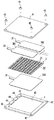
본 발명의 제1 실시 형태의 비선형 저항 소자(1)는 시트 형상으로 이루어진 세라믹 시트(2)와, 세라믹 시트(2)의 한 쌍의 주면(主面)의 각각에 분리가능한 상태로 배설된 복수의 전극판(301~303)과, 전극판(301~303)의 세라믹 시트(2)에 접촉하는 면과는 반대측의 면에 각각 배설된 한 쌍의 절연성 누름판(4)으로 구성되어 있다.The
세라믹 시트(2)는 산화 아연(ZnO)을 주성분으로 하는 세라믹 소결체로 구성된 복수의 세라믹 조각(또는 세라믹 비즈)(21)과, 이들의 세라믹 조각(21)의 각각을 이격된 상태에서 지지하는 절연성 소재로 구성된 지지 부재(22)로 구성되어 있다. 이것들의 세라믹 조각(21)은 절연성의 지지 부재(22)의 표면에서 노출되는 면과, 지지 부재(22)의 이면에서 노출되는 면을 가지고 있다. 또한, 이들의 세라믹 조각(21)은 서로 이격하여 배치된 상태에서 지지 부재(22)에 의해 지지되고 있으며, 이들 각각의 세라믹 조각(21)은 각각 독립된 비선형 저항 소자(바리스타, 또는 축전기 겸용 바리스타 등)로서 이용가능한 복수의 유닛 영역(23)을 형성하고 있다.The
또한, 제1 실시 형태에서는, 세라믹 조각(21)은 세라믹 시트(2)의 주면에 나란한 방향으로 각각을 이격시킨 상태로 지지되어 있지만, 동일한 유닛 영역(23)내라면, 각각 당접시켜도 좋다. 또한, 세라믹 조각(21)은 원형에 한정되는 것이 아니고, 장방형, 다각형 등 기타 각형, 타원형, 구형 또는 타원 구형 등이어도 좋다. In the first embodiment, the
또한, 세라믹 시트(2)는, 이하의 방법에 의하여 제작된다. 우선, 주성분인 ZnO에, Bi2O3:0.5mol%, Sb2O3:1.0mol%, Co2O3:0.5mol%, MnO2:0.5 mol%, Cr2O3:0.5mol%, Al(NO3)·9H2O:0.01mol%를 첨가하여 용제 및 분산제를 넣고 혼합한 뒤 결합재를 넣고 슬러리를 제작하는 스프레이 드라이어로 분체를 만든다. 그 분체를 금형에 성형해 지름 4.3 mm, 두께 1.2 mm의 성형체를 얻는다. 그 성형체를 1100℃에서 2시간 소성하고 두께 1 mm에서 직경 3.6mm의 원형 세라믹 조각(21)을 형성한다. 또한, 필요에 따라 세라믹 조각(21)을 열 처리한다.Further, the
이렇게 얻어진 복수의 세라믹 조각(21)을, 예를 들면, 금형 내에 서로 이격시켜 동일 평면상에 배열하여, 복수의 세라믹 조각(21)의 간격에 절연성 수지를 주입하는 사출 성형법 또는 삽입 성형법에 따라 세라믹 시트(2)를 제작한다.The plurality of
또한, 앞에서 사출 성형법 또는 삽입 성형법에 의한 세라믹 시트(2)가 제작된다고 설명하고 있지만, 세라믹 시트(2)의 제작 방법은 이에 한정되지 않는다. 예를 들면, 세라믹 조각(21)과 유동성이 있는 상태의 절연성 수지를 혼련하여 압출하는 방법(닥터 블레이드법이나 압출 성형법), 혹은, 세라믹 조각(21)과 열이나 자외선 등으로 경화하는 수지를 틀에 넣어 수지를 경화하는 방법에 의하여 세라믹 시트(2)를 제작해도 좋다.It is explained that the
또한, 세라믹 조각(21)의 재료 조성은 주성분인 산화 아연에 Bi2O3를 첨가한 Bi2O3계의 비선형 저항 소자(1)에 한하지 않고 Pr6O11계, BaTiO3계, SrTiO3계, TiO2계열, SnO2계 및 Fe3O4계의 비선형 저항 소자(1)라도 좋다. 또, 상기 실시 형태에서는, 세라믹 조각(21)이 산화 아연을 주성분으로 하는 소결체로 이루어진다고 설명하고 있지만, 예를 들면, 티타늄산 스트론튬, 탄화 규소, 산화 주석 등의 비선형성의 전기 저항 특성을 가진 세라믹이면 된다.The material composition of the
또, 세라믹 조각(21)을 접착하는 지지 부재(22)로서는, 난연성, 내열성이나 열 전도성이 뛰어난 수지 재료를 사용함으로써, 열적 성질의 향상이나 전기 성능 개선을 도모할 수 있다. 이 수지 재료 자체의 선택에만 국한되지 않고, 난연성, 내열성이나 열 전도성을 개선하기 위한 각종 첨가물을 첨가하는 것도 효과적이다. 예를 들면, 알루미나, 질화 알루미늄, 질화 붕소 등의 산화물, 비 산화물의 첨가나, 열 전도성 입자(금속 혹은 비금속 화합물을 불문하다)의 표면을 절연 가공한 입자, 경우에 따라서는 도전성 입자를 절연성이 저하하지 않는 범위에서 미량 첨가되어도 좋다. As the
전극판(301~303)은 구리, 황동과 알루미늄 등의 도전체로 구성된 금속제의 평탄한 판재로 구성되어, 배선 기판 등과 전기적으로 접속하기 위한 단자부(31)가 전극판(301~303)의 본체부로부터 일체적으로 연설되고 있다. 이 단자부(31)를 이용함으로써, 예를 들면, 비선형 저항 소자가 배선 기판 등에 실장이 용이하다.The
도 2에서 2점 쇄선으로 둘러싸인 영역은, 세라믹 시트(2)의 해당 상측의 주면에 배설된 전극판(301~303)을 나타내고 있다. 또한, 도 2에서 파선으로 둘러싸인 영역은 실시예 별로 달리 정의된 유닛 영역(23)을 나타내고 있다. 여기에서는 도 1에 제시된 세라믹 시트(2) 상측 주면에 있어서 유닛 영역(23)의 배치 형태만이 나타나 있다.In Fig. 2, the region enclosed by the chain double-dashed line shows the
9행 9열로 배치되는 세라믹 조각(21)이 각각 9차의 정방 행렬 요소{aij(i=1~9, j=1~9)}에 의해 구별되고 있다고 생각한다.It is assumed that the
도 2에 제시된 실시예에 의하면, 세라믹 시트(2) 상측 주면에는 2개의 전극판(301 및 302)이 배치되고, 하측 주면에는 1개의 전극판(303)이 배치된다. 해당 상측의 2개의 전극판(301 및 302)의 각각이 접하는 세라믹 조각(21)의 조합은 2개의 군(aij(i=1~9, j=1~4) 및 (aij(i=1~9, j=6~9)) 각각에 의해 나타난다.According to the embodiment shown in Fig. 2, two
즉, 이 경우, 세라믹 시트(2) 상측 주면에서는, 세라믹 조각(21)의 해당 2개의 군을 포함하는 2개의 유닛 영역(23)이 정의된다(도 2 파선 참조). 한편, 해당 하부의 전극판(303)은 모두 세라믹 조각(21)의 군(aij(i=1~9, j=1~9))이다.That is, in this case, on the upper main surface of the
전극판(301)→ 세라믹 조각(21)의 군(aij(i=1~9, j=1~4))→ 전극판(303)→ 세라믹 조각(21)의 군(aij(i=1~9, j=6~9))→ 전극판(302)이라는 일련의 전기 도통 경로를 구성하는 비선형 저항 소자(1)를 얻을 수 있다.The electrode plate (301) → the group of ceramic pieces (21) (a ij (i = 1 ~ 9, j = 1 ~ 4)) → the electrode plate (303) → the group of ceramic pieces (21) (a ij (i = 1 to 9, j = 6 to 9)) - > the
또한, 전극판(301 및 302)는 각각 해당하는 유닛 영역(23) 사이에 배치된 세라믹 조각(21)의 군(aij(i=1~9, j=5))이 포함되는 경계 영역(24)에 존재하는 절연성 소재에 따라 단락이 방지되고 있다. 이로써, 세라믹 시트(2) 상측 주면에 배설된 전극판(301 및 302)의 간격 t의 협소화를 꾀한다.Each of the
또한, 세라믹 시트(2)의 세라믹 조각(21)과 전극판(301~303)은 도전성 수지 (5)를 개재시켜 도전시켜도 좋다. 이에 따라 제조시에 각각의 세라믹 시트(2)의 표면과 이면에 다소 차이가 발생해도, 세라믹 조각(21)과 전극판(301~303)을 확실히 도전시킬 수 있다. The
도전성 수지(5)는 세라믹 조각(21) 또는 세라믹 시트(2)의 한쪽 혹은 양쪽의 면에 은 입자와 열 가소성 수지를 포함한 도전 페이스트를 도포 및 건조시켜 형성된다. 도전성 수지(5)의 재료 조성은 전도 입자로서 은을 포함하는 상온 경화형 도전성 접착제나 그 이외에 열 경화형의 도전성 접착제의 사용이 가능하다. 또한 전도 입자로서는 은 이외에도, 동이나 금 또는 탄소 등을 이용할 수 있다. The
누름판(4)은 세라믹 시트(2) 및 전극판(301~303) 보다 큰 표면적을 갖는 평판 모양으로 형성되어 있다. 또한, 누름판(4)의 네 모퉁이에는, 세라믹 시트(2) 및 전극판(301~303)이 누름판의 사이에 끼인 체결 상태와, 누름판에서 세라믹 시트 및 전극판이 분리된 분리 상태를 전환하기 위한 숫나사부(41)(선택 수단)를 가지고 있다. 이 숫나사부(41)는 누름판(4)의 한편에 형성된 암나사부(42)에 합쳐진다. 즉, 숫나사부(41)을 체결함으로써, 세라믹 시트(2) 및 전극판(301~303)이 누름판(4) 사이에 끼인 상태에서 고정된다. 그리고, 숫나사부(41)를 풀어줌으로써 누름판(4)에서 세라믹 시트(2) 및 전극판(301~303)이 각각 분리된다.The
이에 따라 비선형 저항 소자(1)의 전기적 특성을 변경하는 경우 또는 세라믹 시트(2)의 성능이 저하된 경우에도, 비선형 저항 소자 본체의 세라믹 시트(2) 또는 전극판(301~303)의 교환이 쉽게 이루어질 수 있으므로, 비선형 저항 소자의 보수성이 향상될 수 있다.Thus, even when the electrical characteristics of the
예를 들면, 피뢰기나 서지 흡수기의 사양 용도에 따라 바리스타 전압, 에너지 내성의 양 등의 전기적 특성의 변경이 요구되는 경우가 있다. 이런 경우, 기존의 전극판과 세라믹 소결체(세라믹 시트)가 납 땜된 비선형 저항 소자에서는 복수의 비선형 저항 소자를 제조하고, 이들을 직렬 또는 병렬로 접속하여 바리스타 전압, 에너지 내성의 양을 조절한다는 대책이 가능하다. 하지만 이런 대책은 새로운 복수의 비선형 저항 소자를 설치하는 공간을 확보하고, 경우에 따라서는 배선 기판의 설계 변경이 필요하기 때문에 비선형 저항 소자의 전기적 특성을 변경하는 것이 어려웠다. For example, it may be required to change the electrical characteristics such as the varistor voltage and the amount of energy resistance depending on the application of the lightning arrester or the surge absorber. In this case, in a non-linear resistance element in which a conventional electrode plate and a ceramic sintered body (ceramic sheet) are soldered, a plurality of non-linear resistance elements are manufactured and connected in series or in parallel to control the amount of varistor voltage and energy resistance It is possible. However, this countermeasure has made it difficult to change the electrical characteristics of the nonlinear resistive element because a space for installing a plurality of new nonlinear resistive elements is secured and, in some cases, the design of the wiring board is required to be changed.
이에 대해 본 발명에 관한 제1 실시 형태의 비선형 저항 소자(1)에 따르면 기존의 비선형 저항 소자처럼, 세라믹 시트(2) 및 전극판(301~303)이 납 땜 등에 의해 접합되지 않아 세라믹 시트(2)와 전극판(301~303)을 분리하여 바꾸는 것이 가능하다. 이 때문에, 비선형 저항 소자(1)의 전기적 특성을 쉽게 변경할 수 있다. On the other hand, according to the
각 전극판(301~303)과 해당 각 전극판(301~303)과 접합하는 세라믹 조각(21)이 포함되어 있는 각 유닛 영역(23)과 각각의 면적, 형상 및 배치 형태 중 적어도 1개가 변경됨으로써 복수의 세라믹 조각(21)을 구성 요소로 하는 단일의 세라믹 시트(2)에 의하여 복수의 다른 전기 특성을 갖는 비선형 저항 소자(1)가 구성될 수 있다.At least one of the area, shape, and arrangement of each
전기 특성이 다른 비선형 저항 소자(1)의 구성의 실시예에 대해 도 3을 참조하면서 설명한다. 도 3(a)~(c)의 각각의 오른쪽에서 파선으로 둘러싸인 영역은 실시예 별로 달리 정의된 유닛 영역(23)을 나타내고 있다. 여기에서 도 3(a)~(c)의 각각의 왼쪽에 보이는 세라믹 시트(2) 상측 주면에 있어서 유닛 영역(23)의 배치 형태만이 나타나 있다. 또 도 3(a)~(c)의 각각의 우측에서 두점 쇄선으로 둘러싸인 영역은, 세라믹 시트(2)의 해당 상측의 주면에 배설된 전극판(311~313, 321~324, 331~332)을 나타내고 있다.An embodiment of the configuration of the
9행 9열로 배치되는 세라믹 조각(21)의 각각이 9차의 정방 행렬 요소{aij(i=1~9, j=1~9)}에 의해 구별되고 있다고 생각한다.It is assumed that each of the
도 3(a) 좌측에 보이는 실시예에 의하면, 세라믹 시트(2) 상측 주면에는 3개의 전극판(311~313)이 배치되고, 하측의 주면에는 2개의 전극판(314 및 315)이 배치된다. 해당 상측의 3개의 전극판(311~313)의 각각이 접하는 세라믹 조각(21)의 조합은 3개의 군(aij(i=1~4, j=1~4), aij(i=1~4, j=6~9) 및 aij(i=6~9, j=1~9))의 각각에 의해 나타난다. 당해 하측 2개의 전극판(314 및 315)의 각각이 접하는 세라믹 조각(21)의 조합은 2개의 군(aij(i=1~9, j=1~4) 및 aij(i=1~9, j=6~9))의 각각이다.3 (a), three
즉, 이 경우, 세라믹 시트(2)의 상측 주면에서는, 세라믹 조각(21)의 해당 3개의 군을 포함하는 3개의 유닛 영역(23)이 정의된다(도 3(a) 파선 참조). 한편, 세라믹 시트(2) 하측의 주면에서는, 세라믹 조각(21)의 해당 2개의 군의 각각을 포함하는 2개의 유닛 영역(23)이 정의된다.That is, in this case, on the upper main surface of the
전기 극판(311)→ 세라믹 조각(21)의 군(aij(i=1~4, j=1~4))→ 전극판(314)→ 세라믹 조각(21)의 군(aij(i=6~9, j=1~4))→ 전극판(313)→ 세라믹 조각(21)의 군(aij(i=6~9, j=6~9))→ 전극판(315)→ 세라믹 조각(21)의 군(aij(i=1~4, j=6~9))→ 전극판(312)라는 일련의 전기 도통 경로를 구성하는 바리스타 전압이 큰 비선형 저항 소자(1)를 얻을 수 있다.Electrical plate (311) → the group of ceramic pieces (21) (a ij (i = 1 ~ 4, j = 1 ~ 4)) → the electrode plate (314) → the group of ceramic pieces (21) (a ij (i = 6 to 9, j = 1 to 4)) →
또한, 전극판(311 및 312)은 각각 해당하는 유닛 영역(23) 사이에 배치된 세라믹 조각(21)의 군(aij(i=1~4, j=5))이 포함되는 경계 영역(24)에 존재하는 절연성 소재에 따라 단락이 방지되고 있다. 전극판(311 및 313), (312 및 313) 및 (314 및 315) 역시 단락이 방지되고 있다. 이것으로 제1 실시 형태와 마찬가지로 해당 전극판의 간격 t의 협소화를 꾀한다.The
또한, 도 3(b) 좌측 실시예에 의하면, 세라믹 시트(2) 좌측의 주면에는 4개의 전극판(321~324)이 배치되어, 하측의 주면에는 2개의 전극판(325 및 326)이 배치된다. 해당 상측의 4개의 전극판(321~324)의 각각이 접하는 세라믹 조각(21)의 조합은 4개의 군(aij(i=1~4, j=1~4), aij(i=1~4, j=6~9), aij(i=6~9, j=1~4) 및 aij(i=6~9, j=6~9))의 각각에 의해 표시된다. 당해 하측 2개의 전극판(325 및 326)의 각각에 접하는 세라믹 조각(21)의 조합은 2개의 군(aij(i=1~4, j=1~9) 및 aij(i=6~9, j=1~9))의 각각이다.3 (b), four
즉, 이 경우, 세라믹 시트(2) 상측의 주면에서는, 세라믹 조각(21)의 해당 4개의 군을 포함하는 4개의 유닛 영역(23)이 정의된다(도 3(b) 파선 참조). 한편, 세라믹 시트(2) 하측의 주면에서는, 세라믹 조각(21)의 해당 2개의 군의 각각을 포함하는 2개의 유닛 영역(23)이 정의된다.That is, in this case, four
비선형 저항 소자(1)가 2개의 별개의 비선형 저항 소자로서 구성된다. 즉, 전극판(321)→ 세라믹 조각(21)의 군(aij(i=1~4, j=1~4))→ 전극판(325)→ 세라믹 조각(21)의 군(aij(i=1~4, j=6~9))→ 전극판(322) 이라는 일련의 전기 도통 경로와, 전극판(323)→ 세라믹 조각(21)의 군(aij(i=6~9, j=1~4))→ 전극판(326)→ 세라믹 조각(21)의 군(aij(i=6~9, j=6~9))→ 전극판(324)라는 일련의 전기 도통 경로의 각각에 의해 구성되는 2개의 비선형 저항 소자가 구성된다.The
또한, 전극판(321 및 322)는 각각 해당하는 유닛 영역(23) 사이에 배치된 세라믹 조각(21)의 군(aij(i=1~4, j=5))이 포함되는 경계 영역(24)에 존재하는 절연성 소재에 따라 단락이 방지되고 있다. 전극판(321 및 323), (322 및 324), (323 및 324) 및 (325 및 326) 역시 단락이 방지되고 있다. 이것으로 제1 실시 형태와 마찬가지로 해당 전극판의 간격 t의 협소화를 꾀한다.The
또한, 도 3(c) 좌측 실시예에 의하면, 세라믹 시트(2) 상측 주면에는 2개의 전극판(331 및 332)이 배치되어, 하측 주면에는 2개의 전극판(333 및 334)이 배치된다. 해당 상측의 2개의 전극판(331 및 332)의 각각이 접하는 세라믹 조각(21)의 조합은 2개의 군(aij(i=1~9, j=1~4) 및 aij(i=1~9, j=6~9))의 각각으로 표시된다. 당해 하측 2개의 전극판(333 및 334)의 각각이 접하는 세라믹 조각(21)의 조합은 2개의 군(aij(i=1~9, j=1~4) 및 aij(i=1~9, j=6~9))의 각각이다.3 (c), two
즉, 이 경우, 세라믹 시트(2) 상측 주면에서는, 세라믹 조각(21)의 해당 2개의 군을 포함하는 2개의 유닛 영역(23)이 정의된다(도 3(c) 파선 참조). 한편, 세라믹 시트(2) 하측 주면에서는, 세라믹 조각(21)의 해당 2개의 군의 각각을 포함하는 2개의 유닛 영역(23)이 정의된다.That is, in this case, two
비선형 저항 소자(1)가 2개의 별개의 비선형 저항 소자로서 구성된다. 즉, 전극판(331)→ 세라믹 조각(21)의 군(aij(i=1~9, j=1~4))→ 전극판(333)라는 일련의 전기 도통 경로와, 전극판(332)→ 세라믹 조각(21)의 군(aij(i=6~9, j=1~4))→ 전극 판(334)라는 일련의 전기 도통 경로의 각각에 의해 구성되는 2개의 비선형 저항 소자가 구성된다.The
또한, 전극 판자(331 및 332)는 각각 해당 유닛 영역(23) 사이에 배치된 세라믹 조각(21)의 군(aij(i=1~9, j=5))이 포함되는 경계 영역(24)에 존재하는 절연성 소재에 따라 단락이 방지되고 있다. 전극판(333 및 334)도 마찬가지로 단락이 방지되고 있다. 이것으로 제1 실시 형태와 마찬가지로 해당 전극판의 간격 t의 협소화를 꾀한다.In addition, the electrode board (331 and 332) are each the
또한, 누름판(4)에는, 세라믹 시트(2) 및 전극판(301~303)의 본체부가 끼어들어가는 수용부(43)와 전극판(301~303)의 단자부(31)가 누름판(4)의 바깥쪽으로 안내되는 안내 홈(44)이 형성되어 있다. 이로써, 세라믹 시트(2) 및 전극판(301~303)을 누름판(4) 사이에 끼는 경우에, 세라믹 시트(2) 및 전극판(301~303)이 소정의 위치에 배치됨으로써 비선형 저항 소자(1)의 조립 작업이 쉽게 된다.The
또 누름판(4)은 아크릴 수지 등의 투명 부재로 구성되는 것이 바람직하다. 이에 따라 비선형 저항 소자(1)를 분해하지 않고 조립된 상태에서 사용 중인 세라믹 시트(2) 및 전극판(301~303)의 크기, 형상 등을 확인할 수 있다.The
또한, 세라믹 시트(2) 및 전극판(301~303)의 체결 상태와 분리 상태를 전환하는 선택 수단은 숫나사부(41) 및 암나사부(42)에 한정되지 않는다. 예를 들어, 누름판(4)의 양끝에 클립 같은 것으로 끼어서, 세라믹 시트(2) 및 전극판(301~303)의 체결 상태를 고정해도 좋다. 또 이른바 스냅 피트처럼 한쪽 누름판에 손톱부를 만들어 재료의 탄성을 이용하고 다른 쪽에 누름판을 걸치고 고정해도 좋다.
The selecting means for switching the fastening state and the separated state of the
(본 발명의 다른 실시 형태)(Another embodiment of the present invention)
다음으로, 본 발명에 관한 비선형 저항 소자의 제2 내지 제5 실시 형태에 대해 도 4 내지 7을 참조하면서, 이하에 기술한다.Next, the second to fifth embodiments of the non-linear resistance element according to the present invention will be described below with reference to Figs. 4 to 7. Fig.
덧붙여 도 1 및 2에 나타낸 구성에 대해서는 동일한 부호를 붙여 설명을 생략한다. 제2 내지 제5 실시 형태의 비선형 저항 소자(1)는 상기 제1 실시 형태의 유닛 영역(23)에 배치된 세라믹 조각(21)의 구성만 상이하다. 1 and 2 are denoted by the same reference numerals, and a description thereof will be omitted. The
본 발명의 제2 실시 형태의 세라믹 조각(21)은 도 4와 같이 원주형으로 되어, 절연성의 지지 부재(22)의 표면으로부터 노출하는 면(211)과 지지 부재(22)의 이면에서 노출하는 면(212)을 가지고 있다. 그리고, 유닛 영역(23)에는 하나의 유닛 영역(23)에 대한 복수의 세라믹 조각(21)으로 구성되며, 이들의 세라믹 조각(21)이 서로 도전 가능하게 접하고 있다.The
본 발명의 제3 실시 형태의 세라믹 조각(21)은 도 5와 같이 평면 모양으로 형성되어, 절연성의 지지 부재(22)의 표면으로부터 노출하는 면(211)과 지지 부재 (22)의 이면에서 노출하는 면(212)을 가지고 있다. 그리고, 유닛 영역(23)에는 하나의 유닛 영역(23)에 대한 하나의 세라믹 조각(21)으로 구성되며, 유닛 영역(23)은 두곳으로만 구성된다. The
본 발명의 제4 실시 형태의 세라믹 조각(21)은 도 6과 같이 구형으로 형성되고, 세라믹 시트(2)의 수평 방향 및 두께 방향으로 각각 서로 당접하는 복수의 세라믹 조각 군(213)을 구성하고 있다. 이들의 세라믹 조각 군(213)은, 세라믹 시트의 두께 방향으로 관통하는 복수의 도통 경로를 각각 구성하고, 이들의 도통 경로는 지지 부재(22)의 표면부터 부분적으로 돌출하는 면(211)과 지지 부재(22)의 이면에서 부분적으로 돌출하는 면(212)를 가지고 있다. 그리고, 유닛 영역(23)에는 하나의 유닛 영역(23)에 대한 복수의 세라믹 조각 군(213)으로 이루어지며, 세라믹 시트(2)의 동일 평면상에 절연성의 지지 부재(22)를 통해 서로 이격되어 배열되어 있다.The
본 발명의 제5 실시 형태의 세라믹 조각(21)은 도 7과 같이 구형으로 형성되어, 절연성의 지지 부재(22)의 표면에서 돌출하는 면(211)과 지지 부재(22)의 이면에서 돌출하는 면(212)을 가지고 있다. 그리고, 유닛 영역(23)에는 하나의 유닛 영역(23)에 대한 복수의 세라믹 조각(21)으로 구성되며, 세라믹 시트(2)의 동일 평면상에 절연성의 지지 부재(22)를 통해 서로 이격되어 배열되어 있다.The
또한, 본 발명의 제5 실시 형태의 지지 부재(22)는 난연성, 내열성이나 열 전도성에 더해 탄성적으로 휘어지는 가요성이 뛰어난 절연성 수지로 구성되어 있다. 예를 들면, 우레탄계 엘라스토머나 올레인계 엘라스토머 등의 합성 수지로 된 것이 바람직하다.In addition, the
이를 통해 본 발명의 제5 실시 형태의 세라믹 시트(2)는 지지 부재(22)의 탄성력에 의해 휘어질 수 있으므로 도 7에서 나타내듯이 전극판(301~303)이 크게 만곡하게 형성되어 있어도 이 전극판(301~303)의 표면에 맞게 변형시켜, 세라믹 조각 (21)의 돌출 부분을 해당 전극판(301~303)에 대해 확실히 당접시킬 수 있다.The
이들 도 5 내지 도 7에 제시된 제2 내지 제5 실시 형태는 어느 것도 유닛 영역(23)이 절연성의 지지 부재(22)로 구성된 경계 영역(24)에 따라 구분된다. 이 때문에, 복수의 전극판(301~303)이 복수의 유닛 영역(23)의 배치 유형에 따라 동일 평면상에 배설된 경우 이들의 전극판(301~303)의 단락이 방지되고 제1 실시 형태와 마찬가지로 이들의 전극판(301~303)의 간격 t의 협소화를 꾀한다. 5 to 7, the
또한, 이들 도 5 내지 도 7에 제시된 제2 내지 제5 실시 형태는 제1 실시 형태와 마찬가지로 누름판(4)에 따라, 세라믹 시트(2)와 전극판(301~303)을 분리하여 떼어내는 것이 가능하다. In the second to fifth embodiments shown in Figs. 5 to 7, the
이에 따라 비선형 저항 소자(1)의 전기적 특성을 변경하는 경우 또는 세라믹 시트(2)의 성능이 저하된 경우라도, 비선형 저항 소자 본체의 세라믹 시트(2) 또는 전극판(301~303)의 교환을 쉽게 할 수 있다. 예를 들면, 세라믹 시트(2)가 고장난 경우 새로운 세라믹 시트(2)를 바꿔도 좋고, 다른 실시 형태와 형태가 다른 세라믹스 시트(2)로 바꿔도 좋다. 또한, 종래처럼 일체적으로 연소된 세라믹 소결체로 구성된 세라믹 시트(2)로 바꿔도 좋고, 이러한 경우도, 도 8에 나타난 제6 실시 형태처럼, 전극판(301~3031) 단자와 다단자의 교환 등을 쉽게 할 수 있으므로, 비선형 저항 소자(1)의 변경 및 조립이 쉽게 가능하다는 본 발명의 효과를 얻을 수 있다.Thus, even when the electrical characteristics of the
이상, 본 발명의 실시 형태에 대해서 도면을 참조해 설명하였으나, 본 발명은 이에 한정되지 않는다. 예를 들어, 도 1 내지 도 7에 나타내는 상기 제1 내지 제5의 실시 형태에서는, 세라믹 조각(21)이 규칙적으로 배치되어 있지만, 불규칙적으로 배치되어 있어도 좋다. 세라믹 시트(2)의 형상은 직사각형 모양뿐만 아니라 원형 모양 등 그 용도에 맞추어 임의로 변경될 수 있다
While the embodiments of the present invention have been described with reference to the drawings, the present invention is not limited thereto. For example, in the first to fifth embodiments shown in Figs. 1 to 7, the
1...비선형 저항 소자
2...세라믹 시트
21...세라믹 조각
23...유닛 영역
24...경계 영역
301~303...전극판
4...누름판1 ... nonlinear resistance element
2 ... ceramic sheet
21 ... ceramic sculpture
23 ... unit area
24 ... boundary region
301 ~ 303 ... electrode plate
4 ... pressing plate
Claims (3)
하나 또는 복수의 상기 세라믹 조각이 상기 세라믹 시트를 그 두께방향으로 관통하는 복수의 도통 경로의 각각을 구성하며,
또한 상기 도통 경로의 양단을 구성하는 상기 세라믹 조각이 상기 지지부재로부터 부분적으로 노출되어 있는 비선형 저항 소자로서,
복수의 상기 세라믹 조각이 서로 이격하여 있는 복수의 유닛 영역의 각각에 구분되어 배치되어 있는 상태로, 복수의 상기 세라믹 조각의 각각이 상기 지지부재에 의하여 지지되고 있는 것을 특징으로 하는 비선형 저항 소자.At least a ceramic sheet composed of a plurality of ceramic pieces composed of a ceramic sintered body and a sheet-like support member made of an insulating material for supporting each of the plurality of ceramic pieces,
One or a plurality of said ceramic pieces constituting each of a plurality of conductive paths passing through said ceramic sheet in its thickness direction,
And the ceramic piece constituting both ends of the conduction path is partially exposed from the supporting member,
Wherein each of the plurality of ceramic pieces is supported by the support member in a state in which a plurality of the ceramic pieces are separately arranged in each of a plurality of unit regions spaced apart from each other.
상기 세라믹 시트의 한 쌍의 주면(主面) 중 일방 또는 양방에 있어서, 복수의 상기 유닛 영역의 각각에 배치되어 있는 단일 또는 복수의 상기 세라믹 조각과 전기적으로 도통하고, 또한, 상기 지지부재 중 상이한 상기 유닛 영역 간의 경계영역을 끼고 서로 이격하여 있는 상태로 배설된 복수의 전극판을 구비하고 있는 것을 특징으로 하는 비선형 저항 소자.The method according to claim 1,
Wherein one or both of the pair of main surfaces of the ceramic sheet are electrically connected to one or a plurality of the ceramic pieces arranged in each of the plurality of unit areas, And a plurality of electrode plates arranged so as to be spaced apart from each other with a boundary region between the unit regions.
상기 세라믹 시트의 한 쌍의 주면의 각각에 상기 전극판이 배설되어 있는 것에 있어서,
상기 전극판의 상기 세라믹 시트에 접촉하는 면과는 반대측의 면에 각각 배설되는 한 쌍의 절연성의 누름판과
복수의 상기 전극판이 각각 대응하는 복수의 상기 유닛 영역에 배치된 세라믹 조각과 전기적으로 도통하고,
또한 상기 세라믹 시트와 그 한 쌍의 주면의 각각에 당접하는 한 쌍의 상기 전극판과 상기 누름판의 사이에 끼어 있는 체결 상태와, 상기 누름판에서 상기 세라믹 시트와 그 한 쌍의 주면의 각각에 당접하는 한 쌍의 상기 전극판이 분리하는 분리 상태를 전환하는 선택수단을 구비하는 것을 특징으로 하는 비선형 저항 소자.3. The method of claim 2,
Wherein the electrode plate is disposed on each of a pair of main surfaces of the ceramic sheet,
A pair of insulating pressure plates arranged on surfaces of the electrode plates opposite to the surfaces contacting the ceramic sheets,
A plurality of said electrode plates are electrically connected to ceramic pieces arranged in a corresponding plurality of said unit areas,
A pressing state in which the ceramic sheet is sandwiched between a pair of the electrode plates and the pressing plate which are in contact with the ceramic sheet and a pair of main surfaces of the ceramic sheet and a pressing state in which the pressing sheet is in contact with each of the ceramic sheet and the pair of main surfaces thereof And a selection means for switching a separation state in which a pair of the electrode plates are separated from each other.
Applications Claiming Priority (3)
| Application Number | Priority Date | Filing Date | Title |
|---|---|---|---|
| JP2012085966A JP5998329B2 (en) | 2012-04-04 | 2012-04-04 | Nonlinear resistance element |
| JPJP-P-2012-085966 | 2012-04-04 | ||
| PCT/JP2013/059245 WO2013150953A1 (en) | 2012-04-04 | 2013-03-28 | Nonlinear resistive element |
Publications (1)
| Publication Number | Publication Date |
|---|---|
| KR20140140475A true KR20140140475A (en) | 2014-12-09 |
Family
ID=49300443
Family Applications (1)
| Application Number | Title | Priority Date | Filing Date |
|---|---|---|---|
| KR1020137031796A KR20140140475A (en) | 2012-04-04 | 2013-03-28 | Nonlinear resistive element |
Country Status (6)
| Country | Link |
|---|---|
| US (1) | US8902039B2 (en) |
| EP (1) | EP2704158B1 (en) |
| JP (1) | JP5998329B2 (en) |
| KR (1) | KR20140140475A (en) |
| CN (1) | CN103563014B (en) |
| WO (1) | WO2013150953A1 (en) |
Families Citing this family (11)
| Publication number | Priority date | Publication date | Assignee | Title |
|---|---|---|---|---|
| JP5998328B2 (en) | 2012-04-04 | 2016-09-28 | 音羽電機工業株式会社 | Nonlinear resistance element |
| TWI600354B (en) * | 2014-09-03 | 2017-09-21 | 光頡科技股份有限公司 | Micro-resistance structure with high bending strength, manufacturing method thereof |
| US10083781B2 (en) | 2015-10-30 | 2018-09-25 | Vishay Dale Electronics, Llc | Surface mount resistors and methods of manufacturing same |
| CN105469915A (en) * | 2015-11-05 | 2016-04-06 | 隆科电子(惠阳)有限公司 | Metal oxide varistors (MOV) component structure fixed by fastening element |
| WO2017075842A1 (en) * | 2015-11-05 | 2017-05-11 | 隆科电子(惠阳)有限公司 | Mov device structure fixed by means of a fastener |
| CN105304243A (en) * | 2015-11-12 | 2016-02-03 | 郑品章 | Voltage dependent resistor (VDR) |
| CN106782957B (en) * | 2017-01-17 | 2019-05-17 | 隆科电子(惠阳)有限公司 | A kind of compound MOV component with discharging structure |
| US10438729B2 (en) | 2017-11-10 | 2019-10-08 | Vishay Dale Electronics, Llc | Resistor with upper surface heat dissipation |
| KR102139772B1 (en) * | 2018-11-27 | 2020-07-31 | 삼성전기주식회사 | Varistor and varistor manufacturing method |
| US11545284B2 (en) * | 2019-01-16 | 2023-01-03 | Panasonic Intellectual Property Management Co., Ltd. | Varistor assembly |
| TWI687944B (en) * | 2019-08-15 | 2020-03-11 | 聚鼎科技股份有限公司 | Positive temperature coefficient device |
Family Cites Families (14)
| Publication number | Priority date | Publication date | Assignee | Title |
|---|---|---|---|---|
| GB1037822A (en) * | 1961-12-15 | 1966-08-03 | Ass Elect Ind | Improvements relating to non-linear electrical resistance elements |
| NL6901659A (en) * | 1969-02-01 | 1970-08-04 | ||
| US3648002A (en) | 1970-05-04 | 1972-03-07 | Essex International Inc | Current control apparatus and methods of manufacture |
| JPS60211801A (en) * | 1984-04-05 | 1985-10-24 | 松下電器産業株式会社 | Varistor |
| JPH0262005A (en) * | 1988-08-29 | 1990-03-01 | Matsushita Electric Ind Co Ltd | Sheet-shaped varistor |
| US5262754A (en) * | 1992-09-23 | 1993-11-16 | Electromer Corporation | Overvoltage protection element |
| US6055147A (en) * | 1998-06-24 | 2000-04-25 | Current Technology, Inc. | Apparatus for providing independent over-current protection to a plurality of electrical devices and transient-voltage suppression system employing the apparatus |
| US6323751B1 (en) * | 1999-11-19 | 2001-11-27 | General Electric Company | Current limiter device with an electrically conductive composite material and method of manufacturing |
| TW543258B (en) * | 2001-10-08 | 2003-07-21 | Polytronics Technology Corp | Over current protection apparatus and its manufacturing method |
| JP2004006519A (en) | 2002-05-31 | 2004-01-08 | Otowa Denki Kogyo Kk | Multi-terminal varistor |
| DE102006033710B4 (en) * | 2006-07-20 | 2013-04-11 | Epcos Ag | Method for producing a resistor arrangement |
| JP5150111B2 (en) * | 2007-03-05 | 2013-02-20 | 株式会社東芝 | ZnO varistor powder |
| DE102007030653B4 (en) * | 2007-07-02 | 2017-04-13 | Phoenix Contact Gmbh & Co. Kg | Snubber |
| EP2618342B1 (en) * | 2010-10-05 | 2016-01-13 | Otowa Electric Co., Ltd. | Non-linear resistive element and manufacturing method thereof |
-
2012
- 2012-04-04 JP JP2012085966A patent/JP5998329B2/en active Active
-
2013
- 2013-03-28 KR KR1020137031796A patent/KR20140140475A/en not_active Application Discontinuation
- 2013-03-28 CN CN201380001516.1A patent/CN103563014B/en active Active
- 2013-03-28 US US14/119,989 patent/US8902039B2/en active Active
- 2013-03-28 WO PCT/JP2013/059245 patent/WO2013150953A1/en active Application Filing
- 2013-03-28 EP EP13772928.1A patent/EP2704158B1/en active Active
Also Published As
| Publication number | Publication date |
|---|---|
| US20140085043A1 (en) | 2014-03-27 |
| EP2704158B1 (en) | 2016-05-25 |
| CN103563014B (en) | 2017-09-01 |
| JP2013219092A (en) | 2013-10-24 |
| EP2704158A1 (en) | 2014-03-05 |
| US8902039B2 (en) | 2014-12-02 |
| EP2704158A4 (en) | 2014-10-22 |
| CN103563014A (en) | 2014-02-05 |
| JP5998329B2 (en) | 2016-09-28 |
| WO2013150953A1 (en) | 2013-10-10 |
Similar Documents
| Publication | Publication Date | Title |
|---|---|---|
| KR20140140475A (en) | Nonlinear resistive element | |
| JP5640249B2 (en) | Nonlinear resistance element and manufacturing method thereof | |
| KR20170076636A (en) | Circuit protection device | |
| KR20200118833A (en) | Cascade varistors with improved energy handling capacity | |
| US20120144634A1 (en) | Metal oxide varistor design and assembly | |
| JP2004006519A (en) | Multi-terminal varistor | |
| EP2903158B1 (en) | Stacked chip device | |
| EP2709116B1 (en) | Nonlinear resistive element | |
| US4161763A (en) | Compact voltage surge arrester device | |
| US1734208A (en) | Lightning-arrester unit | |
| JP2007305934A (en) | Surge protection device | |
| CN203480967U (en) | Laminated PTC (positive temperature coefficient) thermistor | |
| KR100340130B1 (en) | Complex device of PTC thermistor-varistor and fabricating method therefor | |
| KR101282912B1 (en) | Varistor apparatus | |
| JP2011258490A (en) | Overvoltage protection component and method of manufacturing the same | |
| JPH02260605A (en) | Lamination type varistor | |
| WO2015087573A1 (en) | Compound electronic component | |
| JP2004040030A (en) | Voltage nonlinear resistor element | |
| JP2007165526A (en) | Chip-type positive characteristic thermistor |
Legal Events
| Date | Code | Title | Description |
|---|---|---|---|
| WITN | Application deemed withdrawn, e.g. because no request for examination was filed or no examination fee was paid |