KR20140100526A - Stacked chipset having an insulating layer and a secondary layer and method of forming same - Google Patents
Stacked chipset having an insulating layer and a secondary layer and method of forming same Download PDFInfo
- Publication number
- KR20140100526A KR20140100526A KR1020147016198A KR20147016198A KR20140100526A KR 20140100526 A KR20140100526 A KR 20140100526A KR 1020147016198 A KR1020147016198 A KR 1020147016198A KR 20147016198 A KR20147016198 A KR 20147016198A KR 20140100526 A KR20140100526 A KR 20140100526A
- Authority
- KR
- South Korea
- Prior art keywords
- chipset
- layer
- insulating layer
- circuit
- silicon substrate
- Prior art date
Links
Images

Classifications
-
- H—ELECTRICITY
- H01—ELECTRIC ELEMENTS
- H01L—SEMICONDUCTOR DEVICES NOT COVERED BY CLASS H10
- H01L27/00—Devices consisting of a plurality of semiconductor or other solid-state components formed in or on a common substrate
- H01L27/02—Devices consisting of a plurality of semiconductor or other solid-state components formed in or on a common substrate including semiconductor components specially adapted for rectifying, oscillating, amplifying or switching and having at least one potential-jump barrier or surface barrier; including integrated passive circuit elements with at least one potential-jump barrier or surface barrier
- H01L27/04—Devices consisting of a plurality of semiconductor or other solid-state components formed in or on a common substrate including semiconductor components specially adapted for rectifying, oscillating, amplifying or switching and having at least one potential-jump barrier or surface barrier; including integrated passive circuit elements with at least one potential-jump barrier or surface barrier the substrate being a semiconductor body
- H01L27/06—Devices consisting of a plurality of semiconductor or other solid-state components formed in or on a common substrate including semiconductor components specially adapted for rectifying, oscillating, amplifying or switching and having at least one potential-jump barrier or surface barrier; including integrated passive circuit elements with at least one potential-jump barrier or surface barrier the substrate being a semiconductor body including a plurality of individual components in a non-repetitive configuration
- H01L27/0688—Integrated circuits having a three-dimensional layout
-
- H—ELECTRICITY
- H01—ELECTRIC ELEMENTS
- H01L—SEMICONDUCTOR DEVICES NOT COVERED BY CLASS H10
- H01L2224/00—Indexing scheme for arrangements for connecting or disconnecting semiconductor or solid-state bodies and methods related thereto as covered by H01L24/00
- H01L2224/01—Means for bonding being attached to, or being formed on, the surface to be connected, e.g. chip-to-package, die-attach, "first-level" interconnects; Manufacturing methods related thereto
- H01L2224/18—High density interconnect [HDI] connectors; Manufacturing methods related thereto
Abstract
칩셋(100)은 유리, 석영 또는 사파이어의 시트(102) 및 제 1 기판층(106)의 제 1 측면(108) 상의 적어도 하나의 제 1 회로층(112)을 갖는 제 1 웨이퍼(104)를 포함한다. 제 1 웨이퍼(104)는 적어도 하나의 제 1 회로층(112)이 제 1 기판층(106)과 시트(102) 사이에 위치되도록 시트(102)에 접속된다. 제 2 기판층(120)의 제 1 측면(122) 상의 적어도 하나의 제 2 회로층(126)을 갖는 제 2 웨이퍼(126)는 적어도 하나의 제 2 회로층(126)이 제 2 기판층(120)과 제 1 기판층(106) 사이에 위치되도록 제 1 기판층(106)에 접속된다. 칩셋을 형성하는 방법이 또한 개시된다. The chipset 100 includes a first wafer 104 having a sheet 102 of glass, quartz or sapphire and at least one first circuit layer 112 on the first side 108 of the first substrate layer 106 . The first wafer 104 is connected to the seat 102 such that at least one first circuit layer 112 is positioned between the first substrate layer 106 and the sheet 102. The second wafer 126 having at least one second circuit layer 126 on the first side 122 of the second substrate layer 120 may be formed such that at least one second circuit layer 126 is formed on the second substrate layer 120 and the first substrate layer 106. The first substrate layer 106 is formed of a first substrate layer 106 and a second substrate layer 106, A method of forming a chipset is also disclosed.
Description
본 특허 출원은 2011년 11월 16일자로 출원되고 본원의 양수인에게 양도되고 그로 인해 본원에 인용에 의해 명백히 포함되는 "STACKED CMOS CHIPSET HAVING AN INSULATING LAYER AND A SECONDARY LAYER AND METHOD OF FORMING SAME"란 명칭의 미국 가출원 제 61/560,471 호를 우선권으로 주장한다. This patent application is a continuation-in-part of U.S. Patent Application Serial No. 10 / 711,501, entitled " STACKED CMOS CHIPSET HAVING AN INSULATING LAYER AND A SECONDARY LAYER AND METHOD OF FORMING SAME " filed November 16, 2011, assigned to the assignee hereof and expressly incorporated herein by reference. U.S. Provisional Application No. 61 / 560,471 as priority.
본 특허 출원은 절연체에 결합된 CMOS(complementary metal oxide semiconductor) 층 및 CMOS 층 상에 적층된 제 2 층을 갖는 칩셋 및 이를 형성하는 방법에 관한 것이며, 더 상세하게는, 절연체에 결합된 CMOS 층 및 패시브(passive) 엘리먼트들, 라디오 주파수(RF) 회로 또는 MEMS(microelectromechanical system) 엘리먼트들을 갖는 제 2 층을 포함하는 칩셋 및 이를 형성하는 방법에 관한 것이다. The present patent application relates to a CMOS (complementary metal oxide semiconductor) layer coupled to an insulator and a second layer having a second layer stacked on the CMOS layer and a method of forming the same, and more particularly to a CMOS layer and / A second layer having passive elements, radio frequency (RF) circuits or microelectromechanical system (MEMS) elements, and a method of forming the same.
셀룰러 무선 시스템들이 2G로부터 4G로 발달함에 따라, 더 많은 수들의 대역들을 지원하기 위한 라디오 주파수(RF) 칩셋들에 대한 증가하는 수요가 존재한다. 이러한 부가적인 대역들을 처리하는 능력을 칩셋들에 제공하는 것은 부가적인 트랜시버들, 필터들, 전력 증폭기들, 패시브 컴포넌트들 및 스위치들을 칩셋 프론트 엔드에 부가하는 것을 요구할 수 있고, 이것은 칩셋들의 비용 및 복잡성을 증가시킨다. 셀폰의 RF 시스템은 주로 2 개의 부분들: 종종 단일 CMOS(complementary metal oxide semiconductor) 칩인 트랜시버, 및 RF 프론트-엔드(다양한 온-보드 컴포넌트들: 필터들, 듀플렉서들, RF 스위치들, 전력 증폭기들 및 패시브들을 포함함)로 구성된다. CMOS 트랜시버가 상이한 대역들 또는 모드들에 의해 공유되도록 설계될 수 있지만(일반적으로 다중-모드/다중-대역 트랜시버 설계로 불림), 프론트-엔드 부분, 특히 필터들 및 듀플렉서들은 상이한 대역들 사이에서 공유될 수 없는데, 왜냐하면 간단히 그들이 상이한 주파수 대역에서 동작하기 때문이다. 더 많은 대역들/모드들을 지원하기 위한 이러한 부가적인 엘리먼트들의 존재는, 성능을 증가시키고 크기 및 비용을 감소시키려고 시도할 때, 프론트 엔드에 제한 요인이 되게 할 수 있다. As cellular wireless systems evolve from 2G to 4G, there is an increasing demand for radio frequency (RF) chipsets to support a greater number of bands. Providing chipsets with the ability to handle these additional bands may require adding additional transceivers, filters, power amplifiers, passive components, and switches to the chipset front end, which may reduce the cost and complexity of the chipsets . The cell phone's RF system consists mainly of two parts: a transceiver, often a single complementary metal oxide semiconductor chip, and an RF front-end (various on-board components: filters, duplexers, RF switches, power amplifiers, Passives). Although the CMOS transceiver may be designed to be shared by different bands or modes (commonly referred to as a multi-mode / multi-band transceiver design), the front-end portion, particularly the filters and duplexers, Because they simply operate in different frequency bands. The presence of these additional elements to support more bands / modes may cause the front end to be a limiting factor when attempting to increase performance and reduce size and cost.
종래의 다중-대역 및/또는 다중-모드 RF 칩셋 프론트 엔드들은 RF 스위치들, 전력 증폭기들, 음향 필터들 및 패시브들, 예를 들면, 인덕터들 및 커패시터들과 같은 디바이스들을 포함할 수 있다. CMOS 칩 엘리먼트들이 일반적으로 계속해서 스케일링할 수 있어서 새로운 기술적 진보들을 통해 더 낮은 비용 및 더 작은 크기를 발생시킬 수 있지만, 프론트 엔드는 항상 그와 같이 용이하게 스케일링되지는 않는다. 이러한 상황에 대한 하나의 접근법은 다수의 칩들, 예를 들면, GaAs 안테나 스위치들, GaAs 전력 증폭기들, CMOS 제어기들, SAW(surface acoustic wave) 필터들, 집적 패시브 디바이스들 등을 단일 래미네이트(laminate) 또는 세라믹 기판 상에 통합하는 것이다. 이러한 접근법은 프론트-엔드 통합에 대한 "시스템-인-패키지" 해결책으로 지칭될 수 있다. 튜닝 가능한 프론트 엔드를 도입함으로써 시스템 아키텍처 레벨에서 다중-대역 복잡성 문제를 해결하는데 또한 관심이 있다. 저손실 다중-대역 튜닝 가능한 시스템을 실현하기 위해, 반도체 버랙터들(varactors) 및 MEMS-기반 튜닝 가능한 커패시터들과 같은 하이-Q 튜닝 가능한 패시브들, 및 고성능 RF 스위치들을 단일 배열로 구현하는 방법이 발견되어야 한다. 프론트 엔드 통합은 또한 다중대역 및/또는 다중-모드 RF 트랜시버 칩셋들의 전체 크기 및 비용을 감소시키는데 유용할 수 있다. 따라서, CMOS 컴포넌트들과 다른 프론트 엔드 컴포넌트들을 공간- 및 비용-효율적인 방식으로 통합하는 칩셋을 제공하는 것이 바람직할 것이다. Conventional multi-band and / or multi-mode RF chipset front ends may include devices such as RF switches, power amplifiers, acoustic filters and passives, for example, inductors and capacitors. Although the CMOS chip elements are generally able to scale continuously, new technological advances can result in lower cost and smaller size, but the front end is not always so easily scaled. One approach to this situation is to use multiple laminates, such as GaAs antenna switches, GaAs power amplifiers, CMOS controllers, surface acoustic wave (SAW) filters, integrated passive devices, ) Or on a ceramic substrate. This approach may be referred to as a "system-in-package" solution to front-end integration. There is also interest in solving multi-band complexity problems at the system architecture level by introducing a tunable front end. In order to realize a low loss multi-band tunable system, it is necessary to find a way to implement high-Q tunable passives, such as semiconductor varactors and MEMS-based tunable capacitors, and high performance RF switches in a single arrangement do. Front-end integration may also be useful in reducing the overall size and cost of multi-band and / or multi-mode RF transceiver chipsets. Accordingly, it would be desirable to provide a chipset that integrates CMOS components and other front end components in a space-and cost-effective manner.
예시적인 실시예는 유리, 석영 또는 사파이어의 시트, 및 제 1 기판층의 제 1 측면 상에 적어도 하나의 제 1 회로층을 갖는 제 1 웨이퍼를 포함하는 칩셋을 포함한다. 제 1 웨이퍼는, 적어도 하나의 제 1 회로층이 제 1 기판층과 시트 사이에 위치되도록 시트에 접속된다. 칩셋은 또한 제 2 기판층의 제 1 측면 상에 적어도 하나의 제 2 회로층을 갖는 제 2 웨이퍼를 포함하고, 제 2 웨이퍼는 적어도 하나의 제 2 회로층이 제 2 기판층과 제 1 기판층 사이에 위치되도록 제 1 기판층에 접속된다. An exemplary embodiment includes a chipset comprising a sheet of glass, quartz or sapphire, and a first wafer having at least one first circuit layer on a first side of the first substrate layer. The first wafer is connected to the sheet such that at least one first circuit layer is positioned between the first substrate layer and the sheet. The chipset also includes a second wafer having at least one second circuit layer on a first side of a second substrate layer, wherein the second wafer has at least one second circuit layer disposed between the second substrate layer and the first substrate layer To the first substrate layer.
또 다른 실시예는 칩셋을 형성하는 방법이며, 상기 방법은 제 1 실리콘 기판 및 제 1 실리콘 기판 상의 적어도 하나의 제 1 회로층을 포함하는 제 1 웨이퍼를 제공하는 단계, 적어도 하나의 제 1 회로층을 유리, 석영 또는 사파이어의 시트에 접속하고, 이어서 제 1 실리콘 기판의 부분을 제거하는 단계를 포함한다. 상기 방법은 또한 제 2 실리콘 기판 및 제 2 기판 상의 적어도 하나의 제 2 회로층을 포함하는 제 2 웨이퍼를 제공하는 단계, 적어도 하나의 제 2 회로층을 제 1 실리콘 기판에 접속하는 단계 및 이어서 제 2 실리콘 기판의 부분을 제거하는 단계를 포함한다. Yet another embodiment is a method of forming a chipset, the method comprising: providing a first wafer comprising a first silicon substrate and at least one first circuit layer on a first silicon substrate, the at least one first circuit layer To a sheet of glass, quartz or sapphire, and then removing portions of the first silicon substrate. The method also includes providing a second wafer comprising at least one second circuit layer on a second silicon substrate and a second substrate, connecting at least one second circuit layer to the first silicon substrate, 2 < / RTI > silicon substrate.
추가적인 실시예는 웨이퍼를 지지하기 위한 절연체 시트 수단 및 제 1 기판층의 제 1 측면 상의 신호들을 프로세싱하기 위한 적어도 하나의 제 1 회로 수단을 포함하는 제 1 웨이퍼를 갖는 칩셋을 포함하고, 여기서 제 1 웨이퍼는 적어도 하나의 제 1 회로 수단이 제 1 기판층과 절연체 시트 수단 사이에 위치되도록 절연체 시트 수단에 접속된다. 칩셋은 제 2 기판층의 제 1 측면 상의 신호들을 프로세싱하기 위한 적어도 하나의 제 2 회로 수단을 포함하는 제 2 웨이퍼를 더 포함하고, 여기서 제 2 웨이퍼는 적어도 하나의 제 2 회로층이 제 2 기판층과 제 1 기판층 사이에 위치되도록 제 1 기판층에 접속된다. A further embodiment includes a chipset having a first wafer comprising an insulator sheet means for supporting a wafer and at least one first circuit means for processing signals on a first side of the first substrate layer, The wafer is connected to the insulator sheet means such that at least one first circuit means is located between the first substrate layer and the insulator sheet means. Wherein the chipset further comprises a second wafer comprising at least one second circuit means for processing signals on a first side of the second substrate layer, wherein the second wafer has a second circuit layer, Layer and the first substrate layer.
또 다른 실시예는 칩셋을 형성하는 방법이고, 상기 방법은 제 1 실리콘 기판 및 제 1 실리콘 기판 상의 적어도 하나의 제 1 회로층을 포함하는 제 1 웨이퍼를 제공하기 위한 단계들, 적어도 하나의 제 1 회로층을 유리, 석영 또는 사파이어의 시트에 접속하기 위한 단계들, 이어서 제 1 실리콘 기판의 부분을 제거하기 위한 단계들, 제 2 실리콘 기판 및 제 2 기판 상의 적어도 하나의 제 2 회로층을 포함하는 제 2 웨이퍼를 제공하기 위한 단계들, 적어도 하나의 제 2 회로층을 제 1 실리콘 기판에 접속하기 위한 단계들 및 이어서 제 2 실리콘 기판의 부분을 제거하기 위한 단계들을 포함한다. Another embodiment is a method of forming a chipset, the method comprising the steps of providing a first wafer comprising a first silicon substrate and at least one first circuit layer on a first silicon substrate, at least one first Steps for connecting the circuit layer to a sheet of glass, quartz or sapphire followed by steps for removing a portion of the first silicon substrate, a second silicon substrate and at least one second circuit layer on the second substrate Steps for providing a second wafer, steps for connecting at least one second circuit layer to the first silicon substrate, and then removing portions of the second silicon substrate.
첨부된 도면들은 본 발명의 실시예들의 설명을 돕도록 제시되며, 본 발명을 제한하지 않고 실시예들의 예시를 위해서만 제공된다. BRIEF DESCRIPTION OF THE DRAWINGS The accompanying drawings are presented to help illustrate embodiments of the invention and are provided for purposes of illustration only and are not intended to be limiting of the present invention.
도 1은 실시예에 따른 칩셋의 간략한 측면도이다.
도 2 내지 도 7은 도 1의 칩셋을 생성하기 위한 방법의 어셈블리 스테이지들을 도시하는, 도 1의 칩셋의 스톡 재료 및 컴포넌트들의 간략한 측면도들이다.
도 8은 또 다른 실시예에 따른 칩셋의 간략한 측면도이다. 1 is a simplified side view of a chipset according to an embodiment.
Figures 2-7 are simplified side views of the stock material and components of the chipset of Figure 1, showing the assembly stages of a method for producing the chipset of Figure 1;
8 is a simplified side view of a chipset according to yet another embodiment.
본 발명의 양상들은 본 발명의 특정 실시예들에 관한 다음의 설명 및 관련 도면들에 개시된다. 본 발명의 범위에서 벗어나지 않고 대안적인 실시예들이 고안될 수 있다. 부가적으로, 본 발명의 잘 알려진 엘리먼트들은 본 발명의 관련 세부 사항들을 모호하게 하지 않기 위해 상세히 설명되지 않을 것이거나 생략될 것이다.Aspects of the invention are disclosed in the following description of specific embodiments of the invention and the associated drawings. Alternative embodiments may be devised without departing from the scope of the invention. Additionally, well-known elements of the invention will not be described or illustrated in detail in order not to obscure the relevant details of the present invention.
"예시적인"이라는 단어는 본원에서 "예시, 실례 또는 예증으로서의 역할"을 의미하는데 사용된다. 본원에 "예시적인" 것으로서 설명되는 어떠한 실시예도 다른 실시예들에 비해 반드시 선호되거나 유리한 것으로 해석되는 것은 아니다. 마찬가지로, 용어 "본 발명의 실시예들"은 본 발명의 모든 실시예들이 논의되는 특징, 이점 또는 동작 모드를 포함하는 것을 요구하지는 않는다. The word "exemplary" is used herein to mean "serving as an example, instance, or illustration. &Quot; Any embodiment described herein as "exemplary " is not necessarily to be construed as preferred or advantageous over other embodiments. Likewise, the term "embodiments of the present invention" does not require that all embodiments of the present invention include the features, advantages, or modes of operation discussed.
본원에 사용된 용어는 단지 특정 실시예들을 설명하기 위함이며, 본 발명의 실시예들을 제한하도록 의도되지 않는다. 본원에 사용된 바와 같이, 단수 형태들은, 달리 문맥이 명확히 지시하지 않는다면, 물론 복수 형태들을 포함하도록 의도된다. 용어들 "구비하다", "구비하는", "포함하다" 및/또는 "포함하는"이 본원에 사용될 때, 언급된 특징들, 정수들, 단계들, 동작들, 엘리먼트들 및/또는 컴포넌트들의 존재를 명시하지만, 하나 이상의 다른 특징들, 정수들, 단계들, 동작들, 엘리먼트들, 컴포넌트들 및/또는 이들의 그룹들의 존재 또는 부가를 배제하지 않는다는 것이 또한 이해될 것이다. The terminology used herein is for the purpose of describing particular embodiments only and is not intended to limit the embodiments of the invention. As used herein, singular forms are intended to include plural forms as well, unless the context clearly dictates otherwise. When used in this application, terms such as " comprise ", " comprise ", " comprise ", and / But do not preclude the presence or addition of one or more other features, integers, steps, operations, elements, components, and / or groups thereof.
또한, 많은 실시예들이, 예를 들면, 컴퓨팅 디바이스의 엘리먼트들에 의해 수행될 동작들의 시퀀스들에 관련하여 설명된다. 본원에 설명된 다양한 동작들이 특정 회로들(예를 들면, 주문형 집적 회로들(ASIC들)), 하나 이상의 프로세서들에 의해 실행되는 프로그램 명령들, 또는 이 둘의 조합에 의해 수행될 수 있다는 것이 인지될 것이다. 부가적으로, 본원에 설명된 이러한 동작들의 시퀀스는, 실행될 때, 연관된 프로세서로 하여금 본원에 설명된 기능을 수행하게 할 컴퓨터 명령들의 대응하는 세트가 저장된 임의의 형태의 컴퓨터 판독 가능 저장 매체 내에서 전체적으로 구현되는 것으로 고려될 수 있다. 따라서, 본 발명의 다양한 양상들은 다수의 상이한 형태들로 구현될 수 있고, 이들 모두는 청구된 요지의 범위 내에 있는 것으로 고려된다. 또한, 본원에 설명된 실시예들 각각에 대해, 임의의 그러한 실시예들의 대응하는 형태는, 예를 들면, 설명된 동작을 수행"하도록 구성된 논리"로서 본원에 설명될 수 있다. Further, many embodiments are described in connection with, for example, sequences of operations to be performed by elements of a computing device. It is to be understood that the various operations described herein may be performed by specific circuits (e.g., application specific integrated circuits (ASICs)), program instructions executed by one or more processors, Will be. Additionally, the sequence of such operations described herein may be performed, in its entirety, in any form of computer-readable storage medium having stored thereon a corresponding set of computer instructions for causing an associated processor to perform the functions described herein Can be considered to be implemented. Accordingly, various aspects of the present invention may be embodied in a number of different forms, all of which are considered to be within the scope of the claimed subject matter. Further, for each of the embodiments described herein, the corresponding form of any such embodiments may be described herein as, for example, "logic configured to perform the described operation ".
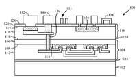
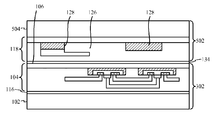
도 1은 실시예에 따른 칩셋(100)을 예시한다. 칩셋(100)은 제 1 SOI(silicon-on-insulator) 웨이퍼(104)가 결합된 유리, 석영 또는 사파이어와 같은 절연체로 형성된 시트(102)를 포함한다. 제 1 SOI 웨이퍼(104)는 시트(102)를 향하는 제 1 측면(108) 및 제 2 측면(110)을 갖는 제 1 기판층 또는 제 1 절연층(106)을 포함하고, 제 1 SOI 웨이퍼(104)는 또한 제 1 회로층(112)을 포함하고, 제 1 회로층(112)은 제 1 절연층(106)의 제 1 측면(108) 상의 복수의 CMOS 트랜지스터들(114) 및 연관된 와이어링을 포함한다. 이러한 CMOS 트랜지스터들(114) 및 다른 회로 엘리먼트들(예시되지 않음)은 디지털 신호 프로세싱을 위한 회로, 애플리케이션 또는 그래픽 프로세서들, 및/또는 기저대역 신호들을 처리하기 위한 회로를 포함할 수 있다. 제 1 SOI 웨이퍼(104)는, 제 1 회로층(112)이 제 1 SOI 웨이퍼(104)의 제 1 절연층(106)의 제 1 측면(108)과 시트(102) 사이에 위치되도록 제 1 접착층(116) 또는 다른 종래의 웨이퍼 결합 기술들을 사용하여 시트(102)에 결합된다. 1 illustrates a
제 2 SOI 웨이퍼(118)는 제 1 SOI 웨이퍼(104)에 접속된다. 제 2 SOI 웨이퍼(118)는 제 1 절연층(106)의 제 2 측면(110)을 향하는 제 1 측면(122) 및 제 2 측면(124)을 갖는 제 2 기판층 또는 제 2 절연층(120)을 포함한다. 제 2 SOI 웨이퍼(118)는 또한 제 2 회로층(126)을 포함하고, 제 2 회로층(126)은 제 2 회로층(126) 내에 부분적으로 또는 전체적으로 위치된 저항기(128) 및 커패시터(132) 및 인덕터(133)와 같은 패시브 엘리먼트들 또는 "패시브들" 및 제 2 절연층(120)의 제 2 측면(124) 상에 위치된 MEMS 디바이스 또는 센서(138)를 포함한다. 단일 저항기(128), 커패시터(132), 인덕터(133) 및 MEMS 디바이스(138)가 도 1에 예시되지만, 제 2 SOI 웨이퍼(118)는, 일부 경우들에서, 이러한 컴포넌트 형태들 중 하나 또는 둘만을 포함하거나 및/또는 이러한 별개의 컴포넌트들(CMOS 트랜지스터들과 같은 능동 회로를 포함함) 중 다수의 컴포넌트들을 포함할 수 있다. 제 2 SOI 웨이퍼(118)는, 제 2 회로층(126)이 제 2 절연층(120)의 제 1 측면(122)과 제 1 절연층(106)의 제 2 측면(110) 사이에 위치되도록 제 2 접착층(134)을 사용하여 제 1 절연층(106)의 제 2 측면(110)에 결합된다. 비아들(136)은 제 2 회로층(126)의 엘리먼트들을 제 1 회로층(112)의 엘리먼트들에 전기적으로 접속하고, 적절한 금속 접촉들(140)은 제 2 회로층(126) 및/또는 제 1 회로층(112) 내의 또는 상의 엘리먼트들을 칩셋(100) 외부의 디바이스들에 전기적으로 접속하기 위해 제 2 절연층(120)의 제 2 측면(124)에서 접속될 수 있다. The
유사한 칩셋이 사파이어, 석영 또는 유리와 같은 순수 절연체로 형성된 시트(102) 대신에 매립 산화물(SOI CMOS 기술에서의 경우와 같이)을 갖는 고저항 실리콘(Si) 기판 상에 구성되었지만, 비선형 기생 커패시턴스들이 RF 주파수들에서 SOI 기판 내의 고저항 Si와 매립 SiO2 사이의 계면에서 생성될 것이다. 이러한 기생 커패시턴스들은 RF 스위치들 및 전력 증폭기들에 대한 비선형성들 및 전력 처리 이슈들을 발생시킨다. 본원에 설명된 바와 같은 시트(102)의 사용은 실질적으로 비선형-기생-커패시턴스 문제를 제거하고, 하이-Q 패시브들을 포함할 수 있는 패시브들 및 CMOS 트랜지스터들(114)과 같은 CMOS 엘리먼트들이 SOI 웨이퍼들 상에서보다 훨씬 더 양호한 성능으로 동일한 칩셋(100)에서 함께 사용되도록 허용한다. Although a similar chipset is constructed on a high resistance silicon (Si) substrate with buried oxide (as in SOI CMOS technology) instead of
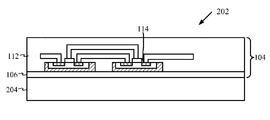
칩셋(100)의 다양한 제조 스테이지들이 도 2 내지 도 7에 예시되고, 칩셋(100)에 존재하고 도 1에서 논의된 엘리먼트들은 도 2 내지 도 7에서 동일한 참조 번호들에 의해 식별된다. 도 2는, 제 1 절연층(106) 및 제 1 회로층(112)이 형성된 제 1 실리콘 기판 또는 처리층(204)을 포함하는 제 1 스톡(stock) SOI 웨이퍼(202)를 예시한다. 제 1 스톡 SOI 웨이퍼(202)는 비용들을 감소시키는 것을 돕기 위해 종래의 벌크 실리콘 CMOS 웨이퍼를 포함할 수 있고, 이러한 경우에, 제 1 기판층(106)은 절연체를 포함하지 않을 것이지만, 대신에 제 1 회로층(112)의 엘리먼트들 바로 아래에 위치된 벌크 실리콘의 부분일 것이다. Various manufacturing stages of the
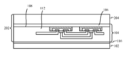
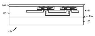
도 3은 반전되어 제 1 접착층(116)에 의해 시트(102)에 결합된 제 1 스톡 SOI 웨이퍼(202)를 도시하고, 제 1 절연층(106)의 제 1 측면(108)이 시트(102)를 향하고, 도 4는, 예를 들면, 원하는 양의 제 1 실리콘 처리층(204)을 선택적으로 제거하기 위한 CMP(chemical mechanical polishing) 또는 다른 적절한 프로세스에 의한 제 1 실리콘 처리층(204)의 제거에 의해 형성된 제 1 컴포넌트(302)를 도시한다. 도 5는, 제 2 절연층(120) 및 제 2 회로층(126)이 형성된 제 2 실리콘 기판 또는 처리층(504)을 포함하는 제 2 스톡 SOI 웨이퍼(502)를 예시한다. 도 6은 반전되어 제 1 컴포넌트(302)에 부착된 제 2 스톡 SOI 웨이퍼(502)를 도시하고, 제 2 스톡 SOI 웨이퍼(502)의 제 2 회로층(126)이 제 2 접착층(134)에 의해 제 1 절연층(106)에 결합된다. 도 7은, 제 2 스톡 SOI 웨이퍼(502) 및 제 1 컴포넌트(302)의 결합을 포함하는 제 2 컴포넌트(702)를 도시하고, 제 2 스톡 SOI 웨이퍼(502)의 제 2 실리콘 처리층(504)이 CMP 또는 다른 적절한 프로세스에 의해 제거된다. 비아들(136)은 또한 제 2 컴포넌트(702)에 형성되고, 금속 접촉들(140) 및 다른 BEOL(Back-End-of-the-Line) 컴포넌트들(패시브들, MEMS, 센서들 등을 포함함)의 부가는 도 1의 칩셋(100)을 발생시킨다. 3 illustrates a first
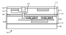
도 8은 제 1 실시예와 공통인 엘리먼트들이 동일한 참조 번호들로 식별되는 또 다른 실시예를 예시한다. 도 8은 시트(102), 제 1 SOI 웨이퍼(104) 및 제 2 SOI 웨이퍼(118)를 포함하는 제 2 칩셋(800)을 예시하고, 제 1 SOI 웨이퍼(104) 및 제 2 SOI 웨이퍼(118)는 제 3 SOI 웨이퍼(802)에 의해 이격된다. 제 3 SOI 웨이퍼(802)는 제 1 측면(806) 및 제 2 측면(808)을 갖는 제 3 기판층 또는 절연층(804), 및 제 3 절연층(804)의 제 1 측면(806) 상에 복수의 회로 엘리먼트를 포함하는 제 3 층(810)을 포함하고, 회로 엘리먼트들은 아날로그 회로(814) 및/또는 RF 컴포넌트들(816)을 포함할 수 있다. 제 3 SOI 웨이퍼(802)는, 제 3 SOI 웨이퍼(802)의 제 1 측면(806)이 제 1 SOI 웨이퍼(104)의 제 2 측면(110)을 향하도록 제 2 접착층(818)을 사용하여 제 1 SOI 웨이퍼(104)의 제 2 측면(110)에 부착된다. 제 2 SOI 웨이퍼(118)는, 제 2 SOI 웨이퍼(118)의 제 1 측면이 제 3 SOI 웨이퍼(802)의 제 2 측면(808)을 향하도록 제 3 접착층(820)에 의해 제 3 SOI 웨이퍼(802)의 제 2 측면(808)에 부착된다. 제 1 SOI 웨이퍼(104), 제 2 SOI 웨이퍼(118) 및 제 3 SOI 웨이퍼(802) 3 개 모두는 실질적으로 동일한 표면 영역들을 갖는다. 비아들(822)은 제 1 회로층(112), 제 2 회로층(126) 및 제 3 회로층(810)의 회로 컴포넌트들을 접속하고, 금속 접촉들(140)은 제 2 칩셋(800) 외부의 엘리먼트들에 접속들을 제공한다. 이러한 배열은 아날로그 회로(814) 및/또는 RF 컴포넌트들(816)이 커패시터(132)와 같은 패시브들 및 디지털 회로 엘리먼트들(114)과 동일한 칩셋에 포함되도록 허용하고, 콤팩트 패키지에서 많은 종래의 기능들을 수행하는 수직적으로 통합된 칩셋을 제공한다. Figure 8 illustrates another embodiment in which elements common to the first embodiment are identified by the same reference numerals. 8 illustrates a
시트(102)가 유리, 사파이어 또는 석영을 포함하는 것으로 설명되었지만, 시트(102)에 대한 유리의 사용이 일부 상황들에서 특히 유리할 수 있다. 첫째, 유리는 일반적으로 사파이어 또는 석영보다 더 낮은 비용을 갖는다. 다음에, 유리는 또한 사파이어보다 훨씬 더 낮은 유전 상수를 갖고, 이것은 기판으로부터 기생 커패시턴스를 상당히 감소시킨다. 마지막으로, 유리의 웨이퍼/패널 크기는 사파이어 및 석영보다 훨씬 더 클 수 있고, 이것은 더 큰 규모의 대량 생산 및 더 낮은 단위 원가를 허용할 수 있다. While the
개시된 실시예들의 칩셋들은 하나 이상의 반도체 다이들에 통합되거나, 셋 톱 박스, 음악 플레이어, 비디오 플레이어, 엔터테인먼트 유닛, 내비게이션 디바이스, 통신 디바이스들, PDA(personal digital assistant), 고정 위치 데이터 유닛, 및 컴퓨터와 같은 디바이스에 통합될 수 있다. The chipsets of the disclosed embodiments may be integrated into one or more semiconductor dies or may be integrated into a set top box, a music player, a video player, an entertainment unit, a navigation device, communication devices, a personal digital assistant (PDA) Can be integrated into the same device.
본원에 개시된 실시예들에 관련하여 설명된 방법들, 시퀀스들 및/또는 알고리즘들은 직접적으로 하드웨어로, 프로세서에 의해 실행되는 소프트웨어 모듈로, 또는 이 둘의 조합으로 구현될 수 있다. 소프트웨어 모듈은 RAM 메모리, 플래시 메모리, ROM 메모리, EPROM 메모리, EEPROM 메모리, 레지스터들, 하드 디스크, 제거 가능한 디스크, CD-ROM, 또는 당분야에 알려진 임의의 다른 형태의 저장 매체에 상주할 수 있다. 예시적인 저장 매체는, 프로세서가 저장 매체로부터 정보를 판독하고 정보를 저장 매체에 기록할 수 있도록 프로세서에 연결된다. 대안으로, 저장 매체는 프로세서에 통합될 수 있다. The methods, sequences, and / or algorithms described in connection with the embodiments disclosed herein may be embodied directly in hardware, in a software module executed by a processor, or in a combination of the two. The software module may reside in RAM memory, flash memory, ROM memory, EPROM memory, EEPROM memory, registers, a hard disk, a removable disk, a CD-ROM, or any other form of storage medium known in the art. An exemplary storage medium is coupled to the processor such that the processor can read information from, and write information to, the storage medium. Alternatively, the storage medium may be integrated into the processor.
앞서 말한 개시내용이 본 발명의 예시적인 실시예들을 보여주지만, 첨부된 청구항들에 의해 정의된 바와 같은 본 발명의 범위에서 벗어나지 않고, 다양한 변화들 및 수정들이 본원에서 이루어질 수 있다는 것이 유의되어야 한다. 본원에 설명된 본 발명의 실시예들에 따른 방법 청구항들의 기능들, 단계들 및/또는 동작들은 임의의 특정 순서로 수행될 필요는 없다. 또한, 본 발명의 엘리먼트들이 단수형으로 기술 또는 청구될 수 있지만, 단수형으로의 제한이 명시적으로 언급되지 않는다면, 복수형이 고려된다. It should be noted that while the foregoing disclosure shows illustrative embodiments of the invention, various changes and modifications can be made herein without departing from the scope of the invention as defined by the appended claims. The functions, steps and / or operations of the method claims according to embodiments of the invention described herein need not be performed in any particular order. Furthermore, elements of the invention may be described or claimed in a singular, but plural form is contemplated unless limitation to the singular is explicitly stated.
Claims (54)
유리, 석영 또는 사파이어의 시트,
제 1 기판층의 제 1 측면 상의 적어도 하나의 제 1 회로층을 포함하는 제 1 웨이퍼 ― 상기 제 1 웨이퍼는 상기 적어도 하나의 제 1 회로층이 상기 제 1 기판층과 상기 시트 사이에 위치되도록 상기 시트에 접속됨 ―, 및
제 2 기판층의 제 1 측면 상의 적어도 하나의 제 2 회로층을 포함하는 제 2 웨이퍼 ― 상기 제 2 웨이퍼는 상기 적어도 하나의 제 2 회로층이 상기 제 2 기판층과 상기 제 1 기판층 사이에 위치되도록 상기 제 1 기판층에 접속됨 ― 를 포함하는,
칩셋.As a chipset,
Sheets of glass, quartz or sapphire,
A first wafer comprising at least one first circuit layer on a first side of a first substrate layer, the first wafer having a first side and a second side, wherein the at least one first circuit layer is positioned between the first substrate layer and the sheet, Connected to the sheet -, and
A second wafer comprising at least one second circuit layer on a first side of a second substrate layer, the second wafer having a second circuit layer disposed between the second substrate layer and the first substrate layer Said first substrate layer being positioned on said first substrate layer,
Chipset.
상기 제 1 기판층은 제 1 절연층을 포함하고,
상기 제 2 기판층은 제 2 절연층을 포함하는,
칩셋.The method according to claim 1,
Wherein the first substrate layer comprises a first insulating layer,
Wherein the second substrate layer comprises a second insulating layer.
Chipset.
상기 제 1 웨이퍼 및 상기 제 2 웨이퍼 각각은 SOI(silicon-on-insulator) 웨이퍼를 포함하는,
칩셋.3. The method of claim 2,
Wherein each of the first wafer and the second wafer includes a silicon-on-insulator (SOI) wafer,
Chipset.
상기 적어도 하나의 제 1 회로층은 복수의 CMOS 트랜지스터들을 포함하는,
칩셋.The method of claim 3,
Wherein the at least one first circuit layer comprises a plurality of CMOS transistors,
Chipset.
상기 적어도 하나의 제 2 회로층은 적어도 하나의 패시브 회로 엘리먼트를 포함하거나 지지하는,
칩셋.The method of claim 3,
Said at least one second circuit layer comprising or supporting at least one passive circuit element,
Chipset.
상기 적어도 하나의 제 2 회로층은 적어도 하나의 MEMS(microelectromechanical) 엘리먼트를 포함하거나 지지하는,
칩셋.The method of claim 3,
Wherein the at least one second circuit layer comprises at least one microelectromechanical (MEMS) element,
Chipset.
상기 적어도 하나의 제 2 회로층은 적어도 하나의 센서를 포함하거나 지지하는,
칩셋.The method of claim 3,
Said at least one second circuit layer comprising or supporting at least one sensor,
Chipset.
상기 제 1 SOI 웨이퍼는 상기 시트에 직접적으로 결합되는,
칩셋.The method of claim 3,
Wherein the first SOI wafer is directly bonded to the sheet,
Chipset.
상기 제 2 SOI 웨이퍼는 상기 제 1 SOI 웨이퍼에 직접적으로 결합되는,
칩셋.The method of claim 3,
Wherein the second SOI wafer is directly coupled to the first SOI wafer,
Chipset.
상기 칩셋은 적어도 하나의 반도체 다이에 통합되는,
칩셋.The method of claim 3,
Wherein the chipset is integrated into at least one semiconductor die,
Chipset.
상기 칩셋은 셋 톱 박스, 음악 플레이어, 비디오 플레이어, 엔터테인먼트 유닛, 내비게이션 디바이스, 통신 디바이스, PDA(personal digital assistant), 고정 위치 데이터 유닛, 및 컴퓨터로 구성된 그룹으로부터 선택된 디바이스에 통합되는,
칩셋.The method of claim 3,
Wherein the chipset is integrated into a device selected from the group consisting of a set top box, a music player, a video player, an entertainment unit, a navigation device, a communication device, a personal digital assistant (PDA), a fixed location data unit,
Chipset.
상기 적어도 하나의 제 1 회로층은 복수의 CMOS 트랜지스터들을 포함하고,
상기 적어도 하나의 제 2 회로층은 적어도 하나의 패시브 컴포넌트 또는 적어도 하나의 MEMS 엘리먼트를 포함하거나 지지하고,
상기 제 1 SOI 웨이퍼는 상기 시트에 직접적으로 결합되고, 그리고
상기 제 2 SOI 웨이퍼는 상기 제 1 절연층에 직접적으로 결합되는,
칩셋.The method of claim 3,
Wherein the at least one first circuit layer comprises a plurality of CMOS transistors,
Wherein the at least one second circuit layer comprises or supports at least one passive component or at least one MEMS element,
The first SOI wafer is directly bonded to the sheet, and
Wherein the second SOI wafer is directly coupled to the first insulating layer,
Chipset.
상기 칩셋은, SOI를 포함하고 제 3 절연층의 제 1 측면 상의 적어도 하나의 제 3 회로층을 갖는 제 3 웨이퍼를 포함하고,
상기 제 3 웨이퍼는 상기 적어도 하나의 제 3 회로층이 상기 제 1 절연층과 상기 제 2 절연층 사이에 위치되도록 상기 제 1 웨이퍼에 접속되는,
칩셋.The method of claim 3,
The chipset comprising a third wafer comprising SOI and having at least one third circuit layer on a first side of a third insulating layer,
Wherein the third wafer is connected to the first wafer such that the at least one third circuit layer is positioned between the first insulating layer and the second insulating layer.
Chipset.
상기 적어도 하나의 제 3 회로층은 CMOS 트랜지스터들을 포함하는,
칩셋.14. The method of claim 13,
Said at least one third circuit layer comprising CMOS transistors,
Chipset.
상기 제 2 웨이퍼는 상기 적어도 하나의 제 2 회로층이 상기 제 2 절연층과 상기 제 3 절연층 사이에 위치되도록 상기 제 3 웨이퍼에 직접적으로 결합되는,
칩셋.14. The method of claim 13,
The second wafer being directly coupled to the third wafer such that the at least one second circuit layer is positioned between the second insulating layer and the third insulating layer,
Chipset.
상기 적어도 하나의 제 1 회로층은 디지털 회로를 포함하고,
상기 적어도 하나의 제 3 회로층은 아날로그 회로를 포함하는,
칩셋.14. The method of claim 13,
Wherein the at least one first circuit layer comprises a digital circuit,
Said at least one third circuit layer comprising analog circuitry,
Chipset.
상기 적어도 하나의 제 1 회로층은 디지털 회로를 포함하고,
상기 적어도 하나의 제 2 회로층은 패시브 디바이스 또는 MEMS 엘리먼트를 포함하거나 지지하고,
상기 적어도 하나의 제 3 회로층은 아날로그 또는 RF 회로를 포함하는,
칩셋.14. The method of claim 13,
Wherein the at least one first circuit layer comprises a digital circuit,
The at least one second circuit layer comprising or supporting a passive device or MEMS element,
Said at least one third circuit layer comprising an analog or RF circuit,
Chipset.
상기 제 1 기판층의 표면 영역은 상기 제 2 기판층의 표면 영역과 실질적으로 동일하고,
상기 제 2 기판층의 표면 영역은 상기 제 3 기판층의 표면 영역과 실질적으로 동일한,
칩셋.14. The method of claim 13,
Wherein the surface area of the first substrate layer is substantially the same as the surface area of the second substrate layer,
Wherein the surface area of the second substrate layer is substantially the same as the surface area of the third substrate layer,
Chipset.
제 1 실리콘 기판 및 상기 제 1 실리콘 기판 상의 적어도 하나의 제 1 회로층을 포함하는 제 1 웨이퍼를 제공하는 단계,
상기 적어도 하나의 제 1 회로층을 유리, 석영 또는 사파이어의 시트에 접속하고, 이어서 상기 제 1 실리콘 기판의 부분을 제거하는 단계,
제 2 실리콘 기판 및 상기 제 2 실리콘 기판 상의 적어도 하나의 제 2 회로층을 포함하는 제 2 웨이퍼를 제공하는 단계, 및
상기 적어도 하나의 제 2 회로층을 상기 제 1 실리콘 기판에 접속하고, 이어서 상기 제 2 실리콘 기판의 부분을 제거하는 단계를 포함하는,
칩셋을 형성하는 방법.CLAIMS 1. A method of forming a chipset,
Providing a first wafer comprising a first silicon substrate and at least one first circuit layer on the first silicon substrate,
Connecting said at least one first circuit layer to a sheet of glass, quartz or sapphire, and then removing portions of said first silicon substrate;
Providing a second wafer comprising a second silicon substrate and at least one second circuit layer on the second silicon substrate, and
Connecting said at least one second circuit layer to said first silicon substrate, and subsequently removing a portion of said second silicon substrate.
A method for forming a chipset.
상기 제 1 실리콘 기판과 상기 제 2 실리콘 기판 사이에 절연층을 제공하는 단계를 포함하는,
칩셋을 형성하는 방법.20. The method of claim 19,
And providing an insulating layer between the first silicon substrate and the second silicon substrate.
A method for forming a chipset.
상기 적어도 하나의 제 2 회로층을 상기 제 1 실리콘 기판에 접속하는 단계는, 상기 적어도 하나의 제 2 회로층을 상기 절연층에 직접적으로 결합하는 단계를 포함하는,
칩셋을 형성하는 방법.21. The method of claim 20,
Wherein coupling the at least one second circuit layer to the first silicon substrate comprises coupling the at least one second circuit layer directly to the insulation layer.
A method for forming a chipset.
상기 제 1 실리콘 기판은 제 1 절연층을 포함하고, 실리콘의 제 1 본체는 상기 제 1 절연층의 제 1 측면 상에 위치되고, 상기 적어도 하나의 제 1 회로층은 상기 제 1 절연층의 제 2 측면 상에 위치되고, 상기 제 1 실리콘 기판의 부분을 제거하는 단계는 상기 실리콘의 제 1 본체를 제거하는 단계를 포함하고, 그리고
상기 제 2 실리콘 기판은 제 2 절연층을 포함하고, 실리콘의 제 2 본체는 상기 제 2 절연층의 제 1 측면 상에 위치되고, 상기 적어도 하나의 제 2 회로층은 상기 제 2 절연층의 제 2 측면 상에 위치되고, 상기 제 2 실리콘 기판의 부분을 제거하는 단계는 상기 실리콘의 제 2 본체를 제거하는 단계를 포함하는,
칩셋을 형성하는 방법.20. The method of claim 19,
Wherein the first silicon substrate comprises a first insulating layer, a first body of silicon is located on a first side of the first insulating layer, and the at least one first circuit layer comprises a first insulating layer Wherein removing the portion of the first silicon substrate comprises removing the first body of silicon; and
Wherein the second silicon substrate comprises a second insulating layer, a second body of silicon is located on a first side of the second insulating layer, and the at least one second circuit layer comprises a second insulating layer Wherein removing the portion of the second silicon substrate comprises removing the second body of silicon.
A method for forming a chipset.
상기 방법은 상기 제 1 실리콘 기판과 상기 제 2 실리콘 기판 사이에 제 1 절연층을 제공하는 단계를 포함하고,
상기 제 2 실리콘 기판은 제 2 절연층을 포함하고, 실리콘의 본체는 상기 제 2 절연층의 제 1 측면 상에 위치되고, 상기 적어도 하나의 제 2 회로층은 상기 제 2 절연층의 제 2 측면 상에 위치되고, 상기 제 2 실리콘 기판의 부분을 제거하는 단계는 상기 실리콘의 본체를 제거하는 단계를 포함하는,
칩셋을 형성하는 방법.20. The method of claim 19,
The method includes providing a first insulating layer between the first silicon substrate and the second silicon substrate,
Wherein the second silicon substrate comprises a second insulating layer, the body of silicon is located on a first side of the second insulating layer, and the at least one second circuit layer is located on a second side of the second insulating layer Wherein removing the portion of the second silicon substrate comprises removing the body of silicon.
A method for forming a chipset.
상기 제 1 절연층을 통해 연장되는 비아(via)를 형성하고, 상기 적어도 하나의 제 1 회로층의 부분을 상기 적어도 하나의 제 2 회로층의 부분에 전기적으로 접속하는 단계를 포함하는,
칩셋을 형성하는 방법.24. The method of claim 23,
Forming a via extending through the first insulating layer and electrically connecting a portion of the at least one first circuit layer to a portion of the at least one second circuit layer.
A method for forming a chipset.
상기 적어도 하나의 제 1 회로층은 복수의 CMOS 트랜지스터들을 포함하는,
칩셋을 형성하는 방법.24. The method of claim 23,
Wherein the at least one first circuit layer comprises a plurality of CMOS transistors,
A method for forming a chipset.
상기 적어도 하나의 제 2 회로층은 적어도 하나의 패시브(passive) 컴포넌트를 포함하는,
칩셋을 형성하는 방법.24. The method of claim 23,
Wherein the at least one second circuit layer comprises at least one passive component,
A method for forming a chipset.
상기 적어도 하나의 제 2 회로층은 적어도 하나의 아날로그/RF 컴포넌트를 포함하는,
칩셋을 형성하는 방법.24. The method of claim 23,
Wherein the at least one second circuit layer comprises at least one analog / RF component.
A method for forming a chipset.
상기 적어도 하나의 제 2 회로는 적어도 하나의 MEMS(microelectromechanical) 또는 센서 컴포넌트를 포함하는,
칩셋을 형성하는 방법.24. The method of claim 23,
Wherein the at least one second circuit comprises at least one microelectromechanical (MEMS) or sensor component,
A method for forming a chipset.
상기 적어도 하나의 제 1 회로층을 유리, 석영 또는 사파이어의 시트에 접속하는 단계는 상기 적어도 하나의 제 1 회로층을 상기 유리, 석영 또는 사파이어의 시트에 직접적으로 결합하는 단계를 포함하는,
칩셋을 형성하는 방법.24. The method of claim 23,
Wherein connecting the at least one first circuit layer to a sheet of glass, quartz or sapphire comprises directly bonding the at least one first circuit layer to the sheet of glass, quartz or sapphire.
A method for forming a chipset.
제 3 실리콘 기판 및 상기 제 3 실리콘 기판 상의 적어도 하나의 제 3 회로층을 포함하는 제 3 웨이퍼를 제공하고, 상기 적어도 하나의 제 3 회로층을 상기 제 2 실리콘 기판에 접속하고, 이어서 상기 제 3 실리콘 기판의 부분을 제거하는 단계를 포함하는,
칩셋을 형성하는 방법.20. The method of claim 19,
Providing a third wafer comprising a third silicon substrate and at least one third circuit layer on the third silicon substrate, connecting the at least one third circuit layer to the second silicon substrate, Removing the portion of the silicon substrate;
A method for forming a chipset.
상기 제 1 실리콘 기판은 제 1 절연층을 포함하고, 실리콘의 제 1 본체는 상기 제 1 절연층의 제 1 측면 상에 위치되고, 상기 적어도 하나의 제 1 회로층은 상기 제 1 절연층의 제 2 측면 상에 위치되고, 상기 제 1 실리콘 기판의 부분을 제거하는 단계는 상기 실리콘의 제 1 본체를 제거하는 단계를 포함하고,
상기 제 2 실리콘 기판은 제 2 절연층을 포함하고, 실리콘의 제 2 본체는 상기 제 2 절연층의 제 1 측면 상에 위치되고, 상기 적어도 하나의 제 2 회로층은 상기 제 2 절연층의 제 2 측면 상에 위치되고, 상기 제 2 실리콘 기판의 부분을 제거하는 단계는 상기 실리콘의 제 2 본체를 제거하는 단계를 포함하고, 그리고
상기 제 3 실리콘 기판은 제 3 절연층을 포함하고, 실리콘의 제 3 본체는 상기 제 3 절연층의 제 1 측면 상에 위치되고, 상기 적어도 하나의 제 3 회로층은 상기 제 3 절연층의 제 2 측면 상에 위치되고, 상기 제 3 실리콘 기판의 부분을 제거하는 단계는 상기 실리콘의 제 3 본체를 제거하는 단계를 포함하는,
칩셋을 형성하는 방법.31. The method of claim 30,
Wherein the first silicon substrate comprises a first insulating layer, a first body of silicon is located on a first side of the first insulating layer, and the at least one first circuit layer comprises a first insulating layer Wherein removing the portion of the first silicon substrate comprises removing the first body of silicon,
Wherein the second silicon substrate comprises a second insulating layer, a second body of silicon is located on a first side of the second insulating layer, and the at least one second circuit layer comprises a second insulating layer Wherein removing the portion of the second silicon substrate comprises removing the second body of silicon; and
Wherein the third silicon substrate comprises a third insulating layer, a third body of silicon is located on a first side of the third insulating layer, and the at least one third circuit layer comprises a third insulating layer Wherein removing the third portion of the third silicon substrate comprises removing the third body of silicon.
A method for forming a chipset.
상기 적어도 제 3 회로층을 상기 제 2 절연층에 접속하는 단계는 상기 적어도 하나의 제 3 회로층을 상기 제 2 절연층에 직접적으로 결합하는 단계를 포함하는,
칩셋을 형성하는 방법.32. The method of claim 31,
Wherein connecting at least the third circuit layer to the second insulating layer comprises coupling the at least one third circuit layer directly to the second insulating layer.
A method for forming a chipset.
상기 적어도 하나의 제 1 회로층은 디지털 회로에 대한 복수의 CMOS 트랜지스터들을 포함하고,
상기 적어도 하나의 제 2 회로층은 아날로그 또는 RF 회로에 대한 복수의 CMOS 트랜지스터들을 포함하고, 그리고
상기 적어도 하나의 제 3 회로층은 적어도 하나의 패시브 컴포넌트 또는 적어도 하나의 MEMS 또는 센서 엘리먼트를 포함하거나 지지하는,
칩셋을 형성하는 방법.32. The method of claim 31,
Wherein the at least one first circuit layer comprises a plurality of CMOS transistors for a digital circuit,
Wherein the at least one second circuit layer comprises a plurality of CMOS transistors for an analog or RF circuit, and
The at least one third circuit layer comprising or supporting at least one passive component or at least one MEMS or sensor element,
A method for forming a chipset.
상기 제 1 절연층의 표면 영역은 상기 제 2 절연층의 표면 영역과 실질적으로 동일하고,
상기 제 2 절연층의 표면 영역은 상기 제 3 절연층의 표면 영역과 실질적으로 동일한,
칩셋을 형성하는 방법.32. The method of claim 31,
The surface region of the first insulating layer is substantially the same as the surface region of the second insulating layer,
Wherein the surface region of the second insulating layer is substantially the same as the surface region of the third insulating layer,
A method for forming a chipset.
상기 제 1 웨이퍼 및 상기 제 2 웨이퍼를 적어도 하나의 반도체 다이에 통합하는 단계를 포함하는,
칩셋을 형성하는 방법.20. The method of claim 19,
And integrating the first wafer and the second wafer into at least one semiconductor die.
A method for forming a chipset.
셋 톱 박스, 음악 플레이어, 비디오 플레이어, 엔터테인먼트 유닛, 내비게이션 디바이스, 통신 디바이스, PDA(personal digital assistant), 고정 위치 데이터 유닛, 및 컴퓨터로 구성된 그룹으로부터 선택된 디바이스에 상기 제 1 웨이퍼 및 상기 제 2 웨이퍼를 통합하는 단계를 포함하는,
칩셋을 형성하는 방법.20. The method of claim 19,
The first wafer and the second wafer are transferred to a device selected from the group consisting of a set top box, a music player, a video player, an entertainment unit, a navigation device, a communication device, a personal digital assistant (PDA) ≪ / RTI >
A method for forming a chipset.
웨이퍼를 지지하기 위한 절연체 시트 수단,
제 1 기판층의 제 1 측면 상의 신호들을 프로세싱하기 위한 적어도 하나의 제 1 회로 수단을 포함하는 제 1 웨이퍼 ― 상기 제 1 웨이퍼는 상기 적어도 하나의 제 1 회로 수단이 상기 제 1 기판층과 상기 절연체 시트 수단 사이에 위치되도록 상기 절연체 시트 수단에 접속됨 ― , 및
제 2 기판층의 제 1 측면 상의 신호들을 프로세싱하기 위한 적어도 하나의 제 2 회로 수단을 포함하는 제 2 웨이퍼 ― 상기 제 2 웨이퍼는 상기 적어도 하나의 제 2 회로 수단이 상기 제 2 기판층과 상기 제 1 기판층 사이에 위치되도록 상기 제 1 기판층에 접속됨 ― 를 포함하는,
칩셋.As a chipset,
Insulator sheet means for supporting the wafer,
A first wafer comprising at least one first circuit means for processing signals on a first side of a first substrate layer, the first wafer being characterized in that the at least one first circuit means comprises a first substrate layer, Connected to the insulator sheet means to be positioned between the sheet means, and
A second wafer comprising at least one second circuit means for processing signals on a first side of a second substrate layer, the second wafer being configured such that the at least one second circuit means comprises a second substrate layer, And a second substrate layer disposed between the first substrate layer and the second substrate layer,
Chipset.
상기 제 1 기판층은 상기 제 2 웨이퍼로부터 상기 적어도 하나의 제 1 회로 수단을 절연하기 위한 제 1 절연층 수단을 포함하는,
칩셋.39. The method of claim 37,
Wherein the first substrate layer comprises a first insulating layer means for insulating the at least one first circuit means from the second wafer.
Chipset.
상기 제 1 웨이퍼 및 상기 제 2 웨이퍼 각각은 SOI(silicon-on-insulator) 웨이퍼를 포함하는,
칩셋.39. The method of claim 37,
Wherein each of the first wafer and the second wafer includes a silicon-on-insulator (SOI) wafer,
Chipset.
상기 적어도 하나의 제 1 회로 수단은 복수의 CMOS 트랜지스터들을 포함하는,
칩셋.39. The method of claim 37,
Wherein the at least one first circuit means comprises a plurality of CMOS transistors,
Chipset.
상기 적어도 하나의 제 2 회로 수단은 적어도 하나의 패시브 회로 엘리먼트를 포함하거나 지지하는,
칩셋.39. The method of claim 37,
Said at least one second circuit means comprising or supporting at least one passive circuit element,
Chipset.
상기 적어도 하나의 제 2 회로 수단은 적어도 하나의 MEMS(microelectromechanical) 엘리먼트 또는 적어도 하나의 센서를 포함하거나 지지하는,
칩셋.39. The method of claim 37,
Said at least one second circuit means comprising or supporting at least one MEMS (microelectromechanical) element or at least one sensor,
Chipset.
상기 칩셋은 적어도 하나의 반도체 다이에 통합되는,
칩셋.39. The method of claim 37,
Wherein the chipset is integrated into at least one semiconductor die,
Chipset.
상기 칩셋은 셋 톱 박스, 음악 플레이어, 비디오 플레이어, 엔터테인먼트 유닛, 내비게이션 디바이스, 통신 디바이스, PDA(personal digital assistant), 고정 위치 데이터 유닛, 및 컴퓨터로 구성된 그룹으로부터 선택된 디바이스에 통합되는,
칩셋.39. The method of claim 37,
Wherein the chipset is integrated into a device selected from the group consisting of a set top box, a music player, a video player, an entertainment unit, a navigation device, a communication device, a personal digital assistant (PDA), a fixed location data unit,
Chipset.
상기 적어도 하나의 제 1 회로 수단은 복수의 CMOS 트랜지스터들을 포함하고,
상기 적어도 하나의 제 2 회로 수단은 적어도 하나의 패시브 컴포넌트 또는 적어도 하나의 MEMS 엘리먼트를 포함하거나 지원하고,
상기 제 1 웨이퍼는 상기 절연체 시트 수단에 직접적으로 결합되고, 그리고
상기 제 2 웨이퍼는 상기 제 1 기판층에 직접적으로 결합되는,
칩셋.39. The method of claim 37,
Wherein the at least one first circuit means comprises a plurality of CMOS transistors,
Wherein the at least one second circuit means comprises or supports at least one passive component or at least one MEMS element,
The first wafer is directly coupled to the insulator sheet means, and
Wherein the second wafer is directly coupled to the first substrate layer,
Chipset.
상기 절연체 시트 수단은 유리의 시트 또는 석영의 시트 또는 사파이어의 시트를 포함하는,
칩셋.39. The method of claim 37,
Wherein the insulator sheet means comprises a sheet of glass or a sheet of quartz or a sheet of sapphire,
Chipset.
제 1 실리콘 기판 및 상기 제 1 실리콘 기판 상의 적어도 하나의 제 1 회로층을 포함하는 제 1 웨이퍼를 제공하기 위한 단계들,
상기 적어도 하나의 제 1 회로층을 유리, 석영 또는 사파이어의 시트에 접속하기 위한 단계들 및 이어서 상기 제 1 실리콘 기판의 부분을 제거하기 위한 단계들,
제 2 실리콘 기판 및 상기 제 2 실리콘 기판 상의 적어도 하나의 제 2 회로층을 포함하는 제 2 웨이퍼를 제공하기 위한 단계들, 및
상기 적어도 하나의 제 2 회로층을 상기 제 1 실리콘 기판에 접속하기 위한 단계들 및 이어서 상기 제 2 실리콘 기판의 부분을 제거하기 위한 단계들을 포함하는,
칩셋을 형성하는 방법.CLAIMS 1. A method of forming a chipset,
Providing a first wafer comprising a first silicon substrate and at least one first circuit layer on the first silicon substrate,
Steps for connecting said at least one first circuit layer to a sheet of glass, quartz or sapphire, and subsequently removing portions of said first silicon substrate,
Providing a second wafer comprising a second silicon substrate and at least one second circuit layer on the second silicon substrate; and
The method comprising: connecting the at least one second circuit layer to the first silicon substrate; and subsequently removing portions of the second silicon substrate.
A method for forming a chipset.
상기 제 1 실리콘 기판과 상기 제 2 실리콘 기판 사이에 절연층을 제공하기 위한 단계들을 포함하는,
칩셋을 형성하는 방법.49. The method of claim 47,
And providing an insulating layer between the first silicon substrate and the second silicon substrate.
A method for forming a chipset.
상기 제 1 실리콘 기판은 제 1 절연층을 포함하고, 실리콘의 제 1 본체는 상기 제 1 절연층의 제 1 측면 상에 위치되고, 상기 적어도 하나의 제 1 회로층은 상기 제 1 절연층의 제 2 측면 상에 위치되고, 상기 제 1 실리콘 기판의 부분을 제거하는 단계는 상기 실리콘의 제 1 본체를 제거하는 단계들을 포함하고, 그리고
상기 제 2 실리콘 기판은 제 2 절연층을 포함하고, 실리콘의 제 2 본체는 상기 제 2 절연층의 제 1 측면 상에 위치되고, 상기 적어도 하나의 제 2 회로층은 상기 제 2 절연층의 제 2 측면 상에 위치되고, 상기 제 2 실리콘 기판의 부분을 제거하는 단계는 상기 실리콘의 제 2 본체를 제거하는 단계들을 포함하는,
칩셋을 형성하는 방법.49. The method of claim 47,
Wherein the first silicon substrate comprises a first insulating layer, a first body of silicon is located on a first side of the first insulating layer, and the at least one first circuit layer comprises a first insulating layer Wherein removing the portion of the first silicon substrate comprises removing the first body of silicon; and
Wherein the second silicon substrate comprises a second insulating layer, a second body of silicon is located on a first side of the second insulating layer, and the at least one second circuit layer comprises a second insulating layer Wherein removing the portion of the second silicon substrate comprises removing the second body of silicon.
A method for forming a chipset.
상기 적어도 하나의 제 2 회로층은 적어도 하나의 패시브 컴포넌트를 포함하는,
칩셋을 형성하는 방법.49. The method of claim 47,
Wherein the at least one second circuit layer comprises at least one passive component,
A method for forming a chipset.
제 3 실리콘 기판 및 상기 제 3 실리콘 기판 상의 적어도 하나의 제 3 회로층을 포함하는 제 3 웨이퍼를 제공하기 위한 단계들, 상기 적어도 하나의 제 3 회로층을 상기 제 2 실리콘 기판에 접속하기 위한 단계들 및 이어서 상기 제 3 실리콘 기판의 부분을 제거하기 위한 단계들을 포함하는,
칩셋을 형성하는 방법.49. The method of claim 47,
Providing a third wafer comprising a third silicon substrate and at least one third circuit layer on the third silicon substrate; connecting the at least one third circuit layer to the second silicon substrate; And subsequently removing portions of the third silicon substrate.
A method for forming a chipset.
상기 제 1 실리콘 기판은 제 1 절연층을 포함하고, 실리콘의 제 1 본체는 상기 제 1 절연층의 제 1 측면 상에 위치되고, 상기 적어도 하나의 제 1 회로층은 상기 제 1 절연층의 제 2 측면 상에 위치되고, 상기 제 1 실리콘 기판의 부분을 제거하는 단계는 상기 실리콘의 제 1 본체를 제거하는 단계들을 포함하고,
상기 제 2 실리콘 기판은 제 2 절연층을 포함하고, 실리콘의 제 2 본체는 상기 제 2 절연층의 제 1 측면 상에 위치되고, 상기 적어도 하나의 제 2 회로층은 상기 제 2 절연층의 제 2 측면 상에 위치되고, 상기 제 2 실리콘 기판의 부분을 제거하는 단계는 상기 실리콘의 제 2 본체를 제거하는 단계들을 포함하고, 그리고
상기 제 3 실리콘 기판은 제 3 절연층을 포함하고, 실리콘의 제 3 본체는 상기 제 3 절연층의 제 1 측면 상에 위치되고, 상기 적어도 하나의 제 3 회로층은 상기 제 3 절연층의 제 2 측면 상에 위치되고, 상기 제 3 실리콘 기판의 부분을 제거하는 단계는 상기 실리콘의 제 3 본체를 제거하는 단계들을 포함하는,
칩셋을 형성하는 방법.49. The method of claim 47,
Wherein the first silicon substrate comprises a first insulating layer, a first body of silicon is located on a first side of the first insulating layer, and the at least one first circuit layer comprises a first insulating layer Wherein removing the portion of the first silicon substrate comprises removing the first body of silicon,
Wherein the second silicon substrate comprises a second insulating layer, a second body of silicon is located on a first side of the second insulating layer, and the at least one second circuit layer comprises a second insulating layer Wherein removing the portion of the second silicon substrate comprises removing the second body of silicon; and
Wherein the third silicon substrate comprises a third insulating layer, a third body of silicon is located on a first side of the third insulating layer, and the at least one third circuit layer comprises a third insulating layer Wherein removing the third portion of the third silicon substrate comprises removing the third body of silicon.
A method for forming a chipset.
상기 제 1 웨이퍼 및 상기 제 2 SOI 웨이퍼를 적어도 하나의 반도체 다이에 통합하기 위한 단계들을 포함하는,
칩셋을 형성하는 방법.49. The method of claim 47,
And integrating the first wafer and the second SOI wafer into at least one semiconductor die.
A method for forming a chipset.
셋 톱 박스, 음악 플레이어, 비디오 플레이어, 엔터테인먼트 유닛, 내비게이션 디바이스, 통신 디바이스, PDA(personal digital assistant), 고정 위치 데이터 유닛, 및 컴퓨터로 구성된 그룹으로부터 선택된 디바이스에 상기 제 1 웨이퍼 및 상기 제 2 SOI 웨이퍼를 통합하기 위한 단계들을 포함하는,
칩셋을 형성하는 방법.49. The method of claim 47,
To the device selected from the group consisting of a set top box, a music player, a video player, an entertainment unit, a navigation device, a communication device, a personal digital assistant (PDA), a fixed location data unit, And < RTI ID = 0.0 >
A method for forming a chipset.
Applications Claiming Priority (5)
| Application Number | Priority Date | Filing Date | Title |
|---|---|---|---|
| US201161560471P | 2011-11-16 | 2011-11-16 | |
| US61/560,471 | 2011-11-16 | ||
| US13/356,717 | 2012-01-24 | ||
| US13/356,717 US9496255B2 (en) | 2011-11-16 | 2012-01-24 | Stacked CMOS chipset having an insulating layer and a secondary layer and method of forming same |
| PCT/US2012/065644 WO2013075007A1 (en) | 2011-11-16 | 2012-11-16 | Stacked chipset having an insulating layer and a secondary layer and method of forming same |
Related Child Applications (1)
| Application Number | Title | Priority Date | Filing Date |
|---|---|---|---|
| KR1020167009373A Division KR101759689B1 (en) | 2011-11-16 | 2012-11-16 | Stacked chipset having an insulating layer and a secondary layer and method of forming same |
Publications (1)
| Publication Number | Publication Date |
|---|---|
| KR20140100526A true KR20140100526A (en) | 2014-08-14 |
Family
ID=48280458
Family Applications (2)
| Application Number | Title | Priority Date | Filing Date |
|---|---|---|---|
| KR1020167009373A KR101759689B1 (en) | 2011-11-16 | 2012-11-16 | Stacked chipset having an insulating layer and a secondary layer and method of forming same |
| KR1020147016198A KR20140100526A (en) | 2011-11-16 | 2012-11-16 | Stacked chipset having an insulating layer and a secondary layer and method of forming same |
Family Applications Before (1)
| Application Number | Title | Priority Date | Filing Date |
|---|---|---|---|
| KR1020167009373A KR101759689B1 (en) | 2011-11-16 | 2012-11-16 | Stacked chipset having an insulating layer and a secondary layer and method of forming same |
Country Status (7)
| Country | Link |
|---|---|
| US (1) | US9496255B2 (en) |
| EP (1) | EP2780942A1 (en) |
| JP (2) | JP5937225B2 (en) |
| KR (2) | KR101759689B1 (en) |
| CN (1) | CN104054175B (en) |
| IN (1) | IN2014MN01027A (en) |
| WO (1) | WO2013075007A1 (en) |
Families Citing this family (48)
| Publication number | Priority date | Publication date | Assignee | Title |
|---|---|---|---|---|
| CN104058363B (en) * | 2013-03-22 | 2016-01-20 | 上海丽恒光微电子科技有限公司 | Based on the display unit and forming method thereof of MEMS transmissive light valve |
| US9418985B2 (en) | 2013-07-16 | 2016-08-16 | Qualcomm Incorporated | Complete system-on-chip (SOC) using monolithic three dimensional (3D) integrated circuit (IC) (3DIC) technology |
| US9032353B2 (en) | 2013-10-10 | 2015-05-12 | Taiwan Semiconductor Manufacturing Co., Ltd. | Method and system for three-dimensional layout design of integrated circuit elements in stacked CMOS |
| US9257407B2 (en) * | 2013-10-28 | 2016-02-09 | Qualcomm Incorporated | Heterogeneous channel material integration into wafer |
| US9443758B2 (en) * | 2013-12-11 | 2016-09-13 | Taiwan Semiconductor Manufacturing Co., Ltd. | Connecting techniques for stacked CMOS devices |
| US10079170B2 (en) | 2014-01-23 | 2018-09-18 | Globalwafers Co., Ltd. | High resistivity SOI wafers and a method of manufacturing thereof |
| US9786613B2 (en) * | 2014-08-07 | 2017-10-10 | Qualcomm Incorporated | EMI shield for high frequency layer transferred devices |
| US20160043108A1 (en) * | 2014-08-07 | 2016-02-11 | Silanna Semiconductor U.S.A., Inc. | Semiconductor Structure with Multiple Active Layers in an SOI Wafer |
| US9899499B2 (en) | 2014-09-04 | 2018-02-20 | Sunedison Semiconductor Limited (Uen201334164H) | High resistivity silicon-on-insulator wafer manufacturing method for reducing substrate loss |
| US10224233B2 (en) | 2014-11-18 | 2019-03-05 | Globalwafers Co., Ltd. | High resistivity silicon-on-insulator substrate comprising a charge trapping layer formed by He-N2 co-implantation |
| JP6650463B2 (en) | 2014-11-18 | 2020-02-19 | グローバルウェーハズ カンパニー リミテッドGlobalWafers Co.,Ltd. | Method of manufacturing high resistivity semiconductor-on-insulator wafer with charge trapping layer |
| EP3573094B1 (en) | 2014-11-18 | 2023-01-04 | GlobalWafers Co., Ltd. | High resistivity semiconductor-on-insulator wafer and a method of manufacturing |
| WO2016081363A1 (en) * | 2014-11-18 | 2016-05-26 | Sunedison Semiconductor Limited | A system-on-chip on a semiconductor-on-insulator wafer and a method of manufacturing |
| EP4120320A1 (en) | 2015-03-03 | 2023-01-18 | GlobalWafers Co., Ltd. | Charge trapping polycrystalline silicon films on silicon substrates with controllable film stress |
| JP6637515B2 (en) | 2015-03-17 | 2020-01-29 | グローバルウェーハズ カンパニー リミテッドGlobalWafers Co.,Ltd. | Thermally stable charge trapping layer for use in the fabrication of semiconductor-on-insulator structures |
| US9881832B2 (en) | 2015-03-17 | 2018-01-30 | Sunedison Semiconductor Limited (Uen201334164H) | Handle substrate for use in manufacture of semiconductor-on-insulator structure and method of manufacturing thereof |
| US10304722B2 (en) | 2015-06-01 | 2019-05-28 | Globalwafers Co., Ltd. | Method of manufacturing semiconductor-on-insulator |
| US10332782B2 (en) | 2015-06-01 | 2019-06-25 | Globalwafers Co., Ltd. | Method of manufacturing silicon germanium-on-insulator |
| US20160379943A1 (en) * | 2015-06-25 | 2016-12-29 | Skyworks Solutions, Inc. | Method and apparatus for high performance passive-active circuit integration |
| US20170033135A1 (en) * | 2015-07-28 | 2017-02-02 | Skyworks Solutions, Inc. | Integrated passive device on soi substrate |
| US9768109B2 (en) * | 2015-09-22 | 2017-09-19 | Qualcomm Incorporated | Integrated circuits (ICS) on a glass substrate |
| JP6585978B2 (en) | 2015-09-24 | 2019-10-02 | ラピスセミコンダクタ株式会社 | Semiconductor device and manufacturing method of semiconductor device |
| CN108780776B (en) | 2015-11-20 | 2023-09-29 | 环球晶圆股份有限公司 | Manufacturing method for flattening semiconductor surface |
| US10256863B2 (en) * | 2016-01-11 | 2019-04-09 | Qualcomm Incorporated | Monolithic integration of antenna switch and diplexer |
| US9831115B2 (en) | 2016-02-19 | 2017-11-28 | Sunedison Semiconductor Limited (Uen201334164H) | Process flow for manufacturing semiconductor on insulator structures in parallel |
| WO2017142704A1 (en) | 2016-02-19 | 2017-08-24 | Sunedison Semiconductor Limited | High resistivity silicon-on-insulator substrate comprising a charge trapping layer formed on a substrate with a rough surface |
| US10622247B2 (en) | 2016-02-19 | 2020-04-14 | Globalwafers Co., Ltd. | Semiconductor on insulator structure comprising a buried high resistivity layer |
| US10573550B2 (en) | 2016-03-07 | 2020-02-25 | Globalwafers Co., Ltd. | Semiconductor on insulator structure comprising a plasma oxide layer and method of manufacture thereof |
| WO2017155804A1 (en) | 2016-03-07 | 2017-09-14 | Sunedison Semiconductor Limited | Method of manufacturing a semiconductor on insulator structure by a pressurized bond treatment |
| EP3427293B1 (en) | 2016-03-07 | 2021-05-05 | Globalwafers Co., Ltd. | Semiconductor on insulator structure comprising a low temperature flowable oxide layer and method of manufacture thereof |
| US11114332B2 (en) | 2016-03-07 | 2021-09-07 | Globalwafers Co., Ltd. | Semiconductor on insulator structure comprising a plasma nitride layer and method of manufacture thereof |
| US11142844B2 (en) | 2016-06-08 | 2021-10-12 | Globalwafers Co., Ltd. | High resistivity single crystal silicon ingot and wafer having improved mechanical strength |
| US10269617B2 (en) | 2016-06-22 | 2019-04-23 | Globalwafers Co., Ltd. | High resistivity silicon-on-insulator substrate comprising an isolation region |
| US20180068886A1 (en) * | 2016-09-02 | 2018-03-08 | Qualcomm Incorporated | Porous semiconductor layer transfer for an integrated circuit structure |
| US9812580B1 (en) * | 2016-09-06 | 2017-11-07 | Qualcomm Incorporated | Deep trench active device with backside body contact |
| EP4057326A1 (en) | 2016-10-26 | 2022-09-14 | GlobalWafers Co., Ltd. | High resistivity silicon-on-insulator substrate having enhanced charge trapping efficiency |
| EP3549162B1 (en) | 2016-12-05 | 2022-02-02 | GlobalWafers Co., Ltd. | High resistivity silicon-on-insulator structure and method of manufacture thereof |
| EP3653761B1 (en) | 2016-12-28 | 2024-02-28 | Sunedison Semiconductor Limited | Silicon wafers with intrinsic gettering and gate oxide integrity yield |
| JP6881066B2 (en) * | 2017-06-19 | 2021-06-02 | 大日本印刷株式会社 | Manufacturing method of through silicon via substrate and through silicon via substrate |
| JP7034186B2 (en) | 2017-07-14 | 2022-03-11 | サンエディソン・セミコンダクター・リミテッド | Manufacturing method of semiconductor structure on insulator |
| WO2019209492A1 (en) | 2018-04-27 | 2019-10-31 | Globalwafers Co., Ltd. | Light assisted platelet formation facilitating layer transfer from a semiconductor donor substrate |
| JP2019212729A (en) * | 2018-06-04 | 2019-12-12 | ルネサスエレクトロニクス株式会社 | Semiconductor device and method for manufacturing semiconductor device |
| CN112262467A (en) | 2018-06-08 | 2021-01-22 | 环球晶圆股份有限公司 | Method for transferring thin silicon layers |
| FR3091004B1 (en) * | 2018-12-24 | 2020-12-04 | Soitec Silicon On Insulator | SEMICONDUCTOR TYPE STRUCTURE FOR DIGITAL AND RADIO FREQUENCY APPLICATIONS |
| EP3675168A1 (en) * | 2018-12-24 | 2020-07-01 | IMEC vzw | 3d power semiconductor device and system |
| JP2020141090A (en) * | 2019-03-01 | 2020-09-03 | ソニーセミコンダクタソリューションズ株式会社 | Capacitive element, semiconductor element substrate, and electronic device |
| KR20220008093A (en) | 2020-07-13 | 2022-01-20 | 삼성전자주식회사 | Semiconductor package and method of manufacturing the semiconductor package |
| CN114122134B (en) * | 2020-09-01 | 2023-12-22 | 苏州华太电子技术股份有限公司 | Radio frequency LDMOS integrated device |
Family Cites Families (20)
| Publication number | Priority date | Publication date | Assignee | Title |
|---|---|---|---|---|
| JP2001102523A (en) | 1999-09-28 | 2001-04-13 | Sony Corp | Thin-film device and manufacturing method therefor |
| US6399997B1 (en) | 2000-08-01 | 2002-06-04 | Megic Corporation | High performance system-on-chip using post passivation process and glass substrates |
| JP4244120B2 (en) | 2001-06-20 | 2009-03-25 | 株式会社半導体エネルギー研究所 | Light emitting device and manufacturing method thereof |
| TW548860B (en) | 2001-06-20 | 2003-08-21 | Semiconductor Energy Lab | Light emitting device and method of manufacturing the same |
| US7402897B2 (en) | 2002-08-08 | 2008-07-22 | Elm Technology Corporation | Vertical system integration |
| JP2004165269A (en) | 2002-11-11 | 2004-06-10 | Canon Inc | Laminated semiconductor device |
| JP2004349513A (en) | 2003-05-22 | 2004-12-09 | Seiko Epson Corp | Thin film circuit device, its manufacturing method, electrooptic device, and electronic equipment |
| CN102290425B (en) * | 2004-08-20 | 2014-04-02 | Kamiyacho知识产权控股公司 | Method of fabricating semiconductor device having three-dimensional stacked structure |
| US7179719B2 (en) | 2004-09-28 | 2007-02-20 | Sharp Laboratories Of America, Inc. | System and method for hydrogen exfoliation |
| US20070207592A1 (en) | 2006-03-03 | 2007-09-06 | Lu James J | Wafer bonding of damascene-patterned metal/adhesive redistribution layers |
| US7408798B2 (en) | 2006-03-31 | 2008-08-05 | International Business Machines Corporation | 3-dimensional integrated circuit architecture, structure and method for fabrication thereof |
| US20080128901A1 (en) * | 2006-11-30 | 2008-06-05 | Peter Zurcher | Micro-electro-mechanical systems device and integrated circuit device integrated in a three-dimensional semiconductor structure |
| US20080149832A1 (en) * | 2006-12-20 | 2008-06-26 | Miguel Zorn | Scanning Probe Microscope, Nanomanipulator with Nanospool, Motor, nucleotide cassette and Gaming application |
| JP2009067098A (en) | 2007-09-10 | 2009-04-02 | Harison Toshiba Lighting Corp | Lighting system |
| JP2009267098A (en) * | 2008-04-25 | 2009-11-12 | Denso Corp | Semiconductor apparatus and method of manufacturing the same |
| US7943428B2 (en) * | 2008-12-24 | 2011-05-17 | International Business Machines Corporation | Bonded semiconductor substrate including a cooling mechanism |
| US7943423B2 (en) | 2009-03-10 | 2011-05-17 | Infineon Technologies Ag | Reconfigured wafer alignment |
| US9406561B2 (en) | 2009-04-20 | 2016-08-02 | International Business Machines Corporation | Three dimensional integrated circuit integration using dielectric bonding first and through via formation last |
| JP2011029609A (en) * | 2009-06-26 | 2011-02-10 | Semiconductor Energy Lab Co Ltd | Method for manufacturing soi substrate, and soi substrate |
| US9076664B2 (en) * | 2011-10-07 | 2015-07-07 | Freescale Semiconductor, Inc. | Stacked semiconductor die with continuous conductive vias |
-
2012
- 2012-01-24 US US13/356,717 patent/US9496255B2/en active Active
- 2012-11-16 JP JP2014542512A patent/JP5937225B2/en active Active
- 2012-11-16 EP EP12799674.2A patent/EP2780942A1/en not_active Ceased
- 2012-11-16 KR KR1020167009373A patent/KR101759689B1/en active IP Right Grant
- 2012-11-16 CN CN201280067053.4A patent/CN104054175B/en active Active
- 2012-11-16 KR KR1020147016198A patent/KR20140100526A/en active Application Filing
- 2012-11-16 WO PCT/US2012/065644 patent/WO2013075007A1/en active Application Filing
- 2012-11-16 IN IN1027MUN2014 patent/IN2014MN01027A/en unknown
-
2016
- 2016-05-11 JP JP2016095168A patent/JP6099794B2/en not_active Expired - Fee Related
Also Published As
| Publication number | Publication date |
|---|---|
| JP2016174170A (en) | 2016-09-29 |
| JP5937225B2 (en) | 2016-06-22 |
| KR101759689B1 (en) | 2017-07-19 |
| WO2013075007A1 (en) | 2013-05-23 |
| CN104054175A (en) | 2014-09-17 |
| US9496255B2 (en) | 2016-11-15 |
| JP6099794B2 (en) | 2017-03-22 |
| CN104054175B (en) | 2018-03-06 |
| JP2015503228A (en) | 2015-01-29 |
| US20130120951A1 (en) | 2013-05-16 |
| EP2780942A1 (en) | 2014-09-24 |
| IN2014MN01027A (en) | 2015-05-01 |
| KR20160044591A (en) | 2016-04-25 |
Similar Documents
| Publication | Publication Date | Title |
|---|---|---|
| KR101759689B1 (en) | Stacked chipset having an insulating layer and a secondary layer and method of forming same | |
| US20200219861A1 (en) | Front end system having an acoustic wave resonator (awr) on an interposer substrate | |
| CN110088891B (en) | Logic block layout using double-sided processing | |
| US7663196B2 (en) | Integrated passive device and method of fabrication | |
| TWI693676B (en) | Integrated passive device on soi substrate | |
| US20190115367A1 (en) | Integrated Circuits with Components on Both Sides of a Selected Substrate And Methods of Fabrication | |
| US20080122560A1 (en) | Three dimensional integrated passive device and method of fabrication | |
| CN111201711A (en) | RF front-end module including hybrid filter and active circuitry in a single package | |
| US20190273116A1 (en) | Integrated acoustic filter on complementary metal oxide semiconductor (cmos) die | |
| TWI756206B (en) | Tunable radio frequency systems using piezoelectric package-integrated switching devices | |
| US11336251B2 (en) | Device with 3D inductor and magnetic core in substrate | |
| WO2019132925A1 (en) | Rf front end system with co-integrated acoustic wave resonator | |
| WO2014133808A1 (en) | A vertical-coupling transformer with an air-gap structure | |
| KR20200057714A (en) | Bulk layer transfer processing by rear silicide | |
| JP5304398B2 (en) | Variable capacitance element | |
| EP3507828A1 (en) | Porous semiconductor layer transfer for an integrated circuit structure | |
| KR20210077595A (en) | Radio frequency module and communication device | |
| US20220069193A1 (en) | Package comprising an integrated passive device configured as a cap for a filter | |
| JP2010239344A (en) | Radio circuit module | |
| CN115943564B (en) | Hybrid pinning package for radio frequency filter | |
| CN217216521U (en) | Mixed stacked filter chip | |
| US20190035621A1 (en) | Shaped circuit wafers | |
| JP2005287085A (en) | Transmission/reception end circuit device |
Legal Events
| Date | Code | Title | Description |
|---|---|---|---|
| A201 | Request for examination | ||
| E902 | Notification of reason for refusal | ||
| E601 | Decision to refuse application | ||
| A107 | Divisional application of patent |