JP5937225B2 - Stacked chipset having insulating layer and second layer and method for forming the same - Google Patents
Stacked chipset having insulating layer and second layer and method for forming the same Download PDFInfo
- Publication number
- JP5937225B2 JP5937225B2 JP2014542512A JP2014542512A JP5937225B2 JP 5937225 B2 JP5937225 B2 JP 5937225B2 JP 2014542512 A JP2014542512 A JP 2014542512A JP 2014542512 A JP2014542512 A JP 2014542512A JP 5937225 B2 JP5937225 B2 JP 5937225B2
- Authority
- JP
- Japan
- Prior art keywords
- circuit
- layer
- insulating layer
- chipset
- soi
- Prior art date
- Legal status (The legal status is an assumption and is not a legal conclusion. Google has not performed a legal analysis and makes no representation as to the accuracy of the status listed.)
- Active
Links
Images


Classifications
-
- H—ELECTRICITY
- H01—ELECTRIC ELEMENTS
- H01L—SEMICONDUCTOR DEVICES NOT COVERED BY CLASS H10
- H01L27/00—Devices consisting of a plurality of semiconductor or other solid-state components formed in or on a common substrate
- H01L27/02—Devices consisting of a plurality of semiconductor or other solid-state components formed in or on a common substrate including semiconductor components specially adapted for rectifying, oscillating, amplifying or switching and having at least one potential-jump barrier or surface barrier; including integrated passive circuit elements with at least one potential-jump barrier or surface barrier
- H01L27/04—Devices consisting of a plurality of semiconductor or other solid-state components formed in or on a common substrate including semiconductor components specially adapted for rectifying, oscillating, amplifying or switching and having at least one potential-jump barrier or surface barrier; including integrated passive circuit elements with at least one potential-jump barrier or surface barrier the substrate being a semiconductor body
- H01L27/06—Devices consisting of a plurality of semiconductor or other solid-state components formed in or on a common substrate including semiconductor components specially adapted for rectifying, oscillating, amplifying or switching and having at least one potential-jump barrier or surface barrier; including integrated passive circuit elements with at least one potential-jump barrier or surface barrier the substrate being a semiconductor body including a plurality of individual components in a non-repetitive configuration
- H01L27/0688—Integrated circuits having a three-dimensional layout
-
- H—ELECTRICITY
- H01—ELECTRIC ELEMENTS
- H01L—SEMICONDUCTOR DEVICES NOT COVERED BY CLASS H10
- H01L2224/00—Indexing scheme for arrangements for connecting or disconnecting semiconductor or solid-state bodies and methods related thereto as covered by H01L24/00
- H01L2224/01—Means for bonding being attached to, or being formed on, the surface to be connected, e.g. chip-to-package, die-attach, "first-level" interconnects; Manufacturing methods related thereto
- H01L2224/18—High density interconnect [HDI] connectors; Manufacturing methods related thereto
Description
米国特許法(35 U.S.C.)第119条に基づく優先権主張
本特許出願は、本明細書の譲受人に譲渡された2011年11月16日出願の「STACKED CMOS CHIPSET HAVING AN INSULATING LAYER AND A SECONDARY LAYER AND METHOD OF FORMING SAME」という名称の米国仮特許出願第61/560,471号の優先権を主張する。その仮特許出願を参照により明白に本明細書に組み込む。
Priority claim under 35 USC (35 USC) Section 119 This patent application is filed “STACKED CMOS CHIPSET HAVING AN INSULATING” filed on Nov. 16, 2011, assigned to the assignee of the present specification. Claims priority to US Provisional Patent Application No. 61 / 560,471 entitled “LAYER AND A SECONDARY LAYER AND METHOD THE FORMING SAME”. That provisional patent application is expressly incorporated herein by reference.
本特許出願は、絶縁体に接合された相補型金属酸化膜半導体(CMOS)層およびCMOS層上に積層された第2の層を有するチップセット、およびそれを形成する方法を対象とし、より詳細には、絶縁体に接合されたCMOS層と、受動素子、無線周波数(RF)回路または微小電気機械システム(MEMS)素子を有する第2の層とを含むチップセット、およびそれを形成する方法を対象とする。 The present patent application is directed to a chipset having a complementary metal oxide semiconductor (CMOS) layer bonded to an insulator and a second layer stacked on the CMOS layer, and a method of forming the same. A chipset including a CMOS layer bonded to an insulator and a second layer having passive elements, radio frequency (RF) circuits or microelectromechanical system (MEMS) elements, and a method of forming the same set to target.
セルラーワイヤレスシステムが2Gから4Gに進化するのに伴い、多数の帯域をサポートする無線周波数(RF)チップセットに対する需要が増大している。チップセットにこれらの追加帯域を扱う能力を提供することは、さらに送受信機、フィルタ、電力増幅器、受動構成部品およびスイッチをチップセットのフロントエンドに追加することが必要になり得るし、これにより、チップセットの費用および複雑さが増す。携帯電話のRFシステムは、しばしば単一の相補型金属酸化膜半導体(CMOS)チップである送受信機と、RFフロントエンド(様々なオンボード構成部品、すなわち、フィルタ、送受共用器、RFスイッチ、電力増幅器、および受動構成部品を含む)との主に2つの部分からなる。CMOS送受信機は、様々な帯域またはモードによって共有されるように設計することができるが(一般に多重モード/多帯域送受信機の設計と呼ばれる)、フロントエンド部分、特にフィルタおよび送受共用機は、単に異なる周波数範囲で動作するので、異なる帯域間で共有することができない。より多くの帯域/モードをサポートするこれらの追加の要素の存在は、性能を高め、サイズと費用を低減しようとするとき、フロントエンドを制限要因にすることがある。 As cellular wireless systems have evolved from 2G to 4G, the demand for radio frequency (RF) chipsets that support multiple bands has increased. Providing the chipset with the ability to handle these additional bands may require additional transceivers, filters, power amplifiers, passive components and switches to be added to the front end of the chipset, thereby Increases the cost and complexity of the chipset. Mobile phone RF systems often include a transceiver, which is a single complementary metal oxide semiconductor (CMOS) chip, and an RF front end (various on-board components: filters, duplexers, RF switches, power Amplifiers, and passive components)). While CMOS transceivers can be designed to be shared by different bands or modes (commonly referred to as multimode / multiband transceiver designs), the front-end portion, especially filters and duplexers, are simply Since it operates in different frequency ranges, it cannot be shared between different bands. The presence of these additional elements that support more bandwidth / modes may make the front end a limiting factor when trying to increase performance and reduce size and cost.
従来の多帯域および/または多モードRFチップセットのフロントエンドは、RFスイッチ、電力増幅器、音響フィルタおよび受動部品、たとえば、誘導子およびコンデンサ、などのデバイスを含むことができる。CMOSチップ素子は、一般に、連続的に縮小でき、それによって、新技術の進歩とともに費用が低減し、サイズが小さくなるが、フロントエンドは必ずしもそれほど容易に縮小するとは限らない。この状況への1つの取組みは、複数のチップ、たとえば、ガリウムヒ素アンテナスイッチ、ガリウムヒ素電力増幅器、CMOS制御器、表面弾性波(SAW)フィルタ、集積受動デバイスなどを、単一の積層またはセラミック基板に集積することであった。この取組みは、フロントエンド集積のための「システムインパッケージ」と呼ばれることがある。同調可能なフロントエンドを導入することによってシステムアーキテクチャレベルで多帯域の複雑さの問題に対処することへの関心もある。低損失多帯域同調可能システムを実現するためには、半導体バラクタやMEMSベース同調可能コンデンサなどの高Q同調可能受動部品、および高性能RFスイッチを単一の構成に実装する方法を見出さねばならない。フロントエンドの集積は、多帯域および/または多モードRF送受信機チップセットのサイズおよび費用全体を低減するのにも有用であり得る。したがって、空間および費用効果のある方法でCMOS構成部品と他のフロントエンド構成部品とを集積したチップセットを提供することが望ましいであろう。 The front end of a conventional multi-band and / or multi-mode RF chipset can include devices such as RF switches, power amplifiers, acoustic filters and passive components such as inductors and capacitors. CMOS chip devices can generally be scaled down continuously, thereby reducing costs and reducing size as new technology advances, but the front end does not always scale as easily. One approach to this situation involves multiple chips, such as gallium arsenide antenna switches, gallium arsenide power amplifiers, CMOS controllers, surface acoustic wave (SAW) filters, integrated passive devices, etc., on a single stacked or ceramic substrate It was to accumulate. This approach is sometimes referred to as “system in package” for front-end integration. There is also an interest in addressing the issue of multi-band complexity at the system architecture level by introducing a tunable front end. In order to achieve a low-loss multi-band tunable system, one must find a way to implement high Q tunable passive components such as semiconductor varactors and MEMS based tunable capacitors and high performance RF switches in a single configuration. Front-end integration may also be useful in reducing the overall size and cost of multiband and / or multimode RF transceiver chipsets. Therefore, it would be desirable to provide a chipset that integrates CMOS components and other front end components in a space and cost effective manner.
例示的な一実施形態は、ガラス、石英またはサファイアのシートと、第1の基板層の第1の側上に少なくとも1つの第1の回路層を有する第1のウエハとを備えたチップセットを含む。第1のウエハは、少なくとも1つの第1の回路層が第1の基板層とシートとの間に配置されるように、シートに接続される。チップセットは、第2の基板層の第1の側上に少なくとも1つの第2の回路層を有する第2のウエハも含み、第2のウエハは、少なくとも1つの第2の回路層が第2の基板層と第1の基板層との間に配置されるように、第1の基板層に接続される。 One exemplary embodiment comprises a chipset comprising a sheet of glass, quartz or sapphire and a first wafer having at least one first circuit layer on a first side of the first substrate layer. Including. The first wafer is connected to the sheet such that at least one first circuit layer is disposed between the first substrate layer and the sheet. The chipset also includes a second wafer having at least one second circuit layer on the first side of the second substrate layer, the second wafer having at least one second circuit layer as the second. The first substrate layer is connected between the first substrate layer and the first substrate layer.
別の一実施形態は、第1のシリコン基板と、第1のシリコン基板上の少なくとも1つの第1の回路層とを備える第1のウエハを提供するステップと、少なくとも1つの第1の回路層をガラス、石英またはサファイアのシートに接続し、次いで第1のシリコン基板の一部分を除去するステップとを含む、チップセットを形成する方法である。この方法はまた、第2のシリコン基板と、第2の基板上の少なくとも1つの第2の回路層とを備える第2のウエハを提供するステップと、少なくとも1つの第2の回路層を第1のシリコン基板に接続し、次いで第2のシリコン基板の一部分を除去するステップとを含む。 Another embodiment provides a first wafer comprising a first silicon substrate and at least one first circuit layer on the first silicon substrate; and at least one first circuit layer Connecting the substrate to a glass, quartz or sapphire sheet and then removing a portion of the first silicon substrate. The method also provides a second wafer comprising a second silicon substrate and at least one second circuit layer on the second substrate; and at least one second circuit layer in the first Connecting to a second silicon substrate and then removing a portion of the second silicon substrate.
他の一実施形態は、ウエハを支持するための絶縁体シート手段を有するチップセットと、第1の基板層の第1の側上で信号を処理するための少なくとも1つの第1の回路手段を備えた第1のウエハとを含み、第1のウエハが、少なくとも1つの第1の回路手段が第1の基板層と絶縁体シート手段との間に配置されるように、絶縁体シート手段に接続される。チップセットは、第2の基板層の第1の側上で信号を処理するための少なくとも1つの第2の回路手段を備えた第2のウエハをさらに含み、第2のウエハは、少なくとも1つの第2の回路層が第2の基板層と第1の基板層との間に配置されるように、第1の基板層に接続される。 Another embodiment comprises a chip set having insulator sheet means for supporting a wafer and at least one first circuit means for processing signals on a first side of a first substrate layer. A first wafer provided on the insulator sheet means such that at least one first circuit means is disposed between the first substrate layer and the insulator sheet means. Connected. The chipset further includes a second wafer with at least one second circuit means for processing signals on the first side of the second substrate layer, the second wafer comprising at least one The second circuit layer is connected to the first substrate layer such that the second circuit layer is disposed between the second substrate layer and the first substrate layer.
別の一実施形態は、第1のシリコン基板と、第1のシリコン基板上の少なくとも1つの第1の回路層とを備えた第1のウエハを提供するためのステップと、少なくとも1つの第1の回路層をガラス、石英またはサファイアのシートに接続するためのステップと、次いで第1のシリコン基板の一部分を除去するためのステップと、第2のシリコン基板と、第2の基板上の少なくとも1つの第2の回路層とを備えた第2のウエハを提供するためのステップと、少なくとも1つの第2の回路層を第1のシリコン基板に接続するためのステップと、次いで、第2のシリコン基板の一部分を除去するためのステップと、を含むチップセットを形成する方法である。 Another embodiment includes providing a first wafer comprising a first silicon substrate and at least one first circuit layer on the first silicon substrate; and at least one first Connecting the circuit layer to a glass, quartz or sapphire sheet, then removing a portion of the first silicon substrate, a second silicon substrate, and at least one on the second substrate Providing a second wafer with two second circuit layers, connecting at least one second circuit layer to a first silicon substrate, and then second silicon And a step for removing a portion of the substrate.
添付の図面は、本発明の諸実施形態の説明を助けるために提示され、諸実施形態の図示のためだけに提供されるものであって、それらの限定のために提供されるものではない。 The accompanying drawings are presented to aid in the description of embodiments of the invention and are provided only for illustration of the embodiments and not for limitation thereof.
本発明の諸態様は、本発明の特定の諸実施形態に向けた次の説明および関連する図面に開示される。代替の諸実施形態は、本発明の範囲を逸脱することなく考案することができる。さらに、本発明の周知の要素については、本発明の関連する詳細を曖昧にしないようにするために、詳細に説明しない、または省略するものとする。 Aspects of the invention are disclosed in the following description and related drawings directed to specific embodiments of the invention. Alternate embodiments may be devised without departing from the scope of the invention. Furthermore, well-known elements of the invention will not be described in detail or will be omitted so as not to obscure the relevant details of the invention.
「例示的な」という用語は、本明細書では「例、事例、または図示として働く」を意味するのに用いる。「例示」として本明細書で説明するいかなる実施形態も、他の諸実施形態より好ましいまたは利点があるとして必ずしも解釈されない。同様に、「本発明の実施形態」という用語は、本発明の実施形態がすべて、論じた特徴、利点、または動作のモードを含む必要はない。 The term “exemplary” is used herein to mean “serving as an example, instance, or illustration”. Any embodiment described herein as "exemplary" is not necessarily to be construed as preferred or advantageous over other embodiments. Similarly, the term “embodiments of the present invention” need not include all features, advantages, or modes of operation that are discussed in all embodiments of the present invention.
本明細書で使用する用語は、特定の実施形態のみを説明する目的のものであって、本発明の実施形態を限定することを意図したものではない。本明細書で使用したとき、「1つの(a)」「1つの(an)」および「その(the)」という単数形は、文脈が明確に他の場合を示していない限り、複数形も含むことを意図している。「備える(comprises)」、「備えて(comprising)」「含む(includes)」および/または「含めて(including)」という用語は、本明細書で使用したとき、記述された特徴、整数、ステップ、動作、要素、および/または構成部品の存在を指定するが、1つまたは複数の他の特徴、整数、ステップ、動作、要素、構成部品、および/またはそれらの群の存在または追加を排除しないことがさらに理解される。 The terminology used herein is for the purpose of describing particular embodiments only and is not intended to be limiting of embodiments of the invention. As used herein, the singular forms “a”, “an”, and “the” are also plural unless the context clearly indicates otherwise. Intended to include. The terms “comprises”, “comprising”, “includes” and / or “including”, as used herein, describe the feature, integer, step, Specifying the presence of an action, element, and / or component does not exclude the presence or addition of one or more other features, integers, steps, actions, elements, components, and / or groups thereof It is further understood.
さらに、多くの実施形態について、たとえば、計算デバイスの要素によって実施されるべき一連の動作の観点から説明される。本明細書で説明する様々な動作は、特定の回路(たとえば、特定用途向け集積回路(ASIC))によって、1つまたは複数のプロセッサによって実行されるプログラム命令によって、または両方の組合せによって実施できることが理解される。さらに、本明細書で説明するこれらの一連の動作は、どんな形でもコンピュータ可読記憶媒体内において、実行すると関連するプロセッサに本明細書で説明する機能性を実施する、対応する一組のコンピュータ命令をその中に格納させ、全体を実施するとみなすことができる。したがって、本発明の様々な態様は、いくつかの互いに異なる形で実施することができ、そのすべてが特許請求する主題の範囲内にあることが企図されている。さらに、本明細書で説明する実施形態のそれぞれに対して、対応するそのような任意の実施形態の形について、たとえば、説明した動作を実施する「ように論理的に構成された」として本明細書で説明することができる。 Moreover, many embodiments are described in terms of a series of operations to be performed by, for example, elements of a computing device. The various operations described herein may be performed by a particular circuit (eg, an application specific integrated circuit (ASIC)), by program instructions executed by one or more processors, or by a combination of both. Understood. Further, these sequences of operations described herein may be any corresponding set of computer instructions that, in any form, perform the functionality described herein on the associated processor when executed in a computer-readable storage medium. Can be stored in it and considered as a whole implementation. Accordingly, it is contemplated that the various aspects of the invention may be implemented in a number of different ways, all within the scope of the claimed subject matter. Further, for each of the embodiments described herein, for example, any such corresponding embodiment form is herein described as "logically configured" to perform the operations described, for example. Can be explained in a book.
図1は、一実施形態による、チップセット100を示す。チップセット100は、第1のシリコンオンインシュレータ(SOI)ウエハ104が接合されるガラス、石英またはサファイアなどの絶縁体から形成されたシート102を含む。第1のSOIウエハ104は、シート102に対向する第1の側108および第2の側110を有する第1の基板層または第1の絶縁層106を含み、第1のSOIウエハ104は、第1の回路層112も含み、第1の回路層112は、第1の絶縁層106の第1の側108上の複数のCMOSトランジスタ114および関連する配線を含む。これらのCMOSトランジスタ114および他の回路素子(図示せず)は、デジタル信号処理、アプリケーションまたはグラフィックプロセッサ用の回路、および/またはベースバンド信号を渡すための回路を備えることができる。第1のSOIウエハ104は、第1の接着剤層116または他の従来のウエハ接合技術を使用して、第1の回路層112が第1のSOIウエハ104の第1の絶縁層106の第1の側108とシート102の間に配置されるように、シート102に接合される。
FIG. 1 illustrates a
第2のSOIウエハ118が、第1のSOIウエハ104に接続される。第2のSOIウエハ118は、第1の絶縁層106の第2の側110に対向する第1の側122と第2の側124とを有する第2の基板層または第2の絶縁層120を含む。第2のSOIウエハ118は、第2の回路層126も含み、第2の回路層126は、第2の回路層126内に一部または全体が配置された抵抗器128やコンデンサ132、第2の絶縁層120の第2の側124上に配置された誘導子133やMEMSデバイスまたはセンサ138などの受動要素または「受動部品」を含む。単一の抵抗器128、コンデンサ132、誘導子133、およびMEMSデバイス138は、図1に示される。ただし、第2のSOIウエハ118は、場合によって、これらの構成部品の種類の1つまたは2つを含む、および/またはこれらの個別の構成部品(CMOSトランジスタのような能動回路を含む)の複数のものを含むにすぎないことがある。第2のSOIウエハ118は、第2の接着剤層134を使用して、第2の回路層126が第2の絶縁層120の第1の側122と第1の絶縁層106の第2の側110との間に配置されるように、第1の絶縁層106の第2の側110に接合される。ビア136が、第2の回路層126の素子を第1の回路層112の素子に電気的に接続し、第2の回路層126内または第2の回路層126上のおよび/または第1の回路層112内または第1の回路層112上の素子をチップセット100の外側のデバイスに電気的に接続するために、適切な金属接点140を第2の絶縁層120の第2の側124において接続することができる。
A
類似のチップセットを、サファイア、石英またはガラスなどの純絶縁体から形成されるシート102上の代わりに、高抵抗性シリコン(Si)基板上に埋め込み酸化物を用いて組み立てた場合(SOI CMOS技術における場合のように)、非線形寄生容量が、RF周波数においてSOI基板内の高抵抗性Siと埋め込みSiO2との間の界面に生じる。これらの寄生容量によって、RFスイッチおよび電力増幅器には、非線形性および電力処理の問題が生じる。本明細書で説明するように、シート102を使用すると、非線形寄生容量の問題が実質的になくなり、CMOSトランジスタ114や高Q受動部品を備えることができる受動部品などのCMOS素子を、同じチップセット100内に一緒に使用することが可能になり、SOIウエハ上よりもずっと良い性能が得られる。
A similar chipset is assembled using buried oxide on a high resistance silicon (Si) substrate instead of on a
チップセット100の様々な製造段階を図2〜図7に示し、チップセット100内に存在し、図1で論じた素子は、図2〜図7では同じ参照番号で識別される。図2は、上に第1の絶縁層106および第1の回路層112が形成された第1のシリコン基板または処理層204を含む第1のストックSOIウエハ202を示す。第1のストックSOIウエハ202は、従来のバルクシリコンCMOSウエハを備えて、費用を低減するのに役立つことができるが、この場合、第1の基板層106は、絶縁体を備えず、代わりに、第1の回路層112の素子のすぐ下に配置されるバルクシリコンの部分であろう。
Various manufacturing stages of the
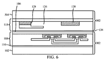
図3は、第1の絶縁層106の第1の側108をシート102に対向させ、反転し、第1の接着剤層116によってシート102に接合された、第1のストックSOIウエハ202を示し、図4は、たとえば、化学機械研磨(CMP)または他の所望の量の第1のシリコン処理層204を選択的に除去する適切なプロセスにより、第1のシリコン処理層204の除去によって形成された第1の構成部品302を示す。図5は、上に第2の絶縁層120および第2の回路層126が形成された第2のシリコン基板または処理層504を備える、第2のストックSOIウエハ502を示す。図6は、反転させ、第1の構成部品302に取り付け、第2のストックSOIウエハ502の第2の回路層126を第2の接着剤層134によって第1の絶縁層106に接合した、第2のストックSOIウエハ502を示す。図7は、第2のストックSOIウエハ502と第1の構成部品302との組合せを備え、第2のストックSOIウエハ502の第2のシリコン処理層504をCMPまたは他の適切なプロセスによって除去した、第2の構成部品702を示す。ビア136も、第2の構成部品702内に形成され、金属接点140および他のバックエンドオブザライン(BEOL)の構成部品(受動部品、MEMS、センサおよびその他を含む)の追加により、図1のチップセット100がもたらされる。
FIG. 3 shows the first
図8は、第1の実施形態に共通の要素が同じ参照符号で識別される、別の一実施形態を示す。図8は、シート102と、第1のSOIウエハ104と、第2のSOIウエハ118とを含み、第1のSOIウエハ104および第2のSOIウエハ118は、第3のSOIウエハ802によって離隔されている、第2のチップセット800を示す。第3のSOIウエハ802は、第1の側806および第2の側808を有する第3の基板層または絶縁層804と、第3の絶縁層804の第1の側806上に複数の回路素子を備える第3の回路層810とを備えており、回路素子はアナログ回路814および/またはRF構成部品816を含むことができる。第3のSOIウエハ802は、第3のSOIウエハ802の第1の側806が第1のSOIウエハ104の第2の側110に対向するように、第2の接着剤層818により第1のSOIウエハ104の第2の側110に取り付けられる。第2のSOIウエハ118は、第2のSOIウエハ118の第1の側が第3のSOIウエハ802の第2の側808に対向するように、第3の接着剤層820によって第3のSOIウエハ802の第2の側808に取り付けられる。第1のSOIウエハ104、第2のSOIウエハ118および第3のSOIウエハ802の3つすべてが、実質的に同じ表面積を有する。ビア822が、第1の回路層112、第2の回路層126および第3の回路層810の回路構成部品を接続し、金属接点140が、第2のチップセット800の外側の素子との接続部を提供する。この構成により、アナログ回路814および/またはRF構成部品816をデジタル回路素子114およびコンデンサ132などの受動部品と同じチップセット内に含めることが可能になり、小型パッケージ内で多くの従来の機能を実施する垂直に集積されたチップセットが提供される。
FIG. 8 shows another embodiment in which elements common to the first embodiment are identified with the same reference numerals. FIG. 8 includes a
シート102は、ガラス、サファイアまたは石英を備えるとして説明されているが、シート102にガラスを使用することは、状況によってとりわけ有益である。まず、ガラスは、一般にサファイアまたは石英より費用が安い。次に、ガラスは、サファイアより誘電率がずっと低く、それによって、基板からの寄生容量が著しく低減する。最後に、ガラスのウエハ/パネルのサイズは、サファイアおよび石英よりずっと大きくすることができ、これにより、より大規模な量産およびより低い単価が可能になる。
Although the
開示された本実施形態のチップセットは、1つまたは複数の半導体ダイに集積することができ、セットトップボックス、音楽プレーヤ、ビデオプレーヤ、娯楽ユニット、ナビゲーションデバイス、通信デバイス、携帯情報端末(PDA)、固定ロケーションデータユニット、およびコンピュータなどのデバイスに統合することができる。 The disclosed chipset of this embodiment can be integrated on one or more semiconductor dies, and can be set-top boxes, music players, video players, entertainment units, navigation devices, communication devices, personal digital assistants (PDAs) Can be integrated into devices such as fixed location data units, and computers.
本明細書で開示された実施形態に関連して説明した方法、シーケンス、および/またはアルゴリズムは、直接ハードウェアにおいて、プロセッサによって実行されるソフトウェアモジュールにおいて、またはこの2つの組合せにおいて実施することができる。ソフトウェアモジュールは、RAMメモリ、フラッシュメモリ、ROMメモリ、EPROMメモリ、EEPROMメモリ、レジスタ、ハードディスク、リムーバブルディスク、CD−ROM、または当技術分野で周知の他の任意の形の記憶媒体に常駐することができる。例示的な記憶媒体は、プロセッサが記憶媒体から情報を読み取り、および記憶媒体に情報を書き込むことができるように、プロセッサに結合される。あるいは、記憶媒体は、プロセッサと一体にすることができる。 The methods, sequences, and / or algorithms described in connection with the embodiments disclosed herein may be implemented directly in hardware, in software modules executed by a processor, or in a combination of the two. . A software module may reside in RAM memory, flash memory, ROM memory, EPROM memory, EEPROM memory, registers, hard disk, a removable disk, a CD-ROM, or any other form of storage medium known in the art. it can. An exemplary storage medium is coupled to the processor such that the processor can read information from, and write information to, the storage medium. In the alternative, the storage medium may be integral to the processor.
前述の開示により、本発明の例示的な実施形態が示されているが、添付の特許請求の範囲に定義されるように、本発明の範囲を逸脱することなく、本明細書において様々な変更および修正を加えることができることに留意されたい。本明細書に説明する本発明の諸実施形態による方法の特許請求の範囲の諸機能、諸ステップ、および/または諸動作は、任意の特定の順序で実施する必要はない。さらに、本発明の諸要素は、単数で説明しまたは特許請求することができるが、単数への限定が明示的に記述されていない限り、複数が企図されている。 While the foregoing disclosure sets forth exemplary embodiments of the present invention, various changes may be made herein without departing from the scope of the invention as defined in the appended claims. Note that and modifications can be made. The features, steps, and / or actions of the claims of the method according to embodiments of the invention described herein need not be performed in any particular order. Further, although elements of the invention may be described or claimed in the singular, the plural is contemplated unless limitation to the singular is explicitly stated.
100 チップセット
102 シート
104 第1のシリコンオンインシュレータ(SOI)ウエハ
106 第1の基板層または第1の絶縁層
108 第1の側
110 第2の側
112 第1の回路層
114 CMOSトランジスタ(デジタル回路素子)
116 第1の接着剤層
118 第2のSOIウエハ
120 第2の基板層または第2の絶縁層
122 第1の側
124 第2の側
126 第2の回路層
128 抵抗器
132 コンデンサ
133 誘導子
134 第2の接着剤層
136 ビア
138 MEMSデバイス
140 金属接点
202 第1のストックSOIウエハ
204 第1のシリコン基板または処理層
302 第1の構成部品
502 第2のストックSOIウエハ
504 第2のシリコン基板または処理層
702 第2の構成部品
800 第2のチップセット
802 第3のSOIウエハ
804 第3の基板層または絶縁層
806 第1の側
808 第2の側
810 第3の回路層
814 アナログ回路
816 RF構成部品
818 第2の接着剤層
820 第3の接着剤層
822 ビア
100
116 First
Claims (23)
第1の絶縁層及び前記第1の絶縁層の第1の側上に形成された少なくとも1つの第1の回路層を備えた第1のシリコンオンインシュレータ(SOI)であって、前記少なくとも1つの第1の回路層が前記第1の絶縁層と前記シートとの間に配置されるように、前記シートに接合される第1のSOIと、
前記シートと前記第1のSOIとの間に配される接着剤層であって、前記第1のSOIの第1の回路層が前記接着剤層を介して前記シートに接合されるようになる接着剤層と、
第2の絶縁層及び少なくとも1つの第2の回路層を備えた第2のSOIであって、前記少なくとも1つの第2の回路層が、前記第2の絶縁層の第1の側上に形成される少なくとも1つの第1の受動回路要素と、前記第2の絶縁層の第2の側上に形成される少なくとも1つの第2の受動回路要素と、を備え、前記少なくとも1つの第1の受動回路要素が、前記第2の絶縁層と前記第1の絶縁層との間に配置され、前記第1の絶縁層の第2の側が、前記少なくとも1つの第2の回路層に結合されるように、前記第1の絶縁層に接続される、第2のSOIと、
を備えるチップセットであって、
前記少なくとも1つの第1の回路層が、複数のCMOSトランジスタを備え、
前記少なくとも1つの第2の回路層が、受動構成部品およびMEMS素子のうちの少なくとも1つを備えるまたは支持する、チップセット。 Glass, quartz or sapphire sheets,
A first silicon-on-insulator (SOI) comprising a first insulating layer and at least one first circuit layer formed on a first side of the first insulating layer , the at least one A first SOI bonded to the sheet such that a first circuit layer is disposed between the first insulating layer and the sheet;
An adhesive layer disposed between the sheet and the first SOI, wherein the first circuit layer of the first SOI is bonded to the sheet via the adhesive layer. An adhesive layer;
A second SOI comprising a second insulating layer and at least one second circuit layer, wherein the at least one second circuit layer is formed on a first side of the second insulating layer At least one first passive circuit element and at least one second passive circuit element formed on a second side of the second insulating layer, the at least one first A passive circuit element is disposed between the second insulating layer and the first insulating layer, and a second side of the first insulating layer is coupled to the at least one second circuit layer. A second SOI connected to the first insulating layer ;
A chipset comprising:
The at least one first circuit layer comprises a plurality of CMOS transistors;
The chipset, wherein the at least one second circuit layer comprises or supports at least one of a passive component and a MEMS element.
前記少なくとも1つの第2の回路層が、少なくとも1つの受動構成部品またはMEMS素子を備え又は支持し、
前記第1のSOIが、前記シートに直接接合され、
前記第2のSOIが、前記第1の絶縁層に直接接合される、請求項1に記載のチップセット。 The at least one first circuit layer comprises a plurality of complementary MOS (CMOS) transistors;
The at least one second circuit layer comprises or supports at least one passive component or MEMS element;
The first SOI is directly bonded to the sheet;
The chipset according to claim 1 , wherein the second SOI is directly bonded to the first insulating layer.
第1の絶縁層手段及び前記第1の絶縁層手段の第1の側上に形成される、信号を処理するための少なくとも1つの第1の回路手段を備えた第1のシリコンオンインシュレータ(SOI)であって、前記少なくとも1つの第1の回路手段が前記第1の絶縁層手段と前記絶縁体シート手段との間に配置されるように、前記絶縁体シート手段に接合される、第1のSOIと、
前記絶縁体シート手段と前記第1のSOIとの間に配される接着剤層であって、前記第1のSOIの第1の回路手段が前記接着剤層を介して前記絶縁体シート手段に接合されるようになる接着剤層と、
第2の絶縁層手段及び信号を処理するための少なくとも1つの第2の回路手段を備えた第2のSOIであって、前記少なくとも1つの第2の回路手段が、前記第2の絶縁層手段の第1の側上に形成される少なくとも1つの第1の受動回路要素と、前記第2の絶縁層手段の第2の側上に形成される少なくとも1つの第2の受動回路要素と、を備え、前記少なくとも1つの第1の受動回路要素が、前記第2の絶縁層手段と前記第1の絶縁層手段との間に配置され、前記第1の絶縁層手段の第2の側が、前記少なくとも1つの第2の回路手段に結合されるように、前記第1の絶縁層手段に接続される、第2のSOIと、
を備えるチップセットであって、
前記少なくとも1つの第1の回路手段が、複数のCMOSトランジスタを備え、
前記少なくとも1つの第2の回路手段が、受動回路素子と、微小電気機械システム(MEMS)素子と、センサのうちの少なくとも1つを備えるまたは支持する、チップセット。 Insulator sheet means for supporting a wafer, comprising an insulating sheet means comprising a glass sheet, a quartz sheet or a sapphire sheet ;
A first silicon-on-insulator (SOI) comprising a first insulating layer means and at least one first circuit means for processing a signal formed on a first side of the first insulating layer means . ) Wherein the at least one first circuit means is joined to the insulator sheet means such that the at least one first circuit means is disposed between the first insulating layer means and the insulator sheet means. With SOI ,
An adhesive layer disposed between the insulator sheet means and the first SOI, wherein the first circuit means of the first SOI is connected to the insulator sheet means via the adhesive layer. An adhesive layer to be joined,
A second SOI comprising a second insulating layer means and at least one second circuit means for processing a signal, wherein the at least one second circuit means comprises the second insulating layer means At least one first passive circuit element formed on the first side of the second insulating layer means and at least one second passive circuit element formed on the second side of the second insulating layer means. The at least one first passive circuit element is disposed between the second insulating layer means and the first insulating layer means, and a second side of the first insulating layer means is the A second SOI connected to the first insulating layer means to be coupled to at least one second circuit means ;
A chipset comprising:
The at least one first circuit means comprises a plurality of CMOS transistors;
A chipset, wherein the at least one second circuit means comprises or supports at least one of a passive circuit element, a microelectromechanical system (MEMS) element, and a sensor.
前記少なくとも1つの第2の回路手段が、少なくとも1つの受動構成部品または少なくとも1つのMEMS素子を備えまたは支持し、
前記第1のSOIが、前記絶縁体シート手段に直接接合され、
前記第2のSOIが、前記第1の絶縁層手段に直接接合される、
請求項15に記載のチップセット。 The at least one first circuit means comprises a plurality of CMOS transistors;
Said at least one second circuit means comprises or supports at least one passive component or at least one MEMS element;
The first SOI is directly bonded to the insulator sheet means;
The second SOI is directly bonded to the first insulating layer means ;
The chip set according to claim 15 .
前記少なくとも1つの第2の回路層が、少なくとも1つの高Q受動部品を備える、請求項1に記載のチップセット。The chipset of claim 1, wherein the at least one second circuit layer comprises at least one high-Q passive component.
前記少なくとも1つの第2の回路層が、少なくとも1つの半導体バラクタを備える、請求項1に記載のチップセット。The chipset of claim 1, wherein the at least one second circuit layer comprises at least one semiconductor varactor.
前記少なくとも1つの第2の回路層が、少なくとも1つのMEMSベースの同調可能なコンデンサを備える、請求項1に記載のチップセット。The chipset of claim 1, wherein the at least one second circuit layer comprises at least one MEMS-based tunable capacitor.
前記少なくとも1つの第2の回路層が、少なくとも1つの高性能無線周波数(RF)スイッチを備える、請求項1に記載のチップセット。The chipset of claim 1, wherein the at least one second circuit layer comprises at least one high performance radio frequency (RF) switch.
Applications Claiming Priority (5)
| Application Number | Priority Date | Filing Date | Title |
|---|---|---|---|
| US201161560471P | 2011-11-16 | 2011-11-16 | |
| US61/560,471 | 2011-11-16 | ||
| US13/356,717 | 2012-01-24 | ||
| US13/356,717 US9496255B2 (en) | 2011-11-16 | 2012-01-24 | Stacked CMOS chipset having an insulating layer and a secondary layer and method of forming same |
| PCT/US2012/065644 WO2013075007A1 (en) | 2011-11-16 | 2012-11-16 | Stacked chipset having an insulating layer and a secondary layer and method of forming same |
Related Child Applications (1)
| Application Number | Title | Priority Date | Filing Date |
|---|---|---|---|
| JP2016095168A Division JP6099794B2 (en) | 2011-11-16 | 2016-05-11 | Stacked chipset having insulating layer and second layer and method for forming the same |
Publications (2)
| Publication Number | Publication Date |
|---|---|
| JP2015503228A JP2015503228A (en) | 2015-01-29 |
| JP5937225B2 true JP5937225B2 (en) | 2016-06-22 |
Family
ID=48280458
Family Applications (2)
| Application Number | Title | Priority Date | Filing Date |
|---|---|---|---|
| JP2014542512A Active JP5937225B2 (en) | 2011-11-16 | 2012-11-16 | Stacked chipset having insulating layer and second layer and method for forming the same |
| JP2016095168A Expired - Fee Related JP6099794B2 (en) | 2011-11-16 | 2016-05-11 | Stacked chipset having insulating layer and second layer and method for forming the same |
Family Applications After (1)
| Application Number | Title | Priority Date | Filing Date |
|---|---|---|---|
| JP2016095168A Expired - Fee Related JP6099794B2 (en) | 2011-11-16 | 2016-05-11 | Stacked chipset having insulating layer and second layer and method for forming the same |
Country Status (7)
| Country | Link |
|---|---|
| US (1) | US9496255B2 (en) |
| EP (1) | EP2780942A1 (en) |
| JP (2) | JP5937225B2 (en) |
| KR (2) | KR101759689B1 (en) |
| CN (1) | CN104054175B (en) |
| IN (1) | IN2014MN01027A (en) |
| WO (1) | WO2013075007A1 (en) |
Families Citing this family (48)
| Publication number | Priority date | Publication date | Assignee | Title |
|---|---|---|---|---|
| CN104058363B (en) * | 2013-03-22 | 2016-01-20 | 上海丽恒光微电子科技有限公司 | Based on the display unit and forming method thereof of MEMS transmissive light valve |
| US9418985B2 (en) | 2013-07-16 | 2016-08-16 | Qualcomm Incorporated | Complete system-on-chip (SOC) using monolithic three dimensional (3D) integrated circuit (IC) (3DIC) technology |
| US9032353B2 (en) | 2013-10-10 | 2015-05-12 | Taiwan Semiconductor Manufacturing Co., Ltd. | Method and system for three-dimensional layout design of integrated circuit elements in stacked CMOS |
| US9257407B2 (en) * | 2013-10-28 | 2016-02-09 | Qualcomm Incorporated | Heterogeneous channel material integration into wafer |
| US9443758B2 (en) * | 2013-12-11 | 2016-09-13 | Taiwan Semiconductor Manufacturing Co., Ltd. | Connecting techniques for stacked CMOS devices |
| US10079170B2 (en) | 2014-01-23 | 2018-09-18 | Globalwafers Co., Ltd. | High resistivity SOI wafers and a method of manufacturing thereof |
| US9786613B2 (en) * | 2014-08-07 | 2017-10-10 | Qualcomm Incorporated | EMI shield for high frequency layer transferred devices |
| US20160043108A1 (en) * | 2014-08-07 | 2016-02-11 | Silanna Semiconductor U.S.A., Inc. | Semiconductor Structure with Multiple Active Layers in an SOI Wafer |
| US9899499B2 (en) | 2014-09-04 | 2018-02-20 | Sunedison Semiconductor Limited (Uen201334164H) | High resistivity silicon-on-insulator wafer manufacturing method for reducing substrate loss |
| US10224233B2 (en) | 2014-11-18 | 2019-03-05 | Globalwafers Co., Ltd. | High resistivity silicon-on-insulator substrate comprising a charge trapping layer formed by He-N2 co-implantation |
| JP6650463B2 (en) | 2014-11-18 | 2020-02-19 | グローバルウェーハズ カンパニー リミテッドGlobalWafers Co.,Ltd. | Method of manufacturing high resistivity semiconductor-on-insulator wafer with charge trapping layer |
| EP3573094B1 (en) | 2014-11-18 | 2023-01-04 | GlobalWafers Co., Ltd. | High resistivity semiconductor-on-insulator wafer and a method of manufacturing |
| WO2016081363A1 (en) * | 2014-11-18 | 2016-05-26 | Sunedison Semiconductor Limited | A system-on-chip on a semiconductor-on-insulator wafer and a method of manufacturing |
| EP4120320A1 (en) | 2015-03-03 | 2023-01-18 | GlobalWafers Co., Ltd. | Charge trapping polycrystalline silicon films on silicon substrates with controllable film stress |
| JP6637515B2 (en) | 2015-03-17 | 2020-01-29 | グローバルウェーハズ カンパニー リミテッドGlobalWafers Co.,Ltd. | Thermally stable charge trapping layer for use in the fabrication of semiconductor-on-insulator structures |
| US9881832B2 (en) | 2015-03-17 | 2018-01-30 | Sunedison Semiconductor Limited (Uen201334164H) | Handle substrate for use in manufacture of semiconductor-on-insulator structure and method of manufacturing thereof |
| US10304722B2 (en) | 2015-06-01 | 2019-05-28 | Globalwafers Co., Ltd. | Method of manufacturing semiconductor-on-insulator |
| US10332782B2 (en) | 2015-06-01 | 2019-06-25 | Globalwafers Co., Ltd. | Method of manufacturing silicon germanium-on-insulator |
| US20160379943A1 (en) * | 2015-06-25 | 2016-12-29 | Skyworks Solutions, Inc. | Method and apparatus for high performance passive-active circuit integration |
| US20170033135A1 (en) * | 2015-07-28 | 2017-02-02 | Skyworks Solutions, Inc. | Integrated passive device on soi substrate |
| US9768109B2 (en) * | 2015-09-22 | 2017-09-19 | Qualcomm Incorporated | Integrated circuits (ICS) on a glass substrate |
| JP6585978B2 (en) | 2015-09-24 | 2019-10-02 | ラピスセミコンダクタ株式会社 | Semiconductor device and manufacturing method of semiconductor device |
| CN108780776B (en) | 2015-11-20 | 2023-09-29 | 环球晶圆股份有限公司 | Manufacturing method for flattening semiconductor surface |
| US10256863B2 (en) * | 2016-01-11 | 2019-04-09 | Qualcomm Incorporated | Monolithic integration of antenna switch and diplexer |
| US9831115B2 (en) | 2016-02-19 | 2017-11-28 | Sunedison Semiconductor Limited (Uen201334164H) | Process flow for manufacturing semiconductor on insulator structures in parallel |
| WO2017142704A1 (en) | 2016-02-19 | 2017-08-24 | Sunedison Semiconductor Limited | High resistivity silicon-on-insulator substrate comprising a charge trapping layer formed on a substrate with a rough surface |
| US10622247B2 (en) | 2016-02-19 | 2020-04-14 | Globalwafers Co., Ltd. | Semiconductor on insulator structure comprising a buried high resistivity layer |
| US10573550B2 (en) | 2016-03-07 | 2020-02-25 | Globalwafers Co., Ltd. | Semiconductor on insulator structure comprising a plasma oxide layer and method of manufacture thereof |
| WO2017155804A1 (en) | 2016-03-07 | 2017-09-14 | Sunedison Semiconductor Limited | Method of manufacturing a semiconductor on insulator structure by a pressurized bond treatment |
| EP3427293B1 (en) | 2016-03-07 | 2021-05-05 | Globalwafers Co., Ltd. | Semiconductor on insulator structure comprising a low temperature flowable oxide layer and method of manufacture thereof |
| US11114332B2 (en) | 2016-03-07 | 2021-09-07 | Globalwafers Co., Ltd. | Semiconductor on insulator structure comprising a plasma nitride layer and method of manufacture thereof |
| US11142844B2 (en) | 2016-06-08 | 2021-10-12 | Globalwafers Co., Ltd. | High resistivity single crystal silicon ingot and wafer having improved mechanical strength |
| US10269617B2 (en) | 2016-06-22 | 2019-04-23 | Globalwafers Co., Ltd. | High resistivity silicon-on-insulator substrate comprising an isolation region |
| US20180068886A1 (en) * | 2016-09-02 | 2018-03-08 | Qualcomm Incorporated | Porous semiconductor layer transfer for an integrated circuit structure |
| US9812580B1 (en) * | 2016-09-06 | 2017-11-07 | Qualcomm Incorporated | Deep trench active device with backside body contact |
| EP4057326A1 (en) | 2016-10-26 | 2022-09-14 | GlobalWafers Co., Ltd. | High resistivity silicon-on-insulator substrate having enhanced charge trapping efficiency |
| EP3549162B1 (en) | 2016-12-05 | 2022-02-02 | GlobalWafers Co., Ltd. | High resistivity silicon-on-insulator structure and method of manufacture thereof |
| EP3653761B1 (en) | 2016-12-28 | 2024-02-28 | Sunedison Semiconductor Limited | Silicon wafers with intrinsic gettering and gate oxide integrity yield |
| JP6881066B2 (en) * | 2017-06-19 | 2021-06-02 | 大日本印刷株式会社 | Manufacturing method of through silicon via substrate and through silicon via substrate |
| JP7034186B2 (en) | 2017-07-14 | 2022-03-11 | サンエディソン・セミコンダクター・リミテッド | Manufacturing method of semiconductor structure on insulator |
| WO2019209492A1 (en) | 2018-04-27 | 2019-10-31 | Globalwafers Co., Ltd. | Light assisted platelet formation facilitating layer transfer from a semiconductor donor substrate |
| JP2019212729A (en) * | 2018-06-04 | 2019-12-12 | ルネサスエレクトロニクス株式会社 | Semiconductor device and method for manufacturing semiconductor device |
| CN112262467A (en) | 2018-06-08 | 2021-01-22 | 环球晶圆股份有限公司 | Method for transferring thin silicon layers |
| FR3091004B1 (en) * | 2018-12-24 | 2020-12-04 | Soitec Silicon On Insulator | SEMICONDUCTOR TYPE STRUCTURE FOR DIGITAL AND RADIO FREQUENCY APPLICATIONS |
| EP3675168A1 (en) * | 2018-12-24 | 2020-07-01 | IMEC vzw | 3d power semiconductor device and system |
| JP2020141090A (en) * | 2019-03-01 | 2020-09-03 | ソニーセミコンダクタソリューションズ株式会社 | Capacitive element, semiconductor element substrate, and electronic device |
| KR20220008093A (en) | 2020-07-13 | 2022-01-20 | 삼성전자주식회사 | Semiconductor package and method of manufacturing the semiconductor package |
| CN114122134B (en) * | 2020-09-01 | 2023-12-22 | 苏州华太电子技术股份有限公司 | Radio frequency LDMOS integrated device |
Family Cites Families (20)
| Publication number | Priority date | Publication date | Assignee | Title |
|---|---|---|---|---|
| JP2001102523A (en) | 1999-09-28 | 2001-04-13 | Sony Corp | Thin-film device and manufacturing method therefor |
| US6399997B1 (en) | 2000-08-01 | 2002-06-04 | Megic Corporation | High performance system-on-chip using post passivation process and glass substrates |
| JP4244120B2 (en) | 2001-06-20 | 2009-03-25 | 株式会社半導体エネルギー研究所 | Light emitting device and manufacturing method thereof |
| TW548860B (en) | 2001-06-20 | 2003-08-21 | Semiconductor Energy Lab | Light emitting device and method of manufacturing the same |
| US7402897B2 (en) | 2002-08-08 | 2008-07-22 | Elm Technology Corporation | Vertical system integration |
| JP2004165269A (en) | 2002-11-11 | 2004-06-10 | Canon Inc | Laminated semiconductor device |
| JP2004349513A (en) | 2003-05-22 | 2004-12-09 | Seiko Epson Corp | Thin film circuit device, its manufacturing method, electrooptic device, and electronic equipment |
| CN102290425B (en) * | 2004-08-20 | 2014-04-02 | Kamiyacho知识产权控股公司 | Method of fabricating semiconductor device having three-dimensional stacked structure |
| US7179719B2 (en) | 2004-09-28 | 2007-02-20 | Sharp Laboratories Of America, Inc. | System and method for hydrogen exfoliation |
| US20070207592A1 (en) | 2006-03-03 | 2007-09-06 | Lu James J | Wafer bonding of damascene-patterned metal/adhesive redistribution layers |
| US7408798B2 (en) | 2006-03-31 | 2008-08-05 | International Business Machines Corporation | 3-dimensional integrated circuit architecture, structure and method for fabrication thereof |
| US20080128901A1 (en) * | 2006-11-30 | 2008-06-05 | Peter Zurcher | Micro-electro-mechanical systems device and integrated circuit device integrated in a three-dimensional semiconductor structure |
| US20080149832A1 (en) * | 2006-12-20 | 2008-06-26 | Miguel Zorn | Scanning Probe Microscope, Nanomanipulator with Nanospool, Motor, nucleotide cassette and Gaming application |
| JP2009067098A (en) | 2007-09-10 | 2009-04-02 | Harison Toshiba Lighting Corp | Lighting system |
| JP2009267098A (en) * | 2008-04-25 | 2009-11-12 | Denso Corp | Semiconductor apparatus and method of manufacturing the same |
| US7943428B2 (en) * | 2008-12-24 | 2011-05-17 | International Business Machines Corporation | Bonded semiconductor substrate including a cooling mechanism |
| US7943423B2 (en) | 2009-03-10 | 2011-05-17 | Infineon Technologies Ag | Reconfigured wafer alignment |
| US9406561B2 (en) | 2009-04-20 | 2016-08-02 | International Business Machines Corporation | Three dimensional integrated circuit integration using dielectric bonding first and through via formation last |
| JP2011029609A (en) * | 2009-06-26 | 2011-02-10 | Semiconductor Energy Lab Co Ltd | Method for manufacturing soi substrate, and soi substrate |
| US9076664B2 (en) * | 2011-10-07 | 2015-07-07 | Freescale Semiconductor, Inc. | Stacked semiconductor die with continuous conductive vias |
-
2012
- 2012-01-24 US US13/356,717 patent/US9496255B2/en active Active
- 2012-11-16 JP JP2014542512A patent/JP5937225B2/en active Active
- 2012-11-16 EP EP12799674.2A patent/EP2780942A1/en not_active Ceased
- 2012-11-16 KR KR1020167009373A patent/KR101759689B1/en active IP Right Grant
- 2012-11-16 CN CN201280067053.4A patent/CN104054175B/en active Active
- 2012-11-16 KR KR1020147016198A patent/KR20140100526A/en active Application Filing
- 2012-11-16 WO PCT/US2012/065644 patent/WO2013075007A1/en active Application Filing
- 2012-11-16 IN IN1027MUN2014 patent/IN2014MN01027A/en unknown
-
2016
- 2016-05-11 JP JP2016095168A patent/JP6099794B2/en not_active Expired - Fee Related
Also Published As
| Publication number | Publication date |
|---|---|
| JP2016174170A (en) | 2016-09-29 |
| KR101759689B1 (en) | 2017-07-19 |
| WO2013075007A1 (en) | 2013-05-23 |
| CN104054175A (en) | 2014-09-17 |
| US9496255B2 (en) | 2016-11-15 |
| JP6099794B2 (en) | 2017-03-22 |
| KR20140100526A (en) | 2014-08-14 |
| CN104054175B (en) | 2018-03-06 |
| JP2015503228A (en) | 2015-01-29 |
| US20130120951A1 (en) | 2013-05-16 |
| EP2780942A1 (en) | 2014-09-24 |
| IN2014MN01027A (en) | 2015-05-01 |
| KR20160044591A (en) | 2016-04-25 |
Similar Documents
| Publication | Publication Date | Title |
|---|---|---|
| JP6099794B2 (en) | Stacked chipset having insulating layer and second layer and method for forming the same | |
| CN110088891B (en) | Logic block layout using double-sided processing | |
| JP6856739B2 (en) | An integrated circuit having components on both sides of the selected substrate and its manufacturing method | |
| JP2016174170A5 (en) | ||
| US8148793B2 (en) | Three dimensional integrated passive device and method of fabrication | |
| EP3449503B1 (en) | Integrated radio frequency circuit structure | |
| TWI693676B (en) | Integrated passive device on soi substrate | |
| TWI756206B (en) | Tunable radio frequency systems using piezoelectric package-integrated switching devices | |
| US9061890B2 (en) | Methods of forming buried electromechanical structures coupled with device substrates and structures formed thereby | |
| JP2016526287A (en) | Adjustable diplexer and related components and methods in a three-dimensional (3D) integrated circuit (IC) (3DIC) | |
| US20190273116A1 (en) | Integrated acoustic filter on complementary metal oxide semiconductor (cmos) die | |
| JP2007000961A (en) | Semiconductor compound device and manufacturing method thereof | |
| JP5304398B2 (en) | Variable capacitance element | |
| KR20200057714A (en) | Bulk layer transfer processing by rear silicide | |
| WO2018044494A1 (en) | Porous semiconductor layer transfer for an integrated circuit structure | |
| US20220069193A1 (en) | Package comprising an integrated passive device configured as a cap for a filter | |
| JP2010135614A (en) | Variable capacitance element | |
| WO2018034756A1 (en) | Utilization of backside silicidation to form dual side contacted capacitor | |
| US20200168402A1 (en) | Microelectronic devices designed with package integrated variable capacitors having piezoelectric actuation |
Legal Events
| Date | Code | Title | Description |
|---|---|---|---|
| A131 | Notification of reasons for refusal |
Free format text: JAPANESE INTERMEDIATE CODE: A131 Effective date: 20150824 |
|
| A601 | Written request for extension of time |
Free format text: JAPANESE INTERMEDIATE CODE: A601 Effective date: 20151124 |
|
| A521 | Request for written amendment filed |
Free format text: JAPANESE INTERMEDIATE CODE: A523 Effective date: 20160224 |
|
| TRDD | Decision of grant or rejection written | ||
| A01 | Written decision to grant a patent or to grant a registration (utility model) |
Free format text: JAPANESE INTERMEDIATE CODE: A01 Effective date: 20160411 |
|
| A61 | First payment of annual fees (during grant procedure) |
Free format text: JAPANESE INTERMEDIATE CODE: A61 Effective date: 20160511 |
|
| R150 | Certificate of patent or registration of utility model |
Ref document number: 5937225 Country of ref document: JP Free format text: JAPANESE INTERMEDIATE CODE: R150 |
|
| R250 | Receipt of annual fees |
Free format text: JAPANESE INTERMEDIATE CODE: R250 |
|
| R250 | Receipt of annual fees |
Free format text: JAPANESE INTERMEDIATE CODE: R250 |
|
| R250 | Receipt of annual fees |
Free format text: JAPANESE INTERMEDIATE CODE: R250 |
|
| R250 | Receipt of annual fees |
Free format text: JAPANESE INTERMEDIATE CODE: R250 |
|
| R250 | Receipt of annual fees |
Free format text: JAPANESE INTERMEDIATE CODE: R250 |