KR20140090176A - Electroconductive sheet and touch panel - Google Patents
Electroconductive sheet and touch panel Download PDFInfo
- Publication number
- KR20140090176A KR20140090176A KR1020147011932A KR20147011932A KR20140090176A KR 20140090176 A KR20140090176 A KR 20140090176A KR 1020147011932 A KR1020147011932 A KR 1020147011932A KR 20147011932 A KR20147011932 A KR 20147011932A KR 20140090176 A KR20140090176 A KR 20140090176A
- Authority
- KR
- South Korea
- Prior art keywords
- electrode
- pattern
- conductive sheet
- electrode pattern
- conductive
- Prior art date
Links
Images


Classifications
-
- G—PHYSICS
- G06—COMPUTING; CALCULATING OR COUNTING
- G06F—ELECTRIC DIGITAL DATA PROCESSING
- G06F3/00—Input arrangements for transferring data to be processed into a form capable of being handled by the computer; Output arrangements for transferring data from processing unit to output unit, e.g. interface arrangements
- G06F3/01—Input arrangements or combined input and output arrangements for interaction between user and computer
- G06F3/03—Arrangements for converting the position or the displacement of a member into a coded form
- G06F3/041—Digitisers, e.g. for touch screens or touch pads, characterised by the transducing means
- G06F3/044—Digitisers, e.g. for touch screens or touch pads, characterised by the transducing means by capacitive means
- G06F3/0445—Digitisers, e.g. for touch screens or touch pads, characterised by the transducing means by capacitive means using two or more layers of sensing electrodes, e.g. using two layers of electrodes separated by a dielectric layer
-
- B—PERFORMING OPERATIONS; TRANSPORTING
- B32—LAYERED PRODUCTS
- B32B—LAYERED PRODUCTS, i.e. PRODUCTS BUILT-UP OF STRATA OF FLAT OR NON-FLAT, e.g. CELLULAR OR HONEYCOMB, FORM
- B32B15/00—Layered products comprising a layer of metal
- B32B15/14—Layered products comprising a layer of metal next to a fibrous or filamentary layer
-
- G—PHYSICS
- G06—COMPUTING; CALCULATING OR COUNTING
- G06F—ELECTRIC DIGITAL DATA PROCESSING
- G06F3/00—Input arrangements for transferring data to be processed into a form capable of being handled by the computer; Output arrangements for transferring data from processing unit to output unit, e.g. interface arrangements
- G06F3/01—Input arrangements or combined input and output arrangements for interaction between user and computer
- G06F3/03—Arrangements for converting the position or the displacement of a member into a coded form
- G06F3/041—Digitisers, e.g. for touch screens or touch pads, characterised by the transducing means
- G06F3/044—Digitisers, e.g. for touch screens or touch pads, characterised by the transducing means by capacitive means
- G06F3/0446—Digitisers, e.g. for touch screens or touch pads, characterised by the transducing means by capacitive means using a grid-like structure of electrodes in at least two directions, e.g. using row and column electrodes
-
- H—ELECTRICITY
- H05—ELECTRIC TECHNIQUES NOT OTHERWISE PROVIDED FOR
- H05K—PRINTED CIRCUITS; CASINGS OR CONSTRUCTIONAL DETAILS OF ELECTRIC APPARATUS; MANUFACTURE OF ASSEMBLAGES OF ELECTRICAL COMPONENTS
- H05K1/00—Printed circuits
- H05K1/02—Details
- H05K1/0274—Optical details, e.g. printed circuits comprising integral optical means
-
- H—ELECTRICITY
- H05—ELECTRIC TECHNIQUES NOT OTHERWISE PROVIDED FOR
- H05K—PRINTED CIRCUITS; CASINGS OR CONSTRUCTIONAL DETAILS OF ELECTRIC APPARATUS; MANUFACTURE OF ASSEMBLAGES OF ELECTRICAL COMPONENTS
- H05K1/00—Printed circuits
- H05K1/02—Details
- H05K1/0296—Conductive pattern lay-out details not covered by sub groups H05K1/02 - H05K1/0295
-
- G—PHYSICS
- G06—COMPUTING; CALCULATING OR COUNTING
- G06F—ELECTRIC DIGITAL DATA PROCESSING
- G06F2203/00—Indexing scheme relating to G06F3/00 - G06F3/048
- G06F2203/041—Indexing scheme relating to G06F3/041 - G06F3/045
- G06F2203/04103—Manufacturing, i.e. details related to manufacturing processes specially suited for touch sensitive devices
-
- G—PHYSICS
- G06—COMPUTING; CALCULATING OR COUNTING
- G06F—ELECTRIC DIGITAL DATA PROCESSING
- G06F2203/00—Indexing scheme relating to G06F3/00 - G06F3/048
- G06F2203/041—Indexing scheme relating to G06F3/041 - G06F3/045
- G06F2203/04111—Cross over in capacitive digitiser, i.e. details of structures for connecting electrodes of the sensing pattern where the connections cross each other, e.g. bridge structures comprising an insulating layer, or vias through substrate
-
- G—PHYSICS
- G06—COMPUTING; CALCULATING OR COUNTING
- G06F—ELECTRIC DIGITAL DATA PROCESSING
- G06F2203/00—Indexing scheme relating to G06F3/00 - G06F3/048
- G06F2203/041—Indexing scheme relating to G06F3/041 - G06F3/045
- G06F2203/04112—Electrode mesh in capacitive digitiser: electrode for touch sensing is formed of a mesh of very fine, normally metallic, interconnected lines that are almost invisible to see. This provides a quite large but transparent electrode surface, without need for ITO or similar transparent conductive material
-
- H—ELECTRICITY
- H05—ELECTRIC TECHNIQUES NOT OTHERWISE PROVIDED FOR
- H05K—PRINTED CIRCUITS; CASINGS OR CONSTRUCTIONAL DETAILS OF ELECTRIC APPARATUS; MANUFACTURE OF ASSEMBLAGES OF ELECTRICAL COMPONENTS
- H05K2201/00—Indexing scheme relating to printed circuits covered by H05K1/00
- H05K2201/09—Shape and layout
- H05K2201/09209—Shape and layout details of conductors
- H05K2201/09218—Conductive traces
- H05K2201/09245—Crossing layout
Abstract
센싱 영역의 전극 단자의 근방에 있어서 시인성을 해치지 않는 도전 시트 및 터치 패널이 제공된다. 금속 세선들을 사용하여 구성된 전극 패턴 (16A) (16B), 및 이 전극 패턴 (16A) (16B) 의 단부에 전기적으로 접속된 전극 단자 (60A) (60B) 를 갖는 도전 시트 (12A) (12B) 에 있어서, 전극 패턴 (16A) (16B) 의 투과율은 적어도 83 % 이며, 전극 패턴 (16A) (16B) 의 투과율을 a % 로서 표현할 때에, 전극 단자 (60A) (60B) 의 투과율은 (a-20) % 내지 (a-3) % 이다.There is provided a conductive sheet and a touch panel which do not impair the visibility in the vicinity of the electrode terminal in the sensing area. Conductive sheets 12A and 12B having electrode patterns 16A and 16B formed using metal thin wires and electrode terminals 60A and 60B electrically connected to ends of the electrode patterns 16A and 16B, The transmittance of the electrode terminals 16A and 16B is at least 83% and the transmittances of the electrode terminals 60A and 60B are expressed by a-% when the transmittance of the electrode patterns 16A and 16B is expressed as a% 20)% to (a-3)%.
Description
본 발명은 도전 시트 및 터치 패널에 관한 것이며, 예를 들어, 투영형 정전용량방식의 (projected capacitive) 터치 패널에 사용되는 도전 시트 및 터치 패널에 관한 것이다.The present invention relates to a conductive sheet and a touch panel, and more particularly, to a conductive sheet and a touch panel used in a projected capacitive touch panel, for example.
금속 세선을 사용한 투명 도전막에 대해서는, 예를 들어, 특허문헌 1 및 특허문헌 2 에 기재된 바와 같이 연구가 계속되고 있다.As for the transparent conductive film using metal thin wires, for example, researches as described in
최근, 터치 패널이 주목받고 있다. 터치 패널은 PDA (휴대 정보 단말) 및 휴대 전화와 같은 작은 사이즈를 갖는 디바이스들에 주로 적용되고 있지만, PC용 디스플레이와 같은 보다 큰 사이즈를 갖는 디바이스들에의 적용이 진행될 것으로 생각된다.Recently, a touch panel has attracted attention. Although the touch panel is mainly applied to devices having a small size such as a PDA (portable information terminal) and a mobile phone, it is thought that the application to a device having a larger size such as a display for a PC is going to proceed.
이와 같은 장래의 동향에 있어서, 종래의 전극은 ITO (산화 인듐 주석) 를 이용하고 있다. ITO 는, 저항이 크고, 적용 사이즈가 커짐에 따라, 전극들 간의 전류의 전달 속도가 느려지고, 응답 속도 (손가락을 접촉한 시간과 그 위치를 검출할 때의 시간 사이의 시간 기간) 가 느려진다는 문제가 있다.In such future trends, ITO (indium tin oxide) is used as a conventional electrode. As ITO has a large resistance and a large application size, the transfer speed of the current between the electrodes is slow, and the problem that the response speed (time period between the time of touching the finger and the time of detecting the position) .
그래서, 금속 세선으로 구성된 전극에 의해 표면 저항을 저하시키는 것이 고려된다. 금속 세선을 전극에 사용한 터치 패널로서는, 예를 들어, 특허문헌 3 내지 특허문헌 9 가 알려져 있다.Thus, it is considered that the surface resistance is lowered by the electrode composed of the metal thin wire. For example, Patent Documents 3 to 9 are known as touch panels using metal thin wires as electrodes.
그런데, 터치 패널의 센싱 전극은, 적어도 터치 영역에 금속 세선을 포함하는 전극 패턴 및 이 전극 패턴의 단부에 전기적으로 접속된 전극 단자를 갖는다. 전극 단자는, 높은 도전성을 갖기 위해 굵은 단자이다. 그리하여, 디스플레이와 터치 패널을 조합하여 작동시키는 경우에, 전극 단자는, 센싱 영역 (전극 패턴) 에서 디스플레이로부터 방출된 광을 차광한다. 따라서, 센싱 영역의 전극 단자 근방에 어두워진 부분이 나타나고, 디스플레이는 때때로 잘 보이지 않게 된다.The sensing electrode of the touch panel has at least an electrode pattern including metal thin wires in the touch region and an electrode terminal electrically connected to the end of the electrode pattern. The electrode terminal is a thick terminal for high conductivity. Thus, when the display and the touch panel are operated in combination, the electrode terminal shields light emitted from the display in the sensing area (electrode pattern). Therefore, a darkened portion appears near the electrode terminal of the sensing region, and the display sometimes becomes invisible.
본 발명은 이와 같은 과제를 고려하여 된 것이며, 센싱 영역의 전극 단자 근방에 있어서 시인성을 손상시키지 않는 도전 시트 및 터치 패널을 제공하는 것을 목적으로 한다.SUMMARY OF THE INVENTION It is an object of the present invention to provide a conductive sheet and a touch panel which do not deteriorate visibility in the vicinity of an electrode terminal of a sensing region.
본 발명에 따른 제 1 도전 시트는, 금속 세선으로 구성된 전극 패턴; 및 전극 패턴의 단부에 전기적으로 접속된 전극 단자를 포함하는 도전 시트이고, 전극 패턴의 투과율이 83 % 이상이며, 전극 패턴의 투과율을 a % 로 나타낼 때에, 전극 단자의 투과율은 (a-20) % 이상 (a-3) % 이하이다.A first conductive sheet according to the present invention includes: an electrode pattern composed of metal thin wires; And the electrode terminal electrically connected to the end portion of the electrode pattern. When the transmittance of the electrode pattern is 83% or more and the transmittance of the electrode pattern is expressed as a%, the transmittance of the electrode terminal is (a-20) % Or more and (a-3)% or less.
본 발명에 따른 다른 양태의 제 1 도전 시트는, 금속 세선으로 구성된 전극 패턴; 및 전극 패턴의 단부에 전기적으로 접속된 전극 단자를 포함하는 도전 시트이고, 전극 패턴의 개구율이 90 % 이상이며, 전극 패턴의 개구율을 b % 로 나타낼 때에, 전극 단자의 개구율은 (b-20) % 이상 (b-0.1) % 이하이다.A first conductive sheet according to another aspect of the present invention includes: an electrode pattern composed of metal thin wires; And an electrode terminal electrically connected to an end portion of the electrode pattern, wherein when the aperture ratio of the electrode pattern is 90% or more and the aperture ratio of the electrode pattern is b%, the aperture ratio of the electrode terminal is (b-20) % Or more and (b-0.1)% or less.
상기 기재된 본 발명에 따른 제 1 도전 시트에 있어서, 전극 단자는 금속 세선으로 구성된 격자들로 이루어진 메시 형상을 포함하고 금속 세선은 30 ㎛ 이하의 선폭을 가지며, 금속 세선은 불투명한 재료로 구성되는 것이 바람직하다.In the first conductive sheet according to the present invention described above, it is preferable that the electrode terminal include a mesh-like shape composed of grids composed of metal thin wires, the metal thin wire has a line width of 30 mu m or less, and the metal thin wire is made of an opaque material desirable.
본 발명에 따른 제 1 터치 패널은, 센싱 영역에 제공되고 금속 세선으로 구성된 전극 패턴; 및 센싱 영역의 외측에 제공되고 전극 패턴의 단부에 전기적으로 접속된 전극 단자를 포함하는 도전 시트를 갖는 터치 패널이고, 전극 패턴의 투과율이 83 % 이상이며, 전극 패턴의 투과율을 a % 로 나타낼 때에, 전극 단자의 투과율은 (a-20) % 이상 (a-3) % 이하이다.A first touch panel according to the present invention includes: an electrode pattern provided in a sensing region and composed of a metal thin wire; And a conductive sheet provided on an outer side of the sensing region and electrically connected to an end of the electrode pattern, wherein when the transmittance of the electrode pattern is 83% or more and the transmittance of the electrode pattern is expressed as a% , And the transmittance of the electrode terminal is (a-20)% or more and (a-3)% or less.
본 발명에 따른 다른 양태의 제 1 터치 패널은, 센싱 영역에 제공되고 금속 세선으로 구성된 전극 패턴; 및 센싱 영역의 외측에 제공되고 전극 패턴의 단부에 전기적으로 접속된 전극 단자를 포함하는 도전 시트를 갖는 터치 패널이고, 전극 패턴의 개구율이 90 % 이상이며, 전극 패턴의 개구율을 b % 로 나타낼 때에, 전극 단자의 개구율은 (b-20) % 이상 (b-0.1) % 이하이다.A first touch panel according to another aspect of the present invention includes: an electrode pattern provided in a sensing area and composed of a metal thin wire; And a conductive sheet provided on an outer side of the sensing region and electrically connected to an end portion of the electrode pattern, wherein when the aperture ratio of the electrode pattern is 90% or more and the aperture ratio of the electrode pattern is b% , And the opening ratio of the electrode terminal is (b-20)% or more and (b-0.1)% or less.
본 발명에 따른 제 2 도전 시트는, 금속 세선으로 구성된 전극 패턴; 및 전극 패턴의 단부에 전기적으로 접속된 전극 단자를 포함하는 도전 시트이고, 전극 단자는, 금속 세선으로 구성된 프레임 형상을 포함한다.The second conductive sheet according to the present invention includes: an electrode pattern composed of a metal thin wire; And an electrode terminal electrically connected to an end portion of the electrode pattern, and the electrode terminal includes a frame shape composed of metal thin wires.
본 발명에 따른 제 2 도전 시트에 있어서, 바람직하게는, 전극 패턴의 세선의 선폭을 a (㎛) 로 나타낼 때에, 전극 단자의 프레임 형상의 선폭 b (㎛) 는 b ≥ 2a 또는 b ≥ a+5 (㎛) 를 만족한다. 전극 패턴의 세선의 선폭 a (㎛) 는 30 ㎛ 이하인 것이 바람직하다.In the second conductive sheet according to the present invention, preferably, when the line width of the fine line of the electrode pattern is represented by a (占 퐉), the line width b (占 퐉) of the frame shape of the electrode terminal is b? 2a or b? A + 5 (占 퐉). The line width a (mu m) of the fine lines of the electrode pattern is preferably 30 mu m or less.
본 발명에 따른 제 2 도전 시트는, 전극 단자의 금속 세선으로 구성된 프레임 형상 내에 제공된 메시 형상으로서, 금속 세선으로 구성된 격자들로 이루어진, 상기 메시 형상을 더 포함하는 것이 바람직하다.Preferably, the second conductive sheet according to the present invention further comprises the mesh shape, which is a mesh shape provided in a frame shape composed of metal thin wires of the electrode terminal, and is made of grids made of metal thin wires.
본 발명에 따른 제 2 터치 패널은, 센싱 영역에 제공되고 금속 세선으로 구성된 전극 패턴; 및 센싱 영역의 외측에 제공되고 전극 패턴의 단부에 전기적으로 접속된 전극 단자를 포함하는 도전 시트를 갖는 터치 패널이고, 전극 단자는, 금속 세선으로 구성된 프레임 형상을 포함한다.A second touch panel according to the present invention includes: an electrode pattern provided in a sensing region and composed of a metal thin wire; And a conductive sheet provided on the outside of the sensing region and including an electrode terminal electrically connected to an end portion of the electrode pattern, wherein the electrode terminal includes a frame shape composed of metal thin wires.
본 발명에 따른 제 3 도전 시트는, 금속 세선으로 구성된 전극 패턴; 및 전극 패턴의 단부에 전기적으로 접속된 전극 단자를 포함하는 도전 시트이고, 전극 단자는, 금속 세선으로 구성된 격자들로 이루어진 메시 형상을 포함한다.The third conductive sheet according to the present invention comprises: an electrode pattern composed of metal thin wires; And an electrode terminal electrically connected to an end of the electrode pattern, wherein the electrode terminal includes a mesh shape of grids composed of metal thin wires.
본 발명에 따른 제 3 도전 시트에 있어서, 전극 패턴은 격자들로 이루어진 메시 형상을 가지며, 전극 단자의 격자들로 이루어진 메시 형상의 피치는, 전극 패턴의 격자들로 이루어진 메시 형상의 피치보다 더 조밀한 것이 바람직하다. 전극 단자의 격자들로 이루어진 메시 형상의 피치는, 전극 패턴의 격자들로 이루어진 메시 형상의 피치의 3/4 이하인 것이 바람직하고, 전극 패턴의 격자들로 이루어진 메시 형상의 피치의 2/3 이하인 것이 보다 바람직하고, 전극 패턴의 격자들로 이루어진 메시 형상의 피치의 1/2 이하인 것이 더욱 더 바람직하다. 전극 단자의 메시 형상의 특정 피치는 50 ㎛ 이상 300 ㎛ 이하이고, 50 ㎛ 이상 250 ㎛ 이하인 것이 보다 바람직하다.In the third conductive sheet according to the present invention, the electrode pattern has a mesh shape composed of grids, and the mesh-like pitch composed of grids of electrode terminals is denser than the mesh-shaped pitch composed of grids of electrode patterns . The pitch of the mesh-shaped gratings of the electrode terminals is preferably 3/4 or less of the pitch of the mesh-shaped gratings, and is preferably 2/3 or less of the pitch of the mesh- And more preferably not more than 1/2 of the pitch of the mesh-like shape of the lattice of the electrode pattern. It is more preferable that the specific pitch of the mesh shape of the electrode terminal is 50 mu m or more and 300 mu m or less and 50 mu m or more and 250 mu m or less.
본 발명에 따른 제 3 도전 시트에 있어서, 전극 단자의 격자들로 이루어진 메시 형상의 외측 프레임으로서 제공된, 금속 세선으로 구성된 프레임 형상을 더 포함하는 것이 바람직하다.It is preferable that the third conductive sheet according to the present invention further comprises a frame shape composed of a metal thin wire provided as a mesh-like outer frame made up of grids of electrode terminals.
본 발명에 따른 제 3 도전 시트에 있어서, 전극 단자의 표면 저항값이 4 Ω/sq. 이상 80 Ω/sq. 이하인 것이 바람직하다.In the third conductive sheet according to the present invention, the electrode terminal has a surface resistance value of 4? / Sq. More than 80 Ω / sq. Or less.
본 발명에 따른 제 3 터치 패널은, 센싱 영역에 제공되고 금속 세선으로 구성된 전극 패턴; 및 센싱 영역의 외측에 제공되고 전극 패턴의 단부에 전기적으로 접속된 전극 단자를 포함하는 도전 시트를 갖는 터치 패널이고, 전극 단자는, 금속 세선으로 구성된 격자들로 이루어진 메시 형상을 포함한다.A third touch panel according to the present invention comprises: an electrode pattern provided in a sensing region and composed of a metal thin wire; And a conductive sheet provided on the outside of the sensing region and including an electrode terminal electrically connected to an end of the electrode pattern, wherein the electrode terminal includes a mesh shape formed of grids made of metal thin wires.
본 발명에 따른 도전 시트 및 터치 패널은, 센싱 영역의 전극 단자 근방에 있어서의 시인성의 손상을 방지할 수 있다.The conductive sheet and the touch panel according to the present invention can prevent the visible region from being damaged in the vicinity of the electrode terminal in the sensing region.
도 1 은 터치 패널용 도전 시트의 전극 단자의 일례를 나타내는 평면도이다.
도 2 는 터치 패널용 도전 시트의 전극 단자의 다른 예를 나타내는 평면도이다.
도 3 은 터치 패널용 도전 시트의 전극 단자의 다른 예를 나타내는 평면도이다.
도 4a 는 터치 패널용 도전 시트를 일부 생략하여 나타내는 분해 사시도 (파트 1).
도 4b 는 터치 패널용 도전 시트를 일부 생략하여 나타내는 분해 사시도 (파트 2).
도 5a 는 터치 패널용 도전 시트의 일례를 일부 생략하여 나타내는 단면도이다.
도 5b 는 터치 패널용 도전 시트의 다른 예를 일부 생략하여 나타내는 단면도이다.
도 6a 는 제 1 도전 시트에 형성되는 제 1 전극 패턴의 예를 나타내는 평면도이다.
도 6b 는 제 2 도전 시트에 형성되는 제 2 전극 패턴의 예를 나타내는 평면도이다.
도 7 은 제 1 도전 시트와 제 2 도전 시트를 조합하여 형성한 터치 패널용 도전 시트의 예를 일부 생략하여 나타내는 평면도이다.1 is a plan view showing an example of an electrode terminal of a conductive sheet for a touch panel.
2 is a plan view showing another example of the electrode terminal of the conductive sheet for a touch panel.
3 is a plan view showing another example of the electrode terminal of the conductive sheet for a touch panel.
4A is an exploded perspective view (part 1) showing a part of the conductive sheet for a touch panel omitted.
4B is an exploded perspective view (part 2) showing a part of the conductive sheet for a touch panel omitted.
Fig. 5A is a cross-sectional view showing a part of the conductive sheet for a touch panel omitted.
Fig. 5B is a cross-sectional view of a conductive sheet for a touch panel, partially showing another example.
6A is a plan view showing an example of a first electrode pattern formed on a first conductive sheet.
6B is a plan view showing an example of a second electrode pattern formed on the second conductive sheet.
7 is a plan view showing a part of the conductive sheet for a touch panel formed by combining the first conductive sheet and the second conductive sheet with some omission.
이하, 첨부 도면들을 참조하여 본 발명에 따른 바람직한 실시형태들에 대해 설명한다. 본 발명은 이하 바람직한 실시형태들에 의해 설명되지만, 본 발명의 범위를 일탈하는 일 없이, 많은 수법들에 의해 변경될 수 있고, 본 실시형태 이외의 다른 실시형태를 이용할 수 있다. 따라서, 본 발명의 범위 내에서의 모든 변경들은 청구항들에 포함된다.Hereinafter, preferred embodiments according to the present invention will be described with reference to the accompanying drawings. The present invention will be described by the following preferred embodiments, but can be modified by many manners without departing from the scope of the present invention, and other embodiments other than this embodiment can be used. Accordingly, all modifications within the scope of the present invention are included in the claims.
이하, 본 실시형태에 따른 도전 시트 및 터치 패널에 대해 도 1 내지 도 7 을 참조하면서 설명한다. 또한, 본 명세서에 있어서 수치 범위를 나타내는 " 내지" 는, "내지" 의 전후에 기재되는 수치를 하한치 및 상한치로 포함하는 의미로서 사용된다.Hereinafter, the conductive sheet and the touch panel according to the present embodiment will be described with reference to Figs. 1 to 7. Fig. In the present specification, "to" representing the numerical range is used as a meaning including numerical values before and after "to" as lower limit and upper limit.
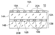
도 1 내지 도 3 에 나타내는 바와 같이, 본 실시형태에 따른 제 1 터치 패널용 도전 시트 (10) 는, 기재 (14A) 상에, 금속 세선으로 구성된 전극 패턴 (16A) (16B) 과 전극 패턴 (16A) (16B) 의 단부에 전기적으로 접속된 전극 단자 (60A) (60B) 를 갖는 도전 시트 (12A) (12B) 이고, 전극 패턴 (16A) (16B) 의 투과율이 83 % 이상이며, 전극 패턴 (16A) (16B) 의 투과율을 a % 로 나타낼 때에, 전극 단자 (60A) (60B) 의 투과율이 (a-20) % 이상 (a-3) % 이하이다. 또한, 다른 양태로서, 본 실시형태에 따른 제 1 터치 패널용 도전 시트 (10) 는, 기재 (14A) 상에, 금속 세선으로 구성된 전극 패턴 (16A) (16B) 과 전극 패턴 (16A) (16B) 의 단부에 전기적으로 접속된 전극 단자 (60A) (60B) 를 갖는 도전 시트 (12A) (12B) 이고, 전극 패턴 (16A) (16B) 의 개구율이 90 % 이상이며, 전극 패턴 (16A) (16B) 의 개구율을 b % 로 나타냈을 때, 전극 단자 (60A) (60B) 의 개구율이 (b-20) % 이상 (b-0.1) % 이하이다.1 to 3, the
도 1 및 도 2 에 나타내는 바와 같이, 본 실시형태에 따른 제 2 터치 패널용 도전 시트 (10) 는, 금속 세선으로 구성된 전극 패턴 (16A) (16B) 과 전극 패턴 (16A) (16B) 의 단부에 전기적으로 접속된 전극 단자 (60A) (60B) 를 갖는 도전 시트 (12A) (12B) 이고, 전극 단자 (60A) (60B) 는, 금속 세선으로 구성된 프레임 형상 (64) 을 포함한다.1 and 2, the
도 1 및 도 2 에 나타내는 바와 같이, 본 실시형태에 따른 제3 터치 패널용 도전 시트 (10) 는, 금속 세선으로 구성된 전극 패턴 (16A) (16B) 과 전극 패턴 (16A) (16B) 의 단부에 전기적으로 접속된 전극 단자 (60A) (60B) 를 갖는 도전 시트 (12A) (12B) 이고, 전극 단자 (60A) (60B) 는 금속 세선으로 구성된 격자들 (68) 로 이루어진 메시 형상 (66) 을 포함한다.As shown in Figs. 1 and 2, the
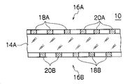
또한, 본 실시형태에 따른 터치 패널용 도전 시트 (10) 는, 도 4a 또는 도 4b 및 도 5a 에 나타내는 바와 같이, 제 1 도전 시트 (12A) 및 제 2 도전 시트 (12B) 를 적층 (라미네이트) 하여 구성된다.4A or 4B and 5A, the first
제 1 도전 시트 (12A) 는, 도 4a, 도 4b 및 도 6a 에 나타내는 바와 같이, 제 1 투명 기재 (14A) (도 5a 참조) 의 일 주면 상에 형성된 제 1 전극 패턴 (16A) 을 갖는다. 제 1 전극 패턴 (16A) 은, 금속 세선으로 이루어진 다수의 격자들로 구성된다. 제 1 전극 패턴 (16A) 은, 각각 제 1 방향 (x 방향) 으로 연장하고 제 1 방향에 직교하는 제 2 방향 (y 방향) 으로 배열된 2 이상의 제 1 도전 패턴들 (18A), 및 각각의 제 1 도전 패턴들 (18A) 을 전기적으로 분리하는 제 1 비도전 패턴들 (20A) 을 갖는다. 제 1 비도전 패턴 (20A) 에는, 금속 세선들의 교차부들 이외에 복수의 단선부들 (22A) 이 형성된다. 복수의 단선부들 (22A) 에 의해 각각의 제 1 도전 패턴들 (18A) 이 전기적으로 분리된다.The first
제 1 전극 패턴 (16A) 을 구성하는 금속 세선은 30 ㎛ 이하, 바람직하게는 15 ㎛ 이하, 더욱 바람직하게는 10 ㎛ 이하, 더욱 바람직하게는 9 ㎛ 이하, 더욱 바람직하게는 7 ㎛ 이하의 선폭을 갖는다. 선폭의 하한치는 1 ㎛ 가 바람직하다. 또한, 제 1 도전 패턴 (18A) 및 제 1 비도전 패턴 (20A) 은 실질적으로 동일한 선폭을 갖지만, 도 6a 에서는, 제 1 도전 패턴 (18A) 및 제 1 비도전 패턴 (20A) 을 명확하게 하기 위해, 제 1 도전 패턴 (18A) 의 선폭이 굵고 제 1 비도전 패턴 (20A) 의 선폭이 가늘게 되도록 패턴들이 과장되어 나타나 있다. 제 1 도전 패턴 (18A) 의 선폭 및 제 1 비도전 패턴 (20A) 의 선폭은 동일할 수도 있고 또는 상이할 수도 있다. 두 패턴들의 선폭들은 동일한 것이 바람직하다. 그 이유는, 선폭이 상이할 경우 시인성이 때때로 악화되기 때문이다. 제 1 전극 패턴 (16A) 의 금속 세선은 금, 은 및 구리와 같은 금속 재료, 및 금속 산화물의 도전 재료로 구성되고, 불투명한 도전 재료로 구성된다.The metal thin line constituting the
제 1 전극 패턴 (16A) 은, 교차하는 금속 세선들로 구성되는 복수의 격자들 (24A) 을 포함한다. 격자 (24A) 는 금속 세선으로 둘러싸이는 개구 영역을 포함한다. 격자들 (24A) 은 300 ㎛ 이상 800 ㎛ 이하, 바람직하게는 400 ㎛ 이상 600 ㎛ 이하의 격자 피치 Pa 를 갖는다. 제 1 도전 패턴 (18A) 의 격자들 (24A) 및 제 1 비도전 패턴 (20A) 의 격자들 (24A) 은 실질적으로 동일한 크기를 갖는다.The
제 1 비도전 패턴 (20A) 의 격자 (24A) 는 금속 세선들의 교차부들 이외에 단선부들 (22A) 을 갖는다. 제 1 비도전 패턴 (20A) 을 구성하는 모든 격자들 (24A) 이 단선부 (22A) 를 가질 필요는 없으며, 제 1 비도전 패턴 (20A) 이 인접하는 제 1 도전 패턴들 (18A) 간의 전기적인 분리를 달성할 수 있으면 된다. 단선부 (22A) 의 길이는 60 ㎛ 이하인 것이 바람직하다. 단선부 (22A) 의 길이의 하한치는 10 ㎛ 가 바람직하고, 15 ㎛ 가 보다 바람직하고, 20 ㎛ 가 더욱 바람직하다. 단선부 (22A) 의 길이의 상한치는 50 ㎛ 가 바람직하고, 40 ㎛ 가 보다 바람직하고, 30 ㎛ 가 더욱 바람직하다. 바람직한 범위는 10 ㎛ 이상 50 ㎛ 이하이며, 15 ㎛ 이상 30 ㎛ 이하이다. 또, 단선부 (22A) 를 형성하는 범위는, 예를 들어, 선밀도의 편차로 표현될 수 있다. 여기서, 선밀도의 편차는 단위 소격자 중의 총 세선 길이의 편차이며, ±(총 선 길이의 최대치 - 총 선 길이의 최소치)/총 선 길이 평균치/2 (%) 로 정의될 수 있다. 단선부 (22A) 를 형성하는 범위에서 선 밀도의 편차는 ± 15 % 이며, 보다 바람직하게는 ± 10 % 이다.The
상기 기재된 터치 패널용 도전 시트 (10) 에서, 격자 (24A) 는 대략 마름모꼴 형상을 갖는다. 여기서 대략 마름모꼴 형상이란, 대각 선들이 실질적으로 서로 직교하는 평행 사변형을 의미한다. 하지만, 그 형상은 또한, 대략 마름모꼴 형상 이외에, 다각형 형상일 수도 있다. 또, 일 변의 형상은 또한, 직선 형상 이외에, 만곡 형상 또는 원호 형상일 수도 있다. 그 형상이 원호 형상으로 형성되는 경우에, 예를 들어 2 개의 대향하는 변들은 바깥쪽으로 볼록하도록 한 원호 형상으로 형성될 수도 있고, 나머지 대향하는 변들은 안쪽으로 볼록하도록 한 원호 형상으로 형성될 수도 있다. 또한, 각각의 변의 형상은, 바깥쪽으로 볼록한 원호 형상 및 안쪽으로 볼록한 원호 형상이 연속하는 파선 형상일 수도 있다. 물론, 각각의 변의 형상은 사인 곡선일 수도 있다.In the
각각의 제 1 도전 패턴들 (18A) 은, 제 1 방향 (x 방향) 으로 교대로 배열된 대폭 부분 (wide portion) 및 협폭 부분 (narrow portion) 을 가지며, 이른바 다이아몬드 패턴을 형성한다. 유사하게, 각각의 제 1 비도전 패턴들 (20A) 은, 제 1 방향 (x 방향) 으로 교대로 배열된 대폭 부분 및 협폭 부분을 갖는다. 제 1 도전 패턴 (18A) 의 대폭 부분 및 협폭 부분의 순서는, 제 1 비도전 패턴 (20A) 의 대폭 부분 및 협폭 부분의 순서에 반대로 되어 있다. 또한, 각각의 제 1 도전 패턴들 (18A) 은 상기 기재된 다이아몬드 패턴에 한정되지 않고, 미리결정된 폭을 갖는 벨트 형상 (스트라이프 형상), 미리결정된 폭을 갖는 지그재그 형상 등일 수도 있다. 패터닝은, 기존의 ITO 투명 도전막에서 형성되는 전극 형상을 포함한다.Each of the first
각각의 제 1 도전 패턴들 (18A) 의 일 단부는 제 1 전극 단자 (60A) 를 개재하여 제 1 외부 배선 (62A) 에 전기적으로 접속된다. 한편, 각각의 제 1 도전 패턴 (18A) 의 다른 단부는 개방 단부이다. 또한, 각각의 제 1 도전 패턴 (18A) 의 다른 단부는, 외부 배선에 전기적으로 접속되지 않는 것 이외에는 일 단부와 유사한 패턴 형상 및 단자를 갖는 형상으로 형성될 수도 있다.One end of each first
제 2 도전 시트 (12B) 는, 도 4a, 도 4b 및 도 6b 에 나타내는 바와 같이, 제 2 투명 기재 (14B) (도 5a 참조) 의 일 주면 상에 형성된 제 1 전극 패턴 (16B) 을 갖는다. 제 2 전극 패턴 (16B) 은, 금속 세선으로 이루어진 다수의 격자들로 구성된다. 제 2 전극 패턴 (16B) 은, 각각 제 2 방향 (y 방향) 으로 연장하고 제 2 방향에 직교하는 제 1 방향 (x 방향) 으로 배열된 2 이상의 제 2 도전 패턴들 (18B), 및 각각의 제 2 도전 패턴들 (18B) 을 전기적으로 분리하는 제 2 비도전 패턴들 (20B) 을 갖는다. 제 2 비도전 패턴 (20B) 에는, 금속 세선들의 교차부들 이외에 복수의 단선부들 (22B) 이 형성된다. 복수의 단선부들 (22B) 에 의해 각각의 제 2 도전 패턴들 (18B) 이 전기적으로 분리된다.The second
제 2 전극 패턴 (16B) 을 구성하는 금속 세선은 제 1 전극 패턴 (16A) 을 구성하는 금속 세선의 선폭과 실질적으로 동일한 선폭을 갖는다. 또한, 제 2 도전 패턴 (18B) 및 제 2 비도전 패턴 (20B) 은 실질적으로 동일한 선폭을 갖지만, 도 6b 에서는, 제 2 도전 패턴 (18B) 및 제 2 비도전 패턴 (20B) 을 명확하게 하기 위해, 제 2 도전 패턴 (18B) 의 선폭이 굵고 제 2 비도전 패턴 (20B) 의 선폭이 가늘게 되도록 패턴들이 과장되어 나타나 있다. 제 2 도전 패턴 (18B) 의 선폭 및 제 2 비도전 패턴 (20B) 의 선폭은 동일할 수도 있고 또는 상이할 수도 있다. 두 패턴들의 선폭들은 동일한 것이 바람직하다. 그 이유는, 선폭이 상이할 경우 시인성이 때때로 악화되기 때문이다.The metal thin line constituting the
제 2 전극 패턴 (16B) 의 금속 세선은 제 1 전극 패턴 (16A) 의 금속 세선의 도전 재료와 동일한 도전 재료로 구성된다.The metal thin line of the
제 2 전극 패턴 (16B) 은, 교차하는 금속 세선들로 구성되는 복수의 격자들 (24B) 을 포함한다. 격자 (24B) 는 금속 세선으로 둘러싸이는 개구 영역을 포함한다. 격자들 (24B) 은 300 ㎛ 이상 800 ㎛ 이하, 바람직하게는 400 ㎛ 이상 600 ㎛ 이하의 격자 피치 Pb 를 갖는다. 제 2 도전 패턴 (18B) 의 격자들 (24B) 및 제 2 비도전 패턴 (20B) 의 격자들 (24B) 은 실질적으로 동일한 크기를 갖는다.The
제 2 비도전 패턴 (20B) 의 격자 (24B) 는 금속 세선들의 교차부들 이외에 단선부들 (22B) 을 갖는다. 제 2 비도전 패턴 (20B) 을 구성하는 모든 격자들 (24B) 이 단선부 (22B) 를 가질 필요는 없으며, 제 2 비도전 패턴 (20B) 이 인접하는 제 2 도전 패턴들 (18B) 간의 전기적인 분리를 달성할 수 있으면 된다. 단선부 (22B) 의 길이는 60 ㎛ 이하인 것이 바람직하다. 단선부 (22B) 의 길이의 하한치는 10 ㎛ 가 바람직하고, 15 ㎛ 가 보다 바람직하고, 20 ㎛ 가 더욱 바람직하다. 단선부 (22B) 의 길이의 상한치는 50 ㎛ 가 바람직하고, 40 ㎛ 가 보다 바람직하고, 30 ㎛ 가 더욱 바람직하다. 바람직한 범위는 10 ㎛ 이상 50 ㎛ 이하이며, 15 ㎛ 이상 30 ㎛ 이하이다. 또, 단선부 (22B) 를 형성하는 범위는, 예를 들어, 선밀도의 편차로 표현될 수 있다. 여기서, 선밀도의 편차는 단위 소격자 중의 총 세선 길이의 편차이며, ±(총 선 길이의 최대치 - 총 선 길이의 최소치)/총 선 길이 평균치/2 (%) 로 정의될 수 있다. 단선부 (22B) 를 형성하는 범위에서 선 밀도의 편차는 ± 15 % 이며, 보다 바람직하게는 ± 10 % 이다.The
상기 기재된 터치 패널용 도전 시트 (10) 에서, 격자 (24B) 는 대략 마름모꼴 형상을 갖는다. 여기서 대략 마름모꼴 형상이란, 대각 선들이 실질적으로 서로 직교하는 평행 사변형을 의미한다. 하지만, 그 형상은 또한, 대략 마름모꼴 형상 이외에, 다각형 형상일 수도 있다. 또, 일 변의 형상은 또한, 직선 형상 이외에, 만곡 형상 또는 원호 형상일 수도 있다. 그 형상이 원호 형상으로 형성되는 경우에, 예를 들어 2 개의 대향하는 변들은 바깥쪽으로 볼록하도록 한 원호 형상으로 형성될 수도 있고, 나머지 대향하는 변들은 안쪽으로 볼록하도록 한 원호 형상으로 형성될 수도 있다. 또한, 각각의 변의 형상은, 바깥쪽으로 볼록한 원호 형상 및 안쪽으로 볼록한 원호 형상이 연속하는 파선 형상일 수도 있다. 물론, 각각의 변의 형상은 사인 곡선일 수도 있다.In the
각각의 제 2 도전 패턴들 (18B) 은, 제 2 방향 (y 방향) 으로 교대로 배열된 대폭 부분 및 협폭 부분을 가지며, 이른바 다이아몬드 패턴을 형성한다. 유사하게, 각각의 제 2 비도전 패턴들 (20B) 은, 제 2 방향 (y 방향) 으로 교대로 배열된 대폭 부분 및 협폭 부분을 갖는다. 제 2 도전 패턴 (18B) 의 대폭 부분 및 협폭 부분의 순서는, 제 2 비도전 패턴 (20B) 의 대폭 부분 및 협폭 부분의 순서에 반대로 되어 있다.Each of the second
각각의 제 2 도전 패턴들 (18B) 의 일 단부는 제 2 전극 단자 (60B) 를 개재하여 제 2 외부 배선 (62B) 에 전기적으로 접속된다. 한편, 각각의 제 2 도전 패턴 (18B) 의 다른 단부는 개방 단부이다.One end of each second
또한, 예를 들어 제 2 도전 시트 (12B) 상에 제 1 도전 시트 (12A) 를 적층하여 터치 패널용 도전 시트 (10) 를 형성할 때에, 도 7 에 나타내는 바와 같이, 제 1 전극 패턴 (16A) 은 제 2 전극 패턴 (16B) 과 중첩하지 않도록 배열된다. 이때, 제 1 도전 패턴 (18A) 의 협폭 부분이 제 2 도전 패턴 (18B) 의 협폭 부분에 대향하고 그리고 제 1 도전 패턴 (18A) 의 협폭 부분이 제 2 도전 패턴 (18B) 의 협폭 부분과 교차하도록 제 1 전극 패턴 (16A) 및 제 2 전극 패턴 (16B) 이 배열된다. 이 결과, 제 1 전극 패턴 (16A) 및 제 2 전극 패턴 (16B) 에 의해 조합 패턴 (70) 이 형성된다. 또한, 제 1 전극 패턴 (16A) 및 제 2 전극 패턴 (16B) 의 각각의 선폭은 실질적으로 서로 동일하다. 또, 격자들 (24A) 및 격자들 (24B) 의 각각의 크기는 실질적으로 서로 동일하다. 하지만, 도 6a 및 도 6b 에서는, 제 1 전극 패턴 (16A) 과 제 2 전극 패턴 (16B) 간의 위치 관계를 명확하게 하기 위해, 제 1 전극 패턴 (16A) 의 선폭을 제 2 전극 패턴 (16B) 의 선폭보다 더 굵게 나타내고 있다.7, when the
조합 패턴 (70) 에 있어서, 상면에서 보았을 때에, 격자들 (24A) 및 격자들 (24B) 에 의해 소격자들이 형성된다. 구체적으로, 격자들 (24A) 의 교차부들이 격자들 (24B) 의 개구 영역들에 배열된다. 또한, 소격자들은 격자들 (24A) 및 격자들 (24B) 의 격자 피치 Pa 및 Pb 의 절반인 150 ㎛ 이상 400 ㎛ 이하, 바람직하게는 200 ㎛ 이상 300 ㎛ 이하의 격자 피치 Ps 를 갖는다.In the
제 1 비도전 패턴 (20A) 의 단선부들 (22A) 은 격자들 (24A) 의 교차부들 이외에 형성되고, 제 2 비도전 패턴 (20B) 의 단선부들 (22B) 은 격자들 (24B) 의 교차부들 이외에 형성된다. 그 결과, 조합 패턴 (70) 에 있어서, 단선부 (22A) 및 단선부 (22B) 에서 기인되는 시인성의 열화를 방지할 수 있다.The
특히 단선부들 (22A) 에 대향하는 위치에, 제 2 도전 패턴 (18B) 의 금속 세선이 배열된다. 또한, 단선부들 (22B) 에 대향하는 위치에, 제 1 도전 패턴 (18A) 의 금속 세선이 배열된다. 제 2 도전 패턴 (18B) 의 금속 세선이 단선부들 (22A) 을 마스킹하고, 제 1 도전 패턴 (18A) 의 금속 세선이 단선부들 (22B) 을 마스킹한다. 따라서, 조합 패턴 (70) 에 있어서, 상면에서 보았을 때에, 단선부들 (22A) 및 단선부들 (22B) 이 인지되기 어려워지므로, 시인성이 향상될 수 있다. 시인성 향상을 고려하면, 단선부들 (22A) 의 길이 및 제 2 도전 패턴 (18B) 의 금속 세선의 선폭은, 선폭 × 1 < 단선부 < 선폭 × 10 의 관계식을 만족하는 것이 바람직하다. 유사하게, 단선부들 (22B) 의 길이 및 제 1 도전 패턴 (18A) 의 금속 세선의 선폭은, 선폭 × 1 < 단선부 < 선폭 × 10 의 관계식을 만족하는 것이 바람직하다.In particular, metal thin wires of the second
이 터치 패널용 도전 시트 (10) 를 터치 패널로서 사용할 때에, 제 1 도전 시트 (12A) 상에 보호층 (도시 생략) 이 형성된다. 제 1 도전 시트 (12A) 의 다수의 각각의 제 1 도전 패턴들 (18A) 로부터 도출된 제 1 외부 배선들 (62A), 및 제 2 도전 시트 (12B) 의 다수의 각각의 제 2 도전 패턴들 (18B) 로부터 도출된 제 2 외부 배선 (62B) 은, 예를 들어 스캐닝을 제어하는 IC 회로에 접속된다.When the
터치 패널용 도전 시트 (10) 중에서, 액정 표시 장치의 표시 화면 밖의 외주 영역에서의 면적을 최소화하기 위해, 제 1 도전 패턴 (18A) 과 제 1 외부 배선 (62A) 간의 각각의 접속부가 선형으로 배열되고 그리고 제 2 도전 패턴 (18B) 과 제 2 외부 배선 (62B) 간의 각각의 접속부가 선형으로 배열되는 것이 바람직하다.The respective connecting portions between the first
손가락을 보호층과 접촉시킬 때에, 손가락에 대향하는 제 1 도전 패턴 (18A) 과 제 2 도전 패턴 (18B) 간의 정전용량이 변화한다. IC 회로는 이 변화량을 검출하여, 이 변화량에 기초하여 손가락의 위치를 연산한다. 이 연산은 각각의 제 1 도전 패턴 (18A) 과 제 2 도전 패턴 (18B) 사이에서 수행된다. 따라서, 동시에 2 개 이상의 손가락들을 보호층과 접촉시키더라도, 각각의 손가락들의 위치들을 검출할 수 있다.The capacitance between the first
이와 같이, 터치 패널용 도전 시트 (10) 가, 예를 들어 투영형 정전용량방식의 터치 패널에 적용되어 사용될 경우에, 터치 패널용 도전 시트 (10) 에서의 표면 저항이 작기 때문에 응답 속도를 증가시킬 수 있고, 터치 패널의 크기를 증대시키는 동향을 촉진시킬 수 있다.As described above, when the
그러나, 종래의 금속 세선을 전극들에 사용한 터치 패널에서는, 높은 도전성을 제공하기 위해 굵은 단자들 (솔리드 단자들) 이 전극 단자들 (60A 및 60B) 로서 사용되어 있다. 따라서, 디스플레이 및 터치 패널을 조합하여 작동시키는 경우, 터치 패널의 센싱 영역 (전극 패턴) 에서 디스플레이로부터 방출되는 광을 전극 단자들이 차광한다. 그리하여, 센싱 영역에서의 전극 단자들 근방에서 어두워진 부분이 나타나고, 그 부분에서의 디스플레이가 잘 보이지 않게 된다.However, in the touch panel using the conventional metal thin wire as the electrodes, thick terminals (solid terminals) are used as the
그리하여, 본 발명은 이하에 기재되는 제 1 내지 제 3 터치 패널용 도전 시트들을 달성하였다.Thus, the present invention achieves the first to third conductive sheets for a touch panel described below.
(제 1 터치 패널용 도전 시트)(Conductive sheet for the first touch panel)
본 발명에 따른 제 1 터치 패널용 도전 시트는, 기재 (14A) 상에, 금속 세선으로 구성된 전극 패턴 (16A) (16B) 및 전극 패턴 (16A) (16B) 의 단부에 전기적으로 접속된 전극 단자 (60A) (60B) 를 갖는 상기 기재된 도전 시트 (12A) (12B) 이고, 전극 패턴 (16A) (16B) 은 투과율이 83 % 이상이도록 구성되며, 전극 패턴 (16A) (16B) 의 투과율을 a % 로 나타낼 때에, 전극 단자 (60A) (60B) 의 투과율이 (a-20) % 이상 (a-3) % 이하이도록 구성된다. 또한, 전극 단자 (60A) (60B) 의 투과율은, 보다 바람직하게는 (a-15) % 이상 (a-3) % 이하이며, 더욱 바람직하게는 (a-10) 이상 (a-3) 이하이며, 가장 바람직하게는 (a-5) 이상 (a-3) 이하의 범위이다.The conductive sheet for a first touch panel according to the present invention includes
또한, 본 발명에 따른 다른 양태의 제 1 터치 패널용 도전 시트는, 기재 (14A) 상에, 금속 세선으로 구성된 전극 패턴 (16A) (16B) 및 전극 패턴 (16A) (16B) 의 단부에 전기적으로 접속된 전극 단자 (60A) (60B) 를 갖는 상기 기재된 도전 시트 (12A) (12B) 이고, 전극 패턴 (16A) (16B) 은 개구율이 90 % 이상이도록 구성되며, 전극 패턴 (16A) (16B) 의 개구율을 b % 로 나타낼 때에, 전극 단자 (60A) (60B) 의 개구율이 (b-20) % 이상 (b-0.1) % 이하이도록 구성된다. 또한, 개구율은, 보다 바람직하게는 (b-10) 이상 (b-0.3) 이하이며, 더욱 바람직하게는 (b-5) 이상 (b-0.3) 이하의 범위이다.The conductive sheet for the first touch panel according to another embodiment of the present invention is characterized in that the
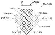
도 1 은 전극 단자 (60A) (60B) 가 금속 세선으로 구성된 프레임 형상 (64) 을 갖는 예를 나타낸다. 여기서, 전극 패턴 (16A) (16B) 의 세선의 선폭을 A (㎛) 로 나타낼 때에, 전극 단자 (60A) (60B) 의 프레임 형상의 선폭 B (㎛) 는 B≥2A 또는 B≥A+5 (㎛) 를 만족하는 것이 바람직하다. 상기 기재된 전극 패턴의 세선의 선폭 a (㎛) 는 30 ㎛ 이하가 바람직하다.1 shows an example in which the
도 1 에 나타내는 바와 같이, 전극 단자 (60A) (60B) 는 금속 세선으로 구성된 프레임 형상 (64) 을 갖도록 구조화되므로, 전극 패턴 (16A) (16B) 의 투과율이 83 % 이상이 될 수 있고, 전극 패턴 (16A) (16B) 의 투과율을 a % 로 나타낼 때에, 전극 단자 (60A) (60B) 의 투과율이 (a-20) % 이상 (a-3) % 이하로 될 수 있다.The
또, 전극 단자 (60A) (60B) 는 금속 세선으로 구성된 프레임 형상 (64) 을 갖도록 구조화되므로, 전극 패턴 (16A) (16B) 의 개구율이 90 % 이상이 될 수 있고, 전극 패턴 (16A) (16B) 의 개구율을 b % 로 나타낼 때에, 전극 단자 (60A) (60B) 의 개구율이 (b-20) % 이상 (b-0.1) % 이하로 될 수 있다.Since the
따라서, 전극 단자 (60A) (60B) 가 금속 세선으로 구성된 프레임 형상 (64) 이도록 구조화될 때에, 종래의 굵은 단자 (솔리드 단자) 와는 달리, 터치 패널의 센싱 영역 (전극 패턴) 에서 디스플레이로부터 방출되는 광을 전극 단자가 차광하기 어려워진다. 그리하여, 센싱 영역의 전극 단자 근방에서 어두워진 부분이 나타나지 않는다. 따라서, 센싱 영역의 전극 단자 근방에서 시인성이 손상되지 않는다.Therefore, when the
도 2 는 전극 단자 (60A) (60B) 가 금속 세선으로 구성된 격자들 (68) 로 이루어진 메시 형상 (66) 을 갖는 예를 나타낸다. 여기서, 전극 단자 (60A) (60B) 의 메시 형상 (66) 의 피치는, 전극 패턴 (16A) (16B) 의 피치보다 더 조밀한 것이 바람직하고, 전극 패턴 (16A) (16B) 의 피치의 3/4 이하가 보다 바람직하고, 전극 패턴 (16A) (16B) 의 피치의 2/3 이하가 더욱 바람직하고, 전극 패턴 (16A) (16B) 의 피치의 1/2 이 더욱 더 바람직하다. 전극 단자의 메시 형상의 피치가 전극 패턴의 피치보다 더 작게 될 때에, 전극 단자의 전기 특성들을 향상시킬 수 있고, 신호 검출의 안정성을 유지할 수 있다. 전극 단자 (60A) (60B) 의 메시 형상 (66) 의 피치는, 50 ㎛ 이상 300 ㎛ 이하이며, 50 ㎛ 이상 250 ㎛ 이하가 보다 바람직하다. 또한, 전극 패턴 (16A) (16B) 의 피치는, 격자 (24A) (24B) 의 한 변의 길이와 대략 동등한 값이다.Fig. 2 shows an example in which the
도 2 에 나타내는 바와 같이, 전극 단자 (60A) (60B) 는 금속 세선으로 구성된 격자들 (68) 로 이루어진 메시 형상 (66) 을 갖도록 구조화되므로, 전극 패턴 (16A) (16B) 의 투과율이 83 % 이상으로 될 수 있고, 전극 패턴 (16A) (16B) 의 투과율을 a % 로 나타낼 때에, 전극 단자 (60A) (60B) 의 투과율이 (a-20) % 이상 (a-3) % 이하로 될 수 있다.The
또, 전극 단자 (60A) (60B) 가 금속 세선으로 구성된 격자들 (68) 로 이루어진 메시 형상 (66) 을 가지도록 구조화될 때에, 전극 패턴 (16A) (16B) 의 개구율은 90 % 이상으로 될 수 있고, 전극 패턴 (16A) (16B) 의 개구율을 b % 로 나타낼 때에, 전극 단자 (60A) (60B) 의 개구율이 (b-20) % 이상 (b-0.1) % 이하로 될 수 있다.When the
따라서, 전극 단자 (60A) (60B) 가 금속 세선으로 구성된 메시 형상 (66) 을 갖도록 구조화될 때에, 종래의 굵은 단자 (솔리드 단자) 와는 달리, 터치 패널의 센싱 영역 (전극 패턴) 에서 디스플레이로부터 방출되는 광을 전극 단자가 차광하기 어려워지므로, 센싱 영역의 전극 단자 근방에서 어두워진 부분이 나타나지 않는다. 따라서, 센싱 영역의 전극 단자 근방에서 시인성은 손상되지 않는다.Therefore, when the
도 3 은 전극 단자 (60A) (60B) 가 금속 세선으로 구성된 프레임 형상 (64); 및 금속 세선으로 구성된 격자들 (68) 로 이루어진 메시 형상 (66) 으로 이루어지는 예를 나타낸다.Fig. 3 shows a case where the
도 3 에 나타내는 바와 같이, 전극 단자 (60A) (60B) 는, 금속 세선으로 구성된 프레임 형상 (64); 및 금속 세선으로 구성된 격자들 (68) 로 이루어진 메시 형상 (66) 으로 이루어지며, 이에 따라 전극 패턴 (16A) (16B) 의 투과율이 83 % 이상으로 될 수 있고, 전극 패턴 (16A) (16B) 의 투과율을 a % 로 나타낼 때에, 전극 단자 (60A) (60B) 의 투과율이 (a-20) % 이상 (a-3) % 이하로 될 수 있다.As shown in Fig. 3, the
또, 전극 단자 (60A) (60B) 가 금속 세선으로 구성된 프레임 형상 (64); 및 금속 세선으로 구성된 격자들 (68) 로 이루어진 메시 형상 (66) 으로 이루어질 때에, 전극 패턴 (16A) (16B) 의 개구율이 90 % 이상으로 될 수 있고, 전극 패턴 (16A) (16B) 의 개구율을 b % 로 나타낼 때에, 전극 단자 (60A) (60B) 의 개구율이 (b-20) % 이상 (b-0.1) % 이하로 될 수 있다.Further, the
따라서, 전극 단자 (60A) (60B) 가 금속 세선으로 구성된 프레임 형상 (64); 및 금속 세선으로 구성된 격자들 (68) 로 이루어진 메시 형상 (66) 로 이루어질 때에, 종래의 굵은 단자 (솔리드 단자) 와는 달리, 터치 패널의 센싱 영역 (전극 패턴) 에서 디스플레이로부터 방출되는 광을 전극 단자가 차광하기 어려워지고, 따라서, 센싱 영역의 전극 단자 근방에서 어두워진 부분이 나타나지 않는다. 따라서, 센싱 영역의 전극 단자 근방에서 시인성은 손상되지 않는다.Accordingly, the
또한, 도 2 및 도 3 의 메시 형상 (66) 에서, 격자 (68) 는 대략 마름모꼴 형상을 갖는다. 여기서 대략 마름모꼴 형상이란, 대각 선들이 실질적으로 서로 직교하는 평행 사변형을 의미한다. 하지만, 그 형상은 또한, 대략 마름모꼴 형상 이외에, 다각형 형상일 수도 있다. 또, 일 변의 형상은 또한, 직선 형상 이외에, 만곡 형상 또는 원호 형상일 수도 있다. 그 형상이 원호 형상으로 형성되는 경우에, 예를 들어 2 개의 대향하는 변들은 바깥쪽으로 볼록하도록 한 원호 형상으로 형성될 수도 있고, 나머지 대향하는 변들은 안쪽으로 볼록하도록 한 원호 형상으로 형성될 수도 있다. 또한, 각각의 변의 형상은, 바깥쪽으로 볼록한 원호 형상 및 안쪽으로 볼록한 원호 형상이 연속하는 파선 형상일 수도 있다. 물론, 각각의 변의 형상은 사인 곡선일 수도 있다.2 and 3, the grating 68 has a substantially rhombic shape. Here, the substantially rhombic shape means a parallelogram shape in which diagonal lines are substantially orthogonal to each other. However, the shape may also be a polygonal shape other than a rough diamond shape. The shape of one side may be curved or circular in addition to a linear shape. In the case where the shape is formed into an arc shape, for example, the two opposing sides may be formed into an arc shape convex outwardly, and the remaining opposite sides may be formed into an arc shape convex inward . Further, the shape of each side may be a broken line shape in which an outwardly convex circular arc shape and an inwardly convex circular arc shape continue. Of course, the shape of each side may be a sinusoidal curve.
본 발명에 따른 전극 단자 (60A) (60B) 에 있어서, 전극 패턴에 전기적으로 접속된 부분과 외부 배선 (62A) (62B) 간의 저항은 1 내지 100 Ω 의 범위인 것이 바람직하다. 또, 도 2 및 도 3 에 나타내는 바와 같이 전극 단자 (60A) (60B) 가 메시 형상 (66) 을 포함하는 경우에, 전극 단자 (60A) (60B) 의 표면 저항값은 4 Ω/sq. 이상 80 Ω/sq. 이하의 범위인 것이 바람직하고, 10 Ω/sq. 이상 40 Ω/sq. 이하의 범위인 것이 더욱 바람직하다.In the
또한, 개구율은, 전극 단자 (60A) (60B) 에서 금속 세선을 제외한 투광성 부분이 전체에 차지하는 비율이다. 예를 들어, 선폭 15 ㎛ 및 피치 300 ㎛ 인 정방형의 격자 (68) 의 개구율은 90 % 이다.The aperture ratio is the ratio of the light-transmitting portions excluding the metal thin wires in the
(제 2 터치 패널용 도전 시트)(Conductive sheet for second touch panel)
본 발명에 따른 제 2 터치 패널용 도전 시트는, 기재 (14A) 상에, 금속 세선으로 구성된 전극 패턴 (16A) (16B) 및 전극 패턴 (16A) (16B) 의 단부에 전기적으로 접속된 전극 단자 (60A) (60B) 를 갖는 상기 기재된 도전 시트 (12A) (12B) 이고, 전극 단자 (60A) (60B) 는 금속 세선으로 구성된 프레임 형상 (64) 를 포함하도록 구성된다.The conductive sheet for a second touch panel according to the present invention includes
도 1 은 전극 단자 (60A) (60B) 가 금속 세선으로 구성된 프레임 형상 (64) 인 예를 나타낸다.1 shows an example in which the
여기서, 전극 패턴 (16A) (16B) 의 세선의 선폭을 A (㎛) 로 나타낼 때에, 전극 단자 (60A) (60B) 의 프레임 형상의 선폭 B (㎛) 는 B ≥ 2A 또는 B ≥ A+5 (㎛) 를 만족하는 것이 바람직하다. 프레임 형상의 선폭 B (㎛) 는, 보다 바람직하게 50 ㎛ ≥ B ≥ 10 ㎛ 의 범위이며, 더욱 바람직하게는 30 ㎛ ≥ B ≥ 15 ㎛의 범위이다. 또 프레임 형상 (64) 은 대략 직사각형 형상이고, 그 가로폭은 전극 패턴의 최대 가로폭과 대략 같은 길이이지만, 전극 패턴의 최대 가로폭보다 더 작을 수도 있다. 또한, 가로폭이 전극 패턴의 최대 가로폭보다 극히 더 작으면, 전기 저항이 커진다. 따라서, 가로폭은 전극 패턴의 최대 가로폭의 1/3이상이 바람직하고, 전극 패턴의 최대 가로폭의 1/2 이상이 보다 바람직하다.Here, when the line width of the fine lines of the
도 1 에 나타내는 바와 같이, 전극 단자 (60A) (60B) 는 금속 세선으로 구성된 프레임 형상 (64) 이도록 구조화되고, 이에 따라 종래의 굵은 단자 (솔리드 단자) 와는 달리, 터치 패널의 센싱 영역 (전극 패턴) 에서 디스플레이로부터 방출되는 광을 전극 단자가 차광하기 어려워지고, 따라서 센싱 영역의 전극 단자 근방에서 어두워진 부분이 나타나지 않는다. 따라서, 센싱 영역의 전극 단자 근방에서 시인성은 손상되지 않는다. 또, 이와 같은 형상을 채용하는 경우에, 전기 신호의 노이즈를 증가시키지 않고 구성성분들의 사용량을 저감할 수 있고, 도전막의 제조 비용을 저감할 수 있다는 효과가 또한 있다.As shown in Fig. 1, the
도 3 은 전극 단자 (60A) (60B) 가 금속 세선으로 구성된 프레임 형상 (64); 및 금속 세선으로 구성된 격자들 (68) 로 이루어진 메시 형상 (66) 으로 이루어지는 예를 나타낸다. 여기서, 전극 단자 (60A) (60B) 의 메시 형상 (66) 의 피치는, 전극 패턴 (16A) (16B) 의 피치보다 더 조밀한 것이 바람직하고, 전극 패턴 (16A) (16B) 의 피치의 3/4 이하가 보다 바람직하고, 전극 패턴 (16A) (16B) 의 피치의 2/3 이하가 더욱 바람직하고, 전극 패턴 (16A) (16B) 의 피치의 1/2 이 더욱 더 바람직하다. 전극 단자의 메시 형상의 피치가 전극 패턴의 피치보다 더 작게 될 때에, 전극 단자의 전기 특성들을 향상시킬 수 있고, 신호 검출의 안정성을 유지할 수 있다. 전극 단자 (60A) (60B) 의 메시 형상 (66) 의 피치는, 50 ㎛ 이상 300 ㎛ 이하이며, 50 ㎛ 이상 250 ㎛ 이하가 보다 바람직하다. 또한, 전극 패턴 (16A) (16B) 의 피치는, 격자 (24A) (24B) 의 한 변의 길이와 대략 동등한 값이다.Fig. 3 shows a case where the
도 3 에 나타내는 바와 같이, 전극 단자 (60A) (60B) 는 금속 세선으로 구성된 프레임 형상 (64); 및 금속 세선으로 구성된 격자들 (68) 로 이루어진 메시 형상 (66) 으로 이루어지고, 이에 따라 종래의 굵은 단자 (솔리드 단자) 와는 달리, 터치 패널의 센싱 영역 (전극 패턴) 에서 디스플레이로부터 방출되는 광을 전극 단자가 차광하기 어려워지고, 따라서 센싱 영역의 전극 단자 근방에서 어두워진 부분이 나타나지 않는다. 따라서, 센싱 영역의 전극 단자 근방에서 시인성은 손상되지 않는다.As shown in Fig. 3, the
또한, 도 3 의 메시 형상 (66) 에서, 격자 (68) 는 대략 마름모꼴 형상을 갖는다. 여기서 대략 마름모꼴 형상이란, 대각 선들이 실질적으로 서로 직교하는 평행 사변형을 의미한다. 하지만, 그 형상은 또한, 대략 마름모꼴 형상 이외에, 다각형 형상일 수도 있다. 또, 일 변의 형상은 또한, 직선 형상 이외에, 만곡 형상 또는 원호 형상일 수도 있다. 그 형상이 원호 형상으로 형성되는 경우에, 예를 들어 2 개의 대향하는 변들은 바깥쪽으로 볼록하도록 한 원호 형상으로 형성될 수도 있고, 나머지 대향하는 변들은 안쪽으로 볼록하도록 한 원호 형상으로 형성될 수도 있다. 또한, 각각의 변의 형상은, 바깥쪽으로 볼록한 원호 형상 및 안쪽으로 볼록한 원호 형상이 연속하는 파선 형상일 수도 있다. 물론, 각각의 변의 형상은 사인 곡선일 수도 있다.Further, in the
본 발명에 따른 전극 단자 (60A) (60B) 에 있어서, 전극 패턴에 전기적으로 접속된 부분과 외부 배선 (62A) (62B) 간의 저항은 1 내지 100 Ω 의 범위인 것이 바람직하다. 또, 도 3 에 나타내는 바와 같이 전극 단자 (60A) (60B) 가 메시 형상 (66) 을 포함하는 경우에, 전극 단자 (60A) (60B) 의 표면 저항값은 4 Ω/sq. 이상 80 Ω/sq. 이하의 범위인 것이 바람직하고, 10 Ω/sq. 이상 40 Ω/sq. 이하의 범위인 것이 더욱 바람직하다.In the
또한, 개구율은, 전극 단자 (60A) (60B) 에서 금속 세선을 제외한 투광성 부분이 전체에 차지하는 비율이며, 예를 들어, 선폭 15 ㎛ 및 피치 300 ㎛ 인 정방형의 격자 (68) 의 개구율은 90 % 이다.The aperture ratio is the ratio of the light-transmitting portions excluding the metal thin wires in the
또, 본 발명에 있어서, 도 3 의 경우, 전극 패턴 (16A) (16B) 의 투과율이 83 % 이상이며, 전극 패턴 (16A) (16B) 의 투과율을 a % 로 나타낼 때에, 전극 단자 (60A) (60B) 의 투과율이 (a-20) % 이상 (a-3) % 이하인 것이 바람직하다.3, when the transmittance of the
게다가, 본 발명에 있어서, 도 3 의 경우, 전극 패턴 (16A) (16B) 의 개구율이 90 % 이상이며, 전극 패턴 (16A) (16B) 의 개구율을 b % 로 나타낼 때에, 전극 단자 (60A) (60B) 의 개구율이 (b-20) % 이상 (b-0.1) % 이하인 것이 바람직하다. 또한, 여기서 개구율이란, 전극 단자 (60A) (60B) 에서 금속 세선을 제외한 투광성 부분이 전체에 차지하는 비율이며, 예를 들어, 선폭 15 ㎛ 및 피치 300 ㎛ 인 정방형의 격자 (68) 의 개구율은 90 % 이다.3, when the aperture ratio of the
(제3 터치 패널용 도전 시트)(The conductive sheet for the third touch panel)
본 발명에 따른 제3 터치 패널용 도전 시트는, 기재 (14A) 상에, 금속 세선으로 구성된 전극 패턴 (16A) (16B); 및 전극 패턴 (16A) (16B) 의 단부에 전기적으로 접속된 전극 단자 (60A) (60B) 를 갖는 상기 기재된 도전 시트 (12A) (12B) 이고, 전극 단자 (60A) (60B) 는 금속 세선으로 구성된 격자들 (68) 로 이루어진 메시 형상 (66) 을 포함하도록 구성된다.The conductive sheet for a third touch panel according to the present invention comprises electrode patterns (16A) and (16B) composed of thin metal wires on a base material (14A); And the
도 2 는 전극 단자 (60A) (60B) 가 금속 세선으로 구성된 격자들 (68) 로 이루어진 메시 형상 (66) 을 갖는 예를 나타낸다.Fig. 2 shows an example in which the
여기서, 전극 단자 (60A) (60B) 의 메시 형상 (66) 의 피치는, 전극 패턴 (16A) (16B) 의 피치보다 더 조밀한 것이 바람직하고, 전극 패턴 (16A) (16B) 의 피치의 3/4 이하가 보다 바람직하고, 전극 패턴 (16A) (16B) 의 피치의 2/3 이하가 더욱 바람직하고, 전극 패턴 (16A) (16B) 의 피치의 1/2 이 더욱 더 바람직하다. 전극 단자의 메시 형상의 피치가 전극 패턴의 피치보다 더 작게 될 때에, 전극 단자의 전기 특성들을 향상시킬 수 있고, 신호 검출의 안정성을 유지할 수 있다. 전극 단자 (60A) (60B) 의 메시 형상 (66) 의 특정 피치는, 50 ㎛ 이상 300 ㎛ 이하이며, 50 ㎛ 이상 250 ㎛ 이하가 보다 바람직하다. 또한, 전극 패턴 (16A) (16B) 의 피치는, 격자 (24A) (24B) 의 한 변의 길이와 대략 동등한 값이다.It is preferable that the pitch of the mesh shapes 66 of the
도 3 에 나타내는 바와 같이, 전극 단자 (60A) (60B) 는 금속 세선으로 구성된 격자들 (68) 로 이루어진 메시 형상 (66) 을 갖도록 구조화되고, 이에 따라 종래의 굵은 단자 (솔리드 단자) 와는 달리, 터치 패널의 센싱 영역 (전극 패턴) 에서 디스플레이로부터 방출되는 광을 전극 단자가 차광하기 어려워지고, 따라서 센싱 영역의 전극 단자 근방에서 어두워진 부분이 나타나지 않는다. 따라서, 센싱 영역의 전극 단자 근방에서 시인성은 손상되지 않는다.3, the
도 3 은, 도 2 에 나타낸 금속 세선으로 구성된 격자들 (68) 로 이루어진 메시 형상 (66) 을 가지며, 또한 전극 단자의 격자들 (68) 로 이루어진 메시 형상 (66) 의 외측 프레임 상에 제공된 금속 세선으로 구성된 프레임 형상 (64) 를 갖는 전극 단자 (60A) (60B) 를 나타낸다. 구체적으로, 도 3 은, 금속 세선으로 구성된 프레임 형상 (64); 및 금속 세선으로 구성된 격자들 (68) 로 이루어진 메시 형상 (66) 으로 이루어지는 전극 단자 (60A) (60B) 를 나타낸다.Figure 3 shows a schematic view of a metal foil provided on the outer frame of a
여기서, 전극 패턴 (16A) (16B) 의 세선의 선폭을 A (㎛) 로 나타낼 때에, 전극 단자 (60A) (60B) 의 프레임 형상 (64) 의 선폭 B (㎛) 는 B≥2A 또는 B≥A+5 (㎛) 를 만족하는 것이 바람직하다.When the line width of the fine lines of the
도 3 에 나타내는 바와 같이, 전극 단자 (60A) (60B) 는, 금속 세선으로 구성된 프레임 형상 (64); 및 금속 세선으로 구성된 격자들 (68) 로 이루어진 메시 형상 (66) 으로 이루어지고, 이에 따라 종래의 굵은 단자 (솔리드 단자) 와는 달리, 터치 패널의 센싱 영역 (전극 패턴) 에서 전극 단자 상에서 광이 난반사하는 것을 방지할 수 있고, 따라서 센싱 영역의 전극 단자 근방에서 어두워진 부분이 나타나는 것을 방지할 수 있다.As shown in Fig. 3, the
또한, 도 2 및 도 3 의 메시 형상 (66) 에서, 격자 (68) 는 대략 마름모꼴 형상을 갖는다. 여기서, 대략 마름모꼴 형상이란, 대각 선들이 실질적으로 서로 직교하는 평행 사변형을 의미한다.2 and 3, the grating 68 has a substantially rhombic shape. Here, the substantially rhombic shape means a parallelogram in which the diagonal lines are substantially orthogonal to each other.
본 발명에 따른 전극 단자 (60A) (60B) 에 있어서, 전극 패턴에 전기적으로 접속된 부분과 외부 배선 (62A) (62B) 간의 저항은 1 내지 100 Ω 의 범위인 것이 바람직하다. 또, 도 2 및 도 3 에 나타내는 바와 같이 전극 단자 (60A) (60B) 에서, 전극 단자 (60A) (60B) 의 표면 저항값은 4 Ω/sq. 이상 80 Ω/sq. 이하의 범위인 것이 바람직하고, 10 Ω/sq. 이상 40 Ω/sq. 이하의 범위인 것이 더욱 바람직하다.In the
또, 본 발명에 있어서, 전극 패턴 (16A) (16B) 의 투과율이 83 % 이상이며, 전극 패턴 (16A) (16B) 의 투과율을 a % 로 나타낼 때에, 전극 단자 (60A) (60B) 의 투과율이 (a-20) % 이상 (a-3) % 이하인 것이 바람직하다.In the present invention, when the transmittance of the
게다가, 본 발명에 있어서, 전극 패턴 (16A) (16B) 의 개구율이 90 % 이상이며, 전극 패턴 (16A) (16B) 의 개구율을 b % 로 나타낼 때에, 전극 단자 (60A) (60B) 의 개구율이 (b-20) % 이상 (b-0.1) % 이하인 것이 바람직하다. 또한, 여기서 개구율이란, 전극 단자 (60A) (60B) 에서 금속 세선을 제외한 투광성 부분이 전체에 차지하는 비율이며, 예를 들어, 선폭 15 ㎛ 및 피치 300 ㎛ 인 정방형의 격자 (68) 의 개구율은 90 % 이다.In the present invention, when the opening ratio of the
상기 기재된 바와 같이, 본 발명은 센싱 영역의 전극 단자 근방에 있어서 어두워지는 부분이 나타나는 것을 방지할 수 있다. 게다가, 다른 효과로서, 본 발명은 또한, 이하에 설명하는 노광을 이용한 제조 방법에 의해 도전 시트 (12A) (12B) 를 제조하는 경우, 센싱 영역의 전극 단자 근방에서의 금속 세선이 의도된 선폭보다 더 굵어져 버리는 것을 방지할 수 있는 효과를 갖는다.As described above, the present invention can prevent a darkened portion from appearing in the vicinity of the electrode terminal of the sensing region. In addition, as another effect, the present invention is also characterized in that, when the
종래의 전극 단자는 높은 도전성을 갖기 위해서 굵은 단자 (솔리드 단자) 이기 때문에, 전극 단자가 되는 부분에 노광에 의해 대량의 광이 조사된다. 전극 패턴의 선폭이 매우 작고, 그리고 전극 단자 근방의 전극 패턴이 되는 부분에도 광이 전달되어 전극 단자 근방의 금속 세선이 의도된 선폭보다 굵어진다는 문제가 있었다.Since a conventional electrode terminal is a thick terminal (solid terminal) in order to have high conductivity, a large amount of light is irradiated to a portion to be an electrode terminal by exposure. There is a problem that the line width of the electrode pattern is very small and the light is transmitted also to the portion that becomes the electrode pattern in the vicinity of the electrode terminal and the metal thin line near the electrode terminal becomes thicker than the intended line width.
구체적으로, 본 발명에서와 같이 전극 단자 (60A) (60B) 의 투과율 또는 개구율을 설정할 경우, 전극 단자가 되는 부분에 노광에 의해 대량의 광이 조사되는 일이 없으며, 그리하여 센싱 영역의 전극 단자 근방의 금속 세선이 의도된 선폭보다 더 굵어져 버리는 것을 방지할 수 있다.Specifically, when the transmittance or the aperture ratio of the
또한, 본 발명에 따른 도전 시트를 사용한 터치 패널을 손가락으로 터치하여 조작할 때에, 응답 속도가 빠르고, 검출 감도가 우수하다. 또한, 사용자가 터치 패널의 2 지점 이상을 터치하여 조작하더라도, 유사하게 양호한 결과를 획득하고, 터치 패널은 멀티 터치로 대응할 수 있다.Further, when the touch panel using the conductive sheet according to the present invention is operated by touching with a finger, the response speed is high and the detection sensitivity is excellent. In addition, even if the user touches two or more points of the touch panel to operate it, similar good results can be obtained, and the touch panel can cope with multi-touch.
다음으로, 제 1 도전 시트 (12A) 및 제 2 도전 시트 (12B) 를 제조하는 방법에 대해 이하 설명한다.Next, a method for manufacturing the first
제 1 도전 시트 (12A) 및 제 2 도전 시트 (12B) 를 제조하는 경우에, 예를 들어 제 1 투명 기재 (14A) 및 제 2 투명 기재 (14B) 상에 감광성 할로겐화 은염을 함유하는 유제층들을 갖는 감광 재료들을 노광하고, 투명 기재들에 현상 처리를 실시함으로써, 노광 부분 및 미노광 부분 상에 금속 은부 (금속 세선) 및 광 투과성부 (개구 영역) 를 형성하고, 제 1 전극 패턴 (16A) 및 제 2 전극 패턴 (16B) 을 형성하는 것이 가능해진다. 그리고, 더욱이 금속 은부에 물리 현상 및/또는 도금 처리를 실시함으로써, 금속 은부에 도전성 금속을 담지시키는 것이 또한 가능해진다.In the case of producing the first
대안으로, 제 1 투명 기재 (14A) 및 제 2 투명 기재 (14B) 상에 형성된 동박 상에 형성된 포토레지스트 층들을 노광하고, 그 층들에 현상 처리하여 레지스트 패턴들을 형성하고, 레지스트 패턴들로부터 노출되는 동박들을 에칭함으로써, 제 1 전극 패턴 (16A) 및 제 2 전극 패턴 (16B) 을 형성하는 것이 가능해진다.Alternatively, photoresist layers formed on the first
대안으로, 제 1 투명 기재 (14A) 및 제 2 투명 기재 (14B) 상에 금속 미립자들을 함유하는 페이스트를 인쇄하고, 페이스트 상에 금속 도금함으로써, 제 1 전극 패턴 (16A) 및 제 2 전극 패턴 (16B) 을 형성하는 것이 또한 가능해진다.Alternatively, a paste containing metal fine particles may be printed on the first
제 1 전극 패턴 (16A) 및 제 2 전극 패턴 (16B) 이 상기 기재된 노광에 의한 2개의 제조 방법으로 형성되는 경우에, 본 발명은, 센싱 영역의 전극 단자 근방의 금속 세선이 의도된 선폭보다 더 굵어지는 것을 방지할 수 있다는 효과를 또한 달성할 수 있다.In the case where the
제 1 투명 기재 (14A) 및 제 2 투명 기재 (14B) 상에 제 1 전극 패턴 (16A) 및 제 2 전극 패턴 (16B) 을, 스크린 인쇄판 또는 그라비아 인쇄판에 의해 인쇄하여 형성하는 것이 또한 가능해진다. 대안으로, 제 1 투명 기재 (14A) 및 제 2 투명 기재 (14B) 상에 제 1 전극 패턴 (16A) 및 제 2 전극 패턴 (16B) 를 잉크젯 기법에 의해 형성하는 것이 또한 가능해진다.It is also possible to form the
도 5b 에 나타내는 바와 같이, 제 1 투명 기재 (14A) 의 일 주면 상에 제 1 전극 패턴 (16A) 을 형성하고, 제 1 투명 기재 (14A) 의 다른 주면 상에 제 2 전극 패턴 (16B) 을 형성하는 경우에, 통상적인 제조법에 따라, 먼저 일 주면을 노광한 후에, 다른 주면을 노광하는 방법이 채용되면, 원하는 패턴들을 갖는 제 1 전극 패턴 (16A) 및 제 2 전극 패턴 (16B) 을 획득할 수 없는 경우가 있다.A
그래서, 이하에 기재되는 제조 방법을 바람직하게 채용할 수 있다.Therefore, the manufacturing method described below can be preferably adopted.
구체적으로, 제 1 투명 기재 (14A) 의 양면 상에 형성된 감광성 할로겐화 은유제층들에 대해 일괄 노광하여, 제 1 투명 기재 (14A) 의 일 주면 상에 제 1 전극 패턴 (16A) 를 형성하고 제 1 투명 기재 (14A) 의 다른 주면 상에 제 2 전극 패턴 (16B) 을 형성한다.Specifically, the photosensitive silver halide emulsion layers formed on both surfaces of the first
이 제조 방법의 구체예들을 이하에 설명한다.Specific examples of this manufacturing method will be described below.
먼저, 장척의 감광 재료를 제조한다. 감광 재료는, 제 1 투명 기재 (14A), 제 1 투명 기재 (14A) 의 일 주면 상에 형성된 감광성 할로겐화 은 유제층 (이하, 제 1 감광층이라고 함), 및 제 1 투명 기재 (14A) 의 다른 주면 상에 형성된 감광성 할로겐화 은 유제층 (이하, 제 2 감광층이라고 함) 을 갖는다.First, a long photosensitive material is produced. The photosensitive material includes a first
다음으로, 감광 재료를 노광한다. 이 노광 처리에서는, 제 1 감광층에 대해, 제 1 투명 기재 (14A) 에 광을 조사하여 제 1 감광층을 제 1 노광 패턴을 따라 노광하는 제 1 노광 처리를 실시하고, 제 2 감광층에 대해, 제 1 투명 기재 (14A) 에 광을 조사하여 제 2 감광층을 제 2 노광 패턴을 따라 노광하는 제 2 노광 처리를 실시한다 (양면 동시 노광).Next, the photosensitive material is exposed. In this exposure process, a first exposure process is performed on the first photosensitive layer by irradiating the first
예를 들어, 장척의 감광 재료를 일 방향으로 반송하면서, 제 1 감광층에 제 1 광 (평행 광) 을 제 1 포토마스크를 개재하여 조사하고, 제 2 감광층에 제 2 광 (평행 광) 을 제 2 포토마스크를 개재하여 조사한다. 제 1 광은, 제 1 광원으로부터 방출된 광을 도중의 제 1 콜리메이팅 렌즈에서 평행 광으로 변환하는 절차에 의해 획득될 수 있고, 제 2 광은, 제 2 광원으로부터 방출된 광을 도중의 제 2 콜리메이팅 렌즈에서 평행 광으로 변환하는 절차에 의해 획득될 수 있다.(Parallel light) is irradiated through the first photomask to the first photosensitive layer while the second light (parallel light) is irradiated to the second photosensitive layer while the elongated photosensitive material is conveyed in one direction, Is irradiated through the second photomask. The first light can be obtained by a procedure of converting the light emitted from the first light source into the parallel light from the first collimating lens in the middle and the second light can be obtained by converting the light emitted from the second light source 2 collimating lens to a parallel light.
상기 설명에서, 2 개의 광원들 (제 1 광원 및 제 2 광원) 을 사용한 경우를 설명하였지만, 1 개의 광원으로부터 방출된 광을, 광학계를 개재하여 제 1 광 및 제 2 광으로 분할할 수도 있고, 제 1 광 및 제 2 광으로서 제 1 감광층 및 제 2 감광층에 조사할 수도 있다.In the above description, the case where two light sources (the first light source and the second light source) are used has been described. However, the light emitted from one light source may be divided into the first light and the second light via the optical system, It is also possible to irradiate the first photosensitive layer and the second photosensitive layer as the first light and the second light.
이어서, 노광 후의 감광 재료를 현상 처리한다. 이에 따라, 예를 들어, 도 4b 에 나타내는 바와 같이, 터치 패널용 도전 시트 (10) 가 제조된다. 터치 패널용 도전 시트 (10) 는, 제 1 투명 기재 (14A), 제 1 투명 기재 (14A) 의 일 주면 상에 형성된 제 1 노광 패턴을 따른 제 1 전극 패턴 (16A), 및 제 1 투명 기재 (14A) 의 다른 주면 상에 형성된 제 2 노광 패턴을 따른 제 2 전극 패턴 (16B) 을 갖는다. 또한, 제 1 감광층 및 제 2 감광층의 노광 시간 및 현상 시간은, 제 1 광원 및 제 2 광원의 종류들, 현상액의 종류들 등에 따라 다양하게 변화한다. 따라서, 바람직한 수치 범위는 일반적으로 결정될 수 없지만, 현상율이 100 % 가 되도록 하는 노광 시간 및 현상 시간이 조정된다.Subsequently, the exposed photosensitive material is developed. Thus, for example, as shown in Fig. 4B, the
본 실시형태에 따른 제조 방법에 있어서, 제 1 노광 처리에서는, 제 1 감광층에 제 1 포토마스크를 예를 들어 밀착 배열하고, 제 1 포토마스크에 대향하도록 배열된 제 1 광원으로부터 방출된 제 1 광을 제 1 포토마스크를 향해 조사함으로써 제 1 감광층을 노광한다. 제 1 포토마스크는, 투명한 소다 유리로 형성된 유리 기판, 및 유리 기판 상에 형성된 마스크 패턴 (제 1 노광 패턴) 으로 구성된다. 따라서, 이 제 1 노광 처리에 의해, 제 1 감광층 중에서, 제 1 포토마스크 상에 형성된 제 1 노광 패턴을 따른 부분이 노광된다. 제 1 감광층과 제 1 포토마스크 (146a) 사이에 약 2 ㎛ 이상 10 ㎛ 이하의 갭이 제공될 수도 있다.In the manufacturing method according to the present embodiment, in the first exposure process, a first photomask is closely arranged on the first photosensitive layer, for example, and the first photomask, which is arranged so as to face the first photomask, And exposes the first photosensitive layer by irradiating light toward the first photomask. The first photomask is composed of a glass substrate formed of transparent soda glass and a mask pattern (first exposure pattern) formed on the glass substrate. Therefore, in the first photosensitive layer, a portion of the first photosensitive layer along the first exposure pattern formed on the first photomask is exposed. A gap of about 2 占 퐉 to 10 占 퐉 may be provided between the first photosensitive layer and the first photomask 146a.
유사하게, 제 2 노광 처리에서는, 제 2 감광층에 제 2 포토마스크를 예를 들어 밀착 배열하고, 제 2 포토마스크에 대향하도록 배열된 제 2 광원으로부터 방출된 제 2 광을 제 2 포토마스크를 향해 조사함으로써 제 2 감광층을 노광한다. 제 2 포토마스크는, 투명한 소다 유리로 형성된 유리 기판, 및 유리 기판 상에 형성된 마스크 패턴 (제 2 노광 패턴) 으로 구성된다. 따라서, 이 제 2 노광 처리에 의해, 제 2 감광층 중에서, 제 2 포토마스크 상에 형성된 제 2 노광 패턴을 따른 부분이 노광된다. 이 경우에, 제 2 감광층과 제 2 포토마스크 사이에 약 2 ㎛ 이상 10 ㎛ 이하의 갭이 제공될 수도 있다.Similarly, in the second exposure process, the second photomask is closely arranged on the second photosensitive layer, for example, and the second light emitted from the second light source arranged so as to face the second photomask is transferred to the second photomask To expose the second photosensitive layer. The second photomask is composed of a glass substrate formed of transparent soda glass and a mask pattern (second exposure pattern) formed on the glass substrate. Thus, in the second exposure process, a portion of the second photosensitive layer along the second exposure pattern formed on the second photomask is exposed. In this case, a gap of about 2 占 퐉 to 10 占 퐉 may be provided between the second photosensitive layer and the second photomask.
제 1 노광 처리 및 제 2 노광 처리에서, 제 1 광원으로부터의 제 1 광의 방출 타이밍 및 제 2 광원으로부터의 제 2 광의 방출 타이밍은 동일하게 또는 상이하게 되도록 제어될 수도 있다. 그 타이밍들이 동일하면, 하나의 노광 처리로 제 1 감광층 및 제 2 감광층을 동시에 노광할 수 있고, 처리 기간을 단축시킬 수 있다.In the first exposure process and the second exposure process, the emission timing of the first light from the first light source and the emission timing of the second light from the second light source may be controlled to be the same or different. If the timings are the same, it is possible to simultaneously expose the first photosensitive layer and the second photosensitive layer by one exposure process, and the processing period can be shortened.
다음으로, 본 실시형태에 따른 제 1 도전 시트 (12A) 및 제 2 도전 시트 (12B) 에 있어서, 특히 바람직한 양태인 할로겐화 은의 사진 감광 재료를 사용하는 방법을 주로 설명한다.Next, a method of using a silver halide photographic light-sensitive material, which is a particularly preferred embodiment, will be mainly described for the first
본 실시형태에 따른 제 1 도전 시트 (12A) 및 제 2 도전 시트 (12B) 의 제조 방법은, 감광 재료 및 현상 처리의 형태들에 따라 다음의 3 개의 모드들을 포함한다.The manufacturing method of the first
(1) 물리 현상 핵을 함유하지 않는 감광성 할로겐화 은의 흑백 감광 재료에 화학 현상 또는 열 현상하여, 금속 은부를 감광 재료 상에 형성시키는 양태.(1) Physical phenomenon A mode in which a silver halide photographic material of a photosensitive halogenated silver containing no nucleus is chemically developed or thermally developed to form a silver halide on the photosensitive material.
(2) 물리 현상 핵을 할로겐화 은 유제층에 함유하는 감광성 할로겐화 은의 흑백 감광 재료를 용해 물리 현상하여, 금속 은부를 감광 재료 상에 형성시키는 양태.(2) A mode in which a silver halide photographic material of a photosensitive halogenated silver containing a phenomenon nucleus in a silver halide emulsion layer is dissolved and physically developed to form a silver halide portion on the photosensitive material.
(3) 물리 현상 핵을 함유하지 않는 감광성 할로겐화 은의 흑백 감광 재료와, 물리 현상 핵을 함유하는 비감광성층을 갖는 수상 시트를 중첩하고, 그 시트를 확산 전사 현상함으로써, 금속 은부를 비감광성 수상 시트 상에 형성시키는 양태.(3) A silver halide photosensitive material of photosensitive silver halide which does not contain physical phenomenon nuclei and a light receiving sheet having a non-light sensitive layer containing physical phenomenon nuclei are superimposed on each other, and the sheet is subjected to diffusion transfer development, Lt; / RTI >
상기 기재된 양태 (1) 은 일체형 흑백 현상 타입이고, 감광 재료 상에 광 투과성 도전막과 같은 투광성 도전막이 형성된다. 획득되는 현상 은은 화학 현상 은 또는 열 현상 은이고, 높은 비표면을 갖는 필라멘트인 점에서 후속 도금 또는 물리 현상 과정에서 활성이 높다.The embodiment (1) described above is an integrated monochrome developing type, and a light transmitting conductive film such as a light transmitting conductive film is formed on the photosensitive material. The phenomenon obtained is a chemical phenomenon or a heat phenomenon, and the filament having a high specific surface has high activity in the subsequent plating or physical development process.
상기 기재된 양태 (2) 에서, 노광 부분에서는, 물리 현상 핵 주변의 할로겐화 은 입자들이 용해되고, 현상 핵 상에 퇴적됨으로써, 감광 재료 상에 광 투과성 도전막과 같은 투광성 도전막이 형성된다. 이것은 또한 일체형 흑백 현상 타입이다. 현상 작용은 물리 현상 핵 상으로의 석출이며, 따라서 현상 은은 고 활성이지만, 작은 비표면을 갖는 구형이다.In the above-described embodiment (2), in the exposed portion, the silver halide particles around the physical phenomenon nuclei are dissolved and deposited on the developing nuclei, so that a light transmitting conductive film such as a light transmitting conductive film is formed on the photosensitive material. This is also an integrated monochrome type. The developing effect is precipitation into the physical phenomenon nucleus, and thus the phenomenon is highly active, but spherical with a small specific surface.
상기 기재된 양태 (3) 에서, 미노광 부분에 있어서 할로겐화 은 입자들이 용해되고, 확산하고, 그 후 수상 시트 상의 현상 핵 상에 퇴적됨으로써, 수상 시트 상에 광 투과성 도전막과 같은 투광성 도전막이 형성된다. 이 양태는 이른바 세퍼레이트 타입이며, 수상 시트를 감광 재료로부터 분리하여 사용하는 양태이다.In the above-described embodiment (3), in the unexposed portion, the silver halide particles are dissolved, diffused, and then deposited on the developing nuclei on the image receiving sheet to form a light transmitting conductive film such as a light transmitting conductive film on the image receiving sheet . This embodiment is a so-called separate type, in which the image receiving sheet is separated from the photosensitive material and used.
임의의 양태는 네거티브형 현상 처리 및 반전 현상 처리 중 임의의 현상을 선택할 수 있다 (확산 전사 방법의 경우에, 감광 재료로서 오토포지티브형 감광 재료를 사용할 때에 네거티브형 현상 처리가 가능해진다).In any embodiment, any of the negative type development processing and the reversal development processing can be selected (in the case of the diffusion transfer method, negative type development processing becomes possible when an auto-positive photosensitive material is used as the photosensitive material).
여기서, 본 실시형태에 따른 제 1 도전 시트 (12A) 및 제 2 도전 시트 (12B) 의 각각의 층의 구조들에 대해 이하에 상세하게 설명한다.Here, the structures of the respective layers of the first
[제 1 투명 기재 (14A) 및 제 2 투명 기재 (14B)][First
제 1 투명 기재 (14A) 및 제 2 투명 기재 (14B) 의 재료들은, 플라스틱 필름, 플라스틱 시트 및 유리판을 포함한다. 특히, 광 투과성, 가공성 등의 관점에서 PET 가 바람직하다.The materials of the first
[은염 유제층][Silver salt emulsion layer]
제 1 도전 시트 (12A) 의 제 1 전극 패턴 (16A) 및 제 2 도전 시트 (12B) 의 제 2 전극 패턴 (16B) 을 형성하는 은염 유제층은, 은염 및 바인더 이외에, 용매 및 염료와 같은 첨가제를 함유한다.The silver salt emulsion layer forming the
본 실시형태에 사용되는 은염은, 할로겐화 은과 같은 무기 은염, 및 아세트산 은과 같은 유기 은염을 포함한다. 본 실시형태에 있어서, 광 센서로서의 특성이 우수한 할로겐화 은을 사용하는 것이 바람직하다.Silver salts used in the present embodiment include inorganic silver salts such as silver halide, and organic silver salts such as acetic acid silver. In the present embodiment, it is preferable to use silver halide which has excellent characteristics as an optical sensor.
은염 유제층에서의 도포 은량 (은염의 도포량) 은, 은으로 환산해서 1 g/㎡ 이상 30 g/㎡ 이하가 바람직하고, 1 g/㎡ 이상 25 g/㎡ 이하가 보다 바람직하고, 5 g/㎡ 이상 20 g/㎡ 이하가 더욱 바람직하다. 이 도포 은량을 상기 범위로 하는 것에 따라 터치 패널용 도전 시트 (10) 를 제조할 경우에, 원하는 표면 저항을 획득할 수 있다.The coating amount (the amount of the silver salt applied) in the silver salt emulsion layer is preferably 1 g / m 2 to 30 g / m 2 in terms of silver, more preferably 1 g / m 2 to 25 g / Or more and 20 g / m < 2 > or less. When the amount of the coating is set within the above range, a desired surface resistance can be obtained when the
본 실시형태에 사용되는 바인더들는, 예를 들어, 젤라틴, 폴리비닐 알코올 (PVA), 폴리비닐피롤리돈 (PVP), 전분과 같은 다당류, 셀룰로오스 및 그 유도체, 폴리에틸렌 옥사이드, 폴리비닐아민, 키토산, 폴리리신, 폴리아크릴산, 폴리알긴산, 폴리히알루론산, 및 카르복시셀룰로오스를 포함한다. 이들 바인더들은, 관능기의 이온성들에 따라 중성, 음이온성, 또는 양이온성의 성질들을 갖는다.The binders used in the present embodiment include, for example, gelatin, polyvinyl alcohol (PVA), polyvinylpyrrolidone (PVP), polysaccharides such as starch, cellulose and its derivatives, polyethylene oxide, polyvinylamine, chitosan, Polylysine, polyacrylic acid, polyalginic acid, polyhyaluronic acid, and carboxycellulose. These binders have neutral, anionic, or cationic properties depending on the ionic properties of the functional groups.
본 실시형태에 있어서의 은염 유제층에 함유되는 바인더의 함유량은 특별히 한정되지 않고, 분산성과 밀착성을 발휘할 수 있는 범위에서 적절히 결정할 수 있다. 은염 유제층에 함유되는 바인더의 함유량은, 은/바인더의 체적 비로 1/4 이상이 바람직하고, 1/2 이상이 보다 바람직하다. 은/바인더의 체적 비는 100/1 이하가 바람직하고, 50/1 이하가 보다 바람직하다. 또, 은/바인더의 체적 비는 1/1 이상 4/1 이하인 것이 더욱 바람직하다. 은/바인더의 체적 비는 1/1 내지 3/1 인 것이 가장 바람직하다. 은염 유제층에서의 은/바인더의 체적 비를 이 범위로 설정할 경우, 도포 은량을 조정한 경우에도, 저항값들의 편차를 감소시키고 균일한 표면 저항을 갖는, 터치 패널용 도전 시트를 획득할 수 있다. 또한, 은/바인더의 체적 비는, 원료에서의 할로겐화 은량/바인더량 (중량비) 을 은량/바인더량 (중량비) 으로 변환하고, 게다가 은량/바인더량 (중량비) 을 은량/바인더량 (체적비) 으로 변환함으로써 결정될 수 있다.The content of the binder contained in the silver chloride emulsion layer in the present embodiment is not particularly limited and can be appropriately determined within a range capable of exhibiting dispersibility and adhesion. The content of the binder contained in the silver chloride emulsion layer is preferably 1/4 or more, more preferably 1/2 or more, by volume ratio of silver / binder. The volume ratio of silver / binder is preferably 100/1 or less, more preferably 50/1 or less. It is more preferable that the volume ratio of silver / binder is not less than 1/1 and not more than 4/1. It is most preferable that the volume ratio of silver / binder is 1/1 to 3/1. When the volume ratio of the silver / binder in the silver salt emulsion layer is set in this range, it is possible to obtain a conductive sheet for a touch panel having a variation in resistance values and a uniform surface resistance even when the application amount is adjusted. In addition, the volume ratio of silver / binder was changed from silver halide amount / binder amount (weight ratio) to silver amount / binder amount (weight ratio) in the raw material and further silver amount / binder amount (weight ratio) Can be determined.
<용매><Solvent>
은염 유제층의 형성에 사용되는 용매는 특별히 한정되지 않으며, 예를 들어, 물, 유기 용매 (예를 들어, 메탄올과 같은 알코올류, 아세톤과 같은 케톤류, 포름아미드와 같은 아미드류, 디메틸술폭시드와 같은 술폭시드류, 아세트산 에틸과 같은 에스테르류, 에테르류 등), 이온성 액체, 및 이들의 혼합 용매를 포함한다.The solvent used for forming the silver salt emulsion layer is not particularly limited and includes, for example, water, an organic solvent (for example, alcohols such as methanol, ketones such as acetone, amides such as formamide, Esters such as sulfoxides, ethyl acetate, ethers, etc.), ionic liquids, and mixed solvents thereof.
본 실시형태에 따른 은염 유제층에 사용되는 용매의 함유량은, 은염 유제층에 함유되는 은염, 바인더 등의 총 질량에 대해 30 내지 90 질량% 의 범위이며, 50 내지 80 질량% 의 범위인 것이 바람직하다.The content of the solvent used in the silver chloride emulsion layer according to the present embodiment is in the range of 30 to 90 mass%, preferably in the range of 50 to 80 mass% with respect to the total mass of the silver salt, binder and the like contained in the silver chloride emulsion layer.
<그 밖의 첨가제들><Other additives>
본 실시형태에 사용되는 각종 첨가제들은 특별히 제한되지 않으며, 공지된 첨가제들을 바람직하게 사용할 수 있다.The various additives used in the present embodiment are not particularly limited, and known additives can be preferably used.
[다른 층 구성][Other Layers]
은염 유제층 상에 도시되지 않은 보호층을 제공할 수도 있다. 본 실시형태에 있어서 "보호층" 이란, 젤라틴 및 폴리머와 같은 바인더로 이루어진 층을 의미하고, 스크래치를 방지하고 역학 특성을 개량하는 효과를 발현하기 위해서 감광성을 갖는 은염 유제층 상에 형성된다. 그 두께는 0.5 ㎛ 이하가 바람직하다. 보호층의 도포 방법 및 보호층의 형성 방법은 특별히 한정되지 않고, 주지된 도포 방법 및 주지된 형성 방법을 적절히 선택할 수 있다. 또, 은염 유제층의 아래에, 예를 들어 언더코트층을 또한 제공할 수 있다.A protective layer not shown on the silver salt emulsion layer may be provided. In the present embodiment, the term "protective layer" means a layer made of a binder such as gelatin and a polymer. The protective layer is formed on the silver salt emulsion layer having photosensitivity in order to prevent scratches and improve mechanical properties. The thickness is preferably 0.5 占 퐉 or less. The method of applying the protective layer and the method of forming the protective layer are not particularly limited, and the known coating method and well-known forming method can be appropriately selected. In addition, under the silver salt emulsion layer, for example, an undercoat layer can also be provided.
다음으로, 제 1 도전 시트 (12A) 및 제 2 도전 시트 (12B) 의 제조 방법의 각각의 단계에 대해 이하에 설명한다.Next, each step of the manufacturing method of the first
[노광][Exposure]
본 실시형태는, 제 1 전극 패턴 (16A) 및 제 2 전극 패턴 (16B) 을 인쇄 방법에 의해 형성하는 경우를 포함하지만, 인쇄 방법 이외에도, 제 1 전극 패턴 (16A) 및 제 2 전극 패턴 (16B) 을, 노광, 현상 등에 의해 형성한다. 구체적으로, 제 1 투명 기재 (14A) 및 제 2 투명 기재 (14B) 상에 제공된, 은염 함유층을 갖는 감광 재료, 또는 포토리소그래피용 광중합체를 도포한 감광 재료를 노광한다. 노광은 전자파를 이용하여 실시될 수 있다. 전자파는, 예를 들어, 가시광 및 자외선과 같은 광, 그리고 X 선과 같은 방사선들을 포함한다. 게다가, 노광에는 파장 분포를 갖는 광원을 사용할 수도 있고, 특정 파장을 갖는 광원을 사용할 수도 있다.The present embodiment includes a case where the
노광 방법에 대해, 유리 마스크를 개입시킨 방법 및 레이저 묘화에 의한 패턴 노광 방법이 바람직하다.As for the exposure method, a method through a glass mask and a pattern exposure method by laser imaging are preferable.
[현상 처리][Development processing]
본 실시형태에서, 노광한 후에, 유제층은 또한 현상 처리된다. 현상 처리는, 은염 사진 필름, 인화지, 인쇄 제판용 필름, 포토마스크용 에멀션 마스크 등에 사용되는 통상적인 현상 처리의 기술을 채용할 수 있다.In this embodiment, after the exposure, the emulsion layer is also developed. The developing treatment may employ a conventional developing treatment technique used for a silver salt photographic film, a photo paper, a film for a printing plate, and an emulsion mask for a photomask.
본 실시형태에서의 현상 처리는, 미노광 부분의 은염을 제거하고 미노광 부분을 안정화시킬 목적으로 실시되는 정착 처리를 포함할 수 있다. 본 발명에 따른 정착 처리는, 은염 사진 필름, 인화지, 인쇄 제판용 필름, 포토마스크용 에멀션 마스크 등에 사용되는 정착 처리의 기술을 채용할 수 있다.The developing treatment in the present embodiment may include a fixing treatment which is carried out for the purpose of removing the silver salt of the unexposed portion and stabilizing the unexposed portion. The fixing process according to the present invention can employ a fixing process technique used for a silver salt photographic film, a photo paper, a film for a printing plate, an emulsion mask for a photomask, and the like.
현상 및 정착 처리를 실시한 감광 재료는, 경막 처리, 수세 처리 및 안정화 처리가 실시되는 것이 바람직하다.The photosensitive material subjected to development and fixing treatment is preferably subjected to a hardening treatment, a washing treatment and a stabilizing treatment.
현상 처리 후의 노광 부분에 함유되는 금속 은의 질량은, 노광전의 노광 부분에 함유된 은의 질량에 대해 50 질량% 이상의 함유율인 것이 바람직하고, 80 질량% 이상인 것이 더욱 바람직하다. 높은 도전성을 획득할 수 있기 위해서, 노광 부분에 함유되는 은의 질량이 노광전의 노광 부분에 함유된 은의 질량에 대해 50 질량% 이상인 것이 바람직하다.The mass of the metal silver contained in the exposed portion after the development treatment is preferably 50 mass% or more, more preferably 80 mass% or more, with respect to the mass of silver contained in the exposed portion before exposure. In order to obtain high conductivity, it is preferable that the mass of silver contained in the exposed portion is 50 mass% or more with respect to the mass of silver contained in the exposed portion before exposure.
이상의 공정을 거쳐 도전 시트가 획득된다. 획득된 도전 시트의 표면 저항은 100 Ω/sq. 이하가 바람직하고, 80 Ω/sq. 이하가 보다 바람직하고, 60 Ω/sq. 이하가 더욱 바람직하고, 40 Ω/sq. 이하가 보다 더 바람직하다. 표면 저항의 하한치는 낮으면 낮을수록 성능이 양호해진다. 하지만, 하한치는 일반적으로 0.01 Ω/sq. 이면 충분하고, 하한치가 0.1 Ω/sq. 또는 1 Ω/sq. 이더라도, 도전 시트는 용도에 따라 사용가능하다.Through the above steps, a conductive sheet is obtained. The surface resistance of the obtained conductive sheet was 100 Ω / sq. Or less, more preferably 80 Ω / sq. And more preferably 60 Ω / sq. Or less, more preferably 40 Ω / sq. Or less. The lower the lower limit of the surface resistance, the better the performance. However, the lower limit is generally 0.01 Ω / sq. And the lower limit is 0.1 Ω / sq. Or 1? / Sq. The conductive sheet can be used depending on the application.
표면 저항을 이와 같은 범위로 조정할 경우, 면적 10 cm × 10 cm 이상의 대형 터치 패널에서도, 위치를 검출할 수 있다. 또, 현상 처리 후의 도전 시트에 대해, 또한 캘린더 처리 및 증기 처리와 같은 도전성 향상 처리를 실시할 수도 있다. 캘린더 처리에 의해 표면 저항이 원하는 표면 저항으로 조정될 수 있다.When the surface resistance is adjusted to such a range, the position can be detected even in a large-sized touch panel having an area of 10 cm × 10 cm or more. The conductive sheet after the development treatment may also be subjected to a conductivity improving treatment such as calendering and vapor treatment. The surface resistance can be adjusted to the desired surface resistance by calendering.
[물리 현상 및 도금 처리][Physical phenomenon and plating treatment]
본 실시형태에서, 상기 노광 및 현상 처리에 의해 형성된 금속 은부의 도전성을 향상시킬 목적으로, 상기 금속 은부에 도전성 금속 입자들을 담지시키기 위한 물리 현상 및/또는 도금 처리가 실시될 수도 있다. 본 발명에서, 물리 현상 및 도금 처리 중 임의의 하나만으로 도전성 금속 입자들을 금속 은부에 담지시키는 것이 가능해지고, 물리 현상 및 도금 처리를 조합하여 도전성 금속 입자들을 금속 은부에 담지시키는 것이 또한 가능해진다. 또한, 물리 현상 및/또는 도금 처리를 실시한 금속 은부는 "도전성 금속부" 라고도 불린다.In the present embodiment, for the purpose of improving the conductivity of the metal silver part formed by the above exposure and development processing, physical development and / or plating treatment may be performed to support the conductive metal particles on the metal silver part. In the present invention, it becomes possible to carry the conductive metal particles to the metal silver part by any one of the physical phenomenon and the plating treatment, and it is also possible to carry the conductive metal particles to the metal silver part by combining the physical phenomenon and the plating treatment. Further, the metal silver part subjected to physical development and / or plating treatment is also referred to as a "conductive metal part ".
[산화 처리][Oxidation treatment]
본 실시형태에서, 현상 처리 후의 금속 은부, 그리고 물리 현상 및/또는 도금 처리에 의해 형성된 도전성 금속부에는 산화 처리를 실시하는 것이 바람직하다. 산화 처리를 수행함으로써, 예를 들어, 광 투과성부 상에 금속이 약간 침착할 경우에, 그 금속을 제거할 수 있고, 광 투과성부의 투과성을 거의 100% 로 할 수 있다.In the present embodiment, it is preferable that the metal silver portion after development processing and the conductive metal portion formed by physical development and / or plating treatment are subjected to oxidation treatment. By performing the oxidation treatment, for example, when the metal is slightly deposited on the light-transmitting portion, the metal can be removed and the transmittance of the light-transmitting portion can be made almost 100%.
[전극 패턴][Electrode pattern]
본 실시형태에 따른 제 1 전극 패턴 (16A) 및 제 2 전극 패턴 (16B) 의 금속 세선의 선폭은 30 ㎛ 이하에서 선택 가능하지만, 제 1 전극 패턴 (16A) 및 제 2 전극 패턴 (16B) 이 터치 패널의 재료로서 사용될 경우, 금속 세선의 선폭의 하한치는 0.7 ㎛ 가 바람직하고, 1 ㎛ 가 보다 바람직하고, 2 ㎛ 가 더욱 바람직하다. 금속 세선의 선폭의 상한치는 15 ㎛ 가 바람직하고, 9 ㎛ 가 보다 바람직하고, 7 ㎛ 가 더욱 바람직하다.The line width of the metal thin lines of the
종래의 전극 단자는 높은 도전성을 가지기 위해서 굵은 단자 (솔리드 단자) 를 채용하며, 전극 단자가 되는 부분에는 노광에 의해 대량의 광이 조사된다. 전극 패턴의 선폭은 상기 설명에서와 같이 매우 작고, 대량의 광에 의해 때때로 영향을 받는다. 특히, 선폭이 9 ㎛ 이하이고 나아가서는 7 ㎛ 이하인 경우에, 그 영향이 현저해지며, 전극 단자 근방의 금속 세선이 의도된 선폭보다 더 굵어진다는 문제가 있었다.Conventional electrode terminals employ thick terminals (solid terminals) to have high conductivity, and a large amount of light is irradiated to portions where electrode terminals are exposed. The line width of the electrode pattern is very small as described above and is sometimes influenced by a large amount of light. In particular, when the line width is 9 占 퐉 or less and further, 7 占 퐉 or less, the influence becomes significant, and the metal thin line near the electrode terminal becomes thicker than the intended line width.
선 간격 (격자 피치) 은 100 ㎛ 이상 400 ㎛ 이하인 것이 바람직하고, 더욱 바람직하게는 200 ㎛ 이상 300 ㎛ 이하이다. 또, 금속 세선은 그라운드 접속 등의 목적으로, 200 ㎛ 보다 더 넓은 부분을 가질 수도 있다.The line spacing (lattice pitch) is preferably 100 占 퐉 or more and 400 占 퐉 or less, and more preferably 200 占 퐉 or more and 300 占 퐉 or less. The metal thin wire may have a portion wider than 200 탆 for the purpose of ground connection or the like.
[광 투과성부][Light transmitting portion]
본 실시형태에 있어서의 "광 투과성부" 이란, 제 1 도전 시트 (12A) 및 제 2 도전 시트 (12B) 중에서 제 1 전극 패턴 (16A) 및 제 2 전극 패턴 (16B) 을 제외한, 투광성을 갖는 부분을 의미한다. 광 투과성부에 있어서의 투과율에 대해서는, 상기 설명한 바와 같이, 제 1 투명 기재 (14A) 및 제 2 투명 기재 (14B) 의 광 흡수 및 반사의 기여를 제외하고 380 내지 780 nm 의 파장 영역에 있어서의 투과율의 최소치로 나타나는, 투과율이 83 % 이상이다. 투과율의 최소치는, 바람직하게 85 % 이상이고, 더욱 바람직하게는 90 % 이상이며, 한층 더 바람직하게는 93 % 이상이며, 가장 바람직하게는 99 % 이상이다.The "light transmitting portion" in the present embodiment means a light transmitting portion excluding the
[제 1 도전 시트 (12A) 및 제 2 도전 시트 (12B)][First
본 실시형태에 따른 제 1 도전 시트 (12A) 및 제 2 도전 시트 (12B) 에 있어서의 제 1 투명 기재 (14A) 및 제 2 투명 기재 (14B) 의 두께들은 각각, 5 ㎛ 이상 350 ㎛ 이하인 것이 바람직하고, 30 ㎛ 이상 150 ㎛ 이하인 것이 더욱 바람직하다. 두께가 5 ㎛ 이상 350 ㎛ 이하의 범위이면, 원하는 가시광의 투과율을 획득할 수 있고, 도전 시트도 또한 취급이 용이하다.The thicknesses of the first
제 1 투명 기재 (14A) 및 제 2 투명 기재 (14B) 상에 제공된 금속 은부들의 두께들은, 제 1 투명 기재 (14A) 및 제 2 투명 기재 (14B) 상에 도포되는, 은염 함유층용 코팅들의 두께들에 따라 적절히 결정될 수 있다. 금속 은부의 두께는, 0.001 mm 이상 0.2 mm 이하에서 선택 가능하지만, 30 ㎛ 이하인 것이 바람직하고, 20 ㎛ 이하인 것이 보다 바람직하고, 0.01 ㎛ 이상 9 ㎛ 이하인 것이 더욱 바람직하고, 0.05 ㎛ 이상 5 ㎛ 이하인 것이 가장 바람직하다. 또, 금속 은부는 패턴 형상을 형성하는 것이 바람직하다. 금속 은부는 1 층으로 형성될 수도 있고, 또한 2 층 이상의 다층 구조일 수도 있다. 금속 은부가 패턴 형상을 형성하고 2 층 이상의 다층 구조인 경우, 상이한 파장들에 감응할 수 있기 위해서 그 구조에 상이한 감색성들이 부여될 수 있다. 이에 따라, 노광 파장을 변경한 광으로 각각의 층을 노광하면, 층들 상에 상이한 패턴들이 형성될 수 있다.The thicknesses of the metal silver portions provided on the first
도전성 금속부의 두께가 얇을수록, 표시 패널의 시야각이 넓어져서, 터치 패널의 용도에 바람직하고, 시인성 향상의 관점에서도 박막화가 요구된다. 이와 같은 관점에서, 도전성 금속부에 담지된 도전성 금속으로 이루어진 층의 두께는, 9 ㎛ 미만이 바람직하고, 0.1 ㎛ 이상 5 ㎛ 미만이 보다 바람직하고, 0.1 ㎛ 이상 3 ㎛ 미만인 것이 더욱 바람직하다.The thinner the thickness of the conductive metal part is, the wider the viewing angle of the display panel is, and it is preferable for the use of the touch panel, and the thickness is required from the viewpoint of visibility improvement. From such a viewpoint, the thickness of the layer made of the conductive metal supported on the conductive metal part is preferably less than 9 占 퐉, more preferably from 0.1 占 퐉 to less than 5 占 퐉, and further preferably from 0.1 占 퐉 to less than 3 占 퐉.
본 실시형태에서, 상기 기재된 은염 함유층의 도포 두께를 제어함으로써, 원하는 두께를 갖는 금속 은부를 형성한다. 게다가, 물리 현상 및/또는 도금 처리에 의해 도전성 금속 입자들로 이루어진 층의 두께가 자유롭게 제어될 수 있기 때문에, 심지어 5 ㎛ 미만, 바람직하게는 3 ㎛ 미만의 두께를 갖는 제 1 도전 시트 (12A) 및 제 2 도전 시트 (12B) 가 용이하게 형성될 수 있다.In this embodiment, by controlling the coating thickness of the silver salt-containing layer described above, a metal silver portion having a desired thickness is formed. In addition, since the thickness of the layer of conductive metal particles can be freely controlled by the physical phenomenon and / or the plating process, the first
본 발명에 따른 도전 시트 및 터치 패널은 상기 기재된 실시형태들에 한정되지 않으며, 본 발명의 요지를 일탈하지 않고서 다양한 구조들을 채택할 수 있음은 물론이다. 또한, 도전 시트 및 터치 패널은, 일본 공개특허 공보 제 2011-113149 호, 일본 공개특허 공보제 2011-129501 호, 일본 공개특허 공보 제 2011-129112 호, 일본 공개특허 공보 제 2011-134311 호, 일본 공개특허 공보 제 2011-175628 호 등에 개시된 기술들과 적절히 조합하여 사용될 수 있다.It is needless to say that the conductive sheet and the touch panel according to the present invention are not limited to the above-described embodiments, and various structures can be adopted without departing from the gist of the present invention. The conductive sheet and the touch panel are disclosed in Japanese Laid-Open Patent Publication No. 1113149, Japanese Laid-Open Patent Publication No. 2011-129501, Japanese Laid-Open Patent Publication No. 2011-129112, Japanese Laid-Open Patent Publication No. 2011-134311, Can be used in appropriate combination with the techniques disclosed in Japanese Patent Application Laid-Open No. H11-175628.
실시예들Examples
본 발명에 대해 본 발명의 실시예들을 참조하여 이하에 더욱 구체적으로 설명한다. 또한, 하기 실시예들에 기재되는 재료들, 사용량들, 비율들, 처리 내용들, 처리 순서들 등은 본 발명의 범위로부터 일탈하지 않는 한 적절히 변경될 수 있다. 따라서, 본 발명의 범위는 이하에 기재되는 구체예들에 의해 한정적으로 해석되지 않아야 한다.Hereinafter, the present invention will be described more specifically with reference to Examples of the present invention. In addition, the materials, usage amounts, ratios, processing contents, processing sequences, and the like described in the following embodiments can be appropriately changed without departing from the scope of the present invention. Accordingly, the scope of the present invention should not be construed as being limited by the embodiments described below.
각각의 샘플에 관련된 적층 도전 시트에 대해, 투과율 또는 개구율을 측정하고 시인성을 평가하였다.The transmittance or the aperture ratio was measured and the visibility was evaluated for the laminated conductive sheet related to each sample.
(할로겐화 은 감광 재료)(Silver halide photosensitive material)
수성 매체 중의 Ag 150 g 에 대해 젤라틴 10.0 g 을 함유하고, 구 상당 평균 직경 0.1 ㎛ 인 요오드브로모염화 은 입자들 (I = 0.2 몰%, Br = 40 몰%) 을 함유하는 유제를 조제하였다.An emulsion containing 10.0 g of gelatin and 150 g of iodobromochlorinated silver particles (I = 0.2 mol%, Br = 40 mol%) having an average equivalent diameter of 0.1 mu m was prepared for 150 g of Ag in an aqueous medium.
또한, 이 유제에 K3Rh2Br9 및 K2IrCl6 을 농도가 10-7 (몰/몰 은) 이 되도록 첨가하여, 브롬화 은 입자들에 Rh 이온 및 Ir 이온을 도핑하였다. 이 유제에 Na2PdCl4 를 첨가하고, 결과적인 유제에 또한 염화 금산 및 티오황산 나트륨을 이용하여 금 황 증감을 실시한 후, 젤라틴 경막제와 함께, 은의 도포량이 10 g/㎡ 이 되도록 제 1 투명 기재 (14A) 및 제 2 투명 기재 (14B) (여기서, 둘다 폴리에틸렌 테레프탈레이트 (PET)) 상에 도포하였다. 이 때, Ag/젤라틴의 체적 비는 2/1 로 제어되었다.Further, K 3 Rh 2 Br 9 and K 2 IrCl 6 were added to this tanning agent so as to have a concentration of 10 -7 (mol / mol), and silver bromide grains were doped with Rh ions and Ir ions. Na 2 PdCl 4 was added to the emulsion, and the resulting emulsion was further subjected to gold sulfur sensitization using chloroauric acid and sodium thiosulfate. Then, with the gelatin epidermal agent, the first transparent The
폭 30 cm 의 PET 기재 상에 유제를 폭 25 cm 로 분당 20 m 로 도포하고, 코팅된 부분의 중앙부 24 cm 를 남기도록 PET 기재의 양단을 3 cm 씩 잘라내어, 롤 형태의 할로겐화 은 감광 재료를 획득하였다.The emulsion was applied at a width of 25 cm on a PET substrate having a width of 30 cm at a rate of 20 m per minute, and both ends of the PET substrate were cut out at a distance of 24 cm from the center of the coated portion to obtain a silver halide photosensitive material in the form of a roll Respectively.
(노광)(Exposure)
제 1 도전 시트 (12A) 에 대한 노광의 패턴들은 도 1 및 도 3 에 나타낸 패턴들이고, 제 2 도전 시트 (12B) 에 대한 노광의 패턴들은 도 4a, 도 4b 및 도 6b에 나타낸 패턴이었다. A4 사이즈 (210 mm × 297 mm) 의 제 1 투명 기재 (14A) 및 제 2 투명 기재 (14B) 를 노광하였다. 노광은 상기 기재된 패턴들의 포토마스크들을 개재하여, 광원의 고압 수은 램프로부터 방출된 평행 광을 이용하여 수행되었다. 또한, 제 1 도전 시트 (12A) 및 제 2 도전 시트 (12B) 의 전극 단자 (60A) 및 전극 단자 (60B) 의 샘플들은, 도 1 내지 도 3 에 나타낸 모든 패턴으로 각각 제작되었다.The patterns of exposure for the first
(현상 처리)(Development processing)
● 현상액 1 L 의 조성● Composition of 1 L developer
하이드로퀴논 20 g20 g of hydroquinone
아황산 나트륨 50 g50 g of sodium sulfite
탄산칼륨 40 gPotassium carbonate 40 g
에틸렌디아민테트라아세트산 2 gEthylenediamine tetraacetic acid 2 g
브롬화 칼륨 3 g3 g of potassium bromide
폴리에틸렌글리콜 2000 1 gPolyethylene glycol 2000 1 g
수산화 칼륨 4 gPotassium hydroxide 4 g
pH 10.3 으로 조정Adjusted to pH 10.3
● 정착액 1 L 의 조성● Composition of 1 L of fixer
티오황산 암모늄 액 (75%) 300 ㎖Ammonium thiosulfate (75%) 300 ml
아황산 암모늄 일수염 25 gAmmonium sulfite sun salt 25 g
1,3-디아미노프로판 테트라아세트산 8 g1,3-diaminopropane tetraacetic acid 8 g
아세트산 5 gAcetic acid 5 g
암모니아수 (27%) 1 gAmmonia water (27%) 1 g
pH 6.2 로 조정Adjusted to pH 6.2
노광된 감광 재료에 대해, 상기 기재된 처리제들을 이용하여 FUJIFILM Corporation 제조의 자동 현상기 FG-710PTS 로, 처리 조건들: 35 ℃ 에서 30 초간 현상, 34 ℃ 에서 23 초간 정착, 및 흐르는 물 (5 L/분) 에 의해 20 초간 수세의 조건들에서 처리하였다.For the exposed photosensitive material, development was carried out at 35 DEG C for 30 seconds, fixation at 34 DEG C for 23 seconds, and running water (5 L / min.) Using an automatic developing machine FG-710PTS manufactured by FUJIFILM Corporation using the above- Lt; / RTI > for 20 seconds.
[실험 1][Experiment 1]
(샘플 1-1) 실시예(Sample 1-1) Example
제조된 제 1 도전 시트 (12A) 및 제 2 도전 시트 (12B) 의 도전부들 (제 1 전극 패턴 (16A) 및 제 2 전극 패턴 (16B)) 의 투과율들은 83 % 이다. 제조된 제 1 도전 시트 (12A) 및 제 2 도전 시트 (12B) 의 전극 단자 (60A) 및 전극 단자 (60B) 는 도 1 에 도시된 패턴들을 가지며, 투과율들은 63 % 이다.The transmittances of the conductive portions (the
(샘플 1-2) 실시예(Sample 1-2) Example
제조된 제 1 도전 시트 (12A) 및 제 2 도전 시트 (12B) 의 전극 단자 (60A) 및 전극 단자 (60B) 의 투과율들을 80 % 로 제어한 것 이외에는, 샘플 1-1 과 마찬가지로 샘플 1-2 를 제작하였다.The transmittances of the
(샘플 1-3) 비교예(Sample 1-3) Comparative Example
제조된 제 1 도전 시트 (12A) 및 제 2 도전 시트 (12B) 의 전극 단자 (60A) 및 전극 단자 (60B) 의 투과율들을 60 % 로 제어한 것 이외에는, 샘플 1-1 과 마찬가지로 샘플 1-3 을 제작하였다.The transmittances of the
(샘플 1-4) 비교예(Sample 1-4) Comparative Example
제조된 제 1 도전 시트 (12A) 및 제 2 도전 시트 (12B) 의 전극 단자 (60A) 및 전극 단자 (60B) 의 투과율들을 83 % 로 제어한 것 이외에는, 샘플 1-1 과 마찬가지로 샘플 1-4 를 제작하였다.The transmittances of the
(샘플 1-5) 실시예(Sample 1-5) Example
제조된 제 1 도전 시트 (12A) 및 제 2 도전 시트 (12B) 의 도전부들 (제 1 전극 패턴 (16A) 및 제 2 전극 패턴 (16B)) 의 투과율들은 90 % 이다. 제조된 제 1 도전 시트 (12A) 및 제 2 도전 시트 (12B) 의 전극 단자 (60A) 및 전극 단자 (60B) 는 도 1 에 도시된 패턴들을 가지며, 투과율들은 70 % 이다.The transmittances of the conductive parts (the
(샘플 1-6) 실시예(Sample 1-6) Example
제조된 제 1 도전 시트 (12A) 및 제 2 도전 시트 (12B) 의 전극 단자 (60A) 및 전극 단자 (60B) 의 투과율들을 87 % 로 제어한 것 이외에는, 샘플 1-5 와 마찬가지로 샘플 1-6 을 제작하였다.The transmittances of the
(샘플 1-7) 비교예(Sample 1-7) Comparative Example
제조된 제 1 도전 시트 (12A) 및 제 2 도전 시트 (12B) 의 전극 단자 (60A) 및 전극 단자 (60B) 의 투과율들을 67 % 로 제어한 것 이외에는, 샘플 1-5 와 마찬가지로 샘플 1-7 을 제작하였다.The transmittances of the
(샘플 1-8) 비교예(Sample 1-8) Comparative Example
제조된 제 1 도전 시트 (12A) 및 제 2 도전 시트 (12B) 의 전극 단자 (60A) 및 전극 단자 (60B) 의 투과율들을 90 % 로 제어한 것 이외에는, 샘플 1-5 와 마찬가지로 샘플 1-8 을 제작하였다.The transmittances of the
(샘플 1-9) 실시예(Sample 1-9) Example
제조된 제 1 도전 시트 (12A) 및 제 2 도전 시트 (12B) 의 도전부들 (제 1 전극 패턴 (16A) 및 제 2 전극 패턴 (16B)) 의 투과율들은 83 % 이다. 제조된 제 1 도전 시트 (12A) 및 제 2 도전 시트 (12B) 의 전극 단자 (60A) 및 전극 단자 (60B) 는 도 2 에 도시된 패턴들을 가지며, 투과율들은 63 % 이다.The transmittances of the conductive portions (the
(샘플 1-10) 실시예(Samples 1-10) Examples
제조된 제 1 도전 시트 (12A) 및 제 2 도전 시트 (12B) 의 전극 단자 (60A) 및 전극 단자 (60B) 의 투과율들을 80 % 로 제어한 것 이외에는, 샘플 1-9 와 마찬가지로 샘플 1-10 을 제작하였다.The transmittances of the
(샘플 1-11) 비교예(Sample 1-11) Comparative Example
제조된 제 1 도전 시트 (12A) 및 제 2 도전 시트 (12B) 의 전극 단자 (60A) 및 전극 단자 (60B) 의 투과율들을 60 % 로 제어한 것 이외에는, 샘플 1-9 와 마찬가지로 샘플 1-11 을 제작하였다.The transmittances of the
(샘플 1-12) 비교예(Sample 1-12) Comparative Example
제조된 제 1 도전 시트 (12A) 및 제 2 도전 시트 (12B) 의 전극 단자 (60A) 및 전극 단자 (60B) 의 투과율들을 83 % 로 제어한 것 이외에는, 샘플 1-9 와 마찬가지로 샘플 1-12 를 제작하였다.The transmittances of the
(샘플 1-13) 실시예(Sample 1-13) Example
제조된 제 1 도전 시트 (12A) 및 제 2 도전 시트 (12B) 의 도전부들 (제 1 전극 패턴 (16A) 및 제 2 전극 패턴 (16B)) 의 투과율들은 83 % 이다. 제조된 제 1 도전 시트 (12A) 및 제 2 도전 시트 (12B) 의 전극 단자 (60A) 및 전극 단자 (60B) 는 도 3 에 도시된 패턴들을 가지며, 투과율들은 63 % 이다.The transmittances of the conductive portions (the
(샘플 1-14) 실시예(Sample 1-14) Example
제조된 제 1 도전 시트 (12A) 및 제 2 도전 시트 (12B) 의 전극 단자 (60A) 및 전극 단자 (60B) 의 투과율들을 80 % 로 제어한 것 이외에는, 샘플 1-13 과 마찬가지로 샘플 1-14 를 제작하였다.As in Sample 1-13, except that the transmittances of the
(샘플 1-15) 비교예(Sample 1-15) Comparative Example
제조된 제 1 도전 시트 (12A) 및 제 2 도전 시트 (12B) 의 전극 단자 (60A) 및 전극 단자 (60B) 의 투과율들을 60 % 로 제어한 것 이외에는, 샘플 1-13 과 마찬가지로 샘플 1-15 를 제작하였다.As in Sample 1-13, except that the transmittances of the
(샘플 1-16) 비교예(Sample 1-16) Comparative Example
제조된 제 1 도전 시트 (12A) 및 제 2 도전 시트 (12B) 의 전극 단자 (60A) 및 전극 단자 (60B) 의 투과율들을 83 % 로 제어한 것 이외에는, 샘플 1-13 과 마찬가지로 샘플 1-16 을 제작하였다.As in the case of the sample 1-13, the transmittances of the
<투과율의 측정><Measurement of transmittance>
제 1 도전 시트 (12A) 및 제 2 도전 시트 (12B) 에 대해 측광기를 이용하여 전 광선 투과율을 측정하였다. Tokyo Denshoku co., Ltd. 제조의 측광기 TC-HIIIDPK 를 측정을 위해 사용하였다.The total light transmittance of the first
<시인성의 평가><Evaluation of visibility>
상기 기재된 샘플들에 관련된 적층 도전 시트들의 각각을 이용하여 투영형 정전용량방식의 터치 패널들을 제조하였다. 각각의 터치 패널을 회전반 상에 설치하고, 액정 표시 장치를 구동하여, 백색을 표시하였다. 이때, 센싱 영역의 전극 단자 근방에서 그림자 (어두워진 부분) 를 인지할 수 있는지의 여부를 육안으로 확인하였다.A projection type capacitive touch panel was manufactured using each of the laminated conductive sheets related to the above described samples. Each of the touch panels was mounted on a rotating panel, and the liquid crystal display device was driven to display white. At this time, whether or not a shadow (darkened portion) could be recognized in the vicinity of the electrode terminal of the sensing region was visually confirmed.
시인성이 우수한 터치 패널을 A 로 평가하고, 시인성이 적정 (양호) 한 터치 패널을 B 로 평가하고, 실용상 시인성이 영향을 받지 않는 터치 패널을 C 로 평가하고, 시인성이 열등한 터치 패널을 D 로 평가하였다.A touch panel having excellent visibility was evaluated with A, a touch panel having good visibility (good) was rated B, and a touch panel having no influence on practical use was evaluated with C. The touch panel having poor visibility was evaluated as D Respectively.
<응답 속도의 평가><Evaluation of response speed>
응답 속도가 우수한 터치 패널을 A 로 평가하고, 응답 속도가 적정한 터치 패널을 B 로 평가하고, 실용상 응답 속도가 문제로 되지 않는 터치 패널을 C 로 평가하고, 응답 속도가 느리고 검출 감도가 열등한 터치 패널을 D 로 평가하였다.A touch panel with an excellent response speed is evaluated by A, a touch panel with an appropriate response speed is evaluated by B, a touch panel whose response speed is not a problem is evaluated by C, a touch with a slow response speed and poor detection sensitivity The panel was rated D.
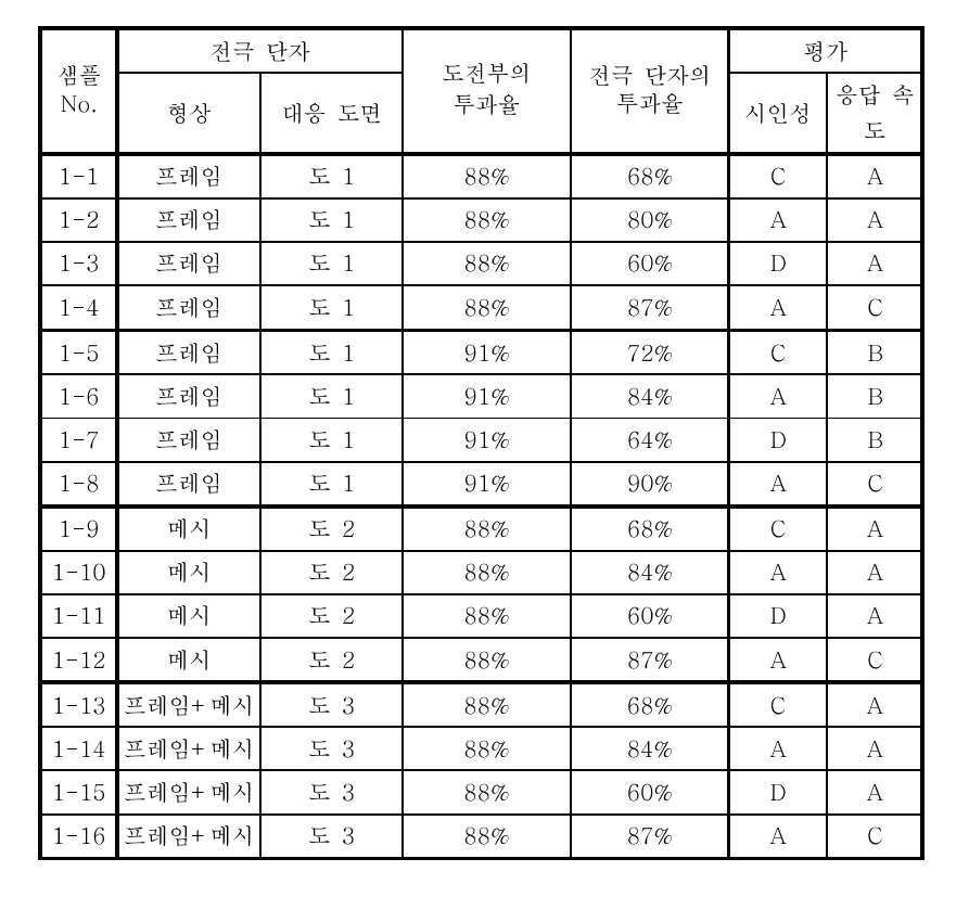
<결과 1><
표 1 로부터 알 수 있듯이, 샘플들 1-1 내지 1-16 중에서 본 발명에 따른 범위 내의 투과율들을 갖는 샘플들은 적정한 시인성을 나타냈다. 또한, 손가락으로 터치 패널들을 터치하여 조작했을 때에, 샘플들 1-1 내지 1-16 중에서 본 발명에 따른 범위 내의 투과율들을 갖는 샘플들은 응답 속도가 빠르고 검출 감도가 우수한 것을 발견하였다. 또, 터치 패널들을 2 개 이상의 지점들에서 터치하고 조작했을 때에, 터치 패널들은 유사하게 적정한 결과들을 나타냈다. 그리하여, 터치 패널들이 멀티터치에도 또한 대응할 수 있음을 확인하였다.As can be seen from Table 1, among the samples 1-1 to 1-16, the samples having transmittances within the range according to the present invention exhibited adequate visibility. Also, when the touch panels were touched with the fingers, the samples 1-1 through 1-16 found that the samples having the transmittances within the range according to the present invention had a fast response speed and excellent detection sensitivity. Also, when the touch panels were touched and manipulated at two or more points, the touch panels similarly displayed reasonable results. Thus, it is confirmed that the touch panels can also cope with multi-touch.
[실험 2][Experiment 2]
(샘플 2-1) 실시예(Sample 2-1) Example
제조된 제 1 도전 시트 (12A) 및 제 2 도전 시트 (12B) 의 도전부들 (제 1 전극 패턴 (16A) 및 제 2 전극 패턴 (16B)) 의 개구율들은 90 % 이다. 제조된 제 1 도전 시트 (12A) 및 제 2 도전 시트 (12B) 의 전극 단자 (60A) 및 전극 단자 (60B) 는 도 5a 및 도 5b 에 도시된 패턴들을 가지며, 개구율들은 70 % 이다.The aperture ratios of the conductive portions (the
(샘플 2-2) 실시예(Sample 2-2) Example
제조된 제 1 도전 시트 (12A) 및 제 2 도전 시트 (12B) 의 전극 단자 (60A) 및 전극 단자 (60B) 의 개구율들을 89.9 % 로 제어한 것 이외에는, 샘플 2-1 과 마찬가지로 샘플 2-2 를 제작하였다.The openings of the
(샘플 2-3) 비교예(Sample 2-3) Comparative Example
제조된 제 1 도전 시트 (12A) 및 제 2 도전 시트 (12B) 의 전극 단자 (60A) 및 전극 단자 (60B) 의 개구율들을 68 % 로 제어한 것 이외에는, 샘플 2-1 과 마찬가지로 샘플 2-3 을 제작하였다.Same as Sample 2-1, except that the aperture ratios of the
(샘플 2-4) 비교예(Sample 2-4) Comparative Example
제조된 제 1 도전 시트 (12A) 및 제 2 도전 시트 (12B) 의 전극 단자 (60A) 및 전극 단자 (60B) 의 개구율들을 90 % 로 제어한 것 이외에는, 샘플 2-1 과 마찬가지로 샘플 2-4 를 제작하였다.The openings of the
(샘플 2-5) 실시예(Sample 2-5) Example
제조된 제 1 도전 시트 (12A) 및 제 2 도전 시트 (12B) 의 도전부들 (제 1 전극 패턴 (16A) 및 제 2 전극 패턴 (16B)) 의 개구율들은 97 % 이다. 제조된 제 1 도전 시트 (12A) 및 제 2 도전 시트 (12B) 의 전극 단자 (60A) 및 전극 단자 (60B) 는 도 5a 및 도 5b 에 도시된 패턴들을 가지며, 개구율들은 77 % 이다.The aperture ratios of the conductive portions (the
(샘플 2-6) 실시예(Sample 2-6) Example
제조된 제 1 도전 시트 (12A) 및 제 2 도전 시트 (12B) 의 전극 단자 (60A) 및 전극 단자 (60B) 의 개구율들을 96.9 % 로 제어한 것 이외에는, 샘플 2-5 와 마찬가지로 샘플 2-6 을 제작하였다.The openings of the
(샘플 2-7) 비교예(Sample 2-7) Comparative Example
제조된 제 1 도전 시트 (12A) 및 제 2 도전 시트 (12B) 의 전극 단자 (60A) 및 전극 단자 (60B) 의 개구율들을 75 % 로 제어한 것 이외에는, 샘플 2-5 와 마찬가지로 샘플 2-7 을 제작하였다.The openings of the
(샘플 2-8) 비교예(Sample 2-8) Comparative Example
제조된 제 1 도전 시트 (12A) 및 제 2 도전 시트 (12B) 의 전극 단자 (60A) 및 전극 단자 (60B) 의 개구율들을 97 % 로 제어한 것 이외에는, 샘플 2-5 와 마찬가지로 샘플 2-8 을 제작하였다.The openings of the
(샘플 2-9) 실시예(Sample 2-9) Example
제조된 제 1 도전 시트 (12A) 및 제 2 도전 시트 (12B) 의 도전부들 (제 1 전극 패턴 (16A) 및 제 2 전극 패턴 (16B)) 의 개구율들은 90 % 이다. 제조된 제 1 도전 시트 (12A) 및 제 2 도전 시트 (12B) 의 전극 단자 (60A) 및 전극 단자 (60B) 는 도 6a 및 도 6b 에 도시된 패턴들을 가지며, 개구율들은 70 % 이다.The aperture ratios of the conductive portions (the
(샘플 2-10) 실시예(Sample 2-10) Example
제조된 제 1 도전 시트 (12A) 및 제 2 도전 시트 (12B) 의 전극 단자 (60A) 및 전극 단자 (60B) 의 개구율들을 89.9 % 로 제어한 것 이외에는, 샘플 2-9 와 마찬가지로 샘플 2-10 을 제작하였다.The openings of the
(샘플 2-11) 비교예(Sample 2-11) Comparative Example
제조된 제 1 도전 시트 (12A) 및 제 2 도전 시트 (12B) 의 전극 단자 (60A) 및 전극 단자 (60B) 의 개구율들을 68 % 로 제어한 것 이외에는, 샘플 2-9 와 마찬가지로 샘플 2-11 을 제작하였다.The openings of the
(샘플 2-12) 비교예(Sample 2-12) Comparative Example
제조된 제 1 도전 시트 (12A) 및 제 2 도전 시트 (12B) 의 전극 단자 (60A) 및 전극 단자 (60B) 의 개구율들을 90 % 로 제어한 것 이외에는, 샘플 2-9 와 마찬가지로 샘플 2-12 을 제작하였다.As in Sample 2-9, except that the aperture ratios of the
(샘플 2-13) 실시예(Sample 2-13) Example
제조된 제 1 도전 시트 (12A) 및 제 2 도전 시트 (12B) 의 도전부들 (제 1 전극 패턴 (16A) 및 제 2 전극 패턴 (16B)) 의 개구율들은 90 % 이다. 제조된 제 1 도전 시트 (12A) 및 제 2 도전 시트 (12B) 의 전극 단자 (60A) 및 전극 단자 (60B) 는 도 7 에 도시된 패턴들을 가지며, 개구율들은 70 % 이다.The aperture ratios of the conductive portions (the
(샘플 2-14) 실시예(Sample 2-14) Example
제조된 제 1 도전 시트 (12A) 및 제 2 도전 시트 (12B) 의 전극 단자 (60A) 및 전극 단자 (60B) 의 개구율들을 89.9 % 로 제어한 것 이외에는, 샘플 2-13 과 마찬가지로 샘플 2-14 를 제작하였다.The openings of the
(샘플 2-15) 비교예(Sample 2-15) Comparative Example
제조된 제 1 도전 시트 (12A) 및 제 2 도전 시트 (12B) 의 전극 단자 (60A) 및 전극 단자 (60B) 의 개구율들을 68 % 로 제어한 것 이외에는, 샘플 2-13 과 마찬가지로 샘플 2-15 를 제작하였다.As in Sample 2-13, except that the aperture ratios of the
(샘플 2-16) 비교예(Sample 2-16) Comparative Example
제조된 제 1 도전 시트 (12A) 및 제 2 도전 시트 (12B) 의 전극 단자 (60A) 및 전극 단자 (60B) 의 개구율들을 90 % 로 제어한 것 이외에는, 샘플 2-13 과 마찬가지로 샘플 2-16 을 제작하였다.As in Sample 2-13, except that the aperture ratios of the
<개구율의 측정>≪ Measurement of aperture ratio &
제 1 도전 시트 (12A) 및 제 2 도전 시트 (12B) 의 개구율들에 대해, KEYENCE CORPORATION 제조의 현미경 VHX-200 을 이용하여 배율 3,000 (3,000 배 파워) 으로 측정하였다.The aperture ratios of the first
<시인성의 평가><Evaluation of visibility>
상기 기재된 샘플들에 관련된 적층 도전 시트들의 각각을 이용하여 투영형 정전용량방식의 터치 패널들을 제조하였다. 각각의 터치 패널을 회전반 상에 설치하고, 액정 표시 장치를 구동하여, 백색을 표시하였다. 이때, 센싱 영역의 전극 단자 근방에서 그림자 (어두워진 부분) 를 인지할 수 있는지의 여부를 육안으로 확인하였다.A projection type capacitive touch panel was manufactured using each of the laminated conductive sheets related to the above described samples. Each of the touch panels was mounted on a rotating panel, and the liquid crystal display device was driven to display white. At this time, whether or not a shadow (darkened portion) could be recognized in the vicinity of the electrode terminal of the sensing region was visually confirmed.
시인성이 우수한 터치 패널을 A 로 평가하고, 시인성이 적정 (양호) 한 터치 패널을 B 로 평가하고, 실용상 시인성이 영향을 받지 않는 터치 패널을 C 로 평가하고, 시인성이 열등한 터치 패널을 D 로 평가하였다.A touch panel having excellent visibility was evaluated with A, a touch panel having good visibility (good) was rated B, and a touch panel having no influence on practical use was evaluated with C. The touch panel having poor visibility was evaluated as D Respectively.
<응답 속도의 평가><Evaluation of response speed>
응답 속도가 우수한 터치 패널을 A 로 평가하고, 응답 속도가 적정한 터치 패널을 B 로 평가하고, 실용상 응답 속도가 문제로 되지 않는 터치 패널을 C 로 평가하고, 응답 속도가 느리고 검출 감도가 열등한 터치 패널을 D 로 평가하였다.A touch panel with an excellent response speed is evaluated by A, a touch panel with an appropriate response speed is evaluated by B, a touch panel whose response speed is not a problem is evaluated by C, a touch with a slow response speed and poor detection sensitivity The panel was rated D.

<결과 2><Result 2>
표 2 로부터 알 수 있듯이, 샘플들 2-1 내지 2-16 중에서 본 발명에 따른 범위 내의 개구율들을 갖는 샘플들은 적정한 시인성을 나타냈다. 또한, 손가락으로 터치 패널들을 터치하여 조작했을 때에, 샘플들 2-1 내지 2-16 중에서 본 발명에 따른 범위 내의 개구율들을 갖는 샘플들은 응답 속도가 빠르고 검출 감도가 우수한 것을 발견하였다. 또, 터치 패널들을 2 개 이상의 지점들에서 터치하고 조작했을 때에, 터치 패널들은 유사하게 적정한 결과들을 나타냈다. 그리하여, 터치 패널들이 멀티터치에도 또한 대응할 수 있음을 확인하였다.As can be seen from Table 2, among the samples 2-1 to 2-16, the samples having the aperture ratios within the range according to the present invention showed adequate visibility. Also, when the touch panels were touched with the fingers and operated, it was found that the samples having the aperture ratios within the range according to the present invention among the samples 2-1 to 2-16 have fast response speed and excellent detection sensitivity. Also, when the touch panels were touched and manipulated at two or more points, the touch panels similarly displayed reasonable results. Thus, it is confirmed that the touch panels can also cope with multi-touch.
본 발명에 따른 도전 시트 및 터치 패널은 상기 기재된 실시형태들에 한정되지 않으며, 본 발명의 요지를 일탈하지 않고서 다양한 구조들을 채택할 수 있음은 물론이다.It is needless to say that the conductive sheet and the touch panel according to the present invention are not limited to the above-described embodiments, and various structures can be adopted without departing from the gist of the present invention.
10 : (터치 패널용) 도전 시트
12A : (제 1) 도전 시트 12B : (제 2) 도전 시트
14A : (제 1) 투명 기재 14B : (제 2) 투명 기재
16A : (제 1) 전극 패턴 16B : (제 2) 전극 패턴
18A : (제 1) 도전 패턴 18B : (제 2) 도전 패턴
20A : (제 1) 비도전 패턴 20B : (제 2) 비도전 패턴
22A : 단선부 22B : 단선부
24A : 격자 24B : 격자
60A : (제 1) 전극 단자 60B : (제 2) 전극 단자
62A : (제 1) 외부 배선 62B : (제 2) 외부 배선
64 : 프레임 형상 66 : 메시 형상
68 : 격자 70 : 조합 패턴10: (for touch panel) Conductive sheet
12A: (first)
14A: (first)
16A: (first)
18A: (first)
20A: (first)
22A:
24A:
60A: (first)
62A: (first)
64: frame shape 66: mesh shape
68: Grid 70: Combination pattern
Claims (12)
상기 전극 패턴의 단부에 전기적으로 접속된 전극 단자를 포함하는 도전 시트로서,
상기 전극 패턴의 투과율이 83 % 이상이며, 상기 전극 패턴의 투과율을 a % 로 나타낼 때에, 상기 전극 단자의 투과율은 (a-20) % 이상 (a-3) % 이하인, 도전 시트.An electrode pattern composed of metal thin wires; And
And an electrode terminal electrically connected to an end of the electrode pattern,
Wherein the electrode pattern has a transmittance of not less than (a-20)% and not more than (a-3)% when the transmittance of the electrode pattern is not less than 83% and the transmittance of the electrode pattern is expressed as a%.
상기 전극 패턴의 단부에 전기적으로 접속된 전극 단자를 포함하는 도전 시트로서,
상기 전극 패턴의 개구율이 90 % 이상이며, 상기 전극 패턴의 개구율을 b % 로 나타낼 때에, 상기 전극 단자의 개구율은 (b-20) % 이상 (b-0.1) % 이하인, 도전 시트.An electrode pattern composed of metal thin wires; And
And an electrode terminal electrically connected to an end of the electrode pattern,
Wherein an opening ratio of the electrode terminal is not less than (b-20)% and not more than (b-0.1)% when the opening ratio of the electrode pattern is 90% or more and the opening ratio of the electrode pattern is b%.
상기 전극 단자는 금속 세선으로 구성된 격자들로 이루어진 메시 형상을 포함하는, 도전 시트.3. The method according to claim 1 or 2,
Wherein the electrode terminal comprises a mesh shape of grids made of metal wires.
상기 금속 세선은 30 ㎛ 이하의 선폭을 갖는, 도전 시트.The method of claim 3,
Wherein the metal thin wire has a line width of 30 mu m or less.
상기 금속 세선은 불투명한 재료로 구성되는, 도전 시트.The method of claim 3,
Wherein the metal thin wire is made of an opaque material.
상기 전극 패턴의 투과율이 83 % 이상이며, 상기 전극 패턴의 투과율을 a % 로 나타낼 때에, 상기 전극 단자의 투과율은 (a-20) % 이상 (a-3) % 이하인, 터치 패널.An electrode pattern provided in the sensing region and composed of metal thin wires; And a conductive sheet provided on an outer side of the sensing region and electrically connected to an end of the electrode pattern,
The transmittance of the electrode terminal is not less than (a-20)% and not more than (a-3)% when the transmittance of the electrode pattern is not less than 83% and the transmittance of the electrode pattern is expressed as a%.
상기 전극 패턴의 개구율이 90 % 이상이며, 상기 전극 패턴의 개구율을 b % 로 나타낼 때에, 상기 전극 단자의 개구율은 (b-20) % 이상 (b-0.1) % 이하인, 터치 패널.An electrode pattern provided in the sensing region and composed of metal thin wires; And a conductive sheet provided on an outer side of the sensing region and electrically connected to an end of the electrode pattern,
Wherein an aperture ratio of the electrode pattern is not less than (b-20)% and not more than (b-0.1)% when the aperture ratio of the electrode pattern is 90% or more and the aperture ratio of the electrode pattern is b%.
상기 전극 패턴의 단부에 전기적으로 접속된 전극 단자를 포함하는 도전 시트로서,
상기 전극 단자는, 금속 세선으로 구성된 프레임 형상을 포함하는, 도전 시트.An electrode pattern composed of metal thin wires; And
And an electrode terminal electrically connected to an end of the electrode pattern,
Wherein the electrode terminal includes a frame shape composed of metal thin wires.
상기 전극 패턴의 세선의 선폭을 a ㎛ 로 나타낼 때에, 상기 전극 단자의 프레임 형상의 선폭 b ㎛ 는 b ≥ 2a 또는 b ≥ a+5 (㎛) 를 만족하는, 도전 시트.9. The method of claim 8,
The line width of the frame shape of the electrode terminal satisfies b? 2a or b? A + 5 (占 퐉) when the line width of the fine line of the electrode pattern is represented by a 占 퐉.
상기 전극 패턴의 세선의 선폭 a ㎛ 는 30 ㎛ 이하인, 도전 시트.10. The method of claim 9,
Wherein a line width of a fine line of the electrode pattern is not more than 30 mu m.
상기 전극 단자의 금속 세선으로 구성된 프레임 형상 내에 제공되고, 금속 세선으로 구성된 격자들로 이루어진 메시 형상을 더 포함하는, 도전 시트.11. The method according to claim 9 or 10,
Further comprising a mesh shape provided in a frame shape composed of metal thin wires of said electrode terminal and made of grids made of metal thin wires.
상기 전극 단자는, 금속 세선으로 구성된 프레임 형상을 포함하는, 터치 패널.An electrode pattern provided in the sensing region and composed of metal thin wires; And a conductive sheet provided on an outer side of the sensing region and electrically connected to an end of the electrode pattern,
Wherein the electrode terminal includes a frame shape composed of metal thin wires.
Applications Claiming Priority (7)
| Application Number | Priority Date | Filing Date | Title |
|---|---|---|---|
| JPJP-P-2011-276069 | 2011-12-16 | ||
| JP2011276069A JP5777251B2 (en) | 2011-12-16 | 2011-12-16 | Conductive sheet for touch panel and touch panel |
| JPJP-P-2011-276070 | 2011-12-16 | ||
| JP2011276070A JP5509186B2 (en) | 2011-12-16 | 2011-12-16 | Touch panel and conductive sheet for touch panel |
| JP2011281926A JP5748647B2 (en) | 2011-12-22 | 2011-12-22 | Conductive sheet and touch panel |
| JPJP-P-2011-281926 | 2011-12-22 | ||
| PCT/JP2012/082030 WO2013089085A1 (en) | 2011-12-16 | 2012-12-11 | Conductive sheet and touch panel |
Related Parent Applications (1)
| Application Number | Title | Priority Date | Filing Date |
|---|---|---|---|
| KR1020147011920A Division KR101451075B1 (en) | 2011-12-16 | 2012-12-11 | Electroconductive sheet and touch panel |
Publications (2)
| Publication Number | Publication Date |
|---|---|
| KR20140090176A true KR20140090176A (en) | 2014-07-16 |
| KR101645828B1 KR101645828B1 (en) | 2016-08-04 |
Family
ID=48612532
Family Applications (2)
| Application Number | Title | Priority Date | Filing Date |
|---|---|---|---|
| KR1020147011932A KR101645828B1 (en) | 2011-12-16 | 2012-12-11 | Electroconductive sheet and touch panel |
| KR1020147011920A KR101451075B1 (en) | 2011-12-16 | 2012-12-11 | Electroconductive sheet and touch panel |
Family Applications After (1)
| Application Number | Title | Priority Date | Filing Date |
|---|---|---|---|
| KR1020147011920A KR101451075B1 (en) | 2011-12-16 | 2012-12-11 | Electroconductive sheet and touch panel |
Country Status (7)
| Country | Link |
|---|---|
| US (2) | US9055680B2 (en) |
| EP (2) | EP2781996B1 (en) |
| KR (2) | KR101645828B1 (en) |
| CN (2) | CN103984461B (en) |
| BR (1) | BR112014010102A8 (en) |
| TW (2) | TWI585631B (en) |
| WO (1) | WO2013089085A1 (en) |
Families Citing this family (36)
| Publication number | Priority date | Publication date | Assignee | Title |
|---|---|---|---|---|
| EP2781996B1 (en) | 2011-12-16 | 2019-12-04 | Fujifilm Corporation | Conductive sheet and touch panel |
| JP5910761B2 (en) * | 2013-01-25 | 2016-04-27 | 凸版印刷株式会社 | Touch panel and display device |
| US20140251672A1 (en) * | 2013-03-05 | 2014-09-11 | Ronald Steven Cok | Micro-channel connection pad |
| TWI498799B (en) * | 2013-03-27 | 2015-09-01 | Innolux Corp | Touch sensing component and electronic device using the smae |
| WO2014185388A1 (en) * | 2013-05-16 | 2014-11-20 | 三菱製紙株式会社 | Conductive pattern and monolayer capacitive touch panel electrode pattern |
| KR102053258B1 (en) * | 2013-07-16 | 2019-12-06 | 엘지이노텍 주식회사 | Touch window |
| CN111309194B (en) * | 2013-10-22 | 2023-09-15 | 富士胶片株式会社 | Electrode for touch panel, and display device |
| KR102191575B1 (en) * | 2014-01-13 | 2020-12-15 | 엘지이노텍 주식회사 | Touch window and display with the same |
| JP6200582B2 (en) | 2014-04-08 | 2017-09-20 | 株式会社フジクラ | Wiring body and wiring board |
| WO2015186276A1 (en) * | 2014-06-02 | 2015-12-10 | 凸版印刷株式会社 | Touch sensor electrode, touch panel, and display device |
| KR101802690B1 (en) * | 2014-06-10 | 2017-11-28 | 후지필름 가부시키가이샤 | Electrically-conductive laminate for touchscreen, touchscreen, and transparent electrically-conductive laminate |
| KR102256461B1 (en) * | 2014-10-10 | 2021-05-26 | 삼성디스플레이 주식회사 | Touch sensor and display including the same |
| KR20170061148A (en) * | 2014-10-28 | 2017-06-02 | 코니카 미놀타 가부시키가이샤 | Pattern, patterned base material, and touch panel |
| JP6422762B2 (en) * | 2014-12-16 | 2018-11-14 | 三菱製紙株式会社 | Light transmissive conductive material |
| EP3176680A4 (en) | 2015-02-27 | 2018-01-17 | Fujikura, Ltd. | Wiring body, wiring substrate, and touch sensor |
| CN106796477B (en) | 2015-02-27 | 2018-05-29 | 株式会社藤仓 | Wiring body, circuit board, Wiring structure body and touch sensor |
| KR102255445B1 (en) * | 2015-03-30 | 2021-05-21 | 동우 화인켐 주식회사 | Touch sensor |
| KR102255415B1 (en) * | 2015-03-30 | 2021-05-21 | 동우 화인켐 주식회사 | Touch sensor |
| KR102372334B1 (en) | 2015-04-14 | 2022-03-08 | 삼성디스플레이 주식회사 | Touch panel |
| JP2016206754A (en) * | 2015-04-16 | 2016-12-08 | 凸版印刷株式会社 | Touch sensor electrode, touch panel, and display device |
| KR102286210B1 (en) * | 2015-05-04 | 2021-08-05 | 엘지이노텍 주식회사 | Touch panel |
| CN107533411B (en) * | 2015-05-04 | 2021-03-16 | Lg伊诺特有限公司 | Touch panel |
| JP6421077B2 (en) * | 2015-05-19 | 2018-11-07 | 富士フイルム株式会社 | Antenna manufacturing method and touch sensor |
| TWI610206B (en) | 2015-06-22 | 2018-01-01 | Fujikura Ltd | Wiring body, wiring board, and touch sensor |
| JP6755000B2 (en) * | 2016-03-28 | 2020-09-16 | パナソニックIpマネジメント株式会社 | Touch panel sensor members and touch panel |
| US10126899B2 (en) | 2016-04-04 | 2018-11-13 | Japan Display Inc. | Detection device and display device |
| JP6744169B2 (en) * | 2016-04-04 | 2020-08-19 | 株式会社ジャパンディスプレイ | Detection device and display device |
| WO2018146963A1 (en) * | 2017-02-09 | 2018-08-16 | コニカミノルタ株式会社 | Touch screen and method for manufacturing touch screen |
| CN109558024A (en) | 2017-09-27 | 2019-04-02 | 京东方科技集团股份有限公司 | Display device, touch panel and its manufacturing method, driving method |
| JP6886907B2 (en) | 2017-10-31 | 2021-06-16 | 日本航空電子工業株式会社 | Touch panel and touch panel production method |
| CN109976566B (en) * | 2018-03-23 | 2021-05-18 | 京东方科技集团股份有限公司 | Touch structure, touch substrate, manufacturing method of touch substrate and display device |
| JP7115036B2 (en) * | 2018-05-25 | 2022-08-09 | ウシオ電機株式会社 | excimer lamp |
| JP6658800B2 (en) * | 2018-06-12 | 2020-03-04 | コニカミノルタ株式会社 | Functional fine wire pattern, substrate with transparent conductive film, device and electronic equipment |
| CN108897463B (en) * | 2018-07-06 | 2021-08-06 | 广州国显科技有限公司 | Touch device and display device |
| CN113518966B (en) * | 2020-02-12 | 2024-03-19 | 京东方科技集团股份有限公司 | Touch display substrate and touch display device |
| US11157122B1 (en) * | 2020-06-03 | 2021-10-26 | Futuretech Capital, Inc. | Method to design low visibility metal mesh touch sensor |
Citations (10)
| Publication number | Priority date | Publication date | Assignee | Title |
|---|---|---|---|---|
| US5113041A (en) | 1990-12-28 | 1992-05-12 | At&T Bell Laboratories | Information processing |
| JPH05224818A (en) | 1992-02-10 | 1993-09-03 | Matsushita Electric Ind Co Ltd | Touch panel device |
| WO1995027334A1 (en) | 1994-04-05 | 1995-10-12 | Ronald Peter Binstead | Multiple input proximity detector and touchpad system |
| WO1997018508A1 (en) | 1995-11-13 | 1997-05-22 | Synaptics, Inc. | Pressure sensitive scrollbar feature |
| JP2003099185A (en) | 2001-09-20 | 2003-04-04 | Alps Electric Co Ltd | Input device |
| US20040229028A1 (en) | 2002-12-27 | 2004-11-18 | Fuji Photo Film Co., Ltd. | Method for producing light-transmitting electromagnetic wave-shielding film, light-transmitting electromagnetic wave-shielding film and plasma display panel using the shielding film |
| US20040239650A1 (en) | 2003-06-02 | 2004-12-02 | Mackey Bob Lee | Sensor patterns for a capacitive sensing apparatus |
| WO2006001461A1 (en) | 2004-06-23 | 2006-01-05 | Fuji Photo Film Co., Ltd. | Transparent electromagnetic shielding film and method for producing same |
| US7202859B1 (en) | 2002-08-09 | 2007-04-10 | Synaptics, Inc. | Capacitive sensing pattern |
| KR20110130343A (en) * | 2010-05-27 | 2011-12-05 | 후지필름 가부시키가이샤 | Conductive sheet and capacitive touch panel |
Family Cites Families (33)
| Publication number | Priority date | Publication date | Assignee | Title |
|---|---|---|---|---|
| WO2004008423A1 (en) * | 2002-07-12 | 2004-01-22 | Sharp Kabushiki Kaisha | Wiring structure, display apparatus, and active device substrate |
| JP4610416B2 (en) * | 2005-06-10 | 2011-01-12 | 日本写真印刷株式会社 | Capacitive touch panel |
| US8264466B2 (en) * | 2006-03-31 | 2012-09-11 | 3M Innovative Properties Company | Touch screen having reduced visibility transparent conductor pattern |
| JP4915954B2 (en) * | 2007-11-27 | 2012-04-11 | グンゼ株式会社 | Touch panel and touch panel device using the touch panel |
| CN102016768B (en) * | 2008-02-28 | 2014-11-19 | 3M创新有限公司 | Touch screen sensor having varying sheet resistance |
| EP3614418B1 (en) * | 2008-02-28 | 2023-11-01 | 3M Innovative Properties Company | Touch screen sensor |
| JP2011517367A (en) * | 2008-02-28 | 2011-06-02 | スリーエム イノベイティブ プロパティズ カンパニー | Method for patterning a conductor on a substrate |
| US8284332B2 (en) * | 2008-08-01 | 2012-10-09 | 3M Innovative Properties Company | Touch screen sensor with low visibility conductors |
| EP2113827B8 (en) * | 2008-04-30 | 2018-09-19 | InnoLux Corporation | Touch input device |
| JP5253288B2 (en) * | 2009-05-08 | 2013-07-31 | グンゼ株式会社 | Planar body and touch switch |
| KR101329638B1 (en) * | 2008-07-31 | 2013-11-14 | 군제 가부시키가이샤 | Planar element, and touch switch |
| US9244568B2 (en) | 2008-11-15 | 2016-01-26 | Atmel Corporation | Touch screen sensor |
| KR100909265B1 (en) * | 2009-02-23 | 2009-07-27 | (주)이엔에이치테크 | Manufacturing method of electrostatic capacity type touch screen panel |
| DE102009014757A1 (en) * | 2009-03-27 | 2010-10-07 | Polyic Gmbh & Co. Kg | Electrical functional layer, manufacturing method and use thereof |
| WO2010114084A1 (en) * | 2009-03-30 | 2010-10-07 | リンテック株式会社 | Electrically-conductive transparent film |
| WO2010113970A1 (en) * | 2009-03-31 | 2010-10-07 | 帝人株式会社 | Transparent conductive laminate and transparent touch panel |
| JP2010251230A (en) * | 2009-04-20 | 2010-11-04 | Fujifilm Corp | Electric heating window glass |
| US20110007011A1 (en) * | 2009-07-13 | 2011-01-13 | Ocular Lcd Inc. | Capacitive touch screen with a mesh electrode |
| CN102598891B (en) * | 2009-07-16 | 2015-11-25 | Lg化学株式会社 | Electric conductor and manufacture method thereof |
| JP5298352B2 (en) * | 2009-09-16 | 2013-09-25 | 株式会社トプコン | Optical structure image observation device and endoscope device |
| US20120231248A1 (en) * | 2009-11-11 | 2012-09-13 | Toray Industries, Inc. | Conductive laminate and method of producing the same |
| JP2012014669A (en) * | 2009-11-20 | 2012-01-19 | Fujifilm Corp | Conductive sheet, method of using conductive sheet and electrostatic capacitive touch panel |
| JP4820451B2 (en) | 2009-11-20 | 2011-11-24 | 富士フイルム株式会社 | Conductive sheet, method of using conductive sheet, and touch panel |
| JP2011113149A (en) | 2009-11-24 | 2011-06-09 | Fujifilm Corp | Conductive sheet, use method for the same and capacitance type touch panel |
| KR101660564B1 (en) | 2009-11-24 | 2016-09-27 | 후지필름 가부시키가이샤 | Conductive sheet, usage method of conductive sheet and capacitive type touch panel |
| US8432678B2 (en) * | 2010-01-06 | 2013-04-30 | Apple Inc. | Component assembly |
| JP5638399B2 (en) * | 2010-01-28 | 2014-12-10 | 富士フイルム株式会社 | Conductive sheet, method of using conductive sheet, and capacitive touch panel |
| JP5123370B2 (en) | 2010-01-28 | 2013-01-23 | 富士フイルム株式会社 | Conductive sheet, method of using conductive sheet, and capacitive touch panel |
| JP5613448B2 (en) | 2010-04-30 | 2014-10-22 | 富士フイルム株式会社 | Touch panel and conductive sheet |
| KR101726623B1 (en) * | 2010-03-16 | 2017-04-14 | 엘지디스플레이 주식회사 | Touch Panel |
| TWI404996B (en) * | 2010-12-31 | 2013-08-11 | Au Optronics Corp | Method of manufacturing a touch panel and touch panel |
| TWM415361U (en) * | 2011-04-22 | 2011-11-01 | Young Lighting Technology Corp | Touch device |
| EP2781996B1 (en) | 2011-12-16 | 2019-12-04 | Fujifilm Corporation | Conductive sheet and touch panel |
-
2012
- 2012-12-11 EP EP14171329.7A patent/EP2781996B1/en active Active
- 2012-12-11 WO PCT/JP2012/082030 patent/WO2013089085A1/en active Application Filing
- 2012-12-11 KR KR1020147011932A patent/KR101645828B1/en active IP Right Grant
- 2012-12-11 CN CN201410236276.XA patent/CN103984461B/en active Active
- 2012-12-11 CN CN201280053290.5A patent/CN103907082B/en active Active
- 2012-12-11 EP EP12857606.3A patent/EP2765490B1/en not_active Not-in-force
- 2012-12-11 BR BR112014010102A patent/BR112014010102A8/en not_active Application Discontinuation
- 2012-12-11 KR KR1020147011920A patent/KR101451075B1/en active IP Right Grant
- 2012-12-14 TW TW103114610A patent/TWI585631B/en active
- 2012-12-14 TW TW101147588A patent/TWI537779B/en active
-
2014
- 2014-04-29 US US14/264,879 patent/US9055680B2/en active Active
- 2014-05-07 US US14/271,512 patent/US9078364B2/en active Active
Patent Citations (10)
| Publication number | Priority date | Publication date | Assignee | Title |
|---|---|---|---|---|
| US5113041A (en) | 1990-12-28 | 1992-05-12 | At&T Bell Laboratories | Information processing |
| JPH05224818A (en) | 1992-02-10 | 1993-09-03 | Matsushita Electric Ind Co Ltd | Touch panel device |
| WO1995027334A1 (en) | 1994-04-05 | 1995-10-12 | Ronald Peter Binstead | Multiple input proximity detector and touchpad system |
| WO1997018508A1 (en) | 1995-11-13 | 1997-05-22 | Synaptics, Inc. | Pressure sensitive scrollbar feature |
| JP2003099185A (en) | 2001-09-20 | 2003-04-04 | Alps Electric Co Ltd | Input device |
| US7202859B1 (en) | 2002-08-09 | 2007-04-10 | Synaptics, Inc. | Capacitive sensing pattern |
| US20040229028A1 (en) | 2002-12-27 | 2004-11-18 | Fuji Photo Film Co., Ltd. | Method for producing light-transmitting electromagnetic wave-shielding film, light-transmitting electromagnetic wave-shielding film and plasma display panel using the shielding film |
| US20040239650A1 (en) | 2003-06-02 | 2004-12-02 | Mackey Bob Lee | Sensor patterns for a capacitive sensing apparatus |
| WO2006001461A1 (en) | 2004-06-23 | 2006-01-05 | Fuji Photo Film Co., Ltd. | Transparent electromagnetic shielding film and method for producing same |
| KR20110130343A (en) * | 2010-05-27 | 2011-12-05 | 후지필름 가부시키가이샤 | Conductive sheet and capacitive touch panel |
Also Published As
| Publication number | Publication date |
|---|---|
| EP2765490A4 (en) | 2015-05-06 |
| EP2781996A2 (en) | 2014-09-24 |
| EP2781996B1 (en) | 2019-12-04 |
| KR101645828B1 (en) | 2016-08-04 |
| US20140238730A1 (en) | 2014-08-28 |
| US9078364B2 (en) | 2015-07-07 |
| CN103907082A (en) | 2014-07-02 |
| EP2781996A3 (en) | 2015-03-04 |
| BR112014010102A2 (en) | 2017-06-13 |
| KR101451075B1 (en) | 2014-10-15 |
| TWI585631B (en) | 2017-06-01 |
| CN103984461A (en) | 2014-08-13 |
| KR20140063900A (en) | 2014-05-27 |
| CN103907082B (en) | 2016-09-21 |
| EP2765490B1 (en) | 2017-06-07 |
| TW201432527A (en) | 2014-08-16 |
| EP2765490A1 (en) | 2014-08-13 |
| WO2013089085A1 (en) | 2013-06-20 |
| US20140231120A1 (en) | 2014-08-21 |
| CN103984461B (en) | 2017-09-15 |
| US9055680B2 (en) | 2015-06-09 |
| TW201327315A (en) | 2013-07-01 |
| BR112014010102A8 (en) | 2017-06-20 |
| TWI537779B (en) | 2016-06-11 |
Similar Documents
| Publication | Publication Date | Title |
|---|---|---|
| KR101645828B1 (en) | Electroconductive sheet and touch panel | |
| KR101634468B1 (en) | Conductive sheet and touch panel | |
| KR101624391B1 (en) | Electroconductive sheet and touch panel | |
| KR101641761B1 (en) | Conductive sheet and touch panel | |
| KR101651723B1 (en) | Conductive sheet and touch panel | |
| KR101641760B1 (en) | Conductive sheet and touch panel | |
| KR101570595B1 (en) | Conductive sheet and touch panel | |
| JP5748647B2 (en) | Conductive sheet and touch panel | |
| JP5638027B2 (en) | Conductive sheet and capacitive touch panel | |
| JP5822395B2 (en) | Conductive sheet, inspection method and manufacturing method thereof | |
| JP5509186B2 (en) | Touch panel and conductive sheet for touch panel | |
| KR20120116920A (en) | Conductive sheet, usage method of conductive sheet and capacitive type touch panel | |
| JP5850967B2 (en) | Conductive sheet for touch panel and touch panel | |
| JP5777251B2 (en) | Conductive sheet for touch panel and touch panel | |
| WO2014061591A1 (en) | Electrically conductive sheet, and touch panel |
Legal Events
| Date | Code | Title | Description |
|---|---|---|---|
| A107 | Divisional application of patent | ||
| A201 | Request for examination | ||
| E902 | Notification of reason for refusal | ||
| E701 | Decision to grant or registration of patent right | ||
| FPAY | Annual fee payment |
Payment date: 20190722 Year of fee payment: 4 |