JP4820451B2 - Conductive sheet, method of using conductive sheet, and touch panel - Google Patents
Conductive sheet, method of using conductive sheet, and touch panel Download PDFInfo
- Publication number
- JP4820451B2 JP4820451B2 JP2010120331A JP2010120331A JP4820451B2 JP 4820451 B2 JP4820451 B2 JP 4820451B2 JP 2010120331 A JP2010120331 A JP 2010120331A JP 2010120331 A JP2010120331 A JP 2010120331A JP 4820451 B2 JP4820451 B2 JP 4820451B2
- Authority
- JP
- Japan
- Prior art keywords
- lattices
- conductive sheet
- conductive
- lattice
- small
- Prior art date
- Legal status (The legal status is an assumption and is not a legal conclusion. Google has not performed a legal analysis and makes no representation as to the accuracy of the status listed.)
- Active
Links
Images


Classifications
-
- G—PHYSICS
- G06—COMPUTING; CALCULATING OR COUNTING
- G06F—ELECTRIC DIGITAL DATA PROCESSING
- G06F3/00—Input arrangements for transferring data to be processed into a form capable of being handled by the computer; Output arrangements for transferring data from processing unit to output unit, e.g. interface arrangements
- G06F3/01—Input arrangements or combined input and output arrangements for interaction between user and computer
- G06F3/03—Arrangements for converting the position or the displacement of a member into a coded form
- G06F3/041—Digitisers, e.g. for touch screens or touch pads, characterised by the transducing means
- G06F3/044—Digitisers, e.g. for touch screens or touch pads, characterised by the transducing means by capacitive means
- G06F3/0445—Digitisers, e.g. for touch screens or touch pads, characterised by the transducing means by capacitive means using two or more layers of sensing electrodes, e.g. using two layers of electrodes separated by a dielectric layer
-
- G—PHYSICS
- G06—COMPUTING; CALCULATING OR COUNTING
- G06F—ELECTRIC DIGITAL DATA PROCESSING
- G06F3/00—Input arrangements for transferring data to be processed into a form capable of being handled by the computer; Output arrangements for transferring data from processing unit to output unit, e.g. interface arrangements
- G06F3/01—Input arrangements or combined input and output arrangements for interaction between user and computer
- G06F3/03—Arrangements for converting the position or the displacement of a member into a coded form
- G06F3/041—Digitisers, e.g. for touch screens or touch pads, characterised by the transducing means
- G06F3/044—Digitisers, e.g. for touch screens or touch pads, characterised by the transducing means by capacitive means
- G06F3/0446—Digitisers, e.g. for touch screens or touch pads, characterised by the transducing means by capacitive means using a grid-like structure of electrodes in at least two directions, e.g. using row and column electrodes
-
- G—PHYSICS
- G06—COMPUTING; CALCULATING OR COUNTING
- G06F—ELECTRIC DIGITAL DATA PROCESSING
- G06F2203/00—Indexing scheme relating to G06F3/00 - G06F3/048
- G06F2203/041—Indexing scheme relating to G06F3/041 - G06F3/045
- G06F2203/04112—Electrode mesh in capacitive digitiser: electrode for touch sensing is formed of a mesh of very fine, normally metallic, interconnected lines that are almost invisible to see. This provides a quite large but transparent electrode surface, without need for ITO or similar transparent conductive material
-
- G—PHYSICS
- G06—COMPUTING; CALCULATING OR COUNTING
- G06F—ELECTRIC DIGITAL DATA PROCESSING
- G06F3/00—Input arrangements for transferring data to be processed into a form capable of being handled by the computer; Output arrangements for transferring data from processing unit to output unit, e.g. interface arrangements
- G06F3/01—Input arrangements or combined input and output arrangements for interaction between user and computer
- G06F3/03—Arrangements for converting the position or the displacement of a member into a coded form
- G06F3/041—Digitisers, e.g. for touch screens or touch pads, characterised by the transducing means
- G06F3/0412—Digitisers structurally integrated in a display
Landscapes
- Engineering & Computer Science (AREA)
- General Engineering & Computer Science (AREA)
- Theoretical Computer Science (AREA)
- Human Computer Interaction (AREA)
- Physics & Mathematics (AREA)
- General Physics & Mathematics (AREA)
- Position Input By Displaying (AREA)
- Non-Insulated Conductors (AREA)
Description
本発明は、導電シート、導電シートの使用方法及びタッチパルに関し、例えば投影型静電容量方式のタッチパネルに用いて好適な導電シート、導電シートの使用方法及びタッチパネルに関する。 The present invention, the conductive sheet, relates Usage及beauty data Tchiparu conductive sheet, for example, projective capacitive suitable conductive sheet using the touch panel, to a method及Beauty capacitor touch panel using the conductive sheet.
一般に、静電容量方式のタッチパネルは、人間の指先と導電膜との間での静電容量の変化を捉えて指先の位置を検出する位置入力装置であるが、この静電容量方式のタッチパネルとしては、表面型と投影型とがある。表面型は、構造が簡便ではあるが、同時に2点以上の接触(マルチタッチ)を検知することができない。一方、投影型は、例えば液晶表示装置の画素構成のように、多数の電極がマトリクス状に配列して構成され、より具体的には、垂直方向に並ぶ複数の電極が直列に接続された複数の第1電極群が水平方向に配列され、水平方向に並ぶ複数の電極が直列に接続された複数の第2電極群が垂直方向に配列されて構成され、複数の第1電極群及び複数の第2電極群で容量変化を順次検出していくことで、マルチタッチが検出できる構成となっている。この投影型静電容量方式のタッチパネルの先行技術として例えば特許文献1記載の静電容量型入力装置が挙げられる。 In general, a capacitive touch panel is a position input device that detects a fingertip position by detecting a change in capacitance between a human fingertip and a conductive film. There are surface type and projection type. The surface type has a simple structure, but cannot detect two or more contacts (multi-touch) at the same time. On the other hand, the projection type has a configuration in which a large number of electrodes are arranged in a matrix, for example, like a pixel configuration of a liquid crystal display device, and more specifically, a plurality of electrodes in which a plurality of electrodes arranged in the vertical direction are connected in series. The first electrode group is arranged in the horizontal direction, and a plurality of second electrode groups in which a plurality of electrodes arranged in the horizontal direction are connected in series are arranged in the vertical direction. Multi-touch can be detected by sequentially detecting capacitance changes with the second electrode group. As a prior art of this projected capacitive touch panel, for example, a capacitive input device described in Patent Document 1 can be cited.
しかしながら、特許文献1に記載の静電容量型入力装置は、基体の一主面に第1電極群及び第2電極群を形成するようにしているため、第1電極群と第2電極群との短絡防止を目的とした隙間を形成しなければならず、指先の位置の検知精度が劣るという問題がある。また、第1電極群と第2電極群とが交差する部分(交差部)が短絡しないように、例えば第1電極群を構成する電極の接続部上に絶縁層を介して第2電極群を構成する電極の接続部を形成するようにしており、その結果、各交差部が局部的に厚く形成されてしまい、タッチパネル面を見たときに、各交差部が斑点(黒い斑点)として表示され、視認性が著しく劣化するという問題もある。しかも、絶縁層並びに絶縁層上に接続部を形成するためのマスクパターンが必要になることから、製造工程が複雑になり、製造コストが高価格化するという問題がある。 However, since the capacitance-type input device described in Patent Document 1 forms the first electrode group and the second electrode group on one main surface of the substrate, the first electrode group, the second electrode group, Therefore, there is a problem that the detection accuracy of the position of the fingertip is inferior. Further, for example, the second electrode group is formed on the connection portion of the electrodes constituting the first electrode group via an insulating layer so that the portion (intersection) where the first electrode group and the second electrode group intersect is not short-circuited. As a result, each intersection is formed thick locally, and when the touch panel surface is viewed, each intersection is displayed as a spot (black spot). There is also a problem that the visibility is remarkably deteriorated. In addition, since an insulating layer and a mask pattern for forming a connection portion on the insulating layer are required, there is a problem that the manufacturing process becomes complicated and the manufacturing cost increases.
そこで、透明基板の一主面に第1電極群を形成し、透明基板の他主面に第2電極群を形成することが考えられる。
しかし、将来的な観点から見ると、以下のような問題が生じるおそれがある。現在、投影型静電容量方式のタッチパネルは、PDA(携帯情報端末)や携帯電話等の小サイズへの適用が主となっているが、パーソナルコンピュータ(パソコン)用のオペレーションシステム(OS)がマルチタッチ方式を標準対応するようになったことから、パソコン用ディスプレイ等への適用による大サイズ化が進むと考えられる。
Therefore, it is conceivable to form the first electrode group on one main surface of the transparent substrate and form the second electrode group on the other main surface of the transparent substrate.
However, from the perspective of the future, the following problems may occur. At present, the projected capacitive touch panel is mainly applied to a small size such as a PDA (personal digital assistant) or a mobile phone, but an operation system (OS) for a personal computer (personal computer) is multi-purpose. Since the touch system is now available as a standard, it is thought that the size will increase due to the application to personal computer displays.
このような将来の動向において、従来の電極は、ITO(酸化インジウムスズ)を用いていることから、抵抗が大きく(数10オーム/sq.)、適用サイズが大きくなるにつれて、電極間の電流の伝達速度が遅くなり、応答速度(指先を接触してからその位置を検出するまでの時間)が遅くなるという問題がある。 In such a future trend, since the conventional electrode uses ITO (indium tin oxide), the resistance increases (several tens of ohms / sq.), And as the application size increases, the current between the electrodes increases. There is a problem that the transmission speed becomes slow and the response speed (the time from when the fingertip is touched until the position is detected) becomes slow.
本発明はこのような課題を考慮してなされたものであり、基体上に形成される透明導電パターンの低抵抗化を図ることができると共に、視認性も向上させることができ、例えば投影型静電容量方式のタッチパネルに用いて好適な導電シート及び導電シートの使用方法を提供することを目的とする。 The present invention has been made in consideration of such problems, and can reduce the resistance of the transparent conductive pattern formed on the substrate and improve the visibility. It is an object to provide a conductive sheet suitable for use in a capacitive touch panel and a method of using the conductive sheet.
また、本発明の他の目的は、基体上に形成される透明導電パターンの低抵抗化を図ることができると共に、視認性も向上させることができ、例えば投影型静電容量方式のタッチパネルの大サイズ化にも対応させることができるタッチパネルを提供することを目的とする。 Another object of the present invention is to reduce the resistance of the transparent conductive pattern formed on the substrate and to improve the visibility. For example, a large projection capacitive touch panel can be used. An object of the present invention is to provide a touch panel that can be adapted to size.
[1] 第1の本発明に係る導電シートは、基体上に、2以上の導電性の大格子と、隣接する前記大格子間を電気的に接続する接続部とが形成され、各前記大格子は、それぞれ2以上の小格子が組み合わされて構成され、前記接続部は、前記小格子のn倍(nは1より大きい実数)のピッチを有する1以上の中格子が配置されて構成されていることを特徴とする。
[2] 第1の本発明において、前記接続部は、複数の前記中格子がジグザグ状に配列された形状を有することを特徴とする。
[3] 第1の本発明において、前記接続部は、1つの前記小格子とL字状の空間が形成された複数の前記中格子を有することを特徴とする。
[4] 第1の本発明において、前記接続部は、1つの前記小格子とL字状の空間が形成された第1中格子と、4つ分の前記小格子をマトリクス状に配列し、中央の十字を取り外した形状を有する第2中格子が直列に接続されて構成されていることを特徴とする。
[5] 第1の本発明において、前記中格子の配列ピッチは、前記小格子の配列ピッチの1〜10倍であることを特徴とする。
[6] 第1の本発明において、前記小格子の配列ピッチをPs、前記中格子の配列ピッチをPmとしたとき、Pm=2×Psを満足することを特徴とする。
[7] 第1の本発明において、2以上の前記大格子が前記接続部を介して一方向に配列されていることを特徴とする。
[8] 第1の本発明において、2以上の前記大格子が前記接続部を介して第1方向に配列されて1つの透明導電パターンが構成され、2以上の前記透明導電パターンが前記第1方向と直交する第2方向に配列され、隣接する前記透明導電パターン間は電気的に絶縁された絶縁部が配されていることを特徴とする。
[9] 第2の本発明に係る導電シートは、基体の一方の主面に、2以上の導電性の第1大格子と、隣接する前記第1大格子間を電気的に接続する第1接続部とが形成され、前記基体の他方の主面に、2以上の導電性の第2大格子と、隣接する前記第2大格子間を電気的に接続する第2接続部とが形成され、各前記第1大格子及び各前記第2大格子は、それぞれ2以上の小格子が組み合わされて構成され、前記第1接続部及び前記第2接続部は、それぞれ前記小格子のn倍(nは1より大きい実数)のピッチを有する1以上の中格子が配置されて構成されていることを特徴とする。
[10] 第2の本発明において、2以上の前記第1大格子が前記第1接続部を介して第1方向に配列されて1つの第1透明導電パターンが構成され、2以上の前記第2大格子が前記第2接続部を介して前記第1方向と直交する第2方向に配列されて1つの第2透明導電パターンが構成され、2以上の前記第1透明導電パターンが前記第2方向に配列され、2以上の前記第2透明導電パターンが前記第1方向に配列され、隣接する前記第1透明導電パターン間は電気的に絶縁された第1絶縁部が配され、隣接する前記第2透明導電パターン間は電気的に絶縁された第2絶縁部が配され、前記第1接続部と前記第2接続部とが前記基体を間に挟んで対向し、前記第1絶縁部と前記第2絶縁部とが前記基体を間に挟んで対向していることを特徴とする。
[11] 第2の本発明において、前記第1絶縁部と前記第2絶縁部とが前記基体を間に挟んで対向する部分は、前記小格子が2以上配列された大きさの開口が形成された形態を有することを特徴とする。
[12] 第2の本発明において、前記部分は、前記中格子1つ分の大きさの開口が形成された形態を有することを特徴とする。
[13] 第2の本発明において、前記部分は、複数の前記小格子がほぼ十字形状に配列された大きさの開口が形成された形態を有することを特徴とする。
[14] 第2の本発明において、前記第1大格子のうち、第1の辺は、該第1の辺に沿って連続する直線部から多数の針状の線がくし歯状に張り出した形態を有し、前記第1の辺と対向する第2の辺は、該第2の辺に沿って連続する直線部が形成された形態を有し、前記第2大格子のうち、前記基体を介して前記第1大格子の前記第1の辺と対向する第3の辺は、該第3の辺に沿って連続する直線部が形成された形態を有し、前記基体を介して前記第1大格子の前記第2の辺と対向する第4の辺は、該第1の辺に沿って連続する直線部から多数の針状の線がくし歯状に張り出した形態を有することを特徴とする。
[15] 第2の本発明において、前記小格子は正方形状であることを特徴とする。
[16] 第3の本発明に係る導電シートの使用方法は、2以上の導電性の第1大格子と、隣接する前記第1大格子間を電気的に接続する第1接続部とが形成され、各前記第1大格子は、それぞれ2以上の小格子が組み合わされて構成され、前記第1接続部は、それぞれ前記小格子のn倍(nは1より大きい実数)のピッチを有する1以上の中格子が配置されて構成された第1導電シートと、2以上の導電性の第2大格子と、隣接する前記第2大格子間を電気的に接続する第2接続部とが形成され、各前記第2大格子は、それぞれ2以上の小格子が組み合わされて構成され、前記第2接続部は、それぞれ前記小格子のn倍(nは1より大きい実数)のピッチを有する1以上の中格子が配置されて構成された第2導電シートとを使用する導電シートの使用方法であって、前記第1導電シートは、2以上の前記第1大格子が前記第1接続部を介して第1方向に配列されて1つの第1透明導電パターンが構成され、前記第2導電シートは、2以上の前記第2大格子が前記第2接続部を介して前記第1方向と直交する第2方向に配列されて1つの第2透明導電パターンが構成され、前記第1導電シートと前記第2導電シートとを組み合わせることで、前記第1導電シートの前記第1接続部と前記第2導電シートの前記第2接続部とが組み合わさって前記小格子の配列を形成するように配置されることを特徴とする。
[17] 第4の本発明に係る静電容量方式タッチパネルは、第2の本発明に係る導電シートを有することを特徴とする。
[1] In the conductive sheet according to the first aspect of the present invention, two or more conductive large lattices and a connection portion for electrically connecting the adjacent large lattices are formed on a base. Each of the lattices is formed by combining two or more small lattices, and the connection portion is formed by arranging one or more medium lattices having a pitch n times (n is a real number larger than 1) the small lattices. It is characterized by.
[2] In the first aspect of the present invention, the connecting portion has a shape in which a plurality of the intermediate lattices are arranged in a zigzag shape.
[3] In the first aspect of the present invention, the connecting portion includes a plurality of the intermediate lattices in which one small lattice and an L-shaped space are formed.
[4] In the first aspect of the present invention, the connecting portion arranges one small lattice and a first medium lattice in which an L-shaped space is formed, and four small lattices in a matrix, A second intermediate lattice having a shape obtained by removing the central cross is connected in series.
[5] In the first aspect of the present invention, the arrangement pitch of the medium lattice is 1 to 10 times the arrangement pitch of the small lattice.
[6] In the first aspect of the present invention, when the arrangement pitch of the small lattices is Ps and the arrangement pitch of the medium lattices is Pm, Pm = 2 × Ps is satisfied.
[7] The first aspect of the present invention is characterized in that two or more large lattices are arranged in one direction via the connection portion.
[8] In the first aspect of the present invention, two or more of the large lattices are arranged in the first direction via the connecting portion to constitute one transparent conductive pattern, and two or more of the transparent conductive patterns are the first. An insulating part arranged in a second direction orthogonal to the direction and being electrically insulated is disposed between the adjacent transparent conductive patterns.
[9] A conductive sheet according to a second aspect of the present invention is a first sheet that electrically connects two or more conductive first large lattices and the adjacent first large lattices to one main surface of the substrate. And a second connecting portion that electrically connects two or more conductive second large lattices and the adjacent second large lattices is formed on the other main surface of the base body. In addition, each of the first large lattice and each of the second large lattices is configured by combining two or more small lattices, and each of the first connection portion and the second connection portion is n times as large as the small lattice ( It is characterized in that one or more medium lattices having a pitch (n is a real number larger than 1) are arranged.
[10] In the second aspect of the present invention, two or more first large lattices are arranged in the first direction via the first connection portion to form one first transparent conductive pattern, and two or more first transparent lattices are formed. Two large lattices are arranged in a second direction orthogonal to the first direction via the second connection portion to constitute one second transparent conductive pattern, and two or more first transparent conductive patterns are the second Two or more second transparent conductive patterns arranged in a direction are arranged in the first direction, and between the adjacent first transparent conductive patterns, an electrically insulated first insulating portion is arranged, and the adjacent A second insulating portion that is electrically insulated is disposed between the second transparent conductive patterns, the first connecting portion and the second connecting portion are opposed to each other with the base interposed therebetween, and the first insulating portion The second insulating portion is opposed to the base with the base interposed therebetween. The
[11] In the second aspect of the present invention, an opening having a size in which two or more small lattices are arranged is formed in a portion where the first insulating portion and the second insulating portion face each other with the base interposed therebetween. It has the form which was made.
[12] In the second aspect of the present invention, the portion has a form in which an opening having a size corresponding to one of the medium lattices is formed.
[13] In the second aspect of the present invention, the portion has a form in which an opening having a size in which the plurality of small lattices are arranged in a substantially cross shape is formed.
[14] In the second aspect of the present invention, the first side of the first large lattice has a shape in which a large number of needle-like lines project in a comb-tooth shape from a linear portion continuous along the first side. And the second side opposite to the first side has a form in which a linear portion continuous along the second side is formed, and the base of the second large lattice is The third side facing the first side of the first large lattice has a form in which a linear portion continuous along the third side is formed, and the first side through the base body The fourth side opposite to the second side of one large lattice has a form in which a large number of needle-like lines project in a comb-tooth shape from a linear portion continuous along the first side. To do.
[15] In the second aspect of the present invention, the small lattice has a square shape.
[16] The method of using the conductive sheet according to the third aspect of the present invention includes two or more conductive first large lattices and a first connection portion that electrically connects the adjacent first large lattices. Each of the first large lattices is configured by combining two or more small lattices, and each of the first connecting portions has a pitch n times (n is a real number larger than 1) as the small lattice. A first conductive sheet configured by arranging the above-described middle grids, two or more conductive second large grids, and a second connection portion that electrically connects the adjacent second large grids are formed. Each of the second large lattices is configured by combining two or more small lattices, and each of the second connecting portions has a pitch n times (n is a real number greater than 1) pitch of the small lattice. A conductive sheet using the second conductive sheet having the above-described middle grid disposed thereon Wherein the first conductive sheet has two or more first large lattices arranged in a first direction via the first connection portion to constitute one first transparent conductive pattern, In the second conductive sheet, two or more second large lattices are arranged in a second direction orthogonal to the first direction via the second connection portion to form one second transparent conductive pattern, By combining the first conductive sheet and the second conductive sheet, the first connection portion of the first conductive sheet and the second connection portion of the second conductive sheet are combined to form the arrangement of the small lattices. It is arranged so that it may form.
[17] A capacitive touch panel according to the fourth aspect of the present invention includes the conductive sheet according to the second aspect of the present invention.
以上説明したように、本発明に係る導電シート及び導電シートの使用方法によれば、基体上に形成される透明導電パターンの低抵抗化を図ることができると共に、視認性も向上させることができ、例えば投影型静電容量方式のタッチパネルに用いて好適となる。
また、本発明に係るタッチパネルは、基体上に形成される透明導電パターンの低抵抗化を図ることができると共に、視認性も向上させることができ、例えば投影型静電容量方式のタッチパネルの大サイズ化にも対応させることができる。
As described above, according to the conductive sheet and the method of using the conductive sheet according to the present invention, the resistance of the transparent conductive pattern formed on the substrate can be reduced, and the visibility can be improved. For example, it is suitable for use in a projected capacitive touch panel.
In addition, the touch panel according to the present invention can reduce the resistance of the transparent conductive pattern formed on the substrate and can also improve the visibility. For example, the large size of the projected capacitive touch panel It can be made to correspond.
以下、本発明に係る導電シート、導電シートの使用方法及びタッチパネルの実施の形態例を図1〜図10を参照しながら説明する。なお、本明細書において「〜」は、その前後に記載される数値を下限値及び上限値として含む意味として使用される。 DESCRIPTION OF EMBODIMENTS Hereinafter, embodiments of a conductive sheet, a method for using a conductive sheet, and a touch panel according to the present invention will be described with reference to FIGS. In the present specification, “to” is used as a meaning including numerical values described before and after the lower limit value and the upper limit value.
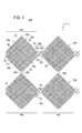
第1の実施の形態に係る導電シート(以下、第1導電シート10Aと記す)は、図1に示すように、第1透明基体12A(図2参照)の一主面上に、2以上の導電性の第1大格子14Aと、隣接する第1大格子14A間を電気的に接続する第1接続部16Aとが形成され、各第1大格子14Aは、それぞれ2以上の小格子18が組み合わされて構成され、第1接続部16Aは、小格子18のn倍(nは1より大きい実数)のピッチを有する1以上の中格子20(20a〜20d)が配置されて構成されている。小格子18は、ここでは一番小さい正方形状とされている。
As shown in FIG. 1, the conductive sheet according to the first embodiment (hereinafter referred to as the first
さらに、2以上の第1大格子14Aが第1接続部16Aを介してx方向(第1方向)に配列されて1つの第1透明導電パターン22Aが構成され、2以上の第1透明導電パターン22Aがx方向と直交するy方向(第2方向)に配列され、隣接する第1透明導電パターン22A間は電気的に絶縁された第1絶縁部24Aが配されている。
Further, two or more first
より具体的には、第1大格子14Aの4つの辺部のうち、隣接する第1大格子14Aと接続していない一方の頂点部分26aに隣接する第1辺部28a及び第2辺部28bについては、それぞれ第1辺部28a及び第2辺部28bに沿って連続する直線部30から多数の針状の線32(小格子18の辺)がくし歯状に張り出した形態とされている。一方、隣接する第1大格子14Aと接続していない他方の頂点部分26bに隣接する第3辺部28c及び第4辺部28dについては、それぞれ第3辺部28c及び第4辺部28dに沿って連続する直線部30が形成された形態とされ、さらに、他方の頂点部分26bに対応する1つの小格子18(正確には隣接する2つの辺)を取り外したような形態となっている。
More specifically, of the four side portions of the first
第1接続部16Aは、4つ分の小格子18を含む大きさを有する中格子20が4つ(第1中格子20a〜第4中格子20d)、ジグザグ状に配列された形状を有する。すなわち、第1中格子20aは、第2辺部28bの直線部30と第4辺部28dの直線部30との境界部分に存在し、1つの小格子18とL字状の空間が形成された形状を有する。第2中格子20bは、第1中格子20aの1つ辺(第2辺部28bの直線部30)に隣接し、正方形状の空間が形成された形状、すなわち、4つ分の小格子18をマトリクス状に配列し、中央の十字を取り外したような形状を有する。第3中格子20cは、第1中格子20aに隣接すると共に、第2中格子20bに隣接して配され、第2中格子20bと同様の形状を有する。第4中格子20dは、第3辺部28cの第2番目の直線部30(一番外側から第1大格子14Aの内方に向かって2番目の直線部30)と第1辺部28aとの境界部分に存在し、第2中格子20bに隣接すると共に、第3中格子20cに隣接して配され、第1中格子20aと同様に、1つの小格子18とL字状の空間が形成された形状を有する。第4中格子20dの1つの辺は第1大格子14Aにおける第4辺部28dの直線部30の延長上に存在する。そして、小格子18の配列ピッチをPsとしたとき、中格子20の配列ピッチPmは2×Psの関係を有している。
The first connecting
このように、第1導電シート10Aにおいては、1つの第1透明導電パターン22Aを、2以上の第1大格子14Aを第1接続部16Aを介してx方向に配列して構成し、各第1大格子14Aを、それぞれ2以上の小格子18を組み合わせて構成し、第1接続部16Aを、小格子18の2倍のピッチを有する4つの中格子20を配置して構成したので、1つの電極を1つのITO膜にて形成する構成よりも大幅に電気抵抗を低減することが可能となる。従って、この第1導電シート10Aを用いて例えば投影型静電容量方式のタッチパネルに適用した場合に、応答速度を速めることができ、タッチパネルの大サイズ化を促進させることができる。
As described above, in the first
次に、上述の第1導電シート10Aを用いたタッチパネル用の1組の導電シート、すなわち、第1の実施の形態に係るタッチパネル用導電シート(以下、第1タッチパネル用導電シート50Aと記す)について図3〜図6を参照しながら説明する。
この第1タッチパネル用導電シート50Aは、図3及び図4Aに示すように、上述した第1導電シート10Aと後述する第2導電シート10Bとが積層されて構成されている。
Next, a set of conductive sheets for a touch panel using the first
As shown in FIGS. 3 and 4A, the first touch panel
第1導電シート10Aは、上述したので、ここではその重複説明を省略するが、図3に示すように、各第1透明導電パターン22Aの一方の端部側に存在する第1大格子14Aの開放端は、第1接続部16Aが存在しない形状となっている。各第1透明導電パターン22Aの他方の端部側に存在する第1大格子14Aの端部は、第1外部配線40Aに電気的に接続されている。
Since the first
一方、第2導電シート10Bは、図3及び図4Aに示すように、第2透明基体12Bの一主面上に、2以上の導電性の第2大格子14Bと、隣接する第2大格子14B間を電気的に接続する第2接続部16Bとが形成され、各第2大格子14Bは、図5に示すように、それぞれ2以上の小格子18が組み合わされて構成され、第2接続部16Bは、小格子18のn倍(nは1より大きい実数)のピッチを有する1以上の中格子20が配置されて構成されている。
On the other hand, as shown in FIGS. 3 and 4A, the second
さらに、2以上の第2大格子14Bが第2接続部16Bを介してy方向(第2方向)に配列されて1つの第2透明導電パターン22Bが構成され、2以上の第2透明導電パターン22Bがy方向と直交するx方向(第1方向)に配列され、隣接する第2透明導電パターン22B間は電気的に絶縁された第2絶縁部24Bが配されている。
Further, two or more second
より具体的には、第2大格子14Bの4つの辺部のうち、隣接する第2大格子14Bと接続していない一方の頂点部分26aに隣接する第5辺部28e及び第6辺部28fについてみると、第5辺部28eについては、第1導電シート10Aにおける第1大格子14Aの第1辺部28aと同様に、第5辺部28eに沿って連続する直線部30から多数の針状の線32(小格子18の辺)がくし歯状に張り出した形態とされている。第6辺部28fについては、第1導電シート10Aにおける第1大格子14Aの第3辺部28cと同様に、第6辺部28fに沿って連続する直線部30が形成された形態とされている。隣接する第2大格子14Bと接続していない他方の頂点部分26bに隣接する第7辺部28g及び第8辺部28hについてみると、第7辺部26gについては、第5辺部28eと同様に、第7辺部28gに沿って連続する直線部30から多数の針状の線32(小格子18の辺)がくし歯状に張り出した形態とされ、第8辺部28hについては、第6辺部28fと同様に、第8辺部28hに沿って連続する直線部30が形成された形態とされている。
More specifically, among the four sides of the second
また、第2接続部16Bは、4つ分の小格子18を含む大きさを有する中格子20が4つ(第5中格子20e〜第8中格子20h)、ジグザグ状に配列された形状を有する。すなわち、第5中格子20eは、第6辺部28fの第2番目の直線部30(一番外側から第2大格子14Bの内方に向かって2番目の直線部)と第8辺部28hの直線部30との境界部分に存在し、1つの小格子18とL字状の空間が形成された形状を有する。第6中格子20fは、第5中格子20eの1つの辺(第6辺部28fの第2番目の直線部30)に隣接し、正方形状の空間が形成された形状、すなわち、4つ分の小格子18をマトリクス状に配列し、中央の十字を取り外したような形状を有する。第7中格子20gは、第5中格子20eに隣接すると共に、第6中格子20fに隣接して配され、第6中格子20fと同様の形状を有する。第8中格子20hは、第7辺部28gの直線部30と第5辺部28eとの境界部分に存在し、第6中格子20fに隣接すると共に、第7中格子20gに隣接して配され、第5中格子20eと同様に、1つの小格子18とL字状の空間が形成された形状を有する。第8中格子20hの1つの辺は第5中格子20eにおける第8辺部28hの直線部30の延長上に存在する。この第2導電シート10Bにおいても、小格子18の配列ピッチをPsとしたとき、中格子20の配列ピッチPmは2×Psの関係を有している。
The second connecting
図3に示すように、各第2透明導電パターン22Bの一方の端部側に存在する第2大格子14Bの開放端は、第2接続部16Bが存在しない形状となっている。各第2透明導電パターン22Bの他方の端部側に存在する第2大格子14Bの端部は、第2外部配線40Bに電気的に接続されている。
As shown in FIG. 3, the open end of the second
そして、例えば第2導電シート10B上に第1導電シート10Aを積層して第1タッチパネル用導電シート50Aとしたとき、図6に示すように、第1透明導電パターン22Aの第1接続部16Aと第2透明導電パターン22Bの第2接続部16Bとが第1透明基体12A(図4A参照)を間に挟んで対向し、第1透明導電パターン22Aの第1絶縁部24Aと第2透明導電パターン22Bの第2絶縁部24Bとが同じく第1透明基体12Aを間に挟んで対向した形態となる。なお、第1透明導電パターン22Aと第2透明導電パターン22Bの各線幅は同じであるが、図6においては、第1透明導電パターン22Aと第2透明導電パターン22Bの位置がわかるように、第1透明導電パターン22Aの線幅を太く、第2透明導電パターン22Bの線幅を細くして誇張して図示してある。
For example, when the first
積層した第1導電シート10A及び第2導電シート10Bを上面から見たとき、第1導電シート10Aに形成された第1大格子14Aの隙間を埋めるように、第2導電シート10Bの第2大格子14Bが配列された形態となる。つまり、大格子が敷き詰められた形態となる。このとき、第1大格子14Aの第1辺部28a及び第2辺部28bにおけるくし歯32の各先端が第2大格子14Bの第6辺部28f及び第8辺部28hの各直線部30にて接続されたような形状となって、結果的に小格子18が配列された形態となり、同様に、第2大格子14Bの第5辺部28e及び第7辺部28gにおけるくし歯32の各先端が第1大格子14Aの第3辺部28c及び第4辺部28dの各直線部30にて接続されたような形状となって、結果的に小格子18が配列された形態となり、第1大格子14Aと第2大格子14Bとの境界をほとんど見分けることができない状態となる。
When the stacked first
ここで、例えば第1大格子14A及び第2大格子14Bの辺部を全て直線部30として形成した場合、重ね合わせの位置精度の僅かなズレにより、直線部30同士の重なり部分の幅が大きくなり(線太り)、これにより、第1大格子14Aと第2大格子14Bとの境界が目立ってしまい、視認性が劣化するという問題が生じるが、本実施の形態では、上述したように、くし歯32の先端と直線部30との重なりにより、第1大格子14Aと第2大格子14Bとの境界が目立たなくなり、視認性が向上する。なお、第1絶縁部24Aと第2絶縁部24Bとが対向する部分は、中格子1つ分の開口が形成されることになるが、上述した線太りと異なり、光を遮るということがないため、外部に目立つということがほとんどない。特に、中格子1つ分の開口であれば、周りの小格子18と比してサイズ的にもほとんど同じであるため、さらに目立たなくなる。
Here, for example, when the side portions of the first
また、第1接続部16Aと第2接続部16Bとが対向した部分を上面から見たとき、第2接続部16Bの第5中格子20eと第7中格子20gとの交点が第1大格子14Aの第2中格子20bのほぼ中心に位置し、第2接続部16Bの第6中格子20fと第8中格子20hとの交点が第1大格子14Aの第3中格子20cのほぼ中心に位置することとなり、これら第1中格子20a〜第8中格子20hの組み合わせによって、複数の小格子18が形成された形態となる。すなわち、第1接続部16Aと第2接続部16Bとが対向した部分に、第1接続部16Aと第2接続部16Bの組み合わせによって、複数の小格子18が配列された形態となり、周りの第1大格子14Aを構成する小格子18や第2大格子14Bを構成する小格子18と見分けがつかなくなり、視認性が向上する。
Further, when the portion where the
そして、この第1タッチパネル用導電シート50Aをタッチパネルとして使用する場合は、第1導電シート10A上に保護層を形成し、第1導電シート10Aの多数の第1透明導電パターン22Aから導出された第1外部配線40Aと、第2導電シート10Bの多数の第2透明導電パターン22Bから導出された第2外部配線40Bとを、例えば位置演算を行うIC回路に接続する。
When this first touch panel
指先を保護層上に接触させることで、指先に対向する第1透明導電パターン22Aと第2透明導電パターン22Bからの信号がIC回路に伝達される。IC回路では、供給された信号に基づいて指先の位置を演算する。従って、同時に2つの指先を接触させても、各指先の位置を検出することが可能となる。
By bringing the fingertip into contact with the protective layer, signals from the first transparent
このように、第1タッチパネル用導電シート50Aにおいては、該第1タッチパネル用導電シート50Aを用いて例えば投影型静電容量方式のタッチパネルに適用した場合に、応答速度を速めることができ、タッチパネルの大サイズ化を促進させることができる。しかも、第1導電シート10Aの第1大格子14Aと第2導電シート10Bの第2大格子14Bとの境界が目立たなくなり、また、第1接続部16Aと第2接続部16Bとの組み合わせによって複数の小格子18が形づくられることから、局部的に線太りが生じる等の不都合がなくなり、全体として、視認性が良好となる。
As described above, in the first touch panel
上述の第1タッチパネル用導電シート50Aでは、図3及び図4Aに示すように、第1透明基体12Aの一主面に第1透明導電パターン22Aを形成し、第2透明基体12Bの一主面に第2透明導電パターン22Bを形成するようにしたが、その他、図4Bに示すように、第1透明基体12Aの一主面に第1透明導電パターン22Aを形成し、第1透明基体12Aの他主面に第2透明導電パターン22Bを形成するようにしてもよい。また、第1導電シート10Aと第2導電シート10Bとはその間に他の層が存在してもよく、第1透明導電パターン22Aと第2透明導電パターン22Bとが絶縁状態であれば、それらが対向して配置されてもよい。
In the first touch panel
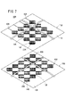
次に、第2の実施の形態に係るタッチパネル用導電シート(以下、第2タッチパネル用導電シート50Bと記す)について図7〜図10を参照しながら説明する。
この第2タッチパネル用導電シート50Bは、図7に示すように、上述した第1タッチパネル用導電シート50Aとほぼ同様の構成を有するが、図8に示すように、第1大格子14Aの第1辺部28a〜第4辺部28dがそれぞれ2以上の矩形形状が配列された矩形波形状を有し、図9に示すように、第2大格子14Bの第5辺部28e〜第8辺部28hがそれぞれ2以上の矩形形状が配列された矩形波形状を有する点で異なる。
Next, a touch panel conductive sheet (hereinafter referred to as a second touch panel
The second touch panel
具体的には、第1大格子14Aについては、図1に示す第1導電シート10Aの第1大格子14Aの第1辺部28a及び第2辺部28bの各くし歯32をそれぞれ1つ置きに繋いで、小格子18を1つ置きに配列させた形態にし、第3辺部28c及び第4辺部28dの各直線部30をそれぞれ1つ置きに分離して、小格子18を1つ置きに配列させた形態にすることで、図8に示すように、第2タッチパネル用導電シート50Bの第1大格子14Aの第1辺部28a〜第4辺部28dを、それぞれ2以上の矩形形状が配列された矩形波形状を有するようにし、特に、第1大格子14Aの第1辺部28aと該第1辺部28aと対向する第4辺部28dの各矩形波形状が互い違いとなり、第1大格子14Aの第2辺部28bと該第2辺部28bと対向する第3辺部28cの各矩形波形状が互い違いとなるようにしている。
Specifically, for the first
同様に、第2大格子14Bについて、図5に示す第2導電シート10B(第1タッチパネル用導電シート50A)の第2大格子14Bの第5辺部28e及び第7辺部28gの各くし歯32をそれぞれ1つ置きに繋いで、小格子18を1つ置きに配列させた形態にし、第6辺部26f及び第8辺部28hの各直線部30をそれぞれ1つ置きに分離して、小格子18を1つ置きに配列させた形態にすることで、第2タッチパネル用導電シート50Bの第2大格子14Bの第5辺部28e〜第8辺部28hを、それぞれ2以上の矩形形状が配列された矩形波形状を有するようにし、特に、第2大格子14Bの第5辺部28eと該
第5辺部28eと対向する第8辺部28hの各矩形波形状が互い違いとなり、第2大格子14Bの第6辺部28fと該第6辺部28fと対向する第7辺部28gの各矩形波形状が互い違いとなるようにしている。
Similarly, for the second
そして、例えば第2導電シート10B上に第1導電シート10Aを積層して第2タッチパネル用導電シート50Bとしたとき、図10に示すように、第1タッチパネル用導電シート50A(図6参照)の場合と同様に、第1透明導電パターン22Aの第1接続部16Aと第2透明導電パターン22Bの第2接続部16Bとが第1透明基体12A(図4A参照)を間に挟んで対向し、第1透明導電パターン22Aの第1絶縁部24Aと第2透明導電パターン22Bの第2絶縁部24Bとが第1透明基体12Aを間に挟んで対向した形態となる。なお、第1透明導電パターン22Aと第2透明導電パターン22Bの各線幅は同じであるが、図10においても図6と同様に、第1透明導電パターン22Aと第2透明導電パターン22Bの位置がわかるように、第1透明導電パターン22Aの線幅を太く、第2透明導電パターン22Bの線幅を細くして誇張して図示してある。
For example, when the first
積層した第1導電シート10A及び第2導電シート10Bを上面から見たとき、第1導電シート10Aに形成された第1大格子14Aの隙間を埋めるように、第2導電シート10Bの第2大格子14Bが配列された形態となる。このとき、第1大格子14Aの第1辺部28a及び第2辺部28bにおける各矩形波形状の凹部42aの開口部分が第2大格子14Bの第6辺部28f及び第8辺部28hの各矩形波形状の凸部18bの先端部分にて接続されたような形状となって、結果的に小格子18が連続して配列された形態となり、同様に、第1大格子14Aの第3辺部28c及び第4辺部28dにおける各矩形波形状の凹部42aの開口部分が第2大格子14Bの第5辺部28e及び第7辺部28gの各矩形波形状の凸部42bの先端部分にて接続されたような形状となって、結果的に小格子が連続して配列された形態となり、第1大格子14Aと第2大格子14Bとの境界をほとんど見分けることができない状態となる。つまり、矩形波形状の凹部42aの開口部分と凸部42bの先端部分との重なりにより、第1大格子14Aと第2大格子14Bとの境界が目立たなくなり、視認性が向上する。なお、第1絶縁部24Aと第2絶縁部24Bとが対向する部分は、十字形状の開口が形成されることになるが、上述した線太りと異なり、光を遮るということがないため、外部に目立つということがほとんどない。
When the stacked first
第1接続部16Aと第2接続部16Bとが対向した部分についても、第1タッチパネル用導電シート50Aと同様に、第2接続部16Bの第5中格子20eと第7中格子20gとの交点が第1接続部16Aの第2中格子20bのほぼ中心に位置し、第2接続部16Bの第6中格子20fと第8中格子20hとの交点が第1接続部16Aの第3中格子20cのほぼ中心に位置することとなり、これら第1中格子20a〜第8中格子20hの組み合わせによって、複数の小格子18が形成された形態となる。すなわち、第1接続部16Aと第2接続部16Bとが対向した部分に、第1接続部16Aと第2接続部16Bの組み合わせによって、複数の小格子18が配列された形態となり、周りの第1大格子14Aを構成する小格子18や第2大格子14Bを構成する小格子18と見分けがつかなくなり、視認性が向上する。
Also about the part where 16 A of 1st connection parts and the
このように、第2タッチパネル用導電シート50Bにおいても、該第2タッチパネル用導電シート50Bを用いて例えば投影型静電容量方式のタッチパネルに適用した場合に、応答速度を速めることができ、タッチパネルの大サイズ化を促進させることができる。しかも、第1導電シート10Aの第1大格子14Aと第2導電シート10Bの第2大格子14Bとの境界が目立たなくなり、また、第1接続部16Aと第2接続部16Bとの組み合わせによって複数の小格子18が形づくられることから、局部的に線太りが生じる等の不都合がなくなり、全体として、視認性が良好となる。
As described above, in the second touch panel
特に、この第2タッチパネル用導電シート50Bにおいては、第1大格子14Aの4つの辺(第1辺部28a〜第4辺部28d)並びに第2大格子14Bの4つの辺(第5辺部28e〜第8辺部28h)の形状がいずれも矩形波形状であって、各辺の形状が等価的に同一となっていることから、第1大格子14Aや第2大格子14Bの端部での電荷の局在化が抑制され、指先位置の誤検出を防ぐことができる。
In particular, in this second touch panel
上述した第1導電シート10A及び第2導電シート10Bにおいては、第1接続部16A及び第2接続部16Bを構成する中格子20の配列ピッチPmを小格子18の配列ピッチPsの2倍に設定したが、その他、1.5倍、3倍等、中格子の数に応じて任意に設定することができる。中格子20の配列ピッチPmは、その間隔が狭すぎたり、大きすぎたりすると、大格子14の配置が難しくなり、見栄えが悪くなることがあることから、小格子18の配列ピッチPsの1〜10倍が好ましく、1〜5倍がより好ましい。
In the first
また、小格子18のサイズ(1辺の長さや対角線の長さ等)や、第1大格子14Aを構成する小格子18の個数、第2大格子14Bを構成する小格子18の個数も、適用されるタッチパネルのサイズや分解能(配線数)に応じて適宜設定することができる。
Further, the size of the small lattice 18 (the length of one side, the length of the diagonal line, etc.), the number of
次に、第1導電シート10Aや第2導電シート10Bを製造する方法としては、例えば第1透明基体12A上及び第2透明基体12B上に感光性ハロゲン化銀塩を含有する乳剤層を有する感光材料を露光し、現像処理を施すことによって、露光部及び未露光部にそれぞれ金属銀部及び光透過性部を形成して第1透明導電パターン22A及び第2透明導電パターン22Bを形成するようにしてもよい。なお、さらに金属銀部に物理現像及び/又はめっき処理を施すことによって金属銀部に導電性金属を担持させるようにしてもよい。
Next, as a method for producing the first
あるいは、第1透明基体12A及び第2透明基体12B上に形成された銅箔上のフォトレジスト膜を露光、現像処理してレジストパターンを形成し、レジストパターンから露出する銅箔をエッチングすることによって、第1透明導電パターン22A及び第2透明導電パターン22Bを形成するようにしてもよい。
Alternatively, the photoresist film on the copper foil formed on the first
あるいは、第1透明基体12A及び第2透明基体12B上に金属微粒子を含むペーストを印刷し、ペーストに金属めっきを行うことによって、第1透明導電パターン22A及び第2透明導電パターン22Bを形成するようにしてもよい。
Alternatively, the first transparent
第1透明基体12A及び第2透明基体12B上に、第1透明導電パターン22A及び第2透明導電パターン22Bをスクリーン印刷版又はグラビア印刷版によって印刷形成するようにしてもよい。
The first transparent
次に、本実施の形態に係る第1導電シート10A及び第2導電シート10Bにおいて、特に好ましい態様であるハロゲン化銀写真感光材料を用いる方法を中心にして述べる。
本実施の形態に係る第1導電シート10A及び第2導電シート10Bの製造方法は、感光材料と現像処理の形態によって、次の3通りの形態が含まれる。
(1) 物理現像核を含まない感光性ハロゲン化銀黒白感光材料を化学現像又は熱現像して金属銀部を該感光材料上に形成させる態様。
(2) 物理現像核をハロゲン化銀乳剤層中に含む感光性ハロゲン化銀黒白感光材料を溶解物理現像して金属銀部を該感光材料上に形成させる態様。
(3) 物理現像核を含まない感光性ハロゲン化銀黒白感光材料と、物理現像核を含む非感光性層を有する受像シートを重ね合わせて拡散転写現像して金属銀部を非感光性受像シート上に形成させる態様。
Next, in the first
The manufacturing method of the first
(1) A mode in which a photosensitive silver halide black-and-white photosensitive material not containing physical development nuclei is chemically developed or thermally developed to form a metallic silver portion on the photosensitive material.
(2) An embodiment in which a photosensitive silver halide black-and-white photosensitive material containing physical development nuclei in a silver halide emulsion layer is dissolved and physically developed to form a metallic silver portion on the photosensitive material.
(3) A photosensitive silver halide black-and-white photosensitive material containing no physical development nuclei and an image receiving sheet having a non-photosensitive layer containing physical development nuclei are overlapped and developed by diffusion transfer, and the metallic silver portion is non-photosensitive image-receiving sheet. Form formed on top.
上記(1)の態様は、一体型黒白現像タイプであり、感光材料上に光透過性導電膜等の透光性導電性膜が形成される。得られる現像銀は化学現像銀又は熱現像銀であり、高比表面のフィラメントである点で後続するめっき又は物理現像過程で活性が高い。
上記(2)の態様は、露光部では、物理現像核近縁のハロゲン化銀粒子が溶解されて現像核上に沈積することによって感光材料上に光透過性導電性膜等の透光性導電性膜が形成される。これも一体型黒白現像タイプである。現像作用が、物理現像核上への析出であるので高活性であるが、現像銀は比表面の小さい球形である。
上記(3)の態様は、未露光部においてハロゲン化銀粒子が溶解されて拡散して受像シート上の現像核上に沈積することによって受像シート上に光透過性導電性膜等の透光性導電性膜が形成される。いわゆるセパレートタイプであって、受像シートを感光材料から剥離して用いる態様である。
The aspect (1) is an integrated black-and-white development type, and a light-transmitting conductive film such as a light-transmitting conductive film is formed on the photosensitive material. The resulting developed silver is chemically developed silver or heat developed silver, and is highly active in the subsequent plating or physical development process in that it is a filament with a high specific surface.
In the above aspect (2), the light-transmitting conductive film such as a light-transmitting conductive film is formed on the photosensitive material by dissolving silver halide grains close to the physical development nucleus and depositing on the development nucleus in the exposed portion. A characteristic film is formed. This is also an integrated black-and-white development type. Although the development action is precipitation on the physical development nuclei, it is highly active, but developed silver is a sphere with a small specific surface.
In the above aspect (3), the silver halide grains are dissolved and diffused in the unexposed area and deposited on the development nuclei on the image receiving sheet, whereby a light transmitting conductive film or the like is formed on the image receiving sheet. A conductive film is formed. This is a so-called separate type in which the image receiving sheet is peeled off from the photosensitive material.
いずれの態様もネガ型現像処理及び反転現像処理のいずれの現像を選択することもできる(拡散転写方式の場合は、感光材料としてオートポジ型感光材料を用いることによってネガ型現像処理が可能となる)。 In either embodiment, either negative development processing or reversal development processing can be selected (in the case of the diffusion transfer method, negative development processing is possible by using an auto-positive type photosensitive material as the photosensitive material). .
ここでいう化学現像、熱現像、溶解物理現像、拡散転写現像は、当業界で通常用いられている用語どおりの意味であり、写真化学の一般教科書、例えば菊地真一著「写真化学」(共立出版社、1955年刊行)、C.E.K.Mees編「The Theory of Photographic Processes, 4th ed.」(Mcmillan社、1977年刊行)に解説されている。本件は液処理に係る発明であるが、その他の現像方式として熱現像方式を適用する技術も参考にすることができる。例えば、特開2004−184693号、同2004−334077号、同2005−010752号の各公報、特願2004−244080号、同2004−085655号の各明細書に記載された技術を適用することができる。 The chemical development, thermal development, dissolution physical development, and diffusion transfer development mentioned here have the same meanings as are commonly used in the industry, and are general textbooks of photographic chemistry such as Shinichi Kikuchi, “Photochemistry” (Kyoritsu Publishing) (Published in 1955), C.I. E. K. It is described in "The Theory of Photographic Processes, 4th ed." Edited by Mees (Mcmillan, 1977). Although this case is an invention related to liquid processing, a technique of applying a thermal development system as another development system can also be referred to. For example, the techniques described in Japanese Patent Application Laid-Open Nos. 2004-184893, 2004-334077, and 2005-010752, and Japanese Patent Application Nos. 2004-244080 and 2004-085655 can be applied. it can.
ここで、本実施の形態に係る第1導電シート10A及び第2導電シート10Bの各層の構成について、以下に詳細に説明する。
Here, the configuration of each layer of the first
[第1透明基体12A、第2透明基体12B]
第1透明基体12A及び第2透明基体12Bとしては、プラスチックフイルム、プラスチック板、ガラス板等を挙げることができる。
[First
Examples of the first
上記プラスチックフイルム及びプラスチック板の原料としては、例えば、ポリエチレンテレフタレート(PET)、ポリエチレンナフタレート(PEN)等のポリエステル類;ポリエチレン(PE)、ポリプロピレン(PP)、ポリスチレン、EVA等のポリオレフィン類;ビニル系樹脂;その他、ポリカーボネート(PC)、ポリアミド、ポリイミド、アクリル樹脂、トリアセチルセルロース(TAC)等を用いることができる。 Examples of the raw material for the plastic film and the plastic plate include polyesters such as polyethylene terephthalate (PET) and polyethylene naphthalate (PEN); polyolefins such as polyethylene (PE), polypropylene (PP), polystyrene, and EVA; Resin; In addition, polycarbonate (PC), polyamide, polyimide, acrylic resin, triacetyl cellulose (TAC) and the like can be used.
第1透明基体12A及び第2透明基体12Bとしては、PET(融点:258℃)、PEN(融点:269℃)、PE(融点:135℃)、PP(融点:163℃)、ポリスチレン(融点:230℃)、ポリ塩化ビニル(融点:180℃)、ポリ塩化ビニリデン(融点:212℃)やTAC(融点:290℃)等の融点が約290℃以下であるプラスチックフィルム、又はプラスチック板が好ましく、特に、光透過性や加工性等の観点から、PETが好ましい。第1タッチパネル用導電シート50Aや第2タッチパネル用導電シート50Bに使用される第1導電シート10A及び第2導電シート10Bのような透明導電性フイルムは透明性が要求されるため、第1透明基体12A及び第2透明基体12Bの透明度は高いことが好ましい。
As the first
[銀塩乳剤層]
第1導電シート10A及び第2導電シート10Bの導電層(第1大格子14A、第1接続部16A、第2大格子14B、第2接続部16B、小格子18等の導電部)となる銀塩乳剤層は、銀塩とバインダーの他、溶媒や染料等の添加剤を含有する。
[Silver salt emulsion layer]
Silver used as conductive layers (conductive portions such as the first
本実施の形態に用いられる銀塩としては、ハロゲン化銀等の無機銀塩及び酢酸銀等の有機銀塩が挙げられる。本実施の形態においては、光センサーとしての特性に優れるハロゲン化銀を用いることが好ましい。 Examples of the silver salt used in the present embodiment include inorganic silver salts such as silver halide and organic silver salts such as silver acetate. In the present embodiment, it is preferable to use silver halide having excellent characteristics as an optical sensor.
銀塩乳剤層の塗布銀量(銀塩の塗布量)は、銀に換算して1〜30g/m2が好ましく、1〜25g/m2がより好ましく、5〜20g/m2がさらに好ましい。この塗布銀量を上記範囲とすることで、第1タッチパネル用導電シート50Aや第2タッチパネル用導電シート50Bとした場合に所望の表面抵抗を得ることができる。
Silver coating amount of silver salt emulsion layer (coating amount of silver salt) is preferably from 1 to 30 g / m 2 in terms of silver, more preferably 1 to 25 g / m 2, more preferably 5 to 20 g / m 2 . By setting the coated silver amount within the above range, a desired surface resistance can be obtained when the first touch panel
本実施の形態に用いられるバインダーとしては、例えば、ゼラチン、ポリビニルアルコール(PVA)、ポリビニルピロリドン(PVP)、澱粉等の多糖類、セルロース及びその誘導体、ポリエチレンオキサイド、ポリビニルアミン、キトサン、ポリリジン、ポリアクリル酸、ポリアルギン酸、ポリヒアルロン酸、カルボキシセルロース等が挙げられる。これらは、官能基のイオン性によって中性、陰イオン性、陽イオン性の性質を有する。 Examples of the binder used in the present embodiment include gelatin, polyvinyl alcohol (PVA), polyvinyl pyrrolidone (PVP), starch and other polysaccharides, cellulose and derivatives thereof, polyethylene oxide, polyvinyl amine, chitosan, polylysine, and polyacryl. Examples include acid, polyalginic acid, polyhyaluronic acid, carboxycellulose and the like. These have neutral, anionic, and cationic properties depending on the ionicity of the functional group.
本実施の形態の銀塩乳剤層16中に含有されるバインダーの含有量は、特に限定されず、分散性と密着性を発揮し得る範囲で適宜決定することができる。銀塩乳剤層16中のバインダーの含有量は、銀/バインダー体積比で1/4以上が好ましく、1/2以上がより好ましい。銀/バインダー体積比は、100/1以下が好ましく、50/1以下がより好ましい。また、銀/バインダー体積比は1/1〜4/1であることがさらに好ましい。1/1〜3/1であることが最も好ましい。銀塩乳剤層中の銀/バインダー体積比をこの範囲にすることで、塗布銀量を調整した場合でも抵抗値のばらつきを抑制し、均一な表面抵抗を有する第1タッチパネル用導電シート50Aや第2タッチパネル用導電シート50Bを得ることができる。なお、銀/バインダー体積比は、原料のハロゲン化銀量/バインダー量(重量比)を銀量/バインダー量(重量比)に変換し、さらに、銀量/バインダー量(重量比)を銀量/バインダー量(体積比)に変換することで求めることができる。
The content of the binder contained in the silver salt emulsion layer 16 of the present embodiment is not particularly limited, and can be appropriately determined as long as dispersibility and adhesion can be exhibited. The content of the binder in the silver salt emulsion layer 16 is preferably 1/4 or more, and more preferably 1/2 or more in terms of a silver / binder volume ratio. The silver / binder volume ratio is preferably 100/1 or less, and more preferably 50/1 or less. The silver / binder volume ratio is more preferably 1/1 to 4/1. Most preferably, it is 1/1 to 3/1. By setting the silver / binder volume ratio in the silver salt emulsion layer within this range, even when the amount of coated silver is adjusted, variation in resistance value is suppressed, and the first touch panel
<溶媒>
銀塩乳剤層の形成に用いられる溶媒は、特に限定されるものではないが、例えば、水、有機溶媒(例えば、メタノール等のアルコール類、アセトン等のケトン類、ホルムアミド等のアミド類、ジメチルスルホキシド等のスルホキシド類、酢酸エチル等のエステル類、エーテル類等)、イオン性液体、及びこれらの混合溶媒を挙げることができる。
本実施の形態の銀塩乳剤層に用いられる溶媒の含有量は、銀塩乳剤層に含まれる銀塩、バインダー等の合計の質量に対して30〜90質量%の範囲であり、50〜80質量%の範囲であることが好ましい。
<その他の添加剤>
本実施の形態に用いられる各種添加剤に関しては、特に制限は無く、公知のものを好ましく用いることができる。
<Solvent>
The solvent used for forming the silver salt emulsion layer is not particularly limited. For example, water, organic solvents (for example, alcohols such as methanol, ketones such as acetone, amides such as formamide, dimethyl sulfoxide, etc. Sulphoxides such as, esters such as ethyl acetate, ethers, etc.), ionic liquids, and mixed solvents thereof.
The content of the solvent used in the silver salt emulsion layer of the present embodiment is in the range of 30 to 90% by mass with respect to the total mass of the silver salt and binder contained in the silver salt emulsion layer, and 50 to 80 It is preferably in the range of mass%.
<Other additives>
There are no particular restrictions on the various additives used in the present embodiment, and known ones can be preferably used.
[その他の層構成]
銀塩乳剤層の上に図示しない保護層を設けてもよい。本実施の形態において「保護層」とは、ゼラチンや高分子ポリマーといったバインダーからなる層を意味し、擦り傷防止や力学特性を改良する効果を発現するために感光性を有する銀塩乳剤層上に形成される。その厚みは0.5μm以下が好ましい。保護層の塗布方法及び形成方法は特に限定されず、公知の塗布方法及び形成方法を適宜選択することができる。また、銀塩乳剤層16よりも下に、例えば下塗り層を設けることもできる。
[Other layer structure]
A protective layer (not shown) may be provided on the silver salt emulsion layer. In the present embodiment, the “protective layer” means a layer made of a binder such as gelatin or a high molecular polymer, and is formed on a silver salt emulsion layer having photosensitivity in order to exhibit an effect of preventing scratches and improving mechanical properties. It is formed. The thickness is preferably 0.5 μm or less. The coating method and forming method of the protective layer are not particularly limited, and a known coating method and forming method can be appropriately selected. An undercoat layer, for example, can be provided below the silver salt emulsion layer 16.
次に、第1導電シート10A及び第2導電シート10Bの作製方法の各工程について説明する。
Next, each step of the manufacturing method of the first
[露光]
本実施の形態では、第1透明導電パターン22A及び第2透明導電パターン22Bを印刷方式によって施す場合を含むが、印刷方式以外は、第1透明導電パターン22A及び第2透明導電パターン22Bを露光と現像等によって形成する。すなわち、第1透明基体12A及び第2透明基体12B上に設けられた銀塩含有層を有する感光材料又はフォトリソグラフィ用フォトポリマーを塗工した感光材料への露光を行う。露光は、電磁波を用いて行うことができる。電磁波としては、例えば、可視光線、紫外線等の光、X線等の放射線等が挙げられる。さらに露光には波長分布を有する光源を利用してもよく、特定の波長の光源を用いてもよい。
[exposure]
The present embodiment includes the case where the first transparent
[現像処理]
本実施の形態では、乳剤層を露光した後、さらに現像処理が行われる。現像処理は、銀塩写真フイルムや印画紙、印刷製版用フイルム、フォトマスク用エマルジョンマスク等に用いられる通常の現像処理の技術を用いることができる。現像液については特に限定はしないが、PQ現像液、MQ現像液、MAA現像液等を用いることもでき、市販品では、例えば、富士フイルム社処方のCN−16、CR−56、CP45X、FD−3、パピトール、KODAK社処方のC−41、E−6、RA−4、D−19、D−72等の現像液、又はそのキットに含まれる現像液を用いることができる。また、リス現像液を用いることもできる。
[Development processing]
In this embodiment, after the emulsion layer is exposed, development processing is further performed. The development processing can be performed by a normal development processing technique used for silver salt photographic film, photographic paper, printing plate-making film, photomask emulsion mask, and the like. The developer is not particularly limited, but PQ developer, MQ developer, MAA developer and the like can also be used, and commercially available products include, for example, CN-16, CR-56, CP45X, FD prescribed by Fuji Film -3, Papitol, a developer such as C-41, E-6, RA-4, D-19, D-72, etc. formulated by KODAK, or a developer included in the kit can be used. A lith developer can also be used.
本発明における現像処理は、未露光部分の銀塩を除去して安定化させる目的で行われる定着処理を含むことができる。本発明における定着処理は、銀塩写真フイルムや印画紙、印刷製版用フイルム、フォトマスク用エマルジョンマスク等に用いられる定着処理の技術を用いることができる。 The development processing in the present invention can include a fixing processing performed for the purpose of removing and stabilizing the silver salt in the unexposed portion. For the fixing process in the present invention, a fixing process technique used for silver salt photographic film, photographic paper, film for printing plate making, emulsion mask for photomask, and the like can be used.
上記定着工程における定着温度は、約20℃〜約50℃が好ましく、さらに好ましくは25〜45℃である。また、定着時間は5秒〜1分が好ましく、さらに好ましくは7秒〜50秒である。定着液の補充量は、感光材料の処理量に対して600ml/m2以下が好ましく、500ml/m2以下がさらに好ましく、300ml/m2以下が特に好ましい。 The fixing temperature in the fixing step is preferably about 20 ° C. to about 50 ° C., more preferably 25 to 45 ° C. The fixing time is preferably 5 seconds to 1 minute, more preferably 7 seconds to 50 seconds. The replenishing amount of the fixing solution is preferably 600 ml / m 2 or less with respect to the processing of the photosensitive material, more preferably 500 ml / m 2 or less, 300 ml / m 2 or less is particularly preferred.
現像、定着処理を施した感光材料は、水洗処理や安定化処理を施されるのが好ましい。上記水洗処理又は安定化処理においては、水洗水量は通常感光材料1m2当り、20リットル以下で行われ、3リットル以下の補充量(0も含む、すなわちため水水洗)で行うこともできる。 The light-sensitive material that has been subjected to development and fixing processing is preferably subjected to water washing treatment or stabilization treatment. In the water washing treatment or the stabilization treatment, the washing water amount is usually 20 liters or less per 1 m 2 of the light-sensitive material, and can be replenished in 3 liters or less (including 0, ie, rinsing with water).
現像処理後の露光部に含まれる金属銀の質量は、露光前の露光部に含まれていた銀の質量に対して50質量%以上の含有率であることが好ましく、80質量%以上であることがさらに好ましい。露光部に含まれる銀の質量が露光前の露光部に含まれていた銀の質量に対して50質量%以上であれば、高い導電性を得ることができるため好ましい。 The mass of the metallic silver contained in the exposed portion after the development treatment is preferably a content of 50% by mass or more, and 80% by mass or more with respect to the mass of silver contained in the exposed portion before exposure. More preferably. If the mass of silver contained in the exposed portion is 50% by mass or more based on the mass of silver contained in the exposed portion before exposure, it is preferable because high conductivity can be obtained.
本実施の形態における現像処理後の階調は、特に限定されるものではないが、4.0を超えることが好ましい。現像処理後の階調が4.0を超えると、光透過性部の透光性を高く保ったまま、導電性金属部の導電性を高めることができる。階調を4.0以上にする手段としては、例えば、前述のロジウムイオン、イリジウムイオンのドープが挙げられる。 The gradation after the development processing in the present embodiment is not particularly limited, but is preferably more than 4.0. When the gradation after the development processing exceeds 4.0, the conductivity of the conductive metal portion can be increased while keeping the light transmissive property of the light transmissive portion high. Examples of means for setting the gradation to 4.0 or higher include the aforementioned doping of rhodium ions and iridium ions.
以上の工程を経て導電シートは得られるが、得られた導電シートの表面抵抗は0.1〜100オーム/sq.の範囲にあることが好ましく、1〜10オーム/sq.の範囲にあることがより好ましい。また、現像処理後の導電シートに対しては、さらにカレンダー処理を行ってもよく、カレンダー処理により所望の表面抵抗に調整することができる。 Although the conductive sheet is obtained through the above steps, the surface resistance of the obtained conductive sheet is 0.1 to 100 ohm / sq. Is preferably in the range of 1 to 10 ohm / sq. It is more preferable that it is in the range. Further, the conductive sheet after the development treatment may be further subjected to a calendar treatment, and can be adjusted to a desired surface resistance by the calendar treatment.
[物理現像及びめっき処理]
本実施の形態では、前記露光及び現像処理により形成された金属銀部の導電性を向上させる目的で、前記金属銀部に導電性金属粒子を担持させるための物理現像及び/又はめっき処理を行ってもよい。本発明では物理現像又はめっき処理のいずれか一方のみで導電性金属粒子を金属性銀部に担持させてもよく、物理現像とめっき処理とを組み合わせて導電性金属粒子を金属銀部に担持させてもよい。なお、金属銀部に物理現像及び/又はめっき処理を施したものを含めて「導電性金属部」と称する。
[Physical development and plating]
In the present embodiment, for the purpose of improving the conductivity of the metallic silver portion formed by the exposure and development processing, physical development and / or plating treatment for supporting the conductive metal particles on the metallic silver portion is performed. May be. In the present invention, the conductive metal particles may be supported on the metallic silver portion by only one of physical development and plating treatment, or the conductive metal particles are supported on the metallic silver portion by combining physical development and plating treatment. May be. In addition, the thing which performed the physical development and / or the plating process to the metal silver part is called "conductive metal part".
本実施の形態における「物理現像」とは、金属や金属化合物の核上に、銀イオン等の金属イオンを還元剤で還元して金属粒子を析出させることをいう。この物理現象は、インスタントB&Wフイルム、インスタントスライドフイルムや、印刷版製造等に利用されており、本発明ではその技術を用いることができる。また、物理現像は、露光後の現像処理と同時に行っても、現像処理後に別途行ってもよい。 “Physical development” in the present embodiment means that metal particles such as silver ions are reduced by a reducing agent on metal or metal compound nuclei to deposit metal particles. This physical phenomenon is used for instant B & W film, instant slide film, printing plate manufacturing, and the like, and the technology can be used in the present invention. Further, the physical development may be performed simultaneously with the development processing after exposure or separately after the development processing.
本実施の形態において、めっき処理は、無電解めっき(化学還元めっきや置換めっき)、電解めっき、又は無電解めっきと電解めっきの両方を用いることができる。本実施の形態における無電解めっきは、公知の無電解めっき技術を用いることができ、例えば、プリント配線板等で用いられている無電解めっき技術を用いることができ、無電解めっきは無電解銅めっきであることが好ましい。 In the present embodiment, the plating treatment can use electroless plating (chemical reduction plating or displacement plating), electrolytic plating, or both electroless plating and electrolytic plating. For the electroless plating in the present embodiment, a known electroless plating technique can be used, for example, an electroless plating technique used in a printed wiring board or the like can be used. Plating is preferred.
[酸化処理]
本実施の形態では、現像処理後の金属銀部、並びに、物理現像及び/又はめっき処理によって形成された導電性金属部には、酸化処理を施すことが好ましい。酸化処理を行うことにより、例えば、光透過性部に金属が僅かに沈着していた場合に、該金属を除去し、光透過性部の透過性をほぼ100%にすることができる。
[Oxidation treatment]
In the present embodiment, it is preferable to subject the metallic silver portion after the development treatment and the conductive metal portion formed by physical development and / or plating treatment to oxidation treatment. By performing the oxidation treatment, for example, when a metal is slightly deposited on the light transmissive portion, the metal can be removed and the light transmissive portion can be made almost 100% transparent.
[導電性金属部]
本実施の形態の導電性金属部の線幅は、5μm以上200μm(0.2mm)以下から選択可能であるが、タッチパネルの材料としての用途である場合、5μm以上50μm以下が好ましい。さらに好ましくは5μm以上30μm以下、最も好ましくは5μm以上20μm以下である。線間隔は30μm以上500μm以下であることが好ましく、さらに好ましくは50μm以上400μm以下、最も好ましくは100μm以上350μm以下である。また、導電性金属部は、アース接続等の目的においては、線幅は200μmより広い部分を有していてもよい。
[Conductive metal part]
The line width of the conductive metal portion of the present embodiment can be selected from 5 μm to 200 μm (0.2 mm), but is preferably 5 μm to 50 μm when used as a touch panel material. More preferably, they are 5 micrometers or more and 30 micrometers or less, Most preferably, they are 5 micrometers or more and 20 micrometers or less. The line spacing is preferably 30 μm or more and 500 μm or less, more preferably 50 μm or more and 400 μm or less, and most preferably 100 μm or more and 350 μm or less. The conductive metal portion may have a portion whose line width is wider than 200 μm for the purpose of ground connection or the like.
本実施の形態における導電性金属部は、可視光透過率の点から開口率は85%以上であることが好ましく、90%以上であることがさらに好ましく、95%以上であることが最も好ましい。開口率とは、第1大格子14A、第1接続部16A、第2大格子14B、第2接続部16B、小格子18等の導電部を除いた透光性部分が全体に占める割合であり、例えば、線幅15μm、ピッチ300μmの正方形の格子状の開口率は、90%である。
The conductive metal portion in the present embodiment preferably has an aperture ratio of 85% or more, more preferably 90% or more, and most preferably 95% or more from the viewpoint of visible light transmittance. The aperture ratio is the ratio of the light-transmitting portions excluding the conductive portions such as the first
[光透過性部]
本実施の形態における「光透過性部」とは、第1導電シート10A及び第2導電シート10Bのうち導電性金属部以外の透光性を有する部分を意味する。光透過性部における透過率は、前述のとおり、第1透明基体12A及び第2透明基体12Bの光吸収及び反射の寄与を除いた380〜780nmの波長領域における透過率の最小値で示される透過率が90%以上、好ましくは95%以上、さらに好ましくは97%以上であり、さらにより好ましくは98%以上であり、最も好ましくは99%以上である。
[Light transmissive part]
The “light transmissive part” in the present embodiment means a part having translucency other than the conductive metal part in the first
露光方法に関しては、ガラスマスクを介した方法やレーザー描画によるパターン露光方式が好ましい。 Regarding the exposure method, a method through a glass mask or a pattern exposure method by laser drawing is preferable.
[第1導電シート10A及び第2導電シート10B]
本実施の形態に係る第1導電シート10A及び第2導電シート10Bにおける第1透明基体12A及び第2透明基体12Bの厚さは、5〜350μmであることが好ましく、30〜150μmであることがさらに好ましい。5〜350μmの範囲であれば所望の可視光の透過率が得られ、且つ、取り扱いも容易である。
[First
The thickness of the first
第1透明基体12A及び第2透明基体12B上に設けられる金属銀部の厚さは、第1透明基体12A及び第2透明基体12B上に塗布される銀塩含有層用塗料の塗布厚みに応じて適宜決定することができる。金属銀部の厚さは、0.001mm〜0.2mmから選択可能であるが、30μm以下であることが好ましく、20μm以下であることがより好ましく、0.01〜9μmであることがさらに好ましく、0.05〜5μmであることが最も好ましい。また、金属銀部はパターン状であることが好ましい。金属銀部は1層でもよく、2層以上の重層構成であってもよい。金属銀部がパターン状であり、且つ、2層以上の重層構成である場合、異なる波長に感光できるように、異なる感色性を付与することができる。これにより、露光波長を変えて露光すると、各層において異なるパターンを形成することができる。
The thickness of the metallic silver portion provided on the first
導電性金属部の厚さは、タッチパネルの用途としては、薄いほど表示パネルの視野角が広がるため好ましく、視認性の向上の点でも薄膜化が要求される。このような観点から、導電性金属部に担持された導電性金属からなる層の厚さは、9μm未満であることが好ましく、0.1μm以上5μm未満であることがより好ましく、0.1μm以上3μm未満であることがさらに好ましい。 As the thickness of the conductive metal part, the thinner the display panel, the wider the viewing angle of the display panel, and the thinner the display is required for improving the visibility. From such a viewpoint, the thickness of the layer made of the conductive metal carried on the conductive metal part is preferably less than 9 μm, more preferably 0.1 μm or more and less than 5 μm, and more preferably 0.1 μm or more. More preferably, it is less than 3 μm.
本実施の形態では、上述した銀塩含有層の塗布厚みをコントロールすることにより所望の厚さの金属銀部を形成し、さらに物理現像及び/又はめっき処理により導電性金属粒子からなる層の厚みを自在にコントロールできるため、5μm未満、好ましくは3μm未満の厚みを有する第1導電シート10A及び第2導電シート10Bであっても容易に形成することができる。
In the present embodiment, the thickness of the layer made of conductive metal particles is formed by controlling the coating thickness of the silver salt-containing layer described above to form a metallic silver portion having a desired thickness, and further by physical development and / or plating treatment. Therefore, even the first
なお、本実施の形態に係る第1導電シート10Aや第2導電シート10Bの製造方法では、めっき等の工程は必ずしも行う必要はない。本実施の形態に係る第1導電シート10Aや第2導電シート10Bの製造方法では銀塩乳剤層の塗布銀量、銀/バインダー体積比を調整することで所望の表面抵抗を得ることができるからである。なお、必要に応じてカレンダー処理等を行ってもよい。
In addition, in the manufacturing method of the first
(現像処理後の硬膜処理)
銀塩乳剤層に対して現像処理を行った後に、硬膜剤に浸漬して硬膜処理を行うことが好ましい。硬膜剤としては、例えば、グルタルアルデヒド、アジポアルデヒド、2,3−ジヒドロキシ−1,4−ジオキサン等のジアルデヒド類及びほう酸等の特開平2−141279号に記載のものを挙げることができる。
(Hardening after development)
It is preferable to perform a film hardening process by immersing the film in a hardener after the silver salt emulsion layer is developed. Examples of the hardener include dialdehydes such as glutaraldehyde, adipaldehyde, 2,3-dihydroxy-1,4-dioxane, and those described in JP-A-2-141279 such as boric acid. .
なお、本発明は、下記表1及び表2に記載の公開公報及び国際公開パンフレットの技術と適宜組合わせて使用することができる。「特開」、「号公報」、「号パンフレット」等の表記は省略する。 In addition, this invention can be used in combination with the technique of the publication gazette and international publication pamphlet which are described in following Table 1 and Table 2. FIG. Notations such as “JP,” “Gazette” and “No. Pamphlet” are omitted.

以下に、本発明の実施例を挙げて本発明をさらに具体的に説明する。なお、以下の実施例に示される材料、使用量、割合、処理内容、処理手順等は、本発明の趣旨を逸脱しない限り適宜変更することができる。従って、本発明の範囲は以下に示す具体例により限定的に解釈されるべきものではない。 Hereinafter, the present invention will be described more specifically with reference to examples of the present invention. In addition, the material, usage-amount, ratio, processing content, processing procedure, etc. which are shown in the following Examples can be changed suitably unless it deviates from the meaning of this invention. Accordingly, the scope of the present invention should not be construed as being limited by the specific examples shown below.
(ハロゲン化銀感光材料)
水媒体中のAg150gに対してゼラチン10.0gを含む、球相当径平均0.1μmの沃臭塩化銀粒子(I=0.2モル%、Br=40モル%)を含有する乳剤を調製した。
(Silver halide photosensitive material)
An emulsion containing 10.0 g of gelatin per 150 g of Ag in an aqueous medium and containing silver iodobromochloride grains having an average equivalent sphere diameter of 0.1 μm (I = 0.2 mol%, Br = 40 mol%) was prepared. .
また、この乳剤中にはK3Rh2Br9及びK2IrCl6を濃度が10−7(モル/モル銀)になるように添加し、臭化銀粒子にRhイオンとIrイオンをドープした。この乳剤にNa2PdCl4を添加し、さらに塩化金酸とチオ硫酸ナトリウムを用いて金硫黄増感を行った後、ゼラチン硬膜剤と共に、銀の塗布量が10g/m2となるように第1透明基体12A及び第2透明基体12B(ここでは、共にポリエチレンテレフタレート(PET))上に塗布した。この際、Ag/ゼラチン体積比は2/1とした。
In this emulsion, K 3 Rh 2 Br 9 and K 2 IrCl 6 were added so as to have a concentration of 10 −7 (mol / mol silver), and silver bromide grains were doped with Rh ions and Ir ions. . After adding Na 2 PdCl 4 to this emulsion and further performing gold-sulfur sensitization using chloroauric acid and sodium thiosulfate, together with the gelatin hardener, the coating amount of silver was 10 g / m 2. The coating was applied on the first
幅30cmのPET支持体に25cmの幅で20m分塗布を行ない、塗布の中央部24cmを残すように両端を3cmずつ切り落としてロール状のハロゲン化銀感光材料を得た。 Coating was performed for 20 m with a width of 25 cm on a PET support having a width of 30 cm, and both ends were cut off by 3 cm so as to leave a central portion of the coating, thereby obtaining a roll-shaped silver halide photosensitive material.
(露光)
露光のパターンは、第1タッチパネル用導電シート50Aの第1導電シート10Aについては図1及び図3に示すパターンで、第2導電シート10Bについては図3及び図5に示すパターンで、A4サイズ(210mm×297mm)の第1透明基体12A及び第2透明基体12Bに行った。第2タッチパネル用導電シート50Bの第1導電シート10Aについては図7及び図8に示すパターンで、第2導電シート10Bについては図7及び図9に示すパターンで、A4サイズ(210mm×297mm)の第1透明基体12A及び第2透明基体12Bに行った。小格子18の配列ピッチPsを200μmとし、中格子20の配列ピッチPmを2×Psとした。また、小格子18の導電部の厚みを2μmとし、幅を10μmとした。露光は上記パターンのフォトマスクを介して高圧水銀ランプを光源とした平行光を用いて露光した。
(exposure)
The pattern of exposure is the pattern shown in FIGS. 1 and 3 for the first
(現像処理)
・現像液1L処方
ハイドロキノン 20 g
亜硫酸ナトリウム 50 g
炭酸カリウム 40 g
エチレンジアミン・四酢酸 2 g
臭化カリウム 3 g
ポリエチレングリコール2000 1 g
水酸化カリウム 4 g
pH 10.3に調整
・定着液1L処方
チオ硫酸アンモニウム液(75%) 300 ml
亜硫酸アンモニウム・1水塩 25 g
1,3−ジアミノプロパン・四酢酸 8 g
酢酸 5 g
アンモニア水(27%) 1 g
pH 6.2に調整
上記処理剤を用いて露光済み感材を、富士フイルム社製自動現像機 FG−710PTSを用いて処理条件:現像35℃ 30秒、定着34℃ 23秒、水洗 流水(5L/分)の20秒処理で行った。
(Development processing)
・ Developer 1L formulation Hydroquinone 20 g
Sodium sulfite 50 g
Potassium carbonate 40 g
Ethylenediamine tetraacetic acid 2 g
Potassium bromide 3 g
Polyethylene glycol 2000 1 g
Potassium hydroxide 4 g
Adjusted to pH 10.3 and formulated 1L fixer ammonium thiosulfate solution (75%) 300 ml
Ammonium sulfite monohydrate 25 g
1,3-diaminopropane tetraacetic acid 8 g
Acetic acid 5 g
Ammonia water (27%) 1 g
Adjusted to pH 6.2 Processed photosensitive material using the above processing agent using Fujifilm's automatic processor FG-710PTS Processing conditions: development 35 ° C. for 30 seconds, fixing 34 ° C. for 23 seconds, washed water (5 L / Min) for 20 seconds.
〔評価〕
(表面抵抗測定)
表面抵抗率の均一性を評価するために、第1導電シート10A及び第2導電シート10Bの表面抵抗率をダイアインスツルメンツ社製ロレスターGP(型番MCP−T610)直列4探針プローブ(ASP)にて任意の10箇所測定した値の平均値である。
[Evaluation]
(Surface resistance measurement)
In order to evaluate the uniformity of the surface resistivity, the surface resistivity of the first
(視認性の評価)
第1導電シート10A及び第2導電シート10Bを貼り合わせて、第1タッチパネル用導電シート50A及び第2タッチパネル用導電シート50Bを作製し、肉眼で、線太りや黒い斑点がないかどうかを確認した。
(Visibility evaluation)
The first
(評価結果)
表面抵抗は、第1導電シート10A及び第2導電シート10B共に、5オーム/sq.であり、A4サイズの大きさを有する投影型静電容量方式のタッチパネルに十分に適用できることがわかった。また、第1タッチパネル用導電シート50A及び第2タッチパネル用導電シート50B共に、線太りや黒い斑点は確認されず、視認性は良好であった。
(Evaluation results)
The surface resistance is 5 ohm / sq. For both the first
なお、本発明に係る導電シート、導電シートの使用方法及びタッチパネルは、上述の実施の形態に限らず、本発明の要旨を逸脱することなく、種々の構成を採り得ることはもちろんである。 Note that the conductive sheet, the method of using the conductive sheet, and the touch panel according to the present invention are not limited to the above-described embodiments, and various configurations can be adopted without departing from the gist of the present invention.
10A…第1導電シート 10B…第2導電シート
12A…第1透明基体 12B…第2透明基体
14A…第1大格子 14B…第2大格子
16A…第1接続部 16B…第2接続部
18…小格子 20…中格子
20a〜20h…第1中格子〜第8中格子
22A…第1透明導電パターン 22B…第2透明導電パターン
24A…第1絶縁部 24B…第2絶縁部
28a〜28h…第1辺部〜第8辺部
50A…第1タッチパネル用導電シート
50B…第2タッチパネル用導電シート
DESCRIPTION OF
Claims (31)
各前記大格子は、それぞれ2以上の小格子が組み合わされて構成され、
前記接続部は、前記小格子のn倍(nは1より大きい実数)のピッチを有する複数の中格子がジグザグ状に配列された形状を有することを特徴とする導電シート。 On the substrate, two or more conductive large lattices and a connecting portion for electrically connecting the adjacent large lattices are formed,
Each of the large lattices is configured by combining two or more small lattices,
The connecting portion, the conductive sheet having a plurality of in lattice and wherein Rukoto which have a sequence shape in a zigzag shape having a pitch of n times the small lattices (n is a real number larger than 1).
各前記大格子は、それぞれ2以上の小格子が組み合わされて構成され、
前記接続部は、前記小格子のn倍(nは1より大きい実数)のピッチを有する複数の中格子を有し、
1つの前記小格子とL字状の空間が形成された第1中格子と、4つ分の前記小格子をマトリクス状に配列し、中央の十字を取り外した形状を有する第2中格子が直列に接続されて構成されていることを特徴とする導電シート。 On the substrate, two or more conductive large lattices and a connecting portion for electrically connecting the adjacent large lattices are formed,
Each of the large lattices is configured by combining two or more small lattices,
The connecting portion includes a plurality of medium lattices having a pitch n times (n is a real number greater than 1) the small lattice,
A first medium lattice in which one small lattice and an L-shaped space are formed, and a second medium lattice having a shape in which the four small lattices are arranged in a matrix and the central cross is removed are connected in series. An electrically conductive sheet characterized by being connected to .
各前記大格子は、それぞれ2以上の小格子が組み合わされて構成され、
前記接続部は、前記小格子のn倍(nは1より大きい実数)のピッチを有する1以上の中格子が配置されて構成され、
前記小格子を構成する導電性金属部の線幅が200μm以下、
前記導電性金属部の線間隔が30μm以上500μm以下、
前記導電性金属部の厚さが9μm未満、
前記基体の厚さが5〜350μmであることを特徴とする導電シート。 On the substrate, two or more conductive large lattices and a connecting portion for electrically connecting the adjacent large lattices are formed,
Each of the large lattices is configured by combining two or more small lattices,
The connecting portion is configured by arranging one or more medium lattices having a pitch n times (n is a real number larger than 1) the small lattice,
The line width of the conductive metal part constituting the small lattice is 200 μm or less,
The line spacing of the conductive metal part is 30 μm or more and 500 μm or less,
The conductive metal portion has a thickness of less than 9 μm;
Conductive sheet the thickness of the substrate, characterized in 5~350μm der Rukoto.
各前記大格子は、それぞれ2以上の小格子が組み合わされて構成され、
前記接続部は、前記小格子のn倍(nは1より大きい実数)のピッチを有する1以上の中格子が配置されて構成され、
前記小格子を構成する導電性金属部の線幅が200μm以下、
前記導電性金属部の厚さが9μm未満であることを特徴とする導電シート。 On the substrate, two or more conductive large lattices and a connecting portion for electrically connecting the adjacent large lattices are formed,
Each of the large lattices is configured by combining two or more small lattices,
The connecting portion is configured by arranging one or more medium lattices having a pitch n times (n is a real number larger than 1) the small lattice,
The line width of the conductive metal part constituting the small lattice is 200 μm or less,
Conductive sheet thickness of the conductive metal portion, characterized in der Rukoto less than 9 .mu.m.
前記接続部は、複数の前記中格子がジグザグ状に配列された形状を有することを特徴とする導電シート。 In the electrically conductive sheet of any one of Claims 2-4 ,
The connecting portion has a shape in which a plurality of the intermediate grids are arranged in a zigzag shape.
前記接続部は、1つの前記小格子とL字状の空間が形成された第1中格子と、4つ分の前記小格子をマトリクス状に配列し、中央の十字を取り外した形状を有する第2中格子が直列に接続されて構成されていることを特徴とする導電シート。 In the conductive sheet according to claim 3 or 4 ,
The connecting portion has a shape in which one small lattice and a first middle lattice in which an L-shaped space is formed, and the four small lattices are arranged in a matrix, and a central cross is removed. 2. A conductive sheet comprising a grid of 2 connected in series.
前記接続部は、1つの前記小格子とL字状の空間が形成された複数の前記中格子を有することを特徴とする導電シート。 In the conductive sheet according to any one of claims 1 to 6 ,
The connection portion includes a plurality of the intermediate lattices in which one small lattice and an L-shaped space are formed.
前記中格子の配列ピッチは、前記小格子の配列ピッチの1〜10倍であることを特徴とする導電シート。 In the conductive sheet according to any one of claims 1 to 7 ,
The conductive sheet is characterized in that the arrangement pitch of the medium lattice is 1 to 10 times the arrangement pitch of the small lattice.
前記小格子の配列ピッチをPs、前記中格子の配列ピッチをPmとしたとき、
Pm=2×Ps
を満足することを特徴とする導電シート。 In the electrically conductive sheet of any one of Claims 1-8 ,
When the arrangement pitch of the small lattices is Ps and the arrangement pitch of the medium lattices is Pm,
Pm = 2 × Ps
A conductive sheet characterized by satisfying
2以上の前記大格子が前記接続部を介して一方向に配列されていることを特徴とする導電シート。 In the electrically conductive sheet of any one of Claims 1-9 ,
A conductive sheet, wherein two or more of the large lattices are arranged in one direction through the connecting portion.
2以上の前記大格子が前記接続部を介して第1方向に配列されて1つの透明導電パターンが構成され、
2以上の前記透明導電パターンが前記第1方向と直交する第2方向に配列され、
隣接する前記透明導電パターン間は電気的に絶縁された絶縁部が配されていることを特徴とする導電シート。 In the conductive sheet according to any one of claims 1 to 10 ,
Two or more of the large lattices are arranged in the first direction through the connection portion to constitute one transparent conductive pattern,
Two or more transparent conductive patterns are arranged in a second direction orthogonal to the first direction;
An electrically conductive sheet, wherein an electrically insulated insulating portion is disposed between the adjacent transparent conductive patterns.
前記基体の他方の主面に、2以上の導電性の第2大格子と、隣接する前記第2大格子間を電気的に接続する第2接続部とが形成され、
各前記第1大格子及び各前記第2大格子は、それぞれ2以上の小格子が組み合わされて構成され、
前記第1接続部及び前記第2接続部は、それぞれ前記小格子のn倍(nは1より大きい実数)のピッチを有する1以上の中格子が配置されて構成され、
2以上の前記第1大格子が前記第1接続部を介して第1方向に配列されて1つの第1透明導電パターンが構成され、
2以上の前記第2大格子が前記第2接続部を介して前記第1方向と直交する第2方向に配列されて1つの第2透明導電パターンが構成され、
2以上の前記第1透明導電パターンが前記第2方向に配列され、
2以上の前記第2透明導電パターンが前記第1方向に配列され、
隣接する前記第1透明導電パターン間は電気的に絶縁された第1絶縁部が配され、
隣接する前記第2透明導電パターン間は電気的に絶縁された第2絶縁部が配され、
前記第1接続部と前記第2接続部とが前記基体を間に挟んで対向し、
前記第1絶縁部と前記第2絶縁部とが前記基体を間に挟んで対向しており、
前記第1絶縁部と前記第2絶縁部とが前記基体を間に挟んで対向する部分は、前記小格子が2以上配列された大きさの開口が形成された形態を有することを特徴とする導電シート。 One main surface of the base is formed with two or more conductive first large lattices and a first connection portion that electrically connects the adjacent first large lattices,
Two or more conductive second large lattices and a second connection portion for electrically connecting the adjacent second large lattices are formed on the other main surface of the base body,
Each of the first large lattice and each of the second large lattices is configured by combining two or more small lattices,
Each of the first connection part and the second connection part is configured by arranging one or more medium lattices each having a pitch n times (n is a real number larger than 1) the small lattice ,
Two or more of the first large lattices are arranged in the first direction via the first connection portion to constitute one first transparent conductive pattern,
Two or more second large lattices are arranged in a second direction orthogonal to the first direction via the second connection portion to constitute one second transparent conductive pattern,
Two or more first transparent conductive patterns are arranged in the second direction;
Two or more second transparent conductive patterns are arranged in the first direction;
A first insulating portion that is electrically insulated is disposed between the adjacent first transparent conductive patterns,
A second insulating portion that is electrically insulated is disposed between the adjacent second transparent conductive patterns,
The first connection portion and the second connection portion are opposed to each other with the base interposed therebetween,
The first insulating portion and the second insulating portion are opposed to each other with the base interposed therebetween,
Wherein the first insulating portion of the second insulating portion is opposed to each other between said substrates, characterized Rukoto to have a form in which opening of the small lattices two or more sequences magnitude is formed A conductive sheet.
前記部分は、前記中格子1つ分の大きさの開口が形成された形態を有することを特徴とする導電シート。 The conductive sheet according to claim 12 ,
The conductive sheet is characterized in that the portion has a form in which an opening having a size corresponding to the one of the middle grids is formed.
前記部分は、複数の前記小格子がほぼ十字形状に配列された大きさの開口が形成された形態を有する導電シート。 The conductive sheet according to claim 12 or 13 ,
The portion is a conductive sheet having a form in which an opening having a size in which a plurality of the small lattices are arranged in a substantially cross shape is formed.
前記基体の他方の主面に、2以上の導電性の第2大格子と、隣接する前記第2大格子間を電気的に接続する第2接続部とが形成され、
各前記第1大格子及び各前記第2大格子は、それぞれ2以上の小格子が組み合わされて構成され、
前記第1接続部及び前記第2接続部は、それぞれ前記小格子のn倍(nは1より大きい実数)のピッチを有する1以上の中格子が配置されて構成され、
前記第1大格子のうち、第1の辺は、該第1の辺に沿って連続する直線部から多数の針状の線がくし歯状に張り出した形態を有し、前記第1の辺と対向する第2の辺は、該第2の辺に沿って連続する直線部が形成された形態を有し、
前記第2大格子のうち、前記基体を介して前記第1大格子の前記第1の辺と対向する第3の辺は、該第3の辺に沿って連続する直線部が形成された形態を有し、前記基体を介して前記第1大格子の前記第2の辺と対向する第4の辺は、該第1の辺に沿って連続する直線部から多数の針状の線がくし歯状に張り出した形態を有することを特徴とする導電シート。 One main surface of the base is formed with two or more conductive first large lattices and a first connection portion that electrically connects the adjacent first large lattices,
Two or more conductive second large lattices and a second connection portion for electrically connecting the adjacent second large lattices are formed on the other main surface of the base body,
Each of the first large lattice and each of the second large lattices is configured by combining two or more small lattices,
Each of the first connection part and the second connection part is configured by arranging one or more medium lattices each having a pitch n times (n is a real number larger than 1) the small lattice,
Of the first large lattice, the first side has a form in which a large number of needle-like lines project in a comb-tooth shape from a linear portion continuous along the first side, and the first side and The opposing second side has a form in which a straight line portion continuous along the second side is formed,
Of the second large lattice, a third side facing the first side of the first large lattice through the base is formed with a linear portion continuous along the third side. And the fourth side facing the second side of the first large lattice via the base body has a plurality of needle-like lines combed from a straight line portion continuous along the first side. A conductive sheet characterized by having a shape protruding in a shape.
前記基体の他方の主面に、2以上の導電性の第2大格子と、隣接する前記第2大格子間を電気的に接続する第2接続部とが形成され、
各前記第1大格子及び各前記第2大格子は、それぞれ2以上の小格子が組み合わされて構成され、
前記第1接続部及び前記第2接続部は、それぞれ前記小格子のn倍(nは1より大きい実数)のピッチを有する1以上の中格子が配置されて構成され、
前記小格子を構成する導電性金属部の線幅が200μm以下、
前記導電性金属部の線間隔が30μm以上500μm以下、
前記導電性金属部の厚さが9μm未満、
前記基体の厚さが5〜350μmであることを特徴とする導電シート。 One main surface of the base is formed with two or more conductive first large lattices and a first connection portion that electrically connects the adjacent first large lattices,
Two or more conductive second large lattices and a second connection portion for electrically connecting the adjacent second large lattices are formed on the other main surface of the base body,
Each of the first large lattice and each of the second large lattices is configured by combining two or more small lattices,
Each of the first connection part and the second connection part is configured by arranging one or more medium lattices each having a pitch n times (n is a real number larger than 1) the small lattice,
The line width of the conductive metal part constituting the small lattice is 200 μm or less,
The line spacing of the conductive metal part is 30 μm or more and 500 μm or less,
The conductive metal portion has a thickness of less than 9 μm;
A conductive sheet having a thickness of the substrate of 5 to 350 μm .
前記基体の他方の主面に、2以上の導電性の第2大格子と、隣接する前記第2大格子間を電気的に接続する第2接続部とが形成され、Two or more conductive second large lattices and a second connection portion for electrically connecting the adjacent second large lattices are formed on the other main surface of the base body,
各前記第1大格子及び各前記第2大格子は、それぞれ2以上の小格子が組み合わされて構成され、Each of the first large lattice and each of the second large lattices is configured by combining two or more small lattices,
前記第1接続部及び前記第2接続部は、それぞれ前記小格子のn倍(nは1より大きい実数)のピッチを有する1以上の中格子が配置されて構成され、Each of the first connection part and the second connection part is configured by arranging one or more medium lattices each having a pitch n times (n is a real number larger than 1) the small lattice,
前記小格子を構成する導電性金属部の線幅が200μm以下、The line width of the conductive metal part constituting the small lattice is 200 μm or less,
前記導電性金属部の厚さが9μm未満であることを特徴とする導電シート。A conductive sheet, wherein the conductive metal portion has a thickness of less than 9 μm.
2以上の前記第1大格子が前記第1接続部を介して第1方向に配列されて1つの第1透明導電パターンが構成され、
2以上の前記第2大格子が前記第2接続部を介して前記第1方向と直交する第2方向に配列されて1つの第2透明導電パターンが構成され、
2以上の前記第1透明導電パターンが前記第2方向に配列され、
2以上の前記第2透明導電パターンが前記第1方向に配列され、
隣接する前記第1透明導電パターン間は電気的に絶縁された第1絶縁部が配され、
隣接する前記第2透明導電パターン間は電気的に絶縁された第2絶縁部が配され、
前記第1接続部と前記第2接続部とが前記基体を間に挟んで対向し、
前記第1絶縁部と前記第2絶縁部とが前記基体を間に挟んで対向していることを特徴とする導電シート。 The conductive sheet according to any one of claims 15 to 17 ,
Two or more of the first large lattices are arranged in the first direction via the first connection portion to constitute one first transparent conductive pattern,
Two or more second large lattices are arranged in a second direction orthogonal to the first direction via the second connection portion to constitute one second transparent conductive pattern,
Two or more first transparent conductive patterns are arranged in the second direction;
Two or more second transparent conductive patterns are arranged in the first direction;
A first insulating portion that is electrically insulated is disposed between the adjacent first transparent conductive patterns,
A second insulating portion that is electrically insulated is disposed between the adjacent second transparent conductive patterns,
The first connection portion and the second connection portion are opposed to each other with the base interposed therebetween,
The conductive sheet, wherein the first insulating portion and the second insulating portion are opposed to each other with the base interposed therebetween.
前記第1大格子のうち、第1の辺は、該第1の辺に沿って連続する直線部から多数の針状の線がくし歯状に張り出した形態を有し、前記第1の辺と対向する第2の辺は、該第2の辺に沿って連続する直線部が形成された形態を有し、
前記第2大格子のうち、前記基体を介して前記第1大格子の前記第1の辺と対向する第3の辺は、該第3の辺に沿って連続する直線部が形成された形態を有し、前記基体を介して前記第1大格子の前記第2の辺と対向する第4の辺は、該第1の辺に沿って連続する直線部から多数の針状の線がくし歯状に張り出した形態を有することを特徴とする導電シート。 In the electrically conductive sheet according to any one of claims 12 to 14, 16, and 17 ,
Of the first large lattice, the first side has a form in which a large number of needle-like lines project in a comb-tooth shape from a linear portion continuous along the first side, and the first side and The opposing second side has a form in which a straight line portion continuous along the second side is formed,
Of the second large lattice, a third side facing the first side of the first large lattice through the base is formed with a linear portion continuous along the third side. And the fourth side facing the second side of the first large lattice via the base body has a plurality of needle-like lines combed from a straight line portion continuous along the first side. A conductive sheet characterized by having a shape protruding in a shape.
前記小格子を構成する導電性金属部の線幅が200μm以下、
前記導電性金属部の線間隔が30μm以上500μm以下、
前記導電性金属部の厚さが9μm未満、
前記基体の厚さが5〜350μmであることを特徴とする導電シート。 The conductive sheet according to any one of claims 12 to 14 ,
The line width of the conductive metal part constituting the small lattice is 200 μm or less,
The line spacing of the conductive metal part is 30 μm or more and 500 μm or less,
The conductive metal portion has a thickness of less than 9 μm;
A conductive sheet having a thickness of the substrate of 5 to 350 μm.
前記小格子は正方形状であることを特徴とする導電シート。 In the conductive sheet according to any one of claims 12 to 20 ,
The conductive sheet is characterized in that the small lattice has a square shape.
前記第1接続部及び第2接続部は、複数の前記中格子がジグザグ状に配列された形状を有することを特徴とする導電シート。The conductive sheet, wherein the first connection part and the second connection part have a shape in which a plurality of the intermediate grids are arranged in a zigzag shape.
前記第1接続部及び前記第2接続部は、1つの前記小格子とL字状の空間が形成された複数の前記中格子を有することを特徴とする導電シート。The said 1st connection part and the said 2nd connection part have the said some lattice and the said some grid | lattice in which L-shaped space was formed, The electrically conductive sheet characterized by the above-mentioned.
前記中格子の配列ピッチは、前記小格子の配列ピッチの1〜10倍であることを特徴とする導電シート。The conductive sheet is characterized in that the arrangement pitch of the medium lattice is 1 to 10 times the arrangement pitch of the small lattice.
前記小格子の配列ピッチをPs、前記中格子の配列ピッチをPmとしたとき、When the arrangement pitch of the small lattices is Ps and the arrangement pitch of the medium lattices is Pm,
Pm=2×PsPm = 2 × Ps
を満足することを特徴とする導電シート。A conductive sheet characterized by satisfying
2以上の導電性の第2大格子と、隣接する前記第2大格子間を電気的に接続する第2接続部とが形成され、各前記第2大格子は、それぞれ2以上の小格子が組み合わされて構成され、前記第2接続部は、それぞれ前記小格子のn倍(nは1より大きい実数)のピッチを有する1以上の中格子が配置されて構成された第2導電シートとを使用する導電シートの使用方法であって、
前記第1導電シートは、2以上の前記第1大格子が前記第1接続部を介して第1方向に配列されて1つの第1透明導電パターンが構成され、
前記第2導電シートは、2以上の前記第2大格子が前記第2接続部を介して前記第1方向と直交する第2方向に配列されて1つの第2透明導電パターンが構成され、
前記小格子を構成する導電性金属部の線幅が200μm以下、
前記導電性金属部の線間隔が30μm以上500μm以下、
前記導電性金属部の厚さが9μm未満、
前記基体の厚さが5〜350μmであり、
前記第1導電シートと前記第2導電シートとを組み合わせることで、前記第1導電シートの前記第1接続部と前記第2導電シートの前記第2接続部とが組み合わさって前記小格子の配列を形成するように配置して使用することを特徴とする導電シートの使用方法。 Two or more conductive first large lattices and a first connection portion for electrically connecting the adjacent first large lattices are formed, and each of the first large lattices has two or more small lattices. A first conductive sheet configured by combining one or more medium lattices each having a pitch of n times (n is a real number larger than 1) each of the small lattices.
Two or more conductive second large lattices and a second connection portion for electrically connecting the adjacent second large lattices are formed, and each of the second large lattices has two or more small lattices. A second conductive sheet configured by arranging one or more medium lattices each having a pitch of n times (n is a real number larger than 1) each of the small lattices. A method of using a conductive sheet to be used,
In the first conductive sheet, two or more first large lattices are arranged in the first direction via the first connection portion to constitute one first transparent conductive pattern,
In the second conductive sheet, two or more second large lattices are arranged in a second direction orthogonal to the first direction via the second connection portion to constitute one second transparent conductive pattern,
The line width of the conductive metal part constituting the small lattice is 200 μm or less,
The line spacing of the conductive metal part is 30 μm or more and 500 μm or less,
The conductive metal portion has a thickness of less than 9 μm;
The substrate has a thickness of 5 to 350 μm;
By combining the first conductive sheet and the second conductive sheet, the first connection portion of the first conductive sheet and the second connection portion of the second conductive sheet are combined to form the arrangement of the small lattices. using conductive sheet, characterized in that arranged and used to form the.
2以上の導電性の第2大格子と、隣接する前記第2大格子間を電気的に接続する第2接続部とが形成され、各前記第2大格子は、それぞれ2以上の小格子が組み合わされて構成され、前記第2接続部は、それぞれ前記小格子のn倍(nは1より大きい実数)のピッチを有する1以上の中格子が配置されて構成された第2導電シートとを使用する導電シートの使用方法であって、Two or more conductive second large lattices and a second connection portion for electrically connecting the adjacent second large lattices are formed, and each of the second large lattices has two or more small lattices. A second conductive sheet configured by arranging one or more medium lattices each having a pitch of n times (n is a real number larger than 1) each of the small lattices. A method of using a conductive sheet to be used,
前記第1導電シートは、2以上の前記第1大格子が前記第1接続部を介して第1方向に配列されて1つの第1透明導電パターンが構成され、In the first conductive sheet, two or more first large lattices are arranged in the first direction via the first connection portion to constitute one first transparent conductive pattern,
前記第2導電シートは、2以上の前記第2大格子が前記第2接続部を介して前記第1方向と直交する第2方向に配列されて1つの第2透明導電パターンが構成され、In the second conductive sheet, two or more second large lattices are arranged in a second direction orthogonal to the first direction via the second connection portion to constitute one second transparent conductive pattern,
前記小格子を構成する導電性金属部の線幅が200μm以下、The line width of the conductive metal part constituting the small lattice is 200 μm or less,
前記導電性金属部の厚さが9μm未満であり、The conductive metal portion has a thickness of less than 9 μm;
前記第1導電シートと前記第2導電シートとを組み合わせることで、前記第1導電シートの前記第1接続部と前記第2導電シートの前記第2接続部とが組み合わさって前記小格子の配列を形成するように配置して使用することを特徴とする導電シートの使用方法。By combining the first conductive sheet and the second conductive sheet, the first connection portion of the first conductive sheet and the second connection portion of the second conductive sheet are combined to form the arrangement of the small lattices. A method of using a conductive sheet, wherein the conductive sheet is used so as to form a film.
前記第1接続部及び第2接続部は、複数の前記中格子がジグザグ状に配列された形状を有することを特徴とする導電シートの使用方法。The method for using a conductive sheet, wherein the first connection portion and the second connection portion have a shape in which a plurality of the intermediate lattices are arranged in a zigzag shape.
前記中格子の配列ピッチは、前記小格子の配列ピッチの1〜10倍であることを特徴とする導電シートの使用方法。The method for using a conductive sheet, wherein the arrangement pitch of the medium lattice is 1 to 10 times the arrangement pitch of the small lattice.
前記小格子の配列ピッチをPs、前記中格子の配列ピッチをPmとしたとき、When the arrangement pitch of the small lattices is Ps and the arrangement pitch of the medium lattices is Pm,
Pm=2×PsPm = 2 × Ps
を満足することを特徴とする導電シートの使用方法。A method of using a conductive sheet characterized by satisfying
Priority Applications (1)
| Application Number | Priority Date | Filing Date | Title |
|---|---|---|---|
| JP2010120331A JP4820451B2 (en) | 2009-11-20 | 2010-05-26 | Conductive sheet, method of using conductive sheet, and touch panel |
Applications Claiming Priority (3)
| Application Number | Priority Date | Filing Date | Title |
|---|---|---|---|
| JP2009265467 | 2009-11-20 | ||
| JP2009265467 | 2009-11-20 | ||
| JP2010120331A JP4820451B2 (en) | 2009-11-20 | 2010-05-26 | Conductive sheet, method of using conductive sheet, and touch panel |
Publications (2)
| Publication Number | Publication Date |
|---|---|
| JP2011129501A JP2011129501A (en) | 2011-06-30 |
| JP4820451B2 true JP4820451B2 (en) | 2011-11-24 |
Family
ID=44291580
Family Applications (2)
| Application Number | Title | Priority Date | Filing Date |
|---|---|---|---|
| JP2010120331A Active JP4820451B2 (en) | 2009-11-20 | 2010-05-26 | Conductive sheet, method of using conductive sheet, and touch panel |
| JP2010258859A Active JP5629194B2 (en) | 2009-11-20 | 2010-11-19 | Conductive sheet, method of using conductive sheet, and capacitive touch panel |
Family Applications After (1)
| Application Number | Title | Priority Date | Filing Date |
|---|---|---|---|
| JP2010258859A Active JP5629194B2 (en) | 2009-11-20 | 2010-11-19 | Conductive sheet, method of using conductive sheet, and capacitive touch panel |
Country Status (1)
| Country | Link |
|---|---|
| JP (2) | JP4820451B2 (en) |
Cited By (2)
| Publication number | Priority date | Publication date | Assignee | Title |
|---|---|---|---|---|
| US10228782B2 (en) | 2013-03-04 | 2019-03-12 | Fujifilm Corporation | Transparent conductive film and touch panel |
| US10317598B2 (en) | 2013-06-26 | 2019-06-11 | Fujifilm Corporation | Optical film, polarization plate, transparent conductive film, surface protection film, and liquid crystal display apparatus having negative birefringence |
Families Citing this family (25)
| Publication number | Priority date | Publication date | Assignee | Title |
|---|---|---|---|---|
| JP5661533B2 (en) * | 2010-05-28 | 2015-01-28 | 富士フイルム株式会社 | Manufacturing method of conductive sheet and manufacturing method of touch panel |
| JP5808966B2 (en) | 2011-07-11 | 2015-11-10 | 富士フイルム株式会社 | Conductive laminate, touch panel and display device |
| JP5785040B2 (en) * | 2011-09-06 | 2015-09-24 | 富士フイルム株式会社 | Manufacturing method and program for conductive sheet |
| WO2013008826A1 (en) | 2011-07-11 | 2013-01-17 | 富士フイルム株式会社 | Conductive sheet, touch panel, display device, method for producing said conductive sheet, and recording medium |
| JP5806559B2 (en) * | 2011-09-06 | 2015-11-10 | 富士フイルム株式会社 | Conductive sheet, touch panel and display device |
| CN102902425B (en) * | 2011-07-28 | 2016-06-08 | 宸鸿科技(厦门)有限公司 | Capacitance type touch-control panel structure and manufacture method |
| KR101587486B1 (en) | 2011-07-29 | 2016-01-21 | 미쓰비시 세이시 가부시키가이샤 | Translucent electrode |
| DE102011108803B4 (en) * | 2011-07-29 | 2017-06-29 | Polyic Gmbh & Co. Kg | A plastic film touch sensor, use of the plastic film and method of making a multimodal input device |
| CN102981664B (en) | 2011-09-07 | 2016-10-05 | 宸鸿科技(厦门)有限公司 | Touch electrode structure and the contact panel of application thereof |
| KR101645828B1 (en) | 2011-12-16 | 2016-08-04 | 후지필름 가부시키가이샤 | Electroconductive sheet and touch panel |
| JP5875484B2 (en) | 2011-12-22 | 2016-03-02 | 富士フイルム株式会社 | Conductive sheet and touch panel |
| JP2013149232A (en) | 2011-12-22 | 2013-08-01 | Fujifilm Corp | Conductive sheet and touch panel |
| JP5822395B2 (en) * | 2012-01-25 | 2015-11-24 | 富士フイルム株式会社 | Conductive sheet, inspection method and manufacturing method thereof |
| WO2013140859A1 (en) | 2012-03-22 | 2013-09-26 | シャープ株式会社 | Electrode sheet, touch panel, and display apparatus |
| JP2013225296A (en) * | 2012-03-23 | 2013-10-31 | Fujifilm Corp | Conductive member, touch panel using the same, display device, and input device |
| WO2013157526A1 (en) | 2012-04-16 | 2013-10-24 | シャープ株式会社 | Touch panel substrate and display apparatus |
| KR101521681B1 (en) * | 2012-04-24 | 2015-05-19 | 삼성전기주식회사 | Touch Panel |
| JP5849059B2 (en) * | 2012-07-06 | 2016-01-27 | 富士フイルム株式会社 | Conductive film for touch panel and touch panel |
| US9459744B2 (en) | 2012-07-31 | 2016-10-04 | Sharp Kabushiki Kaisha | Touch panel substrate and display device |
| JP6129611B2 (en) * | 2013-03-27 | 2017-05-17 | 大日本印刷株式会社 | Manufacturing method of touch panel |
| CN105009044B (en) * | 2013-03-29 | 2017-08-08 | 夏普株式会社 | Touch panel substrate and electronic equipment |
| JP5969961B2 (en) | 2013-07-12 | 2016-08-17 | 富士フイルム株式会社 | Wiring board |
| WO2015045603A1 (en) * | 2013-09-25 | 2015-04-02 | シャープ株式会社 | Conductive sheet, touch panel device, display device, and method for manufacturing conductive sheet |
| JP6348874B2 (en) | 2015-05-19 | 2018-06-27 | 富士フイルム株式会社 | Touch sensor panel |
| JP6421077B2 (en) | 2015-05-19 | 2018-11-07 | 富士フイルム株式会社 | Antenna manufacturing method and touch sensor |
Family Cites Families (3)
| Publication number | Priority date | Publication date | Assignee | Title |
|---|---|---|---|---|
| TW200901014A (en) * | 2007-06-28 | 2009-01-01 | Sense Pad Tech Co Ltd | Touch panel device |
| JP5174575B2 (en) * | 2008-07-31 | 2013-04-03 | グンゼ株式会社 | Touch panel |
| JP5361579B2 (en) * | 2009-07-09 | 2013-12-04 | 信越ポリマー株式会社 | Sensor panel for large display and manufacturing method thereof |
-
2010
- 2010-05-26 JP JP2010120331A patent/JP4820451B2/en active Active
- 2010-11-19 JP JP2010258859A patent/JP5629194B2/en active Active
Cited By (3)
| Publication number | Priority date | Publication date | Assignee | Title |
|---|---|---|---|---|
| US10228782B2 (en) | 2013-03-04 | 2019-03-12 | Fujifilm Corporation | Transparent conductive film and touch panel |
| US10684710B2 (en) | 2013-03-04 | 2020-06-16 | Fujifilm Corporation | Transparent conductive film and touch panel |
| US10317598B2 (en) | 2013-06-26 | 2019-06-11 | Fujifilm Corporation | Optical film, polarization plate, transparent conductive film, surface protection film, and liquid crystal display apparatus having negative birefringence |
Also Published As
| Publication number | Publication date |
|---|---|
| JP5629194B2 (en) | 2014-11-19 |
| JP2011129112A (en) | 2011-06-30 |
| JP2011129501A (en) | 2011-06-30 |
Similar Documents
| Publication | Publication Date | Title |
|---|---|---|
| JP4820451B2 (en) | Conductive sheet, method of using conductive sheet, and touch panel | |
| JP5676225B2 (en) | Conductive sheet, method of using conductive sheet, and capacitive touch panel | |
| TWI494834B (en) | Conductive sheet, method for using conductive sheet, and capacitive touch panel | |
| JP5839541B2 (en) | Conductive sheet and touch panel | |
| JP5698103B2 (en) | Conductive film and touch panel | |
| US8766105B2 (en) | Conductive sheet, method for using conductive sheet, and capacitive touch panel | |
| JP2011113149A (en) | Conductive sheet, use method for the same and capacitance type touch panel | |
| JP5670827B2 (en) | Conductive sheet and touch panel | |
| JP5507343B2 (en) | Touch panel and conductive sheet | |
| JP5809846B2 (en) | Conductive sheet and touch panel | |
| JP5638459B2 (en) | Touch panel and conductive sheet | |
| JP5613448B2 (en) | Touch panel and conductive sheet | |
| JP5476237B2 (en) | Touch panel and conductive sheet |
Legal Events
| Date | Code | Title | Description |
|---|---|---|---|
| A621 | Written request for application examination |
Free format text: JAPANESE INTERMEDIATE CODE: A621 Effective date: 20110328 |
|
| A521 | Request for written amendment filed |
Free format text: JAPANESE INTERMEDIATE CODE: A523 Effective date: 20110419 |
|
| A871 | Explanation of circumstances concerning accelerated examination |
Free format text: JAPANESE INTERMEDIATE CODE: A871 Effective date: 20110419 |
|
| A975 | Report on accelerated examination |
Free format text: JAPANESE INTERMEDIATE CODE: A971005 Effective date: 20110509 |
|
| A131 | Notification of reasons for refusal |
Free format text: JAPANESE INTERMEDIATE CODE: A131 Effective date: 20110524 |
|
| A521 | Request for written amendment filed |
Free format text: JAPANESE INTERMEDIATE CODE: A523 Effective date: 20110722 |
|
| TRDD | Decision of grant or rejection written | ||
| A01 | Written decision to grant a patent or to grant a registration (utility model) |
Free format text: JAPANESE INTERMEDIATE CODE: A01 Effective date: 20110809 |
|
| A01 | Written decision to grant a patent or to grant a registration (utility model) |
Free format text: JAPANESE INTERMEDIATE CODE: A01 |
|
| A61 | First payment of annual fees (during grant procedure) |
Free format text: JAPANESE INTERMEDIATE CODE: A61 Effective date: 20110902 |
|
| FPAY | Renewal fee payment (event date is renewal date of database) |
Free format text: PAYMENT UNTIL: 20140909 Year of fee payment: 3 |
|
| R150 | Certificate of patent or registration of utility model |
Ref document number: 4820451 Country of ref document: JP Free format text: JAPANESE INTERMEDIATE CODE: R150 Free format text: JAPANESE INTERMEDIATE CODE: R150 |
|
| R250 | Receipt of annual fees |
Free format text: JAPANESE INTERMEDIATE CODE: R250 |
|
| R250 | Receipt of annual fees |
Free format text: JAPANESE INTERMEDIATE CODE: R250 |
|
| R250 | Receipt of annual fees |
Free format text: JAPANESE INTERMEDIATE CODE: R250 |
|
| R250 | Receipt of annual fees |
Free format text: JAPANESE INTERMEDIATE CODE: R250 |
|
| R250 | Receipt of annual fees |
Free format text: JAPANESE INTERMEDIATE CODE: R250 |
|
| R250 | Receipt of annual fees |
Free format text: JAPANESE INTERMEDIATE CODE: R250 |
|
| R250 | Receipt of annual fees |
Free format text: JAPANESE INTERMEDIATE CODE: R250 |
|
| R250 | Receipt of annual fees |
Free format text: JAPANESE INTERMEDIATE CODE: R250 |
|
| R250 | Receipt of annual fees |
Free format text: JAPANESE INTERMEDIATE CODE: R250 |
|
| R250 | Receipt of annual fees |
Free format text: JAPANESE INTERMEDIATE CODE: R250 |