JP6200582B2 - Wiring body and wiring board - Google Patents
Wiring body and wiring board Download PDFInfo
- Publication number
- JP6200582B2 JP6200582B2 JP2016512755A JP2016512755A JP6200582B2 JP 6200582 B2 JP6200582 B2 JP 6200582B2 JP 2016512755 A JP2016512755 A JP 2016512755A JP 2016512755 A JP2016512755 A JP 2016512755A JP 6200582 B2 JP6200582 B2 JP 6200582B2
- Authority
- JP
- Japan
- Prior art keywords
- disconnection
- wiring body
- wiring
- detection electrode
- electrode
- Prior art date
- Legal status (The legal status is an assumption and is not a legal conclusion. Google has not performed a legal analysis and makes no representation as to the accuracy of the status listed.)
- Expired - Fee Related
Links
Images


Classifications
-
- G—PHYSICS
- G06—COMPUTING; CALCULATING OR COUNTING
- G06F—ELECTRIC DIGITAL DATA PROCESSING
- G06F3/00—Input arrangements for transferring data to be processed into a form capable of being handled by the computer; Output arrangements for transferring data from processing unit to output unit, e.g. interface arrangements
- G06F3/01—Input arrangements or combined input and output arrangements for interaction between user and computer
- G06F3/03—Arrangements for converting the position or the displacement of a member into a coded form
- G06F3/041—Digitisers, e.g. for touch screens or touch pads, characterised by the transducing means
- G06F3/047—Digitisers, e.g. for touch screens or touch pads, characterised by the transducing means using sets of wires, e.g. crossed wires
-
- G—PHYSICS
- G06—COMPUTING; CALCULATING OR COUNTING
- G06F—ELECTRIC DIGITAL DATA PROCESSING
- G06F3/00—Input arrangements for transferring data to be processed into a form capable of being handled by the computer; Output arrangements for transferring data from processing unit to output unit, e.g. interface arrangements
- G06F3/01—Input arrangements or combined input and output arrangements for interaction between user and computer
- G06F3/03—Arrangements for converting the position or the displacement of a member into a coded form
- G06F3/041—Digitisers, e.g. for touch screens or touch pads, characterised by the transducing means
- G06F3/044—Digitisers, e.g. for touch screens or touch pads, characterised by the transducing means by capacitive means
- G06F3/0445—Digitisers, e.g. for touch screens or touch pads, characterised by the transducing means by capacitive means using two or more layers of sensing electrodes, e.g. using two layers of electrodes separated by a dielectric layer
-
- G—PHYSICS
- G06—COMPUTING; CALCULATING OR COUNTING
- G06F—ELECTRIC DIGITAL DATA PROCESSING
- G06F3/00—Input arrangements for transferring data to be processed into a form capable of being handled by the computer; Output arrangements for transferring data from processing unit to output unit, e.g. interface arrangements
- G06F3/01—Input arrangements or combined input and output arrangements for interaction between user and computer
- G06F3/03—Arrangements for converting the position or the displacement of a member into a coded form
- G06F3/041—Digitisers, e.g. for touch screens or touch pads, characterised by the transducing means
- G06F3/044—Digitisers, e.g. for touch screens or touch pads, characterised by the transducing means by capacitive means
- G06F3/0446—Digitisers, e.g. for touch screens or touch pads, characterised by the transducing means by capacitive means using a grid-like structure of electrodes in at least two directions, e.g. using row and column electrodes
-
- G—PHYSICS
- G06—COMPUTING; CALCULATING OR COUNTING
- G06F—ELECTRIC DIGITAL DATA PROCESSING
- G06F2203/00—Indexing scheme relating to G06F3/00 - G06F3/048
- G06F2203/041—Indexing scheme relating to G06F3/041 - G06F3/045
- G06F2203/04103—Manufacturing, i.e. details related to manufacturing processes specially suited for touch sensitive devices
-
- G—PHYSICS
- G06—COMPUTING; CALCULATING OR COUNTING
- G06F—ELECTRIC DIGITAL DATA PROCESSING
- G06F2203/00—Indexing scheme relating to G06F3/00 - G06F3/048
- G06F2203/041—Indexing scheme relating to G06F3/041 - G06F3/045
- G06F2203/04112—Electrode mesh in capacitive digitiser: electrode for touch sensing is formed of a mesh of very fine, normally metallic, interconnected lines that are almost invisible to see. This provides a quite large but transparent electrode surface, without need for ITO or similar transparent conductive material
Description
本発明は、配線体、及び、その配線体を備えた配線基板に関するものである。
文献の参照による組み込みが認められる指定国については、2014年4月8日に日本国に出願された特願2014−079240号に記載された内容を参照により本明細書に組み込み、本明細書の記載の一部とする。The present invention relates to a wiring body and a wiring board provided with the wiring body.
For the designated countries that are permitted to be incorporated by reference, the contents described in Japanese Patent Application No. 2014-079240 filed in Japan on April 8, 2014 are incorporated herein by reference. Part of the description.
視認性向上を図るために、導体線を切断する切断部を網目状電極の導電部領域に部分的に設けたタッチパネルが知られている(例えば特許文献1(段落[0036]、図9)参照)。 In order to improve visibility, there is known a touch panel in which a cut portion for cutting a conductor wire is partially provided in a conductive portion region of a mesh electrode (see, for example, Patent Document 1 (paragraph [0036], FIG. 9)). ).
上記のタッチパネルでは、切断部が導体線の交差部に形成されているため、導電部領域において導通している経路が少なくなり、電気的な接続の信頼性が低下してしまう、という問題がある。一方、電気的な接続信頼性を高めるために切断部を少なくすると、視認性向上の効果を十分に得ることができない、という問題がある。 In the touch panel described above, since the cut portion is formed at the intersection of the conductor wires, there is a problem that the number of conductive paths in the conductive portion region is reduced, and the reliability of electrical connection is reduced. . On the other hand, if the number of cut portions is reduced in order to increase the electrical connection reliability, there is a problem that the effect of improving the visibility cannot be obtained sufficiently.
本発明が解決しようとする課題は、配線基板の電気的な接続の信頼性を維持しつつ視認性の向上を図ることが可能な配線体、及びそれを備えた配線基板を提供することである。 The problem to be solved by the present invention is to provide a wiring body capable of improving visibility while maintaining the reliability of electrical connection of the wiring board, and a wiring board including the wiring body. .
[1]本発明に係る配線体は、絶縁層と、前記絶縁層上に設けられた導体パターンと、を備え、前記導体パターンは、相互に並べられた複数の検出電極を備え、前記検出電極は、複数の第1の細線を相互に交差させてなる網目状の検出電極であり、前記検出電極は、前記第1の細線における交点以外の箇所に形成された第1の断線部を含み、前記第1の断線部は、前記第1の細線における前記交点間の辺に形成され、一方の前記交点と前記第1の断線部との間に前記辺の残部が存在していると共に、他方の交点と前記第1の断線部との間にも前記辺の残部が存在していることを特徴とする。 [1] A wiring body according to the present invention includes an insulating layer and a conductor pattern provided on the insulating layer, and the conductor pattern includes a plurality of detection electrodes arranged on each other, and the detection electrode is a mesh-like detection electrodes made by intersecting a plurality of first fine-line with each other, the detection electrode is seen containing a first disconnection portion formed in a portion other than the intersection in the first thin line The first disconnection portion is formed on a side between the intersections in the first thin line, and a remaining portion of the side exists between one of the intersections and the first disconnection portion, The remaining portion of the side also exists between the other intersection and the first disconnection portion .
[2]上記発明において、前記導体パターンは、複数の前記検出電極の間にそれぞれ介在し、複数の第2の細線を交差させてなる少なくとも一つの網目状のダミー電極を備えており、前記ダミー電極は、少なくとも一つの第2の断線部を含んでいてもよい。 [2] In the above invention, the conductor pattern is interposed between each of the detection electrodes of the multiple comprises at least one mesh dummy electrodes made by intersecting a plurality of second fine wire, The dummy electrode may include at least one second disconnection portion.
[3]上記発明において、前記ダミー電極は、前記検出電極を構成する単位網目と実質的に同一の形状の単位網目から構成されていてもよい。 [3] In the above invention, the dummy electrode may be composed of a unit mesh having substantially the same shape as the unit mesh constituting the detection electrode.
[4]上記発明において、前記検出電極を構成する単位網目と、前記ダミー電極を構成する単位網目とは、前記検出電極及び前記ダミー電極の並設方向に対して垂直な方向において相互にずれていてもよい。 [4] In the above invention, the unit mesh constituting the detection electrode and the unit mesh constituting the dummy electrode are shifted from each other in a direction perpendicular to the juxtaposition direction of the detection electrode and the dummy electrode. May be.
[5]上記発明において、前記第2の断線部の長さが、前記第2の細線の幅に対して相対的に大きくてもよい。 [5] In the above invention, the length of the second disconnection portion may be relatively large with respect to the width of the second thin wire.
[6]上記発明において、下記(1)式を満たしてもよい。
W2×5≧L2・・・(1)
但し、上記(1)式において、L2は前記第2の断線部の長さであり、W2は前記第2の細線の幅である。[6] In the above invention, the following expression (1) may be satisfied.
W 2 × 5 ≧ L 2 (1)
However, in the above formula (1), L 2 is the length of the second disconnection part, and W 2 is the width of the second thin line.
[7]上記発明において、下記(2)式を満たしてもよい。
|A1―A2|≦1・・・(2)
但し、上記(2)式において、A1は前記検出電極の開口率であり、A2は前記ダミー電極の開口率である。[7] In the above invention, the following expression (2) may be satisfied.
| A 1 −A 2 | ≦ 1 (2)
However, in the above equation (2), A 1 is the aperture ratio of the detection electrode, and A 2 is the aperture ratio of the dummy electrode.
[8]上記発明において、前記第1の断線部は、前記第1の細線における前記交点間の前記辺の中央に形成されていてもよい。 [8] In the above invention, the first breaking portion may be formed in the center of the edges between the intersection of the first thin line.
[9]上記発明において、前記検出電極を構成する一つの単位網目に対して、一つの前記第1の断線部が形成されていてもよい。 [9] In the above invention, one first disconnection portion may be formed for one unit mesh constituting the detection electrode.
[10]上記発明において、前記導体パターンは、相互に隣り合う前記検出電極の前記第1の細線の交点に形成された少なくとも一つの第3の断線部を備えていてもよい。 [10] In the above invention, the conductive pattern may include a first of the at least one third disconnection portion formed at the intersection of the thin line of mutually adjacent said sensing electrode.
[11]上記発明において、前記導体パターンは、相互に隣り合う前記検出電極と前記ダミー電極の前記第1及び前記第2の細線の交点に形成された少なくとも一つの第3の断線部をさらに備えていてもよい。 [11] In the above invention, the conductor pattern further includes at least one third disconnection portion formed at the intersection of the first and second thin wires of the detection electrode and the dummy electrode adjacent to each other. It may be.
[12]本発明に係る配線基板は、上記配線体を備え、前記絶縁層は、前記導体パターンを支持する基材、または、前記導体パターンと基材を接着する接着層を構成することを特徴とする。 [12] A wiring board according to the present invention includes the above wiring body, and the insulating layer constitutes a base material that supports the conductor pattern or an adhesive layer that bonds the conductor pattern and the base material. And
本発明によれば、第1の断線部が第1の細線における交点以外の箇所に形成されているので、配線基板の電気的な接続の信頼性を維持しつつ視認性の向上を図ることができる。 According to the present invention, since the first disconnection portion is formed at a location other than the intersection in the first thin wire, the visibility can be improved while maintaining the reliability of the electrical connection of the wiring board. it can.
以下、本発明の実施形態を図面に基づいて説明する。 Hereinafter, embodiments of the present invention will be described with reference to the drawings.
≪第1実施形態≫
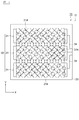
図1は本発明の第1実施形態における配線基板を示す平面図、図2は図1のII部の拡大平面図、図3は図2のIII-III線に沿った断面図、図4は図1において第1及び第2の断線部をマーキングした図である。<< First Embodiment >>
1 is a plan view showing a wiring board according to a first embodiment of the present invention, FIG. 2 is an enlarged plan view of a portion II in FIG. 1, FIG. 3 is a sectional view taken along line III-III in FIG. It is the figure which marked the 1st and 2nd disconnection part in FIG.
本実施形態における配線基板10(配線体11)は、図1〜図3に示すように、透明基板20と、当該透明基板20上に設けられた導体パターン30と、を備えている。なお、本実施形態における配線基板10が本発明における配線基板の一例に相当し、本実施形態における配線体11が本発明における配線体の一例に相当し、本実施形態における透明基板20が本発明における絶縁層の一例に相当し、本実施形態における導体パターン30が本発明における導体パターンの一例に相当する。
As shown in FIGS. 1 to 3, the wiring board 10 (wiring body 11) in the present embodiment includes a
透明基板20は、可視光線を透過することが可能であると共に電気絶縁性を有する透明な基板である。この透明基板20を構成する材料の具体例としては、例えば、ポリエチレンテレフタレート(PET)、ポリエチレンナフタレート(PEN)、ポリエチレン(PE)、ポリプロピレン(PP)、ポリスチレン(PS)、エチレン−酢酸ビニル共重合樹脂(EVA)、ビニル系樹脂、ポリカーボネート(PC)、ポリアミド(PA)、ポリイミド(PI)、ポリビニルアルコール(PVA)、アクリル樹脂、トリアセチルセルロース(TAC)等の樹脂材料を例示することができる。なお、樹脂材料に代えて、例えばガラスで透明基板20を構成してもよい。
The
導体パターン30は、図1に示すように、3つの帯状の検出電極31と、それぞれの検出電極31の両端に設けられた端部接続線32と、一方(図中右側)の端部接続線32から導出する引出線33と、を備えている。この導体パターン30は、図3に示すように、透明基板20の上面21に設けられている。なお、導体パターン30を構成する検出電極31の数は特に限定されない。
As shown in FIG. 1, the
それぞれの検出電極31は、図1及び図2に示すように、導電性を有する複数の第1の細線311,312を交差させて構成されており、全体として菱形を繰り返す網目形状を有している。本実施形態における検出電極31が本発明の検出電極の一例に相当し、本実施形態における第1の細線311,312が本発明における第1の細線の一例に相当する。
As shown in FIGS. 1 and 2, each
具体的には、一方の第1の細線311は、X軸方向に対して実質的に+45度の角度をなす方向(以下、単に「第1の方向」と称する。)に沿って直線状に延在しており、当該複数の第1の細線311は、この第1の方向に対して実質的に直交する方向(以下、単に「第2の方向」と称する。)に等ピッチP1で並べられている。他方の第1の細線312も、第2の方向に沿って直線状に延在しており、当該複数の第1の細線312は、第1の方向に等ピッチP2で並べられている。そして、これら第1の細線311,312が相互に直交することで、菱形状の単位網目313を繰り返す網目状の検出電極31が形成されている。本実施形態における検出電極31の単位網目313が、本発明における検出電極の単位網目の一例に相当する。Specifically, one of the first
なお、検出電極31を構成する単位網目313の数や配列は、特に限定されない。また、本実施形態では、第1の細線311のピッチP1と第1の細線312のピッチP2とを実質的に同一としているが(P1=P2)、特にこれに限定されない。第1の細線311のピッチP1と第2の細線312のピッチP2とを異ならせてもよい(P1≠P2)。また、X軸に対する第1の方向の角度やX軸に対する第2の方向の角度を、上記とは異なる角度としてもよい。Note that the number and arrangement of the unit meshes 313 constituting the
また、検出電極31を構成する単位網目313として、菱形以外の形状を用いてもよい。具体的には、三角形、菱形以外の四角形、六角形等のn角形、円、楕円、星形等を単位網目313として用いてもよいし、これらの中の複数の形状を単位網目313として用いてもよい。また、単位網目313の辺を直線以外の形状としてもよく、単位網目313の辺を、例えば、曲線、波線、ジグザグ線等にしてもよい。
Further, as the
さらに、図1〜図4に示すように、本実施形態における検出電極31は、その網目形状の中に第1の断線部314を含んでいる。この第1の断線部314では第1の細線311,312が除去されており(すなわち、この第1の断線部314では第1の細線311,312が未形成となっており)、第1の断線部314によって第1の細線311,312が電気的に切断されている。この第1の断線部314は、第1の細線311,312における交点315以外の箇所に形成されており、具体的には、第1の細線311,312において交点315の間の辺316の中央に形成されている。
Furthermore, as shown in FIGS. 1-4, the
なお、図4において、一点鎖線の丸枠に囲まれた箇所が第1の断線部314を示し、一点鎖線の矩形枠に囲まれた箇所が第3の断線部34(後述)を示している。また、本実施形態における第1の断線部314が本発明における第1の断線部の一例に相当し、本実施形態における第1の細線311,312の交点315が本発明における第1の細線の交点の一例に相当し、本実施形態における第1の細線311,312の辺316が本発明の第1の細線の辺の一例に相当する。因みに、本明細書において、後述する第2及び第3の断線部355,34を含む第1〜第3の断線部314,355,34とは、その断線部の延在方向において、当該断線部の長さL1〜L3が0.5μm以上であることを満たすものを示す。In FIG. 4, a portion surrounded by a dashed-dotted circle frame indicates a
こうした第1の断線部314を検出電極31に形成することで、複数の検出電極31間の境界線が目立ってしまうのを抑制することができ、この配線基板10を用いたタッチパネル1の視認性の向上を図ることができる。また、第1の断線部314を検出電極31に形成することで当該検出電極31の開口率を増加させることができるので、この配線基板10を用いてタッチパネルを構成した場合に、静電容量変化を大きくすることができ感度向上を図ることもできる。
By forming the
さらに、第1の断線部314を第1の細線311,312の辺316に形成することで、第1の細線311,312を交点315で断線させた場合と比較して、検出電極31において導通経路を多く確保することができ、電気的な抵抗値の増加を抑制することができる。
Further, by forming the
また、第1の断線部314を第1の細線311,312の辺316の中央に形成することで、第1の断線部314を第1の細線311,312の辺316の中央以外の部分に形成する場合と比較して、タッチパネル1の視認性がより向上する。
In addition, by forming the
本実施形態では、一つの単位網目313に対して、一つの第1の断線部314が形成されている。一つの単位網目313に第1の断線部314を複数形成すると、検出電極31を第1の断線部314によって分断され完全に断線してしまう場合がある。これに対し、一つの単位網目313に対して一つだけの第1の断線部314を形成することで、第1の断線部314によって検出電極31が分断されてしまうのを防止することができる。
In the present embodiment, one
なお、第1の断線部314が形成されていない単位網目313が存在してもよい。また、検出電極31の両端(すなわち端部接続線32)で電気的な導通を確保できるのであれば、検出電極31の中に複数の第1の断線部314が形成された単位網目313が存在してもよい。すなわち、第1の断線部314は、規則的に形成されていなくてもよい。
Note that there may be a
複数の検出電極31は、図1及び図4に示すように、相互に隣り合う検出電極31の第1の細線311,312の交点315(厳密には、相互に隣り合う検出電極31の第1の細線311,312の延長線上に存在する仮想上の交点315(図2参照))が一致するように並べられている。このため、導体パターン30全体において複数の検出電極31の網目形状が揃っている。
As shown in FIG. 1 and FIG. 4, the plurality of
さらに、本実施形態では、第3の断線部34が、相互に隣り合う検出電極31の第1の細線311,312の交点315に形成されている。この第3の断線部34では第1の細線311,312が除去されており(すなわち、この第3の断線部34では第1の細線311,312が未形成となっており)、この第3の断線部34によって、相互に隣り合う検出電極31が電気的に絶縁されている。
Furthermore, in this embodiment, the
こうした第3の断線部34を検出電極31間の交点315に形成することで、少ない第3の断線部34によって検出電極31間を効率的に断線することができ、複数の検出電極31の間の境界線が目立ってしまうのを抑制することができる。
By forming such
本実施形態では、検出電極31に形成された第1の断線部314の長さL1が、検出電極31間を分離する第3の断線部34の長さL3と実質的に同一となっている(L1=L3)。これにより、第3の断線部34が第1の断線部314に紛れて目立たなくなるので、この配線基板10を用いたタッチパネル1の視認性を一層向上させることができる。In the present embodiment, the length L 1 of the
導体パターン30は、導電性ペーストを透明基板20上に印刷して硬化させることで形成されている。導電性ペーストとしては、例えば、銀(Ag)や銅(Cu)等の金属粒子と、ポリエステルやポリフェノール等のバインダと、を混合したものを例示することができる。また、導電性ペーストの印刷方法としては、例えば、スクリーン印刷、グラビアオフセット印刷、インクジェット印刷等を例示することができる。
The
本実施形態では、導体パターン30を上記の印刷法により形成する際に、透明基板20上において第1の断線部314に対応する箇所に導電性ペーストを印刷しないことで、検出電極31内に第1の断線部314を形成する。同様に、透明基板20上において第3の断線部34に対応する箇所に導電性ペーストを印刷しないことで、検出電極31間に第3の断線部34を形成する。
In the present embodiment, when the
なお、例えば、透明基板20上に積層された金属層を網目状にパターニングすることで、導体パターン30を形成してもよい。或いは、スパッタリング法、真空蒸着法、化学蒸着法(CVD法)、無電解めっき法、電解めっき法、或いはそれらを組み合わせた方法を用いて、透明基板20上に導体パターン30を形成してもよい。
Note that, for example, the
また、第1及び第3の断線部314,34が形成されていない一様の網目状の電極を形成した後に、第1の細線311,312を部分的に削り取ることで、第1及び第3の断線部314,34を形成してもよい。
Moreover, after forming the uniform mesh-like electrode in which the 1st and
次に、以上に説明した配線基板10を用いたタッチパネル1の構造について、図5を参照しながら説明する。図5は本実施形態におけるタッチパネルを示す分解斜視図である。なお、以下に説明するタッチパネル1は静電容量方式のものであるが、特にこれに限定されず、例えば、配線基板10を抵抗膜方式のタッチパネルに使用してもよい。
Next, the structure of the
本実施形態におけるタッチパネル1は、パソコン、タブレット型情報端末、スマートフォン、カーナビゲーションシステム等の電子機器の入力装置として用いられる。こうした電子機器においてタッチパネル1は液晶ディスプレイ等の表示装置上に配置され、当該表示装置に表示された画面上の選択肢を、操作者が指で直接触れたり、専用のペンを用いて触れたりすることで、当該選択肢を選択することが可能となっている。
The
このタッチパネル1は、図5に示すように、カバー部材5と、2枚の配線基板10A,10Bと、を備えている。第1の配線基板10Aと第2の配線基板10Bは透明接着層を介して相互に貼り付けられており、カバー部材5と第2の配線基板10Bも透明接着層を介して相互に貼り付けられている。透明接着層を構成する粘着剤の具体例としては、例えば、アクリル系粘着剤等を例示することができる。
As shown in FIG. 5, the
カバー部材5は、上述の透明基板20と同様に、可視光線を透過することが可能であると共に電気絶縁性を有する透明な基板である。このカバー部材5の上面は、操作者による入力時に指やペンが接触する入力面として機能する。
The
第1の配線基板10Aは、上述した配線基板10を利用したものであり、図5中のY方向に沿って延在する帯状の第1の電極31Aを複数(本例では3つ)有しており、この複数の第1の電極31Aは相互に平行に並べられている。いずれの第1の電極31Aも、上述の電極31と同様に網目形状を有している。また、この複数の第1の電極31Aは、第1の引出線33Aを介して、タッチパネル駆動回路40に電気的に接続されている。
The
第2の配線基板10Bも、上述した配線基板10を利用したものであり、図5中のX方向に沿って延在する帯状の第2の電極31Bを複数(本例では3つ)有しており、この複数の第2の電極31Bは相互に平行に並べられている。いずれの第2の電極31Bも、上述の電極31と同様に網目形状を有している。また、この複数の第2の電極31Bは、第2の引出線33Bを介してタッチパネル駆動回路40に電気的に接続されている。
The
なお、第1の配線基板10Aと第2の配線基板10Bを重ねる際に、当該第1及び第2の配線基板10A,10Bの第1の断線部314同士が重ならないことが好ましく、これによりタッチパネル1の視認性が向上する。
In addition, when the
タッチパネル駆動回路40は、例えば、第1の電極31Aと第2の電極31Bとの間に所定電圧を周期的に印加し、第1及び第2の電極31A,31Bの交点毎の静電容量の変化に基づいてタッチパネル1上における指の位置を検出する。
For example, the touch
なお、第1の配線基板10A上の第1の電極31Aの数は特に限定されない。また、第2の配線基板10B上の第2の電極31Bの数も特に限定されない。
Note that the number of the
また、第1の配線基板10Aをカバー部材5と第2の配線基板10Bの間に配置してもよい。或いは、透明基板20に代えてカバー部材5に導体パターン30A(又は30B)を形成したり、一枚の透明基板20の両面に導体パターン30A,30Bを形成してもよい。
Further, the
以上のように、本実施形態では、第1の断線部314が検出電極31内の第1の細線311,312の交点315以外の箇所に設けられているので、タッチパネル1の電気的に接続の信頼性を維持しつつ視認性の向上を図ることができる。
As described above, in the present embodiment, the
≪第2実施形態≫
図6は本発明の第2実施形態における配線基板を示す平面図、図7は図6のVII部の拡大平面図、図8は図6において第1〜第3の断線部をマーキングした平面図である。<< Second Embodiment >>
6 is a plan view showing a wiring board according to the second embodiment of the present invention, FIG. 7 is an enlarged plan view of a VII portion in FIG. 6, and FIG. 8 is a plan view in which the first to third disconnected portions are marked in FIG. It is.
なお、図8において、一点鎖線の丸枠に囲まれた箇所が第1の断線部314を示し、一点鎖線の矩形枠に囲まれた箇所が第3の断線部34を示し、一点鎖線の菱形枠に囲まれた箇所が第2の断線部355(後述)を示している。
In FIG. 8, a portion surrounded by a dashed-dotted circle frame indicates the
本実施形態では、導体パターン30’の構成が第1実施形態と相違するが、それ以外の構成については第1実施形態と同様である。以下に、第2実施形態における配線基板10’(配線体11’)について第1実施形態との相違点についてのみ説明し、第1実施形態と同様の構成である部分については同一の符号を付してその説明を省略する。
In the present embodiment, the configuration of the
本実施形態における導体パターン30’は、検出電極31、端部接続線32及び引出線33に加えて、帯状のダミー電極35を備えている。検出電極31、端部接続線32及び引出線33の構成は、上述の第1実施形態で説明したものと同様であるので、これらの説明を省略する。
The
ダミー電極35は、図6〜図8に示すように、複数の検出電極31の間に介在しており、検出電極31の延在方向(図中のX方向)と同一の方向に帯状に延在している。それぞれのダミー電極35は、導電性を有する複数の第2の細線351,352を交差させて構成されており、全体として菱形を繰り返す網目形状を有している。本実施形態におけるダミー電極35が本発明におけるダミー電極の一例に相当し、本実施形態における第2の細線351,352が本発明における第2の細線の一例に相当する。
As shown in FIGS. 6 to 8, the
具体的には、一方の第2の細線351は、X軸方向に対して実質的に+45度の角度をなす方向(以下、単に「第1の方向」と称する。)に沿って直線状に延在しており、当該複数の第2の細線351は、この第1の方向に対して実質的に直交する方向(以下、単に「第2の方向」と称する。)に等ピッチP1で並べられている。他方の第2の細線352も、第2の方向に沿って直線状に延在しており、当該複数の第2の細線352は、第1の方向に等ピッチP2で並べられている。そして、これら第2の細線351,352が相互に直交することで、菱形状の単位網目353を繰り返す網目状のダミー電極35が形成されている。Specifically, one of the second
本実施形態では、第2の細線351のピッチP1が第1の細線311のピッチP1と実質的に同一であり、第2の細線352のピッチP2も第2の細線312のピッチP2と実質的に同一であり、結果的に、ダミー電極35の単位網目353は、上述の検出電極31の単位網目313と実質的に同一の形状を有している。In the present embodiment, the pitch P 1 of the second
なお、ダミー電極35を構成する単位網目353の数や配列は、特に限定されない。本実施形態におけるダミー電極35の単位網目353が、本発明におけるダミー電極の単位網目の一例に相当する。
Note that the number and arrangement of the unit nets 353 constituting the
検出電極31とダミー電極35は、図6及び図8に示すように、相互に隣り合う検出電極31とダミー電極35の第1及び第2の細線311,312,351,352の交点354(厳密には、相互に隣り合う検出電極31とダミー電極35の第1及び第2の細線311,312,351,352の延長線上に存在する仮想上の交点354(図6参照))が一致するように並べられている。このため、第2の導体パターン30’全体において検出電極31とダミー電極35の網目形状が揃っている。
As shown in FIGS. 6 and 8, the
さらに、本実施形態では、図7に示すように、第3の断線部34が、相互に隣り合う検出電極31とダミー電極35の第1及び第2の細線311,312,351,352の交点354に形成されている。この第3の断線部34では第1及び第2の細線311,312,351,352が除去されており(すなわち、この第3の断線部34では第1及び第2の細線311,312,311,312が未形成となっており)、この第3の断線部34によって、相互に隣り合う検出電極31とダミー電極35が電気的に絶縁されている。本実施形態における第3の断線部34が、本発明における第3の断線部の一例に相当する。
Furthermore, in the present embodiment, as shown in FIG. 7, the
こうした第3の断線部34を検出電極31とダミー電極35の間の交点354に形成することで、少ない第3の断線部34によって検出電極31とダミー電極35の間を効率的に断線することができ、検出電極31とダミー電極35の間の境界線が目立ってしまうのを抑制することができる。
By forming the
さらに、図6〜図8に示すように、本実施形態におけるダミー電極35は、その網目形状の中に第2の断線部355を含んでいる。この第2の断線部355では第2の細線351,352が除去されており(すなわち、この第2の断線部355では第2の細線351,352が未形成となっており)、第2の断線部355によって第2の細線351,352が電気的に切断されている。この第2の断線部355は、第2の細線351,352の交点356に形成されている。本実施形態における第2の断線部355が、本発明における第2の断線部の一例に相当する。
Further, as shown in FIGS. 6 to 8, the
こうした第2の断線部355をダミー電極35に形成することで、分割された個々の第2の細線351,352の面積が小さくなり、電荷が誘起され難くなるので、この配線基板10を用いたタッチパネルの感度向上を図ることもできる。
By forming the
また、第2の断線部355をダミー電極35内の交点356に形成することで、第2の細線351,352の辺に第2の断線部355を設けた場合と比較して、少ない第2の断線部355によってダミー電極35を効率的に断線すると共にダミー電極35を細かく分割することができる。
Further, by forming the
本実施形態では、検出電極31内に設けられた第1の断線部314の長さL1と、検出電極31とダミー電極35の間を分離する第3の断線部34の長さL3と、ダミー電極35内の第2の断線部355の長さL2と、が実質的に同一となっている(L1=L2=L3)。これにより、第3の断線部34が第1の断線部314や第2の断線部355に紛れて目立たなくなるので、この配線基板10’を用いたタッチパネルの視認性を一層向上させることができる。In the present embodiment, the length L 1 of the
ダミー電極35は、導電性ペーストを透明基板20上に印刷して硬化させることで形成されており、検出電極31、端部接続線32及び引出線33と同時に形成される。本実施形態では、導体パターン30’を上記の印刷法により形成する際に、透明基板20上において第2の断線部355に対応する箇所に導電性ペーストを印刷しないことで、ダミー電極35内に第2の断線部355を形成する。
The
以上のように、本実施形態では、上述の第1実施形態と同様に、第1の断線部314が検出電極31内の第1の細線311,312の交点315以外の箇所に形成されているので、タッチパネルの電気的に接続の信頼性を維持しつつ視認性の向上を図ることができる。
As described above, in the present embodiment, the
なお、本実施形態において、ダミー電極を構成する単位網目を、電極31の単位網目313と非同一な形状としてもよい。
In the present embodiment, the unit mesh constituting the dummy electrode may have a shape that is not identical to the
図9は本発明の第2実施形態における配線基板の変形例を示す平面図である。例えば、図9に示すように、ダミー電極35’を構成する単位網目を、検出電極31の単位網目313よりも小さな菱形としてもよい。この場合には、第2の断線部355によってダミー電極35’が一層細かく分割されるので、この配線基板10を用いたタッチパネルの感度をさらに向上させることができる。
FIG. 9 is a plan view showing a modification of the wiring board according to the second embodiment of the present invention. For example, as shown in FIG. 9, the unit mesh constituting the
また、図9に示す例のように、ダミー電極35において第2の細線351,352の辺に第2の断線部355Bを形成してもよい。
Further, as in the example illustrated in FIG. 9, the
また、第2の断線部355が形成されていない単位網目353が存在してもよい。ダミー電極35の中に複数の第2の断線部355が形成された単位網目353が存在してもよい。すなわち、第2の断線部355は、規則的に形成されていなくてもよい。
Further, there may be a
また、本実施形態では、第2の断線部355の数に対して第1の断線部314の数が相対的に少なくてもよい。
In the present embodiment, the number of the
≪第3実施形態≫
図10は本発明の第3実施形態における配線基板を示す平面図、図11は図10のXI部の拡大平面図である。«Third embodiment»
FIG. 10 is a plan view showing a wiring board according to the third embodiment of the present invention, and FIG. 11 is an enlarged plan view of a portion XI in FIG.
本実施形態では、配線基板10’’が配線体11’’と透明基板20を備え、配線体11’’が接着層50及び導体パターン30’’を備える点において第1実施形態と相違するが、それ以外の構成については第1実施形態と同様である。以下に、第3実施形態における配線体11’’を構成する接着層50及び配線基板10’’について説明し、第1実施形態と同様の構成である部分については同一の符号を付してその説明を省略する。なお、本実施形態における配線体11’’が本発明における配線体の一例に相当し、本実施形態における配線基板10’’が本発明における配線基板の一例に相当する。
This embodiment is different from the first embodiment in that the
接着層50は、透明基板20と導体パターン30’’とを相互に接着して固定するための層であり、透明基板20における上面21上の全体に設けられている。接着層50を構成する接着材料としては、エポキシ樹脂、アクリル樹脂、ポリエステル樹脂、ウレタン樹脂、ビニル樹脂、シリコーン樹脂、フェノール樹脂、ポリイミド樹脂等のUV硬化性樹脂、熱硬化性樹脂又は熱可塑性樹脂等を例示することができる。この接着層50は、導体パターン30’’を支持する支持部51(図12(e)参照)と、当該支持部51と透明基板20の上面21との間に設けられ、当該上面21を覆う平状部52(図12(e)参照)と、を有しており、それら支持部51及び平状部52は一体的に形成されている。本実施形態における接着層50が、本発明における絶縁層の一例に相当し、本実施形態における透明基板20が、本発明における基材の一例に相当する。
The
本実施形態における導体パターン30’’は、図10に示すように、検出電極31、端部接続線32、引出線33、及び、ダミー電極35’’を備えている。検出電極31、端部接続線32及び引出線33の構成は、上述の第1実施形態で説明したものと同様であるので、これらの説明を省略する。なお、上述の第2実施形態と同様に、検出電極31とダミー電極35’’とは、相互に電気的に絶縁されている。
As shown in FIG. 10, the
ダミー電極35’’では、当該ダミー電極35’’を構成する単位網目353’’が、検出電極31を構成する単位網目313と略同一の大きさとされた菱型から形成されている。また、このダミー電極35’’においては、第2の細線351’’、352’’の辺に第2の断線部355B’’が形成されている。
In the
本実施形態のダミー電極35’’は、当該ダミー電極35’’を構成する単位網目353’’が、検出電極31を構成する単位網目313に対して、当該検出電極31及びダミー電極35’’の並設方向に対して垂直な方向(すなわち、X方向)において相互にずれている点で、ダミー電極35と相違する。以下に、ダミー電極35とダミー電極35’’との相違点について、詳細に説明する。
In the
本実施形態の検出電極31を構成する単位網目313と、ダミー電極35’’を構成する単位網目353’’とは、以下のようにX方向において相互にずれている。すなわち、検出電極31を構成する第1の細線311は、ダミー電極35’’を構成する第2の細線351’’の仮想延長線(図中破線により表示)と実質的に不一致となるように配置されている。一方、検出電極31を構成する第1の細線312は、ダミー電極35’’を構成する第2の細線352’’の仮想延長線(図中破線により表示)と実質的に不一致となるように配置されている。
The
このように、検出電極31を構成する単位網目313と、ダミー電極35’’を構成する単位網目353’’とを、X方向において相互にずれて配置することで、当該検出電極31とダミー電極35’’とが相互に接近するのを防止し、検出電極31及びダミー電極35’’間が短絡するのを抑制することができる。
In this way, by disposing the
また、本実施形態では、検出電極31とダミー電極35’’とをY方向において離反するのではなく、単位網目313と単位網目353’’とをX方向において不揃いとすることで、これらを電気的に絶縁するので、第3の断線部34を必要としない。これにより、導体パターン30’’を用いた配線基板10’’(配線体11)の小型化を図ることができる。
In the present embodiment, the
なお、第1の断線部314が形成されていない単位網目313が存在してもよい。また、検出電極31の両端(すなわち端部接続線32)で電気的な導通を確保できるのであれば、検出電極31の中に複数の第1の断線部314が形成された単位網目313が存在してもよい。すなわち、第1の断線部314は、規則的に形成されていなくてもよい。
Note that there may be a
また、本実施形態では、第1の断線部314の割合は、電気的な抵抗値の抑制をする観点から、単位網目353’’が4個に対して、1個以下であることが好ましく、単位網目353’’が10個に対して、1個以下であることがより好ましい。ただし、第1の断線部314の割合は単位網目353’’が50個に対して、1個以上であった方がよい。
In the present embodiment, the ratio of the
また、本実施形態では、第2の断線部355B’’の数に対して第1の断線部314の数が相対的に少なくてもよい。例えば、第2の断線部355B’’に対する第1の断線部314の割合として、1/16個以下であると検出電極31の導電性を損なうことがなく好ましい。1/40個以下であるとさらに好ましい。また、1/200個以上であれば、視認性を向上する効果を発揮することができる。
In the present embodiment, the number of the
本実施形態では、第2の断線部355B’’の延在方向における長さL2が、第2の細線351’’,352’’の幅に対して相対的に大きいことが好ましく、下記(1)式が成立していることがさらに好ましい。
W2×5≧L2・・・(1)
但し、上記(1)式において、L2は第2の断線部355B’’の長さであり、W2は第2の細線351’’,352’’の幅である。In this embodiment, the
W 2 × 5 ≧ L 2 (1)
However, in the above equation (1), L 2 is the length of the
また、本実施形態の配線基板10’’では、下記(2)式が成立していることで、検出電極31が形成された領域の開口率と、ダミー電極35’’が形成された領域の開口率との間の差を小さくすることができるので、当該配線基板10’’を用いたタッチパネル1の視認性の向上をさらに図ることができる。
|A1―A2|≦1・・・(2)
但し、上記(2)式において、A1は検出電極31の開口率であり、A2はダミー電極35’’の開口率である。Further, in the
| A 1 −A 2 | ≦ 1 (2)
However, in the above formula (2), A 1 is the aperture ratio of the
さらに、本実施形態の配線基板10’’では、タッチパネル1の視認性を一層向上させる観点から、下記(3)式が成立していることがより好ましい。
|A1―A2|≦0.5・・・(3)Furthermore, in the
| A 1 −A 2 | ≦ 0.5 (3)
具体的には、第1及び第2の細線311,312,351’’,352’’の幅を2μmとする。また、第1の細線311,311間の中心間距離及び第2の細線351’’,351’’間の中心間距離であるピッチP1を92μmとする。同様に、第1の細線312,312間の中心間距離及び第2の細線352’’,352’’間の中心間距離であるピッチP2を92μmとする。また、第1の断線部314の長さL1及び第2の断線部355B’’の長さL2を5μmとする。そして、検出電極31においては、一つの単位網目313に対して、一つの第1の断線部314を形成する。一方、ダミー電極35’’においては、一つの単位網目353’’に対して、四つの第2の断線部355B’’を形成する。Specifically, the width of the first and second
上述の場合、検出電極31の開口率A1は、95.67%となるのに対して、ダミー電極35’’の開口率A2は、95.89%となる。つまり、検出電極31の開口率A1とダミー電極35’’の開口率A2との差の絶対値が0.22%となる(|A1―A2|=0.22)。このように、配線基板10’’が上記(3)式を満たすことで、タッチパネル1の視認性の向上がさらに図られる。If the above, the aperture ratio A 1 of the
なお、上記(1)〜(3)式は、上述した第2実施形態で説明した配線基板10’(配線体11’)においても、成立していることが好ましい。
It should be noted that the above equations (1) to (3) are preferably established also in the
また、本実施形態では、第1及び第2の細線311,351’’の延在方向は、第1の方向であり、第1及び第2の細線312,352’’の延在方向は、第2の方向であるが、このX軸に対する第1の方向の角度やX軸に対する第2の方向の角度を、第1実施形態で説明したものとは異なる角度としてもよい。
In the present embodiment, the extending direction of the first and second
本実施形態の導体パターン30’’は、第1実施形態で説明した導体パターン30を構成する材料と同様の材料により構成することができるが、特に上述に限定されない。具体的には、導体パターン30’’を構成する導電性ペーストとしては、金属粒子のほかに、導電性粉末や金属塩を用いることができる。導電性粉末としては、銀、銅、ニッケル、スズ、ビスマス、亜鉛、インジウム、パラジウム等の金属やグラファイト等例示することができる。金属塩としては、これらの金属の塩を挙げることができる。また、導電性ペーストに混合されるバインダとしては、上述した材料のほかに、アクリル樹脂、エポキシ樹脂、ビニル樹脂、ウレタン樹脂、フェノール樹脂、ポリイミド樹脂、等を用いることができる。
The
次に、配線基板10’’の製造方法について、詳細に説明する。図12(a)〜図12(e)は本発明の第3実施形態における配線基板の製造方法を説明するための平面図である。
Next, a method for manufacturing the
まず、図12(a)に示すように、導体パターン30’’の形状に対応する形状の凹部61が形成された凹版60を準備する。凹版60を構成する材料としては、ニッケル、シリコン、二酸化珪素、有機シリカ類、グラッシーカーボン、熱可塑性樹脂、光硬化性樹脂等を例示することができる。凹部61の幅は、通常50nm〜1000μmであるが、100nm〜100μmであることが好ましく、500nm〜10μmであることがより好ましい。また、凹部61の深さとしては、通常50nm〜3000μmであるが、100nm〜100μmことが好ましく500nm〜10μmであることがより好ましい。
First, as shown in FIG. 12A, an
凹部61の表面には、離型性を向上するために、黒鉛系材料、シリコーン系材料、フッ素系材料、セラミック系材料、アルミニウム系材料等からなる離型層を形成することが好ましい。
In order to improve the releasability, it is preferable to form a release layer made of a graphite material, a silicone material, a fluorine material, a ceramic material, an aluminum material, or the like on the surface of the
上記の凹版60の凹部61に対し、導電性材料70を充填する。このような導電性材料70としては、導電性粉末若しくは金属塩、バインダ、水若しくは溶剤及び各種の添加剤を混合して構成される導電性ペーストや導電性インクを例示することができる。上記の導電性粉末としては、銀や銅、ニッケル、スズ、ビスマス、亜鉛、インジウム、パラジウム等の金属やグラファイト等を例示することができる。金属塩としては、これらの金属の塩を挙げることができる。導電性材料70に含まれる導電性粒子としては、形成する導体パターンの幅に応じて、例えば、0.5μm以上2μm以下の直径φ(0.5≦φ≦2)を有する導電性粒子を用いることができる。なお、形成する導体パターンの幅の半分以下の平均直径φを有する導電性粒子を用いることが好ましい。
The
導電性材料70に含まれるバインダとしては、アクリル樹脂、ポリエステル樹脂、エポキシ樹脂、ビニル樹脂、ウレタン樹脂、フェノール樹脂、ポリイミド樹脂、等を挙げることができる。
Examples of the binder contained in the
導電性材料70に含まれる溶剤としては、α-テルピネオール、ブチルカルビトールアセテート、ブチルカルビトール、1−デカノール、ブチルセルソルブ、ジエチレングリコールモノエチルエーテルアセテート、テトラデカン等を例示することができる。
Examples of the solvent contained in the
導電性材料70を凹版60の凹部61に充填する方法としては、例えばディスペンス法、インクジェット法、スクリーン印刷法を挙げることができる。もしくはスリットコート法、バーコート法、ブレードコート法、ディップコート法、スプレーコート法、スピンコート法での塗工の後に凹部以外に塗工された導電性材料をふき取るもしくは掻き取る、吸い取る、貼り取る、洗い流す、吹き飛ばす方法を挙げることができる。導電性材料の組成等、凹版の形状等に応じて適宜使い分けることができる。本実施形態では、凹版60において、第1及び第2の断線部314,355B’’に対応する部分に凹部61を形成しないことで、導体パターン30’’内に第1及び第2の断線部314,355B’’に対応する形状が形成される。
Examples of the method of filling the
次に、図12(b)に示すように、凹版60の凹部61に充填された導電性材料70を加熱することにより導体パターン30’’を形成する。導電性材料70の加熱条件は、導電性材料の組成等に応じて適宜設定することができる。この加熱処理により、導電性材料70が体積収縮する。
Next, as shown in FIG. 12B, the
なお、導電性材料70の処理方法は加熱に限定されない。赤外線、紫外線、レーザー光等のエネルギー線を照射しても良いし、乾燥のみでもよい。また、これらの2種以上の処理方法を組合せても良い。
Note that the treatment method of the
続いて、図12(c)に示すように、接着層50を形成するための接着材料80が透明基板20上に略均一に塗布されたものを用意する。このような接着材料80としては、エポキシ樹脂、アクリル樹脂、ポリエステル樹脂、ウレタン樹脂、ビニル樹脂、シリコーン樹脂、フェノール樹脂、ポリイミド樹脂等のUV硬化性樹脂、熱硬化性樹脂又は熱可塑性樹脂等を例示することができる。
Subsequently, as shown in FIG. 12C, a material in which an
なお、接着層50を構成する材料の粘度は、塗布時の十分な流動性を確保する観点から、1mPa・s〜10,000mPa・sであることが好ましい。また、硬化後の樹脂の貯蔵弾性率は、導体パターン30’’の耐久性の観点から、106Pa以上、109Pa以下であることが好ましい。In addition, it is preferable that the viscosity of the material which comprises the
接着材料80を透明基板20上に塗布する方法としては、スクリーン印刷法、スプレーコート法、バーコート法、ディップ法、インクジェット法等を例示することができる。
Examples of the method for applying the
次いで、接着材料80が凹版60の凹部61に入り込むよう透明基板20及び接着材料80を凹版60上に配置して当該透明基板20及び接着材料80を凹版60に押し付け、接着材料80を硬化させる。透明基板20及び接着材料80を凹版60に押し付ける際の加圧力は、0.001MPa〜100MPaであることが好ましく、0.01MPa〜10MPaであることがより好ましい。なお、当該加圧は加圧ローラー等を用いて行うことができる。これにより、接着層50が形成されると共に、当該接着層50を介して透明基板20と導体パターン30’’とが相互に接着され固定される。
Next, the
接着材料80の硬化方法等は接着材料80の組成等により適宜設定することができる。例えば、加熱しても良く、乾燥のみでもよく、赤外線、紫外線レーザー光等のエネルギー線を照射しても良い。また、これらの2種以上の処理方法を組み合わせてもよい。なお、接着材料80として、熱可塑性材料を用いる場合には、熱等を加え溶融した後、冷却することにより、接着層50を形成することができる。
The curing method and the like of the
なお、接着層50の形成方法は特に上記に限定されない。例えば、接着層50が形成された凹版60(図12(b)に示す状態の凹版60)上に接着材料80を塗布し、当該接着材料80上に透明基板20を配置した後に、当該透明基板20を凹版60に配置して押し付けた状態で接着材料80を硬化することにより接着層50を形成してもよい。
The method for forming the
そして、当該透明基板20、接着層50及び導体パターン30を凹版60から離型し、本実施形態における配線体11’’を備えた配線基板10’’を得ることができる。
Then, the
なお、以上説明した実施形態は、本発明の理解を容易にするために記載されたものであって、本発明を限定するために記載されたものではない。したがって、上記の実施形態に開示された各要素は、本発明の技術的範囲に属する全ての設計変更や均等物をも含む趣旨である。 The embodiment described above is described for facilitating the understanding of the present invention, and is not described for limiting the present invention. Therefore, each element disclosed in the above embodiment is intended to include all design changes and equivalents belonging to the technical scope of the present invention.
上述の実施形態では、配線基板をタッチパネルに適用した例について説明したが、配線基板を適用可能な入力装置は特にこれに限定されない。 In the above-described embodiment, the example in which the wiring board is applied to the touch panel has been described. However, the input device to which the wiring board can be applied is not particularly limited thereto.
例えば、上述した配線基板10をタッチスイッチに適用してもよい。こうしたタッチスイッチの具体例としては、例えば、操作者の指やペンの接近や離反に伴う静電容量の変化に基づいてオン/オフを切り替えるスイッチ等を例示することができる。
For example, the
また、上述の第3実施形態で詳細に説明した配線基板の製造方法を用いて、第1及び第2実施形態で説明した導体パターン30,30’を備える配線基板を製造してもよい。この際、導体パターン30,30’を構成する材料としては、第3実施形態で例示したものを用いることができる。
In addition, a wiring board including the
また、上述の第3実施形態で説明した配線基板の製造方法を用いる場合、タッチパネル1としては、導体パターン30Aを有する配線基板10Aと、導体パターン30Bを有する10Bと、を備える構成(図5参照)に限定されない。具体的には、タッチパネルは、基材の一方主面側に二層の導体パターンを形成した配線体を備える配線基板(いわゆる、片面基板)により構成されていてもよい。このような配線基板は、以下のように製造する。
When the method for manufacturing a wiring board described in the third embodiment is used, the
すなわち、上述の第3実施形態で説明した方法により配線基板10’’を製造した後、導体パターン30’’を覆う樹脂層をさらに形成する。そして、形成された樹脂層を介して、導体パターン30’’と対向するように導体パターンをさらに形成する。
That is, after manufacturing the
本例の樹脂層を形成する方法としては、第3実施形態で説明した接着層50の形成方法と同様の方法を例示することができる。本例の導体パターンは、例えば、第3実施形態で説明した導体パターン30’’の形成方法と同様の方法により形成する。そして、配線基板10’’上に形成された本例の樹脂層を導体パターンに押し付け、当該樹脂層を硬化させることで、樹脂層上に導体パターンが形成される。なお、本例において、樹脂層上に導体パターンを形成する方法は、特に上述に限定されない。例えば、配線基板10’’上に形成された本例の樹脂層を硬化させた後、上述の第1実施形態で説明した導体パターン30を形成する方法を用いて当該樹脂層上に本例の導体パターンを形成してもよい。
As a method of forming the resin layer of this example, a method similar to the method of forming the
以上により、透明基板20の一方主面側に二層の導体パターンを形成した配線体を備える配線基板を得ることができる。タッチパネルは、この配線基板を備えた構成としてもよい。
By the above, a wiring board provided with the wiring body which formed the two-layered conductor pattern in the one main surface side of the
また、例えば、上述した第3実施形態における配線基板10’’から透明基板20を省略してもよい。この場合において、例えば、接着層50の下面に剥離シートを設け、実装時に当該剥離シートを剥がして実装対象(フィルム、表面ガラス、偏光板、ディスプレイ等)に接着して実装する形態として配線体又は配線基板を構成してもよい。なお、この形態では、接着層50が本発明の絶縁層の一例に相当し、実装対象が本発明の基材の一例に相当する。また、導体パターン30’’を覆う第2の接着層をさらに設け、当該第2の接着層を介して、上述の実装対象に接着して実装する形態として配線体又は配線基板を構成してもよい。この形態では、第2の接着層が本発明の絶縁層の一例に相当し、実装対象が本発明の基材の一例に該当する。
Further, for example, the
また、上述の第3実施形態における接着層50の平伏部52を基材として用いてもよい。この場合、接着層50が本発明の絶縁層及び基材の一例に相当する。
Moreover, you may use the
また、上述の実施形態では、配線体又は配線基板は、タッチパネル等のタッチセンサに用いられるとして説明したが、配線体又は配線基板の用途は特にこれに限定されない。たとえば、配線体に通電して抵抗加熱等で発熱させることにより当該配線体をヒーターとして用いてもよい。また、導体パターンの一部を接地することにより当該配線体を電磁遮蔽シールドとして用いてもよい。また、配線体をアンテナとして用いてもよい。 Moreover, although the wiring body or the wiring board was described as being used for a touch sensor such as a touch panel in the above-described embodiment, the use of the wiring body or the wiring board is not particularly limited thereto. For example, the wiring body may be used as a heater by energizing the wiring body and generating heat by resistance heating or the like. Alternatively, the wiring body may be used as an electromagnetic shielding shield by grounding a part of the conductor pattern. Moreover, you may use a wiring body as an antenna.
また、上述の実施形態の導電パターンは、導電性材料と、バインダ樹脂と、から構成されているが、当該導電パターンを構成する材料からバインダ樹脂を省略してもよい。 Moreover, although the conductive pattern of the above-mentioned embodiment is comprised from an electroconductive material and binder resin, you may abbreviate | omit binder resin from the material which comprises the said conductive pattern.
1…タッチパネル
5…カバー部材
10,10A,10B,10’,10’’…配線基板
20…透明基板
21…上面
11’’…配線体
30,30A,30B,30’,30’’…導体パターン
31,31A,31B…検出電極
311,312…第1の細線
313…単位網目
314…第1の断線部
315…交点
316…辺
32…端部接続線
33,33A,33B…引出線
34…第3の断線部
35,35’,35’’…ダミー電極
351,351’’,352,352’’…第2の細線
353,353’’…単位網目
354…交点
355,355B,355B’’…第2の断線部
356…交点
50…接着層
51…支持部
52…平伏部
40…駆動回路
60…凹版
61…凹部
70…導電性材料
80…接着材料DESCRIPTION OF
311, 312 ... 1st fine wire
313: Unit mesh
314 ... 1st disconnection part
315 ... Intersection
316:
351, 351 ″, 352, 352 ″ —second fine wire
353,353 '' ... Unit mesh
354 ... Intersection
355, 355B, 355B '' ... second disconnection
356...
Claims (12)
前記絶縁層上に設けられた導体パターンと、を備えた配線体であって、
前記導体パターンは、相互に並べられた複数の検出電極を備え、
前記検出電極は、複数の第1の細線を相互に交差させてなる網目状の検出電極であり、
前記検出電極は、前記第1の細線における交点以外の箇所に形成された第1の断線部を含み、
前記第1の断線部は、前記第1の細線における前記交点間の辺に形成され、
一方の前記交点と前記第1の断線部との間に前記辺の残部が存在していると共に、他方の交点と前記第1の断線部との間にも前記辺の残部が存在していることを特徴とする配線体。 An insulating layer;
A wiring body provided with a conductor pattern provided on the insulating layer,
The conductor pattern includes a plurality of detection electrodes arranged with each other,
Wherein the detection electrode is a mesh-like detection electrodes made by intersecting a plurality of first fine-line with each other,
Wherein the detection electrode is viewed including the first breaking portion formed on a portion other than the intersection of the first thin line,
The first disconnection part is formed on a side between the intersections in the first thin line,
The remaining part of the side exists between one of the intersections and the first disconnection part, and the remaining part of the side also exists between the other intersection and the first disconnection part. A wiring body characterized by that.
前記導体パターンは、複数の前記検出電極の間にそれぞれ介在し、複数の第2の細線を交差させてなる少なくとも一つの網目状のダミー電極を備えており、
前記ダミー電極は、少なくとも一つの第2の断線部を含むことを特徴とする配線体。 The wiring body according to claim 1,
Wherein the conductive pattern interposed respectively between the detection electrodes of the multiple comprises at least one mesh dummy electrodes made by intersecting a plurality of second fine wire,
The dummy body includes at least one second disconnection portion.
前記ダミー電極は、前記検出電極を構成する単位網目と実質的に同一の形状の単位網目から構成されていることを特徴とする配線体。 The wiring body according to claim 2,
The wiring body, wherein the dummy electrode is composed of a unit mesh having substantially the same shape as a unit mesh constituting the detection electrode.
前記検出電極を構成する単位網目と、前記ダミー電極を構成する単位網目とは、前記検出電極及び前記ダミー電極の並設方向に対して垂直な方向において相互にずれていることを特徴とする配線体。 The wiring body according to claim 3,
The unit mesh constituting the detection electrode and the unit mesh constituting the dummy electrode are shifted from each other in a direction perpendicular to the juxtaposition direction of the detection electrode and the dummy electrode. body.
前記第2の断線部の長さが、前記第2の細線の幅に対して相対的に大きいことを特徴とする配線体。 The wiring body according to any one of claims 2 to 4,
The length of the said 2nd disconnection part is relatively large with respect to the width | variety of a said 2nd thin wire | line, The wiring body characterized by the above-mentioned.
下記(1)式を満たすことを特徴とする配線体。
W2×5≧L2・・・(1)
但し、上記(1)式において、L2は前記第2の断線部の長さであり、W2は前記第2の細線の幅である。 The wiring body according to claim 5,
The wiring body characterized by satisfying the following expression (1).
W 2 × 5 ≧ L 2 (1)
However, in the above formula (1), L 2 is the length of the second disconnection part, and W 2 is the width of the second thin line.
下記(2)式を満たすことを特徴とする配線体。
|A1―A2|≦1・・・(2)
但し、上記(2)式において、A1は前記検出電極の開口率であり、A2は前記ダミー電極の開口率である。 The wiring body according to any one of claims 2 to 6,
The wiring body characterized by satisfying the following expression (2).
| A 1 −A 2 | ≦ 1 (2)
However, in the above equation (2), A 1 is the aperture ratio of the detection electrode, and A 2 is the aperture ratio of the dummy electrode.
前記第1の断線部は、前記第1の細線における前記交点間の前記辺の中央に形成されていることを特徴とする配線体。 The wiring body according to any one of claims 1 to 7,
It said first disconnection unit, wiring body, characterized in that it is formed in the center of the edges between the intersection of the first thin line.
前記検出電極を構成する一つの単位網目に対して、一つの前記第1の断線部が形成されていることを特徴とする配線体。 It is a wiring object given in any 1 paragraph of Claims 1-8,
The wiring body according to claim 1, wherein one first disconnection portion is formed for one unit network constituting the detection electrode.
前記導体パターンは、相互に隣り合う前記検出電極の前記第1の細線の交点に形成された少なくとも一つの第3の断線部を備えていることを特徴とする配線体。 The wiring body according to claim 1,
Wherein the conductive pattern wiring body, characterized in that it comprises at least one third disconnection portion formed at the intersection of the first thin line of the detection electrodes adjacent mutually.
前記導体パターンは、相互に隣り合う前記検出電極と前記ダミー電極の前記第1及び前記第2の細線の交点に形成された少なくとも一つの第3の断線部をさらに備えることを特徴とする配線体。 It is a wiring object given in any 1 paragraph of Claims 2-7,
The conductor pattern further includes at least one third disconnection portion formed at an intersection of the first and second thin wires of the detection electrode and the dummy electrode adjacent to each other. .
前記絶縁層は、前記導体パターンを支持する基材、または、前記導体パターンと基材を接着する接着層を構成することを特徴とする配線基板。 A wiring board comprising the wiring body according to any one of claims 1 to 11,
The said insulating layer comprises the base material which supports the said conductor pattern, or the contact bonding layer which adhere | attaches the said conductor pattern and a base material, The wiring board characterized by the above-mentioned.
Applications Claiming Priority (3)
| Application Number | Priority Date | Filing Date | Title |
|---|---|---|---|
| JP2014079240 | 2014-04-08 | ||
| JP2014079240 | 2014-04-08 | ||
| PCT/JP2015/060974 WO2015156316A1 (en) | 2014-04-08 | 2015-04-08 | Wiring body and wiring substrate |
Publications (2)
| Publication Number | Publication Date |
|---|---|
| JPWO2015156316A1 JPWO2015156316A1 (en) | 2017-04-13 |
| JP6200582B2 true JP6200582B2 (en) | 2017-09-20 |
Family
ID=54287890
Family Applications (1)
| Application Number | Title | Priority Date | Filing Date |
|---|---|---|---|
| JP2016512755A Expired - Fee Related JP6200582B2 (en) | 2014-04-08 | 2015-04-08 | Wiring body and wiring board |
Country Status (6)
| Country | Link |
|---|---|
| US (1) | US10025444B2 (en) |
| EP (1) | EP3130992A4 (en) |
| JP (1) | JP6200582B2 (en) |
| CN (1) | CN106133668B (en) |
| TW (1) | TWI610600B (en) |
| WO (1) | WO2015156316A1 (en) |
Families Citing this family (22)
| Publication number | Priority date | Publication date | Assignee | Title |
|---|---|---|---|---|
| KR102036426B1 (en) * | 2015-06-29 | 2019-10-24 | 미쓰비시 세이시 가부시키가이샤 | Light transmissive conductive material |
| TWI583748B (en) * | 2016-02-25 | 2017-05-21 | 財團法人工業技術研究院 | Circuit printing apparatus, circuit printing method and printed circuit structure |
| JP6143909B1 (en) * | 2016-03-29 | 2017-06-07 | 株式会社フジクラ | Wiring body, wiring board, touch sensor, and manufacturing method of wiring body |
| JP6577662B2 (en) * | 2016-03-30 | 2019-09-18 | 株式会社フジクラ | Wiring body, wiring board, and touch sensor |
| KR101929281B1 (en) | 2016-05-19 | 2019-03-15 | 삼성디스플레이 주식회사 | Electronic device |
| EP3487268A4 (en) * | 2016-07-12 | 2020-03-11 | Fujikura, Ltd. | Stretchable substrate |
| GB201613051D0 (en) | 2016-07-28 | 2016-09-14 | Landa Labs (2012) Ltd | Applying an electrical conductor to a substrate |
| JPWO2018123974A1 (en) * | 2016-12-28 | 2019-06-27 | 株式会社フジクラ | Wiring body, wiring board, and touch sensor |
| TWI652604B (en) | 2017-02-16 | 2019-03-01 | 日商阿爾普士電氣股份有限公司 | Static sensor and input device |
| KR101990343B1 (en) * | 2017-03-06 | 2019-06-18 | 후지필름 가부시키가이샤 | Touch panel, conductive sheet for touch panel and touch sensor |
| CN107584960B (en) * | 2017-07-26 | 2020-04-17 | 丁蒙蒙 | Sand painting performance equipment |
| JP2019079133A (en) * | 2017-10-20 | 2019-05-23 | 日本航空電子工業株式会社 | Touch panel |
| EP3720256A4 (en) | 2017-11-29 | 2021-11-17 | Dai Nippon Printing Co., Ltd. | Wiring board and production method for wiring board |
| CN110007808B (en) * | 2017-12-29 | 2022-10-18 | 乐金显示有限公司 | Electroluminescent display including touch sensor |
| CN108563364B (en) * | 2018-04-28 | 2024-03-08 | 京东方科技集团股份有限公司 | Touch screen, manufacturing method thereof, touch display panel and display device |
| KR101952770B1 (en) * | 2018-08-02 | 2019-02-27 | 동우 화인켐 주식회사 | Touch sensor |
| KR102561107B1 (en) | 2018-09-21 | 2023-07-27 | 엘지디스플레이 주식회사 | Touch display device |
| KR102147439B1 (en) * | 2018-10-17 | 2020-08-24 | 동우 화인켐 주식회사 | Antenna-deco film stack structure and display device including the same |
| CN109669576B (en) * | 2018-12-25 | 2022-04-15 | 业成科技(成都)有限公司 | Touch module |
| JP2020194215A (en) * | 2019-05-24 | 2020-12-03 | 日本航空電子工業株式会社 | Touch panel |
| CN111651094B (en) * | 2020-06-29 | 2023-07-28 | 合肥鑫晟光电科技有限公司 | Touch substrate and touch display device |
| WO2023188080A1 (en) * | 2022-03-30 | 2023-10-05 | シャープディスプレイテクノロジー株式会社 | Touch sensor and display device |
Family Cites Families (16)
| Publication number | Priority date | Publication date | Assignee | Title |
|---|---|---|---|---|
| JP4610416B2 (en) * | 2005-06-10 | 2011-01-12 | 日本写真印刷株式会社 | Capacitive touch panel |
| JP5253288B2 (en) | 2009-05-08 | 2013-07-31 | グンゼ株式会社 | Planar body and touch switch |
| CN104635983B (en) | 2008-07-31 | 2018-01-30 | 郡是株式会社 | Soft-touch control |
| JP5230533B2 (en) | 2009-05-29 | 2013-07-10 | 三菱電機株式会社 | Touch panel and display device having the same |
| JP5174745B2 (en) * | 2009-06-09 | 2013-04-03 | グンゼ株式会社 | Touch switch |
| JP2011059771A (en) * | 2009-09-07 | 2011-03-24 | Hitachi Chem Co Ltd | Mesh-shaped conductive pattern and base material with conductor layer pattern and touch panel member |
| JP2011059772A (en) | 2009-09-07 | 2011-03-24 | Hitachi Chem Co Ltd | Net-like conductive pattern, base material with conductive layer and touch panel member |
| KR101633034B1 (en) * | 2009-10-23 | 2016-06-24 | 삼성디스플레이 주식회사 | Touch substrate, method of manufacturing the same and display apparatus having the same |
| US8599150B2 (en) * | 2009-10-29 | 2013-12-03 | Atmel Corporation | Touchscreen electrode configuration |
| JP5667938B2 (en) | 2010-09-30 | 2015-02-12 | 富士フイルム株式会社 | Capacitive touch panel |
| CN103384870B (en) * | 2011-02-18 | 2016-06-01 | 富士胶片株式会社 | Conducting strip and contact panel |
| KR101634424B1 (en) | 2011-02-24 | 2016-06-28 | 후지필름 가부시키가이샤 | Electroconductive sheet and touch panel |
| KR101645828B1 (en) | 2011-12-16 | 2016-08-04 | 후지필름 가부시키가이샤 | Electroconductive sheet and touch panel |
| JP5875484B2 (en) * | 2011-12-22 | 2016-03-02 | 富士フイルム株式会社 | Conductive sheet and touch panel |
| JP5892419B2 (en) * | 2012-01-11 | 2016-03-23 | 大日本印刷株式会社 | Touch panel sensor |
| CN103425366B (en) | 2013-02-04 | 2016-08-03 | 南昌欧菲光科技有限公司 | Lead-in wire electrode and preparation method thereof |
-
2015
- 2015-04-08 JP JP2016512755A patent/JP6200582B2/en not_active Expired - Fee Related
- 2015-04-08 CN CN201580016833.XA patent/CN106133668B/en not_active Expired - Fee Related
- 2015-04-08 US US15/128,810 patent/US10025444B2/en not_active Expired - Fee Related
- 2015-04-08 TW TW104111195A patent/TWI610600B/en not_active IP Right Cessation
- 2015-04-08 EP EP15776277.4A patent/EP3130992A4/en not_active Withdrawn
- 2015-04-08 WO PCT/JP2015/060974 patent/WO2015156316A1/en active Application Filing
Also Published As
| Publication number | Publication date |
|---|---|
| EP3130992A4 (en) | 2018-01-17 |
| CN106133668A (en) | 2016-11-16 |
| TWI610600B (en) | 2018-01-01 |
| TW201607386A (en) | 2016-02-16 |
| CN106133668B (en) | 2019-03-26 |
| JPWO2015156316A1 (en) | 2017-04-13 |
| EP3130992A1 (en) | 2017-02-15 |
| WO2015156316A1 (en) | 2015-10-15 |
| US10025444B2 (en) | 2018-07-17 |
| US20170102804A1 (en) | 2017-04-13 |
Similar Documents
| Publication | Publication Date | Title |
|---|---|---|
| JP6200582B2 (en) | Wiring body and wiring board | |
| JP4346426B2 (en) | Narrow frame touch panel | |
| TWI657365B (en) | Wiring body, wiring board, and touch detector | |
| TW201013488A (en) | Planar element, and touch switch | |
| JP6346584B2 (en) | Touch panel and manufacturing method thereof | |
| JP6084117B2 (en) | Touch panel, display device and electronic device | |
| CN106126004B (en) | Touch panel and display device including the same | |
| WO2016002461A1 (en) | Input device and method for manufacturing same | |
| JP6085647B2 (en) | Wiring assembly, structure with conductor layer, and touch sensor | |
| WO2018181175A1 (en) | Wiring body, wiring substrate, and touch sensor | |
| US20200064971A1 (en) | Wiring body assembly, wiring board, and touch sensor | |
| KR20160042617A (en) | Conductive film and method for manufacturing the same, and touch panel and display apparatus including the conductive film | |
| JP2014112356A (en) | Touch panel | |
| JP6440526B2 (en) | Wiring body | |
| JP6180174B2 (en) | Touch panel, display device and electronic device | |
| JP2020064403A (en) | Wiring body, wiring board, and touch sensor | |
| JP6034932B1 (en) | Wiring body, wiring board, and touch sensor | |
| JP2018124615A (en) | Wiring body, wiring substrate and touch sensor | |
| JP6207555B2 (en) | Wiring body, structure with conductor layer, and touch sensor | |
| JP6549942B2 (en) | Wiring body, wiring board, and touch sensor | |
| JP2018110153A (en) | Wiring body assembly, wiring board, and touch sensor | |
| JP2020091582A (en) | Wiring body and wiring board and touch sensor | |
| JP2020047172A (en) | Wiring body, wiring board, and touch sensor | |
| JP2018110152A (en) | Wiring body assembly, wiring board, and touch sensor | |
| JP2020047173A (en) | Wiring body, wiring board, and touch sensor |
Legal Events
| Date | Code | Title | Description |
|---|---|---|---|
| A131 | Notification of reasons for refusal |
Free format text: JAPANESE INTERMEDIATE CODE: A131 Effective date: 20170221 |
|
| A601 | Written request for extension of time |
Free format text: JAPANESE INTERMEDIATE CODE: A601 Effective date: 20170419 |
|
| A521 | Written amendment |
Free format text: JAPANESE INTERMEDIATE CODE: A523 Effective date: 20170621 |
|
| TRDD | Decision of grant or rejection written | ||
| A01 | Written decision to grant a patent or to grant a registration (utility model) |
Free format text: JAPANESE INTERMEDIATE CODE: A01 Effective date: 20170815 |
|
| A61 | First payment of annual fees (during grant procedure) |
Free format text: JAPANESE INTERMEDIATE CODE: A61 Effective date: 20170825 |
|
| R151 | Written notification of patent or utility model registration |
Ref document number: 6200582 Country of ref document: JP Free format text: JAPANESE INTERMEDIATE CODE: R151 |
|
| LAPS | Cancellation because of no payment of annual fees |