KR20140048178A - Method of manufacutruing semiconductor device structure - Google Patents
Method of manufacutruing semiconductor device structure Download PDFInfo
- Publication number
- KR20140048178A KR20140048178A KR1020140037948A KR20140037948A KR20140048178A KR 20140048178 A KR20140048178 A KR 20140048178A KR 1020140037948 A KR1020140037948 A KR 1020140037948A KR 20140037948 A KR20140037948 A KR 20140037948A KR 20140048178 A KR20140048178 A KR 20140048178A
- Authority
- KR
- South Korea
- Prior art keywords
- semiconductor device
- device structure
- semiconductor
- encapsulant
- manufacturing
- Prior art date
Links
- 239000004065 semiconductor Substances 0.000 title claims abstract description 177
- 238000000034 method Methods 0.000 title claims abstract description 37
- 238000004519 manufacturing process Methods 0.000 claims abstract description 47
- 239000000463 material Substances 0.000 claims abstract description 16
- 239000008393 encapsulating agent Substances 0.000 claims description 55
- 239000003795 chemical substances by application Substances 0.000 claims description 9
- 238000007789 sealing Methods 0.000 claims description 9
- 238000003825 pressing Methods 0.000 claims description 8
- 238000005538 encapsulation Methods 0.000 abstract 3
- 239000000758 substrate Substances 0.000 description 18
- OAICVXFJPJFONN-UHFFFAOYSA-N Phosphorus Chemical compound [P] OAICVXFJPJFONN-UHFFFAOYSA-N 0.000 description 8
- 239000000853 adhesive Substances 0.000 description 7
- 230000001070 adhesive effect Effects 0.000 description 6
- 238000010586 diagram Methods 0.000 description 5
- 239000002184 metal Substances 0.000 description 5
- 229910052594 sapphire Inorganic materials 0.000 description 5
- 239000010980 sapphire Substances 0.000 description 5
- 230000006798 recombination Effects 0.000 description 4
- 238000005215 recombination Methods 0.000 description 4
- 229910004298 SiO 2 Inorganic materials 0.000 description 3
- 238000009792 diffusion process Methods 0.000 description 3
- 150000004767 nitrides Chemical class 0.000 description 3
- 229920005989 resin Polymers 0.000 description 3
- 239000011347 resin Substances 0.000 description 3
- 230000004888 barrier function Effects 0.000 description 2
- 238000000605 extraction Methods 0.000 description 2
- 230000017525 heat dissipation Effects 0.000 description 2
- 238000000206 photolithography Methods 0.000 description 2
- 238000007650 screen-printing Methods 0.000 description 2
- 238000000926 separation method Methods 0.000 description 2
- 239000002904 solvent Substances 0.000 description 2
- 238000004528 spin coating Methods 0.000 description 2
- 239000004593 Epoxy Substances 0.000 description 1
- BPQQTUXANYXVAA-UHFFFAOYSA-N Orthosilicate Chemical compound [O-][Si]([O-])([O-])[O-] BPQQTUXANYXVAA-UHFFFAOYSA-N 0.000 description 1
- XUIMIQQOPSSXEZ-UHFFFAOYSA-N Silicon Chemical compound [Si] XUIMIQQOPSSXEZ-UHFFFAOYSA-N 0.000 description 1
- 229910010413 TiO 2 Inorganic materials 0.000 description 1
- 239000002390 adhesive tape Substances 0.000 description 1
- 239000011324 bead Substances 0.000 description 1
- 150000001875 compounds Chemical class 0.000 description 1
- 238000000748 compression moulding Methods 0.000 description 1
- 238000007796 conventional method Methods 0.000 description 1
- 238000005137 deposition process Methods 0.000 description 1
- 238000001312 dry etching Methods 0.000 description 1
- 239000003822 epoxy resin Substances 0.000 description 1
- 238000005530 etching Methods 0.000 description 1
- 239000011521 glass Substances 0.000 description 1
- 230000009477 glass transition Effects 0.000 description 1
- 238000009616 inductively coupled plasma Methods 0.000 description 1
- 230000001678 irradiating effect Effects 0.000 description 1
- 230000031700 light absorption Effects 0.000 description 1
- 239000007788 liquid Substances 0.000 description 1
- 238000002844 melting Methods 0.000 description 1
- 230000008018 melting Effects 0.000 description 1
- 238000000465 moulding Methods 0.000 description 1
- 238000005192 partition Methods 0.000 description 1
- 229920000647 polyepoxide Polymers 0.000 description 1
- 229920001296 polysiloxane Polymers 0.000 description 1
- 230000001376 precipitating effect Effects 0.000 description 1
- 238000005488 sandblasting Methods 0.000 description 1
- 229910052710 silicon Inorganic materials 0.000 description 1
- 239000010703 silicon Substances 0.000 description 1
- 229920001187 thermosetting polymer Polymers 0.000 description 1
Images


Classifications
-
- H—ELECTRICITY
- H01—ELECTRIC ELEMENTS
- H01L—SEMICONDUCTOR DEVICES NOT COVERED BY CLASS H10
- H01L24/00—Arrangements for connecting or disconnecting semiconductor or solid-state bodies; Methods or apparatus related thereto
- H01L24/93—Batch processes
- H01L24/95—Batch processes at chip-level, i.e. with connecting carried out on a plurality of singulated devices, i.e. on diced chips
- H01L24/96—Batch processes at chip-level, i.e. with connecting carried out on a plurality of singulated devices, i.e. on diced chips the devices being encapsulated in a common layer, e.g. neo-wafer or pseudo-wafer, said common layer being separable into individual assemblies after connecting
-
- H—ELECTRICITY
- H01—ELECTRIC ELEMENTS
- H01L—SEMICONDUCTOR DEVICES NOT COVERED BY CLASS H10
- H01L21/00—Processes or apparatus adapted for the manufacture or treatment of semiconductor or solid state devices or of parts thereof
- H01L21/02—Manufacture or treatment of semiconductor devices or of parts thereof
- H01L21/04—Manufacture or treatment of semiconductor devices or of parts thereof the devices having potential barriers, e.g. a PN junction, depletion layer or carrier concentration layer
- H01L21/50—Assembly of semiconductor devices using processes or apparatus not provided for in a single one of the subgroups H01L21/06 - H01L21/326, e.g. sealing of a cap to a base of a container
- H01L21/56—Encapsulations, e.g. encapsulation layers, coatings
- H01L21/568—Temporary substrate used as encapsulation process aid
-
- H—ELECTRICITY
- H01—ELECTRIC ELEMENTS
- H01L—SEMICONDUCTOR DEVICES NOT COVERED BY CLASS H10
- H01L2224/00—Indexing scheme for arrangements for connecting or disconnecting semiconductor or solid-state bodies and methods related thereto as covered by H01L24/00
- H01L2224/01—Means for bonding being attached to, or being formed on, the surface to be connected, e.g. chip-to-package, die-attach, "first-level" interconnects; Manufacturing methods related thereto
- H01L2224/02—Bonding areas; Manufacturing methods related thereto
- H01L2224/04—Structure, shape, material or disposition of the bonding areas prior to the connecting process
- H01L2224/04105—Bonding areas formed on an encapsulation of the semiconductor or solid-state body, e.g. bonding areas on chip-scale packages
-
- H—ELECTRICITY
- H01—ELECTRIC ELEMENTS
- H01L—SEMICONDUCTOR DEVICES NOT COVERED BY CLASS H10
- H01L2224/00—Indexing scheme for arrangements for connecting or disconnecting semiconductor or solid-state bodies and methods related thereto as covered by H01L24/00
- H01L2224/01—Means for bonding being attached to, or being formed on, the surface to be connected, e.g. chip-to-package, die-attach, "first-level" interconnects; Manufacturing methods related thereto
- H01L2224/18—High density interconnect [HDI] connectors; Manufacturing methods related thereto
- H01L2224/19—Manufacturing methods of high density interconnect preforms
-
- H—ELECTRICITY
- H01—ELECTRIC ELEMENTS
- H01L—SEMICONDUCTOR DEVICES NOT COVERED BY CLASS H10
- H01L2224/00—Indexing scheme for arrangements for connecting or disconnecting semiconductor or solid-state bodies and methods related thereto as covered by H01L24/00
- H01L2224/01—Means for bonding being attached to, or being formed on, the surface to be connected, e.g. chip-to-package, die-attach, "first-level" interconnects; Manufacturing methods related thereto
- H01L2224/18—High density interconnect [HDI] connectors; Manufacturing methods related thereto
- H01L2224/23—Structure, shape, material or disposition of the high density interconnect connectors after the connecting process
- H01L2224/24—Structure, shape, material or disposition of the high density interconnect connectors after the connecting process of an individual high density interconnect connector
- H01L2224/241—Disposition
- H01L2224/24135—Connecting between different semiconductor or solid-state bodies, i.e. chip-to-chip
- H01L2224/24137—Connecting between different semiconductor or solid-state bodies, i.e. chip-to-chip the bodies being arranged next to each other, e.g. on a common substrate
-
- H—ELECTRICITY
- H01—ELECTRIC ELEMENTS
- H01L—SEMICONDUCTOR DEVICES NOT COVERED BY CLASS H10
- H01L2224/00—Indexing scheme for arrangements for connecting or disconnecting semiconductor or solid-state bodies and methods related thereto as covered by H01L24/00
- H01L2224/01—Means for bonding being attached to, or being formed on, the surface to be connected, e.g. chip-to-package, die-attach, "first-level" interconnects; Manufacturing methods related thereto
- H01L2224/42—Wire connectors; Manufacturing methods related thereto
- H01L2224/47—Structure, shape, material or disposition of the wire connectors after the connecting process
- H01L2224/48—Structure, shape, material or disposition of the wire connectors after the connecting process of an individual wire connector
- H01L2224/4805—Shape
- H01L2224/4809—Loop shape
- H01L2224/48091—Arched
-
- H—ELECTRICITY
- H01—ELECTRIC ELEMENTS
- H01L—SEMICONDUCTOR DEVICES NOT COVERED BY CLASS H10
- H01L2224/00—Indexing scheme for arrangements for connecting or disconnecting semiconductor or solid-state bodies and methods related thereto as covered by H01L24/00
- H01L2224/01—Means for bonding being attached to, or being formed on, the surface to be connected, e.g. chip-to-package, die-attach, "first-level" interconnects; Manufacturing methods related thereto
- H01L2224/42—Wire connectors; Manufacturing methods related thereto
- H01L2224/47—Structure, shape, material or disposition of the wire connectors after the connecting process
- H01L2224/48—Structure, shape, material or disposition of the wire connectors after the connecting process of an individual wire connector
- H01L2224/481—Disposition
- H01L2224/48151—Connecting between a semiconductor or solid-state body and an item not being a semiconductor or solid-state body, e.g. chip-to-substrate, chip-to-passive
- H01L2224/48221—Connecting between a semiconductor or solid-state body and an item not being a semiconductor or solid-state body, e.g. chip-to-substrate, chip-to-passive the body and the item being stacked
- H01L2224/48245—Connecting between a semiconductor or solid-state body and an item not being a semiconductor or solid-state body, e.g. chip-to-substrate, chip-to-passive the body and the item being stacked the item being metallic
- H01L2224/48247—Connecting between a semiconductor or solid-state body and an item not being a semiconductor or solid-state body, e.g. chip-to-substrate, chip-to-passive the body and the item being stacked the item being metallic connecting the wire to a bond pad of the item
-
- H—ELECTRICITY
- H01—ELECTRIC ELEMENTS
- H01L—SEMICONDUCTOR DEVICES NOT COVERED BY CLASS H10
- H01L2224/00—Indexing scheme for arrangements for connecting or disconnecting semiconductor or solid-state bodies and methods related thereto as covered by H01L24/00
- H01L2224/01—Means for bonding being attached to, or being formed on, the surface to be connected, e.g. chip-to-package, die-attach, "first-level" interconnects; Manufacturing methods related thereto
- H01L2224/42—Wire connectors; Manufacturing methods related thereto
- H01L2224/47—Structure, shape, material or disposition of the wire connectors after the connecting process
- H01L2224/48—Structure, shape, material or disposition of the wire connectors after the connecting process of an individual wire connector
- H01L2224/484—Connecting portions
- H01L2224/4847—Connecting portions the connecting portion on the bonding area of the semiconductor or solid-state body being a wedge bond
- H01L2224/48472—Connecting portions the connecting portion on the bonding area of the semiconductor or solid-state body being a wedge bond the other connecting portion not on the bonding area also being a wedge bond, i.e. wedge-to-wedge
Landscapes
- Engineering & Computer Science (AREA)
- Computer Hardware Design (AREA)
- Microelectronics & Electronic Packaging (AREA)
- Power Engineering (AREA)
- Led Device Packages (AREA)
- Led Devices (AREA)
Abstract
Description
본 개시(Disclosure)는 전체적으로 반도체 소자 구조물을 제조하는 방법에 관한 것으로, 특히 제조가 간단한 반도체 소자 구조물을 제조하는 방법에 관한 것이다.Disclosure relates generally to a method of manufacturing a semiconductor device structure, and more particularly, to a method of manufacturing a semiconductor device structure that is simple to manufacture.
여기기, 반도체 소자라 함은 반도체 발광소자(예: 레이저 다이오드), 반도체 수광소자(예: 포토 다이오드), p-n접합 다이오드 전기 소자, 반도체 트랜지스터 등을 포함하며, 대표적으로 3족 질화물 반도체 발광소자를 예로 들 수 있다. 3족 질화물 반도체 발광소자는 Al(x)Ga(y)In(1-x-y)N (0≤x≤1, 0≤y≤1, 0≤x+y≤1)로 된 화합물 반도체층을 포함하는 발광다이오드와 같은 발광소자를 의미하며, 추가적으로 SiC, SiN, SiCN, CN와 같은 다른 족(group)의 원소들로 물질이나 이들 물질로 된 반도체층을 포함하는 것을 배제하는 것은 아니다.Here, the semiconductor device includes a semiconductor light emitting device (eg, a laser diode), a semiconductor light receiving device (eg, a photodiode), a pn junction diode electric device, a semiconductor transistor, and the like, and typically includes a group III nitride semiconductor light emitting device. Can be mentioned. The group III nitride semiconductor light emitting device includes a compound semiconductor layer of Al (x) Ga (y) In (1-xy) N (0 ≦ x ≦ 1, 0 ≦ y ≦ 1, 0 ≦ x + y ≦ 1). It means a light emitting device such as a light emitting diode, and does not exclude the inclusion of a material or a semiconductor layer of these materials with elements of other groups such as SiC, SiN, SiCN, CN.
여기서는, 본 개시에 관한 배경기술이 제공되며, 이들이 반드시 공지기술을 의미하는 것은 아니다(This section provides background information related to the present disclosure which is not necessarily prior art).Herein, the background art relating to the present disclosure is provided, and these are not necessarily meant to be known arts.
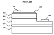
도 1은 종래의 반도체 발광소자의 일 예(Lateral Chip)를 나타내는 도면으로서, 반도체 발광소자는 기판(100), 기판(100) 위에, 버퍼층(200), 제1 도전성을 가지는 제1 반도체층(300), 전자와 정공의 재결합을 통해 빛을 생성하는 활성층(400), 제1 도전성과 다른 제2 도전성을 가지는 제2 반도체층(500)이 순차로 증착되어 있으며, 그 위에 전류 확산을 위한 투광성 전도막(600)과, 본딩 패드로 역할하는 전극(700)이 형성되어 있고, 식각되어 노출된 제1 반도체층(300) 위에 본딩 패드로 역할하는 전극(800)이 형성되어 있다. 여기서, 기판(100) 측이 패키지에 놓일 때, 장착면으로 기능한다.1 is a view illustrating a conventional semiconductor light emitting device (Lateral Chip), the semiconductor light emitting device is a
도 2는 종래의 반도체 발광소자의 다른 예(Flip Chip)를 나타내는 도면으로서, 반도체 발광소자는 기판(100; 예: 사파이어 기판), 기판(100) 위에, 제1 도전성을 가지는 제1 반도체층(300; 예: n형 GaN층), 전자와 정공의 재결합을 통해 빛을 생성하는 활성층(400; 예: InGaN/(In)GaN MQWs), 제1 도전성과 다른 제2 도전성을 가지는 제2 반도체층(500; 예: p형 GaN층)이 순차로 증착되어 있으며, 그 위에 기판(100) 측으로 빛을 반사시키기 위한 3층으로 된 전극막(901; 예: Ag 반사막), 전극막(902; 예: Ni 확산 방지막) 및 전극막(903; 예: Au 본딩층)이 형성되어 있고, 식각되어 노출된 제1 반도체층(300) 위에 본딩 패드로 기능하는 전극(800; 예: Cr/Ni/Au 적층 금속 패드)이 형성되어 있다. 여기서, 전극막(903) 측이 패키지에 놓일 때, 장착면으로 기능한다. 열방출 효율의 관점에서, 도 1에 도시된 래터럴 칩(Lateral Chip)보다 도 2에 도시된 플립 칩(Flip Chip) 또는 정션 다운형(Junction Down Type) 칩이 열방출 효율이 우수하다. 래터럴 칩이 80~180㎛의 두께를 가지는 사파이어 기판(100)을 통해 열을 외부로 방출해야 하는 반면에, 플립 칩은 활성층(400)에 가깝게 위치하는 금속으로 된 전극(901,902,903)을 통해 열을 방출할 수 있기 때문이다.FIG. 2 is a diagram illustrating another example of a conventional semiconductor light emitting device, wherein the semiconductor light emitting device includes a substrate 100 (eg, a sapphire substrate) and a first semiconductor layer having a first conductivity on the
도 15는 종래의 반도체 발광소자 패키지 또는 반도체 발광소자 구조물의 일 예를 나타내는 도면으로서, 반도체 발광소자 패키지는 리드 프레임(110,120), 몰드(130), 그리고 캐비티(140) 내에 수직형 반도체 발광소자(150; Vertical Type Light-emitting Chip)가 구비되어 있고, 캐비티(140)는 형광체(160)를 함유하는 봉지제(170)로 채워져 있다. 수직형 반도체 발광소자(150)의 하면이 리드 프레임(110)에 전기적으로 연결되고, 상면이 와이어(180)에 의해 리드 프레임(120)에 전기적으로 연결되어 있다. 수직형 반도체 발광소자(150)에서 나온 광(예: 청색광)의 일부가 형광체(160)를 여기시켜 형광체(160)가 광(예: 황색광)을 만들고, 이 광들(청색광+황색광)이 백색광을 만든다. 여기서, 몰드(130)-봉지제(170) 또는 리드 프레임(110,120)-몰드(130)-봉지제(170)가 수직형 반도체 발광소자를 담지한 채로, 반도체 발광소자 패키지의 지지체 즉, 캐리어(Carrier)로 역할한다.15 is a view showing an example of a conventional semiconductor light emitting device package or semiconductor light emitting device structure, the semiconductor light emitting device package is a vertical semiconductor light emitting device (in the
이에 대하여 '발명의 실시를 위한 구체적인 내용'의 후단에 기술한다.This will be described later in the Specification for Implementation of the Invention.
여기서는, 본 개시의 전체적인 요약(Summary)이 제공되며, 이것이 본 개시의 외연을 제한하는 것으로 이해되어서는 아니된다(This section provides a general summary of the disclosure and is not a comprehensive disclosure of its full scope or all of its features).SUMMARY OF THE INVENTION Herein, a general summary of the present disclosure is provided, which should not be construed as limiting the scope of the present disclosure. of its features).
본 개시에 따른 일 태양에 의하면(According to one aspect of the present disclosure), 반도체 소자 구조물을 제조하는 방법에 있어서, 플레이트 위에 반도체 소자를 위치 고정하는 단계;로서, 반도체 소자의 전극이 플레이트를 향하도록 위치 고정하는 단계; 반도체 소자를 봉지제로 덮는 단계; 봉지제가 덮힌 반도체 소자를 플레이트로부터 분리하는 단계; 그리고, 반도체 소자의 전극이 위치하는 측 및 봉지제의 상측 중의 적어도 일 측을 가압하여 요철을 형성하는 단계;를 포함하는 것을 특징으로 하는 반도체 소자 구조물을 제조하는 방법이 제공된다.According to one aspect of the present disclosure, there is provided a method of fabricating a semiconductor device structure, the method comprising: positioning a semiconductor device on a plate such that the electrode of the semiconductor device faces the plate; Fixing the position; Covering the semiconductor element with an encapsulant; Separating the semiconductor device covered with the encapsulant from the plate; And pressing at least one of the side where the electrode of the semiconductor element is located and the upper side of the encapsulant to form the unevenness. The method of manufacturing a semiconductor device structure is provided.
이에 대하여 '발명의 실시를 위한 구체적인 내용'의 후단에 기술한다.This will be described later in the Specification for Implementation of the Invention.
도 1은 종래의 반도체 발광소자의 일 예(Lateral Chip)를 나타내는 도면,
도 2는 종래의 반도체 발광소자의 다른 예(Flip Chip)를 나타내는 도면,
도 3은 본 개시에 따라 반도체 소자 구조물을 제조하는 방법의 일 예를 나타내는 도면,
도 4는 본 개시에 따라 플립 칩 패키지를 제조하는 방법의 일 예를 나타내는 도면,
도 5는 본 개시에 따라 반도체 소자 구조물을 제조하는 방법의 다른 예를 나타내는 도면,
도 6은 본 개시에 따른 반도체 소자 구조물의 일 예를 나타내는 도면,
도 7은 본 개시에 따라 반도체 소자 구조물을 제조하는 방법의 또 다른 예를 나타내는 도면,
도 8은 본 개시에 따른 반도체 소자 구조물의 다른 예를 나타내는 도면,
도 9는 본 개시에 따른 반도체 소자 구조물 사용의 일 예를 나타내는 도면,
도 10은 본 개시에 따라 반도체 소자 구조물을 제조하는 방법의 또 다른 예를 나타내는 도면,
도 11은 본 개시에 따른 반도체 소자 구조물의 또 다른 예를 나타내는 도면,
도 12은 본 개시에 따른 반도체 소자 구조물의 또 다른 예를 나타내는 도면,
도 13은 본 개시에 따른 반도체 소자 구조물의 또 다른 예를 나타내는 도면,
도 14는 본 개시에 따른 반도체 소자 구조물의 또 다른 예를 나타내는 도면,
도 15는 종래의 반도체 발광소자 패키지 또는 반도체 발광소자 구조물의 일 예를 나타내는 도면,
도 16은 본 개시에 따른 반도체 소자 구조물의 또 다른 예를 나타내는 도면,
도 17은 도 16에 제시된 반도체 소자 구조물을 제조하는 방법의 일 예를 나타내는 도면,
도 18은 도 16에 제시된 반도체 소자 구조물을 제조하는 방법의 다른 예를 나타내는 도면,
도 19는 도 16에 제시된 반도체 소자 구조물을 제조하는 과정에서 봉지제를 경화하는 공정의 일 예를 나타내는 도면.1 is a view showing an example of a conventional semiconductor light emitting device (lateral chip)
2 is a view showing another example (Flip Chip) of a conventional semiconductor light emitting device,
3 illustrates an example of a method of manufacturing a semiconductor device structure according to the present disclosure;
4 illustrates an example of a method of manufacturing a flip chip package according to the present disclosure;
5 illustrates another example of a method of manufacturing a semiconductor device structure according to the present disclosure;
6 is a diagram illustrating an example of a semiconductor device structure according to the present disclosure;
7 illustrates another example of a method of manufacturing a semiconductor device structure according to the present disclosure;
8 illustrates another example of a semiconductor device structure according to the present disclosure;
9 illustrates an example of using a semiconductor device structure according to the present disclosure;
10 illustrates another example of a method of manufacturing a semiconductor device structure according to the present disclosure;
11 illustrates another example of a semiconductor device structure according to the present disclosure;
12 illustrates another example of a semiconductor device structure according to the present disclosure;
13 illustrates another example of a semiconductor device structure according to the present disclosure;
14 illustrates another example of a semiconductor device structure according to the present disclosure;
15 is a view showing an example of a conventional semiconductor light emitting device package or semiconductor light emitting device structure,
16 illustrates another example of a semiconductor device structure according to the present disclosure;
FIG. 17 is a diagram illustrating an example of a method of manufacturing a semiconductor device structure shown in FIG. 16;
18 illustrates another example of a method of manufacturing the semiconductor device structure illustrated in FIG. 16.
19 illustrates an example of a process of curing an encapsulant in a process of manufacturing the semiconductor device structure shown in FIG. 16.
이하, 본 개시를 첨부된 도면을 참고로 하여 자세하게 설명한다(The present disclosure will now be described in detail with reference to the accompanying drawing(s)). The present disclosure will now be described in detail with reference to the accompanying drawings.
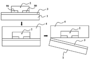
도 3은 본 개시에 따라 반도체 소자 구조물을 제조하는 방법의 일 예를 나타내는 도면으로서, 플레이트(1)를 준비한 다음, 두 개의 전극(80,90)이 구비된 반도체 소자(2)를 접착제(3)를 이용하여 플레이트(1)에 위치 고정한다. 다음으로, 봉지제(4; encapsulating material)를 이용하여, 반도체 소자(2)를 감싼다. 다음으로, 플레이트(1)와 반도체 소자(2)를 분리한다. 플레이트(1)를 이루는 물질에는 특별한 제한이 없으며, 사파이어와 같은 물질을 사용하여도 좋고, 금속이나 유리 등의 평평평한 구조물을 사용하여도 좋다. 접착제(3)를 이루는 물질에도 특별한 제한이 없으며, 반도체 소자(2)를 플레이트(1)에 위치 고정만 할 수 있다면 어떠한 접착제여도 좋다. 봉지제(3)를 이루는 물질로는 종래에 LED 패키지에 사용되는 실리콘 에폭시가 사용될 수 있다. 봉지제(4)가 형성된 후, 반도체 소자(2)와 플레이트(1)의 분리는 접착제(3)를 녹일 수 있는 열을 가하거나, 접착제(3)를 녹일 수 있는 용제를 이용함으로써 가능하다. 열과 용제를 함께 사용하는 것도 가능하다. 또한 접착 테이프를 이용하는 것도 가능하다. 봉지제(4)는 종래에 사용되는 디스펜싱, 스크린 프린팅, 몰딩, 스핀 코팅 등의 방법으로 형성할 수 있으며, 광경화성 수지(UV경화성 수지)를 도포한 후, 광을 조사함으로써 형성하는 것도 가능하다. 플레이트(1)로 사파이어와 같이 투광성 플레이트가 사용되는 경우에, 플레이트(1) 측으로부터 광을 조사하는 것도 가능하다. 설명을 위해, 플레이트(1) 위에 하나의 반도체 소자(2)를 도시하였지만, 복수의 반도체 소자(2)를 플레이트(1) 위에 두고 공정을 행할 수 있다. 여기서 반도체 소자(2)는 두 개의 전극(80,90)을 가지는 것으로 설명되었지만, 그 수에 특별히 제한이 있는 것은 아니다. 예를 들어, 트랜지스터의 경우에 세 개의 전극을 가질 수 있다.3 is a view illustrating an example of a method of manufacturing a semiconductor device structure according to the present disclosure. After the
도 4는 본 개시에 따라 플립 칩 패키지를 제조하는 방법의 일 예를 나타내는 도면으로서, 반도체 소자(2)로서, 정션 다운 형 칩이 제시되어 있다. 정션 다운 형 칩으로서, 도 2에 도시된 것과 같은 플립 칩형 반도체 발광소자를 예로 들 수 있다. 따라서 반도체 발광소자는 도 2에서와 같이, 기판(100; 예: 사파이어 기판), 기판(100) 위에, 제1 도전성을 가지는 제1 반도체층(300; 예: n형 GaN층), 전자와 정공의 재결합을 통해 빛을 생성하는 활성층(400; 예: InGaN/(In)GaN MQWs), 제1 도전성과 다른 제2 도전성을 가지는 제2 반도체층(500; 예: p형 GaN층)이 순차로 증착되어 있으며, 그 위에 기판(100) 측으로 빛을 반사시키기 위한 3층으로 된 전극막(901; 예: Ag 반사막), 전극막(902; 예: Ni 확산 방지막) 및 전극막(903; 예: Au 본딩층)이 형성되어 있고, 식각되어 노출된 제1 반도체층(300) 위에 본딩 패드로 기능하는 전극(800; 예: Cr/Ni/Au 적층 금속 패드)이 형성된 구조를 가질 수 있다. 반도체 소자(2)는 두 개의 전극(80,90)을 가지며, 전극(90)은 도 2의 전극(901,902,903)과 같은 구성을 가져도 좋고, DBR(Distributed Bragg Reflector)과 금속 반사막의 조합으로 이루어져도 좋다. 전극(80)과 전극(90)은 SiO2와 같은 절연막(5)에 의해 전기적으로 절연되어 있다. 이후의 과정은 동일하며, 봉지제(4; encapsulating material)를 이용하여, 반도체 소자(2)를 감싼다. 다음으로, 플레이트(1)와 접착제(3)로부터 반도체 소자(2)를 분리한다.4 is a view illustrating an example of a method of manufacturing a flip chip package according to the present disclosure, wherein a junction down chip is presented as the
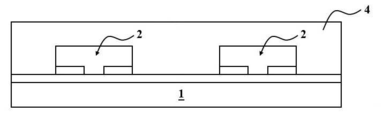
도 5는 본 개시에 따라 반도체 소자 구조물을 제조하는 방법의 다른 예를 나타내는 도면으로서, 플레이트(1) 위에 복수의 반도체 소자(2,2)가 일체로 봉지제(4)에 의해 덮혀 있다. 플레이트(1)를 제거한 후, 반도체 소자(2,2)를 일체로서 하나의 패키지화하는 것이 용이해진다. 반도체 소자(2)와 반도체 소자(2)의 전기적 연결 방법에 대해서는 후술한다. 또한 이들을 도 3에서와 같이 개별적인 반도체 소자(2)로 분리하는 것도 가능하다. 이는 복수의 반도체 소자(2,2)를 플레이트(1)로부터 분리한 후, 쏘잉(sawing) 등의 공정을 통해 개별화함으로써 가능하다. 경화후 연성을 가지는 봉지제(4)를 사용함으로써, 연성 회로기판과의 결합을 한층 높일 수 있게 된다.FIG. 5 shows another example of a method for manufacturing a semiconductor device structure according to the present disclosure, in which a plurality of
도 6은 본 개시에 따른 반도체 소자 구조물의 일 예를 나타내는 도면으로서, 봉지제(4)의 측면(4a)이 경사지도록 형성되어 있다. 반도체 소자(2)가 발광소자인 경우에, 봉지제(4)가 다양한 각의 외면을 갖게 되어, 패키지 외부로의 광 추출 효율이 높아지게 된다. 스크린 프린팅시, 스크린 격벽을 경사지게 형성하여 측면(4a)의 형성이 가능하며, 쏘잉시, 끝이 뾰족한 커터를 이용함으로써 측면(4a)의 형성이 가능하다.6 is a view illustrating an example of a semiconductor device structure according to the present disclosure, and is formed such that the
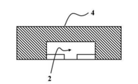
도 7은 본 개시에 따라 반도체 소자 구조물을 제조하는 방법의 또 다른 예를 나타내는 도면으로서, 플레이트(1)가 제거된 후, SiO2와 같은 절연막(6)을 전극(80)과 전극(90)을 노출한 상태로 구비하고 있다. 이후, 전극(80)에 외부 전극(81)을 연결하고, 전극(90)에 외부 전극(91)을 형성하여, 종래의 패키지와 같은 구조로 만들 수 있게 된다. 외부 전극(81,91)은 종래 패키지의 리드 프레임에 대응할 수 있다. 또한 외부 전극(81,91)을 반사막으로 기능하도록 넓게 펼쳐 증착하는 것도 가능하다. 절연막(6)은 단순히 절연 기능만을 하여도 좋고, 외부 전극(81,91)에 의한 광 흡수를 줄이도록 SiO2/TiO2의 교대 적층구조를 형성하거나 DBR을 이루어도 좋다. 도 4에서와 같이 반도체 소자(2)가 절연막(5)을 구비하는 경우에는 절연막(6)이 생략될 수도 있다. 절연막(6)과 외부 전극(81,91)의 형성에 사용되는 증착 공정과 포토리쏘그라피 공정 등은 반도체 칩 공정에서 일반적인 것으로 당업자에 매우 익숙한 것이다. 외부 전극(81,91)을 구비함으로써, PCB, COB 등에의 장착이 보다 용이해질 수 있다. 필요한 경우에, 외부 전극(81,91) 없이 절연막(6)만을 구비하는 것도 가능하다. 절연막(6) 반도체 소자(2)와 봉지제(4) 사이를 보호하는 기능을 할 뿐만 아니라, 봉지제(4)를 외부 전극(81,91) 형성 공정으로부터 보호하는 기능도 할 수 있다. 또한 절연막(6)을 백색 물질로 형성하여, 절연막(6)을 반사막으로 기능하게 할 수 있다. 예를 들어, 백색의 PSR(Photo Sloder Regist)을 절연막(6)으로 이용하거나, 코팅하여 사용할 수 있다. 예를 들어, 백색의 PSR을 스크린 프린팅 또는 스핀 코팅한 다음, 일반적인 포토리소그라피 공정을 통해 패터닝할 수 있다.FIG. 7 is a view showing another example of a method of manufacturing a semiconductor device structure according to the present disclosure. After the
도 8은 본 개시에 따른 반도체 소자 구조물의 다른 예를 나타내는 도면으로서, 전기적으로 직렬 연결된 반도체 소자(2A)와 반도체 소자(2B)가 구비되어 있다. 반도체 소자(2A)의 음(-) 전극(80A)과 반도체 소자(2B)의 양(+) 전극(90B)을 외부 전극(89)을 통해 연결함으로써 이러한 구성이 가능해진다. 미설명 부호 4는 봉지제이며, 6은 절연막이고, 90A은 반도체 소자(2A)의 양(+) 전극이며, 80B는 반도체 소자(2B)의 음(-) 전극이다. 이러한 구성을 통해, 모노리식 기판의 사용 없이, 봉지제(4)를 통해 일체화된 반도체 소자(2A,2B) 간의 전기적 연결을 형성할 수 있게 된다. 모노리식 기판의 경우에, 그 위의 반도체 소자의 구조가 동일하지만, 본 개시의 방법에 의하면, 반도체 소자(2A)와 반도체 소자(2B)가 같은 기능의 소자일 필요가 없다. 반도체 소자(2A,2B)를 병렬연결할 수 있음은 물론이다. 또한 봉지제(4)의 측면(4a)을 도 6에서와 같이 경사지게 형성할 수 있으며, 이러한 구성은 기존에 상상할 수 없었던 고전압(High-Voltage) 반도체 발광소자 패키지 내지는 반도체 발광소자 구조물을 가능하게 한다.8 is a diagram illustrating another example of a semiconductor device structure according to the present disclosure, and includes a
도 9는 본 개시에 따른 반도체 소자 구조물 사용의 일 예를 나타내는 도면으로서, 반도체 소자(2C)는 인쇄회로기판(7)의 도선(7a)과 전극(80,90)이 직접 연결되어 있으며, 반도체 소자(2D)는 도선(7b)과 외부 전극(81,91)을 통해 연결되어 있다. 인쇄회로기판(7)은 연성 회로기판이어도 좋다.9 is a view illustrating an example of the use of a semiconductor device structure according to the present disclosure. In the
도 10은 본 개시에 따라 반도체 소자 구조물을 제조하는 방법의 또 다른 예를 나타내는 도면으로서, 도 2에 도시된 것과 같은 반도체 소자(2)가 구비되어 있으며, 반도체 소자(2)는 기판(100), 기판(100) 위에, 제1 도전성을 가지는 제1 반도체층(300), 전자와 정공의 재결합을 통해 빛을 생성하는 활성층(400), 제1 도전성과 다른 제2 도전성을 가지는 제2 반도체층(500)이 성장되며, 전극(80,90)이 형성되어 있다. 반도체 소자(2)를 접착제(3)를 이용해 플레이트(1)에 붙인 다음, 봉지제(4)로 덮기에 앞서, 기판(100)을 제거하고, 바람직하게는 광 취출 효율을 높이기 위해 거친 표면(301)을 형성한다. 이후의 과정은 동일하다. 기판(100)의 제거는 레이저 리프트 오프(Laser Lift-off)와 같은 공정에 의해 가능하며, 거친 표면(301)은 ICP(Inductively Coupled Plasma)와 같은 건식 식각을 통해 가능하다. 이것은 칩 레벨 레이저 리프트 오프를 가능하게 한다.FIG. 10 is a view showing another example of a method of manufacturing a semiconductor device structure according to the present disclosure, in which a
도 11은 본 개시에 따른 반도체 소자 구조물의 또 다른 예를 나타내는 도면으로서, 봉지제(4)에 형광체가 포함되어 있다. YAG, Silicate, Nitride 형광체 등을 이용하여 원하는 색의 광을 발광할 수 있게 된다.FIG. 11 is a view showing another example of a semiconductor device structure according to the present disclosure, in which an
도 12은 본 개시에 따른 반도체 소자 구조물의 또 다른 예를 나타내는 도면으로서, 봉지제(4) 내에 또는 봉지제(4) 하부에 형광체층(8)이 형성되어 있다. 이는 봉지제(4) 내에서 형광체를 침전시키거나, 별도로 스핀 코팅하거나, 휘발성 액체에 담긴 형광체를 도포한 후 휘발시켜 형광체만 남긴 후 봉지제(4)로 덮음으로써 형성할 수 있다. 필요에 따라 복수의 형광체층(8)의 형성도 가능하다.12 illustrates another example of the semiconductor device structure according to the present disclosure, in which a
도 13은 본 개시에 따른 반도체 소자 구조물의 또 다른 예를 나타내는 도면으로서, 봉지제(4)에 광 취출 효율을 높이기 위한 거친 표면 또는 요철(4g)이 형성되어 있다. 거친 표면(4g)은 pressing, 나노임프린트(nanoimprint) 등의 성형을 통해 형성이 가능하다. 또한 bead 물질을 도포한 후, 에칭, 샌드블라스팅 등의 방법을 통해 형성하는 것도 가능하다. 거친 표면(4g)은 플레이트(1)의 분리 이전 또는 분리 이후에 형성될 수 있다.FIG. 13 is a view showing still another example of the semiconductor device structure according to the present disclosure, in which the
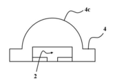
도 14는 본 개시에 따른 반도체 소자 구조물의 또 다른 예를 나타내는 도면으로서, 봉지제(4)에 렌즈(4c)가 형성되어 있다. 바람직하게는 렌즈(4c)는 봉지제와 일체로 형성된다. 이러한 일체형 렌즈(4c)는 압축성형 등으로 방법으로 형성하는 것이 가능하다.FIG. 14 is a view showing still another example of the semiconductor device structure according to the present disclosure, in which a
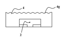
도 16은 본 개시에 따른 반도체 소자 구조물의 또 다른 예를 나타내는 도면으로서, 봉지제(4)의 상측에 거친 표면 또는 요철(4g)이 형성되어 있으며, 봉지제(4) 하측, 반도체 소자(2)의 전극(80,90)이 위치하는 측에도 봉지제(4)에 거친 표면 또는 요철(4h)이 형성되어 있다. 어느 일 측에만 요철(4g)이 형성될 수 있음은 물론이다.반도체 소자(2)가 반도체 발광소자인 경우에, 요철(4g)은 광을 산란시키는 산란면으로서 기능할 수 있다. 요철(4h)에 의해, 봉지제(4)와, 절연막(6) 및/또는 외부 전극(81,91)이 마주하는 면적이 확대되어, 이들 간의 결합력이 향상될 수 있다. 또 요철(4h)에 의해 측방으로의 움직임이 억제되어 결합력이 향상될 수 있다.FIG. 16 is a view showing still another example of the semiconductor device structure according to the present disclosure. A rough surface or
도 17은 도 16에 제시된 반도체 소자 구조물을 제조하는 방법의 일 예를 나타내는 도면으로서, 플레이트(1) 위에 반도체 소자(2)를 위치 고정한 상태에서, 가압 판(4j)을 이용해 봉지제(4)에 요철(4g; 도 16 참조)을 형성하는 과정을 나타내고 있다. FIG. 17 is a view illustrating an example of a method of manufacturing the semiconductor device structure illustrated in FIG. 16. In the state where the
도 18은 도 16에 제시된 반도체 소자 구조물을 제조하는 방법의 다른 예를 나타내는 도면으로서, 반도체 소자(2)에 절연막(6)과 외부 전극(81,91)을 형성한 다음, 가압 판(4k)을 이용해, 요철(4h; 도 16 참조)을 형성하는 과정을 나타내고 있다. 여기서 가압 판(4j)이 도 18에서와 같이 평탄일 수 있으며, 도 17에서와 같이 요철을 가질 수도 있다. 가압 판(4k)을 봉지제(4) 상측에 두고, 평탄한 또는 요철을 가진 가압 판(4j)을 봉지제(4) 하측에 둘 수 있음은 물론이다.FIG. 18 is a view showing another example of the method of manufacturing the semiconductor device structure shown in FIG. 16, wherein the insulating
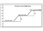
도 19는 도 16에 제시된 반도체 소자 구조물을 제조하는 과정에서 봉지제를 경화하는 공정의 일 예를 나타내는 도면이다. 봉지제(4)가 열 경화성 수지(예: 실리콘 에폭시 수지)인 경우에, 경화가 완료되면 요철(4g,4h)을 형성하는 것이 쉽지 않으므로, 경화가 완료되기 이전에 요철(4g,4h)을 형성하는 것이 바람직하다. 또한 요철(4g,4h)을 형성하는 과정에서 경화가 완료되도록 함으로써, 요철(4g,4h)이 가압 판(4j,4k)의 형상을 그대로 따르도록 할 수 있다. 예를 들어, 봉지제(4)를 유리전이온도(Glass Transition Temperatur) 이상에 둔 상태에서 요철(4g,4h)을 형성하는 것이 가능하다. 한번에 높은 온도에서 경화를 진행할 경우, 봉지제(4)에 물결모양 및 기포가 발생하여 깨끗한 면을 가질 수 없다. 이를 해결하기 위해, 스텝별로 온도를 서서히 올리면, 봉지제(4)가 깨끗한 면을 가지게 할 수 있다.FIG. 19 is a diagram illustrating an example of a process of curing an encapsulant in a process of manufacturing the semiconductor device structure illustrated in FIG. 16. In the case where the
이하 본 개시의 다양한 실시 형태에 대하여 설명한다.Various embodiments of the present disclosure will be described below.
(1) 봉지제가 캐리어로 역할하는 반도체 소자 구조물.(1) A semiconductor device structure in which an encapsulant serves as a carrier.
(2) 플레이트로부터 분리된 봉지제 하면을 가지는 반도체 소자 구조물.(2) A semiconductor device structure having a lower surface of the encapsulant separated from the plate.
(3) 반도체 소자의 전극이 위치하는 면을 제외한 봉지제의 외면들이 구조물 또는 패키지의 외면을 이루는 반도체 소자 구조물.(3) A semiconductor device structure in which the outer surfaces of the encapsulant except the surface where the electrodes of the semiconductor device are located form the outer surface of the structure or package.
(4) 반도체 소자들을 봉지제를 이용하여 결합한 반도체 소자 구조물.(4) A semiconductor device structure in which semiconductor devices are bonded using an encapsulant.
(5) 반도체 소자 구조물을 제조하는 방법에 있어서, 플레이트 위에 반도체 소자를 위치 고정하는 단계;로서, 반도체 소자의 전극이 플레이트를 향하도록 위치 고정하는 단계; 반도체 소자를 봉지제로 덮는 단계; 그리고, 봉지제가 덮힌 반도체 소자를 플레이트로부터 분리하는 단계;를 포함하는 것을 특징으로 하는 반도체 소자 구조물을 제조하는 방법.(5) A method of fabricating a semiconductor device structure, comprising: positioning a semiconductor device on a plate, the method comprising: positioning the electrode of the semiconductor device to face the plate; Covering the semiconductor element with an encapsulant; And separating the semiconductor device covered with the encapsulant from the plate.
(6) 반도체 소자 구조물을 제조하는 방법에 있어서, 플레이트 위에 반도체 소자를 위치 고정하는 단계;로서, 반도체 소자의 전극이 플레이트를 향하도록 위치 고정하는 단계; 반도체 소자를 봉지제로 덮는 단계; 봉지제가 덮힌 반도체 소자를 플레이트로부터 분리하는 단계; 그리고, 반도체 소자의 전극이 위치하는 측 및 봉지제의 상측 중의 적어도 일 측을 가압하여 요철을 형성하는 단계;를 포함하는 것을 특징으로 하는 반도체 소자 구조물을 제조하는 방법.(6) A method of manufacturing a semiconductor device structure, comprising the steps of: positioning a semiconductor device on a plate; positioning the electrode of the semiconductor device so as to face the plate; Covering the semiconductor element with an encapsulant; Separating the semiconductor device covered with the encapsulant from the plate; And pressing at least one of the side where the electrode of the semiconductor element is located and the upper side of the encapsulant to form the unevenness.
(7) 요철을 형성하는 단계에서, 적어도 봉지제의 상측에 산란면으로서 요철이 형성되며, 반소체 소자는 반도체 발광소자인 것을 특징으로 하는 반도체 소자 구조물을 제조하는 방법.(7) In the step of forming the unevenness, unevenness is formed as a scattering surface at least on the upper side of the encapsulant, and the semi-elementary element is a semiconductor light emitting device, characterized in that the manufacturing method of the semiconductor device structure.
(8) 요철을 형성하는 단계에서, 봉지제의 경화가 완료되는 것을 특징으로 하는 반도체 소자 구조물을 제조하는 방법.(8) A method of manufacturing a semiconductor device structure, wherein in the step of forming the unevenness, curing of the encapsulant is completed.
(9) 요철을 형성하는 단계에 앞서, 전극을 노출하는 절연막을 형성하는 단계;를 더 포함하는 것을 특징으로 하는 반도체 소자 구조물을 제조하는 방법. 절연막만 형성될 수 있으며, 절연막을 형성한 다음 외부 전극이 형성될 수 있고, 외부 전극을 형성한 다음 절연막을 형성할 수도 있다.(9) prior to forming the unevenness, forming an insulating film exposing the electrode; the method of manufacturing a semiconductor device structure, characterized in that it further comprises. Only an insulating film may be formed, and after forming the insulating film, an external electrode may be formed, or after forming the external electrode, an insulating film may be formed.
(10) 요철을 형성하는 단계에 앞서, 전극과 전기적으로 연결되는 외부 전극을 형성하는 단계;를 더 포함하는 것을 특징으로 하는 반도체 소자 구조물을 제조하는 방법.(10) prior to forming the unevenness, forming an external electrode electrically connected with the electrode; the method of manufacturing a semiconductor device structure, characterized in that it further comprises.
(11) 요철을 형성하는 단계를 통해, 봉지제와 외부 전극이 마주하는 면적이 확대되는 것을 특징으로 하는 반도체 소자 구조물을 제조하는 방법. 양자의 결합 면적이 넓어져, 양자의 결합력이 향상될 수 있으며, 요철을 형성의 과정에서 열을 가하여, 양자의 결합력을 높일 수도 있다.(11) A method of manufacturing a semiconductor device structure, characterized in that by forming the unevenness, the area facing the encapsulant and the external electrode is enlarged. The bonding area of the protons is widened, and thus the bonding force of the protons can be improved, and the bonding force of the protons can be increased by applying heat in the process of forming the unevenness.
(12) 요철을 형성하는 단계를 통해, 봉지제와, 절연막 및 외부 전극이 마주하는 면적이 확대되는 것을 특징으로 하는 반도체 소자 구조물을 제조하는 방법.(12) A method of manufacturing a semiconductor device structure comprising the step of forming an unevenness, the area of the encapsulant, the insulating film and the external electrode facing each other is expanded.
본 개시에 따른 하나의 반도체 소자 구조물을 제조하는 방법에 의하면, 반도체 소자 구조물 또는 패키지를 쉽게 제조할 수 있게 된다.The method of manufacturing a semiconductor device structure according to the present disclosure makes it possible to easily manufacture a semiconductor device structure or a package.
또한 본 개시에 따른 다른 반도체 소자 구조물을 제조하는 방법에 의하면, 봉지제가 캐리어로 역할하는 구조물 또는 패키지를 만들 수 있게 된다.In addition, according to the method of manufacturing another semiconductor device structure according to the present disclosure, it is possible to make a structure or package in which the encapsulant serves as a carrier.
또한 본 개시에 따른 또 다른 반도체 소자 구조물을 제조하는 방법에 의하면, 투광성 봉지제가 캐리어로 역할하는 발광소자 구조물 또는 패키지를 만들 수 있게 된다.Further, according to another method of manufacturing a semiconductor device structure according to the present disclosure, a light emitting device structure or a package in which a transparent encapsulant serves as a carrier can be manufactured.
또한 본 개시에 따른 또 다른 반도체 소자 구조물을 제조하는 방법에 의하면, 복수의 반도체 소자를 쉽게 전기적으로 연결할 수 있게 된다.Further, according to another method of manufacturing a semiconductor device structure according to the present disclosure, a plurality of semiconductor devices can be easily electrically connected.
또한 본 개시에 따른 또 다른 반도체 소자 구조물을 제조하는 방법에 의하면, 다른 구조의 반도체 소자들을 쉽게 전기적으로 연결할 수 있게 된다.In addition, according to the method of manufacturing another semiconductor device structure according to the present disclosure, semiconductor devices of different structures can be easily electrically connected.
또한 본 개시에 따른 또 다른 반도체 소자 구조물을 제조하는 방법에 의하면, 봉지제에 거친 표면 또는 요철을 쉽게 형성할 수 있게 된다.In addition, according to the method of manufacturing another semiconductor device structure according to the present disclosure, it is possible to easily form a rough surface or irregularities in the encapsulant.
또한 본 개시에 따른 또 다른 반도체 소자 구조물을 제조하는 방법에 의하면, 요철을 형성하여, 봉지제와, 절연막 및/또는 외부 전극 간의 결합력을 향상시킬 수 있게 된다.In addition, according to the method of manufacturing another semiconductor device structure according to the present disclosure, it is possible to form irregularities, thereby improving the bonding force between the sealing agent and the insulating film and / or the external electrode.
100: 기판 200: 버퍼층 300,400,500: 반도체층100: substrate 200:
Claims (10)
플레이트 위에 반도체 소자를 위치 고정하는 단계;로서, 반도체 소자의 전극이 플레이트를 향하도록 위치 고정하는 단계;
반도체 소자를 봉지제로 덮는 단계;
봉지제가 덮힌 반도체 소자를 플레이트로부터 분리하는 단계; 그리고,
반도체 소자의 전극이 위치하는 측 및 봉지제의 상측 중의 적어도 일 측을 가압하여 요철을 형성하는 단계;를 포함하는 것을 특징으로 하는 반도체 소자 구조물을 제조하는 방법.In the method of manufacturing a semiconductor device structure,
Positioning the semiconductor element on the plate, the method comprising: positioning the electrode of the semiconductor element toward the plate;
Covering the semiconductor element with an encapsulating material;
Separating the encapsulant-covered semiconductor element from the plate; And,
And pressing at least one of the side where the electrode of the semiconductor element is located and the upper side of the encapsulant to form the unevenness.
요철을 형성하는 단계에서, 적어도 봉지제의 상측에 산란면으로서 요철이 형성되며,
반소체 소자는 반도체 발광소자인 것을 특징으로 하는 반도체 소자 구조물을 제조하는 방법.The method according to claim 1,
In the step of forming the irregularities, irregularities are formed as a scattering surface at least on the upper side of the encapsulant,
A semi-elementary device is a method of manufacturing a semiconductor device structure, characterized in that the semiconductor light emitting device.
요철을 형성하는 단계에서, 봉지제의 경화가 완료되는 것을 특징으로 하는 반도체 소자 구조물을 제조하는 방법.The method according to claim 1,
In the step of forming the irregularities, the method of manufacturing a semiconductor device structure, characterized in that the curing of the sealing agent is completed.
요철을 형성하는 단계에 앞서, 전극을 노출하는 절연막을 형성하는 단계;를 더 포함하는 것을 특징으로 하는 반도체 소자 구조물을 제조하는 방법.The method according to claim 1,
A method of manufacturing a semiconductor device structure, further comprising: forming an insulating film exposing the electrode prior to forming the unevenness.
요철을 형성하는 단계에 앞서, 전극과 전기적으로 연결되는 외부 전극을 형성하는 단계;를 더 포함하는 것을 특징으로 하는 반도체 소자 구조물을 제조하는 방법.The method according to claim 1,
Prior to forming the irregularities, forming an external electrode electrically connected to the electrode; method for manufacturing a semiconductor device structure, characterized in that it further comprises.
요철을 형성하는 단계에 앞서, 전극을 노출하는 절연막을 형성하는 단계; 및 절연막을 통해 노출된 전극과 전기적으로 연결되는 외부 전극을 형성하는 단계;를 더 포함하는 것을 특징으로 하는 반도체 소자 구조물을 제조하는 방법.The method according to claim 1,
Prior to forming the unevenness, forming an insulating film exposing the electrode; And forming an external electrode electrically connected to the exposed electrode through the insulating film.
요철을 형성하는 단계를 통해, 봉지제와 외부 전극이 마주하는 면적이 확대되는 것을 특징으로 하는 반도체 소자 구조물을 제조하는 방법.The method of claim 5,
A method of manufacturing a semiconductor device structure, characterized in that by forming an unevenness, the area facing the encapsulant and the external electrode is enlarged.
요철을 형성하는 단계를 통해, 봉지제와, 절연막 및 외부 전극이 마주하는 면적이 확대되는 것을 특징으로 하는 반도체 소자 구조물을 제조하는 방법.The method of claim 6,
A method of manufacturing a semiconductor device structure comprising the step of forming an unevenness, the area facing the encapsulant, the insulating film and the external electrode is enlarged.
요철을 형성하는 단계에서, 봉지제의 상측에 산란면으로서 요철이 형성되며,
반소체 소자는 반도체 발광소자인 것을 특징으로 하는 반도체 소자 구조물을 제조하는 방법.The method according to claim 8,
In the step of forming the irregularities, irregularities are formed as a scattering surface on the upper side of the encapsulant,
A semi-elementary device is a method of manufacturing a semiconductor device structure, characterized in that the semiconductor light emitting device.
요철을 형성하는 단계에서, 봉지제의 경화가 완료되는 것을 특징으로 하는 반도체 소자 구조물을 제조하는 방법.The method of claim 9,
In the step of forming the irregularities, the method of manufacturing a semiconductor device structure, characterized in that the curing of the sealing agent is completed.
Priority Applications (1)
| Application Number | Priority Date | Filing Date | Title |
|---|---|---|---|
| KR1020140037948A KR20140048178A (en) | 2014-03-31 | 2014-03-31 | Method of manufacutruing semiconductor device structure |
Applications Claiming Priority (1)
| Application Number | Priority Date | Filing Date | Title |
|---|---|---|---|
| KR1020140037948A KR20140048178A (en) | 2014-03-31 | 2014-03-31 | Method of manufacutruing semiconductor device structure |
Related Parent Applications (1)
| Application Number | Title | Priority Date | Filing Date |
|---|---|---|---|
| KR1020120093193A Division KR20140026154A (en) | 2012-04-06 | 2012-08-24 | Method of manufacutruing semiconductor device structure |
Publications (1)
| Publication Number | Publication Date |
|---|---|
| KR20140048178A true KR20140048178A (en) | 2014-04-23 |
Family
ID=50654368
Family Applications (1)
| Application Number | Title | Priority Date | Filing Date |
|---|---|---|---|
| KR1020140037948A KR20140048178A (en) | 2014-03-31 | 2014-03-31 | Method of manufacutruing semiconductor device structure |
Country Status (1)
| Country | Link |
|---|---|
| KR (1) | KR20140048178A (en) |
Cited By (1)
| Publication number | Priority date | Publication date | Assignee | Title |
|---|---|---|---|---|
| US11038086B2 (en) | 2016-03-07 | 2021-06-15 | Semicon Light Co., Ltd. | Semiconductor light-emitting element and manufacturing method therefor |
-
2014
- 2014-03-31 KR KR1020140037948A patent/KR20140048178A/en not_active Application Discontinuation
Cited By (1)
| Publication number | Priority date | Publication date | Assignee | Title |
|---|---|---|---|---|
| US11038086B2 (en) | 2016-03-07 | 2021-06-15 | Semicon Light Co., Ltd. | Semiconductor light-emitting element and manufacturing method therefor |
Similar Documents
| Publication | Publication Date | Title |
|---|---|---|
| TWI407591B (en) | White-light light emitting diode chips and fabrication methods thereof | |
| KR101476771B1 (en) | Semiconductor device structure and method of manufacutruing the same | |
| WO2013151387A1 (en) | Method for manufacturing semiconductor device structure | |
| KR20150107086A (en) | Semiconductor device structure and method of manufacutruing the same | |
| US8138509B2 (en) | Light emitting device having luminescent layer with opening to exposed bond pad on light emitting die for wire bonding pad to substrate | |
| US9831379B2 (en) | Method of manufacturing light emitting device | |
| KR101291092B1 (en) | Method of manufacutruing semiconductor device structure | |
| KR101461154B1 (en) | Method of manufacutruing semiconductor device structure | |
| KR101360324B1 (en) | Method of manufacutruing semiconductor device structure | |
| KR101460742B1 (en) | Method of manufacutruing semiconductor device structure | |
| KR101273481B1 (en) | White Light-emitting diode and Method of Manufacturing the same | |
| KR101300463B1 (en) | Method of manufacutruing semiconductor device structure | |
| KR101450216B1 (en) | Method of manufacutruing semiconductor device structure | |
| KR20140048178A (en) | Method of manufacutruing semiconductor device structure | |
| KR101299563B1 (en) | Method of manufacutruing semiconductor device structure | |
| KR101863538B1 (en) | Semiconductor Light Emitting Device And Method of Manufacturing the same | |
| KR102089496B1 (en) | Semiconductor light emitting structure and method ofmanufacturing the same | |
| KR101465708B1 (en) | Method of manufacturing a semiconductor device structure | |
| KR101299562B1 (en) | Semiconductor device structure | |
| KR101461153B1 (en) | Method of manufacutruing semiconductor device structure | |
| KR101779084B1 (en) | Semicondutor light emitting device structure and method of manufacturing the same | |
| KR20140026154A (en) | Method of manufacutruing semiconductor device structure | |
| KR101494440B1 (en) | Method of manufacutruing semiconductor device structure and semiconductor device structure using the method | |
| KR20130114011A (en) | Method of manufacutruing semiconductor device structure | |
| KR101543724B1 (en) | Semiconductor light emitting device and method of manufacturing the same |
Legal Events
| Date | Code | Title | Description |
|---|---|---|---|
| A107 | Divisional application of patent | ||
| WITN | Withdrawal due to no request for examination |