KR20140028362A - Semiconductor memory device - Google Patents
Semiconductor memory device Download PDFInfo
- Publication number
- KR20140028362A KR20140028362A KR1020120094440A KR20120094440A KR20140028362A KR 20140028362 A KR20140028362 A KR 20140028362A KR 1020120094440 A KR1020120094440 A KR 1020120094440A KR 20120094440 A KR20120094440 A KR 20120094440A KR 20140028362 A KR20140028362 A KR 20140028362A
- Authority
- KR
- South Korea
- Prior art keywords
- signal
- delay
- column
- unit
- response
- Prior art date
- Legal status (The legal status is an assumption and is not a legal conclusion. Google has not performed a legal analysis and makes no representation as to the accuracy of the status listed.)
- Granted
Links
Images


Classifications
-
- G—PHYSICS
- G11—INFORMATION STORAGE
- G11C—STATIC STORES
- G11C7/00—Arrangements for writing information into, or reading information out from, a digital store
- G11C7/22—Read-write [R-W] timing or clocking circuits; Read-write [R-W] control signal generators or management
-
- G—PHYSICS
- G11—INFORMATION STORAGE
- G11C—STATIC STORES
- G11C11/00—Digital stores characterised by the use of particular electric or magnetic storage elements; Storage elements therefor
- G11C11/21—Digital stores characterised by the use of particular electric or magnetic storage elements; Storage elements therefor using electric elements
- G11C11/34—Digital stores characterised by the use of particular electric or magnetic storage elements; Storage elements therefor using electric elements using semiconductor devices
- G11C11/40—Digital stores characterised by the use of particular electric or magnetic storage elements; Storage elements therefor using electric elements using semiconductor devices using transistors
- G11C11/401—Digital stores characterised by the use of particular electric or magnetic storage elements; Storage elements therefor using electric elements using semiconductor devices using transistors forming cells needing refreshing or charge regeneration, i.e. dynamic cells
- G11C11/4063—Auxiliary circuits, e.g. for addressing, decoding, driving, writing, sensing or timing
- G11C11/407—Auxiliary circuits, e.g. for addressing, decoding, driving, writing, sensing or timing for memory cells of the field-effect type
- G11C11/4076—Timing circuits
-
- G—PHYSICS
- G11—INFORMATION STORAGE
- G11C—STATIC STORES
- G11C11/00—Digital stores characterised by the use of particular electric or magnetic storage elements; Storage elements therefor
- G11C11/21—Digital stores characterised by the use of particular electric or magnetic storage elements; Storage elements therefor using electric elements
- G11C11/34—Digital stores characterised by the use of particular electric or magnetic storage elements; Storage elements therefor using electric elements using semiconductor devices
- G11C11/40—Digital stores characterised by the use of particular electric or magnetic storage elements; Storage elements therefor using electric elements using semiconductor devices using transistors
- G11C11/401—Digital stores characterised by the use of particular electric or magnetic storage elements; Storage elements therefor using electric elements using semiconductor devices using transistors forming cells needing refreshing or charge regeneration, i.e. dynamic cells
- G11C11/4063—Auxiliary circuits, e.g. for addressing, decoding, driving, writing, sensing or timing
- G11C11/407—Auxiliary circuits, e.g. for addressing, decoding, driving, writing, sensing or timing for memory cells of the field-effect type
- G11C11/409—Read-write [R-W] circuits
- G11C11/4097—Bit-line organisation, e.g. bit-line layout, folded bit lines
-
- G—PHYSICS
- G11—INFORMATION STORAGE
- G11C—STATIC STORES
- G11C7/00—Arrangements for writing information into, or reading information out from, a digital store
- G11C7/06—Sense amplifiers; Associated circuits, e.g. timing or triggering circuits
-
- G—PHYSICS
- G11—INFORMATION STORAGE
- G11C—STATIC STORES
- G11C7/00—Arrangements for writing information into, or reading information out from, a digital store
- G11C7/10—Input/output [I/O] data interface arrangements, e.g. I/O data control circuits, I/O data buffers
-
- G—PHYSICS
- G11—INFORMATION STORAGE
- G11C—STATIC STORES
- G11C7/00—Arrangements for writing information into, or reading information out from, a digital store
- G11C7/10—Input/output [I/O] data interface arrangements, e.g. I/O data control circuits, I/O data buffers
- G11C7/1078—Data input circuits, e.g. write amplifiers, data input buffers, data input registers, data input level conversion circuits
- G11C7/1087—Data input latches
-
- G—PHYSICS
- G11—INFORMATION STORAGE
- G11C—STATIC STORES
- G11C7/00—Arrangements for writing information into, or reading information out from, a digital store
- G11C7/12—Bit line control circuits, e.g. drivers, boosters, pull-up circuits, pull-down circuits, precharging circuits, equalising circuits, for bit lines
-
- G—PHYSICS
- G11—INFORMATION STORAGE
- G11C—STATIC STORES
- G11C7/00—Arrangements for writing information into, or reading information out from, a digital store
- G11C7/22—Read-write [R-W] timing or clocking circuits; Read-write [R-W] control signal generators or management
- G11C7/227—Timing of memory operations based on dummy memory elements or replica circuits
-
- G—PHYSICS
- G11—INFORMATION STORAGE
- G11C—STATIC STORES
- G11C8/00—Arrangements for selecting an address in a digital store
- G11C8/10—Decoders
-
- G—PHYSICS
- G11—INFORMATION STORAGE
- G11C—STATIC STORES
- G11C2207/00—Indexing scheme relating to arrangements for writing information into, or reading information out from, a digital store
- G11C2207/005—Transfer gates, i.e. gates coupling the sense amplifier output to data lines, I/O lines or global bit lines
-
- G—PHYSICS
- G11—INFORMATION STORAGE
- G11C—STATIC STORES
- G11C2207/00—Indexing scheme relating to arrangements for writing information into, or reading information out from, a digital store
- G11C2207/22—Control and timing of internal memory operations
- G11C2207/229—Timing of a write operation
Landscapes
- Engineering & Computer Science (AREA)
- Microelectronics & Electronic Packaging (AREA)
- Computer Hardware Design (AREA)
- Dram (AREA)
Abstract
컬럼 선택신호를 이용하는 반도체 메모리 장치에 관한 것으로, 라이트 인에이블신호를 복수의 메모리 영역의 배치 위치에 대응하는 지연시간만큼 지연시켜 제1 지연신호를 생성하기 위한 제1 레플리카 지연부; 제1 지연신호를 지연시간만큼 지연시켜 제2 지연신호를 생성하기 위한 제2 레플리카 지연부; 라이트 인에이블신호와 제1 및 제2 지연신호에 응답하여 라이트 인에이블신호보다 지연시간만큼 지연된 제1 컬럼 소오스신호를 생성하기 위한 컬럼 소오스신호 생성부; 및 제1 컬럼 소오스신호에 응답하여 라이트용 컬럼 선택신호를 생성하기 위한 컬럼 디코더를 포함하는 반도체 메모리 장치가 제공된다.A semiconductor memory device using a column selection signal, comprising: a first replica delay unit configured to delay a write enable signal by a delay time corresponding to an arrangement position of a plurality of memory regions to generate a first delay signal; A second replica delay unit configured to delay the first delay signal by a delay time to generate a second delay signal; A column source signal generator configured to generate a first column source signal delayed by a delay time from the write enable signal in response to the write enable signal and the first and second delay signals; And a column decoder for generating a column selection signal for writing in response to the first column source signal.
Description
본 발명은 반도체 설계 기술에 관한 것으로, 더욱 상세하게는 반도체 메모리 장치에 관한 것이다.
BACKGROUND OF THE
일반적으로, 디램(DRAM : Dynamic Random Access Memory)과 같은 반도체 메모리 장치는 데이터를 저장하는 라이트 동작과 저장된 데이터를 독출하는 리드 동작을 수행한다. 여기서, 라이트 동작시에는 액티브(Active) 신호에 의해 해당 워드 라인(Word Line : WL)을 인에이블시킨 상태에서, 라이트 드라이버(Write Driver)를 통해 글로벌 입출력 라인(Global Input/Output Line : GIO)에 실린 데이터를 로컬 데이터 라인(Local Input/Output Line : LIO)에 전달하고, 로컬 데이터 라인(LIO)에 실린 데이터를 컬럼 선택신호에 따라 선택된 비트 라인 감지 증폭기(Bit Line Sense Amplifier : BLSA)로 전달함으로써 해당 메모리 셀(Cell)에 저장한다. 반대로, 리드 동작시에는 액티브 신호에 의해 해당 워드 라인(WL)을 인에이블시킨 상태에서, 해당 메모리 셀에 저장된 데이터를 비트 라인(Bit Line : BL)을 통해 비트 라인 감지 증폭기(BLSA)에서 증폭시킨 다음, 증폭된 데이터를 컬럼 선택신호에 따라 로컬 데이터 라인(LIO)으로 전달하고, 입출력 감지 증폭기(Input/Output Sense Amplifier : IOSA)에서 증폭되어 글로벌 데이터 라인(GIO)으로 전달된다. 상기와 같이 로컬 입출력 라인(LIO)과 비트 라인 감지 증폭기(BLSA) 사이에서 데이터를 전송시키기 위해서는 해당 비트 라인(BL)을 선택하기 위한 컬럼 선택신호가 이용되며, 컬럼 선택신호에 의하여 액세스(access) 타이밍이 결정된다.In general, a semiconductor memory device such as a dynamic random access memory (DRAM) performs a write operation for storing data and a read operation for reading the stored data. Here, in the write operation, the word line WL is enabled by an active signal, and a write driver is applied to a global input / output line (GIO) through a write driver. By passing the carried data to a local data line (Local Input / Output Line (LIO)) and passing the data carried on the local data line (LIO) to a bit line sense amplifier (BLSA) selected according to a column selection signal. It is stored in the corresponding memory cell. On the contrary, in the read operation, while the word line WL is enabled by the active signal, the data stored in the memory cell is amplified by the bit line sense amplifier BLSA through the bit line BL. Next, the amplified data is transferred to the local data line (LIO) according to the column selection signal, amplified by an input / output sense amplifier (IOSA), and transferred to the global data line (GIO). As described above, in order to transfer data between the local input / output line LIO and the bit line sense amplifier BLSA, a column select signal for selecting the corresponding bit line BL is used, and is accessed by the column select signal. The timing is determined.
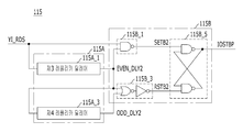
도 1에는 종래기술에 따른 반도체 메모리 장치의 컬럼 선택신호 생성회로가 구성도로 도시되어 있다.1 is a block diagram of a column selection signal generation circuit of a semiconductor memory device according to the prior art.
도 1을 참조하면, 컬럼 선택신호 생성회로(10)는 인버터 체인으로 구성되며, 소오스신호(BCS)에 응답하여 각각의 지연시간 이후에 예정된 신호(BWEN, YI_S, IOSTBP)를 생성한다. 여기서, 소오스신호(BCS)는 라이트 명령 및 리드 명령시에 각각의 예정된 레이턴시 이후에 활성화되는 신호이다.Referring to FIG. 1, the column select
한편, 컬럼 선택신호 생성회로(10)는 라이트 모드시 소오스신호(BCS)에 응답하여 예정된 지연시간 이후에 라이트 인에이블신호(BWEN)를 생성하고, 라이트 인에이블신호(BWEN)를 제1 지연시간만큼 지연시켜 컬럼 소오스신호(YI_S)를 생성한다. 여기서, 라이트 인에이블신호(BWEN)는, 라이트 드라이버(도면에 미도시)에 입력되는 신호로, 라이트 드라이버가 라이트 인에이블신호(BWEN)에 따라 글로벌 입출력 라인(GIO)에 실린 데이터를 로컬 입출력 라인(LIO)으로 전달하게 된다. 그리고, 컬럼 소오스신호(YI_S)는, 컬럼 디코더(도면에 미도시)에 입력되는 신호로, 컬럼 디코더가 컬럼 소오스신호(YI_S)에 따라 컬럼 선택신호(도면에 미도시)를 생성하므로, 이하에서는 설명의 편의를 위해 컬럼 소오스신호(YI_S)를 컬럼 선택신호라 칭하여 설명하기로 한다.Meanwhile, the column select
그리고, 컬럼 선택신호 생성회로(10)는 리드 모드시 소오스신호(BCS)에 응답하여 예정된 지연시간 이후에 컬럼 선택신호(YI_S)를 생성하고, 컬럼 선택신호(YI_S)를 제2 지연시간만큼 지연시켜 리드 인에이블신호(IOSTBP)를 생성한다. 여기서, 리드 인에이블신호(IOSTBP)는, 입출력 감지 증폭기(IOSA)(도면에 미도시)에 입력되는 신호로, 입출력 감지 증폭기(IOSA)가 리드 인에이블신호(IOSTBP)에 따라 로컬 입출력 라인(LIO)에 실린 데이터를 글로벌 입출력 라인(GIO)으로 전달하게 된다.The column select
이하, 상기와 같은 구성을 가지는 컬럼 선택신호 생성회로(10)의 동작을 도 2a 및 도 2b를 참조하여 설명한다.Hereinafter, the operation of the column select
도 2a에는 라이트 모드시 컬럼 선택신호 생성회로(10)의 동작을 설명하기 위한 타이밍도가 도시되어 있고, 도 2b에는 리드 모드시 컬럼 선택신호 생성회로(10)의 동작을 설명하기 위한 타이밍도가 도시되어 있다.2A is a timing diagram illustrating the operation of the column select
도 2a를 참조하면, 라이트 커맨드(도면에 미도시)가 인가되고 예정된 레이턴시 이후에 소오스신호(BCS)가 생성된다. 그러면, 컬럼 선택신호 생성회로(10)는 소오스신호(BCS)에 응답하여 예정된 지연시간 이후에 라이트 인에이블신호(BWEN)를 생성하고, 라이트 인에이블신호(BWEN)를 제1 지연시간(D1)만큼 지연시켜 컬럼 선택신호(YI_S)를 생성한다.Referring to FIG. 2A, a write command (not shown) is applied and a source signal BCS is generated after a predetermined latency. Then, the column select
도 2b를 참조하면, 리드 커맨드(도면에 미도시)가 인가되고 예정된 레이턴시 이후에 소오스신호(BCS)가 생성된다. 그러면, 컬럼 선택신호 생성회로(10)는 소오스신호(BCS)에 응답하여 예정된 지연시간 이후에 컬럼 선택신호(YI_S)를 생성하고, 컬럼 선택신호(YI_S)를 제2 지연시간(D2)만큼 지연시켜 리드 인에이블신호(IOSTBP)를 생성한다.Referring to FIG. 2B, a read command (not shown) is applied and a source signal BCS is generated after a predetermined latency. Then, the column select
이와 같은 종래기술에 따른 컬럼 선택신호 생성회로(10)는 컬럼 경로를 순차적으로 제어하여 유효한(valid) 데이터를 라이트 및 리드할 수 있다.The column selection
그러나, 상기와 같은 구성을 가지는 컬럼 선택신호 생성회로(10)는 다음과 같은 문제점이 있다.However, the column selection
먼저, 컬럼 선택신호 생성회로(10)로부터 생성되는 컬럼 선택신호(YI_S)는 메모리 영역의 배치 위치에 따른 지연 보정이 고려되어 있지 못하다. 예컨대, 메모리 영역이 복수의 매트를 포함한다고 가정하면, 라이트 드라이버로부터 멀리 배치된 매트일수록 로컬 입출력 라인(LIO)을 통해 전송되는 데이터의 구동력은 감소한다. 이는 라이트 드라이버로부터 멀리 배치된 매트일수록 로컬 입출력 라인(LIO)에 반영되는 지연요소(또는 라인 로딩)가 커지기 때문이다. 따라서, 라이트 드라이버로부터 멀리 배치된 매트일수록 라이트되는 데이터가 지연되지만, 컬럼 선택신호(YI_S)는 복수의 매트의 배치 위치에 상관없이 일정한 지연시간(D1)이 반영된 컬럼 선택신호(YI_S)를 생성하고 있다. 이러한 경우, 컬럼 선택신호(YI_S)는 메모리 영역의 배치 위치에 따라 라이트 데이터가 전송되는 시점보다 상대적으로 늦게 생성되거나 또는 빠르게 생성되는 결과를 초래하므로, 라이트 리커버리 타임(tWR)이 손실되고 무효한(invalid) 데이터가 라이트되는 문제점이 있다.First, in the column select signal YI_S generated from the column select
한편, 상기와 같은 이유로 인하여 리드 인에이블신호(IOSTBP) 또한 상대적으로 늦게 생성되거나 또는 빠르게 생성되는 결과를 초래하며, 이러한 경우 어드레스 액세스 타임(tAA)이 손실되고 무효한 데이터가 리드되는 문제점이 있다.On the other hand, the read enable signal IOSTBP is also generated relatively late or quickly due to the above reason. In this case, the address access time tAA is lost and invalid data is read.
다음으로, 인버터 체인은 통상적으로 트랜지스터를 포함하여 구성되기 때문에 프로세스·전압·온도(PVT) 변동에 민감하다. 예컨대, 높은 전원전압(high VDD) 환경에서는 인버터 체인을 통한 지연시간이 감소하고, 낮은 전원전압(Low VDD) 환경에서는 인버터 체인을 통한 지연시간이 증가하기 때문에, 전압 변동에 따른 지연량 변화로 인하여 컬럼 선택신호(YI_S)가 원하는 타이밍에 정상적으로 생성되지 못한다. 따라서, 프로세스·전압·온도(PVT) 변동으로 인하여 무효한(invalid) 데이터가 라이트 및 리드되는 문제점이 있다.
Next, since the inverter chain usually includes transistors, it is sensitive to process, voltage, and temperature (PVT) variations. For example, in the high VDD environment, the delay time through the inverter chain decreases, and in the low VDD environment, the delay time through the inverter chain increases. The column select signal YI_S is not normally generated at a desired timing. Therefore, there is a problem that invalid data is written and read due to process, voltage, and temperature (PVT) variations.
본 발명은 복수의 메모리 영역의 배치 위치가 고려된 컬럼 선택신호를 생성하기 위한 반도체 장치를 제공하는 것이다.SUMMARY OF THE INVENTION The present invention provides a semiconductor device for generating a column select signal in which arrangement positions of a plurality of memory regions are considered.
또한, 본 발명은 복수의 메모리 영역의 배치 위치가 고려된 컬럼 선택신호를 생성하면서도 프로세스·전압·온도(PVT) 변동에 둔감한 반도체 장치를 제공하는 것이다.
In addition, the present invention provides a semiconductor device which is insensitive to process, voltage, and temperature (PVT) variations while generating a column selection signal considering the arrangement positions of a plurality of memory regions.
본 발명의 일 측면에 따르면, 본 발명은 복수의 지연시간 중에서 데이터가 입출력되는 메모리 영역의 배치 위치에 따라 선택된 지연시간이 서로 다른 배수로 반영된 제1 및 제2 지연신호를 제1 컬럼 제어신호에 응답하여 순차적으로 생성하기 위한 제1 신호 생성부; 및 제1 컬럼 제어신호보다 지연시간만큼 지연된 제2 컬럼 제어신호를 생성하되, 제1 지연신호에 응답하여 제2 컬럼 제어신호의 활성화 시점을 결정하고 제2 지연신호에 응답하여 제2 컬럼 제어신호의 비활성화 시점을 결정하는 제2 신호 생성부를 포함한다.According to an aspect of the present invention, the present invention responds to the first column control signal with the first and second delay signals in which the delay time selected in accordance with the arrangement position of the memory region into which data is input / output among the plurality of delay times is reflected in different multiples. A first signal generator for generating sequentially; And generating a second column control signal delayed by a delay time from the first column control signal, and determining an activation time point of the second column control signal in response to the first delay signal and in response to the second delay signal. And a second signal generator configured to determine when to deactivate the signal.
본 발명의 다른 측면에 따르면, 본 발명은 라이트 인에이블신호를 복수의 메모리 영역의 배치 위치에 대응하는 지연시간만큼 지연시켜 제1 지연신호를 생성하기 위한 제1 레플리카 지연부; 제1 지연신호를 지연시간만큼 지연시켜 제2 지연신호를 생성하기 위한 제2 레플리카 지연부; 라이트 인에이블신호와 제1 및 제2 지연신호에 응답하여 라이트 인에이블신호보다 지연시간만큼 지연된 제1 컬럼 소오스신호를 생성하기 위한 컬럼 소오스신호 생성부; 및 제1 컬럼 소오스신호에 응답하여 라이트용 컬럼 선택신호를 생성하기 위한 컬럼 디코더를 포함한다.
According to another aspect of the present invention, the present invention includes a first replica delay unit for generating a first delay signal by delaying a write enable signal by a delay time corresponding to an arrangement position of a plurality of memory regions; A second replica delay unit configured to delay the first delay signal by a delay time to generate a second delay signal; A column source signal generator configured to generate a first column source signal delayed by a delay time from the write enable signal in response to the write enable signal and the first and second delay signals; And a column decoder for generating a column selection signal for writing in response to the first column source signal.
라이트 모드시에는 복수의 메모리 영역의 배치 위치에 대응하여 컬럼 선택신호의 생성 타이밍이 조절되고, 리드 모드시에는 복수의 메모리 영역의 배치 위치에 대응하여 리드 인에이블신호의 생성 타이밍이 조절됨으로써, 유효한(valid) 데이터가 라이트 및 리드되는 효과가 있다.In the write mode, the generation timing of the column select signal is adjusted in response to the arrangement positions of the plurality of memory regions, and in the read mode, the generation timing of the read enable signal is adjusted in response to the arrangement positions of the plurality of memory regions. (valid) The effect is that data is written and read.
또한, 컬럼 선택신호 및 리드 인에이블신호의 생성 타이밍을 조절할 때 필요한 지연요소로서 RC 딜레이를 이용함으로써, 프로세스·전압·온도(PVT) 변동시에도 컬럼 선택신호 및 리드 인에이블신호가 원하는 타이밍에 정상적으로 생성되는 효과가 있다.
In addition, by using the RC delay as a delay element necessary to adjust the generation timing of the column selection signal and the read enable signal, the column selection signal and the read enable signal are normally maintained at the desired timing even when the process voltage, temperature (PVT) changes. There is an effect that is generated.
도 1은 종래기술에 따른 반도체 장치의 일예를 보인 구성도이다.
도 2a 및 도 2b는 도 1에 도시된 반도체 장치의 동작을 설명하기 위한 타이밍도이다.
도 3은 본 발명의 실시예에 따른 반도체 장치의 블록 구성도이다.
도 4는 도 3에 도시된 컬럼 제어부의 내부 구성도이다.
도 5는 도 4에 도시된 라이트용 컬럼 소오스신호 생성부의 내부 구성도이다.
도 6은 도 5에 도시된 제1 레플리카 딜레이의 내부 구성도이다.
도 7은 도 5에 도시된 제2 레플리카 딜레이의 내부 구성도이다.
도 8은 도 4에 도시된 리드 인에이블신호 생성부의 내부 구성도이다.
도 9는 도 3에 도시된 컬럼 디코더와 복수의 매트 간의 배치 관계를 설명하기 위한 블록 구성도이다.
도 10은 본 발명의 실시예에 따른 반도체 장치의 동작을 설명하기 위한 타이밍도이다.1 is a block diagram showing an example of a semiconductor device according to the prior art.
2A and 2B are timing diagrams for describing an operation of the semiconductor device illustrated in FIG. 1.
3 is a block diagram of a semiconductor device according to an embodiment of the present invention.
4 is a diagram illustrating an internal configuration of the column controller illustrated in FIG. 3.
5 is a diagram illustrating an internal configuration of a column source signal generator for a light shown in FIG. 4.
FIG. 6 is a diagram illustrating an internal configuration of the first replica delay illustrated in FIG. 5.
FIG. 7 is a diagram illustrating an internal configuration of the second replica delay illustrated in FIG. 5.
FIG. 8 is a diagram illustrating an internal configuration of the lead enable signal generator shown in FIG. 4.
9 is a block diagram illustrating an arrangement relationship between a column decoder and a plurality of mats illustrated in FIG. 3.
10 is a timing diagram for describing an operation of a semiconductor device according to an exemplary embodiment of the present invention.
이하, 본 발명이 속하는 기술 분야에서 통상의 지식을 가진 자가 본 발명의 기술적 사상을 용이하게 실시할 수 있을 정도로 상세히 설명하기 위하여, 본 발명의 실시예를 첨부 도면을 참조하여 설명하기로 한다.Hereinafter, embodiments of the present invention will be described in detail with reference to the accompanying drawings, so that those skilled in the art can easily carry out the technical idea of the present invention.
도 3에는 본 발명의 실시예에 따른 반도체 장치가 블록 구성도로 도시되어 있다.3 is a block diagram illustrating a semiconductor device in accordance with an embodiment of the present invention.
도 3을 참조하면, 반도체 장치(100)는 소오스신호(BCS)와 라이트/리드 구분신호(WTD)에 응답하여 라이트용 컬럼 소오스신호(BCS), 리드용 컬럼 소오스신호(BCS), 라이트 인에이블신호, 리드 인에이블신호(IOSTBP)를 생성하기 위한 컬럼 제어부(110)와, 라이트용 컬럼 소오스신호(BCS)와 리드용 컬럼 소오스신호(BCS)에 응답하여 컬럼 선택신호(YI)를 생성하기 위한 컬럼 디코더(120)와, 글로벌 입출력 라인(Global Input/Output Line)(GIO)에 실린 데이터를 라이트 인에이블신호(BWEN)에 응답하여 로컬 입출력 라인(Local Input/Output Line) 쌍(LIO, LIOB)으로 전달하기 위한 라이트 드라이버(130)와, 로컬 입출력 라인 쌍(LIO, LIOB)에 실린 데이터를 리드 인에이블신호(IOSTBP)에 응답하여 글로벌 입출력 라인(GIO)으로 전달하기 위한 입출력 감지 증폭기(Input/Output Sense Amplifier : IOSA)(140)와, 컬럼 선택신호(YI)에 응답하여 로컬 입출력 라인 쌍(LIO, LIOB)에 실린 데이터를 내부에 라이트하거나 또는 내부에 라이트된 데이터를 로컬 입출력 라인 쌍(LIO, LIOB)으로 제공하기 위한 메모리 영역(150)을 포함한다.Referring to FIG. 3, the
여기서, 컬럼 디코더(120), 라이트 드라이버(130), 입출력 감지 증폭기(140) 그리고 뱅크(150)는 이미 공지된 기술이며 더 나아가서는 본 발명의 요지를 흐트러뜨리지 않기 위하여 자세한 설명은 생략하도록 한다. 단, 메모리 영역(150)은 제1 내지 제4 매트(MAT0 ~ MATn)를 포함하는 임의의 뱅크(Bank[i])인 것으로 예를 들어 설명한다.Here, the
도 4에는 도 3에 도시된 컬럼 제어부(110)가 블록 구성도로 도시되어 있다.4 is a block diagram illustrating the
도 4를 참조하면, 컬럼 제어부(110)는 소오스신호(BCS)와 라이트/리드 구분신호(WTD)에 응답하여 라이트 모드시 소오스신호(BCS)보다 예정된 지연시간만큼 지연된 라이트 인에이블신호(BWEN)를 생성하고 리드 모드시 소오스신호(BCS)보다 예정된 지연시간만큼 지연된 리드용 컬럼 소오스신호(BCS)를 생성하기 위한 입력 지연부(111)와, 라이트 인에이블신호(BWEN)에 응답하여 제1 내지 제4 매트(MAT[0] ~ MAT[3])의 배치 위치에 대응하는 지연시간이 반영된 라이트용 컬럼 소오스신호(BCS)를 생성하기 위한 라이트용 컬럼 소오스신호 생성부(113)와, 리드용 컬럼 소오스신호(BCS)에 응답하여 제1 내지 제4 매트(MAT[0] ~ MAT[3])의 배치 위치에 대응하는 지연시간이 반영된 리드 인에이블신호(IOSTBP)를 생성하기 위한 리드 인에이블신호 생성부(115)를 포함한다.Referring to FIG. 4, the
도 5에는 도 4에 도시된 라이트용 컬럼 소오스신호 생성부(113)의 내부 구성도가 도시되어 있고, 도 6에는 도 5에 도시된 제1 레플리카 딜레이의 내부 구성도가 도시되어 있고, 도 7에는 도 5에 도시된 제2 레플리카 딜레이의 내부 구성도가 도시되어 있다.FIG. 5 is a diagram illustrating an internal configuration of the light
도 5를 참조하면, 라이트용 컬럼 소오스신호 생성부(113)는 복수의 지연시간 중에서 데이터가 입출력되는 임의의 매트(MAT[0] ~ MAT[3])의 배치 위치에 대응하여 선택된 지연시간이 서로 다른 배수로 반영된 제1 및 제2 지연신호(EVEN_DLY1, ODD_DLY1)를 라이트 인에이블신호(BWEN)에 응답하여 순차적으로 생성하기 위한 제1 신호 생성부(113A)와, 라이트 인에이블신호(BWEN)보다 상기 선택된 지연시간만큼 지연된 라이트용 컬럼 소오스신호(BCS)를 생성하되, 제1 지연신호(EVEN_DLY1)에 응답하여 라이트용 컬럼 소오스신호(BCS)의 활성화 시점을 결정하고 제2 지연신호(ODD_DLY1)에 응답하여 라이트용 컬럼 소오스신호(BCS)의 비활성화 시점을 결정하는 제2 신호 생성부(113B)를 포함한다. 여기서, 복수의 지연시간은 로컬 입출력 라인(LIO 또는 LIOB)을 제1 내지 제4 매트(MAT[0] ~ MAT[3])의 배치 위치에 대응하여 모델링한 지연시간들을 포함한다.Referring to FIG. 5, the write column source
한편, 제1 신호 생성부(113A)는 라이트 인에이블신호(BWEN)를 제1 내지 제4 매트(MAT[0] ~ MAT[3])의 배치 위치에 대응하는 지연시간만큼 지연시켜 제1 지연신호(EVEN_DLY1)를 생성하기 위한 제1 레플리카 지연부(113A_1)와, 제1 지연신호(EVEN_DLY1)를 제1 내지 제4 매트(MAT[0] ~ MAT[3])의 배치 위치에 대응하는 지연시간만큼 지연시켜 제2 지연신호(ODD_DLY1)를 생성하기 위한 제2 레플리카 지연부(113A_3)를 포함한다. 이때, 제1 지연신호(EVEN_DLY1)는 라이트 인에이블신호(BWEN)에 비하여 1배의 지연시간만큼 지연되고, 제2 지연신호(ODD_DLY1)는 라이트 인에이블신호(BWEN)에 비하여 2배의 지연시간만큼 지연됨을 알 수 있다.Meanwhile, the
여기서, 제1 레플리카 지연부(113A_1)는 도 6에 도시된 바와 같이, 복수의 단위 지연 셀(UD)이 직렬로 접속되며 제1 내지 제4 매트(MAT[0] ~ MAT[3])의 배치 위치에 대응하여 서로 다른 지연시간이 모델링된 복수의 지연경로를 제공하는 제1 모델링부(113A_11)와, 복수의 지연경로를 통해 출력되는 복수의 지연된 라이트 인에이블신호(BWEN_M0 ~ BWEN_M3) 중 어느 하나를 제1 내지 제4 매트 선택신호(MAT0 ~ MAT3)에 따라 선택하여 제1 지연신호(EVEN_DLY1)로서 출력하기 위한 제1 선택부(113A_13)을 포함한다. 여기서, 단위 지연 셀(UD)은 RC 딜레이를 포함한다.Here, as illustrated in FIG. 6, the first replica delay unit 113A_1 includes a plurality of unit delay cells UD connected in series and each of the first to fourth mats MAT [0] to MAT [3]. Any of the first modeling unit 113A_11 which provides a plurality of delay paths in which different delay times are modeled according to the arrangement position, and a plurality of delayed write enable signals BWEN_M0 to BWEN_M3 output through the plurality of delay paths. And a first selector 113A_13 for selecting one according to the first to fourth mat selection signals MAT0 to MAT3 and outputting the first delay signal EVEN_DLY1. Here, the unit delay cell UD includes an RC delay.
그리고, 제2 레플리카 지연부(113A_3)는 도 7에 도시된 바와 같이, 복수의 단위 지연 셀(UD)이 직렬로 접속되며, 제1 내지 제4 매트(MAT[0] ~ MAT[3])의 배치 위치에 대응하여 서로 다른 지연시간이 모델링된 복수의 지연경로를 제공하는 제2 모델링부(113A_31)와, 복수의 지연경로를 통해 출력되는 복수의 지연된 제1 지연신호(EVEN_DLY1_M0 ~ EVEN_DLY1_M3) 중 어느 하나를 제1 내지 제4 매트 선택신호(MAT0 ~ MAT3)에 따라 선택하기 위한 제2 선택부(113A_33)와, 제2 선택부(113A_33)에 의해 선택된 신호를 반전시켜 제2 지연신호(ODD_DLY1)로서 출력하기 위한 제1 반전부(113A_35)를 포함한다. 여기서, 단위 지연 셀(UD)은 RC 딜레이를 포함한다.In the second replica delay unit 113A_3, a plurality of unit delay cells UD are connected in series, and the first to fourth mats MAT [0] to MAT [3], as shown in FIG. Among the second modeling unit 113A_31 which provides a plurality of delay paths in which different delay times are modeled according to the arrangement position of the plurality of delay paths, and among the plurality of delayed first delay signals EVEN_DLY1_M0 to EVEN_DLY1_M3 that are output through the plurality of delay paths. The second delay signal ODD_DLY1 by inverting the signal selected by the second selector 113A_33 and the second selector 113A_33 for selecting one of the first to fourth mat selection signals MAT0 to MAT3. ) Includes a first inverting unit 113A_35 for outputting. Here, the unit delay cell UD includes an RC delay.
다시 도 5를 참조하면, 제2 신호 생성부(113B)는 라이트 인에이블신호(BWEN)와 제1 지연신호(EVEN_DLY1)를 논리 연산하여 제1 세트신호(SETB1)를 생성하기 위한 제1 논리 연산부(113B_1)와, 제1 지연신호(EVEN_DLY1)와 제2 지연신호(ODD_DLY1)를 논리 연산하여 제1 리세트신호(RSTB1)를 생성하기 위한 제2 논리 연산부(113B_3)와, 제1 세트신호(SETB1)와 제1 리세트신호(RSTB1)를 논리 연산하여 라이트용 컬럼 소오스신호(BCS)를 생성하기 위한 제3 논리 연산부(113B_5)를 포함한다.Referring back to FIG. 5, the
여기서, 제1 논리 연산부(113B_1)는 라이트 인에이블신호(BWEN)와 제1 지연신호(EVEN_DLY1)를 부정 논리 곱 연산하여 제1 세트신호(SETB1)를 출력하기 위한 낸드 게이트(NAND gate)를 포함한다.Here, the first logic operation unit 113B_1 includes a NAND gate for outputting the first set signal SETB1 by performing a negative logic multiplication on the write enable signal BWEN and the first delay signal EVEN_DLY1. do.
그리고, 제2 논리 연산부(113B_3)는 제1 지연신호(EVEN_DLY1)와 제2 지연신호(ODD_DLY1)를 부정 논리 합 연산하기 위한 노어 게이트(NOR gate)와, 노어 게이트의 출력신호를 반전시켜 제1 리세트신호(RSTB1)를 출력하기 위한 인버터(Inverter)를 포함한다.In addition, the second logic calculator 113B_3 inverts a NOR gate for performing a negative logic sum operation on the first delay signal EVEN_DLY1 and the second delay signal ODD_DLY1, and inverts an output signal of the NOR gate. An inverter (Inverter) for outputting the reset signal RSTB1.
또한, 제3 논리 연산부(113B_5)는, 두 개의 낸드 게이트를 포함하여 구성되는 SR 래치로, 제1 세트신호(SETB1)와 다른 하나의 낸드 게이트의 출력신호를 부정 논리 곱 연산하여 라이트용 컬럼 소오스신호(BCS)를 출력하기 위한 낸드 게이트와, 제1 리세트신호(RSTB1)와 라이트용 컬럼 소오스신호(BCS)를 부정 논리 곱 연산하기 위한 낸드 게이트를 포함한다.In addition, the third logic operation unit 113B_5 is an SR latch including two NAND gates. The third logical operation unit 113B_5 performs a negative logic multiplication operation on the first set signal SETB1 and the output signal of the other NAND gate to perform a negative column multiplication. And a NAND gate for outputting the signal BCS, and a NAND gate for performing a negative logical multiplication operation on the first reset signal RSTB1 and the write column source signal BCS.
도 8은 도 4에 도시된 리드 인에이블신호 생성부(115)의 내부 구성도가 도시되어 있다.FIG. 8 is a diagram illustrating an internal configuration of the lead enable
도 8을 참조하면, 리드 인에이블신호 생성부(115)는 복수의 지연시간 중에서 데이터가 입출력되는 임의의 매트(MAT[0] ~ MAT[3])의 배치 위치에 대응하여 선택된 지연시간이 서로 다른 배수로 반영된 제3 및 제4 지연신호(EVEN_DLY2, ODD_DLY2)를 리드용 컬럼 소오스신호(BCS)에 응답하여 순차적으로 생성하기 위한 제3 신호 생성부(115A)와, 리드용 컬럼 소오스신호(BCS)보다 상기 선택된 지연시간만큼 지연된 리드 인에이블신호(IOSTBP)를 생성하되, 제3 지연신호(EVEN_DLY2)에 응답하여 리드 인에이블신호(IOSTBP)의 활성화 시점을 결정하고 제4 지연신호(ODD_DLY2)에 응답하여 리드 인에이블신호(IOSTBP)의 비활성화 시점을 결정하는 제4 신호 생성부(115B)를 포함한다. 여기서, 복수의 지연시간은 로컬 입출력 라인(LIO 또는 LIOB)을 제1 내지 제4 매트(MAT[0] ~ MAT[3])의 배치 위치에 대응하여 모델링한 지연시간들을 포함한다.Referring to FIG. 8, the lead enable
한편, 제3 신호 생성부(115A)는 리드용 컬럼 소오스신호(BCS)를 제1 내지 제4 매트(MAT[0] ~ MAT[3])의 배치 위치에 대응하는 지연시간만큼 지연시켜 제3 지연신호(EVEN_DLY2)를 생성하기 위한 제3 레플리카 지연부(115A_1)와, 제3 지연신호(EVEN_DLY2)를 제1 내지 제4 매트(MAT[0] ~ MAT[3])의 배치 위치에 대응하는 지연시간만큼 지연시켜 제4 지연신호(ODD_DLY2)를 생성하기 위한 제4 레플리카 지연부(115A_3)을 포함한다. 이때, 제3 지연신호(EVEN_DLY2)는 리드용 컬럼 소오스신호(BCS)에 비하여 상기 지연시간의 1배수만큼 지연되고, 제2 지연신호(ODD_DLY1)는 리드용 컬럼 소오스신호(BCS)에 비하여 상기 지연시간의 2배수만큼 지연됨을 알 수 있다.On the other hand, the
여기서, 제3 및 제4 레플리카 지연부(115A_1, 115A_3)는 앞서 설명한 제1 및 제2 레플리카 지연부(113A_1, 113A_3)와 동일한 구성을 가지므로, 자세한 설명은 생략하도록 한다(도 6 및 도 7 참조).Here, since the third and fourth replica delay units 115A_1 and 115A_3 have the same configuration as those of the first and second replica delay units 113A_1 and 113A_3 described above, detailed descriptions thereof will be omitted (FIGS. 6 and 7). Reference).
한편, 제2 신호 생성부(115B)는 리드용 컬럼 소오스신호(BCS)와 제3 지연신호(EVEN_DLY2)를 논리 연산하여 제2 세트신호(SETB2)를 생성하기 위한 제4 논리 연산부(115B_1)와, 제3 지연신호(EVEN_DLY2)와 제4 지연신호(ODD_DLY2)를 논리 연산하여 제2 리세트신호(RSTB2)를 생성하기 위한 제5 논리 연산부(115B_3)와, 제2 세트신호(SETB2)와 제2 리세트신호(RSTB2)를 논리 연산하여 리드 인에이블신호(IOSTBP)를 생성하기 위한 제6 논리 연산부(115B_5)를 포함한다.On the other hand, the
여기서, 제4 내지 제6 논리 연산부(115B_1, 115B_3, 115B_5)는 앞서 설명한 제1 내지 제3 논리 연산부(113B_1, 113B_3, 113B_5)와 동일한 구성을 가지므로, 자세한 설명은 생략하도록 한다.Here, since the fourth to sixth logic operators 115B_1, 115B_3 and 115B_5 have the same configuration as the first to third logic calculators 113B_1, 113B_3 and 113B_5, detailed descriptions thereof will be omitted.
이하, 상기와 같은 구성을 가지는 본 발명의 실시예에 따른 반도체 장치(100)의 동작을 도 9 및 도 10을 참조하여 설명한다.Hereinafter, an operation of the
도 9에는 도 3에 도시된 컬럼 디코더(120), 라이트 드라이버(130), 입출력 감지 증폭기(140) 및 제1 내지 제4 매트(MAT[0] ~ MAT[3])의 배치 관계를 보인 블록 구성도가 도시되어 있고, 도 10에는 본 발명의 실시예에 따른 반도체 장치(100)의 동작을 설명하기 위한 타이밍도가 도시되어 있다.9 is a block showing the arrangement relationship between the
본 발명의 실시예에서는 도 9에 도시된 바와 같이, 제1 내지 제4 매트(MAT[0] ~ MAT[3])는 컬럼 디코더(120), 라이트 드라이버(130) 및 입출력 감지 증폭기(140)과 멀어지는 방향으로 순서대로 배치되는 것을 예로 들어 설명한다. 다시 말해, 제1 매트(MAY[0])가 컬럼 디코더(120), 라이트 드라이버(130) 및 입출력 감지 증폭기(140)로부터 가장 가깝게 배치되고, 제4 매트(MAT[3])가 컬럼 디코더(120), 라이트 드라이버(130) 및 입출력 감지 증폭기(140)로부터 가장 멀리 배치된다.In the exemplary embodiment of the present invention, as shown in FIG. 9, the first to fourth mats MAT [0] to MAT [3] are the
도 10을 참조하면, 먼저 라이트 모드시에는 라이트 커맨드(도면에 미도시)가 인가되고 예정된 레이턴시 이후에 소오스신호(BCS)가 생성된다. 예컨대, 라이트 모드시에는 라이트/리드 구분신호(WTD)가 논리 하이 레벨을 가진다.Referring to FIG. 10, first, a write command (not shown) is applied in the write mode, and a source signal BCS is generated after a predetermined latency. For example, in the write mode, the write / read separation signal WTD has a logic high level.
그리고, 입력 지연부(111)는 라이트/리드 구분신호(WTD)와 소오스신호(BCS)에 응답하여 예정된 지연시간 이후에 라이트 인에이블신호(BWEN)를 생성하고, 라이트용 컬럼 소오스신호 생성부(113)는 라이트 인에이블신호(BWEN)에 응답하여 라이트용 컬럼 소오스신호(BCS)를 생성한다. 라이트용 컬럼 소오스신호(BCS)가 생성되는 과정을 더욱 자세하게 설명하면, 제1 레플리카 딜레이(113A_1)는 라이트 인에이블신호(BWEN)를 제1 내지 제4 매트(MAT[0] ~ MAT[3]) 중에서 데이터가 라이트될 매트(이하 '제1 선택 매트(MAT[x])'라 칭함)의 배치 위치에 대응하여 모델링된 지연시간(D1)만큼 지연시켜 제1 지연신호(EVEN_DLY1)를 생성한다. 그리고, 제2 레플리카 딜레이(113A_3)는 제1 지연신호(EVEN_DLY1)를 제1 선택 매트(MAT[x])의 배치 위치에 대응하여 모델링된 지연시간(D1)만큼 지연시켜 제2 지연신호(ODD_DLY1)를 생성한다. 이때, 제2 지연신호(ODD_DLY1)는 제1 지연신호(EVEN_DLY1)와 반대의 위상을 가지도록 생성된다. 계속해서, 제1 논리 연산부(113B_1)가 라이트 인에이블신호(BWEN)와 제1 지연신호(EVEN_DLY1)를 부정 논리 곱 연산하여 제1 세트신호(SETB1)를 생성하고 제2 논리 연산부(113B_3)가 제1 및 제2 지연신호(EVEN_DLY1, ODD_DLY1)를 논리 합 연산하여 제1 리세트신호(RSTB1)를 생성하면, 제3 논리 연산부(113B_5)는 제1 세트신호(SETB1)에 응답하여 활성화되고 제1 리세트신호(RSTB1)에 응답하여 비활성화되는 라이트용 컬럼 소오스신호(BCS)를 생성한다. 한편, 제1 및 제2 지연신호(EVEN_DLY1, ODD_DLY1)는 RC 딜레이를 이용하여 모델링된 지연경로를 통해 제1 선택 매트(MAT[x])의 배치 위치에 대응하는 지연시간(D1)이 반영되며, 이때 제1 선택 매트(MAT[x])가 라이트 드라이버(130)로부터 멀리 배치된 매트일수록 더 크게 모델링된 지연시간(D1)이 반영된다.The
한편, 라이트 드라이버(130)는 글로벌 입출력 라인(GIO)에 실린 데이터(도면에 미도시)를 라이트 인에이블신호(BWEN)에 응답하여 로컬 입출력 라인 쌍(LIO, LIOB)으로 전달하고, 컬럼 디코더(120)는 라이트용 컬럼 소오스신호(BCS)에 응답하여 컬럼 선택신호(YI)를 생성한다. 그러면, 제1 선택 매트(MAT[x])는 로컬 입출력 라인 쌍(LIO, LIOB)에 실린 데이터를 컬럼 선택신호(YI)에 응답하여 저장한다.Meanwhile, the
다음, 리드 모드시에는 리드 커맨드(도면에 미도시)가 인가되고 예정된 레이턴시 이후에 소오스신호(BCS)가 생성된다. 예컨대, 리드 모드시에는 라이트/리드 구분신호(WTD)가 논리 로우 레벨을 가진다.Next, in the read mode, a read command (not shown) is applied and a source signal BCS is generated after a predetermined latency. For example, in the read mode, the write / read separation signal WTD has a logic low level.
그리고, 입력 지연부(111)는 라이트/리드 구분신호(WTD)와 소오스신호(BCS)에 응답하여 예정된 지연시간 이후에 리드용 컬럼 소오스신호(BCS)를 생성하고, 리드용 컬럼 소오스신호 생성부(115)는 리드용 컬럼 소오스신호(BCS)에 응답하여 리드 인에이블신호(IOSTBP)를 생성한다. 리드 인에이블신호(IOSTBP)가 생성되는 과정을 더욱 자세하게 설명하면, 제3 레플리카 딜레이(115A_1)는 리드용 컬럼 소오스신호(BCS)를 제1 내지 제4 매트(MAT[0] ~ MAT[3]) 중에서 데이터가 리드될 매트(이하 '제2 선택 매트(MAT[y])'라 칭함)의 배치 위치에 대응하여 모델링된 지연시간(D2)만큼 지연시켜 제3 지연신호(EVEN_DLY2)를 생성한다. 그리고, 제4 레플리카 딜레이(115A_3)는 제3 지연신호(EVEN_DLY2)를 제2 선택 매트(MAT[y])의 배치 위치에 대응하여 모델링된 지연시간(D2)만큼 지연시켜 제4 지연신호(ODD_DLY2)를 생성한다. 이때, 제4 지연신호(ODD_DLY2)는 제3 지연신호(EVEN_DLY2)와 반대의 위상을 가지도록 생성된다. 계속해서, 제4 논리 연산부(115B_1)가 리드용 컬럼 소오스신호(BCS)와 제3 지연신호(EVEN_DLY2)를 부정 논리 곱 연산하여 제2 세트신호(SETB2)를 생성하고 제5 논리 연산부(115B_3)가 제3 및 제4 지연신호(EVEN_DLY2, ODD_DLY2)를 논리 합 연산하여 제2 리세트신호(RSTB2)를 생성하면, 제6 논리 연산부(115B_5)는 제2 세트신호(SETB2)에 응답하여 활성화되고 제2 리세트신호(RSTB2)에 응답하여 비활성화되는 리드 인에이블신호(IOSTBP)를 생성한다. 한편, 제3 및 제4 지연신호(EVEN_DLY2, ODD_DLY2)는 RC 딜레이를 이용하여 모델링된 지연경로를 통해 제2 선택 매트(MAT[y])의 배치 위치에 대응하는 지연시간(D2)이 반영되며, 이때 제2 선택 매트(MAT[y])가 입출력 감지 증폭기(140)로부터 멀리 배치된 매트일수록 더 크게 모델링된 지연시간(D2)이 반영된다.The
한편, 컬럼 디코더(120)는 리드용 컬럼 소오스신호(BCS)에 응답하여 컬럼 선택신호(YI)를 생성한다. 그러면, 제2 선택 매트(MAT[y])는 리드 대상 데이터를 컬럼 선택신호(YI)에 응답하여 로컬 입출력 라인 쌍(LIO, LIOB)으로 전달한다. 그리고, 입출력 감지 증폭기(140)는 로컬 입출력 라인 쌍(LIO, LIOB)에 실린 데이터를 리드 인에이블신호(IOSTBP)에 응답하여 글로벌 입출력 라인(GIO)으로 전달한다.The
이와 같은 본 발명의 실시예에 따르면, 데이터가 로컬 입출력 라인 쌍(LIO, LIOB)을 통해 전송될 때 로컬 입출력 라인(LIO 또는 LIOB)의 라인 로딩을 감안하여 라이트 모드시에는 컬럼 선택신호(YI)의 생성 타이밍을 조절하고 리드 모드시에는 리드 인에이블신호(IOSTBP)의 생성 타이밍을 조절함으로써 유효한 데이터가 라이트 및 리드될 수 있는 이점이 있다. 또한, 로컬 입출력 라인(LIO 또는 LIOB)의 라인 로딩에 대응하여 모델링된 지연요소로서 RC 딜레이를 이용함에 따라 프로세스·전압·온도(PVT) 변동에 둔감해지므로, 프로세스·전압·온도(PVT) 변동시에도 라이트 인에이블신호(BWEN)와 컬럼 선택신호(YI) 간의 마진과 컬럼 선택신호(YI)와 리드 인에이블신호 간의 마진이 항상 일정하게 유지되는 이점이 있다.According to the embodiment of the present invention, the column selection signal YI in the write mode in consideration of the line loading of the local I / O line LIO or LIOB when data is transmitted through the local I / O line pairs LIO and LIOB. The effective data can be written and read by adjusting the generation timing of the signal and adjusting the generation timing of the read enable signal IOSTBP in the read mode. In addition, the use of RC delay as a delay element modeled for line loading of a local input / output line (LIO or LIOB) is insensitive to process, voltage, and temperature (PVT) variations. In this case, the margin between the write enable signal BWEN and the column select signal YI and the margin between the column select signal YI and the read enable signal are always kept constant.
본 발명의 기술 사상은 상기 실시예에 따라 구체적으로 기술되었으나, 이상에서 설명한 실시예는 그 설명을 위한 것이며 그 제한을 위한 것이 아님을 주의하여야 한다. 또한, 본 발명의 기술 분야의 통상의 전문가라면 본 발명의 기술 사상의 범위 내에서 여러 가지 치환, 변형 및 변경으로 다양한 실시예가 가능함을 이해할 수 있을 것이다.
The technical idea of the present invention has been specifically described according to the above embodiments, but it should be noted that the embodiments described above are for explanation purposes only and not for the purpose of limitation. It will be apparent to those skilled in the art that various modifications and variations can be made in the present invention without departing from the spirit and scope of the invention.
100 : 반도체 장치 110 : 컬럼 제어부
111 : 입력 지연부 113 : 라이트용 컬럼 소오스신호 생성부
113A : 제1 신호 생성부 113A_1 : 제1 레플리카 딜레이
113A_3 : 제2 레플리카 딜레이 113A_31 : 제1 모델링부
113A_33 : 제1 선택부 113B : 제2 신호 생성부
113B_1 : 제1 논리 연산부 113B_3 : 제2 논리 연산부
113B_5 : 제3 논리 연산부 115 : 리드용 컬럼 소오스신호 생성부
115A : 제3 신호 생성부 115A_1 : 제3 레플리카 딜레이
115A_3 : 제4 레플리카 딜레이 115A_31 : 제2 모델링부
115A_33 : 제2 선택부 115A_35 : 제1 반전부
115B : 제4 신호 생성부 115B_1 : 제4 논리 연산부
115B_3 : 제5 논리 연산부 115B_5 : 제6 논리 연산부
120 : 컬럼 디코더 130 : 라이트 드라이버
140 : 입출력 감지 증폭기 150 : 메모리 영역100
111: input delay unit 113: write column source signal generation unit
113A: first signal generator 113A_1: first replica delay
113A_3: Second replica delay 113A_31: First modeling unit
113A_33:
113B_1: First logical operation unit 113B_3: Second logical operation unit
113B_5: Third logic calculator 115: Read column source signal generator
115A: third signal generator 115A_1: third replica delay
115A_3: fourth replica delay 115A_31: second modeling unit
115A_33: second selection unit 115A_35: first inversion unit
115B: fourth signal generator 115B_1: fourth logic calculator
115B_3: fifth logical operator 115B_5: sixth logical operator
120: Column Decoder 130: Lite Driver
140: input and output sense amplifier 150: memory area
Claims (30)
상기 제1 컬럼 제어신호보다 상기 지연시간만큼 지연된 제2 컬럼 제어신호를 생성하되, 상기 제1 지연신호에 응답하여 상기 제2 컬럼 제어신호의 활성화 시점을 결정하고 상기 제2 지연신호에 응답하여 상기 제2 컬럼 제어신호의 비활성화 시점을 결정하는 제2 신호 생성부
를 포함하는 반도체 메모리 장치.
The first signal generator for sequentially generating the first and second delay signals in which the delay time selected by the arrangement position of the memory region to which data is input / output among the plurality of delay times are reflected in different multiples in response to the first column control signal. ; And
Generate a second column control signal delayed by the delay time than the first column control signal, and determine an activation time of the second column control signal in response to the first delay signal, and in response to the second delay signal. A second signal generator to determine when to deactivate the second column control signal
And a semiconductor memory device.
상기 복수의 지연시간은 상기 데이터가 입출력되는 데이터 전송라인을 복수의 메모리 영역의 배치 위치에 대응하여 모델링한 반도체 메모리 장치.
The method of claim 1,
The plurality of delay times are models of a data transmission line through which data is input and output corresponding to an arrangement position of a plurality of memory regions.
상기 데이터 전송라인은 로컬 입출력 라인(Local Input/Output Line)을 포함하는 반도체 메모리 장치.3. The method of claim 2,
The data transmission line includes a local input / output line.
상기 제1 신호 생성부는 상기 데이터 전송라인을 모델링하기 위한 RC 딜레이를 포함하는 반도체 메모리 장치.
3. The method of claim 2,
The first signal generator includes an RC delay for modeling the data transmission line.
상기 제1 지연신호는 상기 제1 컬럼 제어신호에 비하여 상기 선택된 지연시간의 1배수만큼 지연되고,
상기 제2 지연신호는 상기 제1 컬럼 제어신호에 비하여 상기 선택된 지연시간의 2배수만큼 지연된 반도체 메모리 장치.
The method of claim 1,
The first delay signal is delayed by a multiple of the selected delay time compared to the first column control signal,
And the second delay signal is delayed by twice the selected delay time compared to the first column control signal.
상기 제1 컬럼 제어신호는 라이트 드라이버를 인에이블하기 위한 라이트 인에이블신호를 포함하고,
상기 제2 컬럼 제어신호는 컬럼 디코더가 라이트용 컬럼 선택신호를 생성할 때 소오스신호로서 이용하는 제1 컬럼 소오스신호를 포함하는 반도체 메모리 장치.
The method of claim 1,
The first column control signal includes a write enable signal for enabling the write driver,
And the second column control signal includes a first column source signal that the column decoder uses as a source signal when generating a column selection signal for writing.
상기 선택된 지연시간은 상기 데이터가 입출력되는 메모리 영역의 배치 위치가 상기 라이트 드라이버로부터 멀수록 상기 복수의 지연시간 중에서 더 큰 값의 지연시간이 선택되는 반도체 메모리 장치.
The method according to claim 6,
The selected delay time is a larger delay time of the plurality of delay time is selected as the location of the memory region to which the data is input and output is farther from the write driver.
상기 제1 컬럼 제어신호는 컬럼 디코더가 리드용 컬럼 선택신호를 생성할 때 소오스신호로서 이용하는 제2 컬럼 소오스신호를 포함하고,
상기 제2 컬럼 제어신호는 입출력 감지 증폭기(Input Output Sense Amplifier : IOSA)를 인에이블하기 위한 리드 인에이블신호를 포함하는 반도체 메모리 장치.
The method of claim 1,
The first column control signal includes a second column source signal that the column decoder uses as a source signal when generating a read column selection signal;
The second column control signal includes a read enable signal for enabling an input output sense amplifier (IOSA).
상기 선택된 지연시간은 상기 데이터가 입출력되는 메모리 영역의 배치 위치가 상기 입출력 감지 증폭기(IOSA)로부터 멀수록 상기 복수의 지연시간 중에서 더 큰 값의 지연시간이 선택되는 반도체 메모리 장치.
9. The method of claim 8,
The selected delay time is a larger delay time of the plurality of delay time is selected as the arrangement position of the memory region to which the data is input and output from the input-output sense amplifier (IOSA).
상기 제2 신호 생성부는 SR 래치를 포함하는 반도체 메모리 장치.
The method of claim 1,
The second signal generator includes an SR latch.
상기 제1 지연신호를 상기 지연시간만큼 지연시켜 제2 지연신호를 생성하기 위한 제2 레플리카 지연부;
상기 라이트 인에이블신호와 상기 제1 및 제2 지연신호에 응답하여 상기 라이트 인에이블신호보다 상기 지연시간만큼 지연된 제1 컬럼 소오스신호를 생성하기 위한 컬럼 소오스신호 생성부; 및
상기 제1 컬럼 소오스신호에 응답하여 라이트용 컬럼 선택신호를 생성하기 위한 컬럼 디코더
를 포함하는 반도체 메모리 장치.
A first replica delay unit configured to delay the write enable signal by a delay time corresponding to an arrangement position of the plurality of memory regions to generate a first delay signal;
A second replica delay unit configured to delay the first delay signal by the delay time to generate a second delay signal;
A column source signal generator configured to generate a first column source signal delayed by the delay time from the write enable signal in response to the write enable signal and the first and second delay signals; And
A column decoder for generating a column selection signal for writing in response to the first column source signal
And a semiconductor memory device.
글로벌 입출력 라인(Global Input/Output Line)에 실린 데이터를 상기 라이트 인에이블신호에 응답하여 로컬 입출력 라인(Local Input/Output Line)에 전달하기 위한 라이트 드라이버를 더 포함하며,
상기 지연시간은 상기 복수의 메모리 영역의 배치 위치가 상기 라이트 드라이버로부터 멀리 배치될수록 크게 반영되는 반도체 메모리 장치.
12. The method of claim 11,
And a write driver for transferring data carried in a global input / output line to a local input / output line in response to the write enable signal.
The delay time is reflected more as the arrangement position of the plurality of memory regions is disposed farther from the write driver.
상기 제1 및 제2 레플리카 지연부는 상기 로컬 입출력 라인을 모델링한 반도체 메모리 장치.
The method of claim 12,
The first and second replica delay units model the local input / output lines.
상기 제1 레플리카 지연부는,
복수의 단위 지연 셀이 직렬로 접속되며, 상기 복수의 메모리 영역의 배치 위치에 대응하여 서로 다른 지연시간이 모델링된 복수의 지연경로를 제공하는 제1 모델링부; 및
상기 복수의 지연경로를 통해 출력되는 복수의 지연된 라이트 인에이블신호 중 어느 하나를 적어도 하나의 선택신호에 따라 선택하여 상기 제1 지연신호로서 출력하기 위한 제1 선택부를 포함하는 반도체 메모리 장치.
12. The method of claim 11,
The first replica delay unit,
A first modeling unit connected to the plurality of unit delay cells in series and providing a plurality of delay paths in which different delay times are modeled corresponding to the arrangement positions of the plurality of memory regions; And
And a first selector configured to select one of a plurality of delayed write enable signals output through the plurality of delay paths according to at least one selection signal and to output the first delay signal as the first delay signal.
상기 제2 레플리카 지연부는,
복수의 단위 지연 셀이 직렬로 접속되며, 상기 복수의 메모리 영역의 배치 위치에 대응하여 서로 다른 지연시간이 모델링된 복수의 지연경로를 제공하는 제2 모델링부;
상기 복수의 지연경로를 통해 출력되는 복수의 지연된 제1 지연신호 중 어느 하나를 상기 선택신호에 따라 선택하기 위한 제2 선택부; 및
상기 제2 선택부에 의해 선택된 신호를 반전시켜 상기 제2 지연신호로서 출력하기 위한 제1 반전부를 포함하는 반도체 메모리 장치.
12. The method of claim 11,
The second replica delay unit,
A second modeling unit to which a plurality of unit delay cells are connected in series and provide a plurality of delay paths in which different delay times are modeled corresponding to arrangement positions of the plurality of memory regions;
A second selector for selecting any one of a plurality of delayed first delay signals output through the plurality of delay paths according to the selection signal; And
And a first inversion unit for inverting the signal selected by the second selection unit and outputting the inverted signal as the second delay signal.
상기 복수의 단위 지연 셀은 RC 딜레이를 포함하는 반도체 메모리 장치.
16. The method according to claim 14 or 15,
The plurality of unit delay cells include an RC delay.
상기 복수의 메모리 영역은 뱅크에 포함된 복수의 매트 영역에 대응하고,
상기 선택신호는 상기 복수의 매트 영역 중에서 데이터가 라이트되는 매트 영역에 대응하여 인가되는 반도체 메모리 장치.
17. The method of claim 16,
The plurality of memory areas correspond to a plurality of mat areas included in a bank,
And the selection signal is applied corresponding to a mat area in which data is written among the plurality of mat areas.
상기 컬럼 소오스신호 생성부는,
상기 라이트 인에이블신호와 상기 제1 지연신호를 논리 연산하여 제1 세트신호를 생성하기 위한 제1 논리 연산부;
상기 제1 지연신호와 제2 지연신호를 논리 연산하여 제1 리세스신호를 생성하기 위한 제2 논리 연산부; 및
상기 제1 세트신호와 상기 제1 리세트신호에 응답하여 상기 제1 컬럼 소오스신호를 생성하기 위한 제3 논리 연산부를 포함하는 반도체 메모리 장치.
12. The method of claim 11,
The column source signal generation unit,
A first logic calculator configured to logically operate the write enable signal and the first delay signal to generate a first set signal;
A second logic calculator configured to logically operate the first delay signal and the second delay signal to generate a first recessed signal; And
And a third logic calculator configured to generate the first column source signal in response to the first set signal and the first reset signal.
상기 제3 논리 연산부는 SR 래치를 포함하는 반도체 메모리 장치.
19. The method of claim 18,
And the third logic calculator comprises an SR latch.
상기 제1 지연신호는 상기 라이트 인에이블신호와 동일 위상을 가지고,
상기 제2 지연신호는 상기 라이트 인에이블신호와 반대 위상을 가지는 반도체 메모리 장치.
19. The method of claim 18,
The first delay signal has the same phase as the write enable signal,
The second delay signal has a phase opposite to that of the write enable signal.
상기 컬럼 디코더는 제2 컬럼 소오스신호에 응답하여 리드용 컬럼 선택신호를 생성하며,
라이트/리드 구분신호와 소오스 신호에 응답하여 상기 라이트 인에이블신호 및 상기 제2 컬럼 소오스신호를 생성하기 위한 입력 지연부;
상기 제2 컬럼 소오스신호를 상기 지연시간만큼 지연시켜 제3 지연신호를 생성하기 위한 제3 레플리카 지연부;
상기 제3 지연신호를 상기 지연시간만큼 지연시켜 제4 지연신호를 생성하기 위한 제4 레플리카 지연부; 및
상기 제2 컬럼 소오스신호와 상기 제3 및 제4 지연신호에 응답하여 상기 제2 컬럼 소오스신호보다 상기 지연시간만큼 지연된 리드 인에이블신호를 생성하기 위한 리드 인에이블신호 생성부를 더 포함하는 반도체 메모리 장치.
12. The method of claim 11,
The column decoder generates a read column selection signal in response to a second column source signal,
An input delay unit configured to generate the write enable signal and the second column source signal in response to a write / lead separation signal and a source signal;
A third replica delay unit configured to delay the second column source signal by the delay time to generate a third delay signal;
A fourth replica delay unit configured to delay the third delay signal by the delay time to generate a fourth delay signal; And
The semiconductor memory device may further include a read enable signal generator configured to generate a read enable signal delayed by the delay time from the second column source signal in response to the second column source signal and the third and fourth delay signals. .
로컬 입출력 라인에 실린 데이터를 상기 리드 인에이블신호에 응답하여 글로벌 입출력 라인에 전달하기 위한 입출력 감지 증폭기(Input Output Sense Amplifier : IOSA)를 더 포함하며,
상기 지연시간은 상기 복수의 메모리 영역의 배치 위치가 상기 입출력 감지 증폭기로부터 멀리 배치될수록 크게 반영되는 반도체 메모리 장치.22. The method of claim 21,
And an input / output sense amplifier (IOSA) for transmitting data loaded on a local input / output line to a global input / output line in response to the read enable signal.
And the delay time is reflected as the position of the plurality of memory regions is disposed farther from the input / output sense amplifier.
상기 제3 및 제4 레플리카 지연부는 상기 로컬 입출력 라인을 모델링한 반도체 메모리 장치.
The method of claim 22,
The third and fourth replica delay units model the local input / output lines.
상기 제3 레플리카 지연부는,
복수의 단위 지연 셀이 직렬로 접속되며, 상기 복수의 메모리 영역의 배치 위치에 대응하여 서로 다른 지연시간이 모델링된 복수의 지연경로를 제공하는 제3 모델링부; 및
상기 복수의 지연경로를 통해 출력되는 복수의 지연된 제2 컬럼 소오스신호 중 어느 하나를 적어도 하나의 선택신호에 따라 선택하여 상기 제3 지연신호로서 출력하기 위한 제3 선택부를 포함하는 반도체 메모리 장치.
22. The method of claim 21,
The third replica delay unit,
A third modeling unit to which a plurality of unit delay cells are connected in series and provide a plurality of delay paths in which different delay times are modeled corresponding to arrangement positions of the plurality of memory regions; And
And a third selector configured to select one of the plurality of delayed second column source signals output through the plurality of delay paths according to at least one selection signal, and output the selected second delay signal as the third delay signal.
상기 제4 레플리카 지연부는,
복수의 단위 지연 셀이 직렬로 접속되며, 상기 복수의 메모리 영역의 배치 위치에 대응하여 서로 다른 지연시간이 모델링된 복수의 지연경로를 제공하는 제4 모델링부;
상기 복수의 지연경로를 통해 출력되는 복수의 지연된 제3 지연신호 중 어느 하나를 상기 선택신호에 따라 선택하기 위한 제4 선택부; 및
상기 제4 선택부에 의해 선택된 신호를 반전시켜 상기 제4 지연신호로서 출력하기 위한 제2 반전부를 포함하는 반도체 메모리 장치.
22. The method of claim 21,
The fourth replica delay unit,
A fourth modeling unit connected to the plurality of unit delay cells in series and providing a plurality of delay paths in which different delay times are modeled corresponding to the arrangement positions of the plurality of memory regions;
A fourth selector for selecting any one of a plurality of delayed third delayed signals output through the plurality of delay paths according to the selection signal; And
And a second inversion unit for inverting the signal selected by the fourth selection unit and outputting the fourth delay signal as the fourth delay signal.
상기 복수의 단위 지연 셀은 RC 딜레이를 포함하는 반도체 메모리 장치.
26. The method according to claim 24 or 25,
The plurality of unit delay cells include an RC delay.
상기 복수의 메모리 영역은 뱅크에 포함된 복수의 매트 영역에 대응하고,
상기 선택신호는 상기 복수의 매트 영역 중에서 데이터가 리드되는 매트 영역에 대응하여 인가되는 반도체 메모리 장치.
The method of claim 26,
The plurality of memory areas correspond to a plurality of mat areas included in a bank,
And the selection signal is applied in correspondence to a mat area to which data is read from among the plurality of mat areas.
상기 리드 인에이블신호 생성부는,
상기 제2 컬럼 소오스신호와 상기 제3 지연신호를 논리 연산하여 제2 세트신호를 생성하기 위한 제4 논리 연산부;
상기 제5 제어신호와 제4 지연신호를 논리 연산하여 제2 리세스신호를 생성하기 위한 제4 논리 연산부; 및
상기 제2 세트신호와 상기 제2 리세트신호에 응답하여 상기 리드 인에이블신호를 생성하기 위한 제6 논리 연산부를 포함하는 반도체 메모리 장치.
22. The method of claim 21,
The read enable signal generator,
A fourth logic calculator configured to logically operate the second column source signal and the third delay signal to generate a second set signal;
A fourth logic calculator configured to generate a second recessed signal by performing a logic operation on the fifth control signal and a fourth delayed signal; And
And a sixth logic calculator configured to generate the read enable signal in response to the second set signal and the second reset signal.
상기 제6 논리 연산부는 SR 래치를 포함하는 반도체 메모리 장치.
29. The method of claim 28,
The sixth logic operation unit includes an SR latch.
상기 제3 지연신호는 상기 제2 컬럼 소오스신호와 동일 위상을 가지고,
상기 제4 지연신호는 상기 제2 컬럼 소오스신호와 반대 위상을 가지는 반도체 메모리 장치.29. The method of claim 28,
The third delay signal has the same phase as the second column source signal,
The fourth delay signal has a phase opposite to that of the second column source signal.
Priority Applications (3)
| Application Number | Priority Date | Filing Date | Title |
|---|---|---|---|
| KR1020120094440A KR102007364B1 (en) | 2012-08-28 | 2012-08-28 | Semiconductor memory device |
| US13/717,357 US9190130B2 (en) | 2012-08-28 | 2012-12-17 | Semiconductor memory device with sequentially generated delay signals |
| US14/943,639 US9520167B2 (en) | 2012-08-28 | 2015-11-17 | Semiconductor memory device using delays to control column signals for different memory regions |
Applications Claiming Priority (1)
| Application Number | Priority Date | Filing Date | Title |
|---|---|---|---|
| KR1020120094440A KR102007364B1 (en) | 2012-08-28 | 2012-08-28 | Semiconductor memory device |
Publications (2)
| Publication Number | Publication Date |
|---|---|
| KR20140028362A true KR20140028362A (en) | 2014-03-10 |
| KR102007364B1 KR102007364B1 (en) | 2019-08-05 |
Family
ID=50187436
Family Applications (1)
| Application Number | Title | Priority Date | Filing Date |
|---|---|---|---|
| KR1020120094440A Expired - Fee Related KR102007364B1 (en) | 2012-08-28 | 2012-08-28 | Semiconductor memory device |
Country Status (2)
| Country | Link |
|---|---|
| US (2) | US9190130B2 (en) |
| KR (1) | KR102007364B1 (en) |
Cited By (2)
| Publication number | Priority date | Publication date | Assignee | Title |
|---|---|---|---|---|
| US9552255B2 (en) | 2015-06-09 | 2017-01-24 | SK Hynix Inc. | Memory device with parallel odd and even column access and methods thereof |
| US9940982B2 (en) | 2015-06-09 | 2018-04-10 | SK Hynix Inc. | Memory device having bank interleaving access |
Families Citing this family (13)
| Publication number | Priority date | Publication date | Assignee | Title |
|---|---|---|---|---|
| CN104900255B (en) * | 2014-03-03 | 2018-03-09 | 台湾积体电路制造股份有限公司 | Booster system for dual-port SRAM |
| KR102220749B1 (en) * | 2014-03-14 | 2021-03-02 | 에스케이하이닉스 주식회사 | Semiconductor device |
| CN104134457B (en) * | 2014-07-17 | 2018-01-09 | 北京航空航天大学 | A kind of resistance characteristic using non-volatile component realizes the circuit that signal is delayed on piece |
| US9804793B2 (en) | 2016-03-04 | 2017-10-31 | Intel Corporation | Techniques for a write zero operation |
| WO2017169484A1 (en) * | 2016-03-30 | 2017-10-05 | 株式会社ニコン | Image pickup element, image pickup device, and semiconductor memory |
| US10249351B2 (en) | 2016-11-06 | 2019-04-02 | Intel Corporation | Memory device with flexible internal data write control circuitry |
| US10490239B2 (en) | 2016-12-27 | 2019-11-26 | Intel Corporation | Programmable data pattern for repeated writes to memory |
| KR102697484B1 (en) * | 2017-01-23 | 2024-08-21 | 에스케이하이닉스 주식회사 | Semiconductor device |
| KR102342471B1 (en) * | 2017-08-07 | 2021-12-24 | 에스케이하이닉스 주식회사 | Semiconductor writing device and semiconductor device |
| KR102591123B1 (en) * | 2018-07-16 | 2023-10-19 | 에스케이하이닉스 주식회사 | Semiconductor device |
| KR102730064B1 (en) * | 2018-12-06 | 2024-11-15 | 에스케이하이닉스 주식회사 | Semiconductor memory device and operating method thereof |
| CN112558342B (en) * | 2020-12-23 | 2023-11-28 | 深圳市华星光电半导体显示技术有限公司 | Simulation system and simulation method of pixel circuit |
| US12131059B2 (en) * | 2022-03-03 | 2024-10-29 | Changxin Memory Technologies, Inc. | Data writing circuit, data writing method, and memory |
Citations (4)
| Publication number | Priority date | Publication date | Assignee | Title |
|---|---|---|---|---|
| US20010021140A1 (en) * | 1997-06-03 | 2001-09-13 | Fujitsu Limited | Semiconductor memory device |
| KR20030084510A (en) * | 2002-04-27 | 2003-11-01 | 삼성전자주식회사 | Method for controlling column decoder enable timing and apparatus using the same at synchronous semiconductor memory device |
| KR100771551B1 (en) * | 2006-10-17 | 2007-10-31 | 주식회사 하이닉스반도체 | Column Path Control Signal Generation Circuit and Column Path Control Signal Generation Method for Semiconductor Devices |
| KR20090104309A (en) * | 2008-03-31 | 2009-10-06 | 주식회사 하이닉스반도체 | Column Selection Signal Circuit of Semiconductor Memory Device |
Family Cites Families (10)
| Publication number | Priority date | Publication date | Assignee | Title |
|---|---|---|---|---|
| US5475690A (en) * | 1994-11-10 | 1995-12-12 | Digital Equipment Corporation | Delay compensated signal propagation |
| KR100388317B1 (en) * | 1998-12-28 | 2003-10-10 | 주식회사 하이닉스반도체 | Semiconductor memory device |
| US6622256B1 (en) * | 2000-03-30 | 2003-09-16 | Intel Corporation | System for protecting strobe glitches by separating a strobe signal into pointer path and timing path, filtering glitches from signals on pointer path thereof |
| KR100631929B1 (en) * | 2005-02-15 | 2006-10-04 | 삼성전자주식회사 | Semiconductor Memory Device with Signal Delay Control |
| KR100647361B1 (en) * | 2005-03-18 | 2006-11-23 | 주식회사 하이닉스반도체 | Column selection signal generator of semiconductor memory device |
| KR100853468B1 (en) * | 2007-07-12 | 2008-08-21 | 주식회사 하이닉스반도체 | Semiconductor memory device having on die termination device and driving method thereof |
| KR100939117B1 (en) | 2007-12-28 | 2010-01-28 | 주식회사 하이닉스반도체 | Semiconductor memory device and method thereof for stable data access |
| KR100968418B1 (en) | 2008-06-04 | 2010-07-07 | 주식회사 하이닉스반도체 | Semiconductor memory device and driving method thereof |
| KR101043731B1 (en) * | 2008-12-30 | 2011-06-24 | 주식회사 하이닉스반도체 | Semiconductor memory device |
| KR101047059B1 (en) * | 2009-10-30 | 2011-07-06 | 주식회사 하이닉스반도체 | Semiconductor memory device |
-
2012
- 2012-08-28 KR KR1020120094440A patent/KR102007364B1/en not_active Expired - Fee Related
- 2012-12-17 US US13/717,357 patent/US9190130B2/en active Active
-
2015
- 2015-11-17 US US14/943,639 patent/US9520167B2/en active Active
Patent Citations (4)
| Publication number | Priority date | Publication date | Assignee | Title |
|---|---|---|---|---|
| US20010021140A1 (en) * | 1997-06-03 | 2001-09-13 | Fujitsu Limited | Semiconductor memory device |
| KR20030084510A (en) * | 2002-04-27 | 2003-11-01 | 삼성전자주식회사 | Method for controlling column decoder enable timing and apparatus using the same at synchronous semiconductor memory device |
| KR100771551B1 (en) * | 2006-10-17 | 2007-10-31 | 주식회사 하이닉스반도체 | Column Path Control Signal Generation Circuit and Column Path Control Signal Generation Method for Semiconductor Devices |
| KR20090104309A (en) * | 2008-03-31 | 2009-10-06 | 주식회사 하이닉스반도체 | Column Selection Signal Circuit of Semiconductor Memory Device |
Cited By (2)
| Publication number | Priority date | Publication date | Assignee | Title |
|---|---|---|---|---|
| US9552255B2 (en) | 2015-06-09 | 2017-01-24 | SK Hynix Inc. | Memory device with parallel odd and even column access and methods thereof |
| US9940982B2 (en) | 2015-06-09 | 2018-04-10 | SK Hynix Inc. | Memory device having bank interleaving access |
Also Published As
| Publication number | Publication date |
|---|---|
| US20140063977A1 (en) | 2014-03-06 |
| US9190130B2 (en) | 2015-11-17 |
| US20160071564A1 (en) | 2016-03-10 |
| KR102007364B1 (en) | 2019-08-05 |
| US9520167B2 (en) | 2016-12-13 |
Similar Documents
| Publication | Publication Date | Title |
|---|---|---|
| KR102007364B1 (en) | Semiconductor memory device | |
| CN110910928B (en) | Memory Module | |
| US9761297B1 (en) | Hidden refresh control in dynamic random access memory | |
| US9767903B2 (en) | Nonvolatile memory module having dual-port DRAM | |
| US8154933B2 (en) | Mode-register reading controller and semiconductor memory device | |
| US11481149B2 (en) | Memory module and memory system relating thereto | |
| KR20210074172A (en) | Inline buffer for in-memory post package repair (ppr) | |
| US9805781B2 (en) | Semiconductor memory device | |
| KR102548599B1 (en) | Memory device including buffer-memory and memory module including the same | |
| US9070428B2 (en) | Semiconductor device | |
| CN106055493A (en) | MEMORY SYSTEM, MEMORY MODULE AND operation method | |
| KR100745369B1 (en) | Multipath Accessible Semiconductor Memory Device with Port State Signaling | |
| JP4307894B2 (en) | Method and apparatus for controlling column decoder enable timing of synchronous semiconductor memory device | |
| US10331378B2 (en) | Methods of operating mixed device type memory modules, and processors and systems configured for operating the same | |
| US9368175B2 (en) | Semiconductor memory device receiving multiple commands simultaneously and memory system including the same | |
| TWI737703B (en) | Nonvolatile memory module and method for operating a storage device | |
| KR102115457B1 (en) | Semiconductor device and semiconductor system with the same | |
| KR20080069298A (en) | Semiconductor memory device and operation control method thereof | |
| KR20080099945A (en) | Multipath accessible semiconductor memory device having an operation to prevent precharge skipping when transferring access rights | |
| KR20120004825A (en) | Semiconductor memory device | |
| KR100909800B1 (en) | Lead Control Device and Method of Semiconductor Memory Device | |
| JP2010123157A (en) | Semiconductor storage device | |
| KR100903387B1 (en) | Semiconductor memory device reduces power consumption | |
| KR20110002303A (en) | Semiconductor memory device and driving method thereof | |
| KR100950578B1 (en) | Semiconductor memory device and driving method thereof |
Legal Events
| Date | Code | Title | Description |
|---|---|---|---|
| PA0109 | Patent application |
St.27 status event code: A-0-1-A10-A12-nap-PA0109 |
|
| PN2301 | Change of applicant |
St.27 status event code: A-3-3-R10-R13-asn-PN2301 St.27 status event code: A-3-3-R10-R11-asn-PN2301 |
|
| PG1501 | Laying open of application |
St.27 status event code: A-1-1-Q10-Q12-nap-PG1501 |
|
| PN2301 | Change of applicant |
St.27 status event code: A-3-3-R10-R13-asn-PN2301 St.27 status event code: A-3-3-R10-R11-asn-PN2301 |
|
| A201 | Request for examination | ||
| PA0201 | Request for examination |
St.27 status event code: A-1-2-D10-D11-exm-PA0201 |
|
| E902 | Notification of reason for refusal | ||
| PE0902 | Notice of grounds for rejection |
St.27 status event code: A-1-2-D10-D21-exm-PE0902 |
|
| E13-X000 | Pre-grant limitation requested |
St.27 status event code: A-2-3-E10-E13-lim-X000 |
|
| P11-X000 | Amendment of application requested |
St.27 status event code: A-2-2-P10-P11-nap-X000 |
|
| P13-X000 | Application amended |
St.27 status event code: A-2-2-P10-P13-nap-X000 |
|
| E701 | Decision to grant or registration of patent right | ||
| PE0701 | Decision of registration |
St.27 status event code: A-1-2-D10-D22-exm-PE0701 |
|
| GRNT | Written decision to grant | ||
| PR0701 | Registration of establishment |
St.27 status event code: A-2-4-F10-F11-exm-PR0701 |
|
| PR1002 | Payment of registration fee |
St.27 status event code: A-2-2-U10-U11-oth-PR1002 Fee payment year number: 1 |
|
| PG1601 | Publication of registration |
St.27 status event code: A-4-4-Q10-Q13-nap-PG1601 |
|
| FPAY | Annual fee payment |
Payment date: 20220624 Year of fee payment: 4 |
|
| PR1001 | Payment of annual fee |
St.27 status event code: A-4-4-U10-U11-oth-PR1001 Fee payment year number: 4 |
|
| PC1903 | Unpaid annual fee |
St.27 status event code: A-4-4-U10-U13-oth-PC1903 Not in force date: 20230731 Payment event data comment text: Termination Category : DEFAULT_OF_REGISTRATION_FEE |
|
| PC1903 | Unpaid annual fee |
St.27 status event code: N-4-6-H10-H13-oth-PC1903 Ip right cessation event data comment text: Termination Category : DEFAULT_OF_REGISTRATION_FEE Not in force date: 20230731 |