KR20120096426A - Tube-shaped sputtering target - Google Patents
Tube-shaped sputtering target Download PDFInfo
- Publication number
- KR20120096426A KR20120096426A KR1020120016571A KR20120016571A KR20120096426A KR 20120096426 A KR20120096426 A KR 20120096426A KR 1020120016571 A KR1020120016571 A KR 1020120016571A KR 20120016571 A KR20120016571 A KR 20120016571A KR 20120096426 A KR20120096426 A KR 20120096426A
- Authority
- KR
- South Korea
- Prior art keywords
- sputtering
- tubular
- sputtering target
- target
- carrier tube
- Prior art date
Links
Images


Classifications
-
- C—CHEMISTRY; METALLURGY
- C23—COATING METALLIC MATERIAL; COATING MATERIAL WITH METALLIC MATERIAL; CHEMICAL SURFACE TREATMENT; DIFFUSION TREATMENT OF METALLIC MATERIAL; COATING BY VACUUM EVAPORATION, BY SPUTTERING, BY ION IMPLANTATION OR BY CHEMICAL VAPOUR DEPOSITION, IN GENERAL; INHIBITING CORROSION OF METALLIC MATERIAL OR INCRUSTATION IN GENERAL
- C23C—COATING METALLIC MATERIAL; COATING MATERIAL WITH METALLIC MATERIAL; SURFACE TREATMENT OF METALLIC MATERIAL BY DIFFUSION INTO THE SURFACE, BY CHEMICAL CONVERSION OR SUBSTITUTION; COATING BY VACUUM EVAPORATION, BY SPUTTERING, BY ION IMPLANTATION OR BY CHEMICAL VAPOUR DEPOSITION, IN GENERAL
- C23C14/00—Coating by vacuum evaporation, by sputtering or by ion implantation of the coating forming material
- C23C14/22—Coating by vacuum evaporation, by sputtering or by ion implantation of the coating forming material characterised by the process of coating
- C23C14/34—Sputtering
- C23C14/3407—Cathode assembly for sputtering apparatus, e.g. Target
- C23C14/3414—Metallurgical or chemical aspects of target preparation, e.g. casting, powder metallurgy
-
- C—CHEMISTRY; METALLURGY
- C23—COATING METALLIC MATERIAL; COATING MATERIAL WITH METALLIC MATERIAL; CHEMICAL SURFACE TREATMENT; DIFFUSION TREATMENT OF METALLIC MATERIAL; COATING BY VACUUM EVAPORATION, BY SPUTTERING, BY ION IMPLANTATION OR BY CHEMICAL VAPOUR DEPOSITION, IN GENERAL; INHIBITING CORROSION OF METALLIC MATERIAL OR INCRUSTATION IN GENERAL
- C23C—COATING METALLIC MATERIAL; COATING MATERIAL WITH METALLIC MATERIAL; SURFACE TREATMENT OF METALLIC MATERIAL BY DIFFUSION INTO THE SURFACE, BY CHEMICAL CONVERSION OR SUBSTITUTION; COATING BY VACUUM EVAPORATION, BY SPUTTERING, BY ION IMPLANTATION OR BY CHEMICAL VAPOUR DEPOSITION, IN GENERAL
- C23C14/00—Coating by vacuum evaporation, by sputtering or by ion implantation of the coating forming material
- C23C14/22—Coating by vacuum evaporation, by sputtering or by ion implantation of the coating forming material characterised by the process of coating
- C23C14/34—Sputtering
-
- C—CHEMISTRY; METALLURGY
- C22—METALLURGY; FERROUS OR NON-FERROUS ALLOYS; TREATMENT OF ALLOYS OR NON-FERROUS METALS
- C22C—ALLOYS
- C22C28/00—Alloys based on a metal not provided for in groups C22C5/00 - C22C27/00
-
- C—CHEMISTRY; METALLURGY
- C23—COATING METALLIC MATERIAL; COATING MATERIAL WITH METALLIC MATERIAL; CHEMICAL SURFACE TREATMENT; DIFFUSION TREATMENT OF METALLIC MATERIAL; COATING BY VACUUM EVAPORATION, BY SPUTTERING, BY ION IMPLANTATION OR BY CHEMICAL VAPOUR DEPOSITION, IN GENERAL; INHIBITING CORROSION OF METALLIC MATERIAL OR INCRUSTATION IN GENERAL
- C23C—COATING METALLIC MATERIAL; COATING MATERIAL WITH METALLIC MATERIAL; SURFACE TREATMENT OF METALLIC MATERIAL BY DIFFUSION INTO THE SURFACE, BY CHEMICAL CONVERSION OR SUBSTITUTION; COATING BY VACUUM EVAPORATION, BY SPUTTERING, BY ION IMPLANTATION OR BY CHEMICAL VAPOUR DEPOSITION, IN GENERAL
- C23C14/00—Coating by vacuum evaporation, by sputtering or by ion implantation of the coating forming material
- C23C14/22—Coating by vacuum evaporation, by sputtering or by ion implantation of the coating forming material characterised by the process of coating
- C23C14/34—Sputtering
- C23C14/3407—Cathode assembly for sputtering apparatus, e.g. Target
-
- C—CHEMISTRY; METALLURGY
- C23—COATING METALLIC MATERIAL; COATING MATERIAL WITH METALLIC MATERIAL; CHEMICAL SURFACE TREATMENT; DIFFUSION TREATMENT OF METALLIC MATERIAL; COATING BY VACUUM EVAPORATION, BY SPUTTERING, BY ION IMPLANTATION OR BY CHEMICAL VAPOUR DEPOSITION, IN GENERAL; INHIBITING CORROSION OF METALLIC MATERIAL OR INCRUSTATION IN GENERAL
- C23C—COATING METALLIC MATERIAL; COATING MATERIAL WITH METALLIC MATERIAL; SURFACE TREATMENT OF METALLIC MATERIAL BY DIFFUSION INTO THE SURFACE, BY CHEMICAL CONVERSION OR SUBSTITUTION; COATING BY VACUUM EVAPORATION, BY SPUTTERING, BY ION IMPLANTATION OR BY CHEMICAL VAPOUR DEPOSITION, IN GENERAL
- C23C4/00—Coating by spraying the coating material in the molten state, e.g. by flame, plasma or electric discharge
- C23C4/04—Coating by spraying the coating material in the molten state, e.g. by flame, plasma or electric discharge characterised by the coating material
- C23C4/06—Metallic material
- C23C4/08—Metallic material containing only metal elements
-
- C—CHEMISTRY; METALLURGY
- C23—COATING METALLIC MATERIAL; COATING MATERIAL WITH METALLIC MATERIAL; CHEMICAL SURFACE TREATMENT; DIFFUSION TREATMENT OF METALLIC MATERIAL; COATING BY VACUUM EVAPORATION, BY SPUTTERING, BY ION IMPLANTATION OR BY CHEMICAL VAPOUR DEPOSITION, IN GENERAL; INHIBITING CORROSION OF METALLIC MATERIAL OR INCRUSTATION IN GENERAL
- C23C—COATING METALLIC MATERIAL; COATING MATERIAL WITH METALLIC MATERIAL; SURFACE TREATMENT OF METALLIC MATERIAL BY DIFFUSION INTO THE SURFACE, BY CHEMICAL CONVERSION OR SUBSTITUTION; COATING BY VACUUM EVAPORATION, BY SPUTTERING, BY ION IMPLANTATION OR BY CHEMICAL VAPOUR DEPOSITION, IN GENERAL
- C23C4/00—Coating by spraying the coating material in the molten state, e.g. by flame, plasma or electric discharge
- C23C4/12—Coating by spraying the coating material in the molten state, e.g. by flame, plasma or electric discharge characterised by the method of spraying
- C23C4/123—Spraying molten metal
-
- H—ELECTRICITY
- H01—ELECTRIC ELEMENTS
- H01J—ELECTRIC DISCHARGE TUBES OR DISCHARGE LAMPS
- H01J37/00—Discharge tubes with provision for introducing objects or material to be exposed to the discharge, e.g. for the purpose of examination or processing thereof
- H01J37/32—Gas-filled discharge tubes
- H01J37/34—Gas-filled discharge tubes operating with cathodic sputtering
- H01J37/3411—Constructional aspects of the reactor
- H01J37/3414—Targets
- H01J37/342—Hollow targets
-
- H—ELECTRICITY
- H01—ELECTRIC ELEMENTS
- H01J—ELECTRIC DISCHARGE TUBES OR DISCHARGE LAMPS
- H01J37/00—Discharge tubes with provision for introducing objects or material to be exposed to the discharge, e.g. for the purpose of examination or processing thereof
- H01J37/32—Gas-filled discharge tubes
- H01J37/34—Gas-filled discharge tubes operating with cathodic sputtering
- H01J37/3411—Constructional aspects of the reactor
- H01J37/3414—Targets
- H01J37/3426—Material
-
- Y—GENERAL TAGGING OF NEW TECHNOLOGICAL DEVELOPMENTS; GENERAL TAGGING OF CROSS-SECTIONAL TECHNOLOGIES SPANNING OVER SEVERAL SECTIONS OF THE IPC; TECHNICAL SUBJECTS COVERED BY FORMER USPC CROSS-REFERENCE ART COLLECTIONS [XRACs] AND DIGESTS
- Y02—TECHNOLOGIES OR APPLICATIONS FOR MITIGATION OR ADAPTATION AGAINST CLIMATE CHANGE
- Y02E—REDUCTION OF GREENHOUSE GAS [GHG] EMISSIONS, RELATED TO ENERGY GENERATION, TRANSMISSION OR DISTRIBUTION
- Y02E10/00—Energy generation through renewable energy sources
- Y02E10/50—Photovoltaic [PV] energy
- Y02E10/541—CuInSe2 material PV cells
-
- Y—GENERAL TAGGING OF NEW TECHNOLOGICAL DEVELOPMENTS; GENERAL TAGGING OF CROSS-SECTIONAL TECHNOLOGIES SPANNING OVER SEVERAL SECTIONS OF THE IPC; TECHNICAL SUBJECTS COVERED BY FORMER USPC CROSS-REFERENCE ART COLLECTIONS [XRACs] AND DIGESTS
- Y10—TECHNICAL SUBJECTS COVERED BY FORMER USPC
- Y10T—TECHNICAL SUBJECTS COVERED BY FORMER US CLASSIFICATION
- Y10T428/00—Stock material or miscellaneous articles
- Y10T428/12—All metal or with adjacent metals
- Y10T428/12389—All metal or with adjacent metals having variation in thickness
- Y10T428/12396—Discontinuous surface component
Landscapes
- Chemical & Material Sciences (AREA)
- Engineering & Computer Science (AREA)
- Materials Engineering (AREA)
- Mechanical Engineering (AREA)
- Metallurgy (AREA)
- Organic Chemistry (AREA)
- Chemical Kinetics & Catalysis (AREA)
- Physics & Mathematics (AREA)
- Plasma & Fusion (AREA)
- Analytical Chemistry (AREA)
- Physical Vapour Deposition (AREA)
- Photovoltaic Devices (AREA)
Abstract
Description
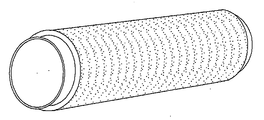
본 발명은 캐리어 튜브와, 캐리어 튜브 상에 배치된 인듐계 스퍼터링 재료를 갖는 튜브형 스퍼터링 타겟에 관한 것이다. The present invention relates to a tubular sputtering target having a carrier tube and an indium-based sputtering material disposed on the carrier tube.
예컨대, 인듐 튜브 타겟은 CuInGaS2 또는 CuInGaSe2에 기초하는 박층 광전지를 위해 CuInGa 흡수재 층을 코팅하는데 사용된다. 인듐 스퍼터링은, 다른 스퍼터링 비율을 유발함으로써 입자 배향의 함수로서 층의 불균등한 두께를 유발하는 스퍼터링 타겟의 표면 상의 니들형 구조의 형성과 종종 관련된다(엠. 베이게르트(M. Weigert), CIGS 스퍼터링의 문제점, 헤레우스 박막 재료 No.11, 2008년 4월). 지금까지, 대응하는 튜브 타겟은 예컨대, 유럽 특허 제1186682 B1호에 개시된 바와 같은 단순한 주조법을 통해 제조되어 왔다. CIGS 적용을 위해서는 금속이 고순도(99.99% 내지 99.999%)일 필요가 있는데, 상술된 스퍼터링 타겟은 매우 조악한 구조를 가져, 상술된 문제를 야기할 수도 있다. For example, an indium tube target is used to coat a CuInGa absorber layer for thin photovoltaic cells based on CuInGaS 2 or CuInGaSe 2 . Indium sputtering is often associated with the formation of a needle-like structure on the surface of the sputtering target that causes different sputtering ratios, resulting in uneven thickness of the layer as a function of particle orientation (M. Weigert, CIGS sputtering Problem, Heraeus thin film material No.11, April 2008). To date, corresponding tube targets have been produced via a simple casting process as disclosed, for example, in European Patent No. 1 186682 B1. For CIGS applications, the metal needs to be of high purity (99.99% to 99.999%), which the sputtering targets described above have very coarse structures, which may cause the problems described above.
본 발명의 목적은 균등한 스퍼터링 비율 및 균등한 두께의 층을 달성하기 위해 공지된 스퍼터링 타겟을 개선하는 것이다. It is an object of the present invention to improve known sputtering targets in order to achieve even sputtering ratios and equally thick layers.
이런 목적은 독립항들의 구성요소를 통해 달성된다. 유리한 실시예들이 종속항에 특정되어 있다. 특히, 본 발명은, 캐리어 튜브와, 캐리어 튜브 상에 배치된 인듐계 스퍼터링 재료를 갖고, 스퍼터링 재료는 스퍼터링 재료의 스퍼터링되어 거칠어진(sputtering-roughened) 표면 상의 입자의 평균 직경으로서 측정된 1mm 미만의 평균 입자 크기를 갖는 마이크로구조체를 갖는 것을 특징으로 하는 튜브형 스퍼터링 타겟으로 특징지어진다.. This object is achieved through the components of the independent claims. Advantageous embodiments are specified in the dependent claims. In particular, the present invention has a carrier tube and an indium-based sputtering material disposed on the carrier tube, the sputtering material being less than 1 mm measured as the average diameter of particles on the sputtered-roughened surface of the sputtering material. And a tubular sputtering target characterized by having a microstructure with an average particle size.
선택적으로, 스퍼터링 재료는 주석, 아연의 그룹으로부터의 적어도 하나의 금속을 포함할 수 있다. 특히, 스퍼터링 재료는 최대 중량1%의 분율의 구리 및/또는 갈륨을 포함한다. 또한, 마이크로구조체의 평균 입자 크기는 500㎛ 미만, 바람직하게는 200㎛ 미만인 것이 바람직하다. 또한, 스퍼터링 재료의 액상선 온도는 350℃ 이하인 것이 유리하다. Optionally, the sputtering material may comprise at least one metal from the group of tin, zinc. In particular, the sputtering material comprises a fraction of copper and / or gallium up to 1% by weight. In addition, the average particle size of the microstructures is preferably less than 500 μm, preferably less than 200 μm. In addition, the liquidus temperature of the sputtering material is advantageously 350 ° C. or less.
또한, 스퍼터링 재료의 평균 입자 크기는 타겟 표면으로부터 캐리어 튜브 위 적어도 1mm까지 반경 방향으로 측정된 바와 같이 스퍼터링 재료의 두께를 가로질러 달성되는 것이 유리하다. 본 명세서에서 이후에 기술될 대응하는 특정 치수와 관련하여, 적어도 1mm의 거리란 캐리어 튜브의 외부면으로부터 측정된 거리, 또는 바람직하게는 캐리어 튜브와 스퍼터링 재료 사이에 배치되는 층(예컨대, 접착 증진제, 땜납 층)의 외부면으로부터 측정된 거리를 지칭하며, 이런 거리는 반경 방향 외향으로 측정되어야 한다. In addition, the average particle size of the sputtering material is advantageously achieved across the thickness of the sputtering material as measured radially from the target surface to at least 1 mm above the carrier tube. With respect to the corresponding specific dimensions to be described later herein, the distance of at least 1 mm means the distance measured from the outer surface of the carrier tube, or preferably a layer (eg, adhesion promoter, disposed between the carrier tube and the sputtering material, Refers to the distance measured from the outer surface of the solder layer), which distance should be measured radially outward.
바람직하게는, 스퍼터링 재료의 금속의 순도는 적어도 99.99%, 보다 바람직하게는 99.999%이다. 다른 유리한 실시예에서, 스퍼터링 재료는 스퍼터링 재료에 대면하는 캐리어 튜브의 표면으로부터 적어도 1mm보다 큰 거리에 균질 마이크로구조체를 포함한다. Preferably, the purity of the metal of the sputtering material is at least 99.99%, more preferably 99.999%. In another advantageous embodiment, the sputtering material comprises a homogeneous microstructure at a distance greater than at least 1 mm from the surface of the carrier tube facing the sputtering material.
입자의 적어도 90%는 평균 입자 크기의 +/- 70%, 바람직하게는 +/- 50%의 범위의 크기인 것이 바람직하다. 특히, 스퍼터링 재료의 마이크로구조체의 입자는 각각 최소 직경 및 최대 직경을 가지며, 복수의 입자의 최대 직경 대 최소 직경의 비율은 1.5보다 큰, 바람직하게는 2보다 큰, 특히 3보다 큰 것이 유리하다. 본 명세서에서, 적어도 복수의 입자는 구형을 벗어난 형상을 갖는 것이 바람직하다. 본 명세서에서, 형상은 하나 이상의 방향에서 편평화되거나 클린치된 또는 임의의 다른 방향에서 변형된 구체의 형상일 수 있다. At least 90% of the particles are preferably in the range of +/- 70%, preferably +/- 50% of the average particle size. In particular, the particles of the microstructure of the sputtering material each have a minimum diameter and a maximum diameter, and the ratio of the maximum diameter to the minimum diameter of the plurality of particles is advantageously greater than 1.5, preferably greater than 2, in particular greater than 3. In the present specification, it is preferable that at least a plurality of particles have a shape out of a sphere. In the present specification, the shape may be the shape of a sphere that is flattened or clinched in one or more directions or modified in any other direction.
유리하게는, 스퍼터링 재료의 밀도는 이론 밀도의 적어도 90%, 특히 적어도 95%이다. 또한, 스퍼터링 재료의 각각의 입자는 산화물 층을 통해 표면 상에 부통태화되는 것이 바람직하다. 바람직하게는, 스퍼터링 재료의 산소 함유량은 전체 스퍼터링 재료에 대해 50ppm 내지 500ppm의 범위, 보다 바람직하게는 70ppm 내지 300ppm의 범위일 수 있다. Advantageously, the density of the sputtering material is at least 90%, in particular at least 95% of the theoretical density. In addition, each particle of the sputtering material is preferably passivated on the surface through the oxide layer. Preferably, the oxygen content of the sputtering material may be in the range of 50 ppm to 500 ppm, more preferably in the range of 70 ppm to 300 ppm relative to the total sputtering material.
캐리어 튜브는 비자성 재료로, 보다 바람직하게는 비자성 강합금으로 제조될 수 있으며, 캐리어 튜브의 재료는 바람직하게는 비자성 강합금이고, 스퍼터링 재료의 철 함유량은, 캐리어 튜브로부터 또는 스퍼터링 재료와 캐리어 튜브 사이에 배치될 수도 있는 접착 증진제의 층으로부터 최소 1mm의 거리에서 측정된, 스퍼터링 재료의 개시 재료의 철 함유량보다 높은, 5ppm 이하, 바람직하게는 1ppm 이하이다. 스퍼터링 타겟의 길이는 바람직하게는 적어도 500mm일 수 있다. The carrier tube may be made of a nonmagnetic material, more preferably of a nonmagnetic steel alloy, the material of the carrier tube is preferably a nonmagnetic steel alloy, and the iron content of the sputtering material is from the carrier tube or with the sputtering material. 5 ppm or less, preferably 1 ppm or less, higher than the iron content of the starting material of the sputtering material, measured at a distance of at least 1 mm from the layer of adhesion promoter that may be disposed between the carrier tubes. The length of the sputtering target may preferably be at least 500 mm.
본 발명에 따르면, 스퍼터링 타겟은 광기전 흡수재(photovoltaic absorber)의 층을 직접 또는 다단계 프로세스로 증착시키기 위해 또는 반응성 스퍼터링을 통해 산화물 층을 증착시키기 위해 사용될 수 있다. In accordance with the present invention, sputtering targets can be used to deposit a layer of photovoltaic absorbers directly or in a multi-step process, or to deposit an oxide layer through reactive sputtering.
전반적으로, 본 발명은 미립자 크기와 고밀도를 갖는 인듐(In) 또는 In 합금으로 제조된 고순도(99.99% 내지 99.999%의 순도) 튜브 타겟을 제공할 수 있다. 또한, 산소 함유량은, 한편으론 음극에서의 스파크 오버(spark-over)(아킹(arcing)) 또는 스퍼터링 동안의 니들 형성이나 픽업이 없고, 다른 한편으론 아킹이 어쨌든 유발되는 경우에 타겟 재료가 타겟 재료의 많은 영역에 걸쳐 즉시 용융되지 않도록 선택될 수 있다. 따라서, 개시 재료 대 유용 타겟 재료의 양호한 비율이 달성될 수 있다. Overall, the present invention can provide a high purity (99.99% to 99.999% purity) tube target made of indium (In) or In alloy having particulate size and high density. In addition, the oxygen content of the target material on the one hand does not have spark-over (arking) or needle formation or pick-up during sputtering on the cathode, and on the other hand the target material is the target material when arcing is caused anyway. It may be chosen such that it does not melt immediately over many areas of the. Thus, a good ratio of starting material to useful target material can be achieved.
따라서, 본 발명에 따른 스퍼터링 타겟은 바람직하게는 다음과 같은 특징들 중 하나 이상의 특징을 포함한다: Thus, the sputtering target according to the invention preferably comprises one or more of the following features:
- 적어도 99.99%, 바람직하게는 적어도 99.999%의 순도,A purity of at least 99.99%, preferably at least 99.999%,
- 스퍼터링 에칭된 튜브 표면 상의 인듐 입자의 평균 직경으로부터 측정된 바와 같이, 1mm 미만, 바람직하게는 500㎛ 미만, 보다 바람직하게는 200㎛ 미만의 평균 입자 크기를 갖고, 평균 입자 크기는 타겟 표면으로부터 캐리어 튜브 위 1mm까지 달성되는 미립 마이크로구조체,Having an average particle size of less than 1 mm, preferably less than 500 μm, more preferably less than 200 μm, as measured from the average diameter of the indium particles on the sputter etched tube surface, the average particle size being a carrier from the target surface Particulate microstructures up to 1 mm above the tube,
- 입자의 90%의 입자 크기가 평균 입자 크기의 +/- 70%, 바람직하게는 +/- 50%의 범위이고, (캐리어 튜브에 가장 가까운 마지막 1mm를 제외하곤) 타겟의 길이 및 두께를 따라 균질인 마이크로구조체,90% of the particle size is in the range of +/- 70%, preferably +/- 50% of the average particle size, and along the length and thickness of the target (except for the last 1 mm closest to the carrier tube) Homogeneous microstructure,
- 직경/두께 비율이 2보다 크고 렌즈형 단면을 갖는 입자 형상,A particle shape having a diameter / thickness ratio greater than 2 and having a lenticular cross section,
- 이론 밀도의 90%, 바람직하게는 95%보다 큰 밀도,A density greater than 90% of the theoretical density, preferably greater than 95%,
- 아킹이 유발되는 경우 용융 성향을 감소시키기 위해 얇은 산화물 층을 통한 각각의 입자의 표면 부동태화,Surface passivation of each particle through a thin layer of oxide to reduce melting tendency when arcing is induced,
- 50ppm 내지 500ppm의 범위, 바람직하게는 70ppm 내지 300ppm의 범위인 산소 함유량,An oxygen content in the range from 50 ppm to 500 ppm, preferably in the range from 70 ppm to 300 ppm,
- 조성: (불순물을 포함하는)인듐, 300℃ 미만의 용융 온도를 갖는 인듐 합금, 특히 In-Sn,Composition: indium (including impurities), indium alloys having a melting temperature below 300 ° C., in particular In—Sn,
- 스퍼터링 타겟 재료의 철 함유량은 제조시 사용된 개시 재료의 철 함유량에 비해 5ppm / 1ppm 이상 증가되지 않는, 인듐 재료와 스테인레스강 캐리어 튜브의 합성물. Composite of indium material and stainless steel carrier tube, wherein the iron content of the sputtering target material does not increase by more than 5 ppm / 1 ppm relative to the iron content of the starting material used in the manufacture.
본 발명에 따르면, 균등한 스퍼터링 비율 및 균등한 두께의 층을 달성할 수 있는 스퍼터링 타겟과, 미립자 크기와 고밀도를 갖는 인듐(In) 또는 In 합금으로 제조된 고순도(99.99% 내지 99.999%의 순도) 튜브 타겟을 제공할 수 있다. According to the present invention, a sputtering target capable of achieving an even sputtering ratio and an equal thickness of layers, and high purity (purity of 99.99% to 99.999%) made of indium (In) or In alloy having fine particle size and high density Tube targets may be provided.
도 1a는 본 발명에 따른 마이크로구조체를 갖는 방법 1에 따른 미립 타겟을 도시하는 도면.
도 1b는 방법 1에 따른 인듐 튜브 타겟의 스퍼터링 에칭된 표면을 도시하는 도면.
도 2는 4㎾/m의 비출력에서 본 발명에 따른 타겟에 대한 시간의 함수로서의 스퍼터링 비율을 도시하는 도면.
도 3은 조립(coarse-grained) 마이크로구조체를 갖는 방법 2에 따른 스퍼터링 타겟(참조 타겟)을 도시하는 도면.
도 4는 4㎾/m의 비출력에서 방법 2에 따른 타겟(참조 타겟)에 대한 시간의 함수로서의 스퍼터링 비율을 도시하는 도면. 1a shows a particulate target according to
FIG. 1B shows a sputter etched surface of an indium tube target according to
2 shows the sputtering ratio as a function of time for a target according to the invention at a specific power of 4 dB / m.
3 shows a sputtering target (reference target) according to
4 shows the sputtering ratio as a function of time for a target (reference target) according to
1. 본 발명에 따른 튜브 타겟을 위한 방법1. Method for the tube target according to the invention
고순도 인듐(99.999%)이 도가니에서 용융되었다. 거친 접착 증진제 층을 구비한 캐리어 튜브가 회전 장치 상에 장착되었다. 액체 용융 인듐 금속이 공급 라인을 통해 분무기 노즐로 공급되어, 가스의 작용을 통해 분무되었다. 액체 용융 액적이 회전하는 캐리어 튜브에 충돌함으로써, 캐리어 튜브 대 분무 노즐의 상대 운동이 시간이 지남에 따라 두꺼운 금속 인듐 층을 캐리어 튜브 상에 복수의 층의 형태로 증착시킨다. 용융물의 최적의 온도는 노즐 기하학적 구조, 분무 거리 및 캐리어 튜브의 원주 속도의 함수로서 임의의 예비 실험으로 결정되어야 한다. 170℃ 내지 230℃의 범위의 온도가 유리한 것으로 입증되었다. 아르곤 및 질소와 같은 보호 가스 및 공기가 분무기 가스로서 사용될 수 있다. 용융 온도 및 분무 거리와 함께 가스의 적절한 선택은 유효 산소 함유량이 스퍼터링 타겟 재료 내에서 조절될 수 있게 한다. 또한 이를 위해서는, 선택되는 용액에 따라 임의의 예비 실험이 필요하다. 따라서, 제조된 튜브 블랭크는 오버 트위스팅(over-twisting)에 의해 제거된 분무에 의한 거친 표면을 여전히 갖는다. High purity indium (99.999%) was melted in the crucible. A carrier tube with a rough adhesion promoter layer was mounted on the rotating device. Liquid molten indium metal was supplied to the nebulizer nozzle through the supply line and sprayed through the action of gas. By impinging the molten liquid droplets on the rotating carrier tube, the relative movement of the carrier tube to the spray nozzle over time deposits a thick layer of metal indium in the form of a plurality of layers on the carrier tube. The optimum temperature of the melt should be determined by any preliminary experiment as a function of nozzle geometry, spray distance and circumferential velocity of the carrier tube. Temperatures in the range of 170 ° C. to 230 ° C. have proven advantageous. Protective gases such as argon and nitrogen and air can be used as the nebulizer gas. Proper selection of the gas along with the melting temperature and spraying distance allows the effective oxygen content to be controlled in the sputtering target material. This also requires some preliminary experimentation depending on the solution chosen. Thus, the tube blanks produced still have a rough surface by spraying removed by over-twisting.
제조 파라미터가 적절히 선택되면, 본 발명에 따른 마이크로구조체가 달성된다. 당업자는 일련의 실험을 통해 본 발명에 따른 마이크로구조체를 용이하게 달성할 수 있지만, 본 발명에 따른 입자 크기 및 산소 함유량 성질을 달성하기 위해서는 온도 및 대기에 특별한 주의를 기울여야 한다. 코팅 파라미터가 부적절하게 선택된 경우, 최종 밀도가 너무 낮았거나(90% 미만) 산소 함유량이 너무 높았다(500ppm 초과). If the production parameters are properly selected, the microstructures according to the invention are achieved. A person skilled in the art can easily achieve the microstructures according to the invention through a series of experiments, but special attention must be paid to temperature and atmosphere to achieve the particle size and oxygen content properties according to the invention. If the coating parameters were improperly selected, the final density was too low (less than 90%) or the oxygen content was too high (greater than 500 ppm).
따라서, 제조된 튜브는 프로세스 파라미터에 따라 평균 입자 크기가 50㎛ 내지 500㎛인 미립자 마이크로구조체를 가졌다. 대부분의 경우, 최종 평균 입자 크기는 200㎛ 미만이었다. 입자 크기는 각각의 경우(도 1a, 도 1b) 1mm 미만이었다. 본 발명에 따라 스퍼터링 타겟을 층의 형태로 제조하기 때문에, 마이크로구조체는 스퍼터링 타겟의 두께 및 재킷 표면을 가로질러 균질이다. 평균 입자 크기는 스퍼터링 타겟을 가로질러 길이 및 두께에 있어서 +/- 70% 이하로 변화되었지만, 대부분의 경우 단지 +/- 50% 미만으로 변화되었다. 또한, 입자는 통상 2를 초과하는 범위의, 종종 3을 초과하는 범위의 직경 대 두께의 비율을 갖는 편평한 형상을 가졌다. 미세하고 균질인 입자 크기 및 편평한 입자 형상으로 인해, 스퍼터링 동안 각각의 입자의 노출 시간은 입자가 제거될 때까지였지만, 단시간이었다. 그 결과, 상술된 니들 구조는 넓은 영역에 걸쳐 달성될 수가 없다. 따라서, 최종 스퍼터링 비율(증착률)은 매우 안정적이었다(도 2 참조). 양호한 실시예에서, 15mm 두께의 인듐 코팅을 갖는 튜브 타겟에 대해서도 대략 20㎾/m까지 특유한 스퍼터링 로드(sputtering load)를 실시할 수 있었다. 따라서, 스퍼터링 타겟은 적어도 15㎾/m, 가능하게는 20㎾/m 이상의 비출력으로 작동될 수 있다. Thus, the tubes produced had particulate microstructures with an average particle size of 50 μm to 500 μm, depending on the process parameters. In most cases, the final average particle size was less than 200 μm. The particle size was less than 1 mm in each case (FIGS. 1A, 1B). Since the sputtering target is produced in the form of a layer according to the invention, the microstructures are homogeneous across the thickness and the jacket surface of the sputtering target. Average particle size varied below +/- 70% in length and thickness across the sputtering target, but in most cases only changed below +/- 50%. In addition, the particles usually had a flat shape with a ratio of diameter to thickness in the range of more than two, often in the range of more than three. Due to the fine and homogeneous particle size and flat particle shape, the exposure time of each particle during sputtering was until the particles were removed, but for a short time. As a result, the needle structure described above cannot be achieved over a wide area. Therefore, the final sputtering ratio (deposition rate) was very stable (see FIG. 2). In a preferred embodiment, specific sputtering loads could be applied up to approximately 20 kW / m even for tube targets with 15 mm thick indium coating. Thus, the sputtering target can be operated with a specific power of at least 15 kW / m, possibly 20 kW / m or more.
프로세스 조건을 적절히 선택함으로써, 50ppm 내지 500ppm의 범위의 산소 값이 달성될 수 있었다. 스퍼터링 동안 특히 실행된 아킹은, 더 깊어질수록 산소 함유량이 더 낮아지는 낮은 용융 인듐의 트레이스를 생성한다는 것을 놀랍게도 발견하였다. 따라서, 입자 주위의 산화물 쉘은 단시간의 용융 동안 스퍼터링 타겟 표면을 안정화시킨다. 유리한 산소 함유량은 70ppm 내지 300ppm의 범위라는 것을 발견하였다. 어느 정도의 제한은 있지만, 50ppm 내지 500ppm의 범위도 또한 사용될 수 있다. 본 명세서에서 산소는 파티클 및/또는 입자 주의에 산화물 쉘의 형태로 존재한다는 것이 중요하다. 용융 안정화의 유리한 효과는 O2 값이 너무 낮은 경우에는 더 이상 나타나지 않는다. O2 값이 너무 높은 경우에는, 산화물에 의한 불안정이 분명히 유발되기 때문에, 바람직하지 않은 아킹을 야기한다. 기술된 바와 같이 제조된 타겟의 철 함유량은 캐리어 튜브 및/또는 캐리어 튜브와 스퍼터링 재료 사이에 배치된 접착층 위 적어도 1mm에서 취한 샘플인 경우 1ppm 미만이었다. 산 용해된 스퍼터링 타겟 재료 상의 불순물은 광학적 방출 분광법(OES) 및 유도 결합 플라즈마(ICP)를 통한 여기를 이용하여 시금되었다. By appropriate selection of process conditions, oxygen values in the range of 50 ppm to 500 ppm could be achieved. It has surprisingly been found that arcing, especially carried out during sputtering, produces traces of low molten indium with deeper lower oxygen content. Thus, the oxide shell around the particles stabilizes the sputtering target surface for a short time of melting. The advantageous oxygen content was found to be in the range of 70 ppm to 300 ppm. With some limitations, a range of 50 ppm to 500 ppm may also be used. It is important here that oxygen is present in the form of oxide shells in particle and / or particle attention. The beneficial effect of melt stabilization no longer appears when the O 2 value is too low. If the O 2 value is too high, unstable by oxides are clearly caused, which leads to undesirable arcing. The iron content of the target prepared as described was less than 1 ppm for a sample taken at least 1 mm above the carrier tube and / or the adhesive layer disposed between the carrier tube and the sputtering material. Impurities on the acid dissolved sputtering target material were assayed using excitation through optical emission spectroscopy (OES) and inductively coupled plasma (ICP).
대안적으로, 순수 인듐 대신 예컨대, In:Cu, In:Ga, In:Sn 또는 In:Zn, 또는 이들의 혼합물과 같은 인듐 합금을 사용할 수 있다. 본 발명에 따른 방법은 합금의 액상선 온도가 350℃를 초과하지 않는다면 성공적으로 달성된다. 공융 혼합물이 상당히 적기 때문에, 최대 중량5% 내지 중량10%까지 In:Ga만을 첨가제로서 사용할 수 있다. In:Cu의 사용은 액상선 온도가 급격히 상승하기 때문에 최대로 대략 중량5%로 제한된다. Alternatively, indium alloys such as In: Cu, In: Ga, In: Sn or In: Zn, or mixtures thereof may be used instead of pure indium. The process according to the invention is successfully achieved if the liquidus temperature of the alloy does not exceed 350 ° C. Since the eutectic mixture is quite small, only In: Ga up to 5% to 10% by weight can be used as additive. The use of In: Cu is limited to a maximum of approximately 5% by weight because the liquidus temperature rises sharply.
2. 대안적인 튜브 타겟(참조예)을 위한 방법2. Method for an alternative tube target (reference example)
참조예의 주조 제조법은 99.999% 순도 인듐이 사용되었다는 것을 제외하곤 유럽 특허 제1186682 B1호에 개시된 주석(Sn) 튜브에 대해 기재된 방법에 대응한다. 인듐은 용융되어 캐리어 튜브를 둘러싸는 예열된 강철 주형 내의 도가니로부터 190℃에서 주조되었으며, 강철 주형의 최하부는 밀봉부를 통해 캐리어 튜브에 연결되었다. 또한, 주조 주형은 산화를 방지하기 위해 보호 가스로 세척되었다. 캐리어 튜브에 대한 인듐의 접합을 향상시키기 위해, 캐리어 튜브에는 인듐 땜납이 사전 구비된 니켈계 접착층이 구비되어 있었다. 주조 후, 캐리어 튜브는 최종 응고가 바닥부로부터 상부까지 진행되도록 유입 공기를 사용하여 최하부를 기점으로 내부로부터 냉각되었다. 이런 방법에 따라 조립 인듐 튜브 타겟(도 3 참조)이 달성되었는데, 용융물이 장기간 캐리어 튜브 및 주조 주형에 접촉되었기 때문에 최종 철 함유량은 역시 50ppm으로 너무 높았다. 상술된 니들 구조가 표면 상에 형성되었기 때문에, 조악한 마이크로구조체는 도 4에 도시된 바와 같이 시간이 지남에 따라 스퍼터링 비율이 크게 감소되었다. 스퍼터링 타겟은 무시할 수 있을 정도의 아킹으로만 스퍼터링되었다. 그러나, 50ppm 미만의 낮은 산소 함유량은 타겟 표면에 인공적으로 생성된 아킹에 의해 형성된 심공을 유발하였다. 넓은 기술적 범위에 걸친 스퍼터링 프로세스는 아킹에 대한 외부 요인과 주기적으로 관련되기 때문에, 인듐만큼 낮은 재료 용융의 경우에 특히 위험이 증가된다. The casting preparation of the reference example corresponds to the method described for tin (Sn) tubes disclosed in EP 1668668 B1, except that 99.999% purity indium was used. Indium was melted and cast at 190 ° C. from a crucible in a preheated steel mold surrounding the carrier tube, and the bottom of the steel mold was connected to the carrier tube via a seal. In addition, the casting molds were washed with a protective gas to prevent oxidation. In order to improve the bonding of indium to the carrier tube, the carrier tube was provided with a nickel-based adhesive layer pre-equipped with indium solder. After casting, the carrier tube was cooled from the inside starting at the lowest point using inlet air so that final solidification proceeded from the bottom to the top. In this way, an assembled indium tube target (see FIG. 3) was achieved, the final iron content being too high at 50 ppm as the melt was in contact with the carrier tube and casting mold for a long time. Since the needle structure described above was formed on the surface, the coarse microstructures had a greatly reduced sputtering rate over time as shown in FIG. 4. Sputtering targets were only sputtered with negligible arcing. However, a low oxygen content of less than 50 ppm caused deep holes formed by artificially generated arcing on the target surface. Since the sputtering process over a wide technical range is periodically related to external factors for arcing, the risk is particularly increased in the case of material melting as low as indium.
Claims (18)
스퍼터링 재료는 최대 중량1%의 분율의 구리 및/또는 갈륨을 포함하는 것을 특징으로 하는, 튜브형 스퍼터링 타겟. A tubular sputtering target having a carrier structure and a microstructure having an indium-based sputtering material disposed on the carrier tube, the sputtering material having an average particle size of less than 1 mm measured as the average diameter of particles on the sputtered roughened surface of the sputtering material. To
A sputtering target, characterized in that the sputtering material comprises a fraction of copper and / or gallium up to 1% by weight.
스퍼터링 재료의 철 함유량은, 캐리어 튜브로부터 또는 스퍼터링 재료와 캐리어 튜브 사이에 배치될 수도 있는 접착 증진제의 층으로부터 최소 1mm의 거리에서 측정된, 스퍼터링 재료의 개시 재료의 철 함유량보다 높은, 5ppm 이하, 바람직하게는 1ppm 이하인 것을 특징으로 하는, 튜브형 스퍼터링 타겟. The material of claim 14, wherein the material of the carrier tube is a nonmagnetic steel alloy,
The iron content of the sputtering material is 5 ppm or less, preferably higher than the iron content of the starting material of the sputtering material, measured at a distance of at least 1 mm from the carrier tube or from a layer of adhesion promoter that may be disposed between the sputtering material and the carrier tube. Tubular sputtering target, characterized in that less than 1ppm.
Applications Claiming Priority (2)
| Application Number | Priority Date | Filing Date | Title |
|---|---|---|---|
| DE102011012034A DE102011012034A1 (en) | 2011-02-22 | 2011-02-22 | Tubular sputtering target |
| DE102011012034.3 | 2011-02-22 |
Publications (1)
| Publication Number | Publication Date |
|---|---|
| KR20120096426A true KR20120096426A (en) | 2012-08-30 |
Family
ID=45507397
Family Applications (1)
| Application Number | Title | Priority Date | Filing Date |
|---|---|---|---|
| KR1020120016571A KR20120096426A (en) | 2011-02-22 | 2012-02-17 | Tube-shaped sputtering target |
Country Status (8)
| Country | Link |
|---|---|
| US (1) | US9334564B2 (en) |
| EP (1) | EP2492368B1 (en) |
| JP (1) | JP5777539B2 (en) |
| KR (1) | KR20120096426A (en) |
| CN (1) | CN102644053B (en) |
| DE (1) | DE102011012034A1 (en) |
| PL (1) | PL2492368T3 (en) |
| TW (1) | TWI527923B (en) |
Families Citing this family (18)
| Publication number | Priority date | Publication date | Assignee | Title |
|---|---|---|---|---|
| JP4948634B2 (en) | 2010-09-01 | 2012-06-06 | Jx日鉱日石金属株式会社 | Indium target and manufacturing method thereof |
| JP5140169B2 (en) | 2011-03-01 | 2013-02-06 | Jx日鉱日石金属株式会社 | Indium target and manufacturing method thereof |
| JP5026611B1 (en) | 2011-09-21 | 2012-09-12 | Jx日鉱日石金属株式会社 | Laminated structure and manufacturing method thereof |
| JP5074628B1 (en) * | 2012-01-05 | 2012-11-14 | Jx日鉱日石金属株式会社 | Indium sputtering target and method for manufacturing the same |
| KR20160085907A (en) * | 2012-08-22 | 2016-07-18 | 제이엑스금속주식회사 | Cylindrical indium sputtering target and process for producing same |
| US20140110245A1 (en) * | 2012-10-18 | 2014-04-24 | Primestar Solar, Inc. | Non-bonded rotatable targets and their methods of sputtering |
| TWI461556B (en) * | 2012-10-24 | 2014-11-21 | Solar Applied Mat Tech Corp | Indium target with tetragonal structure |
| CN103789729A (en) * | 2012-10-31 | 2014-05-14 | 光洋应用材料科技股份有限公司 | Indium target material with tetragonal crystal structure |
| JP5968808B2 (en) * | 2013-03-07 | 2016-08-10 | Jx金属株式会社 | Indium cylindrical target member and method of manufacturing cylindrical target member |
| US9922807B2 (en) * | 2013-07-08 | 2018-03-20 | Jx Nippon Mining & Metals Corporation | Sputtering target and method for production thereof |
| JP6217295B2 (en) * | 2013-10-07 | 2017-10-25 | 三菱マテリアル株式会社 | In sputtering target |
| JP6305083B2 (en) * | 2014-02-04 | 2018-04-04 | Jx金属株式会社 | Sputtering target and manufacturing method thereof |
| EP2947175A1 (en) * | 2014-05-21 | 2015-11-25 | Heraeus Deutschland GmbH & Co. KG | CuSn, CuZn and Cu2ZnSn sputter targets |
| EP3085809B1 (en) | 2015-04-20 | 2018-07-18 | Materion Advanced Materials Germany GmbH | Process for preparing a tubular sputtering target |
| JP6456810B2 (en) * | 2015-12-11 | 2019-01-23 | Jx金属株式会社 | In-Cu alloy sputtering target and method for producing the same |
| JP2017141515A (en) * | 2017-03-17 | 2017-08-17 | Jx金属株式会社 | Sputtering target, and its production |
| US11450516B2 (en) | 2019-08-14 | 2022-09-20 | Honeywell International Inc. | Large-grain tin sputtering target |
| CN112030119A (en) * | 2020-08-27 | 2020-12-04 | 苏州思菲科新材料科技有限公司 | Indium tube target and preparation method thereof |
Family Cites Families (35)
| Publication number | Priority date | Publication date | Assignee | Title |
|---|---|---|---|---|
| JPS60234968A (en) | 1984-05-07 | 1985-11-21 | Nippon Mining Co Ltd | Bonded target and its manufacture |
| DE4115663A1 (en) * | 1991-05-14 | 1992-11-19 | Leybold Ag | Target mfr. for a sputtering device - by plasma-spraying a metal, alloy or cpd. on to a target substrate |
| JPH05171428A (en) | 1991-12-12 | 1993-07-09 | Mitsubishi Materials Corp | Columnar target for sputtering |
| JPH06264233A (en) | 1993-03-12 | 1994-09-20 | Nikko Kinzoku Kk | Sputtering target for producing tft |
| JPH0726373A (en) * | 1993-07-09 | 1995-01-27 | Asahi Glass Co Ltd | Rotating cathode target, its production and film formed by using this target |
| JPH08218164A (en) | 1995-02-13 | 1996-08-27 | Toshiba Corp | Sputtering target for forming soft magnetic thin film |
| JP3462927B2 (en) | 1995-03-16 | 2003-11-05 | 株式会社日立製作所 | Film forming apparatus, jig for film forming apparatus, and film forming method |
| JP3840735B2 (en) | 1996-04-12 | 2006-11-01 | 旭硝子株式会社 | Manufacturing method of oxide film |
| US5942090A (en) | 1996-04-12 | 1999-08-24 | Asahi Glass Company Ltd. | Methods of producing a laminate |
| JPH1068072A (en) | 1996-08-26 | 1998-03-10 | Japan Energy Corp | Ito cylindrical target and its production |
| JPH10130827A (en) | 1996-10-28 | 1998-05-19 | Mitsubishi Materials Corp | Mgo target and its production |
| JPH10195609A (en) | 1996-12-27 | 1998-07-28 | Dowa Mining Co Ltd | Fcc metal in which crystal orientation is regulated and its production |
| JPH11269637A (en) | 1998-03-24 | 1999-10-05 | Sumitomo Metal Mining Co Ltd | Production of large-sized sputtering target |
| DE10043748B4 (en) | 2000-09-05 | 2004-01-15 | W. C. Heraeus Gmbh & Co. Kg | Cylindrical sputtering target, process for its production and use |
| DE10063383C1 (en) | 2000-12-19 | 2002-03-14 | Heraeus Gmbh W C | Production of a tubular target used for cathode sputtering devices comprises forming an outer tube by casting a molten material in a mold, in which the mold has a heated core rod formed from an inner tube |
| JP4836359B2 (en) | 2001-06-28 | 2011-12-14 | 株式会社東芝 | Sputter target, gate insulating film and electronic parts |
| CN1289709C (en) | 2001-08-13 | 2006-12-13 | 贝卡尔特股份有限公司 | Method for mfg. sputter target |
| AU2003275239A1 (en) * | 2002-09-30 | 2004-04-23 | Miasole | Manufacturing apparatus and method for large-scale production of thin-film solar cells |
| JP4263900B2 (en) | 2002-11-13 | 2009-05-13 | 日鉱金属株式会社 | Ta sputtering target and manufacturing method thereof |
| US20050279630A1 (en) * | 2004-06-16 | 2005-12-22 | Dynamic Machine Works, Inc. | Tubular sputtering targets and methods of flowforming the same |
| JP4650315B2 (en) | 2005-03-25 | 2011-03-16 | 株式会社ブリヂストン | Method for forming In-Ga-Zn-O film |
| DE102006055662B3 (en) | 2006-11-23 | 2008-06-26 | Gfe Metalle Und Materialien Gmbh | Coating material based on a copper-indium-gallium alloy, in particular for the production of sputtering targets, tube cathodes and the like |
| JP5215192B2 (en) | 2007-01-05 | 2013-06-19 | 株式会社東芝 | Sputtering target |
| US8197894B2 (en) | 2007-05-04 | 2012-06-12 | H.C. Starck Gmbh | Methods of forming sputtering targets |
| CN103030381B (en) * | 2007-07-06 | 2015-05-27 | 住友金属矿山株式会社 | Oxide sintered body and production method therefor, target, and transparent conductive film and transparent conductive substrate obtained by using the same |
| JP4957968B2 (en) | 2007-11-12 | 2012-06-20 | 三菱マテリアル株式会社 | Cu-In-Ga ternary sintered alloy sputtering target and method for producing the same |
| JP4957969B2 (en) | 2007-11-12 | 2012-06-20 | 三菱マテリアル株式会社 | Method for producing Cu-In-Ga ternary sintered alloy sputtering target |
| US20100108503A1 (en) * | 2008-10-31 | 2010-05-06 | Applied Quantum Technology, Llc | Chalcogenide alloy sputter targets for photovoltaic applications and methods of manufacturing the same |
| US20100200395A1 (en) * | 2009-02-06 | 2010-08-12 | Anton Dietrich | Techniques for depositing transparent conductive oxide coatings using dual C-MAG sputter apparatuses |
| DE102009015638A1 (en) * | 2009-03-24 | 2010-09-30 | Wieland Dental + Technik Gmbh & Co. Kg | Tubular sputtering target and method for its production |
| US7785921B1 (en) | 2009-04-13 | 2010-08-31 | Miasole | Barrier for doped molybdenum targets |
| EP2287356A1 (en) * | 2009-07-31 | 2011-02-23 | Bekaert Advanced Coatings NV. | Sputter target, method and apparatus for manufacturing sputter targets |
| JP5149262B2 (en) | 2009-11-05 | 2013-02-20 | 出光興産株式会社 | Indium oxide-zinc oxide sintered target and method for producing the same |
| JP5254290B2 (en) | 2010-09-01 | 2013-08-07 | Jx日鉱日石金属株式会社 | Indium target and manufacturing method thereof |
| JP4948634B2 (en) | 2010-09-01 | 2012-06-06 | Jx日鉱日石金属株式会社 | Indium target and manufacturing method thereof |
-
2011
- 2011-02-22 DE DE102011012034A patent/DE102011012034A1/en not_active Withdrawn
-
2012
- 2012-01-12 EP EP12000166.4A patent/EP2492368B1/en active Active
- 2012-01-12 PL PL12000166T patent/PL2492368T3/en unknown
- 2012-02-03 US US13/365,365 patent/US9334564B2/en active Active
- 2012-02-06 TW TW101103803A patent/TWI527923B/en not_active IP Right Cessation
- 2012-02-17 KR KR1020120016571A patent/KR20120096426A/en not_active Application Discontinuation
- 2012-02-21 CN CN201210041442.1A patent/CN102644053B/en active Active
- 2012-02-22 JP JP2012036109A patent/JP5777539B2/en not_active Expired - Fee Related
Also Published As
| Publication number | Publication date |
|---|---|
| US9334564B2 (en) | 2016-05-10 |
| JP2012172265A (en) | 2012-09-10 |
| CN102644053A (en) | 2012-08-22 |
| DE102011012034A1 (en) | 2012-08-23 |
| PL2492368T3 (en) | 2021-08-02 |
| CN102644053B (en) | 2016-04-20 |
| TWI527923B (en) | 2016-04-01 |
| JP5777539B2 (en) | 2015-09-09 |
| TW201237202A (en) | 2012-09-16 |
| US20120213917A1 (en) | 2012-08-23 |
| EP2492368B1 (en) | 2021-04-07 |
| EP2492368A1 (en) | 2012-08-29 |
Similar Documents
| Publication | Publication Date | Title |
|---|---|---|
| KR20120096426A (en) | Tube-shaped sputtering target | |
| CN102286717B (en) | Cylindrical large-area film coating target prepared through plasma spray coating and method | |
| WO2019029031A1 (en) | Additive manufacturing method for lead-free environmentally-friendly high-strength brass alloy | |
| CN102421931B (en) | Silver alloy target for forming reflection electrode film for organic EL element, and method for manufacturing silver alloy target | |
| US10760154B2 (en) | Hot-dip Al-plated steel sheet and method for producing same | |
| CN105671545B (en) | A kind of single-phase high-entropy alloy coating of high rigidity and its preparation method and application | |
| TWI577815B (en) | Cusn, cuzn and cu2znsn sputter targets | |
| CN104419902A (en) | Target treatment method | |
| JP4957968B2 (en) | Cu-In-Ga ternary sintered alloy sputtering target and method for producing the same | |
| CN102630254A (en) | Low melting point sputter targets for chalcogenide photovoltaic applications and methods of manufacturing the same | |
| CN105603354A (en) | Method for preparing metal zinc alloy target by arc-spraying process | |
| JP5960282B2 (en) | Cu-Ga alloy sputtering target and method for producing the same | |
| KR20140098819A (en) | High-purity titanium ingots, manufacturing method therefor, and titanium sputtering target | |
| CN108504964A (en) | A kind of high stability Fe-based amorphous alloy, powder and its coating | |
| CN111101043B (en) | CrMoVNbAl high-entropy alloy manufactured by laser additive manufacturing and forming process thereof | |
| CN1306058C (en) | Aluminium zinc series furface corrosion resistant coating structure of aluminium alloy prducts and preparation technology thereof | |
| US20030168333A1 (en) | Metal or metal alloy based sputter target and method for the production thereof | |
| WO2010140058A1 (en) | Electrodes incorporating aluminium coated particles and methods thereof | |
| CN114293155A (en) | Preparation method of silver-palladium-copper alloy target material | |
| CN105793449B (en) | Ag alloy films and Ag alloy film formation sputtering targets | |
| Murakami et al. | Production of rapidly solidified thick deposited layers of Fe C Cr alloys by flame spraying | |
| CN117816958A (en) | Alloy powder for thermal spraying amorphous wear-resistant coating and preparation method thereof | |
| KR20130079200A (en) | Aluminium oxide thin film containing ta | |
| KR20210142073A (en) | Zinc alloy plated steel with excellent corrosion resistance and spot weldability and its manufacturing method | |
| CN117773098A (en) | Alloy powder for iron-based amorphous wear-resistant coating and preparation method of coating |
Legal Events
| Date | Code | Title | Description |
|---|---|---|---|
| A201 | Request for examination | ||
| E902 | Notification of reason for refusal | ||
| E601 | Decision to refuse application | ||
| J201 | Request for trial against refusal decision | ||
| J301 | Trial decision |
Free format text: TRIAL DECISION FOR APPEAL AGAINST DECISION TO DECLINE REFUSAL REQUESTED 20141015 Effective date: 20160628 |