KR20120096003A - Interposer films useful in semiconductor packaging applications, and methods relating thereto - Google Patents
Interposer films useful in semiconductor packaging applications, and methods relating thereto Download PDFInfo
- Publication number
- KR20120096003A KR20120096003A KR20127015838A KR20127015838A KR20120096003A KR 20120096003 A KR20120096003 A KR 20120096003A KR 20127015838 A KR20127015838 A KR 20127015838A KR 20127015838 A KR20127015838 A KR 20127015838A KR 20120096003 A KR20120096003 A KR 20120096003A
- Authority
- KR
- South Korea
- Prior art keywords
- film
- dianhydride
- polyimide
- rigid rod
- interposer
- Prior art date
Links
Images


Classifications
-
- H—ELECTRICITY
- H01—ELECTRIC ELEMENTS
- H01L—SEMICONDUCTOR DEVICES NOT COVERED BY CLASS H10
- H01L23/00—Details of semiconductor or other solid state devices
- H01L23/48—Arrangements for conducting electric current to or from the solid state body in operation, e.g. leads, terminal arrangements ; Selection of materials therefor
- H01L23/482—Arrangements for conducting electric current to or from the solid state body in operation, e.g. leads, terminal arrangements ; Selection of materials therefor consisting of lead-in layers inseparably applied to the semiconductor body
-
- C—CHEMISTRY; METALLURGY
- C08—ORGANIC MACROMOLECULAR COMPOUNDS; THEIR PREPARATION OR CHEMICAL WORKING-UP; COMPOSITIONS BASED THEREON
- C08G—MACROMOLECULAR COMPOUNDS OBTAINED OTHERWISE THAN BY REACTIONS ONLY INVOLVING UNSATURATED CARBON-TO-CARBON BONDS
- C08G73/00—Macromolecular compounds obtained by reactions forming a linkage containing nitrogen with or without oxygen or carbon in the main chain of the macromolecule, not provided for in groups C08G12/00 - C08G71/00
- C08G73/06—Polycondensates having nitrogen-containing heterocyclic rings in the main chain of the macromolecule
- C08G73/10—Polyimides; Polyester-imides; Polyamide-imides; Polyamide acids or similar polyimide precursors
-
- B—PERFORMING OPERATIONS; TRANSPORTING
- B32—LAYERED PRODUCTS
- B32B—LAYERED PRODUCTS, i.e. PRODUCTS BUILT-UP OF STRATA OF FLAT OR NON-FLAT, e.g. CELLULAR OR HONEYCOMB, FORM
- B32B27/00—Layered products comprising a layer of synthetic resin
- B32B27/34—Layered products comprising a layer of synthetic resin comprising polyamides
-
- C—CHEMISTRY; METALLURGY
- C08—ORGANIC MACROMOLECULAR COMPOUNDS; THEIR PREPARATION OR CHEMICAL WORKING-UP; COMPOSITIONS BASED THEREON
- C08G—MACROMOLECULAR COMPOUNDS OBTAINED OTHERWISE THAN BY REACTIONS ONLY INVOLVING UNSATURATED CARBON-TO-CARBON BONDS
- C08G73/00—Macromolecular compounds obtained by reactions forming a linkage containing nitrogen with or without oxygen or carbon in the main chain of the macromolecule, not provided for in groups C08G12/00 - C08G71/00
- C08G73/06—Polycondensates having nitrogen-containing heterocyclic rings in the main chain of the macromolecule
- C08G73/10—Polyimides; Polyester-imides; Polyamide-imides; Polyamide acids or similar polyimide precursors
- C08G73/1042—Copolyimides derived from at least two different tetracarboxylic compounds or two different diamino compounds
-
- C—CHEMISTRY; METALLURGY
- C08—ORGANIC MACROMOLECULAR COMPOUNDS; THEIR PREPARATION OR CHEMICAL WORKING-UP; COMPOSITIONS BASED THEREON
- C08G—MACROMOLECULAR COMPOUNDS OBTAINED OTHERWISE THAN BY REACTIONS ONLY INVOLVING UNSATURATED CARBON-TO-CARBON BONDS
- C08G73/00—Macromolecular compounds obtained by reactions forming a linkage containing nitrogen with or without oxygen or carbon in the main chain of the macromolecule, not provided for in groups C08G12/00 - C08G71/00
- C08G73/06—Polycondensates having nitrogen-containing heterocyclic rings in the main chain of the macromolecule
- C08G73/10—Polyimides; Polyester-imides; Polyamide-imides; Polyamide acids or similar polyimide precursors
- C08G73/1046—Polyimides containing oxygen in the form of ether bonds in the main chain
- C08G73/105—Polyimides containing oxygen in the form of ether bonds in the main chain with oxygen only in the diamino moiety
-
- C—CHEMISTRY; METALLURGY
- C08—ORGANIC MACROMOLECULAR COMPOUNDS; THEIR PREPARATION OR CHEMICAL WORKING-UP; COMPOSITIONS BASED THEREON
- C08G—MACROMOLECULAR COMPOUNDS OBTAINED OTHERWISE THAN BY REACTIONS ONLY INVOLVING UNSATURATED CARBON-TO-CARBON BONDS
- C08G73/00—Macromolecular compounds obtained by reactions forming a linkage containing nitrogen with or without oxygen or carbon in the main chain of the macromolecule, not provided for in groups C08G12/00 - C08G71/00
- C08G73/06—Polycondensates having nitrogen-containing heterocyclic rings in the main chain of the macromolecule
- C08G73/10—Polyimides; Polyester-imides; Polyamide-imides; Polyamide acids or similar polyimide precursors
- C08G73/1067—Wholly aromatic polyimides, i.e. having both tetracarboxylic and diamino moieties aromatically bound
- C08G73/1071—Wholly aromatic polyimides containing oxygen in the form of ether bonds in the main chain
-
- C—CHEMISTRY; METALLURGY
- C08—ORGANIC MACROMOLECULAR COMPOUNDS; THEIR PREPARATION OR CHEMICAL WORKING-UP; COMPOSITIONS BASED THEREON
- C08J—WORKING-UP; GENERAL PROCESSES OF COMPOUNDING; AFTER-TREATMENT NOT COVERED BY SUBCLASSES C08B, C08C, C08F, C08G or C08H
- C08J5/00—Manufacture of articles or shaped materials containing macromolecular substances
- C08J5/18—Manufacture of films or sheets
-
- C—CHEMISTRY; METALLURGY
- C08—ORGANIC MACROMOLECULAR COMPOUNDS; THEIR PREPARATION OR CHEMICAL WORKING-UP; COMPOSITIONS BASED THEREON
- C08L—COMPOSITIONS OF MACROMOLECULAR COMPOUNDS
- C08L79/00—Compositions of macromolecular compounds obtained by reactions forming in the main chain of the macromolecule a linkage containing nitrogen with or without oxygen or carbon only, not provided for in groups C08L61/00 - C08L77/00
- C08L79/04—Polycondensates having nitrogen-containing heterocyclic rings in the main chain; Polyhydrazides; Polyamide acids or similar polyimide precursors
- C08L79/08—Polyimides; Polyester-imides; Polyamide-imides; Polyamide acids or similar polyimide precursors
-
- C—CHEMISTRY; METALLURGY
- C09—DYES; PAINTS; POLISHES; NATURAL RESINS; ADHESIVES; COMPOSITIONS NOT OTHERWISE PROVIDED FOR; APPLICATIONS OF MATERIALS NOT OTHERWISE PROVIDED FOR
- C09D—COATING COMPOSITIONS, e.g. PAINTS, VARNISHES OR LACQUERS; FILLING PASTES; CHEMICAL PAINT OR INK REMOVERS; INKS; CORRECTING FLUIDS; WOODSTAINS; PASTES OR SOLIDS FOR COLOURING OR PRINTING; USE OF MATERIALS THEREFOR
- C09D179/00—Coating compositions based on macromolecular compounds obtained by reactions forming in the main chain of the macromolecule a linkage containing nitrogen, with or without oxygen, or carbon only, not provided for in groups C09D161/00 - C09D177/00
- C09D179/04—Polycondensates having nitrogen-containing heterocyclic rings in the main chain; Polyhydrazides; Polyamide acids or similar polyimide precursors
- C09D179/08—Polyimides; Polyester-imides; Polyamide-imides; Polyamide acids or similar polyimide precursors
-
- H—ELECTRICITY
- H01—ELECTRIC ELEMENTS
- H01L—SEMICONDUCTOR DEVICES NOT COVERED BY CLASS H10
- H01L21/00—Processes or apparatus adapted for the manufacture or treatment of semiconductor or solid state devices or of parts thereof
- H01L21/70—Manufacture or treatment of devices consisting of a plurality of solid state components formed in or on a common substrate or of parts thereof; Manufacture of integrated circuit devices or of parts thereof
- H01L21/77—Manufacture or treatment of devices consisting of a plurality of solid state components or integrated circuits formed in, or on, a common substrate
-
- H—ELECTRICITY
- H01—ELECTRIC ELEMENTS
- H01L—SEMICONDUCTOR DEVICES NOT COVERED BY CLASS H10
- H01L23/00—Details of semiconductor or other solid state devices
- H01L23/28—Encapsulations, e.g. encapsulating layers, coatings, e.g. for protection
- H01L23/29—Encapsulations, e.g. encapsulating layers, coatings, e.g. for protection characterised by the material, e.g. carbon
- H01L23/293—Organic, e.g. plastic
- H01L23/295—Organic, e.g. plastic containing a filler
-
- H—ELECTRICITY
- H05—ELECTRIC TECHNIQUES NOT OTHERWISE PROVIDED FOR
- H05K—PRINTED CIRCUITS; CASINGS OR CONSTRUCTIONAL DETAILS OF ELECTRIC APPARATUS; MANUFACTURE OF ASSEMBLAGES OF ELECTRICAL COMPONENTS
- H05K1/00—Printed circuits
- H05K1/02—Details
- H05K1/03—Use of materials for the substrate
- H05K1/0313—Organic insulating material
- H05K1/032—Organic insulating material consisting of one material
- H05K1/0346—Organic insulating material consisting of one material containing N
-
- H—ELECTRICITY
- H05—ELECTRIC TECHNIQUES NOT OTHERWISE PROVIDED FOR
- H05K—PRINTED CIRCUITS; CASINGS OR CONSTRUCTIONAL DETAILS OF ELECTRIC APPARATUS; MANUFACTURE OF ASSEMBLAGES OF ELECTRICAL COMPONENTS
- H05K1/00—Printed circuits
- H05K1/02—Details
- H05K1/03—Use of materials for the substrate
- H05K1/0313—Organic insulating material
- H05K1/0353—Organic insulating material consisting of two or more materials, e.g. two or more polymers, polymer + filler, + reinforcement
- H05K1/0373—Organic insulating material consisting of two or more materials, e.g. two or more polymers, polymer + filler, + reinforcement containing additives, e.g. fillers
-
- C—CHEMISTRY; METALLURGY
- C08—ORGANIC MACROMOLECULAR COMPOUNDS; THEIR PREPARATION OR CHEMICAL WORKING-UP; COMPOSITIONS BASED THEREON
- C08J—WORKING-UP; GENERAL PROCESSES OF COMPOUNDING; AFTER-TREATMENT NOT COVERED BY SUBCLASSES C08B, C08C, C08F, C08G or C08H
- C08J2379/00—Characterised by the use of macromolecular compounds obtained by reactions forming in the main chain of the macromolecule a linkage containing nitrogen with or without oxygen, or carbon only, not provided for in groups C08J2361/00 - C08J2377/00
- C08J2379/04—Polycondensates having nitrogen-containing heterocyclic rings in the main chain; Polyhydrazides; Polyamide acids or similar polyimide precursors
- C08J2379/08—Polyimides; Polyester-imides; Polyamide-imides; Polyamide acids or similar polyimide precursors
-
- C—CHEMISTRY; METALLURGY
- C08—ORGANIC MACROMOLECULAR COMPOUNDS; THEIR PREPARATION OR CHEMICAL WORKING-UP; COMPOSITIONS BASED THEREON
- C08K—Use of inorganic or non-macromolecular organic substances as compounding ingredients
- C08K2201/00—Specific properties of additives
- C08K2201/016—Additives defined by their aspect ratio
-
- C—CHEMISTRY; METALLURGY
- C08—ORGANIC MACROMOLECULAR COMPOUNDS; THEIR PREPARATION OR CHEMICAL WORKING-UP; COMPOSITIONS BASED THEREON
- C08K—Use of inorganic or non-macromolecular organic substances as compounding ingredients
- C08K7/00—Use of ingredients characterised by shape
-
- C—CHEMISTRY; METALLURGY
- C08—ORGANIC MACROMOLECULAR COMPOUNDS; THEIR PREPARATION OR CHEMICAL WORKING-UP; COMPOSITIONS BASED THEREON
- C08K—Use of inorganic or non-macromolecular organic substances as compounding ingredients
- C08K7/00—Use of ingredients characterised by shape
- C08K7/02—Fibres or whiskers
- C08K7/04—Fibres or whiskers inorganic
- C08K7/08—Oxygen-containing compounds
-
- H—ELECTRICITY
- H01—ELECTRIC ELEMENTS
- H01L—SEMICONDUCTOR DEVICES NOT COVERED BY CLASS H10
- H01L2224/00—Indexing scheme for arrangements for connecting or disconnecting semiconductor or solid-state bodies and methods related thereto as covered by H01L24/00
- H01L2224/01—Means for bonding being attached to, or being formed on, the surface to be connected, e.g. chip-to-package, die-attach, "first-level" interconnects; Manufacturing methods related thereto
- H01L2224/02—Bonding areas; Manufacturing methods related thereto
- H01L2224/023—Redistribution layers [RDL] for bonding areas
- H01L2224/0231—Manufacturing methods of the redistribution layers
- H01L2224/02319—Manufacturing methods of the redistribution layers by using a preform
-
- H—ELECTRICITY
- H01—ELECTRIC ELEMENTS
- H01L—SEMICONDUCTOR DEVICES NOT COVERED BY CLASS H10
- H01L2224/00—Indexing scheme for arrangements for connecting or disconnecting semiconductor or solid-state bodies and methods related thereto as covered by H01L24/00
- H01L2224/01—Means for bonding being attached to, or being formed on, the surface to be connected, e.g. chip-to-package, die-attach, "first-level" interconnects; Manufacturing methods related thereto
- H01L2224/02—Bonding areas; Manufacturing methods related thereto
- H01L2224/023—Redistribution layers [RDL] for bonding areas
- H01L2224/0233—Structure of the redistribution layers
- H01L2224/02335—Free-standing redistribution layers
-
- H—ELECTRICITY
- H01—ELECTRIC ELEMENTS
- H01L—SEMICONDUCTOR DEVICES NOT COVERED BY CLASS H10
- H01L2224/00—Indexing scheme for arrangements for connecting or disconnecting semiconductor or solid-state bodies and methods related thereto as covered by H01L24/00
- H01L2224/01—Means for bonding being attached to, or being formed on, the surface to be connected, e.g. chip-to-package, die-attach, "first-level" interconnects; Manufacturing methods related thereto
- H01L2224/02—Bonding areas; Manufacturing methods related thereto
- H01L2224/023—Redistribution layers [RDL] for bonding areas
- H01L2224/0236—Shape of the insulating layers therebetween
-
- H—ELECTRICITY
- H01—ELECTRIC ELEMENTS
- H01L—SEMICONDUCTOR DEVICES NOT COVERED BY CLASS H10
- H01L2224/00—Indexing scheme for arrangements for connecting or disconnecting semiconductor or solid-state bodies and methods related thereto as covered by H01L24/00
- H01L2224/01—Means for bonding being attached to, or being formed on, the surface to be connected, e.g. chip-to-package, die-attach, "first-level" interconnects; Manufacturing methods related thereto
- H01L2224/02—Bonding areas; Manufacturing methods related thereto
- H01L2224/023—Redistribution layers [RDL] for bonding areas
- H01L2224/024—Material of the insulating layers therebetween
-
- H—ELECTRICITY
- H01—ELECTRIC ELEMENTS
- H01L—SEMICONDUCTOR DEVICES NOT COVERED BY CLASS H10
- H01L2224/00—Indexing scheme for arrangements for connecting or disconnecting semiconductor or solid-state bodies and methods related thereto as covered by H01L24/00
- H01L2224/01—Means for bonding being attached to, or being formed on, the surface to be connected, e.g. chip-to-package, die-attach, "first-level" interconnects; Manufacturing methods related thereto
- H01L2224/02—Bonding areas; Manufacturing methods related thereto
- H01L2224/04—Structure, shape, material or disposition of the bonding areas prior to the connecting process
- H01L2224/0401—Bonding areas specifically adapted for bump connectors, e.g. under bump metallisation [UBM]
-
- H—ELECTRICITY
- H01—ELECTRIC ELEMENTS
- H01L—SEMICONDUCTOR DEVICES NOT COVERED BY CLASS H10
- H01L2224/00—Indexing scheme for arrangements for connecting or disconnecting semiconductor or solid-state bodies and methods related thereto as covered by H01L24/00
- H01L2224/01—Means for bonding being attached to, or being formed on, the surface to be connected, e.g. chip-to-package, die-attach, "first-level" interconnects; Manufacturing methods related thereto
- H01L2224/10—Bump connectors; Manufacturing methods related thereto
- H01L2224/15—Structure, shape, material or disposition of the bump connectors after the connecting process
- H01L2224/16—Structure, shape, material or disposition of the bump connectors after the connecting process of an individual bump connector
- H01L2224/161—Disposition
- H01L2224/16151—Disposition the bump connector connecting between a semiconductor or solid-state body and an item not being a semiconductor or solid-state body, e.g. chip-to-substrate, chip-to-passive
- H01L2224/16221—Disposition the bump connector connecting between a semiconductor or solid-state body and an item not being a semiconductor or solid-state body, e.g. chip-to-substrate, chip-to-passive the body and the item being stacked
- H01L2224/16225—Disposition the bump connector connecting between a semiconductor or solid-state body and an item not being a semiconductor or solid-state body, e.g. chip-to-substrate, chip-to-passive the body and the item being stacked the item being non-metallic, e.g. insulating substrate with or without metallisation
- H01L2224/16227—Disposition the bump connector connecting between a semiconductor or solid-state body and an item not being a semiconductor or solid-state body, e.g. chip-to-substrate, chip-to-passive the body and the item being stacked the item being non-metallic, e.g. insulating substrate with or without metallisation the bump connector connecting to a bond pad of the item
-
- H—ELECTRICITY
- H01—ELECTRIC ELEMENTS
- H01L—SEMICONDUCTOR DEVICES NOT COVERED BY CLASS H10
- H01L24/00—Arrangements for connecting or disconnecting semiconductor or solid-state bodies; Methods or apparatus related thereto
- H01L24/01—Means for bonding being attached to, or being formed on, the surface to be connected, e.g. chip-to-package, die-attach, "first-level" interconnects; Manufacturing methods related thereto
- H01L24/10—Bump connectors ; Manufacturing methods related thereto
- H01L24/12—Structure, shape, material or disposition of the bump connectors prior to the connecting process
-
- H—ELECTRICITY
- H01—ELECTRIC ELEMENTS
- H01L—SEMICONDUCTOR DEVICES NOT COVERED BY CLASS H10
- H01L2924/00—Indexing scheme for arrangements or methods for connecting or disconnecting semiconductor or solid-state bodies as covered by H01L24/00
- H01L2924/01—Chemical elements
- H01L2924/01012—Magnesium [Mg]
-
- H—ELECTRICITY
- H01—ELECTRIC ELEMENTS
- H01L—SEMICONDUCTOR DEVICES NOT COVERED BY CLASS H10
- H01L2924/00—Indexing scheme for arrangements or methods for connecting or disconnecting semiconductor or solid-state bodies as covered by H01L24/00
- H01L2924/01—Chemical elements
- H01L2924/01019—Potassium [K]
-
- H—ELECTRICITY
- H01—ELECTRIC ELEMENTS
- H01L—SEMICONDUCTOR DEVICES NOT COVERED BY CLASS H10
- H01L2924/00—Indexing scheme for arrangements or methods for connecting or disconnecting semiconductor or solid-state bodies as covered by H01L24/00
- H01L2924/01—Chemical elements
- H01L2924/0102—Calcium [Ca]
-
- H—ELECTRICITY
- H01—ELECTRIC ELEMENTS
- H01L—SEMICONDUCTOR DEVICES NOT COVERED BY CLASS H10
- H01L2924/00—Indexing scheme for arrangements or methods for connecting or disconnecting semiconductor or solid-state bodies as covered by H01L24/00
- H01L2924/01—Chemical elements
- H01L2924/01021—Scandium [Sc]
-
- H—ELECTRICITY
- H01—ELECTRIC ELEMENTS
- H01L—SEMICONDUCTOR DEVICES NOT COVERED BY CLASS H10
- H01L2924/00—Indexing scheme for arrangements or methods for connecting or disconnecting semiconductor or solid-state bodies as covered by H01L24/00
- H01L2924/01—Chemical elements
- H01L2924/01057—Lanthanum [La]
-
- H—ELECTRICITY
- H01—ELECTRIC ELEMENTS
- H01L—SEMICONDUCTOR DEVICES NOT COVERED BY CLASS H10
- H01L2924/00—Indexing scheme for arrangements or methods for connecting or disconnecting semiconductor or solid-state bodies as covered by H01L24/00
- H01L2924/01—Chemical elements
- H01L2924/01079—Gold [Au]
-
- H—ELECTRICITY
- H01—ELECTRIC ELEMENTS
- H01L—SEMICONDUCTOR DEVICES NOT COVERED BY CLASS H10
- H01L2924/00—Indexing scheme for arrangements or methods for connecting or disconnecting semiconductor or solid-state bodies as covered by H01L24/00
- H01L2924/013—Alloys
- H01L2924/0132—Binary Alloys
- H01L2924/01322—Eutectic Alloys, i.e. obtained by a liquid transforming into two solid phases
-
- H—ELECTRICITY
- H01—ELECTRIC ELEMENTS
- H01L—SEMICONDUCTOR DEVICES NOT COVERED BY CLASS H10
- H01L2924/00—Indexing scheme for arrangements or methods for connecting or disconnecting semiconductor or solid-state bodies as covered by H01L24/00
- H01L2924/095—Indexing scheme for arrangements or methods for connecting or disconnecting semiconductor or solid-state bodies as covered by H01L24/00 with a principal constituent of the material being a combination of two or more materials provided in the groups H01L2924/013 - H01L2924/0715
- H01L2924/097—Glass-ceramics, e.g. devitrified glass
- H01L2924/09701—Low temperature co-fired ceramic [LTCC]
-
- H—ELECTRICITY
- H01—ELECTRIC ELEMENTS
- H01L—SEMICONDUCTOR DEVICES NOT COVERED BY CLASS H10
- H01L2924/00—Indexing scheme for arrangements or methods for connecting or disconnecting semiconductor or solid-state bodies as covered by H01L24/00
- H01L2924/10—Details of semiconductor or other solid state devices to be connected
- H01L2924/11—Device type
- H01L2924/12—Passive devices, e.g. 2 terminal devices
- H01L2924/1203—Rectifying Diode
- H01L2924/12032—Schottky diode
-
- H—ELECTRICITY
- H01—ELECTRIC ELEMENTS
- H01L—SEMICONDUCTOR DEVICES NOT COVERED BY CLASS H10
- H01L2924/00—Indexing scheme for arrangements or methods for connecting or disconnecting semiconductor or solid-state bodies as covered by H01L24/00
- H01L2924/10—Details of semiconductor or other solid state devices to be connected
- H01L2924/11—Device type
- H01L2924/14—Integrated circuits
-
- H—ELECTRICITY
- H05—ELECTRIC TECHNIQUES NOT OTHERWISE PROVIDED FOR
- H05K—PRINTED CIRCUITS; CASINGS OR CONSTRUCTIONAL DETAILS OF ELECTRIC APPARATUS; MANUFACTURE OF ASSEMBLAGES OF ELECTRICAL COMPONENTS
- H05K2201/00—Indexing scheme relating to printed circuits covered by H05K1/00
- H05K2201/01—Dielectrics
- H05K2201/0137—Materials
- H05K2201/0154—Polyimide
-
- H—ELECTRICITY
- H05—ELECTRIC TECHNIQUES NOT OTHERWISE PROVIDED FOR
- H05K—PRINTED CIRCUITS; CASINGS OR CONSTRUCTIONAL DETAILS OF ELECTRIC APPARATUS; MANUFACTURE OF ASSEMBLAGES OF ELECTRICAL COMPONENTS
- H05K2201/00—Indexing scheme relating to printed circuits covered by H05K1/00
- H05K2201/02—Fillers; Particles; Fibers; Reinforcement materials
- H05K2201/0203—Fillers and particles
- H05K2201/0206—Materials
- H05K2201/0209—Inorganic, non-metallic particles
-
- Y—GENERAL TAGGING OF NEW TECHNOLOGICAL DEVELOPMENTS; GENERAL TAGGING OF CROSS-SECTIONAL TECHNOLOGIES SPANNING OVER SEVERAL SECTIONS OF THE IPC; TECHNICAL SUBJECTS COVERED BY FORMER USPC CROSS-REFERENCE ART COLLECTIONS [XRACs] AND DIGESTS
- Y10—TECHNICAL SUBJECTS COVERED BY FORMER USPC
- Y10T—TECHNICAL SUBJECTS COVERED BY FORMER US CLASSIFICATION
- Y10T428/00—Stock material or miscellaneous articles
- Y10T428/25—Web or sheet containing structurally defined element or component and including a second component containing structurally defined particles
- Y10T428/256—Heavy metal or aluminum or compound thereof
- Y10T428/257—Iron oxide or aluminum oxide
-
- Y—GENERAL TAGGING OF NEW TECHNOLOGICAL DEVELOPMENTS; GENERAL TAGGING OF CROSS-SECTIONAL TECHNOLOGIES SPANNING OVER SEVERAL SECTIONS OF THE IPC; TECHNICAL SUBJECTS COVERED BY FORMER USPC CROSS-REFERENCE ART COLLECTIONS [XRACs] AND DIGESTS
- Y10—TECHNICAL SUBJECTS COVERED BY FORMER USPC
- Y10T—TECHNICAL SUBJECTS COVERED BY FORMER US CLASSIFICATION
- Y10T428/00—Stock material or miscellaneous articles
- Y10T428/25—Web or sheet containing structurally defined element or component and including a second component containing structurally defined particles
- Y10T428/259—Silicic material
Abstract
IC 패키징용 인터포저 필름(30)이 개시된다. 인터포저 필름은 복수의 전기 전도성 도메인(domain)들을 지지하는 기판을 포함한다. 기판은 폴리이미드와 서브마이크로미터(sub-micron) 충전제로 구성된다. 폴리이미드는 강성 로드(rigid rod) 2무수물, 비강성 로드 2무수물 및 그 조합으로부터 선택되는 적어도 하나의 방향족 2무수물 성분, 및 강성 로드 다이아민, 비강성 로드 다이아민 및 그 조합으로부터 선택되는 적어도 하나의 방향족 다이아민 성분으로부터 유도된다. 2무수물 대 다이아민의 몰비는 (48-52):(52-48)이고, X:Y의 비는 (20-80):(80-20)이며, 여기서 X는 강성 로드 2무수물과 강성 로드 다이아민의 몰%이고, Y는 비강성 로드 2무수물과 비강성 로드 다이아민의 몰%이다. 서브마이크로미터 충전제는 적어도 하나의 치수가 550 나노미터 미만이고, 종횡비(aspect ratio)가 3:1 초과이고, 모든 치수가 필름 두께 미만이다.An interposer film 30 for IC packaging is disclosed. The interposer film includes a substrate that supports a plurality of electrically conductive domains. The substrate consists of polyimide and sub-micron fillers. The polyimide is at least one aromatic dianhydride component selected from rigid rod dianhydrides, non-rigid rod dianhydrides, and combinations thereof, and at least one selected from rigid rod diamines, non-rigid rod diamines, and combinations thereof. It is derived from the aromatic diamine component of. The molar ratio of dianhydride to diamine is (48-52) :( 52-48), and the ratio of X: Y is (20-80) :( 80-20), where X is a rigid rod dianhydride and a rigid rod diamond. Mole% of min and Y is mole% of non-rigid rod dianhydride and non-rigid rod diamine. Submicrometer fillers have at least one dimension of less than 550 nanometers, an aspect ratio of greater than 3: 1, and all dimensions of less than film thickness.

Description
본 발명은 일반적으로 기판에 의해 지지되는 복수의 전기 전도성 도메인(domain)들을 포함하는 집적 회로 패키징용 인터포저 필름에 관한 것이다. 보다 구체적으로, 기판은 서브마이크로미터(sub-micron) 충전제와 하이브리드 골격 구조를 갖는 폴리이미드를 포함하는 폴리이미드 필름이다.FIELD OF THE INVENTION The present invention generally relates to interposer films for integrated circuit packaging comprising a plurality of electrically conductive domains supported by a substrate. More specifically, the substrate is a polyimide film comprising a polyimide having a sub-micron filler and a hybrid backbone structure.
IC 패키징 기술은 (1) 칩 상의 회로에 급전하는 전류에 대한 경로를 제공하기 위해서; (2) 칩 상으로 및 칩으로부터의 신호를 분배시키기 위해서; (3) IC 칩에 의해 직접 또는 간접적으로 발생된 열을 제거하기 위해서; 그리고 (4) 칩을 지지하고 불리한 환경으로부터 보호하기 위해서 IC 칩에 적용된다. 전형적인 볼 그리드 어레이(ball grid array; BGA) IC 패키지는 가요성 폴리이미드 인터포저 필름에 부착된 IC 칩을 포함한다. 그러한 BGA 타입 IC 패키징 응용에서는, IC 칩 상의 패드를 폴리이미드 인터포저 필름 상의 전도성 트레이스에 접속하기 위하여 얇은 와이어 본드가 사용된다. 전도성 트레이스는 솔더 볼(solder ball)에 라우팅(route)된다. 솔더 볼은 BGA 패키지의 바닥으로부터 돌출되고 폴리이미드 인터포저 필름의 반대측에 실장되는 일 어레이의 솔더 볼들 중 하나이다. 이들 솔더 볼은 기판, 예를 들어 인쇄 회로 기판 상에 위치된 일 어레이의 패드들과 상호 접속된다. 따라서, 전형적인 BGA 패키지는 IC 상의 각각의 패드를 인쇄 회로 기판 상의 패드에 전기적으로 접속시킨다.IC packaging techniques include (1) to provide a path for current to feed circuits on a chip; (2) to distribute signals on and from the chip; (3) to remove heat generated directly or indirectly by the IC chip; And (4) applied to IC chips to support them and protect them from adverse environments. A typical ball grid array (BGA) IC package includes an IC chip attached to a flexible polyimide interposer film. In such BGA type IC packaging applications, thin wire bonds are used to connect pads on IC chips to conductive traces on polyimide interposer films. Conductive traces are routed to solder balls. Solder balls are one of a series of solder balls that protrude from the bottom of the BGA package and are mounted on the opposite side of the polyimide interposer film. These solder balls are interconnected with a array of pads located on a substrate, for example a printed circuit board. Thus, a typical BGA package electrically connects each pad on the IC to a pad on a printed circuit board.
그러한 패키징 응용에서, 가공 온도는 때때로 매우 높을 수 있는데, 예를 들어 300℃ 초과일 수 있다. 그러한 높은 작동 온도에서, 인터포저 필름은 치수 변형을 나타낼 수 있다. 또한, 가공 비용을 감소시키려는 시도는 점점 더 높아지는 인장력에서의 릴-투-릴 조작(reel-to-reel operation)을 필요로 할 수 있고 그러한 고 인장력 가공은 또한 인터포저 필름이 치수 변형을 나타내게 할 수 있다. 업계의 경향은 (인터포저 필름에 의해 나타내어지는) 치수 변형에 대한 허용오차가 더 적어지고 있는 것인데, 그 이유는 IC 칩, IC 패키징 및 관련 회로가 생산 비용을 낮추기 위해서 모든 새로운 세대(new generation)에서 그 크기가 계속 감소하고 있기 때문이다. 따라서, 개선된 열안정성 및 치수 안전성을 갖는 IC 패키징 응용을 위한 폴리이미드 인터포저 필름에 대한 필요성이 업계에 존재한다.In such packaging applications, processing temperatures can sometimes be very high, for example, above 300 ° C. At such high operating temperatures, the interposer film can exhibit dimensional deformation. In addition, attempts to reduce processing costs may require reel-to-reel operation at increasingly higher tensile forces and such high tensile forces may also cause the interposer film to exhibit dimensional deformation. Can be. The trend in the industry is that there is less tolerance for dimensional deformation (represented by interposer films), because IC chips, IC packaging, and associated circuits have all new generations to lower production costs. Because its size continues to decrease. Accordingly, there is a need in the art for polyimide interposer films for IC packaging applications with improved thermal stability and dimensional stability.
지앙(Jiang) 등의 미국 특허 제6,770,981호는 BGA 패키징 응용을 위한 복합 인터포저 필름에 관한 것이다.US Pat. No. 6,770,981 to Jiang et al. Relates to a composite interposer film for BGA packaging applications.
본 발명은 두께가 5 내지 150 마이크로미터인 기판에 의해 지지되는 복수의 전기 전도성 도메인(domain)들을 포함하는 IC 패키징용 인터포저 필름에 관한 것이다. 기판은The present invention relates to an interposer film for IC packaging comprising a plurality of electrically conductive domains supported by a substrate having a thickness of 5 to 150 micrometers. Substrate
i) 강성 로드(rigid rod) 2무수물, 비강성 로드 2무수물 및 그 조합으로 이루어진 군으로부터 선택되는 적어도 하나의 방향족 2무수물 성분, 및i) at least one aromatic dianhydride component selected from the group consisting of rigid rod dianhydrides, non-rigid rod dianhydrides, and combinations thereof; and
ii) 강성 로드 다이아민, 비강성 로드 다이아민 및 그 조합으로 이루어진 군으로부터 선택되는 적어도 하나의 방향족 다이아민 성분으로부터 유도되는 폴리이미드를 포함한다.ii) polyimide derived from at least one aromatic diamine component selected from the group consisting of rigid rod diamines, non-rigid rod diamines, and combinations thereof.
2무수물 대 다이아민의 몰비는 (48-52):(52-48)이고, X:Y의 비는 (20-80):(80-20)이며, 여기서 폴리이미드의 총 2무수물 성분과 총 다이아민 성분을 기준으로 X는 강성 로드 2무수물과 강성 로드 다이아민의 몰%이고 Y는 비강성 로드 2무수물과 비강성 로드 다이아민의 몰%이다. 기판은 또한 적어도 하나의 치수가 (수치 평균으로) 550 나노미터 미만이고, 종횡비(aspect ratio)가 3:1 초과이고, 모든 치수가 기판 두께 미만이고, 기판의 10 내지 45 부피%의 양으로 존재하는 서브마이크로미터(sub-micron) 충전제를 포함한다.The molar ratio of dianhydride to diamine is (48-52) :( 52-48) and the ratio of X: Y is (20-80) :( 80-20), where the total dianhydride component and total dia of the polyimide X is the mole percent of the rigid rod dianhydride and the rigid rod diamine and Y is the mole percent of the non-rigid rod dianhydride and the non-rigid rod diamine. The substrate also has at least one dimension (on a numerical average) of less than 550 nanometers, an aspect ratio of greater than 3: 1, all dimensions less than the substrate thickness, and present in an amount of 10 to 45 volume percent of the substrate. And sub-micron fillers.
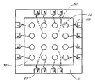
<도 1a>
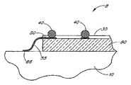
도 1a는 본 발명의 일 실시 형태에 따른, 확장 리드(expansion lead)를 사용하는 페이스-다운 팬-인 패키지(face-down, fan-in package)의 저면도.
<도 1b>
도 1b는 본 발명의 일 실시 형태에 따른, 확장 리드를 사용하는 페이스-다운 팬-인 패키지의 부분 단면도.
<도 1c>
도 1c는 본 발명의 일 실시 형태에 따른, 기판의 제2 표면 상에 리드들을 갖는, 확장 리드를 사용하는 페이스-다운 팬-인 패키지의 부분 단면도.
<도 1d>
도 1d는 본 발명의 일 실시 형태에 따른, 컴플라이언트 층(compliant layer)이 칩의 페이스 표면과 기판의 제1 표면 사이에 배치되는, 확장 리드를 사용하는 페이스-다운 팬-인 패키지의 부분 단면도.
<도 2>
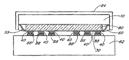
도 2는 μBGA 패키지의 사시도.
<도 3>
도 3은 μBGA 패키지의 단면도.
<도 4>
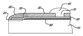
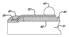
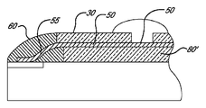
도 4는 본 발명의 바람직한 인터포저의 단면도.
<도 5>
도 5는 제2 레벨 패키지에 부착된 제1 레벨 패키지의 단면도.
<도 6>
도 6은 제1 레벨 패키지 케이스 없이 도시된 도 5의 제1 레벨 패키지의 단면도.Figure 1a
1A is a bottom view of a face-down fan-in package using expansion leads, in accordance with one embodiment of the present invention.
Figure 1b
1B is a partial cross-sectional view of a face-down fan-in package using an extension lead, in accordance with an embodiment of the invention.
Figure 1c
1C is a partial cross-sectional view of a face-down fan-in package using extension leads, having leads on a second surface of the substrate, in accordance with an embodiment of the present invention.
Figure 1d
1D is a partial cross-sectional view of a face-down fan-in package using extension leads, wherein a compliant layer is disposed between the face surface of the chip and the first surface of the substrate, in accordance with one embodiment of the present invention. .
2,
2 is a perspective view of a μBGA package.
3,
3 is a cross-sectional view of the μBGA package.
<Fig. 4>
4 is a cross-sectional view of a preferred interposer of the present invention.
5,
5 is a cross-sectional view of a first level package attached to a second level package.
6,
6 is a cross-sectional view of the first level package of FIG. 5 shown without a first level package case.
정의Justice
"전기 전도성 도메인"은 임의의 전도성 재료, 예를 들어 전도성 패드, 전도성 회로 또는 트레이스 등을 의미하고자 하는 것이다. 전기 전도성 도메인은 본 발명의 폴리이미드 필름에 의해 지지된다. 전기 전도성 도메인은 IC 칩과 IC 칩의 일부가 아닌 대상물(subject matter) 사이에 전기 전도성 계면을 적어도 일부 제공한다. 전기 전도성 계면은 i. IC 칩이 IC 칩의 일부가 아닌 대상물 (예를 들어, 인쇄 배선 보드 상의 회로, 입력/출력 소자 등)을 제어할 (또는 영향을 줄) 수 있게 하고/하거나; ii. IC 칩의 일부가 아닌 대상물 (예를 들어, IC 칩에 급전하기 위한 전기적 접속부)에 의해 IC 칩을 제어할 (또는 영향을 줄) 수 있게 한다."Electrically conductive domain" is intended to mean any conductive material, for example conductive pads, conductive circuits or traces and the like. The electrically conductive domains are supported by the polyimide film of the present invention. The electrically conductive domain provides at least a portion of the electrically conductive interface between the IC chip and a subject matter that is not part of the IC chip. The electrically conductive interface is i. Enable the IC chip to control (or affect) objects that are not part of the IC chip (eg, circuits on printed wiring boards, input / output elements, etc.); ii. It is possible to control (or affect) the IC chip by an object that is not part of the IC chip (for example, an electrical connection for feeding the IC chip).
"필름"은 자유 직립(free-standing) 필름 또는 (자가-지지(self-supporting) 또는 자가-비지지(non self-supporting)) 코팅을 의미하고자 하는 것이다. 용어 "필름"은 용어 "층"과 상호 교환적으로 사용되며 원하는 영역을 덮는 것을 말한다."Film" is intended to mean a free standing film or a coating (self-supporting or non self-supporting). The term "film" is used interchangeably with the term "layer" and refers to covering the desired area.
본 명세서에 사용되는 바와 같이, "2무수물"은 2무수물의 전구체 또는 유도체를 포함하고자 하는데, 이는 기술적으로는 2무수물일 수 없지만, 그럼에도 불구하고 이는 다이아민과 반응하여 폴리아믹산(polyamic acid) - 이어서, 이 폴리아믹산은 폴리이미드로 변환될 수 있음 - 을 형성하는 능력으로 인해 기능적으로 등가일 것이다.As used herein, "dihydride" is intended to include precursors or derivatives of dianhydride, which can not be technically an anhydride, but nevertheless it reacts with diamine to give polyamic acid- This polyamic acid will then be functionally equivalent due to its ability to form polyimide.
본 명세서에 사용되는 바와 같이, "다이아민"은 다이아민의 전구체 또는 유도체를 포함하고자 하는데, 이는 기술적으로는 다이아민일 수 없지만, 그럼에도 불구하고 이는 2무수물과 반응하여 폴리아믹산 - 이어서, 이 폴리아믹산은 폴리이미드로 변환될 수 있음 - 을 형성하는 능력으로 인해 기능적으로 등가이다.As used herein, "diamine" is intended to include precursors or derivatives of diamines, which technically cannot be diamines, but nevertheless it reacts with the dianhydride to form a polyamic acid-then this polyamic acid Functionally equivalent due to the ability to form-which can be converted to polyimide.
본 명세서에 사용되는 바와 같이, "폴리아믹산"은 2무수물 및 다이아민 단량체 또는 이들의 기능적 등가물의 조합으로부터 유도되고, 폴리이미드로 변환될 수 있는 임의의 폴리이미드 전구체 재료를 포함하고자 하는 것이다.As used herein, "polyamic acid" is intended to include any polyimide precursor material that is derived from a dianhydride and diamine monomer or a functional equivalent thereof and can be converted to a polyimide.
"서브마이크로미터"는 적어도 하나의 치수가 (수치 평균으로) 1 마이크로미터 미만인 입자를 기술하고자 하는 것이다."Submicrometer" is intended to describe particles having at least one dimension less than 1 micron (on a numerical average).
본 명세서에 사용되는 바와 같이, "화학 변환" 또는 "화학적으로 변환된"은 촉매(촉진제) 또는 탈수제 (또는 둘 모두)를 사용하여 폴리아믹산을 폴리이미드로 변환시키는 것을 나타내며, 이는 부분적으로 화학적으로 변환된 폴리이미드 - 이 폴리이미드는 이어서 승온에서 98% 초과의 고형물 수준으로 건조됨 - 를 포함하고자 하는 것이다.As used herein, "chemical conversion" or "chemically converted" refers to the conversion of polyamic acid to polyimide using a catalyst (promoter) or dehydrating agent (or both), which is partially chemically Converted polyimide, which polyimide is then dried to a solids level of greater than 98% at elevated temperature.
"종횡비"는 한 치수 대 다른 치수의 비, 예를 들어 길이 대 높이의 비를 의미하고자 하는 것이다."Aspect ratio" is intended to mean the ratio of one dimension to another, for example the ratio of length to height.
소정의 중합체의 설명에 있어서, 때때로 출원인들은 중합체를 제조하기 위해 사용되는 단량체 또는 중합체를 제조하기 위해 사용되는 단량체의 양에 의해 그 중합체를 언급하는 것으로 이해되어야 한다. 그러한 설명은 최종 중합체를 설명하기 위해 사용되는 특정 명명법을 포함하지 않을 수 있거나 또는 제법 한정 물건(product-by-process) 용어를 포함하지 않을 수 있지만, 단량체 및 양에 대한 임의의 그러한 언급은 그 내용이 달리 나타내지 않거나 함축하지 않는다면 중합체가 그러한 단량체로부터 제조됨을 의미하는 것으로 해석되어야 한다.In the description of a given polymer, it is sometimes understood that applicants refer to the polymer by the amount of monomer used to make the polymer or the monomer used to make the polymer. Such descriptions may not include the specific nomenclature used to describe the final polymer or may not include product-by-process terminology, but any such reference to monomers and amounts is intended to Unless otherwise indicated or implied, it should be interpreted to mean that the polymer is prepared from such monomers.
본 명세서에 사용되는 바와 같이, 용어 "포함하다", "포함하는", "함유하다", "함유하는", "갖다", "갖는" 또는 이들의 임의의 다른 변형은 배타적이지 않은 포함을 커버하고자 하는 것이다. 예를 들어, 요소들의 목록을 포함하는 방법, 공정, 물품 또는 장치는 반드시 그러한 요소만으로 제한되지는 않고, 그러한 방법, 공정, 물품 또는 장치에 대해 명확하게 열거되지 않거나 내재적인 다른 요소를 포함할 수 있다. 또한, 명백히 반대로 기술되지 않는다면, "또는"은 포괄적인 '또는'을 말하며 배타적인 '또는'을 말하는 것은 아니다. 예를 들어, 조건 A 또는 B는 하기 중 어느 하나에 의해 만족된다: A는 참(또는 존재함)이고 B는 거짓(또는 존재하지 않음), A는 거짓(또는 존재하지 않음)이고 B는 참(또는 존재함), 그리고 A 및 B 모두가 참(또는 존재함).As used herein, the terms “comprises”, “comprising”, “comprises”, “comprising”, “have”, “having” or any other variations thereof cover a non-exclusive inclusion. I would like to. For example, a method, process, article, or apparatus that includes a list of elements is not necessarily limited to such elements, and may include other elements that are not explicitly listed or inherent to such method, process, article, or apparatus. have. Also, unless expressly stated to the contrary, "or" refers to an inclusive 'or' and not an exclusive 'or'. For example, condition A or B is satisfied by any of the following: A is true (or present) and B is false (or not present), A is false (or not present) and B is true (Or present), and both A and B are true (or present).
또한, 부정관사("a" 또는 "an")가 본 발명의 요소들 및 구성요소들을 설명하는 데 이용된다. 이는 단지 편의상 그리고 본 발명의 전반적인 의미를 제공하기 위해 행해진다. 이러한 표현은 하나 또는 적어도 하나를 포함하는 것으로 파악되어야 하며, 단수형은 그 수가 명백하게 단수임을 의미하는 것이 아니라면 복수형을 또한 포함한다.Also, indefinite articles "a" or "an" are used to describe elements and components of the present invention. This is done merely for convenience and to give a general sense of the invention. Such expressions should be understood to include one or at least one, and the singular also includes the plural unless the number is obviously meant to be singular.
개요summary
본 발명의 인터포저 필름은 기판에 의해 지지되는 복수의 전기 전도성 도메인들을 갖는다. 본 발명의 기판은 폴리이미드와 서브마이크로미터 충전제를 포함한다. 본 발명의 서브마이크로미터 충전제는 일반적으로 열팽창 계수를 유지하거나 감소시키고 저장 탄성률을 증가시키면서 기판이 과도하게 취성이 되게 하지 않고서 상대적으로 높은 로딩률(loading)로 기판 내로 혼입될 수 있다. 폴리이미드는 강성 로드 부분 및 비강성 로드 부분을 포함하는 하이브리드 골격 구조를 갖는다. 본 발명의 인터포저 필름은 롤-투-롤(roll-to-roll) 가공 또는 릴-투-릴 가공에서 인터포저 필름을 이용하는 임의의 IC 패키징 기술에 적합하다.The interposer film of the present invention has a plurality of electrically conductive domains supported by a substrate. Substrates of the invention include polyimide and submicron fillers. Submicrometer fillers of the present invention can generally be incorporated into a substrate at relatively high loadings without maintaining the substrate's coefficient of thermal expansion and increasing its storage modulus without making the substrate excessively brittle. The polyimide has a hybrid backbone structure that includes a rigid rod portion and a non-rigid rod portion. The interposer film of the present invention is suitable for any IC packaging technology that uses an interposer film in roll-to-roll processing or reel to reel processing.
폴리이미드Polyimide
본 발명의 폴리이미드는 소정 방향족 2무수물과 소정 방향족 다이아민의 중합 반응으로부터 유도되어 강성 로드 부분 및 비강성 로드 부분 둘 모두를 포함하는 중합체 골격 구조를 제공한다. 강성 로드 부분은 폴리이미드로의 방향족 강성 로드 단량체의 중합으로부터 생기고, 비강성 로드 부분은 폴리이미드로의 방향족 비강성 로드 단량체의 중합으로부터 생긴다. 방향족 강성 로드 단량체는 중합체 골격에 대해 동일선상(co-linear; 약 180°) 배치를 제공하며, 따라서 폴리이미드로 중합될 때 상대적으로 적은 운동 가능성을 제공한다.The polyimide of the present invention is derived from the polymerization of certain aromatic dianhydrides with certain aromatic diamines to provide a polymer backbone structure comprising both rigid rod portions and non-rigid rod portions. The rigid rod portion results from the polymerization of the aromatic rigid rod monomer to the polyimide, and the non-rigid rod portion results from the polymerization of the aromatic non-rigid rod monomer to the polyimide. Aromatic rigid rod monomers provide a co-linear arrangement with respect to the polymer backbone, thus providing a relatively low mobility when polymerized with polyimide.
방향족 강성 로드 다이아민 단량체의 예는 다음과 같다:Examples of aromatic rigid rod diamine monomers are as follows:
1,4-다이아미노벤젠 (PPD),1,4-diaminobenzene (PPD),
4,4'-다이아미노바이페닐,4,4'-diaminobiphenyl,
2,2'-비스(트라이플루오로메틸) 4,4'-다이아미노바이페닐 (TFMB),2,2'-bis (trifluoromethyl) 4,4'-diaminobiphenyl (TFMB),
1,4-나프탈렌다이아민,1,4-naphthalenediamine,
1,5-나프탈렌다이아민,1,5-naphthalenediamine,
4,4"-다이아미노 터페닐,4,4 "-diamino terphenyl,
4,4'-다이아미노 벤즈아닐리드,4,4'-diamino benzanilide,
4,4'-다이아미노페닐 벤조에이트,4,4'-diaminophenyl benzoate,
3,3'-다이메틸-4,4'-다이아미노바이페닐,3,3'-dimethyl-4,4'-diaminobiphenyl,
2,5-다이아미노톨루엔2,5-diaminotoluene
등.Etc.
방향족 강성 로드 2무수물 단량체의 예는 다음과 같다:Examples of aromatic rigid rod dianhydride monomers are as follows:
파이로멜리트산 2무수물 (PMDA),Pyromellitic dianhydride (PMDA),
2,3,6,7-나프탈렌테트라카르복실산 2무수물, 및2,3,6,7-naphthalenetetracarboxylic dianhydride, and
3,3',4,4'-바이페닐 테트라카르복실산 2무수물 (BPDA).3,3 ', 4,4'-biphenyl tetracarboxylic dianhydride (BPDA).
(일단 폴리이미드로 중합되면) (강성 로드 다이아민 및 강성 로드 2무수물의) 상기 예와 실질적으로 같거나 또는 그 미만인 회전 운동 또는 굽힘의 자유도(freedom)를 갖는 단량체는 본 발명의 목적을 위한 강성 로드 단량체인 것으로 여기고자 하는 것이다.Monomers having a degree of freedom of rotational motion or bending that are substantially equal to or less than the above examples (once polymerized with polyimide) (of rigid rod diamines and rigid rod dianhydrides) are intended for the purposes of the present invention. It is intended to be considered to be a rigid rod monomer.
본 발명의 목적을 위한 비강성 로드 단량체는 상기에 기재되고 예시된 강성 로드 단량체와 비교하여 실질적으로 더 큰 운동 자유도를 갖는 폴리이미드 골격 구조로 중합될 수 있는 방향족 단량체를 의미하고자 하는 것이다. 비강성 로드 단량체는, 폴리이미드로 중합될 때, 굽힘을 갖는 골격 구조를 제공하거나 아니면 이들이 생성하는 폴리이미드 골격을 따라 동일선상이 아니다 (즉, 약 180°가 아니다). 본 발명에 따른 비강성 로드 단량체의 예에는 폴리이미드 골격을 따라 회전 또는 굽힘 가교기(bridging group)를 제공할 수 있는 임의의 다이아민 및 임의의 2무수물이 포함된다. 회전 또는 굽힘 가교기의 예에는 -O-, -S-, -SO2-, -C(O)-, -C(CH3) 2-, -C(CF3) 2-, 및 -C(R,R')- (여기서, R 및 R'는 동일하거나 상이하며, 탄소에 결합할 수 있는 임의의 유기 기임)이 포함된다.Non-rigid rod monomers for the purposes of the present invention are intended to mean aromatic monomers which can be polymerized into a polyimide backbone structure having substantially greater freedom of movement compared to the rigid rod monomers described and illustrated above. Non-rigid rod monomers, when polymerized with polyimide, provide a skeletal structure with bending or are not collinear along the polyimide backbone they produce (ie, not about 180 °). Examples of non-rigid rod monomers according to the present invention include any diamine and any dianhydride capable of providing a rotating or bending bridging group along the polyimide backbone. Examples of rotating or bending crosslinkers include -O-, -S-, -SO 2- , -C (O)-, -C (CH 3 ) 2- , -C (CF 3 ) 2- , and -C ( R, R ')-, wherein R and R' are the same or different and are any organic group capable of bonding to carbon.
비강성 로드 다이아민의 예에는 4,4'-다이아미노다이페닐 에테르 ("ODA"), 2,2-비스-(4-아미노페닐) 프로판, 1,3-다이아미노벤젠 (MPD), 4,4'-다이아미노벤조페논, 4,4'-다이아미노다이페닐메탄, 4,4'-다이아미노다이페닐 설파이드, 4,4'-다이아미노다이페닐 설폰, 3,3'-다이아미노다이페닐 설폰, 비스-(4-(4-아미노페녹시)페닐 설폰 (BAPS), 4,4'-비스-(아미노페녹시)바이페닐 (BAPB), 3,4'-다이아미노다이페닐 에테르, 4,4'-다이아미노벤조페논, 4,4'-아이소프로필리덴다이아닐린, 2,2'-비스-(3-아미노페닐)프로판, N,N-비스-(4-아미노페닐)-n-부틸아민, N,N-비스-(4-아미노페닐) 메틸아민, m-아미노 벤조일-p-아미노 아닐리드, 4-아미노페닐-3-아미노벤조에이트, N,N-비스-(4-아미노페닐) 아닐린, 2,4-다이아미노톨루엔, 2,6-다이아미노톨루엔, 2,4-다이아민-5-클로로톨루엔, 2,4-다이아미노-6-클로로톨루엔, 2,4-비스-(베타-아미노-t-부틸) 톨루엔, 비스-(p-베타-아미노-t-부틸 페닐) 에테르, p-비스-2-(2-메틸-4-아미노펜틸) 벤젠, m-자일릴렌 다이아민, p-자일릴렌 다이아민, 1,2-비스-(4-아미노페녹시)벤젠, 1,3-비스-(4-아미노페녹시) 벤젠, 1,2-비스-(3-아미노페녹시)벤젠, 1,3-비스-(3-아미노페녹시) 벤젠, 1-(4-아미노페녹시)-3-(3-아미노페녹시) 벤젠, 1,4-비스-(4-아미노페녹시) 벤젠, 1,4-비스-(3-아미노페녹시) 벤젠, 1-(4-아미노페녹시)-4-(3-아미노페녹시) 벤젠, 2,2-비스-(4-[4-아미노페녹시]페닐) 프로판 (BAPP), 2,2'-비스-(4-아미노페닐)-헥사플루오로 프로판 (6F 다이아민), 2,2'-비스-(4-페녹시 아닐린) 아이소프로필리덴, 4,4'-다이아미노-2,2'-트라이플루오로메틸 다이페닐옥사이드, 3,3'-다이아미노-5,5'-트라이플루오로메틸 다이페닐옥사이드, 4,4'-트라이플루오로메틸-2,2'-다이아미노바이페닐, 2,4,6-트라이메틸-1,3-다이아미노벤젠, 4,4'-옥시-비스-[2-트라이플루오로메틸)벤젠 아민] (1,2,4-OBABTF), 4,4'-옥시-비스-[3-트라이플루오로메틸)벤젠 아민], 4,4'-티오-비스-[(2-트라이플루오로메틸)벤젠-아민], 4,4'-티오비스[(3-트라이플루오로메틸)벤젠 아민], 4,4'-설폭실-비스-[(2-트라이플루오로메틸)벤젠 아민, 4,4'-설폭실-비스-[(3-트라이플루오로메틸)벤젠 아민], 및 4,4'-케토-비스-[(2-트라이플루오로메틸)벤젠 아민]이 포함된다.Examples of non-rigid rod diamines include 4,4'-diaminodiphenyl ether ("ODA"), 2,2-bis- (4-aminophenyl) propane, 1,3-diaminobenzene (MPD), 4, 4'-diaminobenzophenone, 4,4'-diaminodiphenylmethane, 4,4'-diaminodiphenyl sulfide, 4,4'-diaminodiphenyl sulfone, 3,3'-diaminodiphenyl Sulfone, bis- (4- (4-aminophenoxy) phenyl sulfone (BAPS), 4,4'-bis- (aminophenoxy) biphenyl (BAPB), 3,4'-diaminodiphenyl ether, 4 , 4'-diaminobenzophenone, 4,4'-isopropylidenedianiline, 2,2'-bis- (3-aminophenyl) propane, N, N-bis- (4-aminophenyl) -n- Butylamine, N, N-bis- (4-aminophenyl) methylamine, m-amino benzoyl-p-amino anilide, 4-aminophenyl-3-aminobenzoate, N, N-bis- (4-aminophenyl ) Aniline, 2,4-diaminotoluene, 2,6-diaminotoluene, 2,4-diamine-5-chlorotoluene, 2,4-diamino-6-cle Rotoluene, 2,4-bis- (beta-amino-t-butyl) toluene, bis- (p-beta-amino-t-butyl phenyl) ether, p-bis-2- (2-methyl-4-aminophen Butyl) benzene, m-xylylene diamine, p-xylylene diamine, 1,2-bis- (4-aminophenoxy) benzene, 1,3-bis- (4-aminophenoxy) benzene, 1, 2-bis- (3-aminophenoxy) benzene, 1,3-bis- (3-aminophenoxy) benzene, 1- (4-aminophenoxy) -3- (3-aminophenoxy) benzene, 1 , 4-bis- (4-aminophenoxy) benzene, 1,4-bis- (3-aminophenoxy) benzene, 1- (4-aminophenoxy) -4- (3-aminophenoxy) benzene, 2,2-bis- (4- [4-aminophenoxy] phenyl) propane (BAPP), 2,2'-bis- (4-aminophenyl) -hexafluoro propane (6F diamine), 2,2 '-Bis- (4-phenoxy aniline) isopropylidene, 4,4'-diamino-2,2'-trifluoromethyl diphenyloxide, 3,3'-diamino-5,5'-tri Fluoromethyl diphenyloxide, 4,4'-trifluoromethyl-2,2'-da Aminobiphenyl, 2,4,6-trimethyl-1,3-diaminobenzene, 4,4'-oxy-bis- [2-trifluoromethyl) benzene amine] (1,2,4-OBABTF) , 4,4'-oxy-bis- [3-trifluoromethyl) benzene amine], 4,4'-thio-bis-[(2-trifluoromethyl) benzene-amine], 4,4'- Thiobis [(3-trifluoromethyl) benzene amine], 4,4'-suloxyl-bis-[(2-trifluoromethyl) benzene amine, 4,4'-suloxyl-bis-[(3 -Trifluoromethyl) benzene amine], and 4,4'-keto-bis-[(2-trifluoromethyl) benzene amine].
방향족 비강성 로드 2무수물의 예에는 2,2',3,3'-벤조페논 테트라카르복실산 2무수물, 2,3,3',4'-벤조페논 테트라카르복실산 2무수물, 3,3',4,4'-벤조페논 테트라카르복실산 2무수물 (BTDA), 2,2',3,3'-바이페닐 테트라카르복실산 2무수물, 2,3,3',4'-바이페닐 테트라카르복실산 2무수물, 4,4'-티오-다이프탈산 무수물, 비스 (3,4-다이카르복시페닐) 설폰 2무수물 (DSDA), 비스 (3,4-다이카르복시페닐) 설폭사이드 2무수물, 4,4'-옥시다이프탈산 무수물 (ODPA), 비스 (3,4-다이카르복시페닐) 티오 에테르 2무수물, 2,2-비스[4-(3,4-다이카르복시페녹시)페닐]프로판 2무수물 (BPADA), 비스페놀 S 2무수물, 2,2-비스-(3,4-다이카르복시페닐) 1,1,1,3,3,3,-헥사플루오로프로판 2무수물 (6FDA), 5,5-[2,2,2]-트라이플루오로-1-(트라이플루오로메틸)에틸리덴, 비스-1,3-아이소벤조푸란다이온, 비스 (3,4-다이카르복시페닐) 메탄 2무수물, 사이클로펜타다이에닐 테트라카르복실산 2무수물, 에틸렌 테트라카르복실산 2무수물, 2,2-비스(3,4-다이카르복시페닐) 프로판 2무수물이 포함된다.Examples of aromatic non-rigid rod dianhydrides include 2,2 ', 3,3'-benzophenone tetracarboxylic dianhydride, 2,3,3', 4'-benzophenone tetracarboxylic dianhydride, 3,3 ', 4,4'-benzophenone tetracarboxylic dianhydride (BTDA), 2,2', 3,3'-biphenyl tetracarboxylic dianhydride, 2,3,3 ', 4'-biphenyl Tetracarboxylic dianhydride, 4,4'-thio-diphthalic anhydride, bis (3,4-dicarboxyphenyl) sulfone dianhydride (DSDA), bis (3,4-dicarboxyphenyl) sulfoxide dianhydride, 4,4'-oxydiphthalic anhydride (ODPA), bis (3,4-dicarboxyphenyl) thio ether dianhydride, 2,2-bis [4- (3,4-dicarboxyphenoxy) phenyl] propane 2 Anhydride (BPADA), bisphenol S 2 anhydride, 2,2-bis- (3,4-dicarboxyphenyl) 1,1,1,3,3,3, -hexafluoropropane dianhydride (6FDA), 5, 5- [2,2,2] -trifluoro-1- (trifluoromethyl) ethylidene, bis-1,3-isobenzofurandione, bis (3,4-dicarboxy Ciphenyl) methane dianhydride, cyclopentadienyl tetracarboxylic dianhydride, ethylene tetracarboxylic dianhydride, 2,2-bis (3,4-dicarboxyphenyl) propane dianhydride.
일부 실시 형태에서, 2무수물 대 다이아민의 몰비는 (48-52):(52-48)이고, X:Y의 비는 (20-80):(80-20)이며, 여기서 폴리이미드의 총 2무수물 성분 및 다이아민 성분을 기준으로 X는 강성 로드 2무수물과 강성 로드 다이아민의 몰%이고 Y는 비강성 로드 2무수물과 비강성 로드 다이아민의 몰%이다. 그리고 대안적인 실시 형태에서, 그러한 광범위한 비 내에 임의의 하위 범위가 있을 수 있다 (예를 들어, 20 내지 80에는 20, 25, 30, 35, 40, 45, 50, 55, 60, 65, 70, 75와 80 사이의 그리고 선택적으로 이들을 포함하는 임의의 범위가 포함되고, 80 내지 20에는 80, 75, 70, 65, 60, 55, 45, 40, 35, 30과 25 사이의 그리고 선택적으로 이들을 포함하는 임의의 범위가 포함된다).In some embodiments, the molar ratio of dianhydride to diamine is (48-52) :( 52-48) and the ratio of X: Y is (20-80) :( 80-20), wherein the total of polyimide is 2 Based on the anhydride component and the diamine component, X is the mole percent of the rigid rod dianhydride and the rigid rod diamine and Y is the mole percent of the non-rigid rod dianhydride and the non-rigid rod diamine. And in alternative embodiments, there may be any subrange within such a wide range of ratios (eg, 20 to 80 at 20, 25, 30, 35, 40, 45, 50, 55, 60, 65, 70, Any range between 75 and 80 and optionally including them, 80 to 20 includes between 80, 75, 70, 65, 60, 55, 45, 40, 35, 30 and 25 and optionally these Arbitrary ranges are included).
일 실시 형태에서, 본 발명의 폴리이미드는 실질적으로 등몰량의 4,4'-다이아미노다이페닐 에테르 (4,4'-ODA) 비강성 로드 단량체, 및 파이로멜리트산 2무수물 (PMDA) 강성 로드 단량체로부터 유도된다. 다른 실시 형태에서, 방향족 2무수물 성분의 70 몰% 이상은 파이로멜리트산 2무수물이고; 방향족 다이아민 성분의 70 몰% 이상은 4,4'-다이아미노다이페닐 에테르이다. 일부 실시 형태에서, (폴리이미드의 총 2무수물 함량을 기준으로) 방향족 2무수물 성분의 70, 75, 80, 85, 90 또는 95 몰% 이상은 파이로멜리트산 2무수물이고; (폴리이미드의 총 다이아민 함량을 기준으로) 방향족 다이아민 성분의 70, 75, 80, 85, 90 또는 95 몰% 이상은 4,4'-다이아미노다이페닐 에테르이다. 그러한 PMDA//4,4'ODA 폴리이미드는 상대적으로 저가에서의 개선된 특성을 위한 본 발명의 서브마이크로미터 충전제와의 배합에 특히 잘 적합한 것으로 밝혀졌다. 다른 실시 형태에서, 폴리이미드는 100 몰%의 파이로멜리트산 2무수물 및 100 몰%의 4,4'-다이아미노다이페닐 에테르로부터 유도된다. 다른 실시 형태에서, 폴리이미드는 4,4'-다이아미노다이페닐 에테르 및 1,4 다이아미노벤젠과 파이로멜리트산 2무수물 및 3,3',4,4'-바이페닐 테트라카르복실산 2무수물로부터 유도되는 랜덤 공중합체이다. 또 다른 실시 형태에서, 폴리이미드는 4,4'-다이아미노다이페닐 에테르 및 1,4 다이아미노벤젠과 파이로멜리트산 2무수물로부터 유도되는 랜덤 공중합체이다.In one embodiment, the polyimides of the present invention are substantially equimolar amounts of 4,4'-diaminodiphenyl ether (4,4'-ODA) non-rigid rod monomers, and pyromellitic dianhydride (PMDA) stiffness Derived from the rod monomer. In another embodiment, at least 70 mole% of the aromatic dianhydride component is pyromellitic dianhydride; At least 70 mole% of the aromatic diamine component is 4,4'-diaminodiphenyl ether. In some embodiments, at least 70, 75, 80, 85, 90, or 95 mole percent of the aromatic dianhydride component (based on the total dianhydride content of the polyimide) is pyromellitic dianhydride; At least 70, 75, 80, 85, 90 or 95 mole percent of the aromatic diamine component (based on the total diamine content of the polyimide) is 4,4'-diaminodiphenyl ether. Such PMDA // 4,4'ODA polyimides have been found to be particularly well suited for blending with submicrometer fillers of the present invention for improved properties at relatively low cost. In another embodiment, the polyimide is derived from 100 mol% pyromellitic dianhydride and 100 mol% 4,4′-diaminodiphenyl ether. In another embodiment, the polyimide is 4,4'-diaminodiphenyl ether and 1,4 diaminobenzene and pyromellitic dianhydride and 3,3 ', 4,4'-biphenyl tetracarboxylic acid 2 It is a random copolymer derived from anhydrides. In another embodiment, the polyimide is a 4,4'-diaminodiphenyl ether and a random copolymer derived from 1,4 diaminobenzene and pyromellitic dianhydride.
다른 실시 형태에서, 방향족 2무수물의 75 몰% 이상은 파이로멜리트산 2무수물이고, 방향족 다이아민 성분으로서 70 몰%는 4,4'-다이아미노다이페닐 에테르이고 30 몰%는 1,4 다이아미노벤젠이다.In another embodiment, at least 75 mol% of the aromatic dianhydride is pyromellitic dianhydride, 70 mol% as the aromatic diamine component is 4,4′-diaminodiphenyl ether and 30 mol% is 1,4 di Aminobenzene.
다른 실시 형태에서, 폴리이미드는 블록 공중합체이다. 블록 공중합체는 단량체 배열(sequence)들의 완전히 랜덤한 분포와 대조적으로 중합체 골격을 따라 실질적으로 하나인 2무수물/다이아민 조합의 배열들이 있는 중합체이다. 전형적으로, 이는 폴리아믹산 제조 동안 상이한 단량체들의 축차 부가에 의해 달성된다.In another embodiment, the polyimide is a block copolymer. Block copolymers are polymers with arrays of substantially one dianhydride / diamine combination along the polymer backbone as opposed to a completely random distribution of monomer sequences. Typically this is achieved by the sequential addition of different monomers during polyamic acid production.
또 다른 실시 형태에서, 폴리이미드는 4,4'-다이아미노다이페닐 에테르 및 1,4-다이아미노벤젠과 파이로멜리트산 2무수물로부터 유도되는 블록 공중합체이다. 또 다른 실시 형태에서, 폴리이미드는 4,4'-다이아미노다이페닐 에테르 (4,4'-ODA) 및 1,4-다이아미노벤젠 (PPD)과 파이로멜리트산 2무수물 (PMDA) 및 3,3',4,4'-바이페닐 테트라카르복실산 2무수물 (BPDA)로부터 유도되는 블록 공중합체이다. 또 다른 실시 형태에서, 폴리이미드는 실질적으로 강성인 블록 (PPD와 반응된 PMDA)과 실질적으로 더 연성인 블록 (ODA와 반응된 PMDA)으로 이루어진 블록 공중합체이다. 다른 실시 형태에서, 블록 공중합체는 10 내지 40 몰%의 파이로멜리트산 2무수물 및 1,4-다이아미노벤젠의 블록과 90 내지 60 몰%의 파이로멜리트산 2무수물 및 4,4'-다이아미노다이페닐 에테르의 블록으로부터 유도된다.In another embodiment, the polyimide is a 4,4'-diaminodiphenyl ether and a block copolymer derived from 1,4-diaminobenzene and pyromellitic dianhydride. In another embodiment, the polyimide is 4,4'-diaminodiphenyl ether (4,4'-ODA) and 1,4-diaminobenzene (PPD) and pyromellitic dianhydride (PMDA) and 3 Block copolymers derived from, 3 ', 4,4'-biphenyl tetracarboxylic dianhydride (BPDA). In yet another embodiment, the polyimide is a block copolymer consisting of substantially rigid blocks (PMDA reacted with PPD) and substantially softer blocks (PMDA reacted with ODA). In another embodiment, the block copolymer comprises 10-40 mole% of pyromellitic dianhydride and 1,4-diaminobenzene and 90-60 mole% of pyromellitic dianhydride and 4,4'- Derived from a block of diaminodiphenyl ether.
서브마이크로미터 충전제Submicrometer filler
본 발명에 따르면, 충전제는 (적어도 하나의 치수에 있어서) 서브마이크로미터 충전제 또는 서브마이크로미터 충전제들의 혼합물이다.According to the invention, the filler is (in at least one dimension) a submicrometer filler or a mixture of submicrometer fillers.
일 실시 형태에서, 본 발명의 폴리이미드 필름은 적어도 하나의 서브마이크로미터 충전제를 포함하며, 상기 서브마이크로미터 충전제는In one embodiment, the polyimide film of the invention comprises at least one submicron filler, the submicron filler
1. 적어도 하나의 치수가 550 나노미터 미만 (그리고 일부 실시 형태에서는, 475, 450, 425, 400, 375, 350, 325, 300, 275, 250, 225 또는 200 나노미터 미만)이고 (충전제가 임의의 치수에 있어서 다양한 형상을 가질 수 있기 때문에 그리고 충전제 형상이 임의의 치수를 따라 변할 수 있기 때문에, "적어도 하나의 치수"는 그 치수를 따른 수치 평균이고자 함);1. At least one dimension is less than 550 nanometers (and in some embodiments, less than 475, 450, 425, 400, 375, 350, 325, 300, 275, 250, 225 or 200 nanometers) and the filler is optional "At least one dimension" is intended to be a numerical average along that dimension, since it may have various shapes in the dimensions of and since the filler shape may vary along any dimension;
2. 평균 종횡비가 3:1, 4:1, 5:1, 6:1, 7:1, 8:1, 9:1, 10:1, 11:1, 12:1, 13:1, 14:1 또는 15:1 초과이고;2. The average aspect ratio is 3: 1, 4: 1, 5: 1, 6: 1, 7: 1, 8: 1, 9: 1, 10: 1, 11: 1, 12: 1, 13: 1, 14 : 1 or greater than 15: 1;
3. 모든 치수가 기판 두께의 100%, 95%, 90%, 85%, 80%, 75%, 70%, 65%, 60%, 55%, 50%, 45%, 40%, 35%, 30%, 25%, 20%, 15% 또는 10% 미만이고;3. All dimensions are 100%, 95%, 90%, 85%, 80%, 75%, 70%, 65%, 60%, 55%, 50%, 45%, 40%, 35% of substrate thickness, Less than 30%, 25%, 20%, 15% or 10%;
4. 기판의 10, 15, 20, 25, 30, 35, 40 및 45 부피%의 백분율 중 임의의 둘 사이의 그리고 선택적으로 이들 둘을 포함하는 양으로 존재한다.4. It is present in an amount between any two of the percentages of 10, 15, 20, 25, 30, 35, 40 and 45% by volume of the substrate and optionally including both.
적합한 서브마이크로미터 충전제는 일반적으로 300, 350, 400, 425 또는 450℃보다 높은 온도에서 안정하며, 일부 실시 형태에서는 기판의 전기 절연 특성을 유의하게 감소시키지 않는다. 일부 실시 형태에서, 서브마이크로미터 충전제는 바늘형(needle-like) 충전제 (침상(acicular) 충전제), 섬유상 충전제, 소판형(platelet) 충전제 및 그 혼합물로 이루어진 군으로부터 선택된다. 일 실시 형태에서, 서브마이크로미터 충전제는 실질적으로 응집되지 않는다. 서브마이크로미터 충전제는 중공, 다공성 또는 중실일 수 있다.Suitable submicron fillers are generally stable at temperatures above 300, 350, 400, 425 or 450 ° C. and in some embodiments do not significantly reduce the electrical insulation properties of the substrate. In some embodiments, the submicrometer filler is selected from the group consisting of needle-like fillers (acicular fillers), fibrous fillers, platelet fillers, and mixtures thereof. In one embodiment, the submicron fillers are not substantially aggregated. Submicron fillers can be hollow, porous or solid.
일 실시 형태에서, 본 발명의 서브마이크로미터 충전제는 3:1, 4:1, 5:1, 6:1, 7:1, 8:1, 9:1, 10:1, 11:1, 12:1, 13:1, 14:1 또는 15:1 이상의 종횡비를 나타낸다. 일 실시 형태에서, 서브마이크로미터 충전제의 종횡비는 5:1 이상이다. 다른 실시 형태에서 서브마이크로미터 충전제의 종횡비는 10:1 이상이며, 다른 실시 형태에서 종횡비는 12:1 이상이다. 일부 실시 형태에서, 서브마이크로미터 충전제는 산화물(예를 들어, 규소, 마그네슘 및/또는 알루미늄을 포함하는 산화물), 질화물(예를 들어, 붕소 및/또는 규소를 포함하는 질화물), 탄화물(예를 들어, 텅스텐 및/또는 규소를 포함하는 탄화물) 및 그 조합으로 이루어진 군으로부터 선택된다. 일부 실시 형태에서, 서브마이크로미터 충전제는 침상 이산화티타늄, 활석, SiC 섬유, 판상(platy) Al2O3 또는 그 혼합물이다. 일부 실시 형태에서, 서브마이크로미터 충전제는 모든 치수가 (수치 평균으로) 50, 25, 20, 15, 12, 10, 8, 6, 5, 4 또는 2 마이크로미터 미만이다.In one embodiment, the submicrometer filler of the invention is 3: 1, 4: 1, 5: 1, 6: 1, 7: 1, 8: 1, 9: 1, 10: 1, 11: 1, 12 An aspect ratio of at least 1: 1, 13: 1, 14: 1, or 15: 1. In one embodiment, the aspect ratio of the submicron filler is at least 5: 1. In another embodiment the aspect ratio of the submicron filler is at least 10: 1, and in other embodiments the aspect ratio is at least 12: 1. In some embodiments, submicrometer fillers include oxides (eg, oxides including silicon, magnesium, and / or aluminum), nitrides (eg, nitrides including boron and / or silicon), carbides (eg, Carbides comprising tungsten and / or silicon) and combinations thereof. In some embodiments, the submicron filler is acicular titanium dioxide, talc, SiC fibers, plated Al 2 O 3 or mixtures thereof. In some embodiments, the submicron filler has all dimensions less than 50, 25, 20, 15, 12, 10, 8, 6, 5, 4, or 2 micrometers (on a numerical average).
또 다른 실시 형태에서, 기계적 특성을 증가시키기 위해서 탄소 섬유 및 흑연이 다른 서브마이크로미터 충전제와 조합하여 사용될 수 있다. 그러나 일 실시 형태에서, 흑연, 탄소 섬유 및/또는 전기 전도성 충전제의 로딩률(loading)은 퍼콜레이션 문턱값(percolation threshold) 미만 (아마도 10 부피% 미만)일 필요가 있을 수 있는데, 이는 흑연 및 탄소 섬유 충전제가 전기 절연 특성을 감소시킬 수 있으며 일부 실시 형태에서는 감소된 전기 절연 특성이 바람직하지 않기 때문이다.In another embodiment, carbon fibers and graphite may be used in combination with other submicron fillers to increase mechanical properties. However, in one embodiment, the loading of graphite, carbon fiber and / or electrically conductive filler may need to be below the percolation threshold (possibly less than 10% by volume), which is graphite and carbon This is because fiber fillers can reduce electrical insulation properties and in some embodiments reduced electrical insulation properties are undesirable.
일부 실시 형태에서, 서브마이크로미터 충전제는 커플링제로 코팅된다. 일부 실시 형태에서, 서브마이크로미터 충전제는 아미노실란 커플링제로 코팅된다. 일부 실시 형태에서, 서브마이크로미터 충전제는 분산제로 코팅된다. 일부 실시 형태에서, 서브마이크로미터 충전제는 커플링제와 분산제의 조합으로 코팅된다. 일부 실시 형태에서, 서브마이크로미터 충전제는 커플링제, 분산제 또는 그 조합으로 코팅된다. 대안적으로, 커플링제 및/또는 분산제는 필름 내로 직접 혼입될 수 있으며, 반드시 서브마이크로미터 충전제 상에 코팅되는 것은 아니다. 일부 실시 형태에서, 서브마이크로미터 충전제는 적어도 일부가 산화알루미늄으로 코팅된 침상 이산화티타늄을 포함한다.In some embodiments, the submicrometer filler is coated with a coupling agent. In some embodiments, the submicrometer filler is coated with an aminosilane coupling agent. In some embodiments, the submicrometer filler is coated with a dispersant. In some embodiments, the submicrometer filler is coated with a combination of coupling agent and dispersant. In some embodiments, the submicrometer filler is coated with a coupling agent, a dispersant, or a combination thereof. Alternatively, coupling agents and / or dispersants may be incorporated directly into the film and are not necessarily coated on submicrometer fillers. In some embodiments, the submicrometer filler comprises acicular titanium dioxide at least partially coated with aluminum oxide.
일부 실시 형태에서, 서브마이크로미터 충전제는 원하는 가공 온도에서 그 자체가 열화되거나 또는 배출가스(off-gas)를 생성하지 않도록 선택된다. 마찬가지로 일부 실시 형태에서, 서브마이크로미터 충전제는 중합체 열화에 기여하지 않도록 선택된다.In some embodiments, the submicrometer filler is selected such that it does not degrade itself or produce off-gas at the desired processing temperature. Likewise in some embodiments, the submicron filler is chosen so as not to contribute to polymer degradation.
일 실시 형태에서, 충전제 복합체(예를 들어, 단일 또는 다수의 코어/쉘 구조체)가 사용될 수 있으며, 여기서 하나의 산화물은 하나의 입자에서 다른 산화물을 캡슐화한다.In one embodiment, filler composites (eg, single or multiple core / shell structures) can be used, where one oxide encapsulates another oxide in one particle.
기판Board
상대적으로 덜 고가인 폴리이미드가 본 발명의 서브마이크로미터 충전제로 충전될 수 있고, 그럼으로써 적어도 여러가지 점에서 더 고가인 폴리이미드와 더 유사하게 그러나 훨씬 더 낮은 비용으로 기능할 수 있음이 밝혀졌다. 더 고가인 단량체, 예를 들어 BPDA 또는 플루오르화 단량체는 덜 고가인 단량체로 적어도 일부가 (또는 전체적으로) 대체될 수 있다. 고가의 단량체라는 것 외에도, 블리스터링(blistering)으로 인해 BPDA//PPD와 같은 몇몇 폴리이미드는 상업적으로 가공하기가 더 어렵다. 더 낮은 생산 속도는 필름의 비용을 인상시킨다. 추가적으로, 모두 강성 로드인 단량체들로부터 유도된 폴리이미드는 낮은 CTE 및 높은 탄성률을 가질 수 있지만, 충전될 때 낮은 신율을 가질 수 있다. 종횡비가 3:1 이상인 서브마이크로미터 충전제가 덜 고가인 용이하게 가공가능한 폴리이미드 내로 상대적으로 높은 로딩 수준 (10 내지 45 부피%)으로 혼입될 수 있음이 밝혀졌다. 본 발명의 서브마이크로미터 충전제는 본 발명의 기판이 과도하게 취성이 되게 하지 않고도 기판의 저장 탄성률을 증가시키고 CTE를 감소시키거나 또는 대체로 유지하는 경향이 있다.It has been found that relatively less expensive polyimides can be filled with the submicrometer fillers of the present invention, thereby at least in many ways functioning more similarly but at much lower cost than the more expensive polyimides. More expensive monomers, such as BPDA or fluorinated monomers, may be replaced at least in part (or in whole) by less expensive monomers. In addition to being expensive monomers, some polyimides such as BPDA // PPD are more difficult to process commercially due to blistering. Lower production speeds raise the cost of the film. Additionally, polyimides derived from monomers that are all rigid rods may have low CTE and high modulus, but may have low elongation when filled. It has been found that submicron fillers having an aspect ratio of at least 3: 1 can be incorporated at relatively high loading levels (10 to 45% by volume) into less expensive, readily processable polyimides. Submicrometer fillers of the present invention tend to increase the storage modulus of the substrate and reduce or generally maintain the substrate's elastic modulus without excessively brittleing the substrate of the present invention.
본 발명의 서브마이크로미터 충전제가 모든 폴리이미드에서 동일한 방법으로 거동하지 않을 수 있다는 것은 놀라운 일이다. 놀랍게도, 강성 로드 폴리이미드 (BPDA//PPD)에서, CTE는 비충전된 강성 로드 폴리이미드보다 더 클 수 있다.It is surprising that the submicron fillers of the present invention may not behave in the same way in all polyimides. Surprisingly, in rigid rod polyimide (BPDA // PPD), the CTE can be larger than the unfilled rigid rod polyimide.
본 발명의 서브마이크로미터 충전제는, 본 발명의 폴리이미드 내로 혼입될 때, 그의 높지 않은 통상적인 종횡비 (3:1 미만의 종횡비)의 상대물(counterpart)과 비교하여 더 우수한 특성들 (또는 특성들의 균형)을 갖는 기판을 생성한다.The submicrometer fillers of the present invention, when incorporated into the polyimide of the present invention, have superior properties (or properties) when compared to the counterparts of their non-high typical aspect ratios (<3: 1 aspect ratio). To create a substrate).
일부 실시 형태에서, 기판은 방향족 2무수물 성분으로서 100 몰%의 파이로멜리트산 2무수물; 및 방향족 다이아민 성분으로서 100 몰%의 4,4'-다이아미노다이페닐 에테르로부터 유도되는 폴리이미드를 포함하고, 서브마이크로미터 충전제는 침상 이산화티타늄, 활석, SiC 섬유, 판상 Al2O3 또는 그 혼합물이다. 일부 실시 형태에서, 폴리이미드는 파이로멜리트산 2무수물 및 4,4'-다이아미노다이페닐 에테르의 단일중합체이다.In some embodiments, the substrate comprises 100 mol% pyromellitic dianhydride as the aromatic dianhydride component; And polyimide derived from 100 mol% of 4,4'-diaminodiphenyl ether as the aromatic diamine component, wherein the submicrometer filler is acicular titanium dioxide, talc, SiC fiber, flaky Al 2 O 3 or its Mixture. In some embodiments, the polyimide is a homopolymer of pyromellitic dianhydride and 4,4'-diaminodiphenyl ether.
다른 실시 형태에서, 기판은 10 내지 40 몰%의 파이로멜리트산 2무수물 및 1,4 다이아미노벤젠의 블록; 90 내지 60 몰%의 파이로멜리트산 2무수물 및 4,4'-다이아미노다이페닐 에테르의 블록으로부터 유도되는 블록 공중합체인 폴리이미드를 포함하고, 서브마이크로미터 충전제는 침상 이산화티타늄, 활석, SiC 섬유, 판상 Al2O3 또는 그 혼합물이다.In another embodiment, the substrate comprises 10-40 mole percent of a block of pyromellitic dianhydride and 1,4 diaminobenzene; 90-60 mole% of pyromellitic dianhydride and polyimide, a block copolymer derived from a block of 4,4'-diaminodiphenyl ether, wherein the submicrometer filler is acicular titanium dioxide, talc, SiC fibers And plate-shaped Al 2 O 3 or a mixture thereof.
열안정성 및 치수 안정성Thermal stability and dimensional stability
충전제의 첨가가 CTE를 감소시키고 저장 탄성률을 증가시킬 것으로 일반적으로 알려져 있지만, 본 발명의 서브마이크로미터 충전제의 경우 어떤 문턱값 - 이를 초과하는 경우 저장 탄성률의 상당한 증가 및/또는 CTE의 감소가 관찰됨 - 이 있다는 것은 놀라운 일이다. 일 실시 형태에서, 서브마이크로미터 충전제는 기계적 특성 및 열적 특성을 개선하면서 열팽창 계수(CTE)를 ((플러스 또는 마이너스) 80, 70, 60, 50, 40, 30, 20, 10, 5, 4, 3, 2 또는 1% 내로) 실질적으로 유지할 것이다.Although the addition of fillers is generally known to reduce CTE and increase storage modulus, a significant increase in storage modulus and / or a decrease in CTE is observed for certain thresholds above the submicrometer filler of the present invention. -It is amazing to have this. In one embodiment, the submicron fillers have a coefficient of thermal expansion (CTE) (plus or minus) of 80, 70, 60, 50, 40, 30, 20, 10, 5, 4, while improving mechanical and thermal properties. Substantially within 3, 2 or 1%).
일 실시 형태에서, 본 발명의 기판은 평면내 열팽창 계수 (in-plane CTE)가 1, 5, 10, 15, 20, 25, 30 및 35 ppm/℃ 중 임의의 둘 사이의 (그리고 선택적으로 이들 둘을 포함하는) 범위이며, 여기서 평면내 CTE는 60℃ (또는 50℃) 내지 350℃에서 측정된다.In one embodiment, the substrates of the present invention have an in-plane CTE in between (and optionally, between any two of 1, 5, 10, 15, 20, 25, 30 and 35 ppm / ° C). Inclusive), wherein the in-plane CTE is measured at 60 ° C. (or 50 ° C.) to 350 ° C.
본 발명의 몇몇 비충전된 블록 또는 랜덤 공중합체는 상대적으로 낮은 CTE를 가질 수 있다. 따라서, 일부 실시 형태에서, 본 발명의 서브마이크로미터 충전제는 블록 공중합체 CTE에 거의 영향을 주지 않는다. 일부 실시 형태에서, 본 발명의 서브마이크로미터 충전제는 낮은 CTE를 갖는 블록 또는 랜덤 공중합체의 CTE를 증가시킬 수 있지만, 이 CTE는 바람직한 범위로 여전히 유지된다. 기판의 두께가 또한 CTE에 영향을 줄 수 있는데, 여기서 얇은 필름일수록 더 낮은 CTE를 (그리고 두꺼운 필름일수록 더 높은 CTE를) 제공하는 경향이 있으며, 따라서 기판 두께는 선택되는 임의의 특정 응용에 따라 기판 CTE를 미세 조정하는 데 사용될 수 있다. 본 발명의 기판은 두께가 5, 6, 8, 10, 12, 15, 20, 25, 50, 75, 100, 125 및 150 마이크로미터의 두께(마이크로미터 단위) 중 임의의 두께들 사이의 (그리고 선택적으로 이들을 포함하는) 범위이다. 본 발명의 범주 내의 단량체 및 서브마이크로미터 충전제는 또한 상기 범위 내에서 CTE를 미세 조정하도록 선택되거나 또는 최적화될 수 있다. 특정 응용에 따라, 본 발명의 기판의 임의의 특정 CTE를 미세 조정하는 데 있어서 통상의 기술 및 실험이 필요할 수 있다. 일부 실시 형태에서, 기판의 평면내 CTE는 10℃/min으로 400℃까지 진행하고 나서 냉각하고, 400℃까지 재가열하는 티에이 인스트루먼츠(TA Instruments) TMA-2940을 이용하는 열기계 분석(thermomechanical analysis)에 의해 구해질 수 있는데, 이때 50℃와 350℃ 사이의 재가열 스캔 동안 ppm/℃ 단위의 CTE가 구해진다. 다른 실시 형태에서, 필름의 평면내 CTE는 열기계 분석(티에이 인스트루먼츠, TMA-2940, 10℃/min으로 460℃까지 가열하고 나서 냉각하고, 500℃까지 재가열함)에 의해 얻어질 수 있으며, 상기 재가열 중에 50℃와 350℃ 사이에서 이를 평가하였다. 다른 실시 형태에서, 필름의 평면내 CTE는 열기계 분석(티에이 인스트루먼츠, TMA-2940, 10℃/min으로 380℃까지 가열하고 나서 냉각하고, 380℃까지 재가열함)에 의해 얻어질 수 있으며, 상기 재가열 중에 50℃와 350℃ 사이에서 이를 평가하였다.Some unfilled block or random copolymers of the present invention may have a relatively low CTE. Thus, in some embodiments, the submicrometer fillers of the present invention have little effect on the block copolymer CTE. In some embodiments, the submicrometer fillers of the present invention can increase the CTE of a block or random copolymer with a low CTE, but this CTE is still maintained in the preferred range. The thickness of the substrate can also affect the CTE, where thinner films tend to provide lower CTE (and thicker films, higher CTE), so substrate thickness is dependent upon any particular application chosen. Can be used to fine tune the CTE. Substrates of the invention have a thickness between any of the thicknesses (in micrometers) of 5, 6, 8, 10, 12, 15, 20, 25, 50, 75, 100, 125, and 150 micrometers (and Optionally including them). Monomers and submicrometer fillers within the scope of the present invention may also be selected or optimized to fine tune CTE within this range. Depending on the particular application, conventional techniques and experimentation may be required to fine tune any particular CTE of the substrate of the present invention. In some embodiments, the in-plane CTE of the substrate is advanced by thermomechanical analysis using TA Instruments TMA-2940, which proceeds to 400 ° C. at 10 ° C./min, then cools and reheats to 400 ° C. A CTE in ppm / ° C. is obtained during a reheat scan between 50 ° C. and 350 ° C. In another embodiment, the in-plane CTE of the film can be obtained by thermomechanical analysis (Tae Instruments, TMA-2940, heated to 460 ° C. at 10 ° C./min, then cooled, and reheated to 500 ° C.) It was evaluated between 50 ° C. and 350 ° C. during reheating. In another embodiment, the in-plane CTE of the film can be obtained by thermomechanical analysis (Tay Instruments, TMA-2940, heated to 380 ° C. at 10 ° C./min, then cooled and reheated to 380 ° C.) It was evaluated between 50 ° C. and 350 ° C. during reheating.
일부 실시 형태에서, 서브마이크로미터 충전제는 폴리이미드의 유리 전이 온도(Tg)보다 높은 온도에서 저장 탄성률을 증가시킨다. 일부 실시 형태에서, 본 발명의 서브마이크로미터 충전제는 종횡비가 3:1 미만인 서브마이크로미터 충전제와 비교하여 25℃에서의 저장 탄성률을 20, 22, 24, 26, 28 또는 30% 이상 증가시킨다. 일부 실시 형태에서, 본 발명의 서브마이크로미터 충전제는 종횡비가 3:1 미만인 서브마이크로미터 충전제와 비교하여 480℃ 내지 500℃에서의 저장 탄성률을 40, 42, 44 또는 46% 이상 증가시킨다. 일부 실시 형태에서, 본 발명의 서브마이크로미터 충전제는 비충전된 폴리이미드와 비교하여 25℃에서의 저장 탄성률을 38, 40, 42, 44 또는 46% 이상 증가시킨다. 일부 실시 형태에서, 본 발명의 서브마이크로미터 충전제는 비충전된 폴리이미드와 비교하여 480℃ 내지 500℃에서의 저장 탄성률을 52, 53, 54 또는 55% 이상 증가시킨다.In some embodiments, the submicron filler increases the storage modulus at temperatures above the glass transition temperature (Tg) of the polyimide. In some embodiments, submicrometer fillers of the invention increase the storage modulus at 25 ° C. by at least 20, 22, 24, 26, 28, or 30% compared to submicrometer fillers having an aspect ratio of less than 3: 1. In some embodiments, the submicron fillers of the invention increase the storage modulus at 480 ° C. to 500 ° C. or more by at least 40, 42, 44 or 46% compared to submicron fillers having an aspect ratio of less than 3: 1. In some embodiments, the submicron fillers of the present invention increase the storage modulus at 25 ° C. by at least 38, 40, 42, 44 or 46% compared to unfilled polyimide. In some embodiments, the submicrometer fillers of the present invention increase the storage modulus at 480 ° C. to 500 ° C. by at least 52, 53, 54 or 55% compared to unfilled polyimide.
전형적으로, 충전제의 양이 필름 내에 증가함에 따라, 필름은 더 취성으로 되고 가공하기가 더 어렵게 되는 경향이 있다. 전형적으로, 인장 신율이 20% 미만일 때, 필름은 가공하기가 어려우며 따라서 상업적 가치가 제한된다. 2무수물 대 다이아민의 몰비가 (48-52):(52-48)이고, X:Y의 비가 (20-80):(80-20)이며, 여기서 X는 강성 로드 2무수물과 강성 로드 다이아민의 몰%이고 Y는 비강성 로드 2무수물과 비강성 로드 다이아민의 몰%인 폴리이미드에 본 발명의 서브마이크로미터 충전제가 첨가될 때, 인장 신율이 허용가능하게 유지되는 것은 놀라운 일이다. 일부 실시 형태에서, 10 부피% 초과의 서브마이크로미터 충전제가 사용될 때 인장 신율은 허용가능하게 유지된다. 일 실시 형태에서, 30 부피% 초과의 서브마이크로미터 충전제가 사용될 때 인장 신율은 허용가능하게 유지된다. 또 다른 실시 형태에서, 40 부피% 초과의 서브마이크로미터 충전제가 사용될 때 인장 신율은 허용가능하게 유지된다.Typically, as the amount of filler increases in the film, the film tends to become more brittle and more difficult to process. Typically, when the tensile elongation is less than 20%, the film is difficult to process and therefore commercial value is limited. The molar ratio of dianhydride to diamine is (48-52) :( 52-48), and the ratio of X: Y is (20-80) :( 80-20), where X is the ratio of rigid rod dianhydride and rigid rod diamine. It is surprising that when the submicron filler of the present invention is added to polyimide, which is mole% and Y is mole% of non-rigid rod dianhydride and non-rigid rod diamine, the tensile elongation remains acceptable. In some embodiments, the tensile elongation remains acceptable when greater than 10% by volume submicrometer filler is used. In one embodiment, the tensile elongation remains acceptable when more than 30% by volume submicrometer filler is used. In another embodiment, the tensile elongation remains acceptable when more than 40% by volume submicron filler is used.
일반적으로, 폴리이미드를 형성할 때, (열변환 공정과 대조적으로) 화학 변환 공정은 더 낮은 CTE의 폴리이미드 필름을 제공할 것이다. 따라서, 본 발명의 이점이 화학적으로 또는 열적으로 변환된 폴리이미드 둘 모두에서 확인될 수 있지만, 본 발명의 서브마이크로미터 충전제를 혼입시키는 이점은 화학적으로 변환된 본 발명의 폴리이미드에서 가장 유용하다.In general, when forming polyimide, the chemical conversion process (as opposed to the thermal conversion process) will provide a lower CTE polyimide film. Thus, while the benefits of the present invention can be identified in both chemically or thermally converted polyimides, the advantage of incorporating the submicron fillers of the present invention is most useful in chemically converted polyimides.
기판 형성Substrate Formation
본 발명의 기판은 당업계에 잘 알려진 방법에 의해 제조될 수 있다. 일부 실시 형태에서, 기판은 상기의 단량체들을 용매와 함께 배합하여 폴리아믹산 (폴리아미드산 용액이라고도 함)을 형성함으로써 제조될 수 있다. 2무수물 성분 및 다이아민 성분은 전형적으로 0.90 내지 1.10의 방향족 다이아민 성분에 대한 방향족 2무수물 성분의 몰비로 배합된다. 분자량은 2무수물 성분과 다이아민 성분의 몰비를 조정함으로써 조정될 수 있다.Substrates of the invention can be prepared by methods well known in the art. In some embodiments, the substrate can be prepared by combining the above monomers with a solvent to form a polyamic acid (also called polyamic acid solution). The dianhydride component and the diamine component are typically combined in a molar ratio of aromatic dianhydride component to aromatic diamine component of 0.90 to 1.10. The molecular weight can be adjusted by adjusting the molar ratio of the dianhydride component and the diamine component.
화학 변환 또는 열변환이 본 발명의 실시에 사용될 수 있다. 화학 변환이 사용되는 경우에, 폴리아믹산 캐스팅 용액이 폴리아믹산 용액으로부터 유도된다. 일 실시 형태에서, 폴리아믹산 캐스팅 용액은 (i) 하나 이상의 탈수제, 예를 들어 지방족 산 무수물 (아세트산 무수물 등) 및 방향족 산 무수물; 및 (ii) 하나 이상의 촉매, 예를 들어 지방족 3차 아민 (트라이에틸아민 등), 방향족 3차 아민 (다이메틸아닐린 등) 및 복소환식 3차 아민 (피리딘, 피콜린, 아이소퀴놀린 등)과 같은 변환 화학물질(conversion chemical)과 배합된 폴리아믹산 용액을 포함한다. 무수물 탈수 물질은 흔히 코폴리아믹산 내의 아미드산 기의 양의 몰 과잉으로 사용된다. 사용되는 아세트산 무수물의 양은 전형적으로 아미드산의 당량당 약 2.0 내지 3.0 몰이다. 일반적으로, 필적할 만한 양의 3차 아민 촉매가 사용된다.Chemical conversion or thermal conversion can be used in the practice of the present invention. When chemical conversion is used, the polyamic acid casting solution is derived from the polyamic acid solution. In one embodiment, the polyamic acid casting solution comprises (i) one or more dehydrating agents, such as aliphatic acid anhydrides (such as acetic anhydride) and aromatic acid anhydrides; And (ii) one or more catalysts, such as aliphatic tertiary amines (such as triethylamine), aromatic tertiary amines (such as dimethylaniline) and heterocyclic tertiary amines (pyridine, picoline, isoquinoline, etc.) Polyamic acid solutions in combination with conversion chemicals. Anhydride dehydration materials are often used in molar excesses of the amount of amic acid groups in the copolyamic acid. The amount of acetic anhydride used is typically about 2.0 to 3.0 moles per equivalent of amic acid. Generally, comparable amounts of tertiary amine catalysts are used.
일 실시 형태에서, 폴리아믹산은 약 5 중량% 내지 최대 40 중량%의 농도 (40 중량%를 포함함)로 유기 용매 중에 용해된다. 일 실시 형태에서, 폴리아믹산은 약 5, 10, 15, 20, 25, 30, 35 또는 40 중량%의 농도로 유기 용매 중에 용해된다. 적합한 용매의 예에는 포름아미드 용매 (N,N-다이메틸포름아미드, N,N-다이에틸포름아미드 등), 아세트아미드 용매 (N,N-다이메틸아세트아미드, N,N-다이에틸아세트아미드 등), 피롤리돈 용매 (N-메틸-2-피롤리돈, N-비닐-2-피롤리돈 등), 페놀 용매 (페놀, o-, m- 또는 p-크레졸, 자일레놀, 할로겐화 페놀, 카테콜 등), 헥사메틸포스포아미드 및 감마-부티로락톤이 포함된다. 이들 용매 중 하나 또는 그 혼합물을 사용하는 것이 바람직하다. 또한, 이들 용매와, 자일렌 및 톨루엔과 같은 방향족 탄화수소, 또는 다이글림, 프로필렌 글리콜 메틸 에테르, 프로필렌 글리콜, 메틸 에테르 아세테이트, 테트라하이드로푸란 등과 같은 에테르 함유 용매의 조합을 사용하는 것이 가능하다.In one embodiment, the polyamic acid is dissolved in the organic solvent at a concentration of about 5 wt% up to 40 wt% (including 40 wt%). In one embodiment, the polyamic acid is dissolved in the organic solvent at a concentration of about 5, 10, 15, 20, 25, 30, 35, or 40 weight percent. Examples of suitable solvents include formamide solvents (N, N-dimethylformamide, N, N-diethylformamide, etc.), acetamide solvents (N, N-dimethylacetamide, N, N-diethylacetamide Etc.), pyrrolidone solvents (N-methyl-2-pyrrolidone, N-vinyl-2-pyrrolidone, etc.), phenol solvents (phenol, o-, m- or p-cresol, xenol, halogenated) Phenols, catechols, and the like), hexamethylphosphoamide and gamma-butyrolactone. Preference is given to using one or a mixture of these solvents. It is also possible to use combinations of these solvents with aromatic hydrocarbons such as xylene and toluene or ether containing solvents such as diglyme, propylene glycol methyl ether, propylene glycol, methyl ether acetate, tetrahydrofuran and the like.
일 실시 형태에서, 예비중합체가 제조되고 다수의 변형을 사용하여 서브마이크로미터 충전제 (그 분산액 또는 콜로이드)와 배합되어 본 발명의 기판을 형성할 수 있다. "예비중합체"는 전형적으로 작은 화학량론적 과량(약 2 내지 4%)의 다이아민 단량체 (또는 과량의 2무수물 단량체)로 제조되는 더 낮은 분자량의 중합체를 의미하고자 하는 것이다. 예비중합체의 분자량 (및 용액 점도)의 증가는 2무수물 대 다이아민의 1:1의 화학량론적 비에 접근하기 위해서 증분량의 추가의 2무수물 (또는 2무수물 단량체가 예비중합체 내에 원래 과량으로 존재하는 경우에는 추가의 다이아민)을 첨가함으로써 달성될 수 있다.In one embodiment, a prepolymer can be prepared and combined with a submicron filler (dispersion or colloid thereof) using a number of variations to form the substrate of the present invention. "Prepolymer" is intended to mean a lower molecular weight polymer that is typically made of small stoichiometric excess (about 2-4%) of diamine monomer (or excess of anhydride monomer). The increase in molecular weight (and solution viscosity) of the prepolymer is such that when an incremental amount of additional dianhydride (or dianhydride monomer is originally present in the prepolymer in order to approach the stoichiometric ratio of dianhydride to diamine 1: 1 Can be achieved by adding additional diamine).
본 발명에 따른 기판을 제조하기 위한 유용한 방법을 크레우즈(Kreuz) 등의 미국 특허 제5,166,308호에서 찾을 수 있다. 다수의 변형이 또한 가능한데, 예를 들어 (a) 다이아민 성분 및 2무수물 성분을 함께 예비 혼합하고, 이어서 혼합물을 교반하면서 용매에 일부씩 첨가하는 방법, (b) (상기 (a)와 반대로) 용매를 다이아민 및 2무수물 성분의 교반 중인 혼합물에 첨가하는 방법, (c) 오직 다이아민만을 용매 중에 용해시키고, 이어서 2무수물을 반응 속도의 제어를 가능하게 하는 그러한 비로 첨가하는 방법, (d) 오직 2무수물 성분만을 용매 중에 용해시키고, 이어서 아민 성분을 반응 속도의 제어를 가능하게 하는 그러한 비로 첨가하는 방법, (e) 다이아민 성분 및 2무수물 성분을 용매 중에 별개로 용해시키고, 이어서 이들 용액을 반응기 내에서 혼합하는 방법, (f) 과량의 아민 성분을 갖는 폴리아믹산과 과량의 2무수물 성분을 갖는 다른 폴리아믹산을 예비 형성하고, 이어서 특히 비-랜덤 또는 블록 공중합체를 생성시키도록 하는 그러한 방법으로 반응기 내에서 서로 반응시키는 방법, (g) 아민 성분의 특정 분액 및 2무수물 성분을 먼저 반응시키고, 이어서 남은 다이아민 성분을 반응시키거나, 또는 그 반대로 하는 방법, (h) 변환 화학물질을 폴리아믹산과 혼합하여 폴리아믹산 캐스팅 용액을 형성하고, 이어서 캐스팅하여 겔 필름을 형성하는 방법, (i) 이들 성분을 용매의 일부 또는 전부에 임의의 순서대로 일부 또는 전부 첨가하고, 또한 임의의 성분의 일부 또는 전부를 용매의 일부 또는 전부 중의 용액으로서 첨가할 수 있는 방법, (j) 먼저 2무수물 성분들 중 하나를 다이아민 성분들 중 하나와 반응시켜 제1 폴리아믹산을 제공하고, 이어서 다른 2무수물 성분을 다른 아민 성분과 반응시켜 제2 폴리아믹산을 제공하고, 이어서, 필름 형성 전에, 다수의 방법 중 어느 한 방법으로 이들 아믹산을 배합하는 방법, 및 (k) 축차 부가에 의해, 예를 들어 제1 다이아민 및 제1 2무수물을 첨가하여 과량의 2무수물(또는 과량의 다이아민)을 갖는 폴리아믹산을 형성하여 제1 블록을 생성하고, 이어서 제1 블록의 존재 하에 제2 다이아민 및 제2 2무수물을 상기 폴리아믹산에 첨가하여 제2 블록을 형성하여 블록 공중합체를 생성하는 방법 - 대안적으로, 블록은 특정 응용 또는 원하는 특성에 따라 (각각의 블록에서) 상이한 2무수물들 (및 동일한 다이아민)을 기재로 하거나 상이한 2무수물들 및 상이한 다이아민들을 기재로 하여 제조될 수 있음 - 이 가능하다.A useful method for making a substrate according to the present invention can be found in US Pat. No. 5,166,308 to Kreuz et al. Numerous variations are also possible, for example (a) premixing the diamine component and the dianhydride component together, and then adding the mixture partly to the solvent with stirring, (b) (as opposed to (a) above) Adding a solvent to the stirring mixture of the diamine and the dianhydride component, (c) dissolving only the diamine in the solvent and then adding the dianhydride in such a ratio that allows control of the reaction rate, (d) Only dianhydride component is dissolved in the solvent, and then the amine component is added in such a ratio that allows control of the reaction rate, (e) the diamine component and the dianhydride component are dissolved separately in the solvent, and then these solutions are dissolved Mixing in a reactor, (f) preforming polyamic acid with excess amine component and other polyamic acid with excess dianhydride component, followed by Reacting with each other in the reactor in such a way as to produce a non-random or block copolymer, (g) reacting a particular aliquot of the amine component and the dianhydride component first, followed by the remaining diamine component, or Or vice versa, (h) mixing the conversion chemical with the polyamic acid to form a polyamic acid casting solution, and then casting to form a gel film, (i) applying any of these components to some or all of the solvent Some or all of the components in order, and also some or all of the optional components as a solution in some or all of the solvent, (j) first reacting one of the dianhydride components with one of the diamine components To give a first polyamic acid, and then react the other dianhydride component with the other amine component to give a second polyamic acid, Prior to the formation of the film, the method of combining these amic acids by any one of a number of methods, and (k) adding a sequential addition, for example, by adding the first diamine and the first dianhydride to the excess of the anhydride (or Polyamic acid with excess diamine) to form a first block, and then, in the presence of the first block, a second block is added by adding a second diamine and a second anhydride to the polyamic acid to form a second block. Method of Producing Coalesces—Alternatively, the blocks may be based on different dianhydrides (and the same diamines) or on different dianhydrides and different diamines (in each block) depending on the particular application or desired properties. Can be prepared-is possible.
서브마이크로미터 충전제 (그 분산액 또는 콜로이드)는 기판 제조 중에 몇몇 시점에서 첨가될 수 있다. 일 실시 형태에서, 콜로이드 또는 분산액은 예비중합체 내로 혼입되어 25℃에서 약 50 내지 100 푸아즈(poise) 범위의 브룩필드 용액 점도를 생성한다. 대안적인 실시 형태에서, 콜로이드 또는 분산액은 단량체들과 직접 배합될 수 있으며, 이 경우에 중합은 반응 동안 존재하는 충전제와 함께 일어난다. 단량체들은 이러한 "동일계"(in situ) 중합 동안 과량의 어느 한 단량체 (다이아민 또는 2무수물)를 가질 수 있다. 단량체들은 또한 1:1 비로 첨가될 수 있다. 단량체들은 아민 (경우 i) 또는 2무수물 (경우 ii)이 과량이 되도록 첨가되는 경우에, 분자량 (및 용액 점도)의 증가는 2무수물 대 아민의 1:1의 화학량론적 비에 근접하기 위해서 필요하다면 증분량의 추가의 2무수물 (경우 i) 또는 다이아민 (경우 ii)을 첨가함으로써 달성될 수 있다. 이어서, 폴리아믹산 캐스팅 용액은 지지체, 예를 들어 무단 벨트 또는 회전 드럼 상에 캐스팅 또는 적용될 수 있다. 이 폴리아믹산은 변환 화학 반응물을 함유한다. 다음으로, 적절한 온도에서 베이킹하여(열경화시켜) 용매를 제거하거나 또는 변환 화학 반응물과 함께 베이킹함(화학적 경화시킴)으로써, 용매 함유-필름이 자가-지지 필름으로 변환될 수 있다. 이어서, 필름이 지지체로부터 분리되고, 예를 들어 계속된 열경화와 함께 텐터링함으로써 배향되어 기판을 제공한다.Submicron fillers (dispersions or colloids thereof) may be added at some point during substrate manufacture. In one embodiment, the colloid or dispersion is incorporated into the prepolymer to produce a Brookfield solution viscosity at 25 ° C. in the range of about 50 to 100 poise. In an alternative embodiment, the colloid or dispersion can be combined directly with the monomers, in which case the polymerization takes place with the filler present during the reaction. The monomers may have an excess of either monomer (diamine or dianhydride) during this “in situ” polymerization. Monomers can also be added in a 1: 1 ratio. When monomers are added such that an amine (case i) or dianhydride (case ii) is in excess, an increase in molecular weight (and solution viscosity) is necessary to approximate a 1: 1 stoichiometric ratio of dianhydride to amine. It can be achieved by adding incremental amounts of additional dianhydrides (case i) or diamines (case ii). The polyamic acid casting solution can then be cast or applied onto a support, such as an endless belt or a rotating drum. This polyamic acid contains a conversion chemical reactant. Next, the solvent containing-film may be converted to a self-supporting film by baking at the appropriate temperature (heat curing) to remove the solvent or baking with chemical conversion reactants (chemical curing). The film is then separated from the support and oriented by, for example, tentering with continued thermosetting to provide a substrate.
일반적으로 말하면, 필름의 매끄러움(smoothness)이 바람직한데, 이는 표면 거칠기가 i. 본 발명의 충전된 기판 상에 침착되는 층 또는 층들의 작용성(functionality)을 방해할 수 있고, ii. 전기적 또는 기계적 결함의 가능성을 증가시킬 수 있고, iii. 기판을 따른 특성 균일성을 저하시킬 수 있기 때문이다. 일 실시 형태에서, 서브마이크로미터 충전제 (및 임의의 다른 불연속 도메인)는 기판 형성 동안 충분히 분산되어, 서브마이크로미터 충전제 (및 임의의 다른 불연속 도메인)는 기판 형성시 기판의 표면들 사이에 충분히 있게 되어 평균 표면 거칠기(Ra)가 1000, 750, 500 또는 400 나노미터 미만인 최종 기판을 제공하게 된다. 본 명세서에 정해지는 표면 거칠기는 Ra 값을 제공하는 광학적 표면 형상 측정법(optical surface profilometry)에 의해, 예를 들어 와이코 비전(Wyco Vision) 32 소프트웨어를 이용하여 25.4x 또는 51.2x에서 VSI 모드로 비코 와이코(Veeco Wyco) NT 1000 시리즈 기기 상에서 측정함으로써 결정될 수 있다.Generally speaking, the smoothness of the film is preferred, as the surface roughness is i. Interfere with the functionality of the layer or layers deposited on the filled substrate of the present invention, ii. Increase the likelihood of electrical or mechanical defects, and iii. This is because characteristic uniformity along the substrate can be reduced. In one embodiment, the submicrometer filler (and any other discrete domains) are sufficiently dispersed during substrate formation such that the submicrometer filler (and any other discrete domains) are sufficiently present between the surfaces of the substrate upon substrate formation. This will provide a final substrate having an average surface roughness Ra of less than 1000, 750, 500 or 400 nanometers. Surface roughness as defined herein is determined by optical surface profilometry providing Ra values, for example in VSI mode at 25.4x or 51.2x using Wyco Vision 32 software. This can be determined by measuring on a Veeco Wyco NT 1000 series instrument.
폴리아믹산 (및 캐스팅 용액)은 가공 보조제 (예컨대, 올리고머), 산화방지제, 광안정제, 난연 첨가제, 정전기 방지제, 열안정제, 자외선 흡수제, 충전제 또는 다양한 보강제와 같은 다수의 첨가제 중 어느 하나를 추가로 포함할 수 있다.The polyamic acid (and casting solution) further comprises any one of a number of additives such as processing aids (eg oligomers), antioxidants, light stabilizers, flame retardant additives, antistatic agents, thermal stabilizers, ultraviolet absorbers, fillers or various reinforcing agents. can do.
제형화 전에 서브마이크로미터 충전제를 전처리함으로써 알콕시 실란 커플링제 (또는 임의의 종래적인, 종래적이지 않은, 현재 공지된 또는 미래에 발견될 커플링제)가 공정 동안 첨가될 수 있다. 알콕시실란 커플링제는 또한 일반적으로 그 커플링제가 중합 반응을 방해하지 않는 한 충전제 및 단량체들을 알콕시실란과 배합함으로써 "동일계" 중합 동안 첨가될 수 있다.Alkoxy silane coupling agents (or any conventional, non-conventional, presently known or future discoveries) may be added during the process by pretreating the submicron filler prior to formulation. Alkoxysilane coupling agents may also be added during "in-situ" polymerization, generally by combining fillers and monomers with alkoxysilanes so long as the coupling agent does not interfere with the polymerization reaction.
일부 경우에, 2무수물은 서브마이크로미터 충전제와 접촉될 수 있다. 임의의 특정 이론 또는 가설에 의해 구애되고자 하지 않지만, 2무수물과 서브마이크로미터 충전제 사이의 그러한 접촉은 단량체들 또는 예비중합체와의 추가 반응 전에 서브마이크로미터 충전제를 2무수물로 작용화할 수 있는 것으로 여겨진다. 궁극적으로, 충전된 폴리아믹산 조성물이 일반적으로 필름으로 캐스팅되며, 이는 건조 및 경화 (화학적 경화 및/또는 열경화)에 처해지게 되어 충전된 폴리이미드 필름을 형성하게 된다. 충전된 폴리이미드 필름을 제조하는 임의의 종래적인 또는 종래적이지 않은 방법이 본 발명에 따라 사용될 수 있다. 충전된 폴리이미드 필름의 제조는 대체로 잘 알려져 있으며 본 명세서에서 상세히 설명할 필요가 없다. 일 실시 형태에서, 본 발명의 기판에 사용되는 폴리이미드는 300, 310, 320, 330, 340, 350, 360, 370 380, 390 또는 400℃ 초과의 높은 유리 전이 온도(Tg)를 갖는다. 높은 Tg는 일반적으로 고온에서 저장 탄성률과 같은 기계적 특성을 유지하는 데 도움이 된다.In some cases, the dianhydride may be contacted with a submicron filler. While not wishing to be bound by any particular theory or hypothesis, it is believed that such contact between the dianhydride and the submicron filler can functionalize the submicron filler with the dianhydride prior to further reaction with the monomers or prepolymer. Ultimately, the filled polyamic acid composition is generally cast into a film, which is subjected to drying and curing (chemical curing and / or thermosetting) to form a filled polyimide film. Any conventional or non-conventional method of making a filled polyimide film can be used in accordance with the present invention. The preparation of filled polyimide films is generally well known and need not be described in detail herein. In one embodiment, the polyimide used in the substrate of the present invention has a high glass transition temperature (Tg) of greater than 300, 310, 320, 330, 340, 350, 360, 370 380, 390 or 400 ° C. High Tg generally helps to maintain mechanical properties such as storage modulus at high temperatures.
일부 실시 형태에서, 기판의 전기적 특성을 변경시키기 위해서 전기 절연성 충전제가 첨가될 수 있다. 일부 실시 형태에서, 기판에는 기판의 전기 완전성(electrical integrity) 및 절연 내력에 악영향을 줄 수 있는 핀홀(pinhole) 또는 다른 결함(외래 입자, 겔, 충전제 응집체 또는 다른 오염물)이 없는 것이 중요하며, 이는 일반적으로 여과에 의해 대처될 수 있다. 그러한 여과는 기판 제조의 임의의 단계(stage)에서 행해질 수 있으며, 이 여과에는 예를 들어 용매화 충전제가 하나 이상의 단량체에 첨가되기 전이나 후의 용매화 충전제의 여과 및/또는 특히 폴리아믹산이 낮은 점도에 있을 때의 폴리아믹산의 여과 또는 아니면 여과를 가능하게 하는 제조 공정 중의 임의의 단계에서의 여과가 있다. 일 실시 형태에서, 그러한 여과는 최소한의 적합한 필터 기공 크기로 또는 선택된 충전제 재료의 최대 치수 바로 위의 수준으로 수행된다. 일부 실시 형태에서, 서브마이크로미터 충전제는 필름 내로 혼입될 때 (또는 폴리이미드 전구체 내로 혼입될 때) 원하는 최대 충전제 크기를 초과하는 원하지 않는 응집을 억제하거나 서브마이크로미터 충전제 내에 원래 존재할 수 있는 응집체를 부수기 위해서, 교반(agitation) 및/또는 고전단 혼합 또는 매체 밀링(media milling) 또는 다른 분산 기술 - 분산제의 사용을 포함함 - 과 같은 강력한 분산 에너지를 받게 된다. 서브마이크로미터 충전제의 종횡비가 증가함에 따라, 서브마이크로미터 충전제의 장축이 그 자체를 필름의 외부 표면들과 평행하게 정렬시키거나 아니면 위치시키려는 경향 역시 증가한다.In some embodiments, electrically insulating fillers may be added to alter the electrical properties of the substrate. In some embodiments, it is important that the substrate is free of pinholes or other defects (foreign particles, gels, filler agglomerates or other contaminants) that can adversely affect the electrical integrity and dielectric strength of the substrate, which is important. Generally can be coped by filtration. Such filtration can be done at any stage of substrate manufacture, which includes, for example, filtration of the solvated fillers before and / or after the solvated fillers are added to one or more monomers and / or in particular low viscosity of the polyamic acid. Filtration at the polyamic acid when in or otherwise at any stage of the manufacturing process to enable filtration. In one embodiment, such filtration is performed at the minimum suitable filter pore size or at a level just above the maximum dimension of the selected filler material. In some embodiments, the submicrometer filler inhibits unwanted aggregation beyond the desired maximum filler size when incorporated into the film (or when incorporated into the polyimide precursor) or breaks up aggregates that may originally be present in the submicrometer filler. To this end, a strong dispersion energy such as agitation and / or high shear mixing or media milling or other dispersion techniques, including the use of dispersants, is subjected to. As the aspect ratio of the submicron filler increases, the tendency of the long axis of the submicron filler to align or otherwise position itself parallel to the outer surfaces of the film also increases.
필름 내의 원하지 않는 (또는 바람직하지 않게 큰) 불연속상(discontinuous phase) 물질에 기인되는 결함의 영향을 감소시키려는 시도로서, 단층 필름이 더 두껍게 제조될 수 있다. 대안적으로, 임의의 특정 층 내의 임의의 특정 결함 (원하는 특성에 해를 끼칠 수 있는 크기의 원하지 않는 불연속상 물질)의 유해성을 낮추기 위해서 폴리이미드의 다층이 사용될 수 있으며, 일반적으로 말하면 그러한 다층은 동일한 두께의 단일 폴리이미드 층과 비교하여 성능에 있어서 더 적은 결함을 가질 것이다. 다층의 폴리이미드 필름의 사용함으로써 필름의 총 두께에 걸칠 수 있는 결함의 발생을 저하시키거나 제거할 수 있는데, 이는 각각의 개별 층들에서 중첩되는 결함들을 가질 가능성이 극히 작아지는 경향이 있기 때문이다. 따라서, 이들 층 중 어느 하나에서의 결함은 필름의 두께 전체를 통한 전기적 또는 다른 유형의 고장을 야기할 가능성이 훨씬 더 적게 된다. 일부 실시 형태에서, 기판은 2층 이상의 폴리이미드 층들을 포함한다. 일부 실시 형태에서, 폴리이미드 층들은 동일하다. 일부 실시 형태에서, 폴리이미드 층들은 상이하다. 일부 실시 형태에서, 기판은 열적으로 안정된 무기물질, 즉 천, 종이, 시트, 스크림(scrim) 또는 그 조합으로 보강된다. 선택적으로, 임의의 특정 응용에 필요하거나 또는 요구되는 특성을 변경시키기 위해서 필름의 0 내지 55 중량%는 다른 성분들을 또한 포함한다.In attempts to reduce the effects of defects caused by unwanted (or undesirably large) discontinuous phase materials in the film, monolayer films can be made thicker. Alternatively, multilayers of polyimide can be used to lower the risk of any particular defect in any particular layer (an unwanted discontinuous material of size that may harm the desired properties), generally speaking such a multilayer It will have fewer defects in performance compared to a single polyimide layer of the same thickness. The use of multilayer polyimide films can reduce or eliminate the occurrence of defects that can span the entire thickness of the film, since the likelihood of having defects that overlap in each individual layer tends to be extremely small. Thus, defects in either of these layers are much less likely to cause electrical or other types of failure throughout the thickness of the film. In some embodiments, the substrate comprises two or more polyimide layers. In some embodiments, the polyimide layers are the same. In some embodiments, the polyimide layers are different. In some embodiments, the substrate is reinforced with a thermally stable inorganic material, ie a cloth, paper, sheet, scrim or a combination thereof. Optionally, 0 to 55% by weight of the film also includes other components to alter the properties needed or required for any particular application.
인터포저 필름Interposer film
본 발명의 인터포저 필름은 전술한 기판에 의해 지지되는 복수의 전기 전도성 도메인들을 포함한다. 인터포저 필름은 다이를 μBGA 패키지 내의 솔더 볼 어레이에 접속시킨다. 그러나, 본 발명의 원리는 μBGA 기술뿐만 아니라 인터포저 필름을 이용하는 임의의 IC 패키징 시스템에도 관련됨이 이해될 것이다.The interposer film of the present invention comprises a plurality of electrically conductive domains supported by the substrate described above. The interposer film connects the die to the solder ball array in the μBGA package. However, it will be appreciated that the principles of the present invention relate to any IC packaging system using interposer films as well as μBGA technology.
본 발명의 인터포저 필름은 넓은 온도 범위 내에서, 예를 들어 대략 실온 내지 300℃, 400℃, 425℃ 또는 450℃를 초과하는 온도에서 (심지어, 릴 투 릴 가공과 같은 인장력 하에서도) 수축(shrinkage) 또는 크리프(creep)에 저항한다. 일 실시 형태에서, 본 발명의 인터포저 필름은 7.4 내지 8.0 ㎫ (메가파스칼) 범위의 응력 하에 있으면서 30분 동안 450℃의 온도에 처해질 때 치수가 1%, 0.75%, 0.5% 또는 0.25% 미만으로 변한다.The interposer films of the present invention can shrink (even under tensile forces such as reel to reel processing) within a wide temperature range, for example at temperatures in excess of approximately room temperature to 300 ° C, 400 ° C, 425 ° C or 450 ° C. Resist to shrinkage or creep. In one embodiment, the interposer film of the present invention has a dimension of less than 1%, 0.75%, 0.5% or 0.25% when subjected to a temperature of 450 ° C. for 30 minutes while under a stress in the range of 7.4 to 8.0 MPa (megapascals). Change.
본 발명의 폴리이미드 인터포저 필름은 열적으로 안정된 무기물질, 즉 천, 종이 (예를 들어, 운모지), 시트, 스크림 또는 그 조합으로 보강될 수 있다. 일부 실시 형태에서, 본 발명의 인터포저 필름은 하기를 제공한다:The polyimide interposer film of the present invention may be reinforced with a thermally stable inorganic material, i.e. cloth, paper (eg mica paper), sheets, scrims or combinations thereof. In some embodiments, interposer films of the invention provide the following:
i. 낮은 표면 거칠기, 즉 1000, 750, 500, 400, 350, 300 또는 275 나노미터 미만의 평균 표면 거칠기 (Ra);i. Low surface roughness, ie, average surface roughness (Ra) of less than 1000, 750, 500, 400, 350, 300 or 275 nanometers;
ii. 낮은 수준의 표면 결함; 및/또는ii. Low level of surface defects; And / or
iii. 전기 단락(electrical short)과 같은 원하지 않는 결함을 저하 또는 억제하는 다른 유용한 표면 형태(surface morphology).iii. Other useful surface morphology that reduces or suppresses unwanted defects such as electrical shorts.
본 발명의 인터포저 필름은 실질적으로 열화되거나, 중량이 줄거나, 기계적 특성이 저하되거나, 또는 예를 들어 반도체 침착 공정 동안 상당한 휘발성 물질을 방출하지 않도록 높은 열안정성을 가져야 한다. 본 발명의 폴리이미드 인터포저 필름은 과도한 중량 또는 비용을 추가시키지 않을 정도로 충분히 얇아야 하지만, 작동 전압 - 이는 일부 경우에 400, 500, 750 또는 1000 볼트 이상에 도달할 수 있음 - 에서 높은 전기 절연을 제공할 정도로 충분히 두꺼워야 한다.The interposer films of the present invention must have high thermal stability such that they do not substantially degrade, lose weight, degrade mechanical properties, or release significant volatiles, for example, during semiconductor deposition processes. The polyimide interposer film of the present invention should be thin enough to not add excessive weight or cost, but high electrical insulation at operating voltages, which in some cases can reach 400, 500, 750 or 1000 volts or more. It should be thick enough to provide.
도 1a 및 도 1b는 접점 지지 표면(contact bearing surface) 상에 복수의 칩 접점(20)들을 갖는 칩(10)의 평면도(face view) 및 부분 단면도를 각각 도시한다. 인터포저 필름(30)이 칩 접점(20)들이 노출되도록 칩(10)의 접점 지지 표면 위에 놓이며 전형적으로 접점 지지 표면의 중심에 위치된다. 인터포저 필름(30)은 단지 칩(10)의 접촉 지지 표면 위에 놓일 수 있지만; 그러나 전형적으로 이 인터포저 필름은 도 1b에 도시된 바와 같이 얇은 접착제 재료(80)의 층을 사용하여 칩 표면에 접착식으로 부착된다.1A and 1B show a face view and a partial cross-sectional view, respectively, of a
인터포저 필름(30)은 강성 또는 가요성 재료를 포함할 수 있다. 바람직하게는, 인터포저 필름은 두께가 대략 5 내지 150 마이크로미터인 폴리이미드 시트를 포함한다. 인터포저 필름(30)의 제1 표면은 그 위에 복수의 전도성 도메인(40)을 갖는다. 도메인(40)은 그 기판의 대향 측면을 따라 연장되는 각각의 전도성 리드(50)를 통해 칩 접점(20)에 전기적으로 접속되고, 전도성 비아(via; 70)를 통해 리드(50)에 접속된다. 대안적으로, 전도성 비아(70)를 필요로 하지 않고서 솔더 볼 단자가 리드(50)의 단부 상에 직접 배치되도록 하여 기판은 간단히 제거될 수 있다.
각각의 리드(50)는 인터포저 필름(30)의 에지로부터 연장되는 확장 섹션(55)을 갖는다. 각각의 확장 섹션은 전형적으로 통상적인 초음파 또는 열초음파(thermosonic) 접합 장치를 사용하여 각각의 칩 접점(20)에 접합된다. 각각의 확장 섹션(55)은 접합 조작 전에 인터포저 필름(30)의 평면과 실질적으로 평행하게 횡방향으로 만곡된다. 바람직하게는, 각각의 확장 섹션(55)은 대향 방향으로 2회 이상 (실질적으로 "s"자형으로) 횡방향으로 만곡시키며, 이는 2회 초과로 만곡될 수 있다. 또한, 리드(50)는 미국 특허 제5,489,749호 및 제5,536,909호에 개시된 바와 같이 접합되기 전에 지지 구조체에 탈착가능하게 접속될 수 있다.Each
전형적으로, 리드의 확장 섹션(55)은 오염 및 손상으로부터 보호하기 위해 실리콘 또는 에폭시와 같은 적합한 캡슐화제에 의해 캡슐화된다. 패키징된 칩의 조작 동안, 전도성 도메인은 인쇄 회로 기판에 부착되고, 리드(50)의 확장 섹션(55)의 횡방향으로 만곡된 형상은 독립적으로 굴곡 및 굽힘 능력을 가짐으로써 열 사이클링 동안 칩의 팽창 및 수축을 보상하도록 돕는다. 상기에 언급된 캡슐화제(60)는 리드(50)의 확장 섹션(55)이 굴곡되고 굽혀질 때 상기 확장 섹션을 지지하고, 추가로 리드에 작용하는 힘을 분산시키도록 돕는다. 또한, 단지 전도성 도메인만이 노출되도록 접합 및 캡슐화 단계 후에 솔더 마스크(solder mask) 또는 커버레이(coverlay)가 기판(30)의 노출된 표면 위로 배치될 수 있다.Typically, the
도 1c는 대안적인 실시 형태의 부분 단면도를 도시하는데, 여기서 리드(50')는 전도성 도메인(40)과 동일한 쪽에 위치되어 있으며, 따라서 전도성 비아(70; 도 1b에 도시되어 있음)를 필요로 하지 않는다. 솔더 마스크/커버레이가 또한 도 1c에 도시된 실시 형태에 사용되는데, 그 이유는 리드(50) 및 전도성 도메인(40)이 인터포저 필름(30)의 동일한 쪽에 있기 때문이다. 솔더 마스크/커버레이는 전도성 도메인을 인쇄 회로 기판 상의 접점에 접속시키는 솔더가 리드 아래로 위킹(wick)하지 않거나 또는 다른 솔더링된 전도성 도메인에 대해 단락되지 않음을 보장하는 유전체 코팅을 제공한다.FIG. 1C shows a partial cross-sectional view of an alternative embodiment, where the leads 50 ′ are located on the same side as the
도 1d는 대안적인 실시 형태의 부분 단면도를 도시하는데, 여기서 미국 특허 제5,148,265호 및 제5,148,266호에 개시된 바와 같이 열적 불일치(thermal mismatch)에 대한 추가 보상을 제공하기 위하여 도 1b로부터의 얇은 접착제 층이 컴플라이언트 재료(compliant material; 80')의 더 두꺼운 층으로 대체되었다. 컴플라이언트 재료(80')는 전형적으로 약 50 내지 200 마이크로미터 두께이며, 열경화성 또는 열가소성 재료를 포함한다. 도 1d에 도시된 구조체는 또한 리드(50)의 확장 섹션(55)이 접합 조작에 의해 이들이 리드(50)의 횡방향 곡선에 대해 수직한 방향으로 만곡되도록 형상화될 수 있게 한다. 상기에 언급된 바와 같이, 횡방향 및 수직방향으로 만곡된 이들 리드는 전형적으로 캡슐화제(60)에 의해 지지되어 사용 중인 패키지의 열 사이클링 동안 그들에 작용하는 힘을 분산시킨다. 이들 및 다른 실시 형태에 관한 추가의 상세 사항이 미국 특허 제5,821,608호에 개시되어 있다.FIG. 1D shows a partial cross-sectional view of an alternative embodiment, wherein the thin adhesive layer from FIG. 1B is provided to provide additional compensation for thermal mismatch as disclosed in US Pat. Nos. 5,148,265 and 5,148,266. Replaced with a thicker layer of compliant material 80 '. The compliant material 80 'is typically about 50 to 200 micrometers thick and includes a thermoset or thermoplastic material. The structure shown in FIG. 1D also allows the expanded
도 2 및 도 3은 제1 레벨 패키지(8)가 제공되는 본 발명의 일 실시 형태를 도시하는데, 여기서 동일 구성요소는 상기의 도 1a 내지 도 1d와 일치하게 도면 부호가 매겨진다. IC 패키징 산업에서, 적합한 패키지 내에서의 IC 칩의 배치를 "제1 레벨" 패키징이라 하는 것이 일반적이다. 적합한 인쇄 회로 기판 (PCB) 또는 다른 기판 상에의 IC 패키지의 배치 또는 실장은 "제2 레벨" 패키징이라 한다. 전자 시스템 내의 다양한 PCB들 또는 다른 캐리어들의 상호접속, 예를 들어 마더보드의 사용을 통한 상호접속은 "제3 레벨" 패키징이라 한다.2 and 3 show an embodiment of the invention in which a first level package 8 is provided, wherein identical components are numbered in accordance with FIGS. 1A-1D above. In the IC packaging industry, the placement of IC chips within suitable packages is commonly referred to as "first level" packaging. Placement or mounting of an IC package on a suitable printed circuit board (PCB) or other substrate is referred to as "second level" packaging. The interconnection of various PCBs or other carriers in an electronic system, for example through the use of a motherboard, is referred to as "third level" packaging.
일 실시 형태에서, 패키지(8)는 이 패키지를 인쇄 회로 기판에 상호접속시키는 복수의 솔더 볼(40)을 갖는 볼 그리드 어레이 (BGA) 패키지이다 (도 5 및 도 6 참조). 도 2 및 도 3에 도시된 바와 같이, 이러한 패키지(8)에서는 다이 또는 칩(10)이 제2 레벨 패키지와의 접합을 위해 준비된다. 도 5에 도시된 바와 같이, BGA 패키지의 집적 회로 다이(10)는 솔더 패드(88)를 통해 인쇄 회로 기판(82)에 실장되고, 성형된 플라스틱 재료로 전형적으로 구성된 강성 하우징 또는 덮개(lid; 84)에 의해 둘러싸인다. 도 6은 패키지 케이스(84)를 갖지 않는 μBGA 패키지의 대안적인 실시 형태를 도시한다.In one embodiment, the package 8 is a ball grid array (BGA) package having a plurality of
다이(10)는 당업자에 의해 집적 회로의 많은 상이한 유형 중 하나인 것으로 이해될 것이다. 예를 들어, 다이(10)는 마이크로프로세서, 코-프로세서, 디지털 신호 프로세서, 그래픽 프로세서, 마이크로컨트롤러, 메모리 소자, 리프로그래머블 소자, 프래그래머블 논리 소자, 및 논리 어레이 등과 같은 넓은 범위의 집적 회로 제품에 이른다.
다이 부착 재료(80)가 다이(10)의 중심부 위로 제공된다. 솔더 볼 어레이(40)가 다이 부착 재료 위로 제공된다. 솔더 볼 어레이(40)는 후속 레벨 패키지에 대한 접속을 형성하는 역할을 한다. 다이 부착 재료(80)는 실리콘 탄성중합체 또는 에폭시-개질된 탄성중합체성 재료일 수 있다. 솔더 볼(40)은 바람직하게는 상대적으로 가요성이며, 따라서 인쇄 회로 기판 또는 패키지에서의 임의의 평탄성 부족을 보상할 수 있다. 추가적으로, 솔더 볼은 어레이 형태로 조립되며, 따라서 상대적으로 높은 처리량(throughput)을 제공한다. 바람직한 일 실시 형태에서, 솔더 볼은 주석/납(SnPb) 공융 재료, 예를 들어 Sn63Pb37로 제조되며, 직경이 약 0.3 내지 0.5 ㎜이다.Die attach
인터포저 필름(30)은 다이 부착 재료(80) 위로 펴져서 솔더 볼 어레이(40)와의 접속을 형성한다. 인터포저 필름(30) 상의 솔더 볼(40)의 범프 피치(bump pitch)는 약 0.25 내지 1 ㎜만큼 작을 수 있으며, 더 바람직하게는 약 0.5 ㎜이다. 리드(50)는 인터포저 필름(30)으로부터 연장되어 다이 패드(20)에서 다이(10)와의 접속을 형성한다. 리드는 바람직하게는 금(Au) 와이어로 제조되며, 바람직하게는 확장 섹션(55)에서 완만한 S자형으로 열초음파로 접합되어 열팽창으로 인한 변형을 수용한다.
도 4는 인터포저 필름(30)의 단면을 더 상세하게 도시한다. 인터포저 필름(30)은 복합 폴리이미드 코어(100) 및 전도성 트레이스(102, 104) - 이는 바람직하게는 구리로 제조됨 - 를 포함한다. 폴리이미드 코어(100)는 바람직하게는 두께가 약 25 ㎛이다. 구리 트레이스는 바람직하게는 두께가 약 12 ㎛이다.4 shows a cross section of the
인터포저 필름(100)의 증가된 강성은 유리하게는 패키지의 제작 동안 인터포저 필름의 취급을 더 용이하게 한다. 탄성률이 예를 들어 약 4.5 내지 8 GPa의 범위인 통상적인 인터포저 필름의 경우, 패키지의 조립 동안 인터포저는 전술한 바와 같이 금속 프레임을 사용하여 지지된다. 이와 대조적으로, 바람직한 실시 형태의 복합 인터포저는 금속 프레임을 사용할 필요성을 없앨 수 있는 더 높은 탄성률을 갖는다. 예를 들어, 인터포저의 탄성률이 폴리이미드 코어 단독으로의 탄성률보다 약 5 및 500% 더 높아지도록 충전제가 첨가될 수 있다. 그럼으로써 이는 제조를 간소화하고, 인터포저 필름의 증가된 강성은 금속 프레임을 사용하지 않고서 기계에 의해 직접 인터포저 필름을 취급하는 것을 가능하게 한다. 금속 프레임의 제거는 공정 정확성에 도움이 되며 취급 및 비용을 감소시킨다.Increased stiffness of
더욱이, 바람직한 실시 형태의 더 강성인 인터포저는 또한 다이 탈층을 방지한다. 이는 더 강성인 인터포저가 더 평평하게 될 수 있으며 따라서 다이 부착 재료에 더 효과적으로 접착될 수 있기 때문이다.Moreover, the more rigid interposers of the preferred embodiments also prevent die delamination. This is because a more rigid interposer can be flatter and thus more effectively adhered to the die attach material.
본 발명의 인터포저 필름은 고온 치수 안정성, 우수한 굴곡 내구성 및 하부의 칩 또는 전도성 리드에 매우 일치하는 CTE를 갖는다. 본 발명의 폴리이미드 내의 본 발명의 서브마이크로미터 충전제는 더 높은 성능을 나타내는 더 낮은 비용의 인터포저 필름에 대한 가능성을 제공한다.The interposer films of the present invention have high temperature dimensional stability, good flex durability and CTE which is very consistent with underlying chips or conductive leads. The present submicron fillers in the present polyimide offer the potential for lower cost interposer films that exhibit higher performance.
본 명세서에 기재된 인터포저 필름은 μBGA 패키지에서뿐만 아니라 다른 집적 회로 패키지에서도 마찬가지로 사용될 수 있음이 이해될 것이다. 당업자가 알고 있는 바와 같은 다른 유형의 집적 회로 패키지 응용에는 가요성 기판을 사용하는 임의의 패키지가 포함되지만 이로 한정되지 않는다.It will be appreciated that the interposer films described herein may be used in other integrated circuit packages as well as in the μBGA package. Other types of integrated circuit package applications as those skilled in the art include, but are not limited to, any package using a flexible substrate.
상기에 예시되고 설명된 실시 형태는 단지 본 발명의 소정의 바람직한 실시 형태의 예로서 제공되어 있다. 본 명세서에서 제시된 실시 형태로부터 다양한 변경 및 변형이 첨부된 특허청구범위에 의해 정의되는 본 발명의 사상 및 범주로부터 벗어남이 없이 당업자에 의해 이루어질 수 있다.The embodiments illustrated and described above are provided merely as examples of certain preferred embodiments of the present invention. Various changes and modifications from the embodiments presented herein can be made by those skilled in the art without departing from the spirit and scope of the invention as defined by the appended claims.
실시예Example
본 발명은 하기 실시예에서 추가로 설명될 것이며, 하기 실시예는 특허청구범위에 기재된 본 발명의 범위를 제한하고자 하지 않는다.The invention will be further illustrated in the following examples, which are not intended to limit the scope of the invention described in the claims.
모든 실시예에서, 조성 중량 백분율을 등가 부피 백분율로 변환시키기 위한 계산에 있어서, 침상 이산화티타늄에 대해서는 4.2 g/cc, 활석에 대해서는 2.75 g/cc, SiC에 대해서는 3.22 g/cc, 그리고 폴리이미드에 대해서는 1.42 g/cc의 밀도를 사용하였다.In all examples, in calculations to convert the composition weight percentages to equivalent volume percentages, 4.2 g / cc for acicular titanium dioxide, 2.75 g / cc for talc, 3.22 g / cc for SiC, and polyimide For this, a density of 1.42 g / cc was used.
실시예 1 내지 실시예 4는 10 부피% 이상의 본 발명의 서브마이크로미터 충전제가 적절한 파단 신율을 유지하면서, 비충전된 비교예 1과 비교할 때, 유의하게 저장 탄성률을 증가시키고 CTE를 낮추는 것을 보여준다.Examples 1-4 show that at least 10% by volume of the submicrometer fillers of the present invention significantly increase storage modulus and lower CTE as compared to unfilled Comparative Example 1, while maintaining adequate elongation at break.
실시예Example 1 One
PMDAPMDA //// ODAODA 중의 15 부피% (34.3 중량%) 침상 15% by volume (34.3% by weight) in bed TiOTiO 22
25.0 g의 침상 TiO2 (FTL-110, 이시하라 코포레이션(Ishihara Corporation), 미국 소재)를 141.11 g의 무수 DMAC와 배합하였다. 이러한 슬러리를 (블레이드 속도가 대략 4000 rpm인) 정사각형 구멍의 고전단 스크린(square-hole, high-shear screen)을 구비한 실버슨(Silverson) 모델 L4RT 고전단 믹서 (실버슨 머신즈, 리미티드(Silverson Machines, LTD), 영국 체샴 벅스 소재)를 사용하여 대략 10 내지 15분 동안 고전단으로 혼합하였다.25.0 g of acicular TiO 2 (FTL-110, Ishihara Corporation, USA) was combined with 141.11 g of anhydrous DMAC. These slurries were transferred to a Silverson model L4RT high shear mixer (Silverson Machines, Silenceson Machines) with a square-hole, high-shear screen with a square hole (blade speed approximately 4000 rpm). , LTD), Chesham Bucks, UK) and mixed with high shear for approximately 10-15 minutes.
둥근바닥 플라스크 내에서, 침상 TiO2를 함유한 74.1 g의 슬러리를 116.94 g의 PMDA//ODA 예비중합체 (무수 DMAC 중의 20 중량% 용액)와 혼합하였으며, 생성된 혼합물을 대략 24시간 동안 교반하였다. 이러한 조작 동안, 온화한 질소 가스 퍼지를 둥근바닥 플라스크 내에서 사용하였다.In a round bottom flask, 74.1 g of slurry containing acicular TiO 2 was mixed with 116.94 g of PMDA // ODA prepolymer (20 wt.% Solution in anhydrous DMAC) and the resulting mixture was stirred for approximately 24 hours. During this operation, a gentle nitrogen gas purge was used in the round bottom flask.
대략 24시간 동안 교반 후, 45 마이크로미터 필터 매체 (밀리포어(Millipore), 45 마이크로미터 폴리프로필렌 스크린, PP4504700)를 통해 이 물질을 여과하였다.After stirring for approximately 24 hours, this material was filtered through 45 micrometer filter media (Millipore, 45 micrometer polypropylene screen, PP4504700).
별도의 용기 내에서, 9.00 g의 PMDA (알드리치(Aldrich) 412287, 미국 펜실베이니아주 알렌타운 소재) 및 15 ㎖의 DMAC를 배합함으로써 파이로멜리트산 무수물 (PMDA)의 6 중량% 용액을 제조하였다.In a separate vessel, a 6 wt% solution of pyromellitic anhydride (PMDA) was prepared by combining 9.00 g of PMDA (Aldrich 412287, Allentown, Pa.) And 15 ml of DMAC.
이 PMDA 용액을 예비중합체 슬러리에 서서히 첨가하여 1090 푸아즈의 최종 점도를 달성하였다. 이 제형을 0℃에서 하룻밤 보관하여 그 제형이 탈기되게 하였다.This PMDA solution was added slowly to the prepolymer slurry to achieve a final viscosity of 1090 poise. This formulation was stored at 0 ° C. overnight to allow the formulation to degas.
635 마이크로미터 (25 밀(mil)) 닥터 블레이드(doctor blade)를 사용하여 유리 플레이트의 표면 상으로 제형을 캐스팅하여, 7.6 ㎝ (3") × 10.2 ㎝ (4") 필름을 형성하였다. 이어서, 캐스팅된 필름 및 유리 플레이트를 110 ㎖의 3-피콜린 (베타 피콜린, 알드리치, 242845) 및 110 ㎖의 아세트산 무수물 (알드리치, 98%, P42053)을 함유한 용액 중에 소킹한다.The formulation was cast onto the surface of the glass plate using a 635 micrometer (25 mil) doctor blade to form a 7.6 cm (3 ") x 10.2 cm (4") film. The cast film and glass plate are then soaked in a solution containing 110 ml of 3-picolin (beta picoline, Aldrich, 242845) and 110 ml of acetic anhydride (Aldrich, 98%, P42053).
이어서, 필름을 유리 표면으로부터 들어 올려, 7.6 ㎝ (3") × 10.2 ㎝ (4") 핀 프레임(pin frame) 상에 장착하였다. 장착된 필름을 소성로 (써모라인(Thermolyne), F6000 박스 소성로) 안에 넣었다. 질소로 소성로를 퍼지하고, 하기의 온도 프로토콜(temperature protocol)에 따라 가열하였다:The film was then lifted from the glass surface and mounted on a 3 "x 10.2 cm (4") pin frame. The mounted film was placed in a kiln (Thermolyne, F6000 box kiln). The kiln was purged with nitrogen and heated according to the following temperature protocol:
40℃에서 125℃ (4℃/min으로 승온(ramp))40 ° C to 125 ° C (ramp at 4 ° C / min)
125℃에서 125℃ (30분 소킹(soak))125 ° C to 125 ° C (30 minutes soak)
125℃에서 250℃ (4℃/min으로 승온)125 ° C to 250 ° C (temperature rising to 4 ° C / min)
250℃ (30분 소킹)250 ℃ (30 minutes soaking)
250℃에서 400℃ (5℃/min으로 승온)250 ° C to 400 ° C (temperature rising to 5 ° C / min)
400℃ (20분 소킹)400 ℃ (20 minutes soaking)
열기계 분석(TMA)에 의해 열팽창 계수를 측정하였다. 티에이 인스트루먼트 모델 2940을 인장 모드에서 사용하였다. 이 기기를 30 내지 50 ㎖/min으로 N2 가스로 퍼지하였다. 기계적 쿨러(cooler)를 또한 사용하였는데, 이는 기기의 온도가 가열 사이클들 사이에서 신속히 냉각될 수 있게 하였다. 필름을 2.0 ㎜ 폭 및 6 내지 9 ㎜ 길이(MD 또는 캐스팅 방향)로 잘랐다. 7.5 내지 9.0 ㎜의 길이가 되게 필름을 길이 방향으로 클램핑하였다. 전부하 인장력(preload tension)을 5 g의 힘으로 설정하였다. 이어서, 필름을 10℃/min의 속도로 0℃로부터 400℃까지 가열되게 하였고, 400℃에서 3분 동안 유지하고, 다시 0℃로 냉각시켰다. 400℃로의 제2 가열 사이클을 동일한 방법으로 수행하였다. 60℃로부터 400℃까지 ㎛/m-℃ (또는 pp/℃) 단위로의 열팽창 계수의 계산을 제2 가열 사이클에 대하여 캐스팅 방향(MD)에 대해 보고하였다.The coefficient of thermal expansion was measured by thermomechanical analysis (TMA). TA instrument model 2940 was used in tension mode. The instrument was purged with N 2 gas at 30-50 mL / min. A mechanical cooler was also used, which allowed the temperature of the device to cool down quickly between heating cycles. The film was cut to 2.0 mm wide and 6 to 9 mm long (MD or casting direction). The film was clamped in the lengthwise direction to a length of 7.5 to 9.0 mm. The preload tension was set to 5 g of force. The film was then allowed to heat from 0 ° C. to 400 ° C. at a rate of 10 ° C./min, held at 400 ° C. for 3 minutes, and cooled back to 0 ° C. The second heating cycle to 400 ° C. was carried out in the same way. The calculation of the coefficient of thermal expansion in units of μm / m- ° C. (or pp / ° C.) from 60 ° C. to 400 ° C. was reported for the casting direction (MD) for the second heating cycle.
동적 기계 분석(DMA) 기기를 사용하여 필름의 기계적 거동을 특성화함으로써 저장 탄성률(E')을 측정하였다. DMA 조작은 온도 및 시간의 함수로서 작은 진동 변형(oscillatory strain; 예를 들어, 10 ㎛)에 처해진 중합체의 점탄성 응답에 기초하였다 (미국 델라웨어주 뉴캐슬 소재의 티에이 인스트루먼츠, DMA 2980). 필름을 다중 주파수-변형 모드에서 인장력 하에 두었다. 유한 크기의 직사각형 시편을 고정 조(stationary jaw) 및 가동 조(movable jaw) 사이에 클램핑하였다. 필름은 폭이 6 내지 6.4 ㎜이고 두께가 0.03 내지 0.05 ㎜이고 길이가 10 ㎜였다. MD 방향을 사용하였으며, 필름을 0.34 N-m (3 in-lb) 토크 힘으로 고정시켰다. 길이 방향의 정적 힘은 0.05 N이었으며, 이때 자동 인장(autotension)은 125%였다. 필름을 1 Hz의 주파수에서 3℃/min의 속도로 0℃로부터 500℃까지 가열하였다. 25℃에서의 저장 탄성률은 5757 ㎫인 것으로 측정되었다.Storage modulus (E ') was measured by characterizing the mechanical behavior of the film using a dynamic mechanical analysis (DMA) instrument. The DMA manipulation was based on the viscoelastic response of the polymer subjected to small oscillatory strains (eg, 10 μm) as a function of temperature and time (TA Instruments, Newcastle, Delaware, DMA 2980). The film was placed under tension in a multiple frequency-strain mode. Finite sized rectangular specimens were clamped between stationary jaws and movable jaws. The film was 6 to 6.4 mm wide, 0.03 to 0.05 mm thick and 10 mm long. The MD direction was used and the film was fixed with 0.34 N-m (3 in-lb) torque force. The static static force in the longitudinal direction was 0.05 N, with an autotension of 125%. The film was heated from 0 ° C. to 500 ° C. at a rate of 3 ° C./min at a frequency of 1 Hz. The storage modulus at 25 ° C. was measured to be 5757 MPa.
필름의 인장 특성(% 파단 신율을 포함함)을 인스트론(Instron) 모델 3345 기기 상에서 측정하였다. 크로스헤드 갭(샘플 시험 길이)은 2.54 ㎝ (1 인치)였고 폭은 1.27 ㎝ (0.5 인치)였다. 크로스헤드 속도는 2.54 ㎝ (1 인치)/min이었다.Tensile properties of the film (including% elongation at break) were measured on an Instron model 3345 instrument. The crosshead gap (sample test length) was 2.54 cm (1 inch) and the width was 1.27 cm (0.5 inch). The crosshead speed was 2.54 cm (1 inch) / min.
결과는 표 1에 나타나 있다.The results are shown in Table 1.
실시예Example 2 2
PMDAPMDA
////
ODA
하기를 제외하고는, 실시예 1에 기재된 것과 동일한 절차에 따랐다. 침상 TiO2를 함유한 54.24 g의 슬러리 (FTL-110, DMAC 중의 15 중량%)를 136.15 g의 PMDA//ODA 예비중합체 (DMAC 중의 20 중량%)와 혼합하였다.The same procedure was followed as described in Example 1 except for the following. 54.24 g of a slurry containing acicular TiO 2 (FTL-110, 15 wt% in DMAC) was mixed with 136.15 g of PMDA // ODA prepolymer (20 wt% in DMAC).
이 물질을 PMDA 용액을 사용하여 899 푸아즈의 점도로 피니싱(finish)하였다.This material was finished using a PMDA solution to a viscosity of 899 poise.
CTE, E' 및 % 파단 신율을 실시예 1에서와 같이 측정하였다.CTE, E 'and% elongation at break were measured as in Example 1.
결과는 표 1에 나타나 있다.The results are shown in Table 1.
실시예Example 3 3
PMDAPMDA
////
ODA
하기를 제외하고는, 실시예 1에 기재된 것과 동일한 절차에 따랐다. 침상 TiO2를 함유한 57.7 g의 슬러리 (FTL-110, DMAC 중의 15 중량%, 고전단 혼합됨)를 63.3 g의 PMDA//ODA 예비중합체 (DMAC 중의 20.6 중량%)와 조합하였다.The same procedure was followed as described in Example 1 except for the following. 57.7 g of slurry containing acicular TiO 2 (FTL-110, 15% by weight in DMAC, high shear mixed) was combined with 63.3 g of PMDA // ODA prepolymer (20.6% by weight in DMAC).
이 물질을 PMDA 용액을 사용하여 1380 푸아즈의 점도로 피니싱하였다.This material was finished using a PMDA solution to a viscosity of 1380 poise.
CTE, E' 및 % 파단 신율을 실시예 1에서와 같이 측정하였다.CTE, E 'and% elongation at break were measured as in Example 1.
결과는 표 1에 나타나 있다.The results are shown in Table 1.
실시예4Example 4
PMDA//ODA 중의 10 부피% (20.1 중량%) SiC 섬유10% by volume (20.1% by weight) SiC fiber in PMDA // ODA
하기의 차이점을 제외하고는, 실시예 1에 기재된 것과 동일한 절차에 따랐다. 24.75 g의 SiC 섬유 (실라르(Silar)(등록상표) 탄화규소 위스커, 베타 형태, 어드밴스드 컴포지츠 머티리얼즈(Advanced Composites Materials), 미국 사우스 캐롤라이나주 그리어 소재)를 140.25 g의 무수 DMAC와 배합하였다. 이 슬러리를 실시예 1에 기재된 바와 같이 고전단 조건 하에서 블렌딩하였다.The same procedure as described in Example 1 was followed except for the following differences. 24.75 g of SiC fiber (Silar® silicon carbide whisker, beta form, Advanced Composites Materials, Greer, SC, USA) was blended with 140.25 g of dry DMAC. . This slurry was blended under high shear conditions as described in Example 1.
45.62 g의 이러한 슬러리를 144.44 g의 PMDA//ODA 예비중합체 (DMAC 중의 20.6 중량%)와 배합하였다.45.62 g of this slurry was combined with 144.44 g PMDA // ODA prepolymer (20.6 wt.% In DMAC).
CTE, E' 및 % 파단 신율을 실시예 1에서와 같이 측정하였다.CTE, E 'and% elongation at break were measured as in Example 1.
결과는 표 1에 나타나 있다.The results are shown in Table 1.
비교예Comparative example 1 One
비충전된Unfilled PMDAPMDA //// ODAODA
하기를 제외하고는, 실시예 1에 기재된 것과 동일한 절차에 따랐다. 무기 입자를 함유한 슬러리를 PDMA//ODA 예비중합체 (예비중합체는 DMAC의 20 중량%임)에 첨가하지 않았다.The same procedure was followed as described in Example 1 except for the following. Slurry containing inorganic particles was not added to the PDMA // ODA prepolymer (prepolymer is 20% by weight of DMAC).
이 물질을 PMDA 용액을 사용하여 890 푸아즈의 점도로 피니싱하였다.This material was finished using a PMDA solution to a viscosity of 890 poise.
CTE, E' 및 % 파단 신율을 실시예 1에서와 같이 측정하였다.CTE, E 'and% elongation at break were measured as in Example 1.
결과는 표 1에 나타나 있다.The results are shown in Table 1.
비교예 2 내지 비교예 5는 10 부피% 미만으로 존재하는 본 발명의 서브마이크로미터 충전제가 저장 탄성률(특히, 500℃에서의 저장 탄성률)의 유의한 증가를 생성하지 않거나 CTE를 감소시키지 않음(저장 탄성률 및 CTE의 상대적으로 작은 개선)을 보여준다.Comparative Examples 2 to 5 show that the submicrometer fillers of the present invention present in less than 10% by volume do not produce a significant increase in storage modulus (particularly storage modulus at 500 ° C.) or reduce CTE (storage) Relatively small improvement in modulus and CTE).
비교예 2Comparative Example 2
PMDAPMDA //// ODAODA 중의 2.5 부피% (7 중량%) 침상 2.5% by volume (7% by weight) in bed TiOTiO 22
하기의 차이점을 제외하고는, 실시예 1에 기재된 것과 유사한 절차를 사용하였다. 24.08 g의 침상 TiO2 (FTL-110, 이시하라 코포레이션, 미국 소재)를 135.92 g의 무수 DMAC와 배합하고, 이 슬러리를 고전단으로 혼합하였다.A procedure similar to that described in Example 1 was used except for the following differences. 24.08 g of acicular TiO 2 (FTL-110, Ishihara Corporation, USA) was combined with 135.92 g of anhydrous DMAC and the slurry was mixed with high shear.
침상 TiO2를 함유한 10.1 g의 슬러리를 109.9 g의 PMDA//ODA 예비중합체와 혼합하였다.10.1 g of slurry containing acicular TiO 2 was mixed with 109.9 g of PMDA // ODA prepolymer.
CTE, E' 및 % 파단 신율을 실시예 1에서와 같이 측정하였다.CTE, E 'and% elongation at break were measured as in Example 1.
결과는 표 1에 나타나 있다.The results are shown in Table 1.
비교예Comparative example 3 3
PMDAPMDA //// ODAODA 중의 5 부피% (13.5 중량%) 침상 5% by volume (13.5% by weight) in bed TiOTiO 22
하기의 차이점을 제외하고는, 실시예 1에 기재된 것과 유사한 절차를 사용하였다. 24.08 g의 침상 TiO2 (FTL-110, 이시하라 코포레이션, 미국 소재)를 135.92 g의 무수 DMAC와 배합하고, 이 슬러리를 고전단으로 혼합하였다.A procedure similar to that described in Example 1 was used except for the following differences. 24.08 g of acicular TiO 2 (FTL-110, Ishihara Corporation, USA) was combined with 135.92 g of anhydrous DMAC and the slurry was mixed with high shear.
침상 TiO2를 함유한 19.1 g의 슬러리를 100.9 g의 PMDA//ODA 예비중합체와 혼합하였다.19.1 g of slurry containing acicular TiO 2 was mixed with 100.9 g of PMDA // ODA prepolymer.
CTE, E' 및 % 파단 신율을 실시예 1에서와 같이 측정하였다.CTE, E 'and% elongation at break were measured as in Example 1.
결과는 표 1에 나타나 있다.The results are shown in Table 1.
비교예Comparative example 4 4
PMDAPMDA //// ODAODA 중의 6.5 부피% (17.1중량%) 침상 6.5% by volume (17.1% by weight) in bed TiOTiO 22
하기의 차이점을 제외하고는, 실시예 1에 기재된 것과 유사한 절차를 사용하였다. 24.08 g의 침상 TiO2 (FTL-110, 이시하라 코포레이션, 미국 소재)를 135.92 g의 무수 DMAC와 배합하고, 이 슬러리를 고전단으로 혼합하였다.A procedure similar to that described in Example 1 was used except for the following differences. 24.08 g of acicular TiO 2 (FTL-110, Ishihara Corporation, USA) was combined with 135.92 g of anhydrous DMAC and the slurry was mixed with high shear.
침상 TiO2를 함유한 23.96 g의 슬러리를 96.1 g의 PMDA//ODA 예비중합체와 혼합하였다.23.96 g of slurry containing acicular TiO 2 was mixed with 96.1 g of PMDA // ODA prepolymer.
CTE, E' 및 % 파단 신율을 실시예 1에서와 같이 측정하였다.CTE, E 'and% elongation at break were measured as in Example 1.
결과는 표 1에 나타나 있다.The results are shown in Table 1.
비교예 5Comparative Example 5
PMDAPMDA //// ODAODA 중의 8.5 부피% (21.6중량%) 침상 8.5% by volume (21.6% by weight) in bed TiOTiO 22
하기의 차이점을 제외하고는, 실시예 1에 기재된 것과 유사한 절차를 사용하였다. 24.08 g의 침상 TiO2 (FTL-110, 이시하라 코포레이션, 미국 소재)를 135.92 g의 무수 DMAC와 배합하고, 이 슬러리를 고전단으로 혼합하였다.A procedure similar to that described in Example 1 was used except for the following differences. 24.08 g of acicular TiO 2 (FTL-110, Ishihara Corporation, USA) was combined with 135.92 g of anhydrous DMAC and the slurry was mixed with high shear.
침상 TiO2를 함유한 30.0 g의 슬러리를 90.0 g의 PMDA//ODA 예비중합체와 혼합하였다.30.0 g of slurry containing acicular TiO 2 was mixed with 90.0 g of PMDA // ODA prepolymer.
CTE, E' 및 % 파단 신율을 실시예 1에서와 같이 측정하였다.CTE, E 'and% elongation at break were measured as in Example 1.
결과는 표 1에 나타나 있다.The results are shown in Table 1.
비교예Comparative example 6 6
PMDAPMDA //// ODAODA 중의 15 부피% (34.3 중량%)의 종횡비 3:1 미만의 15% by volume (34.3% by weight) of aspect ratio of less than 3: 1 TiOTiO 22
비교예 6은 종횡비가 3:1 미만인 충전제가 종횡비가 3:1 이상인 서브마이크로미터 충전제를 15 부피%로 갖는 실시예 1과 비교하여 더 낮은 저장 탄성률 및 더 높은 CTE를 갖는 필름을 생성함을 보여준다. 필름은 에지에서 취성이며, 이는 상업적인 제조 공정에서 실용적이지 않을 것이다.Comparative Example 6 shows that fillers with an aspect ratio of less than 3: 1 produce films with lower storage modulus and higher CTE compared to Example 1 with 15 micro% of submicron fillers having an aspect ratio of at least 3: 1. . The film is brittle at the edges, which would not be practical in commercial manufacturing processes.
하기를 제외하고는, 실시예 1에 기재된 것과 동일한 절차에 따랐다. 듀폰 광안정화 티타니아(Du Pont Light Stabilized Titania), 210 (듀폰, 미국 델라웨어주 윌밍턴 소재, DMAC 중의 25 중량%, 고전단 혼합됨)을 함유한 33.84 g의 슬러리를 86.2 g의 PMDA//ODA 예비중합체 (DMAC 중의 20.6 중량%)와 배합하였다.The same procedure was followed as described in Example 1 except for the following. A 33.84 g slurry containing Du Pont Light Stabilized Titania, 210 (DuPont, Wilmington, Delaware, USA, 25% by weight in DMAC, high shear mixed) was charged with 86.2 g of PMDA // ODA. Combined with prepolymer (20.6% by weight in DMAC).
이 물질을 PMDA 용액을 사용하여 1100 푸아즈의 점도로 피니싱하였다.This material was finished using a PMDA solution to a viscosity of 1100 poise.
듀폰 티타니아 210은 중량 기준으로 130 내지 140 nm 범위에 중심을 둔 입자 분포를 갖는 미세한 백색 분말이다. 입자는 대략 구형이다.DuPont Titania 210 is a fine white powder having a particle distribution centered in the range from 130 to 140 nm by weight. The particles are approximately spherical.
CTE, E' 및 % 파단 신율을 실시예 1에서와 같이 측정하였다.CTE, E 'and% elongation at break were measured as in Example 1.
결과는 표 1에 나타나 있다.The results are shown in Table 1.
비교예Comparative example 7 7
비충전된 BPDA//PPDUnfilled BPDA // PPD
침상 TiO2를 제형에 첨가하지 않은 것을 제외하고는, 비교예 8에 대해 기재된 것과 동일한 절차에 따랐다.The same procedure was followed as described for Comparative Example 8, except that acicular TiO 2 was not added to the formulation.
CTE, E' 및 % 파단 신율을 실시예 1에서와 같이 측정하였다.CTE, E 'and% elongation at break were measured as in Example 1.
결과는 표 1에 나타나 있다.The results are shown in Table 1.
비교예 8 및 비교예 9는 본 발명의 서브마이크로미터 충전제가 모든 폴리이미드에서 예측가능하게 거동하는 것은 아님을 보여준다. BPDA//PPD 시스템의 경우에, CTE는 대략 15 부피%의 침상 TiO2의 도입으로 (2배를 초과하여) 극적으로 증가한다.Comparative Examples 8 and 9 show that the submicrometer fillers of the present invention do not behave predictably in all polyimides. In the case of a BPDA // PPD system, the CTE increases dramatically (more than twice) with the introduction of acicular TiO 2 of approximately 15% by volume.
비교예Comparative example 8 8
BPDABPDA //// PPDPPD 중의 14.64 부피% (33.7 중량%) 침상 14.64% by volume (33.7% by weight) in bed TiOTiO 22 ( ( FTLFTL -110)-110)
CTE는 침상 TiO2의 도입으로 증가하였다.CTE increased with the introduction of acicular TiO2.
BPDA//PPD 예비중합체 (무수 DMAC 중의 17.5 중량% 용액 69.3 g)를 5.62 g의 침상 TiO2 (FTL-110, 이시하라 코포레이션, 미국 소재)와 배합하였으며, 생성된 슬러리를 24시간 동안 교반하였다. 별도의 용기 내에서, 0.9 g의 PMDA(알드리치 412287, 미국 펜실베이니아주 알렌타운 소재) 및 15 ㎖의 DMAC를 배합함으로써 파이로멜리트산 무수물(PMDA)의 6 중량% 용액을 제조하였다.BPDA // PPD prepolymer (69.3 g of 17.5 wt.% Solution in anhydrous DMAC) was combined with 5.62 g of acicular TiO 2 (FTL-110, Ishihara Corporation, USA) and the resulting slurry was stirred for 24 hours. In a separate vessel, a 6 wt% solution of pyromellitic anhydride (PMDA) was prepared by combining 0.9 g of PMDA (Aldrich 412287, Allentown, Pa.) And 15 ml of DMAC.
이 PMDA 용액을 예비중합체 슬러리에 서서히 첨가하여 653 푸아즈의 최종 점도를 달성하였다. 이 제형을 0℃에서 하룻밤 보관하여 그 제형이 탈기되게 하였다.This PMDA solution was added slowly to the prepolymer slurry to achieve a final viscosity of 653 poise. This formulation was stored at 0 ° C. overnight to allow the formulation to degas.
635 마이크로미터 (25 밀) 닥터 블레이드를 사용하여 유리 플레이트의 표면 상으로 제형을 캐스팅하여, 7.6 ㎝ (3") × 10.2 ㎝ (4") 필름을 형성하였다. 유리는 이형제로 전처리하여 유리 표면으로부터의 필름의 제거를 용이하게 하였다. 20분 동안 80℃에서 핫플레이트(hot plate) 상에서 필름을 건조시켰다. 이어서, 필름을 표면으로부터 들어 올려, 7.6 ㎝ (3") × 10.2 ㎝ (4") 핀 프레임 상에 장착하였다.The formulation was cast onto the surface of the glass plate using a 635 micron (25 mil) doctor blade to form a 3 "x 10.2 cm (4") film. The glass was pretreated with a release agent to facilitate removal of the film from the glass surface. The film was dried on a hot plate at 80 ° C. for 20 minutes. The film was then lifted from the surface and mounted on a 3 "x 10.2 cm (4") pin frame.
12시간 동안 진공 하에 실온에서 추가로 건조시킨 후, 장착된 필름을 소성로(써모라인, F6000 박스 소성로) 안에 넣었다. 질소로 소성로를 퍼지하고, 하기의 온도 프로토콜에 따라 가열하였다:After further drying at room temperature under vacuum for 12 hours, the mounted film was placed in a firing furnace (thermoline, F6000 box firing furnace). The kiln was purged with nitrogen and heated according to the following temperature protocol:
? 125℃ (30분)? 125 ℃ (30 minutes)
? 125℃에서 350℃ (4℃/min으로 승온)? 125 ° C to 350 ° C (temperature rise to 4 ° C / min)
? 350℃ (30분)? 350 ℃ (30 minutes)
? 350℃에서 450℃ (5℃/min으로 승온)? 350 ° C to 450 ° C (temperature rising to 5 ° C / min)
? 450℃ (20분)? 450 ℃ (20 minutes)
? 450℃에서 40℃ (8℃/min으로 냉각)? 450 ° C to 40 ° C (cooling at 8 ° C / min)
CTE, E' 및 % 파단 신율을 실시예 1에서와 같이 측정하였다.CTE, E 'and% elongation at break were measured as in Example 1.
결과는 표 1에 나타나 있다.The results are shown in Table 1.
비교예 9Comparative Example 9
BPDABPDA //// PPDPPD 중의 14.64 부피% 침상 14.64% by volume of bed in bed TiOTiO 22 ( ( FTLFTL -110)-110)
파단 신율은 매우 낮다. 필름은 너무 취성이어서 제조 불가능하다.Elongation at break is very low. The film is so brittle that it cannot be produced.
하기의 차이점을 제외하고는, 실시예 1에 기재된 것과 동일한 절차를 사용하였다. 33.99 g의 침상 TiO2 (FTL-110, 이시하라 코포레이션, 미국 소재)를 191.9 g의 무수 DMAC와 배합하였다. 이러한 슬러리를 (블레이드 속도가 대략 4000 rpm인) 정사각형 구멍의 고전단 스크린을 구비한 실버슨 모델 L4RT 고전단 믹서 (실버슨 머신즈, 리미티드, 영국 체샴 벅스 소재)를 사용하여 대략 10 내지 15분 동안 고전단으로 혼합하였다.The same procedure as described in Example 1 was used except for the following differences. 33.99 g of acicular TiO 2 (FTL-110, Ishihara Corporation, USA) was combined with 191.9 g of anhydrous DMAC. This slurry was subjected to roughing for approximately 10 to 15 minutes using a Silverson model L4RT high shear mixer (Silverson Machines, Limited, Chesham Bucks, UK) equipped with a high shear screen with square holes (blade speed approximately 4000 rpm). Mix in stages.
129.25 g의 BPDA//PPD 예비중합체 (무수 DMAC 중의 17.5 중량% 용액)를 침상 TiO2를 함유한 69.335 g의 슬러리와 배합하였다. 생성된 슬러리를 24시간 동안 교반하였다. 별도의 용기 내에서, 0.9 g의 PMDA(알드리치 412287, 미국 펜실베이니아주 알렌타운 소재) 및 15 ㎖의 DMAC를 배합함으로써 파이로멜리트산 무수물(PMDA)의 6 중량% 용액을 제조하였다.129.25 g BPDA // PPD prepolymer (17.5 wt.% Solution in anhydrous DMAC) was combined with 69.335 g slurry containing acicular TiO 2 . The resulting slurry was stirred for 24 hours. In a separate vessel, a 6 wt% solution of pyromellitic anhydride (PMDA) was prepared by combining 0.9 g of PMDA (Aldrich 412287, Allentown, Pa.) And 15 ml of DMAC.
이 PMDA 용액을 예비중합체 슬러리에 서서히 첨가하여 998 푸아즈의 최종 점도를 달성하였다.This PMDA solution was added slowly to the prepolymer slurry to achieve a final viscosity of 998 poise.
화학적 이미드화 후에, 필름을 유리 표면으로부터 들어 올려, 7.6 ㎝ (3") × 10.2 ㎝ (4") 핀 프레임 상에 장착하였다. 장착된 필름을 소성로 (써모라인, F6000 박스 소성로) 안에 넣었다. 질소로 소성로를 퍼지하고, 하기의 온도 프로토콜에 따라 가열하였다:After chemical imidization, the film was lifted from the glass surface and mounted on a 7.6 cm (3 ") x 10.2 cm (4") pin frame. The mounted film was placed in a kiln (thermoline, F6000 box kiln). The kiln was purged with nitrogen and heated according to the following temperature protocol:
125℃ (30분)125 ℃ (30 minutes)
125℃에서 350℃ (4℃/min으로 승온)125 ° C to 350 ° C (temperature rise to 4 ° C / min)
350℃ (30분)350 ℃ (30 minutes)
350℃에서 450℃ (5℃/min으로 승온)350 ° C to 450 ° C (temperature rising to 5 ° C / min)
450℃ (20분)450 ℃ (20 minutes)
450℃에서 40℃ (8℃/min으로 냉각)450 ° C to 40 ° C (cooling at 8 ° C / min)
CTE, E' 및 % 파단 신율을 실시예 1에서와 같이 측정하였다.CTE, E 'and% elongation at break were measured as in Example 1.
결과는 표 1에 나타나 있다.The results are shown in Table 1.
비교예Comparative example 10 10
비충전된Unfilled PMDAPMDA //// ODAODA
PMDA 및 ODA의 예비중합체 (DMAC 중에서 약 20.6%로 제조됨, 대략 50 푸아즈 점도)의 3개의 180 g 분액을 26 g의 DMAC의 첨가에 의해 18% 중합체 고형물로 희석시켜, 희석된 중합체의 3개의 206 g 분액을 제공하였다. 이들 3개의 희석된 예비중합체 샘플 중 하나를 분자량을 증가시키기 위하여 완전히 혼합하면서 DMAC 중의 6 중량% PMDA 용액의 단계적 첨가에 의해 반응("피니싱")시켜 약 2100 푸아즈의 점도 (#LV5 스핀들(spindle)을 갖는 브룩필드 DV-II+ 점도계)가 되게 하였다 (이하, "피니싱된 중합체"라 함). 폴리프로필렌 스크린 필터 디스크(45 마이크로미터)를 통해 용액을 가압 여과한 후, 이 용액을 진공 하에서 탈기하여 공기 버블을 제거하고 이어서 이 용액을 편지 크기 시트(letter size sheet)의 투명 폴리에스테르 필름(대략 76.2 마이크로미터(3 밀) 두께) 상으로 캐스팅하였다. 이어서, 폴리에스테르 시트 상의 폴리아믹산 코팅을 아세트산 무수물 및 3-피콜린의 1/1 v/v 혼합물이 들어 있는 조(bath) 안에 침지하였다. 약 2분 후, 일단 부분적으로 이미드화된 코팅이 폴리에스테르 시트로부터 분리되기 시작하면, 그것을 조에서 꺼내고 대략 20.3 ㎝ (8") × 20.3 ㎝ (8") 핀 프레임 상에 핀으로 고정(pinned)시키고 약 10 내지 20분 동안 랩 후드(lab hood) 안에서 실온에 그대로 두었다. 다음으로, 폴리이미드를 경화시키기 위하여, 핀 프레임 상의 필름을 질소 퍼지된 오븐 안에 넣고, 약 40℃에서 30분 동안 퍼지한 후 이 오븐을 70분에 걸쳐 320℃까지 승온하고, 그 온도에서 30분 동안 유지하고, 이어서 약 16분에 걸쳐 450℃까지 승온하고, 그 온도에서 4분 동안 유지하였다. 냉각 후, 생성된 61 마이크로미터 (2.4 밀) 필름을 오븐에서 꺼내고 핀 프레임에서 제거하였다.Three 180 g aliquots of the prepolymers of PMDA and ODA (prepared at about 20.6% in DMAC, approximately 50 Poise viscosity) were diluted to 18% polymer solids by the addition of 26 g of DMAC, resulting in 3 of the diluted polymer. 206 g aliquots were provided. One of these three diluted prepolymer samples was reacted ("finishing") by the stepwise addition of a 6 wt% PMDA solution in DMAC with complete mixing to increase molecular weight, resulting in a viscosity of about 2100 poises (# LV5 spindle) Brookfield DV-II + viscometer) (hereinafter referred to as "finished polymer"). After pressure filtering the solution through a polypropylene screen filter disc (45 micrometers), the solution was degassed under vacuum to remove air bubbles and then the solution was removed from a letter size sheet of transparent polyester film (approximately 76.2 micrometers (3 mils thick). The polyamic acid coating on the polyester sheet was then immersed in a bath containing a 1/1 v / v mixture of acetic anhydride and 3-picolin. After about 2 minutes, once the partially imidized coating begins to separate from the polyester sheet, it is taken out of the bath and pinned onto an approximately 20.3 cm (8 ") x 20.3 cm (8") pin frame. And left at room temperature in a lab hood for about 10-20 minutes. Next, to cure the polyimide, the film on the pin frame was placed in a nitrogen purged oven, purged at about 40 ° C. for 30 minutes, then the oven was heated to 320 ° C. over 70 minutes, and at that temperature for 30 minutes. The temperature was then raised to 450 ° C. over about 16 minutes and held at that temperature for 4 minutes. After cooling, the resulting 61 micron (2.4 mil) film was taken out of the oven and removed from the pin frame.
동적 기계 분석 (티에이 인스트루먼츠, DMA-2980, 5℃/min)에 의한 저장 탄성률(E')을 5℃/min으로 실온으로부터 500℃까지 가열함으로써 측정하였다.The storage modulus (E ′) by dynamic mechanical analysis (TA Instruments, DMA-2980, 5 ° C./min) was measured by heating from room temperature to 500 ° C. at 5 ° C./min.
열기계 분석 (티에이 인스트루먼츠, TMA-2940, 10℃/min으로 460℃까지 가열하고 나서 냉각시키고, 그리고 500℃까지 재가열함)에 의한 열팽창 계수(CTE)를 상기 재가열 중에 50℃와 350℃ 사이에서 평가하였다.The coefficient of thermal expansion (CTE) by thermomechanical analysis (TA Instruments, TMA-2940, heated to 460 ° C. at 10 ° C./min, then reheated to 500 ° C.) was between 50 ° C. and 350 ° C. during the reheat. Evaluated.
% 인장 신율 (인스트론 모델 3345 인장 시험기) - 0.5 인치 시편 폭, 2.54 ㎝ (1 인치) 게이지 길이, 2.54 ㎝ (1 인치)/min 크로스헤드 속도.% Tensile Elongation (Instron Model 3345 Tensile Tester)-0.5 inch specimen width, 2.54 cm (1 inch) gauge length, 2.54 cm (1 inch) / min crosshead speed.
결과는 표 1에 나타나 있다.The results are shown in Table 1.
비교예Comparative example 11 11
PMDA//ODA 중의 5.4 부피% (10 중량%) 활석5.4% by volume (10% by weight) talc in PMDA // ODA
비교예 11은 약 5.5 부피% 미만의 활석이 예측가능하게 거동하지 않음을 보여준다.Comparative Example 11 shows that less than about 5.5% by volume of talc does not behave predictably.
비교예 10과 유사한 방법으로, PMDA 및 ODA의 예비중합체 (DMAC 중에서 약 20.6%로 제조됨, 대략 50 푸아즈 점도)의 분액을 DMAC의 첨가에 의해 18% 중합체 고형물로 희석시켰다. 이어서, 예비중합체를 팅키(Thinky) ARE-250 원심분리형 믹서 내에서 수 분 동안 SF310 활석과 블렌딩하여 PAA 용액 중의 충전제의 분산액을 생성하여 PI 필름 중의 약 10 중량% 로딩률을 달성하였다. 피니싱, 여과, 캐스팅 및 경화는 비교예 10에 기재된 것과 유사하였다. 25 마이크로미터 (1 밀) 필름을 제조하였다.In a similar manner to Comparative Example 10, aliquots of the prepolymers of PMDA and ODA (prepared at about 20.6% in DMAC, approximately 50 Poise viscosity) were diluted to 18% polymer solids by the addition of DMAC. The prepolymer was then blended with SF310 talc for several minutes in a Tinky ARE-250 centrifugal mixer to produce a dispersion of filler in the PAA solution to achieve about 10 wt% loading in the PI film. Finishing, filtration, casting and curing were similar to those described in Comparative Example 10. A 25 micron (1 mil) film was prepared.
CTE, E' 및 % 파단 신율을 비교예 10에서와 같이 측정하였다.CTE, E 'and% elongation at break were measured as in Comparative Example 10.
결과는 표 1에 나타나 있다.The results are shown in Table 1.
실시예 5 내지 실시예 9는 약 5.5 부피% 초과의 활석이 적절한 파단 신율을 유지하면서 유의하게 저장 탄성률을 증가시키고 CTE를 낮추는 것을 보여준다.Examples 5-9 show that more than about 5.5% by volume of talc significantly increases storage modulus and lowers CTE while maintaining adequate elongation at break.
실시예 5Example 5
PMDA//ODA 중의 14.0 부피% (24 중량%) 활석14.0% by volume (24% by weight) talc in PMDA // ODA
하기를 제외하고는, 실시예 1에 기재된 것과 동일한 절차에 따랐다. 25 g의 활석 (플렉스탈크(Flextalc) 610, 키시 컴퍼니, 인크.(Kish Company, Inc.), 미국 오하이오주 멘토 소재)을 141 g의 무수 DMAC와 고전단으로 혼합하였다.The same procedure was followed as described in Example 1 except for the following. 25 g of talc (Flextalc 610, Kish Company, Inc., Mentor, Ohio) were mixed in high shear with 141 g of anhydrous DMAC.
55.9 g의 이러한 슬러리를 134.7 g의 PMDA//ODA 예비중합체와 혼합하였다.55.9 g of this slurry were mixed with 134.7 g of PMDA // ODA prepolymer.
CTE, E' 및 % 파단 신율을 실시예 1에서와 같이 측정하였다.CTE, E 'and% elongation at break were measured as in Example 1.
결과는 표 1에 나타나 있다.The results are shown in Table 1.
실시예Example 6 6
PMDA//ODA 중의 18 부피% (30 중량%) 활석18% by volume (30% by weight) talc in PMDA // ODA
비교예 11과 유사한 방법으로, 비교예 10으로부터의 희석된 예비중합체의 두 번째 206 g 분액을 14.77 g의 플렉스탈크 610 (로트(Lot) M1085, 키시 컴퍼니, 미국 오하이오주 멘토 소재)과 블렌딩하였다. 피니싱, 여과, 캐스팅 및 경화는 비교예 10에 기재된 것과 유사하였다. 충전제 로딩률은 폴리이미드 필름 중의 대략 30 중량%였다. 81 마이크로미터 (3.2 밀) 필름을 제조하였다.In a similar manner to Comparative Example 11, a second 206 g aliquot of the diluted prepolymer from Comparative Example 10 was blended with 14.77 g of Flextalk 610 (Lot M1085, Kissy Company, Mentor, Ohio). Finishing, filtration, casting and curing were similar to those described in Comparative Example 10. Filler loading was approximately 30% by weight in the polyimide film. A 81 micron (3.2 mil) film was prepared.
CTE, E' 및 % 파단 신율을 비교예 10에서와 같이 측정하였다.CTE, E 'and% elongation at break were measured as in Comparative Example 10.
결과는 표 1에 나타나 있다.The results are shown in Table 1.
실시예Example 7 7
PMDA//ODA 중의 18.1 부피% (30 중량%) 활석18.1% by volume (30% by weight) talc in PMDA // ODA
비교예 11과 유사한 방법으로, 비교예 10으로부터의 희석된 예비중합체의 세 번째 206 g 분액을 14.77 g의 SF310 활석 (키시 컴퍼니, 미국 오하이오주 멘토 소재)과 블렌딩하였다. 피니싱, 여과, 캐스팅 및 경화는 비교예 10에 기재된 것과 유사하였다. 충전제 로딩률은 폴리이미드 필름 중의 대략 30 중량%였다. 81 마이크로미터 (3.2 밀) 필름을 제조하였다.In a similar manner to Comparative Example 11, a third 206 g aliquot of the diluted prepolymer from Comparative Example 10 was blended with 14.77 g of SF310 talc (Kissi Company, Mentor, Ohio). Finishing, filtration, casting and curing were similar to those described in Comparative Example 10. Filler loading was approximately 30% by weight in the polyimide film. A 81 micron (3.2 mil) film was prepared.
CTE, E' 및 % 파단 신율을 비교예 10에서와 같이 측정하였다.CTE, E 'and% elongation at break were measured as in Comparative Example 10.
결과는 표 1에 나타나 있다.The results are shown in Table 1.
실시예Example 8 8
PMDAPMDA //// ODAODA 중의 34 부피% (50 중량%) 활석 34% by volume (50% by weight) talc in water
비교예 11과 유사한 방법으로, PMDA//ODA 예비중합체를 SF310 활석과 블렌딩하여 PI 필름 중의 약 50 중량% 로딩률을 달성하였다. 피니싱, 여과, 캐스팅 및 경화는 비교예 10에 기재된 것과 유사하였다. 충전제 로딩률은 폴리이미드 필름 중의 대략 50 중량%였다. 46 마이크로미터 (1.8 밀) 필름을 제조하였다.In a similar manner to Comparative Example 11, PMDA // ODA prepolymer was blended with SF310 talc to achieve about 50% loading by weight in the PI film. Finishing, filtration, casting and curing were similar to those described in Comparative Example 10. Filler loading was approximately 50% by weight in the polyimide film. A 46 micron (1.8 mil) film was prepared.
CTE, E' 및 % 파단 신율을 비교예 10에서와 같이 측정하였다.CTE, E 'and% elongation at break were measured as in Comparative Example 10.
결과는 표 1에 나타나 있다.The results are shown in Table 1.
실시예Example 9 9
PMDA//ODA 중의 43.6 부피% (60 중량%) 활석43.6% by volume (60% by weight) talc in PMDA // ODA
비교예 11과 유사한 방법으로, PMDA//ODA 예비중합체를 SF310 활석과 블렌딩하여 PI 필름 중의 약 60 중량% 로딩률을 달성하였다. 피니싱, 여과, 캐스팅 및 경화는 비교예 10에 기재된 것과 유사하였다. 33 마이크로미터 (1.3 밀) 필름을 제조하였다.In a manner similar to Comparative Example 11, PMDA // ODA prepolymer was blended with SF310 talc to achieve about 60% loading by weight in the PI film. Finishing, filtration, casting and curing were similar to those described in Comparative Example 10. A 33 micron (1.3 mil) film was prepared.
CTE, E' 및 % 파단 신율을 비교예 10에서와 같이 측정하였다.CTE, E 'and% elongation at break were measured as in Comparative Example 10.
결과는 표 1에 나타나 있다.The results are shown in Table 1.
실시예 10 및 실시예 11은 폴리이미드 공중합체 중의 10 부피% 초과의 본 발명의 서브마이크로미터 충전제가, 비교예 13에서의 비충전된 공중합체와 비교할 때, 유의하게 저장 탄성률을 증가시키고 CTE를 낮추는 것을 보여준다.Examples 10 and 11 show that more than 10% by volume of the submicron filler of the present invention in the polyimide copolymer significantly increases storage modulus and increases CTE when compared to the unfilled copolymer in Comparative Example 13. Shows lowering.
실시예Example 10 10
PMDA//ODA/PPD 100//70/30의 랜덤 공중합체 중의 18.1 부피% (30 중량%) 활석18.1% by volume (30% by weight) talc in random copolymer of PMDA // ODA /
비교예 11과 유사한 방법으로, 비교예 13으로부터의 예비중합체의 186.87 g 분액을 13.13 g의 플렉스탈크 610 (로트 M6734, 키시 컴퍼니, 미국 오하이오주 멘토 소재)과 블렌딩하였다. 피니싱, 여과, 캐스팅 및 경화는 비교예 10에 기재된 것과 유사하였다. 충전제 로딩률은 폴리이미드 필름 중의 대략 30 중량%였다. 56 마이크로미터 (2.2 밀) 필름을 제조하였다.In a similar manner to Comparative Example 11, a 186.87 g aliquot of the prepolymer from Comparative Example 13 was blended with 13.13 g of Flextalc 610 (Lot M6734, Kissy Company, Mentor, Ohio). Finishing, filtration, casting and curing were similar to those described in Comparative Example 10. Filler loading was approximately 30% by weight in the polyimide film. A 56 micron (2.2 mil) film was prepared.
CTE, E' 및 % 파단 신율을 비교예 10에서와 같이 측정하였다.CTE, E 'and% elongation at break were measured as in Comparative Example 10.
결과는 표 1에 나타나 있다.The results are shown in Table 1.
실시예Example 11 11
MDAMDA //// ODAODA /Of PPDPPD 100//70/30의 랜덤 공중합체 중의 12.6 부피% (30 중량%) 침상 12.6% by volume (30% by weight) needles in 100 // 70/30 random copolymers TiOTiO 22
비교예 11과 유사한 방법으로, 비교예 13으로부터의 예비중합체의 173 g 분액을 DMAC 중의 침상 TiO2 (이시하라 코포레이션 (미국)으로부터의 FTL-110 분말)의 밀링/분산된 45 중량% 슬러리 27 g과 블렌딩하였다. 피니싱, 여과, 캐스팅 및 경화는 비교예 10에 기재된 것과 유사하였다. 충전제 로딩률은 폴리이미드 필름 중의 대략 30 중량%였다. 28 마이크로미터 (1.1 밀) 필름을 제조하였다.In a similar manner to Comparative Example 11, a 173 g aliquot of the prepolymer from Comparative Example 13 was mixed with 27 g of a milled / dispersed 45 wt% slurry of acicular TiO 2 (FTL-110 powder from Ishihara Corporation, USA) in DMAC; Blended. Finishing, filtration, casting and curing were similar to those described in Comparative Example 10. Filler loading was approximately 30% by weight in the polyimide film. A 28 micron (1.1 mil) film was prepared.
CTE, E' 및 % 파단 신율을 비교예 10에서와 같이 측정하였다.CTE, E 'and% elongation at break were measured as in Comparative Example 10.
결과는 표 1에 나타나 있다.The results are shown in Table 1.
비교예Comparative example 12 12
비충전된Unfilled
PMDAPMDA
////
ODAODA
/Of
PPD
질소 퍼지된 글로브 박스 내의 1.5 리터 비커 내에서, 15.118 g (0.1398 몰)의 PPD 및 65.318 g (0.3262 몰)의 ODA를 779.2 g의 DMAC에 첨가하고, 기계적 교반기를 사용하여 잘 교반하였다. 실온에서 잠시 혼합 후, 99.612 g (0.4567 몰)의 PMDA를 서서히 첨가하여 온도를 40℃ 미만으로 유지하고, 이어서 41.0 g의 DMAC를 첨가하고, 반응을 약 2시간 동안 진행시켰다. 생성된 예비중합체 용액 (다이아민에 대한 2무수물의 전체 화학량론 98%, 18% 중합체 고형물)을 병 안에 가만히 따르고 사용할 때까지 냉동고 내에 보관하였다. 이러한 예비중합체의 분액을 실시예 A에서와 유사하게 피니싱하고, 여과하고, 이어서 비교예 10과 유사하게 필름을 캐스팅하고 경화시켰다. 36 마이크로미터 (1.4 밀) 필름을 제조하였다.In a 1.5 liter beaker in a nitrogen purged glove box, 15.118 g (0.1398 moles) of PPD and 65.318 g (0.3262 moles) of ODA were added to 779.2 g of DMAC and stirred well using a mechanical stirrer. After brief mixing at room temperature, 99.612 g (0.4567 mol) of PMDA was added slowly to maintain the temperature below 40 ° C., then 41.0 g of DMAC was added and the reaction proceeded for about 2 hours. The resulting prepolymer solution (total stoichiometry 98% of dianhydride, 18% polymer solids to diamine) was poured into the bottle and stored in the freezer until use. An aliquot of this prepolymer was finished and filtered similarly to Example A, and then the film was cast and cured similarly to Comparative Example 10. A 36 micron (1.4 mil) film was prepared.
CTE, E' 및 % 파단 신율을 비교예 10에서와 같이 측정하였다.CTE, E 'and% elongation at break were measured as in Comparative Example 10.
결과는 표 1에 나타나 있다.The results are shown in Table 1.
실시예 12 및 실시예 13은 본 발명의 서브마이크로미터 충전제의 혼합물이, 비교예 10에서의 비충전된 폴리이미드와 비교할 때, 유의하게 저장 탄성률을 증가시키고 CTE를 낮추는 것을 보여준다.Examples 12 and 13 show that the mixture of submicrometer fillers of the present invention significantly increases storage modulus and lowers CTE as compared to the unfilled polyimide in Comparative Example 10.
실시예Example 12 12
PMDAPMDA //// ODAODA 의 중합체 중의 10 중량% 활석, 20 중량% 침상 Wt% talc, 20 wt% needles in polymer TiOTiO 22
PMDA 및 ODA의 예비중합체 (DMAC 중에서 약 20.6%로 제조됨, 대략 50 푸아즈 점도)의 168.21 g 분액을 4.60 g의 SF310 활석 및 20.46 g의 FTL-110 TiO2 (실시예 11에 기재된 45% 슬러리)와 함께 블렌딩하여 PI 필름 중의 서브마이크로미터 충전제들에 대해 각각 10 중량% 및 20 중량% 로딩률 (총 30 중량%)을 달성하였다. 피니싱, 여과, 캐스팅 및 경화는 비교예 10에 기재된 것과 유사하였다. 25 마이크로미터 (1.0 밀) 필름을 제조하였다.A 168.21 g aliquot of the prepolymer of PMDA and ODA (prepared at about 20.6% in DMAC, approximately 50 Poise viscosity) was charged with 4.60 g of SF310 talc and 20.46 g of FTL-110 TiO2 (45% slurry described in Example 11) Blended together to achieve 10 wt% and 20 wt% loading rates (30 wt% total) for the submicron fillers in the PI film, respectively. Finishing, filtration, casting and curing were similar to those described in Comparative Example 10. A 25 micron (1.0 mil) film was prepared.
CTE, E' 및 % 파단 신율을 비교예 10에서와 같이 측정하였다.CTE, E 'and% elongation at break were measured as in Comparative Example 10.
결과는 표 1에 나타나 있다.The results are shown in Table 1.
실시예Example 13 13
PMDAPMDA
////
ODA
실시예 12와 유사한 방법으로, PMDA//ODA 예비중합체의 173.13 g 분액을 9.45 g의 SF310 활석 및 10.50 g의 FTL-110 TiO2 (실시예 11에 기재된 45% 슬러리)와 함께 블렌딩하여 PI 필름 중의 서브마이크로미터 충전제들에 대해 각각 20 중량% 및 10 중량% 로딩률 (총 30 중량%)을 달성하였다. 피니싱, 여과, 캐스팅 및 경화는 비교예 10에 기재된 것과 유사하였다. 56 마이크로미터 (2.2 밀) 필름을 제조하였다.In a similar manner to Example 12, a 173.13 g aliquot of PMDA // ODA prepolymer was blended with 9.45 g SF310 talc and 10.50 g FTL-110 TiO 2 (45% slurry described in Example 11) in a
CTE, E' 및 % 파단 신율을 비교예 10에서와 같이 측정하였다.CTE, E 'and% elongation at break were measured as in Comparative Example 10.
결과는 표 1에 나타나 있다.The results are shown in Table 1.
실시예 14 및 실시예 15는 본 발명의 TiO2 서브마이크로미터 충전제가 CTE에 관하여 모든 폴리이미드에서 동일한 방법으로 거동하는 것은 아님을 보여준다.Examples 14 and 15 show that the TiO 2 submicrometer fillers of the present invention do not behave in the same way in all polyimides with respect to CTE.
실시예Example 14 14
PMDAPMDA //// ODAODA /Of PPDPPD 100//80/20의 블록 공중합체 중의 11.7 부피% (28.23 중량%) 침상 11.7% by volume (28.23% by weight) needles in 100 // 80/20 block copolymer TiOTiO 22
실시예 14의 블록 공중합체 중의 고 종횡비 TiO2는 비교예 13의 비충전된 블록 공중합체에 비하여 CTE를 대체로 유지하면서 저장 탄성률을 유의하게 증가시킨다.The high aspect ratio TiO 2 in the block copolymer of Example 14 significantly increased the storage modulus while maintaining CTE generally as compared to the unfilled block copolymer of Comparative Example 13.
하기의 차이점을 제외하고는, 실시예 1에 기재된 것과 유사한 절차를 사용하였다. 이 예비중합체를 제조하기 위하여, 1.36 g의 PPD를 110.0 g의 무수 DMAC와 배합하고, 대략 20분 동안 40℃에서 온화하게 가열하면서 교반하였다. 이어서, 2.71 g의 PMDA를 이 혼합물에 첨가하여 제1 블록을 생성하고, 이것을 대략 2.5시간 동안 온화하게 가열(35 내지 40℃)하면서 교반하였다. 이 혼합물을 실온으로 냉각하였다.A procedure similar to that described in Example 1 was used except for the following differences. To prepare this prepolymer, 1.36 g of PPD was combined with 110.0 g of anhydrous DMAC and stirred with gentle heating at 40 ° C. for approximately 20 minutes. 2.71 g of PMDA was then added to this mixture to form a first block, which was stirred with gentle heating (35-40 ° C.) for approximately 2.5 hours. The mixture was cooled to room temperature.
이러한 제형에, 10.10 g의 ODA를 첨가하고 약 5분 동안 제형 중에 용해되게 하였다. 이어서, 빙수조를 사용하여 후속 PMDA 첨가 동안 온도를 제어하였다. 10.9 g의 PMDA를 이러한 혼합물에 서서히 첨가하였다. 추가 15 g의 DMAC를 제형에 첨가하고, 이 반응물을 90분 동안 온화하게 가열(30 내지 35℃)하면서 교반하였다. 이 혼합물을 실온에서 대략 18시간 동안 교반시켰다.To this formulation, 10.10 g of ODA was added and allowed to dissolve in the formulation for about 5 minutes. The ice water bath was then used to control the temperature during subsequent PMDA additions. 10.9 g of PMDA was added slowly to this mixture. An additional 15 g of DMAC was added to the formulation and the reaction stirred with gentle heating (30-35 ° C.) for 90 minutes. This mixture was stirred at room temperature for approximately 18 hours.
별도의 용기 내에서, 20.88 g의 침상 TiO2 (FTL-11)를 25.52 g의 무수 DMAC 및 0.426 g의 솔플러스(Solplus) D540 (루브리졸(Lubrizol))과 배합하고, 8 ㎜ 구형 밀링 매체를 사용하여 항아리 밀(jar mill) 내에서 24시간 동안 밀링하였다.In a separate vessel, 20.88 g of acicular TiO 2 (FTL-11) is combined with 25.52 g of anhydrous DMAC and 0.426 g of Solplus D540 (Lubrizol) and 8 mm spherical milling media Was milled for 24 hours in a jar mill.
TiO2를 함유한 14.2 g의 슬러리를 상기에 기재된 105.8 g의 예비중합체 제형과 혼합하였다.14.2 g of slurry containing TiO 2 was mixed with 105.8 g of the prepolymer formulation described above.
하기에 나타낸 바와 같이, 변형된 가열 절차를 사용하였다:As shown below, a modified heating procedure was used:
40℃에서 125℃ (4℃/min으로 승온)40 to 125 degreeC (temperature rising to 4 degree-C / min)
125℃ (30분 소킹)125 ℃ (30 minutes soaking)
125℃에서 350℃ (4℃/min으로 승온)125 ° C to 350 ° C (temperature rise to 4 ° C / min)
350℃에서 350℃ (30분 소킹)350 ℃ to 350 ℃ (30 minutes soaking)
350℃에서 450℃ (5℃/min으로 승온)350 ° C to 450 ° C (temperature rising to 5 ° C / min)
450℃ (20분 소킹)450 ℃ (20 minutes soaking)
CTE, E' 및 % 파단 신율을 실시예 1에서와 같이 측정하였다.CTE, E 'and% elongation at break were measured as in Example 1.
결과는 표 1에 나타나 있다.The results are shown in Table 1.
실시예Example 15 15
PMDAPMDA //// ODAODA /Of PPDPPD 100//80/20의 블록 공중합체 중의 17.5 부피% (38.5 중량%) 침상 17.5 volume% (38.5 weight%) needles in 100 // 80/20 block copolymer TiOTiO 22
실시예 15의 블록 공중합체 중의 고 종횡비 TiO2는 비교예 13의 비충전된 블록 공중합체에 비하여 횡방향으로 CTE를 약간 감소시키면서 저장 탄성률을 유의하게 증가시킨다.The high aspect ratio TiO 2 in the block copolymer of Example 15 significantly increased storage modulus while slightly decreasing CTE in the transverse direction compared to the unfilled block copolymer of Comparative Example 13.
하기의 차이점을 제외하고는, 실시예 1에 기재된 것과 유사한 절차를 사용하였다. 이 예비중합체를 제조하기 위하여, 1.36 g의 PPD를 113.0 g의 무수 DMAC와 배합하고, 대략 20분 동안 40℃에서 온화하게 가열하면서 교반하였다. 이어서, 2.71 g의 PMDA를 이 혼합물에 첨가하여 제1 블록을 생성하고, 이것을 대략 2.5시간 동안 온화하게 가열(35 내지 40℃)하면서 교반하였다. 이 혼합물을 실온으로 냉각하였다.A procedure similar to that described in Example 1 was used except for the following differences. To prepare this prepolymer, 1.36 g of PPD was combined with 113.0 g of anhydrous DMAC and stirred with gentle heating at 40 ° C. for approximately 20 minutes. 2.71 g of PMDA was then added to this mixture to form a first block, which was stirred with gentle heating (35-40 ° C.) for approximately 2.5 hours. The mixture was cooled to room temperature.
이러한 제형에, 10.10 g의 ODA를 첨가하고 약 5분 동안 제형 중에 용해되게 하였다. 이어서, 빙수조를 사용하여 후속 PMDA 첨가 동안 온도를 제어하였다. 10.9 g의 PMDA를 이러한 혼합물에 서서히 첨가하였다. 추가 12 g의 DMAC를 제형에 첨가하고, 이 반응물을 90분 동안 온화하게 가열(30 내지 35도)하면서 교반하였다. 이 혼합물을 실온에서 대략 18시간 동안 교반시켰다.To this formulation, 10.10 g of ODA was added and allowed to dissolve in the formulation for about 5 minutes. The ice water bath was then used to control the temperature during subsequent PMDA additions. 10.9 g of PMDA was added slowly to this mixture. An additional 12 g of DMAC was added to the formulation and the reaction stirred with gentle heating (30-35 degrees) for 90 minutes. This mixture was stirred at room temperature for approximately 18 hours.
별도의 용기 내에서, 20.88 g의 침상 TiO2 (FTL-11)를 25.52 g의 무수 DMAC 및 0.426 g의 솔플러스 D540 (루브리졸)과 배합하고, 80 rpm으로 회전하는 8 ㎜ 구형 밀링 매체를 사용하여 (내경) 10.2 ㎝ (4") 나일론 항아리 밀 내에서 24시간 동안 밀링하였다.In a separate vessel, 20.88 g of acicular TiO2 (FTL-11) is combined with 25.52 g of anhydrous DMAC and 0.426 g of Solplus D540 (Lubrisol) and using an 8 mm spherical milling medium rotating at 80 rpm. And milling for 24 hours in a 4 "nylon jar mill (inner diameter).
TiO2를 함유한 15.34 g의 슬러리를 상기에 기재된 72.0 g의 예비중합체 제형과 혼합하였다.15.34 g of slurry containing TiO 2 was mixed with the 72.0 g prepolymer formulation described above.
하기에 나타낸 바와 같이, 변형된 가열 절차를 사용하였다:As shown below, a modified heating procedure was used:
40℃에서 125℃ (4℃/min으로 승온)40 to 125 degreeC (temperature rising to 4 degree-C / min)
125℃ (30분 소킹)125 ℃ (30 minutes soaking)
125℃에서 350℃ (4℃/min으로 승온)125 ° C to 350 ° C (temperature rise to 4 ° C / min)
350℃에서 350℃ (30분 소킹)350 ℃ to 350 ℃ (30 minutes soaking)
350℃에서 450℃ (5℃/min으로 승온)350 ° C to 450 ° C (temperature rising to 5 ° C / min)
450℃ (20분 소킹)450 ℃ (20 minutes soaking)
CTE, E' 및 % 파단 신율을 실시예 1에서와 같이 측정하였다.CTE, E 'and% elongation at break were measured as in Example 1.
결과는 표 1에 나타나 있다.The results are shown in Table 1.
비교예Comparative example 13 13
비충전된Unfilled
PMDAPMDA
////
ODAODA
/Of
PPD
침상 TiO2 슬러리를 제형에 첨가하지 않은 것을 제외하고는, 실시예 15에 기재된 것과 동일한 절차를 사용하였다. 제형의 최종 점도는 1000 내지 1200 푸아즈였다.The same procedure as described in Example 15 was used except no needle-shaped TiO 2 slurry was added to the formulation. The final viscosity of the formulation was 1000 to 1200 poise.
CTE, E' 및 % 파단 신율을 실시예 1에서와 같이 측정하였다.CTE, E 'and% elongation at break were measured as in Example 1.
결과는 표 1에 나타나 있다.The results are shown in Table 1.
실시예Example 16 16
12.6 부피% (30중량%) 침상 12.6% by volume (30% by weight) couch
TiOTiO
22
충전된 Charged
PMDAPMDA
////
ODAODA
/Of
PPD
실시예 16은 본 발명의 침상 TiO2 서브마이크로미터 충전제가 CTE에 관하여 모든 폴리이미드에서 동일한 방법으로 거동하는 것은 아님을 보여준다. CTE는 비교예 14에서의 비충전된 블록 공중합체에 비하여 증가하지만, 여전히 바람직한 범위 내로 유지된다.Example 16 shows that the acicular TiO 2 submicron filler of the present invention does not behave the same way in all polyimides with respect to CTE. CTE is increased compared to the unfilled block copolymer in Comparative Example 14 but still remains within the preferred range.
비교예 11과 유사한 방법으로, 비교예 14로부터의 예비중합체의 173 g 분액을 DMAC 중의 침상 TiO2 (이시하라 코포레이션 (미국)으로부터의 FTL-110 분말)의 밀링/분산된 45 중량% 슬러리 27 g과 블렌딩하였다. 피니싱, 여과, 캐스팅 및 경화는 비교예 10에 기재된 것과 유사하였다. 충전제 로딩률은 폴리이미드 필름 중의 대략 30 중량%였다. 76 마이크로미터 (3.0 밀) 필름을 제조하였다.In a similar manner to Comparative Example 11, a 173 g aliquot of the prepolymer from Comparative Example 14 was mixed with 27 g of a milled / dispersed 45 wt% slurry of acicular TiO 2 (FTL-110 powder from Ishihara Corporation, USA) in DMAC; Blended. Finishing, filtration, casting and curing were similar to those described in Comparative Example 10. Filler loading was approximately 30% by weight in the polyimide film. A 76 micron (3.0 mil) film was prepared.
CTE, E' 및 % 파단 신율을 비교예 10에서와 같이 측정하였다.CTE, E 'and% elongation at break were measured as in Comparative Example 10.
결과는 표 1에 나타나 있다.The results are shown in Table 1.
비교예Comparative example 14 14
비충전된Unfilled
PMDAPMDA
////
ODAODA
/Of
PPD
질소 퍼지된 글로브 박스 내의 1.5 리터 비커 내에서, 15.115 g의 PPD를 396.7 g의 DMAC에 첨가하고, 기계적 교반기를 사용하여 잘 교반하였다. 실온에서 잠시 혼합 후 (일부이며 전부는 아닌 PPD가 용해된 후), 28.962 g의 PMDA를 서서히 첨가하여 온도를 40℃ 미만으로 유지하였다. 이들 단량체를 용해 및 반응시키고, 이 폴리아믹산(PAA) 용액을 1시간 동안 교반시켰다. 이후에, 이 용액을 382.3 g의 DMAC로 희석시키고, 이어서 65.304 g의 ODA를 첨가하였다. 이 용액을 30분 동안 교반하였고, ODA를 PAA 용액 중에 용해시켰다. 이어서, 70.627 g의 PMDA에 이어 41.0 g의 DMAC를 서서히 첨가하였고, 반응을 약 2시간 동안 진행시켰다. 생성된 예비중합체 용액 (다이아민에 대한 2무수물의 전체 화학량론 98%, 18% 중합체 고형물)을 병 안에 가만히 따르고 사용할 때까지 냉동고 내에 보관하였다. 이 예비중합체의 180 g 분액을 약 2200 푸아즈로 비교예 10에서와 같이 피니싱하고, 여과하고, 이어서 비교예 10과 유사하게 필름을 캐스팅하고 경화시켰다. 생성된 56 마이크로미터 (2.2 밀) 필름의 특성.In a 1.5 liter beaker in a nitrogen purged glove box, 15.115 g of PPD was added to 396.7 g of DMAC and stirred well using a mechanical stirrer. After brief mixing at room temperature (after some and not all PPD was dissolved), 28.962 g of PMDA was added slowly to maintain the temperature below 40 ° C. These monomers were dissolved and reacted and the polyamic acid (PAA) solution was stirred for 1 hour. This solution was then diluted with 382.3 g of DMAC followed by addition of 65.304 g of ODA. This solution was stirred for 30 minutes and ODA was dissolved in PAA solution. Then 70.627 g PMDA followed by 41.0 g DMAC were added slowly and the reaction proceeded for about 2 hours. The resulting prepolymer solution (total stoichiometry 98% of dianhydride, 18% polymer solids to diamine) was poured into the bottle and stored in the freezer until use. A 180 g aliquot of this prepolymer was finished at about 2200 poise as in Comparative Example 10, filtered, and then the film was cast and cured similarly to Comparative Example 10. Properties of the resulting 56 micron (2.2 mil) film.
CTE, E' 및 % 파단 신율을 비교예 10에서와 같이 측정하였다.CTE, E 'and% elongation at break were measured as in Comparative Example 10.
결과는 표 1에 나타나 있다.The results are shown in Table 1.
실시예 17 내지 실시예 20은 활석이 약 5.5 부피% 초과인 블록 공중합체가 적절한 파단 신율을 유지하면서 유의하게 저장 탄성률을 증가시키고 CTE를 유지하는 것을 보여준다.Examples 17-20 show that block copolymers with talc greater than about 5.5% by volume significantly increase storage modulus and maintain CTE while maintaining adequate elongation at break.
실시예Example 17 17
18.1 부피% (30 중량%) 활석 충전된 PMDA//ODA/PPD 100//70/30의 블록 공중합체18.1% by volume (30% by weight) block copolymer of talc filled PMDA // ODA /
비교예 11과 유사한 방법으로, 비교예 14에서 제조된 예비중합체의 186.87 g 분액을 13.13 g의 SF-310 활석 (로트 M685, 키시 컴퍼니, 미국 오하이오주 멘토 소재)과 블렌딩하였다. 이러한 충전제 함유 PPA 용액을 비교예 10에서와 유사하게 피니싱하여 약 2000 푸아즈의 점도를 생성하였다. 이 용액을 45 마이크로미터 폴리프로필렌 스크린을 통해 가압 여과하고 진공 하에서 탈기하여 공기 버블을 제거하였다. 비교예 10과 유사하게 필름을 캐스팅하고 경화시켰다. 충전제 로딩률은 폴리이미드 필름 중의 대략 30 중량%였다. 66 마이크로미터 (2.6 밀) 필름을 제조하였다.In a similar manner to Comparative Example 11, 186.87 g aliquots of the prepolymer prepared in Comparative Example 14 were blended with 13.13 g of SF-310 talc (Lot M685, Kissy Company, Mentor, Ohio). This filler containing PPA solution was finished similarly as in Comparative Example 10 to produce a viscosity of about 2000 Poise. The solution was filtered under pressure through a 45 micron polypropylene screen and degassed under vacuum to remove air bubbles. The film was cast and cured similarly to Comparative Example 10. Filler loading was approximately 30% by weight in the polyimide film. 66 micron (2.6 mil) films were prepared.
CTE, E' 및 % 파단 신율을 비교예 10에서와 같이 측정하였다.CTE, E 'and% elongation at break were measured as in Comparative Example 10.
결과는 표 1에 나타나 있다.The results are shown in Table 1.
실시예Example 18 18
18.1 부피% (30 중량%) 활석 충전된 18.1% by volume (30% by weight) talc filled
PMDAPMDA
////
ODAODA
/Of
PPD
비교예 11과 유사한 방법으로, 비교예 14로부터의 예비중합체의 186.87 g 분액을 13.13 g의 플렉스탈크 610 (로트 M1085, 키시 컴퍼니, 미국 오하이오주 멘토 소재)과 블렌딩하였다. 피니싱, 여과, 캐스팅 및 경화는 비교예 10에 기재된 것과 유사하였다. 충전제 로딩률은 폴리이미드 필름 중의 대략 30 중량%였다. 74 마이크로미터 (2.9 밀) 필름을 제조하였다.In a similar manner to Comparative Example 11, a 186.87 g aliquot of the prepolymer from Comparative Example 14 was blended with 13.13 g of Flextalc 610 (Lot M1085, Kissy Company, Mentor, Ohio). Finishing, filtration, casting and curing were similar to those described in Comparative Example 10. Filler loading was approximately 30% by weight in the polyimide film. A 74 micron (2.9 mil) film was prepared.
CTE, E' 및 % 파단 신율을 비교예 10에서와 같이 측정하였다.CTE, E 'and% elongation at break were measured as in Comparative Example 10.
결과는 표 1에 나타나 있다.The results are shown in Table 1.
실시예Example 19 19
25.6 부피% (40 중량%) 활석 충전된 PMDA//ODA/PPD 100//70/30의 블록 공중합체25.6% by volume (40% by weight) block copolymer of talc filled PMDA // ODA /
비교예 15와 유사한 방법으로, PMDA//ODA/PPD 100//70/30 블록 예비중합체를 SF310 활석과 블렌딩하여 PI 필름 중의 약 40 중량% 로딩률을 달성하였다. 피니싱, 여과, 캐스팅 및 경화는 비교예 10에 기재된 것과 유사하였다. 46 마이크로미터 (1.8 밀) 필름을 제조하였다.In a similar manner to Comparative Example 15, PMDA // ODA /
CTE, E' 및 % 파단 신율을 비교예 10에서와 같이 측정하였다.CTE, E 'and% elongation at break were measured as in Comparative Example 10.
결과는 표 1에 나타나 있다.The results are shown in Table 1.
실시예Example 20 20
34 부피% (50 중량%) 활석 충전된 PMDA//ODA/PPD 100//70/30의 블록 공중합체34% by volume (50% by weight) talc filled PMDA // ODA /
비교예 14와 유사한 방법으로, 70/30 비의 ODA 대 PPD로 블록 예비중합체를 제조하였다. 이어서, 비교예 11과 유사한 방법으로, 이 예비중합체의 171.75 g 분액을 28.255 g의 SF310 활석과 블렌딩하여 PI 필름 중의 약 50 중량% 로딩률을 달성하였다. 피니싱, 여과, 캐스팅 및 경화는 비교예 10에 기재된 것과 유사하였다. 38 마이크로미터 (1.5 밀) 필름을 제조하였다.In a similar manner to Comparative Example 14, block prepolymers were prepared with an ODA to PPD ratio of 70/30. Then, in a similar manner to Comparative Example 11, a 171.75 g aliquot of this prepolymer was blended with 28.255 g of SF310 talc to achieve about 50 wt% loading in the PI film. Finishing, filtration, casting and curing were similar to those described in Comparative Example 10. A 38 micron (1.5 mil) film was prepared.
CTE, E' 및 % 파단 신율을 비교예 10에서와 같이 측정하였다.CTE, E 'and% elongation at break were measured as in Comparative Example 10.
결과는 표 1에 나타나 있다.The results are shown in Table 1.
비교예Comparative example 15 15
5.4 부피% (10 중량%) 활석 충전된 PMDA//ODA/PPD 100//70/30의 블록 공중합체5.4% by volume (10% by weight) block copolymer of talc filled PMDA // ODA /
비교예 15는 약 5.5 부피% 미만의 활석이 저장 탄성률을 유의하게 증가시키지 않음을 보여준다.Comparative Example 15 shows that talc below about 5.5% by volume does not significantly increase storage modulus.
비교예 14와 유사한 방법으로, 70/30 비의 ODA 대 PPD로 블록 예비중합체를 제조하였다. 이어서, 비교예 11과 유사한 방법으로, 이 예비중합체의 187.16 g 분액을 3.48 g의 SF310 활석과 블렌딩하여 PI 필름 중의 약 10 중량% 로딩률을 달성하였다. 피니싱, 여과, 캐스팅 및 경화는 비교예 10에 기재된 것과 유사하였다. 43 마이크로미터 (1.7 밀) 필름을 제조하였다.In a similar manner to Comparative Example 14, block prepolymers were prepared with an ODA to PPD ratio of 70/30. Then, in a similar manner to Comparative Example 11, 187.16 g aliquots of this prepolymer were blended with 3.48 g of SF310 talc to achieve about 10% by weight loading in the PI film. Finishing, filtration, casting and curing were similar to those described in Comparative Example 10. A 43 micron (1.7 mil) film was prepared.
CTE, E' 및 % 파단 신율을 비교예 10에서와 같이 측정하였다.CTE, E 'and% elongation at break were measured as in Comparative Example 10.
결과는 표 1에 나타나 있다.The results are shown in Table 1.
실시예 21 내지 실시예 24는 본 발명의 조성물 내에 추가의 공단량체를 포함시키고 여전히 바람직한 특성을 달성할 수 있다는 것을 보여준다.Examples 21-24 show that additional comonomers can be included in the compositions of the present invention and still achieve desirable properties.
실시예Example 21 21
18.1 부피% (30 중량%) 활석 충전된 PMDA/BPDA//ODA/PPD 95/5//70/30의 블록 공중합체18.1% by volume (30% by weight) block copolymer of talc filled PMDA / BPDA // ODA / PPD 95/5 // 70/30
비교예 14와 유사한 방법으로, 393.4 g의 DMAC 중의 14.988 g의 PPD 및 28.720 g의 PMDA로부터 예비중합체를 제조하고, 이어서 386.8 g의 DMAC로 희석시키고, 이어서 64.758 g의 ODA, 그 다음에 6.796 g의 BPDA (이는 용해/반응시켰음), 그 다음에 64.998 g의 PMDA, 이어서 41.0 g의 DMAC를 첨가하였다. 비교예 11과 유사하게, 이 예비중합체의 186.8 g 분액을 13.17 g의 SF310 활석 (로트 M685, 키시 컴퍼니, 미국 오하이오주 멘토 소재)과 블렌딩하고, 비교예 10에서와 같이 피니싱하고, 여과시키고, 이어서 비교예 10과 유사하게 필름을 캐스팅하고 경화시켰다. 51 마이크로미터 (2.0 밀) 필름을 제조하였다.In a similar manner to Comparative Example 14, a prepolymer was prepared from 14.988 g of PPD and 28.720 g of PMDA in 393.4 g of DMAC, followed by dilution with 386.8 g of DMAC, followed by 64.758 g of ODA, followed by 6.796 g of BPDA (which was dissolved / reacted) followed by 64.998 g of PMDA followed by 41.0 g of DMAC. Similar to Comparative Example 11, an 186.8 g aliquot of this prepolymer was blended with 13.17 g of SF310 talc (Lot M685, Kissy Company, Mentor, Ohio), finished as in Comparative Example 10, filtered and then The film was cast and cured similarly to Comparative Example 10. A 51 micron (2.0 mil) film was prepared.
CTE, E' 및 % 파단 신율을 비교예 10에서와 같이 측정하였다.CTE, E 'and% elongation at break were measured as in Comparative Example 10.
결과는 표 1에 나타나 있다.The results are shown in Table 1.
실시예Example 22 22
12.6 부피% (30 중량%) 침상 12.6% by volume (30% by weight) couch TiOTiO 22 충전된 Charged PMDAPMDA /Of BPDABPDA //// ODAODA /Of PPDPPD 95/5//70/30의 블록 공중합체 95/5 // 70/30 block copolymers
실시예 21과 유사한 방법으로, 실시예 21로부터의 예비중합체의 172.7 g 분액을 실시예 16에 기재된 TiO2 슬러리의 27.3 g 분액과 블렌딩하였다. 피니싱, 여과, 캐스팅 및 경화는 비교예 10에 기재된 것과 유사하였다. 충전제 로딩률은 폴리이미드 필름 중의 대략 30 중량%였다. 56 마이크로미터 (2.2 밀) 필름을 제조하였다.In a similar manner to Example 21, a 172.7 g aliquot of the prepolymer from Example 21 was blended with a 27.3 g aliquot of the TiO 2 slurry described in Example 16. Finishing, filtration, casting and curing were similar to those described in Comparative Example 10. Filler loading was approximately 30% by weight in the polyimide film. A 56 micron (2.2 mil) film was prepared.
CTE, E' 및 % 파단 신율을 비교예 10에서와 같이 측정하였다.CTE, E 'and% elongation at break were measured as in Comparative Example 10.
결과는 표 1에 나타나 있다.The results are shown in Table 1.
실시예Example 23 23
18.1 부피% (30 중량%) 활석 충전된 PMDA/BPDA//ODA/PPD 75/25//70/30의 블록 공중합체18.1% by volume (30% by weight) block copolymer of talc filled PMDA / BPDA // ODA / PPD 75/25 // 70/30
비교예 14와 유사한 방법으로, 378.1 g의 DMAC 중의 14.407 g의 PPD 및 27.607 g의 PMDA로부터 예비중합체를 제조하고, 이어서 401 g의 DMAC로 희석시키고, 이어서 62.249 g의 ODA, 그 다음에 32.666 g의 BPDA (이는 용해/반응시켰음), 그 다음에 43.106 g의 PMDA, 이어서 41.0 g의 DMAC를 첨가하였다. 비교예 11과 유사하게, 이 예비중합체의 186.8 g 분액을 13.17 g의 SF310 활석 (로트 M685, 키시 컴퍼니, 미국 오하이오주 멘토 소재)과 블렌딩하고, 비교예 10과 유사하게 피니싱하고, 캐스팅하고 경화시켰다. 43 마이크로미터 (1.7 밀) 필름을 제조하였다.In a similar manner to Comparative Example 14, a prepolymer was prepared from 14.407 g of PPD and 27.607 g of PMDA in 378.1 g of DMAC, then diluted with 401 g of DMAC, followed by 62.249 g of ODA, followed by 32.666 g of BPDA (which was dissolved / reacted), followed by 43.106 g of PMDA followed by 41.0 g of DMAC. Similar to Comparative Example 11, an 186.8 g aliquot of this prepolymer was blended with 13.17 g of SF310 talc (lot M685, Kissy Company, Mentor, Ohio), finished, cast and cured similarly to Comparative Example 10 . A 43 micron (1.7 mil) film was prepared.
CTE, E' 및 % 파단 신율을 비교예 10에서와 같이 측정하였다.CTE, E 'and% elongation at break were measured as in Comparative Example 10.
결과는 표 1에 나타나 있다.The results are shown in Table 1.
실시예Example 24 24
12.6 부피% (30 중량%) 침상 12.6% by volume (30% by weight) couch TiOTiO 22 충전된 Charged PMDAPMDA /Of BPDABPDA //// ODAODA /Of PPDPPD 75/25//70/30의 블록 공중합체 75/25 // 70/30 block copolymer
실시예 23과 유사한 방법으로, 실시예 23으로부터의 예비중합체의 172.7 g 분액을 실시예 16에 기재된 TiO2 슬러리의 27.3 g 분액과 블렌딩하였다. 피니싱, 여과, 캐스팅 및 경화는 비교예 10에 기재된 것과 유사하였다. 58 마이크로미터 (2.3 밀) 필름을 제조하였다.In a similar manner to Example 23, a 172.7 g aliquot of the prepolymer from Example 23 was blended with a 27.3 g aliquot of the TiO 2 slurry described in Example 16. Finishing, filtration, casting and curing were similar to those described in Comparative Example 10. A 58 micron (2.3 mil) film was prepared.
CTE, E' 및 % 파단 신율을 비교예 10에서와 같이 측정하였다.CTE, E 'and% elongation at break were measured as in Comparative Example 10.
결과는 표 1에 나타나 있다.The results are shown in Table 1.
하기의 실시예는 폴리이미드 필름의 특성에 대한 미립자(3:1 미만의 종횡비) 대 고 종횡비(3:1 초과의 종횡비) 소판형 충전제의 특성에 대한 영향을 보여준다. 소판형 충전제가 등가 중량 로딩률에서 유리하게는 더 높은 탄성률 및 더 낮은 CTE를 생성한다. (이들 두 충전제의 평균 입자 크기가 입자 크기 분석 (호리바(Horiba) LA-930 입자 크기 분석기)을 통해 유의하게 상이하게 (소판형이 유의하게 더 크게) 나타날지라도, 특성에 대한 영향은 평균 입자 크기의 임의의 차이라기보다는 오히려 충전제 형상에 주로 기인하는 것으로 여겨진다는 것을 알아야 한다.)The following examples show the effect on the properties of microparticles (aspect ratio of less than 3: 1) to high aspect ratio (aspect ratio of greater than 3: 1) platelet type fillers on the properties of polyimide films. Platelet fillers advantageously produce higher modulus and lower CTE at equivalent weight loading rates. (Although the average particle size of these two fillers appears to be significantly different (platelet significantly larger) through particle size analysis (Horiba LA-930 particle size analyzer), the effect on the properties is the average particle size It should be noted that rather than any difference in, it is believed that it is mainly due to the filler shape.)
비교예 16Comparative Example 16
PMDAPMDA //// ODAODA 중의 (40 중량%) 종횡비 3:1 미만의 (40 wt%) aspect ratio of less than 3: 1 AlAl 22 OO 33 (미립자) (Fine particles)
PMDA 및 ODA의 폴리아믹산 예비중합체 (DMAC 중에서 약 20.6%로 제조됨, 대략 50 푸아즈 점도)의 분액을 실버슨 (모델 L4RT-A) 고전단 믹서 내에서 미립자 알루미나 충전제 (마르톡시드(Martoxid) MZS-1, 알버마를 코포레이션(Albermarle Corporation))와 블렌딩하였다. 알루미나의 양은 궁극적으로 폴리이미드 중의 알루미나의 로딩률이 40 중량%인 최종 폴리이미드 필름을 생성하도록 선택하였다. 이어서, 폴리아믹산을 고 토크 기계적 믹서/교반 블레이드를 통한 완전한 혼합과 함께 DMAC 중의 6 중량% PMDA 용액의 단계적 첨가에 의해 추가로 반응("피니싱")시켜 약 537 푸아즈의 점도 (#LV5 스핀들을 갖는 브룩필드 DV-II+ 점도계)가 되게 하였다. 이어서, 이 중합체를 유리 플레이트 상으로 캐스팅하고, 무점착(tack free) 필름이 얻어질 때까지 약 80℃까지 가열하였다. 필름을 유리로부터 조심스럽게 벗겨내고 핀 프레임 상에 놓고, 순환식 공기 오븐 안에 넣고, 온도를 320℃까지 서서히 승온하고 그 온도에서 30분 동안 유지하였다. 다음으로, 필름을 320℃ 오븐에서 꺼내고, 5분 동안 400℃ 공기 오븐 안에 넣어 두었다. 이후에, 핀 프레임 상의 폴리이미드 필름을 오븐에서 꺼내고 실온으로 냉각시켰다. 이어서, 필름을 핀 프레임으로부터 분리시켰다.Aliquots of polyamic acid prepolymers (made at about 20.6% in DMAC, approximately 50 Poise viscosity) of PMDA and ODA were prepared in particulate silver alumina filler (Martoxid) in a Silverson (Model L4RT-A) high shear mixer. MZS-1, Alberta, was blended with Albermarle Corporation. The amount of alumina was ultimately chosen to produce a final polyimide film having a loading rate of 40% by weight of alumina in the polyimide. The polyamic acid is then further reacted (“finished”) by the stepwise addition of a 6 wt% PMDA solution in DMAC with complete mixing through a high torque mechanical mixer / stirring blade to produce a viscosity of about 537 poise (# LV5 spindle). Brookfield DV-II + viscometer). This polymer was then cast onto a glass plate and heated to about 80 ° C. until a tack free film was obtained. The film was carefully peeled off the glass and placed on a pin frame, placed in a circulating air oven, and the temperature was slowly raised to 320 ° C. and held at that temperature for 30 minutes. Next, the film was taken out of the 320 ° C. oven and placed in a 400 ° C. air oven for 5 minutes. Thereafter, the polyimide film on the pin frame was taken out of the oven and cooled to room temperature. The film was then separated from the pin frame.
E'를 비교예 10에서와 같이 측정하였다. 샘플을 380℃까지 가열하고 나서 냉각시키고 그리고 380℃까지 재가열한 것을 제외하고는, 비교예 10과 동일한 기기에서 그리고 동일한 속도로 CTE를 측정하고, 상기 재가열 중에 50℃와 350℃ 사이에서 CTE를 평가하였다.E 'was measured as in Comparative Example 10. The CTE was measured on the same instrument and at the same rate as Comparative Example 10, except that the sample was heated to 380 ° C. and then cooled to 380 ° C., and the CTE was evaluated between 50 ° C. and 350 ° C. during the reheat. It was.
결과는 표 1에 나타나 있다.The results are shown in Table 1.
실시예 25Example 25
PMDAPMDA //// ODAODA 중의 (40 중량%) 종횡비 3:1 초과의 (40 wt%) aspect ratio of greater than 3: 1 AlAl 22 OO 33 ( ( 판상Plate ))
비교예 16과 유사한 방법으로, PMDA//ODA 예비중합체의 분액을 비교예 16으로부터의 특정 알루미나와 동일한 로딩 수준으로 소판형 알루미나 (오스트레일리아 소재의 어드밴스드 나노테크놀로지 리미티드(Advanced Nanotechnology Limited)로부터의 "플라틸"(Platyl))와 블렌딩하고 502 푸아즈의 브룩필드 점도로 피니싱하였다. 이 충전된 중합체 용액을 비교예 16에서와 같이 캐스팅하고 열경화시켰다.In a similar manner to Comparative Example 16, aliquots of PMDA // ODA prepolymers were plated alumina ("Platyl from Advanced Nanotechnology Limited, Australia") at the same loading level as the specific alumina from Comparative Example 16. Blended with "(Platyl)) and finished with a Brookfield viscosity of 502 poise. This filled polymer solution was cast and thermoset as in Comparative Example 16.
E'를 비교예 10에서와 같이 측정하였다. 비교예 16과 동일한 기기에서 그리고 동일한 속도로 CTE를 측정하였다.E 'was measured as in Comparative Example 10. CTE was measured on the same instrument as Comparative Example 16 and at the same rate.
결과는 표 1에 나타나 있다.The results are shown in Table 1.
전반적인 설명 또는 실시예에서 전술된 모든 작용이 요구되지는 않으며, 특정 작용의 일부가 요구되지 않을 수 있고, 설명된 것에 더하여 추가의 작용이 수행될 수 있음을 알아야 한다. 또한, 각각의 작용들이 나열된 순서는 반드시 그들이 수행되는 순서는 아니다. 본 명세서를 읽은 후, 당업자들은 그들의 특정 필요 또는 요구를 위해 어떠한 작용을 사용할 수 있는지 결정할 수 있을 것이다.It should be appreciated that not all of the actions described above in the general description or the examples may be required, some of the specific actions may not be required, and additional actions may be performed in addition to those described. Also, the order in which the actions are listed is not necessarily the order in which they are performed. After reading this specification, skilled artisans will be able to determine what actions are available for their specific needs or needs.
상기 명세서에서, 본 발명은 특정 실시 형태를 참고로 하여 기재되었다. 그러나, 당업자는 이하의 특허청구범위에서 설명되는 바와 같은 본 발명의 범주로부터 벗어남이 없이 다양한 변형 및 변경이 이루어질 수 있음을 이해한다. 따라서, 명세서 및 임의의 도면은 제한적이라기보다 예증적인 의미로 간주되어야 하며, 그러한 모든 변형은 본 발명의 범주 내에 포함시키고자 한다.In the foregoing specification, the invention has been described with reference to specific embodiments. However, one of ordinary skill in the art appreciates that various modifications and changes can be made without departing from the scope of the present invention as set forth in the claims below. Accordingly, the specification and any drawings are to be regarded in an illustrative rather than a restrictive sense, and all such modifications are intended to be included within the scope of present invention.
이득, 다른 이점, 및 문제에 대한 해결책이 특정 실시 형태에 관해 전술되었다. 그러나, 이득, 이점, 문제에 대한 해결책, 그리고 임의의 이득, 이점 또는 해결책을 발생시키거나 더 명확해지게 할 수 있는 임의의 요소(들)는 임의의 또는 모든 특허청구범위의 매우 중요하거나, 요구되거나, 필수적인 특징 또는 요소로서 해석되어서는 안 된다.Benefits, other advantages, and solutions to problems have been described above with regard to specific embodiments. However, any benefit, advantage, solution to a problem, and any element (s) that can generate or become apparent any benefit, advantage, or solution are very important or required of any or all claims. It shall not be construed as, or be interpreted as an essential feature or element.
양, 농도, 또는 다른 값 또는 파라미터가 범위, 바람직한 범위 또는 상한값 및 하한값의 열거로서 주어지는 경우, 범위가 별도로 개시되는 지에 상관없이 임의의 한 쌍의 임의의 상한 범위 한계치 또는 바람직한 값 및 임의의 하한 범위 한계치 또는 바람직한 값으로 형성된 모든 범위를 구체적으로 개시하는 것으로 이해되어야 한다. 수치 값의 범위가 본 명세서에서 언급될 경우, 달리 기술되지 않는다면, 그 범위는 그 종점 및 그 범위 내의 모든 정수와 분수를 포함하고자 하는 것이다. 본 발명의 범주는 범위를 정의할 때 언급되는 특정 값으로 한정되지 않고자 한다.If an amount, concentration, or other value or parameter is given as an enumeration of ranges, preferred ranges, or upper and lower limits, any pair of any upper range limits or preferred values and any lower ranges, whether or not the range is disclosed separately It is to be understood that this disclosure specifically discloses all ranges formed with thresholds or desired values. When a range of numerical values is mentioned herein, unless stated otherwise, the range is intended to include the endpoint and all integers and fractions within that range. The scope of the present invention is not intended to be limited to the specific values mentioned when defining the range.


Claims (15)
a) i) 강성 로드(rigid rod) 2무수물, 비강성 로드 2무수물 및 그 조합으로 이루어진 군으로부터 선택되는 적어도 하나의 방향족 2무수물 성분, 및
ii) 강성 로드 다이아민, 비강성 로드 다이아민 및 그 조합으로 이루어진 군으로부터 선택되는 적어도 하나의 방향족 다이아민 성분으로부터 유도되는 폴리이미드 - 여기서, 2무수물 대 다이아민의 몰비는 (48-52):(52-48)이고, X:Y의 비는 (20-80):(80-20)이며, 여기서 폴리이미드의 총 2무수물 성분과 총 다이아민 성분을 기준으로 X는 강성 로드 2무수물과 강성 로드 다이아민의 몰%이고 Y는 비강성 로드 2무수물과 비강성 로드 다이아민의 몰%임 - 와;
b) i) 적어도 하나의 치수가 (수치 평균으로) 550 나노미터 미만이고;
ii) 종횡비(aspect ratio)가 3:1 초과이고;
iii) 모든 치수가 기판 두께 미만이고;
iv) 기판의 10 내지 45 부피%의 양으로 존재하는 서브마이크로미터(sub-micron) 충전제를 포함하는 인터포저(interposer) 필름.A plurality of electrically conductive domains supported by a substrate having a thickness of 5 to 150 micrometers, the substrate comprising
a) i) at least one aromatic dianhydride component selected from the group consisting of rigid rod dianhydrides, non-rigid rod dianhydrides, and combinations thereof; and
ii) a polyimide derived from at least one aromatic diamine component selected from the group consisting of rigid rod diamines, non-rigid rod diamines and combinations thereof, wherein the molar ratio of dianhydride to diamine is (48-52) :( 52-48), and the ratio of X: Y is (20-80) :( 80-20), where X is a rigid rod dianhydride and a rigid rod based on the total dianhydride component and the total diamine component of the polyimide. Mole% of diamine and Y is mole% of non-rigid rod dianhydride and non-rigid rod diamine;
b) i) at least one dimension is less than 550 nanometers (on a numerical average);
ii) the aspect ratio is greater than 3: 1;
iii) all dimensions are less than the substrate thickness;
iv) an interposer film comprising sub-micron filler present in an amount of 10 to 45% by volume of the substrate.
a) 방향족 2무수물 성분의 70 몰% 이상은 파이로멜리트산 2무수물이고;
b) 방향족 다이아민 성분의 70 몰% 이상은 4,4'-다이아미노다이페닐 에테르인 인터포저 필름.The method of claim 1,
a) at least 70 mole% of the aromatic dianhydride component is pyromellitic dianhydride;
b) an interposer film wherein at least 70 mole% of the aromatic diamine component is 4,4'-diaminodiphenyl ether.
a) 방향족 2무수물 성분의 75 몰% 이상은 파이로멜리트산 2무수물이고;
b) 방향족 다이아민 성분으로서 70 몰%는 4,4'-다이아미노다이페닐 에테르이고 30 몰%는 1,4 다이아미노벤젠인 인터포저 필름.The method of claim 1,
a) at least 75 mole% of the aromatic dianhydride component is pyromellitic dianhydride;
b) Interposer film wherein 70 mol% is 4,4'-diaminodiphenyl ether and 30 mol% is 1,4 diaminobenzene as an aromatic diamine component.
a) 10 내지 40 몰%의 파이로멜리트산 2무수물 및 1,4 다이아미노벤젠의 블록;
b) 90 내지 60 몰%의 파이로멜리트산 2무수물 및 4,4'-다이아미노다이페닐 에테르의 블록으로부터 유도되는 인터포저 필름.The method of claim 9 wherein the block copolymer
a) a block of 10-40 mole% pyromellitic dianhydride and 1,4 diaminobenzene;
b) an interposer film derived from a block of 90-60 mole% pyromellitic dianhydride and 4,4'-diaminodiphenyl ether.
Applications Claiming Priority (2)
| Application Number | Priority Date | Filing Date | Title |
|---|---|---|---|
| US26326609P | 2009-11-20 | 2009-11-20 | |
| US61/263,266 | 2009-11-20 |
Publications (1)
| Publication Number | Publication Date |
|---|---|
| KR20120096003A true KR20120096003A (en) | 2012-08-29 |
Family
ID=43458223
Family Applications (6)
| Application Number | Title | Priority Date | Filing Date |
|---|---|---|---|
| KR20127015825A KR20120096000A (en) | 2009-11-20 | 2010-11-19 | Wire wrap compositions and methods relating thereto |
| KR20127015828A KR20120117783A (en) | 2009-11-20 | 2010-11-19 | Thin film transistor compositions, and methods relating thereto |
| KR20127015831A KR20120096002A (en) | 2009-11-20 | 2010-11-19 | Thermally and dimensionally stable polyimide films and methods relating thereto |
| KR20127015826A KR20120096001A (en) | 2009-11-20 | 2010-11-19 | Coverlay compositions and methods relating thereto |
| KR20127015838A KR20120096003A (en) | 2009-11-20 | 2010-11-19 | Interposer films useful in semiconductor packaging applications, and methods relating thereto |
| KR1020127015829A KR20120101459A (en) | 2009-11-20 | 2010-11-19 | Assemblies comprising a polyimide film and an electrode, and methods relating thereto |
Family Applications Before (4)
| Application Number | Title | Priority Date | Filing Date |
|---|---|---|---|
| KR20127015825A KR20120096000A (en) | 2009-11-20 | 2010-11-19 | Wire wrap compositions and methods relating thereto |
| KR20127015828A KR20120117783A (en) | 2009-11-20 | 2010-11-19 | Thin film transistor compositions, and methods relating thereto |
| KR20127015831A KR20120096002A (en) | 2009-11-20 | 2010-11-19 | Thermally and dimensionally stable polyimide films and methods relating thereto |
| KR20127015826A KR20120096001A (en) | 2009-11-20 | 2010-11-19 | Coverlay compositions and methods relating thereto |
Family Applications After (1)
| Application Number | Title | Priority Date | Filing Date |
|---|---|---|---|
| KR1020127015829A KR20120101459A (en) | 2009-11-20 | 2010-11-19 | Assemblies comprising a polyimide film and an electrode, and methods relating thereto |
Country Status (6)
| Country | Link |
|---|---|
| US (6) | US20120231264A1 (en) |
| EP (6) | EP2501740B1 (en) |
| JP (6) | JP2013511600A (en) |
| KR (6) | KR20120096000A (en) |
| CN (6) | CN102803345A (en) |
| WO (6) | WO2011063215A1 (en) |
Cited By (1)
| Publication number | Priority date | Publication date | Assignee | Title |
|---|---|---|---|---|
| KR20230040721A (en) | 2021-09-16 | 2023-03-23 | 주식회사 에코세미텍 | Soldering Reduction System |
Families Citing this family (50)
| Publication number | Priority date | Publication date | Assignee | Title |
|---|---|---|---|---|
| JP2013511600A (en) | 2009-11-20 | 2013-04-04 | イー・アイ・デュポン・ドウ・ヌムール・アンド・カンパニー | Thin film transistor composition and method related thereto |
| KR101125567B1 (en) * | 2009-12-24 | 2012-03-22 | 삼성모바일디스플레이주식회사 | Polymer substrate and method of manufacturing the same and display device including the polymer substrate and method of manufacturing the display device |
| KR101793047B1 (en) * | 2010-08-03 | 2017-11-03 | 삼성디스플레이 주식회사 | flexible display and Method for manufacturing the same |
| JP5362752B2 (en) * | 2011-01-26 | 2013-12-11 | Jfeケミカル株式会社 | Polyamic acid composition, polyimide, polyimide film and method for producing them |
| EP2719716A4 (en) * | 2011-06-09 | 2015-04-08 | Sumitomo Seika Chemicals | Non-combustible film, dispersion liquid for non-combustible films, method for producing non-combustible film, solar cell back sheet, flexible board, and solar cell |
| JP2013131423A (en) * | 2011-12-22 | 2013-07-04 | Hitachi Cable Ltd | Electrically insulated electric wire and coil |
| WO2013192473A1 (en) * | 2012-06-22 | 2013-12-27 | E. I. Du Pont De Nemours And Company | Circuit board |
| JP2015527220A (en) * | 2012-06-22 | 2015-09-17 | イー・アイ・デュポン・ドウ・ヌムール・アンド・カンパニーE.I.Du Pont De Nemours And Company | Polyimide metal-clad laminate |
| KR20140029987A (en) * | 2012-08-31 | 2014-03-11 | 삼성디스플레이 주식회사 | Carrier substrate, manufacturing method thereof and manufacturing method of the flexible display device using the same |
| JP5931654B2 (en) * | 2012-09-03 | 2016-06-08 | 日立金属株式会社 | Insulated wire and coil using the same |
| KR101987197B1 (en) * | 2012-10-04 | 2019-06-11 | 삼성디스플레이 주식회사 | A flexible display device manufacturing method |
| JP5761151B2 (en) | 2012-10-16 | 2015-08-12 | 日立金属株式会社 | Insulated wires and coils |
| CN103897391B (en) * | 2012-12-31 | 2017-04-12 | 中原工学院 | Photo-curing polyimide membrane for thin-film solar cell and preparation method of photo-curing polyimide membrane |
| CN103078010B (en) * | 2013-02-03 | 2016-12-28 | 电子科技大学 | A kind of full adopting non-vacuum process preparation method of copper-zinc-tin-sulfur film solar cell |
| WO2014141322A1 (en) * | 2013-03-14 | 2014-09-18 | 三井化学株式会社 | Square electric wire for motor winding of vehicle/ship, wound coil, and motor |
| US9553228B2 (en) * | 2013-05-17 | 2017-01-24 | Kaneka Corporation | Solar cell, production method therefor, and solar cell module |
| JP6410716B2 (en) * | 2013-05-31 | 2018-10-24 | 株式会社カネカ | Insulation coating material and use thereof |
| CN105612189B (en) * | 2013-07-09 | 2017-07-28 | 赢创德固赛有限公司 | Electroactive polymer, its manufacture method, electrode and application thereof |
| EP3078039B1 (en) * | 2013-12-03 | 2019-10-23 | ABB Schweiz AG | Multi-layered dielectric polymer material, capacitor, use of the material and formation method thereof |
| KR102151077B1 (en) | 2014-01-27 | 2020-09-02 | 에스케이이노베이션 주식회사 | Structure of Polyimide Composite Film and Fabrication Method |
| US20150257296A1 (en) * | 2014-03-07 | 2015-09-10 | Taiflex Scientific Co., Ltd. | Cover layer with high thermal resistance and high reflectivity for a printed circuit board |
| KR102220012B1 (en) | 2014-04-04 | 2021-02-26 | 에스케이이노베이션 주식회사 | Manufacturing method of polyimide complex substrate and polyimide complex substrate using the same |
| CN107004473B (en) | 2014-11-27 | 2019-09-13 | 株式会社钟化 | The superior insulating wrapped material of wear resistance |
| CN110853796B (en) | 2014-11-27 | 2021-05-28 | 株式会社钟化 | Insulating coating material with excellent wear resistance |
| KR102401764B1 (en) * | 2014-12-31 | 2022-05-26 | 하나 마이크론(주) | electron device and method of manufacturing the same |
| US9633883B2 (en) | 2015-03-20 | 2017-04-25 | Rohinni, LLC | Apparatus for transfer of semiconductor devices |
| US9947895B2 (en) | 2015-06-17 | 2018-04-17 | Universal Display Corporation | Flexible AMOLED display |
| JP6444522B2 (en) * | 2015-09-24 | 2018-12-26 | 旭化成株式会社 | Polyimide precursor, resin composition and method for producing resin film |
| CN112920601A (en) * | 2016-05-12 | 2021-06-08 | 纳幕尔杜邦公司 | Polyimide composition and polyimide test socket housing |
| CN115162221A (en) * | 2016-10-14 | 2022-10-11 | 杜邦公司 | Protective net for intercepting rockfall in tunnel |
| US10141215B2 (en) | 2016-11-03 | 2018-11-27 | Rohinni, LLC | Compliant needle for direct transfer of semiconductor devices |
| US10504767B2 (en) | 2016-11-23 | 2019-12-10 | Rohinni, LLC | Direct transfer apparatus for a pattern array of semiconductor device die |
| US10471545B2 (en) | 2016-11-23 | 2019-11-12 | Rohinni, LLC | Top-side laser for direct transfer of semiconductor devices |
| US10062588B2 (en) | 2017-01-18 | 2018-08-28 | Rohinni, LLC | Flexible support substrate for transfer of semiconductor devices |
| CN108300363B (en) * | 2017-09-05 | 2021-01-08 | 广州美维电子有限公司 | Protective adhesive film applied to PCB manufacturing and preparation method and application method thereof |
| US11059204B2 (en) | 2018-02-27 | 2021-07-13 | Shenzhen China Star Optoelectronics Semiconductor Display Technology Co., Ltd. | Method for manufacturing flexible material having surface protecting layer |
| CN108342082B (en) * | 2018-02-27 | 2020-12-04 | 深圳市华星光电半导体显示技术有限公司 | Preparation method of flexible material with surface protection layer |
| US10410905B1 (en) | 2018-05-12 | 2019-09-10 | Rohinni, LLC | Method and apparatus for direct transfer of multiple semiconductor devices |
| US11094571B2 (en) | 2018-09-28 | 2021-08-17 | Rohinni, LLC | Apparatus to increase transferspeed of semiconductor devices with micro-adjustment |
| CN109486189A (en) * | 2018-11-09 | 2019-03-19 | 李梅 | A kind of TPI film and preparation method thereof for FPC industry |
| EP3813496A4 (en) * | 2019-01-21 | 2022-03-23 | Murata Manufacturing Co., Ltd. | Stretchable wiring board |
| CN109880094B (en) * | 2019-03-12 | 2021-08-24 | 黄山金石木塑料科技有限公司 | Antistatic/conductive polyimide resin and preparation method and application thereof |
| EP3825343A1 (en) | 2019-11-19 | 2021-05-26 | Rohm and Haas Electronic Materials LLC | Tunable refractive index polymers |
| US11746184B2 (en) | 2019-11-19 | 2023-09-05 | Rohm And Haas Electronic Materials Llc | Polyimide-polyarylene polymers |
| CN111732910B (en) | 2020-06-30 | 2022-05-27 | 晶科绿能(上海)管理有限公司 | Composite encapsulating material and photovoltaic module encapsulated therewith |
| CN113912878A (en) * | 2020-07-08 | 2022-01-11 | 达迈科技股份有限公司 | White polyimide film and method for producing same |
| KR102414419B1 (en) * | 2020-08-27 | 2022-06-30 | 피아이첨단소재 주식회사 | Method for preparing polyimide film for graphite sheet and method for preparing graphite sheet |
| CN112812559A (en) * | 2021-01-28 | 2021-05-18 | 苏州泰仑电子材料有限公司 | Insulating PI film and preparation method thereof |
| CN117581386A (en) * | 2021-05-31 | 2024-02-20 | 出光兴产株式会社 | Photoelectric conversion element, solar cell module, and sailboard |
| CN115367785A (en) * | 2022-08-23 | 2022-11-22 | 安徽工程大学 | High-efficiency photocatalyst micro/nano-thorn spherical indium sulfide and preparation method and application thereof, indium sulfide composite membrane and preparation method and application thereof |
Family Cites Families (89)
| Publication number | Priority date | Publication date | Assignee | Title |
|---|---|---|---|---|
| US3179634A (en) | 1962-01-26 | 1965-04-20 | Du Pont | Aromatic polyimides and the process for preparing them |
| US3287311A (en) * | 1963-01-03 | 1966-11-22 | Du Pont | Polyimide containing tio2, articles, and process of making |
| DE3486131T2 (en) * | 1983-08-01 | 1993-10-28 | Hitachi Ltd | Low thermal expansion resin material for wiring insulation film. |
| US4522958A (en) | 1983-09-06 | 1985-06-11 | Ppg Industries, Inc. | High-solids coating composition for improved rheology control containing chemically modified inorganic microparticles |
| JPH0665708B2 (en) | 1985-11-29 | 1994-08-24 | 鐘淵化学工業株式会社 | Novel polyimide film and its manufacturing method |
| JP2744786B2 (en) * | 1987-01-20 | 1998-04-28 | 鐘淵化学工業株式会社 | Polyimide with excellent thermal dimensional stability and polyamic acid used for it |
| JPS63312328A (en) | 1987-06-15 | 1988-12-20 | Tokai Carbon Co Ltd | Production of polyimide polymer reinforced with sic whisker |
| JPS6455120A (en) | 1987-08-27 | 1989-03-02 | Mori Sangyo Kk | Cultivation of shiitake mushroom and apparatus therefor |
| US5166308A (en) * | 1990-04-30 | 1992-11-24 | E. I. Du Pont De Nemours And Company | Copolyimide film with improved properties |
| US5148265A (en) | 1990-09-24 | 1992-09-15 | Ist Associates, Inc. | Semiconductor chip assemblies with fan-in leads |
| US5148266A (en) | 1990-09-24 | 1992-09-15 | Ist Associates, Inc. | Semiconductor chip assemblies having interposer and flexible lead |
| JPH05193065A (en) * | 1992-01-17 | 1993-08-03 | Shin Etsu Chem Co Ltd | Overlay film |
| US5915752A (en) | 1992-07-24 | 1999-06-29 | Tessera, Inc. | Method of making connections to a semiconductor chip assembly |
| JPH0680874A (en) | 1992-08-31 | 1994-03-22 | Nippon G Ii Plast Kk | Thermoplastic polyester elastomer resin composition |
| US5436204A (en) | 1993-04-12 | 1995-07-25 | Midwest Research Institute | Recrystallization method to selenization of thin-film Cu(In,Ga)Se2 for semiconductor device applications |
| US5441897A (en) | 1993-04-12 | 1995-08-15 | Midwest Research Institute | Method of fabricating high-efficiency Cu(In,Ga)(SeS)2 thin films for solar cells |
| US5837767A (en) | 1994-10-31 | 1998-11-17 | Ntn Corporation | Stripping fingers |
| US5648407A (en) | 1995-05-16 | 1997-07-15 | Minnesota Mining And Manufacturing Company | Curable resin sols and fiber-reinforced composites derived therefrom |
| US6118426A (en) | 1995-07-20 | 2000-09-12 | E Ink Corporation | Transducers and indicators having printed displays |
| US6120588A (en) | 1996-07-19 | 2000-09-19 | E Ink Corporation | Electronically addressable microencapsulated ink and display thereof |
| US6124851A (en) | 1995-07-20 | 2000-09-26 | E Ink Corporation | Electronic book with multiple page displays |
| US6120839A (en) | 1995-07-20 | 2000-09-19 | E Ink Corporation | Electro-osmotic displays and materials for making the same |
| US6017584A (en) | 1995-07-20 | 2000-01-25 | E Ink Corporation | Multi-color electrophoretic displays and materials for making the same |
| US5821608A (en) | 1995-09-08 | 1998-10-13 | Tessera, Inc. | Laterally situated stress/strain relieving lead for a semiconductor chip package |
| US5930026A (en) | 1996-10-25 | 1999-07-27 | Massachusetts Institute Of Technology | Nonemissive displays and piezoelectric power supplies therefor |
| US5961804A (en) | 1997-03-18 | 1999-10-05 | Massachusetts Institute Of Technology | Microencapsulated electrophoretic display |
| US6130774A (en) | 1998-04-27 | 2000-10-10 | E Ink Corporation | Shutter mode microencapsulated electrophoretic display |
| US6067185A (en) | 1997-08-28 | 2000-05-23 | E Ink Corporation | Process for creating an encapsulated electrophoretic display |
| CN1085707C (en) | 1997-10-23 | 2002-05-29 | 上海市合成树脂研究所 | Potassium titanate crystal whisker reinforced polyimide composite material |
| US6207739B1 (en) | 1997-11-20 | 2001-03-27 | Kanegafuchi Kagaku Kogyo Kabushiki | Polyamide acid composition containing metal, polyimide film, flexible printed wiring board and method for producing them |
| JP3978754B2 (en) * | 1997-12-29 | 2007-09-19 | チッソ株式会社 | Polyamic acid composition, liquid crystal alignment film, and liquid crystal display element |
| JP3518992B2 (en) * | 1998-06-05 | 2004-04-12 | ソニーケミカル株式会社 | Flexible printed wiring board |
| JP2000202970A (en) * | 1999-01-13 | 2000-07-25 | Pi Gijutsu Kenkyusho:Kk | Polyimide-coated film |
| JP3937278B2 (en) * | 1999-09-17 | 2007-06-27 | 東レ・デュポン株式会社 | Polyimide film for solar cell substrate and solar cell substrate using the same |
| JP4046921B2 (en) | 2000-02-24 | 2008-02-13 | 触媒化成工業株式会社 | Silica-based fine particles, method for producing the fine particle dispersion, and coated substrate |
| US6372538B1 (en) | 2000-03-16 | 2002-04-16 | University Of Delaware | Fabrication of thin-film, flexible photovoltaic module |
| CN1237623C (en) * | 2000-04-18 | 2006-01-18 | 伊英克公司 | Process for fabricating thin transistor |
| JP4031624B2 (en) | 2000-06-23 | 2008-01-09 | 株式会社東芝 | Substrate with transparent coating, coating liquid for forming transparent coating, and display device |
| US6528145B1 (en) | 2000-06-29 | 2003-03-04 | International Business Machines Corporation | Polymer and ceramic composite electronic substrates |
| JP2002138152A (en) * | 2000-08-24 | 2002-05-14 | Du Pont Toray Co Ltd | Polyimide film, method of producing the same and metal circuit board having the same as substrate |
| US6710456B1 (en) | 2000-08-31 | 2004-03-23 | Micron Technology, Inc. | Composite interposer for BGA packages |
| JP2002173640A (en) | 2000-11-30 | 2002-06-21 | Three M Innovative Properties Co | Polyimide-containing coating composition and film formed from the same |
| CN100580014C (en) * | 2001-06-15 | 2010-01-13 | 株式会社钟化 | Semiconductive polyimide film and process for production thereof |
| JPWO2002102882A1 (en) * | 2001-06-15 | 2004-09-30 | 鐘淵化学工業株式会社 | Semiconductive polyimide film and method for producing the same |
| AU2002363298A1 (en) | 2001-07-20 | 2003-05-12 | Itn Energy Systems, Inc. | Apparatus and method of production of thin film photovoltaic modules |
| JP2003082231A (en) | 2001-09-17 | 2003-03-19 | Kanegafuchi Chem Ind Co Ltd | Polyimide resin composition, polyimide film and polyimide tubular material |
| WO2003030598A1 (en) * | 2001-09-28 | 2003-04-10 | Kaneka Corporation | Polyimide film for flexible printed board and flexible printed board using the same |
| CN100376386C (en) | 2001-11-01 | 2008-03-26 | 荒川化学工业株式会社 | Polyimide-metal layered products and polyamideimide-metal layered product |
| JP2003192891A (en) * | 2001-12-20 | 2003-07-09 | Thinflex Corp | Heat-resistant polyimide polymer and its copper-clad laminated board |
| US20050272907A1 (en) * | 2002-01-15 | 2005-12-08 | Xingzhou Jin | Solvent-soluble block copolymide composition and process for producing the same |
| JP2003306553A (en) * | 2002-04-15 | 2003-10-31 | Kanegafuchi Chem Ind Co Ltd | Molded polyimide article |
| JP2004035825A (en) * | 2002-07-05 | 2004-02-05 | Kanegafuchi Chem Ind Co Ltd | Semiconductive polyimide film and method of producing the same |
| JP4119700B2 (en) | 2002-07-26 | 2008-07-16 | 株式会社カネカ | Method for producing inorganic powder dispersion for resin addition, polyimide film and polyamideimide film |
| AU2003289846A1 (en) | 2002-08-16 | 2004-03-11 | Daimlerchrysler Ag | Body part of a vehicle provided with a thin-film solar cell and the production thereof |
| US6949296B2 (en) * | 2002-12-31 | 2005-09-27 | E. I. Du Pont De Nemours And Company | Polyimide substrates having enhanced flatness, isotropy and thermal dimensional stability, and methods and compositions relating thereto |
| US20050056312A1 (en) * | 2003-03-14 | 2005-03-17 | Young David L. | Bifacial structure for tandem solar cells |
| US20050072461A1 (en) | 2003-05-27 | 2005-04-07 | Frank Kuchinski | Pinhole porosity free insulating films on flexible metallic substrates for thin film applications |
| US7022402B2 (en) * | 2003-07-14 | 2006-04-04 | E. I. Du Pont De Nemours And Company | Dielectric substrates comprising a polymide core layer and a high temperature fluoropolymer bonding layer, and methods relating thereto |
| JP3986474B2 (en) * | 2003-08-12 | 2007-10-03 | 株式会社カネカ | TAB polyimide film, film carrier tape and TAB tape |
| JP2005109163A (en) * | 2003-09-30 | 2005-04-21 | Nec Electronics Corp | Semiconductor element |
| US20050163968A1 (en) * | 2004-01-20 | 2005-07-28 | Hanket Gregory M. | Microfiller-reinforced polymer film |
| CN1320060C (en) | 2004-04-01 | 2007-06-06 | 中国科学院化学研究所 | Short-fiber reinforced polyimide composite material, and its preparing method and use |
| JP2006028216A (en) | 2004-07-12 | 2006-02-02 | Kaneka Corp | Polyimide film and manufacturing method of the polyimide film |
| KR100591068B1 (en) | 2004-09-03 | 2006-06-19 | 주식회사 코오롱 | Flexible Copper-Clad Laminate and manufacturing method thereof |
| CN101027345B (en) * | 2004-09-24 | 2010-11-24 | 株式会社钟化 | Novel polyimide film and adhesive film and flexible metal-clad laminate both obtained with the same |
| US20060083939A1 (en) * | 2004-10-20 | 2006-04-20 | Dunbar Meredith L | Light activatable polyimide compositions for receiving selective metalization, and methods and compositions related thereto |
| US20060127686A1 (en) | 2004-12-15 | 2006-06-15 | Meloni Paul A | Thermally conductive polyimide film composites having high thermal conductivity useful in an electronic device |
| US7579134B2 (en) * | 2005-03-15 | 2009-08-25 | E. I. Dupont De Nemours And Company | Polyimide composite coverlays and methods and compositions relating thereto |
| US8043697B2 (en) * | 2005-04-19 | 2011-10-25 | Ube Industries, Ltd. | Polyimide film-laminated body |
| WO2007002110A2 (en) | 2005-06-20 | 2007-01-04 | Solyndra, Inc. | Bifacial elonagated solar cell devices |
| WO2007011742A2 (en) | 2005-07-14 | 2007-01-25 | Konarka Technologies, Inc. | Cigs photovoltaic cells |
| JP2007169494A (en) * | 2005-12-22 | 2007-07-05 | Du Pont Toray Co Ltd | Aromatic polyimide film, cover-lay film and flexible laminated plate |
| WO2007101136A2 (en) * | 2006-02-23 | 2007-09-07 | Van Duren Jeroen K J | High-throughput formation of semiconductor layer by use of chalcogen and inter-metallic material |
| DE102006016307B4 (en) | 2006-04-06 | 2011-07-28 | Fraunhofer-Gesellschaft zur Förderung der angewandten Forschung e.V., 80686 | Thermally stable matrix microparticles and microcapsules for plastic additives and process for their preparation and their use |
| US9161440B2 (en) * | 2006-06-26 | 2015-10-13 | Sabic Global Technologies B.V. | Articles comprising a polyimide solvent cast film having a low coefficient of thermal expansion and method of manufacture thereof |
| JP2008034527A (en) * | 2006-07-27 | 2008-02-14 | Du Pont Toray Co Ltd | Cover lay |
| JP2008041960A (en) * | 2006-08-07 | 2008-02-21 | Nissan Chem Ind Ltd | Manufacturing method of electronic circuit component |
| US20100048861A1 (en) * | 2006-12-15 | 2010-02-25 | Hak Gee Jung | Polyimide resin and liquid crystal alignment layer and polyimide film using the same |
| JP2008156557A (en) * | 2006-12-26 | 2008-07-10 | Du Pont Toray Co Ltd | High adhesion copolymerized polyimide film |
| US7695882B2 (en) * | 2007-02-01 | 2010-04-13 | Lexmark International, Inc. | Toner formulation for controlling mass flow |
| JP4680979B2 (en) * | 2007-12-25 | 2011-05-11 | 住友電気工業株式会社 | Polyimide tube, manufacturing method thereof, and fixing belt |
| TWI398350B (en) * | 2008-02-05 | 2013-06-11 | Du Pont | Highly adhesive polyimide copper clad laminate and method of making the same |
| JP5346078B2 (en) * | 2008-05-20 | 2013-11-20 | イー・アイ・デュポン・ドウ・ヌムール・アンド・カンパニー | Thermal and dimensionally stable polyimide films and methods related thereto |
| US20090288699A1 (en) * | 2008-05-20 | 2009-11-26 | E.I. Du Pont De Nemours And Company | Laminate structures for high temperature photovoltaic applications, and methods relating thereto |
| CN102089366B (en) * | 2008-05-20 | 2013-06-19 | 宇部兴产株式会社 | Polyimide metal laminate and solar cell |
| CA2724383A1 (en) * | 2008-06-04 | 2009-12-10 | Solexant Corp. | Thin film solar cells with monolithic integration and backside contact |
| US20110287243A1 (en) * | 2009-03-06 | 2011-11-24 | E.I. Du Pont De Nemours And Company | Multilayer film for electronic circuitry applications and methods relating thereto |
| JP2013511600A (en) | 2009-11-20 | 2013-04-04 | イー・アイ・デュポン・ドウ・ヌムール・アンド・カンパニー | Thin film transistor composition and method related thereto |
| US20120100663A1 (en) * | 2010-10-26 | 2012-04-26 | International Business Machines Corporation | Fabrication of CuZnSn(S,Se) Thin Film Solar Cell with Valve Controlled S and Se |
-
2010
- 2010-11-19 JP JP2012540080A patent/JP2013511600A/en active Pending
- 2010-11-19 WO PCT/US2010/057397 patent/WO2011063215A1/en active Application Filing
- 2010-11-19 JP JP2012540083A patent/JP2013511601A/en active Pending
- 2010-11-19 EP EP10781796.7A patent/EP2501740B1/en not_active Not-in-force
- 2010-11-19 JP JP2012540092A patent/JP2013512535A/en active Pending
- 2010-11-19 EP EP10784394A patent/EP2501741A1/en not_active Withdrawn
- 2010-11-19 CN CN2010800602792A patent/CN102803345A/en active Pending
- 2010-11-19 KR KR20127015825A patent/KR20120096000A/en not_active Application Discontinuation
- 2010-11-19 CN CN201080051264.XA patent/CN102712753B/en not_active Expired - Fee Related
- 2010-11-19 CN CN2010800609325A patent/CN102791769A/en active Pending
- 2010-11-19 CN CN2010800517836A patent/CN102712754A/en active Pending
- 2010-11-19 EP EP10785557.9A patent/EP2501743B1/en not_active Not-in-force
- 2010-11-19 US US13/510,662 patent/US20120231264A1/en not_active Abandoned
- 2010-11-19 US US13/510,659 patent/US20120231263A1/en not_active Abandoned
- 2010-11-19 WO PCT/US2010/057379 patent/WO2011063204A1/en active Application Filing
- 2010-11-19 WO PCT/US2010/057434 patent/WO2011063238A1/en active Application Filing
- 2010-11-19 CN CN2010800610464A patent/CN102714192A/en active Pending
- 2010-11-19 KR KR20127015828A patent/KR20120117783A/en not_active Application Discontinuation
- 2010-11-19 WO PCT/US2010/057388 patent/WO2011063209A1/en active Application Filing
- 2010-11-19 JP JP2012540096A patent/JP2013511603A/en active Pending
- 2010-11-19 EP EP10782785.9A patent/EP2502280B1/en not_active Not-in-force
- 2010-11-19 JP JP2012540088A patent/JP2013511412A/en active Pending
- 2010-11-19 US US13/510,665 patent/US20120292086A1/en not_active Abandoned
- 2010-11-19 WO PCT/US2010/057452 patent/WO2011063247A2/en active Application Filing
- 2010-11-19 KR KR20127015831A patent/KR20120096002A/en not_active Application Discontinuation
- 2010-11-19 US US13/510,626 patent/US20120231257A1/en not_active Abandoned
- 2010-11-19 KR KR20127015826A patent/KR20120096001A/en not_active Application Discontinuation
- 2010-11-19 US US13/510,627 patent/US20120227790A1/en not_active Abandoned
- 2010-11-19 EP EP10782510A patent/EP2502269A2/en not_active Withdrawn
- 2010-11-19 KR KR20127015838A patent/KR20120096003A/en not_active Application Discontinuation
- 2010-11-19 EP EP10784628.9A patent/EP2501742B1/en not_active Not-in-force
- 2010-11-19 CN CN2010800517840A patent/CN102668108A/en active Pending
- 2010-11-19 JP JP2012540079A patent/JP2013511599A/en active Pending
- 2010-11-19 KR KR1020127015829A patent/KR20120101459A/en not_active Application Discontinuation
- 2010-11-19 WO PCT/US2010/057423 patent/WO2011063229A1/en active Application Filing
- 2010-11-19 US US13/510,628 patent/US8653512B2/en not_active Expired - Fee Related
Cited By (1)
| Publication number | Priority date | Publication date | Assignee | Title |
|---|---|---|---|---|
| KR20230040721A (en) | 2021-09-16 | 2023-03-23 | 주식회사 에코세미텍 | Soldering Reduction System |
Also Published As
Similar Documents
| Publication | Publication Date | Title |
|---|---|---|
| KR20120096003A (en) | Interposer films useful in semiconductor packaging applications, and methods relating thereto | |
| US20110123796A1 (en) | Interposer films useful in semiconductor packaging applications, and methods relating thereto | |
| JP5117746B2 (en) | Aramid-filled polyimides having advantageous thermal expansion properties and related methods | |
| CN103012821B (en) | Polyimide film | |
| KR100710099B1 (en) | Polyimide Film, Manufacturing Method of Same, and Usage of Same | |
| WO2013179943A1 (en) | Adhesive sheet for production of semiconductor device having bump electrodes and production method for semiconductor device | |
| JP5648904B2 (en) | Polyesterimide resin composition and prepreg, laminate and semiconductor device impregnated with the same | |
| KR102336859B1 (en) | Polyimide film with improved chemical resistnace properties and manufacturing method thereof | |
| JP2007130767A (en) | Manufacturing method of copper clad laminated sheet | |
| JPS61176196A (en) | Wiring board for module |
Legal Events
| Date | Code | Title | Description |
|---|---|---|---|
| WITN | Application deemed withdrawn, e.g. because no request for examination was filed or no examination fee was paid |