KR20120052931A - 고속, 고밀도 통신 시스템을 위한 광학적 상호연결 장치 - Google Patents
고속, 고밀도 통신 시스템을 위한 광학적 상호연결 장치 Download PDFInfo
- Publication number
- KR20120052931A KR20120052931A KR1020127000775A KR20127000775A KR20120052931A KR 20120052931 A KR20120052931 A KR 20120052931A KR 1020127000775 A KR1020127000775 A KR 1020127000775A KR 20127000775 A KR20127000775 A KR 20127000775A KR 20120052931 A KR20120052931 A KR 20120052931A
- Authority
- KR
- South Korea
- Prior art keywords
- optical
- signal
- output
- clock
- pam
- Prior art date
- Legal status (The legal status is an assumption and is not a legal conclusion. Google has not performed a legal analysis and makes no representation as to the accuracy of the status listed.)
- Granted
Links
Images


Classifications
-
- H—ELECTRICITY
- H04—ELECTRIC COMMUNICATION TECHNIQUE
- H04B—TRANSMISSION
- H04B10/00—Transmission systems employing electromagnetic waves other than radio-waves, e.g. infrared, visible or ultraviolet light, or employing corpuscular radiation, e.g. quantum communication
- H04B10/80—Optical aspects relating to the use of optical transmission for specific applications, not provided for in groups H04B10/03 - H04B10/70, e.g. optical power feeding or optical transmission through water
- H04B10/801—Optical aspects relating to the use of optical transmission for specific applications, not provided for in groups H04B10/03 - H04B10/70, e.g. optical power feeding or optical transmission through water using optical interconnects, e.g. light coupled isolators, circuit board interconnections
-
- H—ELECTRICITY
- H04—ELECTRIC COMMUNICATION TECHNIQUE
- H04B—TRANSMISSION
- H04B10/00—Transmission systems employing electromagnetic waves other than radio-waves, e.g. infrared, visible or ultraviolet light, or employing corpuscular radiation, e.g. quantum communication
- H04B10/25—Arrangements specific to fibre transmission
- H04B10/2581—Multimode transmission
-
- H—ELECTRICITY
- H03—ELECTRONIC CIRCUITRY
- H03K—PULSE TECHNIQUE
- H03K7/00—Modulating pulses with a continuously-variable modulating signal
- H03K7/02—Amplitude modulation, i.e. PAM
-
- H—ELECTRICITY
- H04—ELECTRIC COMMUNICATION TECHNIQUE
- H04B—TRANSMISSION
- H04B10/00—Transmission systems employing electromagnetic waves other than radio-waves, e.g. infrared, visible or ultraviolet light, or employing corpuscular radiation, e.g. quantum communication
-
- H—ELECTRICITY
- H04—ELECTRIC COMMUNICATION TECHNIQUE
- H04L—TRANSMISSION OF DIGITAL INFORMATION, e.g. TELEGRAPHIC COMMUNICATION
- H04L7/00—Arrangements for synchronising receiver with transmitter
- H04L7/0008—Synchronisation information channels, e.g. clock distribution lines
-
- H—ELECTRICITY
- H04—ELECTRIC COMMUNICATION TECHNIQUE
- H04L—TRANSMISSION OF DIGITAL INFORMATION, e.g. TELEGRAPHIC COMMUNICATION
- H04L7/00—Arrangements for synchronising receiver with transmitter
- H04L7/0075—Arrangements for synchronising receiver with transmitter with photonic or optical means
-
- H—ELECTRICITY
- H04—ELECTRIC COMMUNICATION TECHNIQUE
- H04B—TRANSMISSION
- H04B10/00—Transmission systems employing electromagnetic waves other than radio-waves, e.g. infrared, visible or ultraviolet light, or employing corpuscular radiation, e.g. quantum communication
- H04B10/50—Transmitters
- H04B10/501—Structural aspects
- H04B10/503—Laser transmitters
- H04B10/505—Laser transmitters using external modulation
-
- H—ELECTRICITY
- H04—ELECTRIC COMMUNICATION TECHNIQUE
- H04B—TRANSMISSION
- H04B10/00—Transmission systems employing electromagnetic waves other than radio-waves, e.g. infrared, visible or ultraviolet light, or employing corpuscular radiation, e.g. quantum communication
- H04B10/50—Transmitters
- H04B10/516—Details of coding or modulation
- H04B10/524—Pulse modulation
Landscapes
- Engineering & Computer Science (AREA)
- Computer Networks & Wireless Communication (AREA)
- Signal Processing (AREA)
- Physics & Mathematics (AREA)
- Electromagnetism (AREA)
- Optics & Photonics (AREA)
- Optical Communication System (AREA)
- Dc Digital Transmission (AREA)
Abstract
Description
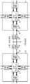
도 2는 도 1의 배열에서 사용하기 위한 SERDES 기능을 사용한 광학-기반 상호연결 장치의 예시적인 종래의 구현을 도시한다.
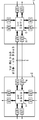
도 3은 예시적인 데이터 통신 장치의 블록도이며, 도 1에 도시된 SERDES 기능은 직접적인 광학적 상호연결 장치로 대체된다.
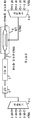
도 4는 도 3의 장치에서 사용될 수 있는 예시적인 직접적인 광학적 상호연결 장치를 도시하며, 여기서 PAM 구조가 다수의 데이터 비트를 동시에 전송하기 위해 사용된다.
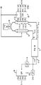
도 5는 본 발명의 광학적 상호연결 장치의 예시적인 실시예를 포함하며, 병렬의 전기적 데이터를 PAM 광학적 신호로 인코딩하는 제 1 MZI 및 클럭 신호를 전송하는 제 2 MZI를 이용하여, 수신단에서 CDR에 대한 필요를 제거한다.
도 6은 본 발명의 광학적 상호연결 장치의 대안적인 실시예를 도시하며, PAM 데이터 신호 및 광학적 클럭 둘 모두를 전송하기 위해 동일한 파장을 사용하고, 두 신호를 전송하기 위해 분리된 광섬유를 제공한다.
도 7은 도 5 또는 도 6의 장치에서 사용될 수 있는 대안적인 광학적 클럭 구조를 도시하며, 상기 대안적인 구조는 주파수가 동기화된 광 신호를 컴퓨팅 칩의 다양한 영역에 분배하기 위한 광학적 분할 장치뿐만 아니라, 제 2 (여분의) 클럭원을 포함한다.
Claims (10)
- 고속 데이터 신호를 전송하기 위한 광학적 상호연결 장치에 있어서, 상기 광학적 상호연결 장치는:
전기적 고속 데이터 신호를 광학적 데이터 신호로 변환하기 위해 제 1 프로세싱 노드와 연결된 전송 컴포넌트;
상기 전송 컴포넌트의 출력에 결합된 광학적 전송 채널; 및
상기 광학적 데이터 신호를 수신하고 상기 수신된 광학적 데이터 신호를 원래의 전기적 고속 데이터 신호로 재변환하기 위해, 제 2 프로세싱 노드와 연결되고 상기 광학적 전송 채널의 출력에 결합되는 수신 컴포넌트를 포함하고,
상기 전송 컴포넌트는:
출력으로 복수의 병렬 위상-정렬된 데이터 신호를 생성하도록, 복수의 N 병렬 데이터 신호 및 전기적 클럭 신호에 응답하는 위상 정렬 엘리먼트;
복수의 N 병렬 위상-정렬된 데이터 신호를 나타내는 PAM(pulse amplitude modulated) 광학적 데이터 신호를 생성하도록, 상기 복수의 N 병렬 위상-정렬된 데이터 신호 및 CW(continuous wave) 광신호에 응답하는 제 1 광학적 변조기; 및
광학적 클럭 출력 신호를 생성하도록, 상기 전기적 클럭 신호 및 CW 광신호에 응답하는 제 2 광학적 변조기를 포함하고,
상기 수신 컴포넌트는:
수신된 PAM 광학적 데이터 신호의 전기적 버전을 생성하도록, 상기 수신된 PAM 광학적 데이터 신호에 응답하는 제 1 O/E(optical/electrical) 변환 장치;
수신된 광학적 클럭 신호의 전기적 버전을 생성하도록, 상기 수신된 광학적 클럭 신호에 응답하는 제 2 O/E 변환 장치; 및
상기 제 1 및 제 2 O/E 변환 장치의 출력으로부터 원래의 복수의 N 병렬 데이터 신호를 복원하도록, 상기 제 1 및 제 2 O/E 변환 장치의 출력에 응답하는 A/D 컨버터를 포함하는 것을 특징으로 하는 광학적 상호연결 장치. - 제 1항에 있어서,
상기 전송 컴포넌트의 제 1 및 제 2 광학적 변조기는 각각 제 1 및 제 2 MZI(Mach-Zehnder interferometer)를 포함하는 것을 특징으로 하는 광학적 상호연결 장치. - 제 2항에 있어서,
상기 제 1 MZI는 멀티-세그먼트 간섭계를 포함하는 것을 특징으로 하는 광학적 상호연결 장치. - 제 3항에 있어서,
상기 제 1 MZI는 복수의 N 병렬 데이터 신호로부터 PAM-N2 출력 신호를 생성하는 것을 특징으로 하는 광학적 상호연결 장치. - 제 1항에 있어서,
상기 전송 컴포넌트는:
제 1 파장(λ1)에서 동작하고, 상기 제 1 광학적 변조기의 입력에 결합된 제 1 광 신호원;
제 2 파장(λ2)에서 동작하고, 상기 제 2 광학적 변조기의 입력에 결합된 제 2 광 신호원; 및
상기 제 1 및 제 2 광학적 변조기로부터의 광학적 출력 신호를 단일 광학적 출력 신호 경로로 결합시키는 광학적 멀티플렉서를 더 포함하고,
상기 수신 컴포넌트는:
파장(λ2)으로 진행하는 광학적 클럭 신호로부터 파장(λ1)으로 진행하는 PAM 데이터 신호를 분리하고, 각각의 신호를 분리된 광학적 신호 경로로 결합시키는 광학적 디멀티플렉서를 더 포함하는 것을 특징으로 하는 광학적 상호연결 장치. - 제 1항에 있어서,
상기 전송 컴포넌트는:
파장(λ1)으로 동작하는 광원; 및
상기 광원으로부터의 출력의 제 1 부분을 상기 제 1 광학적 변조기의 광학적 입력으로 전달하고, 상기 광원으로부터의 출력의 제 2 부분을 상기 제 2 광학적 변조기의 광학적 입력으로 전달하는 광 스플리터를 더 포함하고,
상기 광학적 전송 채널은 한 쌍의 광섬유를 포함하고, 제 1 섬유는 PAM 광학적 데이터 신호의 진행을 지원하고, 제 2 섬유는 광학적 클럭 신호의 진행을 지원하는 것을 특징으로 하는 광학적 상호연결 장치. - 제 1항에 있어서,
상기 제 2 광학적 변조기는, 상기 제 1 프로세싱 노드를 가로질러 주파수가 동기화된 복수의 광학적 클럭 신호를 분산시키는 광학적 클럭 분산 장치를 더 포함하는 것을 특징으로 하는 광학적 상호연결 장치. - 제 7항에 있어서,
상기 광학적 클럭 분산 장치는 상기 제 2 광학적 변조기의 출력에 결합된 광 스플리터를 포함하고,
상기 광 스플리터는 상기 제 1 프로세싱 노드를 가로질러 상기 주파수가 동기화된 복수의 광학적 클럭 신호를 분산시키는 복수의 분기형 도파관을 포함하는 것을 특징으로 하는 광학적 상호연결 장치. - 제 7항에 있어서,
상기 제 2 광학적 변조기는, 원래의 CW 소스가 고장난 것으로 인식되면 백업 소스로 이용하기 위해 제 2 CW 광학적 입력 신호원을 더 포함하는 것을 특징으로 하는 광학적 상호연결 장치. - 제 1항에 있어서,
상기 제 1 광학적 변조기는 광신호를 제공하는 한 쌍의 CW 광학적 입력 신호원을 더 포함하고,
상기 한 쌍의 CW 광학적 입력 신호원 중 제 2 CW 광학적 입력 신호원은, 상기 한 쌍의 CW 광학적 입력 신호원 중 제 1 CW 광학적 입력 신호원이 고장난 것으로 인식되면 백업 소스로 이용되는 것을 특징으로 하는 광학적 상호연결 장치.
Applications Claiming Priority (4)
| Application Number | Priority Date | Filing Date | Title |
|---|---|---|---|
| US18671809P | 2009-06-12 | 2009-06-12 | |
| US61/186,718 | 2009-06-12 | ||
| US12/796,868 US8364042B2 (en) | 2009-06-12 | 2010-06-09 | Optical interconnection arrangement for high speed, high density communication systems |
| US12/796,868 | 2010-06-09 |
Publications (2)
| Publication Number | Publication Date |
|---|---|
| KR20120052931A true KR20120052931A (ko) | 2012-05-24 |
| KR101539136B1 KR101539136B1 (ko) | 2015-07-23 |
Family
ID=43306549
Family Applications (1)
| Application Number | Title | Priority Date | Filing Date |
|---|---|---|---|
| KR1020127000775A Expired - Fee Related KR101539136B1 (ko) | 2009-06-12 | 2010-06-10 | 고속, 고밀도 통신 시스템을 위한 광학적 상호연결 장치 |
Country Status (8)
| Country | Link |
|---|---|
| US (1) | US8364042B2 (ko) |
| EP (1) | EP2441184B1 (ko) |
| JP (1) | JP5522809B2 (ko) |
| KR (1) | KR101539136B1 (ko) |
| CN (1) | CN102804650B (ko) |
| CA (1) | CA2764598C (ko) |
| SG (1) | SG176637A1 (ko) |
| WO (1) | WO2010144658A2 (ko) |
Families Citing this family (22)
| Publication number | Priority date | Publication date | Assignee | Title |
|---|---|---|---|---|
| US8831435B2 (en) * | 2008-03-28 | 2014-09-09 | Centurylink Intellectual Property Llc | System and method for dual wavelength communications of a clock signal |
| US8364042B2 (en) * | 2009-06-12 | 2013-01-29 | Kalpendu Shastri | Optical interconnection arrangement for high speed, high density communication systems |
| US8929689B2 (en) | 2011-03-08 | 2015-01-06 | Cisco Technology, Inc. | Optical modulator utilizing unary encoding and auxiliary modulator section for load balancing |
| JP2013038646A (ja) * | 2011-08-09 | 2013-02-21 | Sony Corp | 信号伝送装置、受信回路、及び、電子機器 |
| WO2013177012A1 (en) * | 2012-05-25 | 2013-11-28 | Corning Incorporated | Systems for differential optical signaling |
| US8983291B1 (en) * | 2012-07-30 | 2015-03-17 | Inphi Corporation | Optical PAM modulation with dual drive mach zehnder modulators and low complexity electrical signaling |
| US9455790B2 (en) | 2012-11-27 | 2016-09-27 | Oe Solutions America, Inc. | High-speed optical receiver implemented using low-speed light receiving element and method for implementing the same |
| US20140281071A1 (en) * | 2013-03-15 | 2014-09-18 | Jianping Jane Xu | Optical memory extension architecture |
| US20150155963A1 (en) * | 2013-12-04 | 2015-06-04 | Cisco Technology, Inc. | Upscaling 20G Optical Transceiver Module |
| JP6126521B2 (ja) * | 2013-12-09 | 2017-05-10 | 日本電信電話株式会社 | 多値光強度変調器 |
| JP6427992B2 (ja) * | 2014-06-30 | 2018-11-28 | 富士通株式会社 | 光伝送システム、送信機、受信機、及び、光伝送方法 |
| FR3034593A1 (ko) * | 2015-04-02 | 2016-10-07 | Commissariat Energie Atomique | |
| US10120210B2 (en) * | 2016-06-03 | 2018-11-06 | International Business Machines Corporation | Feed-forward optical equalization using an electro-optic modulator with a multi-segment electrode and distributed drivers |
| CN106972890B (zh) * | 2017-03-10 | 2019-06-14 | 电子科技大学 | 一种光控光pam信号再生装置 |
| US10725254B2 (en) | 2017-09-20 | 2020-07-28 | Aayuna Inc. | High density opto-electronic interconnection configuration utilizing passive alignment |
| CN112368956B (zh) * | 2018-07-11 | 2022-07-22 | 华为技术有限公司 | 产生信号的装置、方法和系统 |
| KR102186056B1 (ko) * | 2019-07-30 | 2020-12-03 | 한국과학기술원 | 정현파로 세기 변조된 광학 펄스를 입력신호로 사용하는 광학적 시분할 다중화 방식 광전송 시스템 |
| US11006193B2 (en) * | 2019-10-08 | 2021-05-11 | Nokia Solutions And Networks Oy | Electro-optical apparatus having high-throughput electrical data links |
| WO2022060887A1 (en) * | 2020-09-15 | 2022-03-24 | California Institute Of Technology | Optically enabled rf phased-arrays for data transmission |
| US12078908B2 (en) | 2020-10-12 | 2024-09-03 | California Institute Of Technology | Optically enabled RF phased-arrays for data reception |
| US20240152177A1 (en) * | 2021-03-02 | 2024-05-09 | Telefonaktiebolaget Lm Ericsson (Publ) | Clock signal distribution method |
| GB2633816A (en) * | 2023-09-22 | 2025-03-26 | Bae Systems Plc | LDEW optical data link |
Family Cites Families (26)
| Publication number | Priority date | Publication date | Assignee | Title |
|---|---|---|---|---|
| JPS5463603A (en) * | 1977-10-29 | 1979-05-22 | Fujitsu Ltd | Supervisory control system in luminous source double constitution |
| JPH0199336A (ja) * | 1987-10-12 | 1989-04-18 | Nec Corp | 光送信機 |
| JPH0787073A (ja) * | 1993-09-10 | 1995-03-31 | Oki Electric Ind Co Ltd | 並列信号伝送装置 |
| JPH0996746A (ja) * | 1995-09-29 | 1997-04-08 | Fujitsu Ltd | アクティブ光回路シートまたはアクティブ光回路基板 |
| JPH10178387A (ja) * | 1996-12-18 | 1998-06-30 | Nippon Telegr & Teleph Corp <Ntt> | 光インターコネクション装置 |
| JP2001036597A (ja) * | 1999-07-22 | 2001-02-09 | Nec Corp | 並列伝送用光送信装置、及び並列伝送用光送受信システム |
| US6879640B1 (en) * | 1999-10-20 | 2005-04-12 | Broadcom Corporation | Method, apparatus and system for high-speed transmission on fiber optic channel |
| WO2001054317A2 (en) * | 2000-01-17 | 2001-07-26 | Broadcom Corporation | Trellis-coding and pre-equalisation for optical channels |
| US7224906B2 (en) * | 2000-09-26 | 2007-05-29 | Celight, Inc. | Method and system for mitigating nonlinear transmission impairments in fiber-optic communications systems |
| WO2002082694A1 (en) * | 2001-04-04 | 2002-10-17 | Quellan, Inc. | Method and system for decoding multilevel signals |
| US7230979B2 (en) * | 2001-08-17 | 2007-06-12 | Synopsys, Inc. | System and method for high speed digital signaling |
| US7343535B2 (en) * | 2002-02-06 | 2008-03-11 | Avago Technologies General Ip Dte Ltd | Embedded testing capability for integrated serializer/deserializers |
| JP3788945B2 (ja) * | 2002-02-28 | 2006-06-21 | 株式会社東芝 | 多重化光伝送装置 |
| US20030180055A1 (en) * | 2002-03-22 | 2003-09-25 | Kameran Azadet | Optically calibrated pulse amplitude modulated transmission scheme for optical channels |
| EP1531355A4 (en) * | 2002-06-11 | 2008-08-13 | Furukawa Electric Co Ltd | SYSTEM AND METHOD FOR THE OPTICAL WAVELENGTH MULTIPLEX REGENERATION |
| US7099400B2 (en) * | 2003-01-22 | 2006-08-29 | Agere Systems Inc. | Multi-level pulse amplitude modulation receiver |
| JP4118245B2 (ja) * | 2004-03-30 | 2008-07-16 | 株式会社東芝 | 画像送信装置、画像受信装置および画像伝送システム |
| US7570708B2 (en) * | 2005-01-31 | 2009-08-04 | Agere Systems Inc. | Serdes auto calibration and load balancing |
| JPWO2007013356A1 (ja) * | 2005-07-26 | 2009-02-05 | 株式会社アドバンテスト | 信号送信装置、信号受信装置、試験装置、テストモジュール、及び半導体チップ |
| US7558487B2 (en) * | 2005-09-25 | 2009-07-07 | Alcatel-Lucent Usa Inc. | Multilevel amplitude and phase encoded signal generation |
| JP4781094B2 (ja) | 2005-11-30 | 2011-09-28 | 富士通株式会社 | 光送信装置 |
| US7483597B2 (en) * | 2006-10-19 | 2009-01-27 | Lightwire, Inc. | Optical modulator utilizing multi-level signaling |
| JP4458169B2 (ja) * | 2008-02-04 | 2010-04-28 | 沖電気工業株式会社 | 光変調器及び光信号発生装置 |
| US8238014B2 (en) * | 2008-09-08 | 2012-08-07 | Luxtera Inc. | Method and circuit for encoding multi-level pulse amplitude modulated signals using integrated optoelectronic devices |
| US8364042B2 (en) * | 2009-06-12 | 2013-01-29 | Kalpendu Shastri | Optical interconnection arrangement for high speed, high density communication systems |
| US8340529B2 (en) * | 2009-06-13 | 2012-12-25 | Kalpendu Shastri | HDMI TMDS optical signal transmission using PAM technique |
-
2010
- 2010-06-09 US US12/796,868 patent/US8364042B2/en active Active
- 2010-06-10 WO PCT/US2010/038103 patent/WO2010144658A2/en not_active Ceased
- 2010-06-10 JP JP2012515126A patent/JP5522809B2/ja active Active
- 2010-06-10 SG SG2011089307A patent/SG176637A1/en unknown
- 2010-06-10 EP EP10786828.3A patent/EP2441184B1/en active Active
- 2010-06-10 CN CN201080025226.7A patent/CN102804650B/zh active Active
- 2010-06-10 KR KR1020127000775A patent/KR101539136B1/ko not_active Expired - Fee Related
- 2010-06-10 CA CA2764598A patent/CA2764598C/en not_active Expired - Fee Related
Also Published As
| Publication number | Publication date |
|---|---|
| WO2010144658A3 (en) | 2011-02-24 |
| CN102804650A (zh) | 2012-11-28 |
| KR101539136B1 (ko) | 2015-07-23 |
| WO2010144658A2 (en) | 2010-12-16 |
| CA2764598C (en) | 2015-10-27 |
| EP2441184B1 (en) | 2018-11-21 |
| EP2441184A4 (en) | 2017-08-02 |
| US20100316391A1 (en) | 2010-12-16 |
| CA2764598A1 (en) | 2010-12-16 |
| EP2441184A2 (en) | 2012-04-18 |
| JP2012529874A (ja) | 2012-11-22 |
| JP5522809B2 (ja) | 2014-06-18 |
| CN102804650B (zh) | 2015-07-08 |
| SG176637A1 (en) | 2012-01-30 |
| US8364042B2 (en) | 2013-01-29 |
Similar Documents
| Publication | Publication Date | Title |
|---|---|---|
| KR101539136B1 (ko) | 고속, 고밀도 통신 시스템을 위한 광학적 상호연결 장치 | |
| US11705972B2 (en) | Pooled memory system enabled by monolithic in-package optical I/O | |
| US7738486B2 (en) | Multi-mode integrated circuit for use in optoelectronic devices | |
| US10120826B2 (en) | Single-chip control module for an integrated system-on-a-chip for silicon photonics | |
| US9774391B2 (en) | Built-in self test for loopback on communication system on chip | |
| CN113132009A (zh) | 一种相干光模块及光通信系统 | |
| JP2023528256A (ja) | 光周波数コム発生器を用いた集積cmos光/電子wdm通信システム | |
| US10409758B1 (en) | Single-chip control module for an integrated system-on-a-chip for silicon photonics | |
| US20240077781A1 (en) | Computer architecture with disaggregated memory and high-bandwidth communication interconnects | |
| CN219676335U (zh) | 多通道有源光缆光子集成芯片及有源光缆 | |
| US8639114B2 (en) | DPSK modulation-demodulation method, and optical communication device and optical communication system using the same | |
| EP2137847B1 (en) | Multi-mode integrated circuit for use in optoelectronic devices | |
| US20060126993A1 (en) | SOI-based optical interconnect arrangement | |
| Bhargava et al. | A UCIe Optical I/O Retimer Chiplet for AI Scale-up Fabrics | |
| US7197249B2 (en) | Method and system for synchronizing optical clocks | |
| US20250323747A1 (en) | Multi-Chip Optical Data Communication Systems Implementing Common Remote Optical Power Supply | |
| Ho et al. | Optical interconnect for high-end computer systems | |
| US20220173825A1 (en) | Optical network on chip for processor communication | |
| WO2024261482A1 (en) | A system and method for routing an optical signal | |
| JP2005204234A (ja) | Cpu光接続システム |
Legal Events
| Date | Code | Title | Description |
|---|---|---|---|
| PA0105 | International application |
St.27 status event code: A-0-1-A10-A15-nap-PA0105 |
|
| PG1501 | Laying open of application |
St.27 status event code: A-1-1-Q10-Q12-nap-PG1501 |
|
| PN2301 | Change of applicant |
St.27 status event code: A-3-3-R10-R13-asn-PN2301 St.27 status event code: A-3-3-R10-R11-asn-PN2301 |
|
| N231 | Notification of change of applicant | ||
| PN2301 | Change of applicant |
St.27 status event code: A-3-3-R10-R13-asn-PN2301 St.27 status event code: A-3-3-R10-R11-asn-PN2301 |
|
| N231 | Notification of change of applicant | ||
| PN2301 | Change of applicant |
St.27 status event code: A-3-3-R10-R13-asn-PN2301 St.27 status event code: A-3-3-R10-R11-asn-PN2301 |
|
| A201 | Request for examination | ||
| A302 | Request for accelerated examination | ||
| E13-X000 | Pre-grant limitation requested |
St.27 status event code: A-2-3-E10-E13-lim-X000 |
|
| P11-X000 | Amendment of application requested |
St.27 status event code: A-2-2-P10-P11-nap-X000 |
|
| P13-X000 | Application amended |
St.27 status event code: A-2-2-P10-P13-nap-X000 |
|
| PA0201 | Request for examination |
St.27 status event code: A-1-2-D10-D11-exm-PA0201 |
|
| PA0302 | Request for accelerated examination |
St.27 status event code: A-1-2-D10-D17-exm-PA0302 St.27 status event code: A-1-2-D10-D16-exm-PA0302 |
|
| E701 | Decision to grant or registration of patent right | ||
| PE0701 | Decision of registration |
St.27 status event code: A-1-2-D10-D22-exm-PE0701 |
|
| GRNT | Written decision to grant | ||
| PR0701 | Registration of establishment |
St.27 status event code: A-2-4-F10-F11-exm-PR0701 |
|
| PR1002 | Payment of registration fee |
St.27 status event code: A-2-2-U10-U12-oth-PR1002 Fee payment year number: 1 |
|
| PG1601 | Publication of registration |
St.27 status event code: A-4-4-Q10-Q13-nap-PG1601 |
|
| FPAY | Annual fee payment |
Payment date: 20180710 Year of fee payment: 4 |
|
| PR1001 | Payment of annual fee |
St.27 status event code: A-4-4-U10-U11-oth-PR1001 Fee payment year number: 4 |
|
| FPAY | Annual fee payment |
Payment date: 20190709 Year of fee payment: 5 |
|
| PR1001 | Payment of annual fee |
St.27 status event code: A-4-4-U10-U11-oth-PR1001 Fee payment year number: 5 |
|
| PC1903 | Unpaid annual fee |
St.27 status event code: A-4-4-U10-U13-oth-PC1903 Not in force date: 20200718 Payment event data comment text: Termination Category : DEFAULT_OF_REGISTRATION_FEE |
|
| PC1903 | Unpaid annual fee |
St.27 status event code: N-4-6-H10-H13-oth-PC1903 Ip right cessation event data comment text: Termination Category : DEFAULT_OF_REGISTRATION_FEE Not in force date: 20200718 |