KR20120001621A - Manufacturing method of semiconductor packages - Google Patents
Manufacturing method of semiconductor packages Download PDFInfo
- Publication number
- KR20120001621A KR20120001621A KR1020110060989A KR20110060989A KR20120001621A KR 20120001621 A KR20120001621 A KR 20120001621A KR 1020110060989 A KR1020110060989 A KR 1020110060989A KR 20110060989 A KR20110060989 A KR 20110060989A KR 20120001621 A KR20120001621 A KR 20120001621A
- Authority
- KR
- South Korea
- Prior art keywords
- substrate
- substrate material
- solder
- ball
- bonding pad
- Prior art date
Links
Images


Classifications
-
- H—ELECTRICITY
- H01—ELECTRIC ELEMENTS
- H01L—SEMICONDUCTOR DEVICES NOT COVERED BY CLASS H10
- H01L23/00—Details of semiconductor or other solid state devices
- H01L23/48—Arrangements for conducting electric current to or from the solid state body in operation, e.g. leads, terminal arrangements ; Selection of materials therefor
-
- H—ELECTRICITY
- H01—ELECTRIC ELEMENTS
- H01L—SEMICONDUCTOR DEVICES NOT COVERED BY CLASS H10
- H01L21/00—Processes or apparatus adapted for the manufacture or treatment of semiconductor or solid state devices or of parts thereof
- H01L21/02—Manufacture or treatment of semiconductor devices or of parts thereof
- H01L21/04—Manufacture or treatment of semiconductor devices or of parts thereof the devices having at least one potential-jump barrier or surface barrier, e.g. PN junction, depletion layer or carrier concentration layer
- H01L21/50—Assembly of semiconductor devices using processes or apparatus not provided for in a single one of the subgroups H01L21/06 - H01L21/326, e.g. sealing of a cap to a base of a container
- H01L21/56—Encapsulations, e.g. encapsulation layers, coatings
- H01L21/565—Moulds
-
- H—ELECTRICITY
- H01—ELECTRIC ELEMENTS
- H01L—SEMICONDUCTOR DEVICES NOT COVERED BY CLASS H10
- H01L21/00—Processes or apparatus adapted for the manufacture or treatment of semiconductor or solid state devices or of parts thereof
- H01L21/02—Manufacture or treatment of semiconductor devices or of parts thereof
- H01L21/04—Manufacture or treatment of semiconductor devices or of parts thereof the devices having at least one potential-jump barrier or surface barrier, e.g. PN junction, depletion layer or carrier concentration layer
- H01L21/50—Assembly of semiconductor devices using processes or apparatus not provided for in a single one of the subgroups H01L21/06 - H01L21/326, e.g. sealing of a cap to a base of a container
- H01L21/56—Encapsulations, e.g. encapsulation layers, coatings
- H01L21/561—Batch processing
-
- H—ELECTRICITY
- H01—ELECTRIC ELEMENTS
- H01L—SEMICONDUCTOR DEVICES NOT COVERED BY CLASS H10
- H01L21/00—Processes or apparatus adapted for the manufacture or treatment of semiconductor or solid state devices or of parts thereof
- H01L21/70—Manufacture or treatment of devices consisting of a plurality of solid state components formed in or on a common substrate or of parts thereof; Manufacture of integrated circuit devices or of parts thereof
- H01L21/77—Manufacture or treatment of devices consisting of a plurality of solid state components or integrated circuits formed in, or on, a common substrate
- H01L21/78—Manufacture or treatment of devices consisting of a plurality of solid state components or integrated circuits formed in, or on, a common substrate with subsequent division of the substrate into plural individual devices
-
- H—ELECTRICITY
- H01—ELECTRIC ELEMENTS
- H01L—SEMICONDUCTOR DEVICES NOT COVERED BY CLASS H10
- H01L23/00—Details of semiconductor or other solid state devices
- H01L23/28—Encapsulations, e.g. encapsulating layers, coatings, e.g. for protection
-
- H—ELECTRICITY
- H01—ELECTRIC ELEMENTS
- H01L—SEMICONDUCTOR DEVICES NOT COVERED BY CLASS H10
- H01L23/00—Details of semiconductor or other solid state devices
- H01L23/28—Encapsulations, e.g. encapsulating layers, coatings, e.g. for protection
- H01L23/31—Encapsulations, e.g. encapsulating layers, coatings, e.g. for protection characterised by the arrangement or shape
- H01L23/3107—Encapsulations, e.g. encapsulating layers, coatings, e.g. for protection characterised by the arrangement or shape the device being completely enclosed
- H01L23/3121—Encapsulations, e.g. encapsulating layers, coatings, e.g. for protection characterised by the arrangement or shape the device being completely enclosed a substrate forming part of the encapsulation
- H01L23/3128—Encapsulations, e.g. encapsulating layers, coatings, e.g. for protection characterised by the arrangement or shape the device being completely enclosed a substrate forming part of the encapsulation the substrate having spherical bumps for external connection
-
- H—ELECTRICITY
- H01—ELECTRIC ELEMENTS
- H01L—SEMICONDUCTOR DEVICES NOT COVERED BY CLASS H10
- H01L23/00—Details of semiconductor or other solid state devices
- H01L23/48—Arrangements for conducting electric current to or from the solid state body in operation, e.g. leads, terminal arrangements ; Selection of materials therefor
- H01L23/481—Internal lead connections, e.g. via connections, feedthrough structures
-
- H—ELECTRICITY
- H01—ELECTRIC ELEMENTS
- H01L—SEMICONDUCTOR DEVICES NOT COVERED BY CLASS H10
- H01L23/00—Details of semiconductor or other solid state devices
- H01L23/48—Arrangements for conducting electric current to or from the solid state body in operation, e.g. leads, terminal arrangements ; Selection of materials therefor
- H01L23/488—Arrangements for conducting electric current to or from the solid state body in operation, e.g. leads, terminal arrangements ; Selection of materials therefor consisting of soldered or bonded constructions
- H01L23/498—Leads, i.e. metallisations or lead-frames on insulating substrates, e.g. chip carriers
- H01L23/49833—Leads, i.e. metallisations or lead-frames on insulating substrates, e.g. chip carriers the chip support structure consisting of a plurality of insulating substrates
-
- H—ELECTRICITY
- H01—ELECTRIC ELEMENTS
- H01L—SEMICONDUCTOR DEVICES NOT COVERED BY CLASS H10
- H01L24/00—Arrangements for connecting or disconnecting semiconductor or solid-state bodies; Methods or apparatus related thereto
- H01L24/93—Batch processes
- H01L24/95—Batch processes at chip-level, i.e. with connecting carried out on a plurality of singulated devices, i.e. on diced chips
- H01L24/97—Batch processes at chip-level, i.e. with connecting carried out on a plurality of singulated devices, i.e. on diced chips the devices being connected to a common substrate, e.g. interposer, said common substrate being separable into individual assemblies after connecting
-
- H—ELECTRICITY
- H01—ELECTRIC ELEMENTS
- H01L—SEMICONDUCTOR DEVICES NOT COVERED BY CLASS H10
- H01L2224/00—Indexing scheme for arrangements for connecting or disconnecting semiconductor or solid-state bodies and methods related thereto as covered by H01L24/00
- H01L2224/01—Means for bonding being attached to, or being formed on, the surface to be connected, e.g. chip-to-package, die-attach, "first-level" interconnects; Manufacturing methods related thereto
- H01L2224/10—Bump connectors; Manufacturing methods related thereto
- H01L2224/15—Structure, shape, material or disposition of the bump connectors after the connecting process
- H01L2224/16—Structure, shape, material or disposition of the bump connectors after the connecting process of an individual bump connector
- H01L2224/161—Disposition
- H01L2224/16151—Disposition the bump connector connecting between a semiconductor or solid-state body and an item not being a semiconductor or solid-state body, e.g. chip-to-substrate, chip-to-passive
- H01L2224/16221—Disposition the bump connector connecting between a semiconductor or solid-state body and an item not being a semiconductor or solid-state body, e.g. chip-to-substrate, chip-to-passive the body and the item being stacked
- H01L2224/16225—Disposition the bump connector connecting between a semiconductor or solid-state body and an item not being a semiconductor or solid-state body, e.g. chip-to-substrate, chip-to-passive the body and the item being stacked the item being non-metallic, e.g. insulating substrate with or without metallisation
- H01L2224/16227—Disposition the bump connector connecting between a semiconductor or solid-state body and an item not being a semiconductor or solid-state body, e.g. chip-to-substrate, chip-to-passive the body and the item being stacked the item being non-metallic, e.g. insulating substrate with or without metallisation the bump connector connecting to a bond pad of the item
-
- H—ELECTRICITY
- H01—ELECTRIC ELEMENTS
- H01L—SEMICONDUCTOR DEVICES NOT COVERED BY CLASS H10
- H01L2224/00—Indexing scheme for arrangements for connecting or disconnecting semiconductor or solid-state bodies and methods related thereto as covered by H01L24/00
- H01L2224/01—Means for bonding being attached to, or being formed on, the surface to be connected, e.g. chip-to-package, die-attach, "first-level" interconnects; Manufacturing methods related thereto
- H01L2224/26—Layer connectors, e.g. plate connectors, solder or adhesive layers; Manufacturing methods related thereto
- H01L2224/31—Structure, shape, material or disposition of the layer connectors after the connecting process
- H01L2224/32—Structure, shape, material or disposition of the layer connectors after the connecting process of an individual layer connector
- H01L2224/321—Disposition
- H01L2224/32151—Disposition the layer connector connecting between a semiconductor or solid-state body and an item not being a semiconductor or solid-state body, e.g. chip-to-substrate, chip-to-passive
- H01L2224/32221—Disposition the layer connector connecting between a semiconductor or solid-state body and an item not being a semiconductor or solid-state body, e.g. chip-to-substrate, chip-to-passive the body and the item being stacked
- H01L2224/32225—Disposition the layer connector connecting between a semiconductor or solid-state body and an item not being a semiconductor or solid-state body, e.g. chip-to-substrate, chip-to-passive the body and the item being stacked the item being non-metallic, e.g. insulating substrate with or without metallisation
-
- H—ELECTRICITY
- H01—ELECTRIC ELEMENTS
- H01L—SEMICONDUCTOR DEVICES NOT COVERED BY CLASS H10
- H01L2224/00—Indexing scheme for arrangements for connecting or disconnecting semiconductor or solid-state bodies and methods related thereto as covered by H01L24/00
- H01L2224/73—Means for bonding being of different types provided for in two or more of groups H01L2224/10, H01L2224/18, H01L2224/26, H01L2224/34, H01L2224/42, H01L2224/50, H01L2224/63, H01L2224/71
- H01L2224/732—Location after the connecting process
- H01L2224/73201—Location after the connecting process on the same surface
- H01L2224/73203—Bump and layer connectors
- H01L2224/73204—Bump and layer connectors the bump connector being embedded into the layer connector
-
- H—ELECTRICITY
- H01—ELECTRIC ELEMENTS
- H01L—SEMICONDUCTOR DEVICES NOT COVERED BY CLASS H10
- H01L2224/00—Indexing scheme for arrangements for connecting or disconnecting semiconductor or solid-state bodies and methods related thereto as covered by H01L24/00
- H01L2224/93—Batch processes
- H01L2224/95—Batch processes at chip-level, i.e. with connecting carried out on a plurality of singulated devices, i.e. on diced chips
- H01L2224/97—Batch processes at chip-level, i.e. with connecting carried out on a plurality of singulated devices, i.e. on diced chips the devices being connected to a common substrate, e.g. interposer, said common substrate being separable into individual assemblies after connecting
-
- H—ELECTRICITY
- H01—ELECTRIC ELEMENTS
- H01L—SEMICONDUCTOR DEVICES NOT COVERED BY CLASS H10
- H01L23/00—Details of semiconductor or other solid state devices
- H01L23/48—Arrangements for conducting electric current to or from the solid state body in operation, e.g. leads, terminal arrangements ; Selection of materials therefor
- H01L23/488—Arrangements for conducting electric current to or from the solid state body in operation, e.g. leads, terminal arrangements ; Selection of materials therefor consisting of soldered or bonded constructions
- H01L23/498—Leads, i.e. metallisations or lead-frames on insulating substrates, e.g. chip carriers
- H01L23/49811—Additional leads joined to the metallisation on the insulating substrate, e.g. pins, bumps, wires, flat leads
- H01L23/49816—Spherical bumps on the substrate for external connection, e.g. ball grid arrays [BGA]
-
- H—ELECTRICITY
- H01—ELECTRIC ELEMENTS
- H01L—SEMICONDUCTOR DEVICES NOT COVERED BY CLASS H10
- H01L23/00—Details of semiconductor or other solid state devices
- H01L23/48—Arrangements for conducting electric current to or from the solid state body in operation, e.g. leads, terminal arrangements ; Selection of materials therefor
- H01L23/488—Arrangements for conducting electric current to or from the solid state body in operation, e.g. leads, terminal arrangements ; Selection of materials therefor consisting of soldered or bonded constructions
- H01L23/498—Leads, i.e. metallisations or lead-frames on insulating substrates, e.g. chip carriers
- H01L23/49822—Multilayer substrates
-
- H—ELECTRICITY
- H01—ELECTRIC ELEMENTS
- H01L—SEMICONDUCTOR DEVICES NOT COVERED BY CLASS H10
- H01L24/00—Arrangements for connecting or disconnecting semiconductor or solid-state bodies; Methods or apparatus related thereto
- H01L24/01—Means for bonding being attached to, or being formed on, the surface to be connected, e.g. chip-to-package, die-attach, "first-level" interconnects; Manufacturing methods related thereto
- H01L24/10—Bump connectors ; Manufacturing methods related thereto
- H01L24/15—Structure, shape, material or disposition of the bump connectors after the connecting process
- H01L24/16—Structure, shape, material or disposition of the bump connectors after the connecting process of an individual bump connector
-
- H—ELECTRICITY
- H01—ELECTRIC ELEMENTS
- H01L—SEMICONDUCTOR DEVICES NOT COVERED BY CLASS H10
- H01L24/00—Arrangements for connecting or disconnecting semiconductor or solid-state bodies; Methods or apparatus related thereto
- H01L24/73—Means for bonding being of different types provided for in two or more of groups H01L24/10, H01L24/18, H01L24/26, H01L24/34, H01L24/42, H01L24/50, H01L24/63, H01L24/71
-
- H—ELECTRICITY
- H01—ELECTRIC ELEMENTS
- H01L—SEMICONDUCTOR DEVICES NOT COVERED BY CLASS H10
- H01L2924/00—Indexing scheme for arrangements or methods for connecting or disconnecting semiconductor or solid-state bodies as covered by H01L24/00
- H01L2924/0001—Technical content checked by a classifier
- H01L2924/00014—Technical content checked by a classifier the subject-matter covered by the group, the symbol of which is combined with the symbol of this group, being disclosed without further technical details
-
- H—ELECTRICITY
- H01—ELECTRIC ELEMENTS
- H01L—SEMICONDUCTOR DEVICES NOT COVERED BY CLASS H10
- H01L2924/00—Indexing scheme for arrangements or methods for connecting or disconnecting semiconductor or solid-state bodies as covered by H01L24/00
- H01L2924/01—Chemical elements
- H01L2924/01005—Boron [B]
-
- H—ELECTRICITY
- H01—ELECTRIC ELEMENTS
- H01L—SEMICONDUCTOR DEVICES NOT COVERED BY CLASS H10
- H01L2924/00—Indexing scheme for arrangements or methods for connecting or disconnecting semiconductor or solid-state bodies as covered by H01L24/00
- H01L2924/01—Chemical elements
- H01L2924/01006—Carbon [C]
-
- H—ELECTRICITY
- H01—ELECTRIC ELEMENTS
- H01L—SEMICONDUCTOR DEVICES NOT COVERED BY CLASS H10
- H01L2924/00—Indexing scheme for arrangements or methods for connecting or disconnecting semiconductor or solid-state bodies as covered by H01L24/00
- H01L2924/01—Chemical elements
- H01L2924/01029—Copper [Cu]
-
- H—ELECTRICITY
- H01—ELECTRIC ELEMENTS
- H01L—SEMICONDUCTOR DEVICES NOT COVERED BY CLASS H10
- H01L2924/00—Indexing scheme for arrangements or methods for connecting or disconnecting semiconductor or solid-state bodies as covered by H01L24/00
- H01L2924/01—Chemical elements
- H01L2924/01033—Arsenic [As]
-
- H—ELECTRICITY
- H01—ELECTRIC ELEMENTS
- H01L—SEMICONDUCTOR DEVICES NOT COVERED BY CLASS H10
- H01L2924/00—Indexing scheme for arrangements or methods for connecting or disconnecting semiconductor or solid-state bodies as covered by H01L24/00
- H01L2924/01—Chemical elements
- H01L2924/01047—Silver [Ag]
-
- H—ELECTRICITY
- H01—ELECTRIC ELEMENTS
- H01L—SEMICONDUCTOR DEVICES NOT COVERED BY CLASS H10
- H01L2924/00—Indexing scheme for arrangements or methods for connecting or disconnecting semiconductor or solid-state bodies as covered by H01L24/00
- H01L2924/01—Chemical elements
- H01L2924/01079—Gold [Au]
-
- H—ELECTRICITY
- H01—ELECTRIC ELEMENTS
- H01L—SEMICONDUCTOR DEVICES NOT COVERED BY CLASS H10
- H01L2924/00—Indexing scheme for arrangements or methods for connecting or disconnecting semiconductor or solid-state bodies as covered by H01L24/00
- H01L2924/013—Alloys
- H01L2924/014—Solder alloys
-
- H—ELECTRICITY
- H01—ELECTRIC ELEMENTS
- H01L—SEMICONDUCTOR DEVICES NOT COVERED BY CLASS H10
- H01L2924/00—Indexing scheme for arrangements or methods for connecting or disconnecting semiconductor or solid-state bodies as covered by H01L24/00
- H01L2924/15—Details of package parts other than the semiconductor or other solid state devices to be connected
- H01L2924/151—Die mounting substrate
- H01L2924/1517—Multilayer substrate
- H01L2924/15192—Resurf arrangement of the internal vias
-
- H—ELECTRICITY
- H01—ELECTRIC ELEMENTS
- H01L—SEMICONDUCTOR DEVICES NOT COVERED BY CLASS H10
- H01L2924/00—Indexing scheme for arrangements or methods for connecting or disconnecting semiconductor or solid-state bodies as covered by H01L24/00
- H01L2924/15—Details of package parts other than the semiconductor or other solid state devices to be connected
- H01L2924/151—Die mounting substrate
- H01L2924/153—Connection portion
- H01L2924/1531—Connection portion the connection portion being formed only on the surface of the substrate opposite to the die mounting surface
- H01L2924/15311—Connection portion the connection portion being formed only on the surface of the substrate opposite to the die mounting surface being a ball array, e.g. BGA
-
- H—ELECTRICITY
- H01—ELECTRIC ELEMENTS
- H01L—SEMICONDUCTOR DEVICES NOT COVERED BY CLASS H10
- H01L2924/00—Indexing scheme for arrangements or methods for connecting or disconnecting semiconductor or solid-state bodies as covered by H01L24/00
- H01L2924/15—Details of package parts other than the semiconductor or other solid state devices to be connected
- H01L2924/151—Die mounting substrate
- H01L2924/153—Connection portion
- H01L2924/1532—Connection portion the connection portion being formed on the die mounting surface of the substrate
- H01L2924/1533—Connection portion the connection portion being formed on the die mounting surface of the substrate the connection portion being formed both on the die mounting surface of the substrate and outside the die mounting surface of the substrate
- H01L2924/15331—Connection portion the connection portion being formed on the die mounting surface of the substrate the connection portion being formed both on the die mounting surface of the substrate and outside the die mounting surface of the substrate being a ball array, e.g. BGA
-
- H—ELECTRICITY
- H01—ELECTRIC ELEMENTS
- H01L—SEMICONDUCTOR DEVICES NOT COVERED BY CLASS H10
- H01L2924/00—Indexing scheme for arrangements or methods for connecting or disconnecting semiconductor or solid-state bodies as covered by H01L24/00
- H01L2924/15—Details of package parts other than the semiconductor or other solid state devices to be connected
- H01L2924/181—Encapsulation
Abstract
Description
본 발명은 상하 기판의 사이에 반도체 소자를 배치해서 형성한 반도체 패키지의 제조 방법에 관한 것이다.This invention relates to the manufacturing method of the semiconductor package formed by arrange | positioning a semiconductor element between upper and lower board | substrates.
일본국 특개2008-135781호 공보에는, 상하 기판의 사이에 반도체 소자를 배치하고, 반도체 소자의 주위에 몰드 수지를 충전해서 형성한 반도체 패키지가 제안되어 있다. 상하 기판의 간격을 유지하기 위해서 스페이서 부재를 통해 하측 기판에 상측 기판이 고정되고, 그 사이에 몰드 수지가 충전된다. 스페이서 부재를 통해 상측 기판과 하측 기판을 전기적으로 접속할 수 있다. 외부 접속 단자는 하측 기판의 이면에 설치되어, 상측 기판에는 전자 부품을 탑재할 수 있다.Japanese Patent Laid-Open No. 2008-135781 proposes a semiconductor package in which a semiconductor element is disposed between upper and lower substrates, and a mold resin is filled around the semiconductor element. In order to maintain the space | interval of an upper and lower board | substrate, an upper board | substrate is fixed to a lower board | substrate through a spacer member, and mold resin is filled in between. The upper substrate and the lower substrate can be electrically connected through the spacer member. The external connection terminal is provided on the rear surface of the lower substrate, and electronic components can be mounted on the upper substrate.
이상과 같은 구조의 반도체 패키지에 있어서, 스페이서 부재로서 동 코어(copper-core) 땜납 볼을 이용하는 것이 제안되어 있다. 동 코어 땜납 볼은 동 코어 볼, 및 동 코어 볼의 주위를 덮은 땜납을 포함한다. 땜납은 접합재로서 기능하고, 동 코어 볼은 스페이서로서 기능한다. 즉, 상측 기판의 접속 패드와 하측 기판의 접속 패드 사이에 동 코어 땜납 볼을 끼운 상태에서 땜납을 리플로우함으로써, 상측 기판의 접속 패드와 하측 기판의 접속 패드를 각각 땜납 접합한다. 땜납 내부의 동 코어 볼이 상측 기판과 하측 기판 사이에 끼워진 상태로 설정된다. 이로써, 각각의 구리 코어 볼은 스페이서로서 기능한다. 따라서, 상측 기판과 하측 기판 사이의 거리는, 동 코어 볼의 크기에 의해 결정되어, 일정하게 유지될 수 있다.In the semiconductor package having the above structure, it is proposed to use a copper-core solder ball as the spacer member. The copper core solder ball includes a copper core ball and solder covering the copper core ball. Solder functions as a joining material, and the copper core ball functions as a spacer. That is, by reflowing solder in a state where the copper solder ball is sandwiched between the connection pad of the upper substrate and the connection pad of the lower substrate, the solder pads are connected to the connection pad of the upper substrate and the connection pad of the lower substrate, respectively. The copper core ball inside the solder is set in a state sandwiched between the upper substrate and the lower substrate. As a result, each copper core ball functions as a spacer. Therefore, the distance between the upper substrate and the lower substrate is determined by the size of the core ball, and can be kept constant.
동 코어 땜납 볼을 이용하여 상측 기판과 하측 기판을 접속한 후, 상측 기판과 하측 기판 사이에는 몰드 수지가 충전되어, 상측 기판과 하측 기판이 서로 확실하게 고정된다. 그러므로, 하측 기판에 실장된 반도체 소자와 동 코어 땜납 볼은, 몰드 수지 내에 메워넣어진다.After connecting the upper substrate and the lower substrate using the copper solder ball, a mold resin is filled between the upper substrate and the lower substrate, and the upper substrate and the lower substrate are securely fixed to each other. Therefore, the semiconductor element mounted on the lower substrate and the copper core solder ball are embedded in the mold resin.
상술한 바와 같이, 동 코어 땜납 볼로 상측 기판과 하측 기판을 접속 및 고정할 경우, 몰드 수지 중에 동 코어 볼과 땜납이 가둬진다. 이러한 반도체 패키지를 회로 기판에 실장하기 위해서, 반도체 패키지의 외부 접속 단자로서 기능하는 땜납 볼의 리플로우를 행하면, 리플로우에 의해 가해진 열에 의해 몰드 수지 내부의 동 코어 볼의 주위의 땜납도 용융한다.As described above, when the upper substrate and the lower substrate are connected and fixed by the copper core solder ball, the copper core ball and the solder are confined in the mold resin. In order to mount such a semiconductor package on a circuit board, when the solder ball which functions as an external connection terminal of the semiconductor package is reflowed, the solder around the copper core ball inside the mold resin is also melted by the heat applied by the reflow.
동 코어 볼이 동 코어 볼의 주위에 있어서 땜납이 용융하는 온도까지 가열되면, 동 코어 볼 및 땜납은 열팽창되고, 이로써 그 체적이 커지려고 한다. 그러나, 동 코어 볼과 땜납은 몰드 수지 중에 가둬져 있으므로, 용융한 땜납의 압력이 상승하게 된다. 그리고, 몰드 수지가 상측 기판이나 하측 기판과 접착해 있는 부분에 있어서 접착이 약한 부분이 있으면, 용융한 땜납은 그 접착이 약한 부분에 진입할 수 있다.When the copper core ball is heated to a temperature at which the solder melts around the copper core ball, the copper core ball and the solder are thermally expanded, and the volume thereof is about to increase. However, since the core ball and the solder are confined in the mold resin, the pressure of the molten solder is increased. And if there is a part with weak adhesion in the part which mold resin adhere | attaches with an upper board | substrate or a lower board | substrate, molten solder can enter into the part with weak adhesion.
예를 들면, 몰드 수지와 기판 상의 솔더레지스트 사이, 혹은 솔더레지스트와 배선 패턴 사이에 접착이 약한 부분이 있으면, 용융한 땜납은 몰드 수지나 솔더레지스트를 박리하면서 접착이 약한 부분에 진입해 간다. 땜납이 솔더레지스트나 배선 패턴을 따라 진입하면, 진입한 땜납으로 인해 인접한 접속 패드가 단락하거나, 배선 패턴이 단락할 수 있다.For example, if there is a weak adhesion portion between the mold resin and the solder resist on the substrate, or between the solder resist and the wiring pattern, the molten solder enters the weak adhesion portion while peeling off the mold resin or the solder resist. When the solder enters along the solder resist or the wiring pattern, the adjacent solder may short or the wiring pattern may short due to the solder.
그래서, 동 코어 땜납 볼을 스페이서 부재로서 이용해서 상측 기판과 하측 기판을 접속해도, 몰드 수지 내에서 용융한 땜납이 상술한 바와 같은 문제를 야기하지 않는 기술의 개발이 요망되고 있다.Therefore, even if the upper substrate and the lower substrate are connected by using the copper solder ball as a spacer member, there is a demand for the development of a technique in which the molten solder in the mold resin does not cause the above problems.
본 발명의 1 실시 태양에 따르면, 복수의 반도체 패키지를 일괄해서 제조하는 제조 방법이 제공되고, 각각의 상기 반도체 패키지는 스페이서 부재를 통해 서로 접속된 상측 기판 및 하측 기판과, 상기 상측 기판과 상기 하측 기판 사이에 위치되며, 상기 하측 기판에 실장된 반도체 소자와, 상기 상측 기판과 상기 하측 기판 사이의 공간에 충전된 몰드 수지를 포함하고, 상기 제조 방법은, 상기 상측 기판 및 상기 상측 기판의 주위의 연장부를 포함하는 상측 기판용 기판재를 준비하고, 상기 상측 기판에 형성된 접합 패드에 상기 스페이서 부재로서 도전성 코어 볼을 접합하고 또한 상기 연장부에 형성된 접합 패드에 코어 볼을 접합함과 함께, 상기 하측 기판 및 상기 하측 기판의 주위의 연장부를 포함하는 하측 기판용 기판재를 준비하는 단계와; 상기 상측 기판용 기판재의 연장부에 형성된 접합 패드를 상기 코어 볼을 통해 상기 하측 기판용 기판재의 연장부에 형성된 접합 패드에 접합하고, 또한 상기 상측 기판용 기판재의 상기 상측 기판에 상당하는 영역에 형성된 접합 패드를 상기 코어 볼 및 상기 도전성 코어 볼을 통해 상기 하측 기판용 기판재의 상기 하측 기판에 상당하는 영역에 형성된 접합 패드에 전기적으로 접속함으로써, 상기 상측 기판용 기판재를 상기 하측 기판용 기판재에 접속하는 단계와; 상기 상측 기판용 기판재와 상기 하측 기판용 기판재 사이에 몰드 수지를 충전함으로써, 상기 상측 기판용 기판재를 상기 하측 기판용 기판재에 고정하는 단계와; 상기 상측 기판용 기판재의 연장부와 상기 하측 기판용 기판재의 연장부를 포함하는 부분을 제거하는 단계와; 상기 반도체 패키지를 개편화(個片化)하는 단계를 포함한다.According to one aspect of the present invention, there is provided a manufacturing method for collectively manufacturing a plurality of semiconductor packages, each semiconductor package having an upper substrate and a lower substrate connected to each other via a spacer member, the upper substrate and the lower side. A semiconductor device is disposed between the substrates and is mounted on the lower substrate, and a mold resin filled in a space between the upper substrate and the lower substrate. The manufacturing method includes a peripheral portion of the upper substrate and the upper substrate. An upper substrate substrate material including an extension portion is prepared, the conductive core ball is bonded to the bonding pad formed on the upper substrate as the spacer member, and the core ball is bonded to the bonding pad formed on the extension portion. Preparing a lower substrate substrate material including a substrate and an extension portion around the lower substrate; Bonding pads formed in the extension portion of the upper substrate substrate material are bonded to bonding pads formed in the extension portion of the lower substrate substrate material through the core ball, and formed in a region corresponding to the upper substrate of the upper substrate substrate material. The bonding pad is electrically connected to the bonding pad formed in the region corresponding to the lower substrate of the lower substrate substrate material through the core ball and the conductive core ball to thereby connect the upper substrate substrate material to the lower substrate substrate material. Connecting; Fixing the upper substrate substrate material to the lower substrate substrate material by filling a mold resin between the upper substrate substrate material and the lower substrate substrate material; Removing a portion including an extension of the upper substrate material and an extension of the lower substrate material; And separating the semiconductor package into pieces.
상측 기판재 및 하측 기판재의 연장부 사이에 배치된 동 코어 볼의 주위의 설치된 땜납에 의해 상측 기판과 하측 기판을 서로 접합해 두고, 당해 동 코어 볼을 포함하는 연장부는 개개의 반도체 패키지로 할 때에 제거되므로, 반도체 패키지의 몰드 수지 내에는 다량의 땜납이 가둬지지 않는다. 따라서, 반도체 패키지가 가열되어도 몰드 수지 내의 땜납이, 몰드 수지의 접착이 약한 부분에 진입하지 않아, 배선 패턴의 단락을 방지한다.When the upper substrate and the lower substrate are bonded to each other by solder provided around the copper core ball disposed between the upper substrate material and the lower substrate material extension portion, and the extension portion including the copper core ball is a separate semiconductor package. Since it is removed, a large amount of solder is not trapped in the mold resin of the semiconductor package. Therefore, even when the semiconductor package is heated, the solder in the mold resin does not enter the part where the adhesion of the mold resin is weak, thereby preventing the short circuit of the wiring pattern.
도 1은 제 1 실시형태에 따른 반도체 패키지의 일부의 단면도.
도 2의 (a)는 상측 기판용 기판재의 준비 공정에서의 단면도이고, 도 2의 (b)는 도 2의 (a)에 도시된 상측 기판용 기판재의 평면도.
도 3의 (a)는 상측 기판용 기판재의 플럭스 도포 공정에서의 단면도이고, 도 3의 (b)는 도 3의 (a)에 도시된 상측 기판용 기판재의 평면도.
도 4의 (a)는 상측 기판용 기판재의 더미 볼 탑재 공정에서의 단면도이고, 도 4의 (b)는 도 4의 (a)에 도시된 상측 기판용 기판재의 평면도.
도 5의 (a)는 상측 기판용 기판재의 동 코어 땜납 볼 탑재 공정에서의 단면도이고, 도 5의 (b)는 도 5의 (a)에 도시된 상측 기판용 기판재의 평면도.
도 6의 (a)는 하측 기판용 기판재의 반도체 소자 실장 공정에서의 단면도이고, 도 6의 (b)는 도 6의 (a)에 도시된 하측 기판용 기판재의 평면도.
도 7의 (a)는 하측 기판용 기판재의 플럭스 도포 공정에서의 단면도이고, 도 7의 (b)는 도 7의 (a)에 도시된 하측 기판용 기판재의 평면도.
도 8의 (a)는 하측 기판용 기판재와 상측 기판용 기판재의 조립체의 하측 기판용 기판재 상에 상측 기판용 기판재를 탑재하는 공정에서의 단면도이고, 도 8의 (b)는 도 8의 (a)에 도시된 조립체의 평면도.
도 9는 하측 기판용 기판재와 상측 기판용 기판재의 조립체의 몰드 수지 주입 공정에서의 단면도.
도 10은 하측 기판용 기판재와 상측 기판용 기판재의 조립체의 외부 접속 단자 형성 공정에서의 단면도.
도 11의 (a)는 하측 기판용 기판재와 상측 기판용 기판재의 조립체의 반도체 패키지 개편화 공정에서의 단면도이고, 도 11의 (b)는 도 11의 (a)에 도시된 하측 기판용 기판재와 상측 기판용 기판재의 조립체의 평면도.
도 12의 (a)는 상측 기판용 기판재의 준비 공정에서의 단면도이고, 도 12의 (b)는 도 12의 (a)에 도시된 상측 기판용 기판재의 평면도.
도 13의 (a)는 상측 기판용 기판재의 도전성 페이스트 도포 공정에서의 단면도이고, 도 13의 (b)는 도 13의 (a)에 도시된 상측 기판용 기판재의 평면도.
도 14의 (a)는 상측 기판용 기판재의 동 코어 볼 탑재 공정에서의 단면도이고, 도 14의 (b)는 도 14의 (a)에 도시된 상측 기판용 기판재의 평면도.
도 15의 (a)는 하측 기판용 기판재의 반도체 소자 실장 공정에서의 단면도이고, 도 15의 (b)는 도 15의 (a)에 도시된 하측 기판용 기판재의 평면도.
도 16의 (a)는 하측 기판용 기판재의 땜납 페이스트 도포 공정에서의 단면도이고, 도 16의 (b)는 도 16의 (a)에 도시된 하측 기판용 기판재의 평면도.
도 17의 (a)는 상측 기판용 기판재와 하측 기판용 기판재의 조립체의 하측 기판용 기판재 상에 상측 기판용 기판재를 탑재하는 공정에서의 단면도이고, 도 17의 (b)는 도 17의 (a)에 도시된 조립체의 평면도.
도 18은 하측 기판용 기판재와 상측 기판용 기판재의 조립체의 몰드 수지 주입 공정에서의 단면도.
도 19는 하측 기판용 기판재와 상측 기판용 기판재의 조립체의 외부 접속 단자 형성 공정에서의 단면도.
도 20의 (a)는 상측 기판용 기판재와 하측 기판용 기판재의 조립체의 반도체 패키지 개편화 공정에서의 단면도이고, 도 20의 (b)는 도 20의 (a)에 도시된 상측 기판용 기판재와 하측 기판용 기판재의 조립체의 평면도.1 is a cross-sectional view of a portion of a semiconductor package according to the first embodiment.
(A) is sectional drawing in the preparation process of the upper substrate substrate material, FIG. 2 (b) is a top view of the upper substrate substrate material shown to FIG.
(A) is sectional drawing in the flux application | coating process of the upper substrate substrate material, FIG. 3 (b) is a top view of the upper substrate substrate material shown to FIG. 3 (a).
(A) is sectional drawing in the dummy ball mounting process of the upper substrate substrate material, FIG. 4 (b) is a top view of the upper substrate substrate material shown to FIG.
(A) is sectional drawing in the copper core solder ball mounting process of the upper substrate substrate material, FIG. 5 (b) is a top view of the upper substrate substrate material shown to FIG. 5 (a).
(A) is sectional drawing in the semiconductor element mounting process of the lower substrate substrate material, FIG. 6 (b) is a top view of the lower substrate substrate material shown to FIG. 6 (a).
(A) is sectional drawing in the flux application | coating process of the lower substrate substrate material, FIG. 7 (b) is a top view of the lower substrate substrate material shown to FIG.
(A) is sectional drawing in the process of mounting an upper substrate substrate material on the lower substrate substrate material of the assembly of a lower substrate substrate material and an upper substrate substrate material, FIG. 8 (b) is FIG. Top view of the assembly shown in (a) of FIG.
9 is a cross-sectional view in a mold resin injection step of an assembly of a lower substrate substrate material and an upper substrate substrate material.
10 is a cross-sectional view in an external connection terminal forming step of an assembly of a lower substrate substrate material and an upper substrate substrate material.
(A) is sectional drawing in the semiconductor package individualization process of the assembly of the lower board substrate material and the upper board substrate material, and FIG. 11 (b) is the lower board substrate shown to FIG. 11 (a). A plan view of an assembly of ash and an upper substrate material.
(A) is sectional drawing in the preparation process of the upper substrate substrate material, FIG. 12 (b) is a top view of the upper substrate substrate material shown to FIG. 12 (a).
(A) is sectional drawing in the conductive paste application | coating process of an upper substrate substrate material, FIG. 13 (b) is a top view of the upper substrate substrate material shown to FIG. 13 (a).
(A) is sectional drawing in the same core ball mounting process of the board | substrate material for upper boards, and FIG. 14 (b) is a top view of the board | substrate material for upper boards shown to (a) of FIG.
(A) is sectional drawing in the semiconductor element mounting process of the lower substrate substrate material, FIG. 15 (b) is a top view of the lower substrate substrate material shown to FIG. 15 (a).
(A) is sectional drawing in the solder paste application | coating process of a lower substrate substrate material, FIG. 16 (b) is a top view of the lower substrate substrate material shown to FIG. 16 (a).
(A) is sectional drawing in the process of mounting an upper substrate substrate material on the lower substrate substrate material of the assembly of an upper substrate substrate material and a lower substrate substrate material, FIG. 17 (b) is FIG. Top view of the assembly shown in (a) of FIG.
18 is a cross-sectional view in a mold resin injection step of an assembly of a lower substrate substrate material and an upper substrate substrate material.
19 is a cross-sectional view of an external connection terminal forming step of an assembly of a lower substrate substrate material and an upper substrate substrate material.
FIG. 20A is a cross-sectional view of a semiconductor package separation process of an assembly of an upper substrate substrate material and a lower substrate substrate material, and FIG. 20B is an upper substrate substrate shown in FIG. 20A. A plan view of an assembly of ash and a substrate material for a lower substrate.
본 발명의 목적 및 이점은 첨부된 특허청구범위에서 구체적으로 지시된 요소 및 조합에 의해 실현 및 달성될 것이다.The objects and advantages of the invention will be realized and attained by means of the elements and combinations particularly pointed out in the appended claims.
전술한 일반적인 설명 및 다음의 구체적인 설명 모두는 단지 예시적인 설명이며 본 발명이 청구된 바로 한정되는 것이 아니다.Both the foregoing general description and the following specific description are illustrative only and are not intended to be limiting as claimed.
본 발명의 실시형태에 대해서 첨부된 도면을 참조하면서 설명한다.EMBODIMENT OF THE INVENTION Embodiment of this invention is described, referring an accompanying drawing.
제 1 실시형태에 따른 반도체 패키지의 제조 방법에서는, 동 코어 땜납 볼에 포함된 동 코어 볼에 설치된 땜납 양을 적게 하여, 몰드 수지 내에서 땜납이 용융해도, 접착이 약한 부분에 용융된 땜납이 진입하지 않거나, 진입했다고 해도 적은 양으로 한다. 이에 따라, 인접한 접속 패드간의 단락이나 배선 패턴의 단락을 방지할 수 있다. 동 코어 땜납 볼의 땜납 양을 적게 하면, 하측 기판과 상측 기판을 서로 땜납 접합하는 것이 어렵게 될 수 있다. 그러나, 상측 기판과 하측 기판 사이에 몰드 수지를 충전해서 상측 기판과 하측 기판을 서로 강고(强固)하게 고정하여, 동 코어 땜납 볼의 동 코어 볼을 접속 패드에 밀착시킴으로써, 전기적 도통을 확보할 수 있다.In the method for manufacturing a semiconductor package according to the first embodiment, the amount of solder provided on the copper core ball included in the copper core solder ball is reduced so that the molten solder enters the weakly bonded portion even when the solder melts in the mold resin. If you don't, or you enter, you make a small amount. Thereby, the short circuit between adjacent connection pads and the short circuit of a wiring pattern can be prevented. If the solder amount of the copper core solder ball is reduced, it may be difficult to solder-bond the lower substrate and the upper substrate to each other. However, electric conduction can be secured by filling a mold resin between the upper substrate and the lower substrate to firmly fix the upper substrate and the lower substrate to each other, and closely contacting the copper core ball of the copper core solder ball to the connection pad. have.
그러나, 현재 제안되어 있는 제조 방법에 따르면, 동 코어 땜납 볼의 땜납에 의해 상측 기판과 하측 기판을 접합해서 일체로 한 기판 조립체를 형성하고 나서, 기판 조립체를 금형에 의해 클램핑한 상태에서, 상측 기판과 하측 기판 사이에 몰드 수지를 충전한다. 이 경우, 상측 기판과 하측 기판 사이에 땜납을 개재시켜서 땜납 접합해서 일체화하기 위해서는, 어느 정도의 땜납 양이 필요하다. 그러므로, 땜납 양을 적게 하면, 적은 땜납 양으로 상측 기판과 하측 기판을 접합하기 곤란해진다.However, according to the presently proposed manufacturing method, after the upper substrate and the lower substrate are joined by soldering the copper core solder ball to form an integrated substrate assembly, the upper substrate is clamped with a mold. The mold resin is filled between the substrate and the lower substrate. In this case, a certain amount of solder is required in order to solder-bond and integrate the solder between the upper substrate and the lower substrate. Therefore, if the amount of solder is small, it becomes difficult to join the upper substrate and the lower substrate with a small amount of solder.
그래서, 본 실시형태에 따른 제조 방법에서는, 동 코어 땜납 볼의 땜납의 양이, 동 코어 볼을 접속 패드에 접합하게 하는 최소량으로 제한되고, 상측 기판과 하측 기판의 접합 및 고정을 위해 더미 동 코어 땜납 볼을 이용하게 한다. 각각의 더미 동 코어 땜납 볼에는, 종래와 마찬가지로 상측 기판과 하측 기판을 땜납 접합하는데 충분한 양의 땜납이 동 코어 볼의 주위에 설치된다. 이하, 더미 동 코어 땜납 볼은 더미 볼이라고도 칭할 수 있다. 더미 볼은 반도체 패키지의 제조 공정에 있어서만 필요하다. 그러므로, 더미 볼은 반도체 패키지의 외측에 설치되고, 반도체 패키지가 완성되기 전에 제거된다. 즉, 더미 볼은 반도체 패키지의 완성품에는 포함되지 않는다.Therefore, in the manufacturing method according to the present embodiment, the amount of solder of the copper core solder ball is limited to the minimum amount for joining the copper core ball to the connection pad, and the dummy copper core for bonding and fixing the upper substrate and the lower substrate. Use solder balls. Each dummy copper core solder ball is provided with a sufficient amount of solder around the copper core ball to solder-bond the upper substrate and the lower substrate as in the prior art. Hereinafter, the dummy copper core solder ball can also be called a dummy ball. The dummy ball is necessary only in the manufacturing process of the semiconductor package. Therefore, the dummy ball is installed outside the semiconductor package and is removed before the semiconductor package is completed. In other words, the dummy ball is not included in the finished product of the semiconductor package.
도 1은 제 1 실시형태에 따른 제조 방법에 의해 제조된 반도체 패키지의 일부 단면도이다.1 is a partial cross-sectional view of a semiconductor package manufactured by the manufacturing method according to the first embodiment.
반도체 패키지(10)는 하측 기판(12)과, 하측 기판(12)에 실장된 반도체 소자(14)를 포함한다. 반도체 소자(14)는 하측 기판(12)의 실장면에 플립 칩 실장되고, 반도체 소자(14)와 하측 기판(12) 사이에는 언더필재(14a)가 충전된다. 하측 기판(12)은, 예를 들면 글래스 에폭시 등으로 형성된 다층 기판이다. 외부 접속 패드(12a)는 하측 기판(12) 내의 배선에 의해 반도체 소자(14)의 전극 단자가 접합된 전극 접속 패드(12b)에 전기적으로 접속되어 있다. 외부 접속 패드(12a)에는, 후술하는 바와 같이 외부 접속 단자로서 땜납 볼이 설치된다.The
또한, 하측 기판(12)의 표면 및 이면에는 배선 패턴이 각각 형성되어 있고, 하측 기판(12)을 관통하는 스루홀에 의해 표리(表裏)의 배선 패턴은 서로 전기적으로 접속되어 있다. 또한, 상술한 외부 접속 패드(12a), 전극 접속 패드(12b) 및 이하에 설명하는 접합 패드(12c)는, 이들 배선 패턴의 단부에 형성되어 있다.In addition, wiring patterns are formed on the front and rear surfaces of the
하측 기판(12)에는, 스페이서 부재로서 사용되는 도전성 코어 볼의 일례로서 동 코어 볼(18)을 통해 상측 기판(20)이 접속된다. 각각의 동 코어 볼(18)은 그 외주에 땜납(18a)이 설치되어 동 코어 땜납 볼로서 공급된다. 상측 기판(20)도 하측 기판(12)과 마찬가지로, 예를 들면 글래스 에폭시 등으로 형성된 다층 기판이다. 상측 기판(20)의 표면에는 부품 접속 패드(20a)가 형성된다. 부품 접속 패드(20a)는 후술하는 바와 같이 반도체 소자나 수동 소자 등의 전자 부품을 상측 기판(20)에 탑재하기 위해 이용되는 전극 패드이다.The
또한, 상측 기판(20)의 표면 및 이면에는 배선 패턴이 형성되어 있고, 상측 기판(20)을 관통하는 스루홀에 의해 표리의 배선 패턴은 서로 전기적으로 접속되어 있다. 상술한 부품 접속 패드(20a) 및 이하에 설명하는 접합 패드(20b)는 배선 패턴의 단부에 형성되어 있다.In addition, wiring patterns are formed on the front and rear surfaces of the
하측 기판(12)의 실장면(표면)에 접합 패드(12c)가 형성되고, 이것에 대응한 위치에서 상측 기판(20)의 이면에 접합 패드(20b)가 형성된다. 상측 기판(20)의 이면에 형성된 접합 패드(20b)와 동 코어 볼(18)은, 동 코어 볼(18)의 외주에 설치된 땜납(18a)에 의해 접합된다. 한편, 하측 기판(12)의 실장면에 형성된 접합 패드(12c)와 동 코어 볼(18)은 땜납(18a)에 의해 접합되지 않고, 동 코어 볼(18)이 접합 패드(12c)에 압착되어 있을 뿐이다. 즉, 동 코어 볼(18)의 외주에 설치되는 땜납(18a)의 양은, 상측 기판(20)의 이면에 형성된 접합 패드(20b)에 동 코어 볼(18)을 접합할 뿐인 매우 적은 양이다.A
상측 기판(20)과 하측 기판(12) 사이에 몰드 수지(22)가 충전되어, 상측 기판(20)은 하측 기판(12)에 대하여 고정된다. 상측 기판(20)과 하측 기판(12) 사이의 거리는 동 코어 볼(18)에 의해 유지되어 있다. 상술한 바와 같이 본 실시형태에서는, 몰드 수지(22) 속에 가둬지는 땜납(18a)은 소량이어서, 땜납(18a)이 용융해서 열팽창해도, 몰드 수지(22)와 솔더레지스트(17) 사이나 솔더레지스트(17)의 하면측에 용융한 땜납이 진입하지 않거나, 혹은 진입해도 그 땜납의 양은 매우 적어서, 단락 등의 문제를 야기할 정도의 양이 아니다.The
도 1에서는, 설명의 편의상, 반도체 패키지(10)의 외측에 더미부(30)가 도시되어 있다. 더미부(30)는, 반도체 패키지(10)의 제조시에 형성되는 부분이며, 최종적으로는 도 1의 일점 쇄선을 따라 절단되어서 반도체 패키지(10)로부터 제거된다. 더미부(30)는 하측 기판(12)과 상측 기판(20)을 외측으로 연장해서 형성된 부분이다. 더미부(30)에 있어서, 하측 기판(12)과 상측 기판(20) 사이에, 동 코어 볼(18)과 비교적 다량의 땜납(18a)으로 각각 형성되는 더미 볼(32)(제 2 코어 포함 땜납 볼)이 배치되어 있다. 더미부(30)에 배치되는 더미 볼(32)의 땜납(18a)의 양은, 하측 기판(12)의 접합 패드(12c)와 상측 기판(20)의 접합 패드(20b)를 접합하는데 충분한 양이다. 따라서, 더미 볼(32)의 땜납 양은 반도체 패키지(10) 내에 설치되는 동 코어 땜납 볼의 땜납 양보다 많다. 제조 공정에서는, 더미부(30)에 있어서 더미 볼(32)도 몰드 수지(22) 내에 메워넣어지지만, 더미부(30)는 절단되어서 제거된다. 그러므로, 반도체 패키지(10)의 몰드 수지(22) 내에 다량의 땜납이 가둬질 경우는 없다.In FIG. 1, for convenience of description, the
제조 공정에 있어서 더미부(30)를 설치하는 목적은, 하측 기판(12)과 상측 기판(20) 사이에 몰드 수지(22)를 주입할 때까지, 하측 기판(12)과 상측 기판(20)을 더미 볼(32)의 땜납(18a)으로 서로 접합해서 고정해 두기 위함이다. 하측 기판(12)과 상측 기판(20) 사이에 몰드 수지(22)를 주입해서 경화시키면, 하측 기판(12)과 상측 기판(20)은 몰드 수지(22)의 접착력에 의해 서로 고정된다. 따라서, 하측 기판(12)과 상측 기판(20)이 더미 볼(32)의 땜납(18a)에 의해 접합해 둘 필요가 없어져, 더미부(30)는 불필요해진다. 따라서, 반도체 패키지(10)는, 최종적으로 더미부(30)를 잘라낸 것으로 완성된다.The purpose of providing the
다음으로, 도 1에 나타낸 본 실시형태에 따른 반도체 패키지의 제조 방법에 관하여 설명한다.Next, the manufacturing method of the semiconductor package which concerns on this embodiment shown in FIG. 1 is demonstrated.
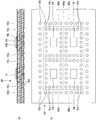
우선, 도 2의 (a) 및 도 2의 (b)에 나타낸 바와 같이, 상측 기판(20)을 형성하기 위한 상측 기판용 기판재(40)(이하, 기판재(40)라고 칭함)를 준비한다. 도 2의 (a)는 기판재(40)의 단면도이다. 도 2의 (b)는 기판재(40)의 이면을 나타낸 평면도이다. 기판재(40)는 복수 매(본 실시형태에서는 4매)의 상측 기판(20)을 형성하기 위한 1매의 재료이다. 4매의 상측 기판에 상당하는 영역(40b)이 기판재(40)의 중앙 부분에 정렬하고, 그 주위에 더미부(30)를 형성하기 위한 연장부(40a)가 연장해 있다.First, as shown in FIG.2 (a) and FIG.2 (b), the upper substrate substrate material 40 (henceforth a substrate material 40) for forming the
즉, 1매의 기판재(40)는, 점선으로 도시하는 바와 같이 4매 상측 기판(20)에 상당하는 영역(40b)을 포함하고, 영역(40b)으로부터 프레임 형상의 연장부(40a)가 연장해 있다. 기판재(40)의 이면에 있어서, 상측 기판(20)에 상당하는 영역(40b)에는 접합 패드(20b)가 형성되어 있다. 한편, 연장부(40a)에는 더미 볼(32)이 접합되는 접합 패드(20d)가 형성되어 있다. 기판재(40)의 표면에서 영역(40b)에는, 부품 접속 패드(20a)가 형성되어 있다.That is, one board |
반도체 패키지(10)에 설치되게 되는 부품 접속 패드(20a) 및 접합 패드(20b)는 배선 패턴에 접속되어 있지만, 더미부(30)로 형성되는 연장부(40a)에 배치되어 있는 접합 패드(20d)는 배선 패턴에 접속되지 않고, 서로 독립해 있는 것이 바람직하다. 즉, 접합 패드(20d)는 전기적 접속을 달성하는데 이용되지 않기 때문에, 배선 패턴을 접합 패드(20d)에 접속할 필요는 없다. 그러나, 연장부(40a)에 배치되어 있는 접합 패드(20d)는, 접합 패드(20b) 등과 같이 전기적으로 기능하는 부분에 접속되지 않는다면, 접합 패드(20d)끼리 연결되어 있어도 된다.Although the
도 2의 (a) 및 도 2의 (b)에 나타낸 기판재(40)를 준비한 후, 도 3의 (a) 및 도 3의 (b)에 나타낸 바와 같이, 상측 기판(20)의 이면의 접합 패드(20b) 및 접합 패드(20d) 상에 플럭스(42)를 도포한다. 도 3의 (a)는 기판재(40)의 단면도이고, 도 3의 (b)는 기판재(40)의 이면을 나타낸 평면도이다. 플럭스(42)는 땜납 접합을 용이하게 하기 위해 설치된다.After preparing the board |
계속해서, 도 4의 (a) 및 도 4의 (b)에 나타낸 바와 같이, 기판재(40)의 연장부(40a)의 이면의 접합 패드(20d) 상에 더미 볼(32)을 탑재한다. 도 4의 (a)는 기판재(40)의 단면도이다. 도 4의 (b)는 기판재(40)의 이면을 나타낸 평면도이다. 제 2 코어 포함 땜납 볼로서의 더미 볼(32)은 동 코어 볼(18)의 주위에 땜납(18a)을 설치함으로써 형성된다. 더미 볼(32)의 땜납(18a)의 양은 비교적 많고, 기판재(40)의 접합 패드(20d)와 후술하는 하측 기판용 기판재의 접합 패드를 땜납 접합하는데 충분한 양이다.Subsequently, as shown in FIGS. 4A and 4B, the
다음으로, 도 5의 (a) 및 도 5의 (b)에 나타낸 바와 같이, 기판재(40)의 이면의 영역(40b)에 설치되어 있는 접합 패드(20b) 상에 동 코어 땜납 볼(34)을 탑재한다. 도 5의 (a)는 기판재(40)의 단면도이다. 도 5의 (b)는 기판재(40)의 이면을 나타낸 평면도이다. 제 1 코어 포함 땜납 볼로서의 동 코어 땜납 볼(34)은, 상술한 바와 같이 동 코어 볼(18)의 주위에 땜납(18a)을 설치함으로써 형성된다. 동 코어 땜납 볼(34)의 땜납(18a)의 양은 미량이며, 기판재(40)의 접합 패드(20b)에 동 코어 볼(18)을 땜납 접합할 수 있으면 될 만큼의 양이다.Next, as shown to FIG. 5A and FIG. 5B, the copper
상술한 바와 같이, 상측 기판(12)을 형성하기 위한 상측 기판용 기판재(40)의 준비가 완료된다.As described above, the preparation of the upper
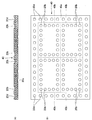
다음으로, 하측 기판(12)을 형성하기 위한 하측 기판용 기판재(50)(이하, 기판재(50)라고 칭함)의 준비에 대해서, 도 6의 (a) 및 도 6의 (b) 및 도 7의 (a) 및 도 7의 (b)을 참조하여 설명한다.Next, with respect to preparation of the lower substrate substrate material 50 (hereinafter referred to as the substrate material 50) for forming the
도 6의 (a)는 기판재(50)의 단면도이다. 도 6의 (b)는 기판재(50)의 표면을 나타낸 평면도이다. 기판재(50)는 복수 매의 하측 기판(12)을 형성하기 위한 1매의 재료이다. 도 6의 (a) 및 도 6의 (b)에서는, 4매의 하측 기판(12)에 상당하는 영역(50b)이 기판재(50)의 중앙 부분에 정렬하고, 영역(50b)의 주위에 더미부(30)를 형성하기 위한 연장부(50a)가 연장해 있다. 4개의 영역(50b)은 각각 상술한 기판재(40)의 4개의 영역(40b)에 대응해 있다. 도 6의 (a) 및 도 6의 (b)에서는, 4개의 영역(50b)이 형성된 부분만 나타나 있다. 그러나, 도 6의 (a) 및 도 6의 (b)에 나타낸 부분은 기판재(50)의 일부여도 되고, 기판재(50)는 벨트 형상과 같이 길게 이어져 있어도 되고, 4개의 영역(50b)의 집합이 벨트 형상의 기판재(50)를 따라 연속해서 배치되어 있는 것으로 해도 된다. 또한, 기판재(50)의 연장부(50a)는, 기판재(50)와 조합되는 기판재(40)의 연장부(40a)보다 큰 것이 바람직하다. 기판재(40)의 연장부(40a)보다 기판재(50)의 연장부(50a)를 크게 함으로써, 연장부(50a)의 외측 가장자리 부분에, 기판재(50)의 반송시에 이용되는 위치 결정 구멍 등을 형성해 둘 수 있다.6A is a sectional view of the
상술한 바와 같이, 1매의 기판재(50)는, 도 6의 (b)에 있어서 점선으로 나타낸 바와 같이 4매의 하측 기판(12)에 상당하는 영역(50b)을 포함하고, 영역(50b)의 주위에 프레임 형상의 연장부(50a)가 연장해 있다. 기판재(50)의 표면에 있어서, 상측 기판(12)에 상당하는 영역(50b)에는 접합 패드(12c)가 형성되어 있다. 기판재(50)의 표면에서 각각의 영역(50b)의 중앙 부분에는, 반도체 소자(14)의 전극 단자가 접속되는 전극 접속 패드(12b)가 형성되어 있다. 한편, 연장부(50a)의 표면측에는, 더미 볼(32)이 접합되는 접합 패드(12d)가 형성되어 있다.As mentioned above, one board |
또한, 반도체 패키지(10)에 설치되게 되는 접합 패드(12c)는 배선 패턴에 접속되어 있지만, 더미부(30)로 형성되는 연장부(50a)에 배치되어 있는 접합 패드(12d)는 배선 패턴에 접속되어 있지 않고, 서로 독립해 있다. 즉, 접합 패드(12d)는 전기적 접속을 목적으로 하는 것이 아니기 때문에, 배선 패턴 등과 접속할 필요는 없다. 그러나, 연장부(50a)에 배치되어 있는 접합 패드(12c)는, 접합 패드(12b) 등과 같이 전기적으로 기능하는 부분에 접속되지 않는다면, 접합 패드(12c)끼리 연결되어 있어도 된다.In addition, although the
이상과 같은 구성의 기판재(50)의 표면의 영역(50b)의 각각에, 도 6의 (a) 및 도 6의 (b)에 나타낸 바와 같이 반도체 소자(14)를 플립 칩 실장한다. 즉, 반도체 소자(14)의 전극을, 기판재(50)의 표면의 영역(50b)의 각각에 형성된 전극 접속 패드(12b)에 접합하고, 반도체 소자(14)와 기판재(50) 사이에 언더필재(14a)를 충전해서 반도체 소자(14)를 기판재(50)에 고정한다.The
반도체 소자(14)를 기판재(50)의 각 영역(50b)에 실장한 후, 도 7의 (a) 및 도 7의 (b)에 나타낸 바와 같이 연장부(50a)의 표면에 형성되어 있는 접합 패드(20d)(더미 볼(32)이 접합되는 패드)에 플럭스(52)를 도포한다. 도 7의 (a)는 기판재(50)의 단면도이고, 도 7의 (b)는 기판재(50)의 표면을 나타낸 평면도이다.After mounting the
상술한 공정에서, 하측 기판용 기판재(50)의 준비가 완료된다.In the above-described process, preparation of the lower
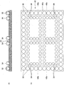
다음으로, 도 8의 (a) 및 도 8의 (b)에 나타낸 바와 같이, 이렇게 준비한 하측 기판용 기판재(50) 상에, 상술한 공정에 따라 준비한 상측 기판용 기판재(40)를 탑재한다. 기판재(50)의 4개의 영역(50b)과 기판재(40)의 4개의 영역(40b)이 각각 상하로 정렬하는 위치에 기판재(40)를 배치한다. 따라서, 상측 기판용 기판재(40)의 연장부(40a)에 형성된 접합 패드(20d)에 접합된 더미 볼(32)은, 하측 기판용 기판재(50)의 연장부(50a)에 형성된 접합 패드(12d) 상에 배치된다. 따라서, 상측 기판용 기판재(40)의 영역(40b)에 형성된 접합 패드(20b)에 접합된 동 코어 땜납 볼(34)은, 하측 기판용 기판재(50)의 영역(50b)에 형성된 접합 패드(12c) 상에 각각 배치되게 된다. 도 8의 (a)는 기판재(40)와 기판재(50)의 단면도이다. 도 8의 (b)는 기판재(40)가 탑재된 기판재(50)의 표면을 나타낸 평면도이다. 또한, 도 8의 (b)에 있어서, 기판재(40) 내부에, 기판재(40)의 하측에 위치되는 더미 볼(32), 동 코어 땜납 볼(34)과 반도체 소자(14)가 점선으로 나타내져 있다.Next, as shown to Fig.8 (a) and FIG.8 (b), the upper board |
도 8의 (a)에 나타낸 바와 같이, 기판재(40)는, 더미 볼(32)과 동 코어 땜납 볼(34)을 기판재(50)와 기판재(40) 사이에 끼운 상태로 기판재(50) 상에 배치되어, 기판재(50)와 기판재(40) 사이에는 더미 볼(32)과 동 코어 땜납 볼(34)에 의하여 간극이 형성된다. 각 영역(50b)에 탑재된 반도체 소자(14)는, 기판재(50)와 기판재(40) 사이의 간극 내에 수용된다.As shown in FIG. 8A, the
그리고, 이렇게 조합된 기판재(50)와 기판재(40)를 리플로우 노(爐)에서 가열한다. 이에 의해, 더미 볼(32)이 땜납(18a)이 용융해서, 기판재(40)의 접합 패드(20d)와 기판재(50)의 접합 패드(12d)가 서로 땜납 접합된다. 이 때, 동 코어 땜납 볼(34)의 땜납도 용융한다. 그러나, 동 코어 땜납 볼(34)의 땜납의 양이 적기 때문에, 용융한 땜납은 기판재(40)의 접합 패드(20b)와 동 코어 볼(18) 사이의 위치에 유지되고, 기판재(50)의 접합 패드(12c)로는 이동하지 않는다. 따라서, 동 코어 땜납 볼(34)이 개재(介在)해 있는 부분에서는, 동 코어 볼(18)은 접합 패드(12c)에 땜납 접합되지 않고, 접합 패드(12c)에 압접한 상태로 된다. 한편, 더미 볼(32)이 개재해 있는 부분에서는, 땜납의 양이 많기 때문에, 용융된 땜납이 동 코어 볼(18)의 표면을 따라 흘러 접합 패드(12c)와 접합 패드(20b)로 이동하여, 접합 패드(12d)와 접합 패드(20b)를 각각 땜납 접합된다.And the board |
기판재(40)를 기판재(50)에 대하여 가압하면서 땜납 리플로우가 행해지지만, 더미 볼(32)의 동 코어 볼(18)과 동 코어 땜납 볼(34)의 동 코어 볼(18)이 스페이서 부재로서 기능하기 때문에, 기판재(40)와 기판재(50) 사이의 간격은 소정의 거리로 유지된다. 더미 볼(32)의 동 코어 볼(18)과 동 코어 땜납 볼(34)의 동 코어 볼(18)은 동일한 동 코어 볼이며, 그 외경은 서로 동일하다. 이 때문에, 기판재(40)의 이면과 기판재(50) 표면 사이의 거리를 전체적으로 균일하게 할 수 있다.Solder reflow is performed while pressing the
상술한 바와 같이, 기판재(40)를 기판재(50)에 고정한다. 즉, 기판재(40)의 연장부(40b)와 기판재(50)의 연장부(50b) 사이에 있어서, 접합 패드(20d)와 접합 패드(12d)가 더미 볼(32)의 땜납(18a)에 의해 땜납 접합되기 때문에, 기판재(40)를 기판재(50)에 확실하게 고정할 수 있다. 이 상태에서, 기판재(40)가 고정된 기판재(50)를 수지 밀봉 장치까지 옮긴다. 기판재(40)는 얇아 깨지기 쉽지만 기판재(50)에 고정되어 있기 때문에, 기판 깨짐 등의 문제 없이, 용이하게 취급 및 옮길 수 있다.As described above, the
수지 밀봉 장치에 있어서, 도 9에 나타낸 바와 같이, 기판재(40)가 고정된 기판재(50)를 상하 금형(60A, 60B)에 의해 클램핑하고, 기판재(40)와 기판재(50) 사이에 몰드 수지(22)를 주입한다. 상측 금형(60A)에 의해 기판재(40)를 기판재(50)에 대하여 가압하면서 몰드 수지(22)를 주입하고 경화시킨다. 몰드 수지(22)가 경화해서 밀봉 수지부(64)가 형성된다. 도 9에 나타낸 바와 같이, 반도체 소자(14)는 밀봉 수지부(64) 중에 메워넣어지고, 더미 볼(32) 및 동 코어 땜납 볼(34)도 밀봉 수지부(64) 내에 메워넣어진다. 이 상태에서, 밀봉 수지부(64)의 접착력으로 인해, 동 코어 땜납 볼(34)의 동 코어 볼(18)은, 기판재(50)의 접합 패드(12c)에 압접(壓接)된 상태로 된다. 이에 따라, 기판재(40)의 접합 패드(20b)는 동 코어 볼(18)을 통해 기판재(50)의 접합 패드(12c)에 확실하게 전기적으로 접속된다.In the resin sealing device, as shown in FIG. 9, the
또한, 본 실시형태에 따르면, 동 코어 땜납 볼(34)이 땜납(18a) 양은, 리플로우에 의해 용융해도 기판재(50)의 접합 패드(12d)까지 흐르지 않는 정도의 양으로 설정했지만, 미량의 땜납이 접합 패드(12d)까지 흐르는 정도로 땜납 양을 설정해도 된다. 이 경우, 동 코어 볼(18)은 접합 패드(12d)에도 땜납 접합되게 되지만, 더미 볼(32)의 땜납 양보다 동 코어 땜납 볼(34)의 땜납의 양을 적게 함으로써 밀봉 수지부(64) 내에 메워넣어져도 문제를 야기하지 않도록 할 수 있다.In addition, according to this embodiment, although the amount of the
주입한 몰드 수지(22)가 경화해서 밀봉 수지부(64)가 형성된 후, 상하 금형(60A, 60B)을 열고, 기판재(50)를 취출한다. 그리고, 도 10에 나타낸 바와 같이, 기판재(50)의 이면의 외부 접속 패드(12a)에 땜납 볼을 설치하고, 땜납 볼을 리플로우해서 외부 접속 단자로서 땜납 범프(66)를 형성한다.After the injected
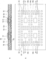
도 10에 나타낸 상태에 있어서, 상측 기판용 기판재(40)의 4개의 영역(40b)과 하측 기판용 기판재(50)의 4개의 영역(50b)에 의해, 4개의 반도체 패키지가 밀봉 수지부(64)에 의해 연결되어서 형성되어 있다. 그리고, 4개의 반도체 패키지의 주위에는 더미부(30)가 형성되어 있다.In the state shown in FIG. 10, the four semiconductor packages are sealed by the four
그 후, 더미부(30)를 4개의 반도체 패키지(10)로부터 분리하고, 또한 4개의 반도체 패키지(10)를 분리해서 개편화한다. 즉, 도 11에 나타낸 바와 같이, 우선 더미부(30)와 반도체 패키지(10) 사이의 라인(영역(40b)과 연장부(40a) 사이의 경계에 상당함)을 따라 다이싱에 의해 절단해서 더미부(30)를 제거한다. 기판재(40)와 기판재(50)는, 밀봉 수지부(64)에 의해 강고하게 고정되어 있으므로, 더미부(30)를 절단해도 떨어지지 않는다. 그 후, 4개의 반도체 패키지(10) 사이의 라인(4개의 영역(40b) 사이의 경계)을 따라 다이싱에 의해 절단함으로써, 도 11의 (a) 및 도 11의 (b)에 나타낸 바와 같이 반도체 패키지(10)를 개편화한다.Thereafter, the
이상의 공정에 따라, 4개의 반도체 패키지(10)를 일괄해서 제조할 수 있다. 일괄해서 제조하는 반도체 패키지(10)의 수는 4개로 한정하지 않고, 상측 기판재(40)와 하측 기판재(50)를 준비하는 범위 내에서, 임의의 수의 반도체 패키지를 일괄해서 제조할 수 있다.According to the above process, four
이상 설명한 제조 방법에 의해 제조한 반도체 패키지(10)에 있어서, 상측 기판(20)과 하측 기판(12) 사이에 몰드 수지(22)가 충전되어, 상측 기판(20)은 하측 기판(12)에 대하여 고정된다. 상측 기판(20)과 하측 기판(12) 사이의 거리는 동 코어 볼(18)에 의해 유지되어 있다. 상술한 바와 같이, 본 실시형태에 따르면, 다량의 땜납을 갖는 더미 볼(32)이 설치된 더미부(30)는 제거되므로, 밀봉 수지부(64) 내에 가둬지는 땜납은 소량이다. 그러므로, 밀봉 수지부(64) 내의 땜납이 용융해서 열팽창해도, 밀봉 수지부(64)와 배선 패턴 사이에 용융한 땜납이 진입하지 않고, 진입해도 그 땜납의 양은 매우 적어서, 단락 등의 문제를 야기하지 않는다.In the
또한, 본 실시형태에 있어서, 동으로 형성된 동 코어 볼(18)을 스페이서 부재로 기능하는 도전성 코어 볼로서 이용하고 있지만, 도전성 코어 볼의 재료는 동에 한정되지 않는다. 예를 들면, 동 코어 볼(18) 대신에 금이나 니켈 등의 금속에 의해 형성한 도전성 코어 볼을 이용해도 된다. 또한, 더미 볼(32)에 사용하는 동 코어 볼(18)은, 반드시 동 코어 땜납 볼(34)에 사용하는 동 코어 볼(18)과 동일한 것은 아니다. 더미 볼(32)에 사용하는 동 코어 볼(18)은 전기적 접속하는데 사용되지 않기 때문에, 저저항일 필요는 없다. 그러므로, 더미 볼(32)에 사용되는 동 코어 볼(18)은 니켈 등의 다른 금속으로 형성한 도전성 코어 볼일 수 있고, 혹은 세라믹스 등으로 형성한 비도전성 코어 볼(단순한 코어 볼)일 수 있다.In addition, in this embodiment, although the
본 실시형태에서는, 더미 볼(32)을 미리 상측 기판용 기판재(40)의 접합 패드(20d)에 접합하고 나서 기판재(40)를 기판재(50)에 부착함으로써, 더미 볼(32)을 기판재(40)와 기판재(50) 사이에 배치하고 있다. 그러나, 더미 볼(32)을 미리 하측 기판용 기판재(50)의 접합 패드(12d)에 접합해도 된다.In the present embodiment, the
다음으로, 제 2 실시형태에 따른 반도체 패키지의 제조 방법에 관하여 설명한다.Next, the manufacturing method of the semiconductor package which concerns on 2nd Embodiment is demonstrated.
제 2 실시형태에 따른 반도체 패키지에서는, 제 1 실시형태에 따른 더미 볼(32) 및 동 코어 땜납 볼(34) 대신에, 땜납(18a)을 설치하지 않은 동 코어 볼(18)을 이용한다. 그러므로, 예를 들면 은 페이스트나 동 페이스트 등의 도전성 페이스트(접합재)에 의해 동 코어 볼(18)을 접합 패드에 접합한다. 도전성 페이스트를 동 코어 볼(18)의 주위에 설치하지 않고, 접합 패드에 도포해 둘 수 있다.In the semiconductor package according to the second embodiment, instead of the
우선, 제 1 실시형태와 마찬가지로, 도 12의 (a) 및 도 12의 (b)에 나타낸 바와 같이, 상측 기판(20)을 형성하기 위한 상측 기판용 기판재(40)(이하, 기판재(40)라고 칭함)를 준비한다. 도 12의 (a)는 기판재(40)의 단면도이다. 도 12의 (b)는 기판재(40)의 이면을 나타낸 평면도이다. 이하의 설명에 있어서, 상술한 제 1 실시형태에 있어서의 구성 부품과 동등한 구성 부품에는 동일한 부호를 부여하고, 그 설명을 생략한다. 또한, 제 1 실시형태에 있어서의 제조 공정과 동등한 제조 공정의 설명을 생략한다.First, as in the first embodiment, as shown in FIGS. 12A and 12B, the
도 12의 (a) 및 도 12의 (b)에 나타낸 기판재(40)를 준비한 후, 도 13의 (a) 및 도 13의 (b)에 나타낸 바와 같이 기판재(40)의 이면의 접합 패드(20b) 및 접합 패드(20d) 상에 도전성 페이스트(72)를 도포한다. 도 13의 (a)는 기판재(40)의 단면도이다. 도 13의 (b)는 기판재(40)의 이면을 나타낸 평면도이다. 도전성 페이스트(72)는 동 코어 볼(18)을 접합하기 위해서 설치된다.After preparing the board |
계속해서, 도 14의 (a) 및 도 14의 (b)에 나타낸 바와 같이, 기판재(40)의 접합 패드(20d) 및 접합 패드(20b) 상에 각각 설치된 도전성 페이스트(72) 상에 동 코어 볼(18)을 배치한다. 도전성 페이스트(72)를 상온 또는 가열 경화시킴으로써, 동 코어 볼(18)은 도전성 페이스트(72)에 의해 접합 패드(20d) 및 접합 패드(20b)에 접합된다. 또한, 도 14의 (a)는 기판재(40)의 단면도이다. 도 14의 (b)는 기판재(40)의 이면을 나타낸 평면도이다.Subsequently, as shown in Figs. 14A and 14B, the copper paste is formed on the
이상에 따라, 상측 기판(20)을 형성하는데 이용되는 상측 기판용 기판재(40)의 준비가 완료된다.According to the above, preparation of the upper
다음으로, 하측 기판(12)을 형성하기 위한 하측 기판용 기판재(50)(이하, 기판재(50)라고 칭함)의 준비에 대해서, 도 15의 (a), 도 15의 (b), 도 16의 (a) 및 도 16의 (b)를 참조하여 설명한다.Next, with respect to preparation of the lower substrate substrate material 50 (hereinafter referred to as the substrate material 50) for forming the
도 15의 (a)는 기판재(50)의 단면도이다. 도 15의 (b)는 기판재(50)의 표면을 나타낸 평면도이다. 우선, 도 15의 (a) 및 도 15의 (b)에 나타낸 바와 같이, 기판재(50)에 반도체 소자(14)를 플립 칩 실장하고, 반도체 소자(14)와 기판재(50) 사이에 각각 언더필재(14a)를 충전해서 반도체 소자(14)를 기판재(50)에 고정한다.15A is a cross-sectional view of the
반도체 소자(14)를 기판재(50)의 각 영역(50b)에 실장한 후, 연장부(50a)의 표면에 형성되어 있는 접합 패드(20d)에 페이스트(74)를 도포한다. 도 16의 (a)는 기판재(50)의 단면도이다. 도 16의 (b)는 기판재(50)의 표면을 나타낸 평면도이다.After mounting the
이상에 따르면, 하측 기판용 기판재(50)의 준비가 완료한다.According to the above, preparation of the board |
다음으로, 도 17의 (a) 및 도 17의 (b)에 나타낸 바와 같이, 이렇게 준비한 하측 기판용 기판재(50) 상에, 상술한 바와 같은 공정에 따라 준비한 상측 기판용 기판재(40)를 탑재한다. 기판재(50)의 4개의 영역(50b)과 기판재(40)의 4개의 영역(40b)이 각각 상하로 정렬하는 위치에 기판재(40)를 배치한다. 따라서, 상측 기판용 기판재(40)의 연장부(40b)에 형성된 접합 패드(20d)에 접합된 동 코어 볼(18)은, 하측 기판용 기판재(50)의 연장부(50a)에 형성된 접합 패드(12d) 상에 배치된다. 따라서, 상측 기판용 기판재(40)의 영역(40b)에 형성된 접합 패드(20b)에 접합된 동 코어 볼(18)은, 하측 기판용 기판재(50)의 영역(50b)에 형성된 접합 패드(12c) 상에 각각 배치되게 된다. 또한, 도 17의 (a)는 기판재(40)와 기판재(50)의 단면도이다. 도 17의 (b)는 기판재(40)가 탑재된 기판재(50)의 표면을 나타낸 평면도이다. 또한, 도 17의 (b)에 있어서, 기판재(40)의 하측에 있는 동 코어 볼(18)과 반도체 소자(14)가 기판재(40) 내부에 점선으로 나타나 있다.Next, as shown to Fig.17 (a) and FIG.17 (b), on the lower
도 17의 (a)에 나타낸 바와 같이, 기판재(40)는, 기판재(50)와 기판재(40) 사이에 동 코어 볼(18)을 끼운 상태로 기판재(50) 상에 배치되어서, 기판재(50)와 기판재(40) 사이에는 동 코어 볼(18)로 인해 간극이 형성된다. 각 영역(50)에 탑재된 반도체 소자(14)는 기판재(50)와 기판재(40) 사이의 간극 내에 수용된다.As shown in FIG. 17A, the
그리고, 이렇게 조합된 기판재(50)와 기판재(40)를 리플로우 노에서 가열한다. 이에 의해, 접합 패드(12d) 상의 땜납 페이스트(74)가 용융하여, 기판재(50)의 접합 패드(12d)와 동 코어 볼(18)이 서로 땜납 접합된다. 접합 패드(12d)에 땜납 접합된 동 코어 볼(18)은, 기판재(40)를 준비하는 단계에서 기판재(40)의 접합 패드(20d)에 도전성 페이스트(72)에 의해 접합되어 있으므로, 기판재(40)의 접합 패드(20d)와 기판재(50)의 접합 패드(12d)는 동 코어 볼(18)을 통해 서로 접합된다. 따라서, 기판재(40)는 기판재(50)에 고정된다.The
그 후, 상술한 제 1 실시형태와 마찬가지로, 수지 밀봉 장치에 있어서, 도 18에 나타낸 바와 같이, 기판재(40)가 고정된 기판재(50)를 상하 금형(60A, 60B)에 의해 클램핑하고, 기판재(40)와 기판재(50) 사이에 몰드 수지(22)를 주입한다. 상측 금형(60A)에 의해 기판재(40)를 기판재(50)에 대하여 가압하면서 몰드 수지(22)를 주입하고 경화시킨다. 몰드 수지(22)가 경화해서 밀봉 수지부(64)가 형성된다. 도 18에 나타낸 바와 같이, 반도체 소자(14)는 밀봉 수지부(64) 내에 메워넣어지고, 또한 동 코어 볼(18)도 밀봉 수지부(64) 중에 메워넣어진다. 이 상태에서, 밀봉 수지부(64)의 접착력으로 인해, 상측 기판(40)의 접합 패드(20b)에 접합된 동 코어 볼(18)은, 기판재(50)의 접합 패드(12c)에 압접된다. 이에 의해, 기판재(40)의 접합 패드(20b)는 동 코어 볼(18)을 통해 기판재(50)의 접합 패드(12c)에 확실하게 전기적으로 접속된다.Thereafter, in the resin sealing device, as shown in FIG. 18, the
주입한 몰드 수지(22)가 경화해서 밀봉 수지부(64)가 형성된 후, 상하 금형(60A, 60B)을 열고, 기판재(50)를 취출한다. 그리고, 도 19에 나타낸 바와 같이, 기판재(50)의 이면의 외부 접속 패드(12a)에 땜납 볼을 설치하고, 땜납 볼을 리플로우해서 외부 접속 단자로서 범프(66)를 형성한다.After the injected
도 19에 나타낸 상태에 있어서, 상측 기판용 기판재(40)의 4개의 영역(40b)과 하측 기판용 기판재(50)의 4개의 영역(50b)에 의해, 4개의 반도체 패키지가 밀봉 수지부(64)에 의해 연결되어서 형성된다. 4개의 반도체 패키지의 주위에는 더미부(30)가 형성되어 있다.In the state shown in FIG. 19, four semiconductor packages are sealed by the four
그리고, 4개의 반도체 패키지(80)로부터 더미부(30)를 분리하고, 또한 이들 4개의 반도체 패키지(10)를 개편화한다. 즉, 도 20에 나타낸 바와 같이, 우선 더미부(30)와 반도체 패키지(80) 사이의 라인(영역(40b)과 연장부(40a) 사이의 경계에 상당함)을 다이싱에 의해 절단해서 더미부(30)를 제거한다. 기판재(40)와 기판재(50)는, 밀봉 수지부(64)에 의해 강고하게 고정되어 있으므로, 더미부(30)를 절단해도 떨어지지 않는다. 그 후, 4개의 반도체 패키지(10)의 사이의 라인(4개의 영역(40b) 사이의 경계)을 따라 다이싱에 의해 절단함으로써, 도 20의 (a) 및 도 20의 (b)에 나타낸 바와 같이 반도체 패키지(80)를 개편화한다.And the
이상의 공정에 따라, 4개의 반도체 패키지(80)를 일괄해서 제조할 수 있다. 일괄해서 제조하는 반도체 패키지(80)의 수는 4개로 한정되지 않고, 상측 기판(40)과 하측 기판(50)의 준비 범위 내에서, 임의의 수의 반도체 패키지를 일괄해서 제조할 수 있다.According to the above process, four
이상에서 설명한 제조 방법에 의해 제조한 반도체 패키지(80)에 있어서, 상측 기판(20)과 하측 기판(12) 사이에 몰드 수지가 충전되어, 상측 기판(20)은 하측 기판(12)에 대하여 고정된다. 상측 기판(20)과 하측 기판(12) 사이의 거리는 동 코어 볼(18)에 의해 유지된다. 상술한 바와 같이, 본 실시형태에 따르면, 반도체 패키지(80)의 밀봉 수지(64) 내에 땜납이 설치되지 않기 때문에, 밀봉 수지부(64)와 배선 패턴 사이에 용융한 땜납이 진입하지 않아, 밀봉 수지부(64) 내의 땜납에 기인한 문제가 생기지 않는다.In the
또한, 본 실시형태에 있어서도, 동으로 형성된 동 코어 볼(18)을 스페이서 부재로서 기능하는 도전성 코어 볼로서 사용하고 있지만, 도전성 코어 볼의 재료는 동에 한정되지 않는다. 예를 들면, 동 코어 볼(18) 대신에, 금이나 니켈 등의 금속으로 형성한 도전성 코어 볼을 이용해도 된다. 또한, 더미부(30)에 사용되는 동 코어 볼(18)은, 반드시 반도체 패키지(80)에 사용하는 동 코어 볼(18)과 동일할 필요는 없다. 더미부(30)에 설치되는 동 코어 볼(18)은 전기적 접속을 위해 사용되지 않기 때문에, 저저항일 필요는 없다. 그러므로, 더미부(30)에 사용되는 동 코어 볼(18)은 니켈 등의 다른 금속으로 형성한 도전성 코어 볼일 수 있고, 또는 세라믹스 등으로 형성한 비도전성 코어 볼(단순한 코어 볼)일 수 있다.In addition, in this embodiment, although the
모든 예들과 여기에서 인용된 조건부 언어는 교시적 목적으로, 본 발명자가 종래 기술을 발전시키기 위해 제공한 본 발명의 원리 및 개념의 독자의 이해를 돕기 위함이어서, 구체적으로 인용된 이러한 예들과 조건으로의 제약이 없는 것으로 이해될 것이며, 명세서의 이러한 예들의 구성은 본 발명의 우열을 나타내는 것에 관한 것은 아니다. 본 발명의 실시형태를 상세하게 기술했지만, 본 발명의 사상과 범주에서 벗어나지 않고 그 내에서 다양한 변경, 치환, 및 교체가 이루어질 수 있음을 이해할 것이다.All examples and conditional languages cited herein are for teaching purposes and are intended to assist the reader in understanding the principles and concepts of the present invention provided by the inventors for the development of the prior art, and are specifically cited in these examples and conditions. It is to be understood that there is no limitation, and the configuration of these examples in the specification is not intended to represent the superiority of the present invention. While embodiments of the invention have been described in detail, it will be understood that various changes, substitutions, and substitutions can be made therein without departing from the spirit and scope of the invention.
10 반도체 패키지 12 하측 기판
12a 외부 접속 패드 12b 전극 접속 패드
12c 접합 패드 14 반도체 소자
14a 언더필재 17 솔더레지스트
18 동 코어 볼 18a 땜납
20 상측 기판 20a 부품 접속 패드
20b 접합 패드 20d 접합 패드
22 몰드 수지 30 더미부
32 더미 볼 34 동 코어 땜납 볼
40 상측 기판용 기판재 40a 연장부
40b 영역 50 하측 기판용 기판재
50a 연장부 50b 영역
64 밀봉 수지부 66 땜납 범프
72 도전성 페이스트 74 땜납 페이스트10
12a
18
20
22
32
64
72
Claims (6)
상기 상측 기판 및 상기 상측 기판의 주위의 연장부를 포함하는 상측 기판용 기판재를 준비하고, 상기 상측 기판에 형성된 접합 패드에 상기 스페이서 부재로서 도전성 코어 볼을 접합하고 또한 상기 연장부에 형성된 접합 패드에 코어 볼을 접합함과 함께, 상기 하측 기판 및 상기 하측 기판의 주위의 연장부를 포함하는 하측 기판용 기판재를 준비하는 단계와,
상기 상측 기판용 기판재의 연장부에 형성된 접합 패드를 상기 코어 볼을 통해 상기 하측 기판용 기판재의 연장부에 형성된 접합 패드에 접합하고, 또한 상기 상측 기판용 기판재의 상기 상측 기판에 상당하는 영역에 형성된 접합 패드를 상기 코어 볼 및 상기 도전성 코어 볼을 통해 상기 하측 기판용 기판재의 상기 하측 기판에 상당하는 영역에 형성된 접합 패드에 전기적으로 접속함으로써, 상기 상측 기판용 기판재를 상기 하측 기판용 기판재에 접속하는 단계와,
상기 상측 기판용 기판재와 상기 하측 기판용 기판재 사이에 몰드 수지를 충전함으로써, 상기 상측 기판용 기판재를 상기 하측 기판용 기판재에 고정하는 단계와,
상기 상측 기판용 기판재의 연장부와 상기 하측 기판용 기판재의 연장부를 포함하는 부분을 제거하는 단계와,
상기 반도체 패키지를 개편화(個片化)하는 단계를 포함하는 반도체 패키지의 제조 방법.An upper substrate and a lower substrate connected to each other through a spacer member, a semiconductor element disposed between the upper substrate and the lower substrate, and a mold filled in a space between the upper substrate and the lower substrate; As a manufacturing method of a semiconductor package which manufactures a plurality of semiconductor packages containing resin collectively,
An upper substrate substrate material including the upper substrate and an extension portion around the upper substrate is prepared, and a conductive core ball is bonded to the bonding pad formed on the upper substrate as the spacer member, and the bonding pad formed on the extension portion. Bonding a core ball and preparing a lower substrate substrate material including an extension portion around the lower substrate and the lower substrate;
Bonding pads formed in the extension portion of the upper substrate substrate material are bonded to bonding pads formed in the extension portion of the lower substrate substrate material through the core ball, and formed in a region corresponding to the upper substrate of the upper substrate substrate material. The bonding pad is electrically connected to the bonding pad formed in the region corresponding to the lower substrate of the lower substrate substrate material through the core ball and the conductive core ball to thereby connect the upper substrate substrate material to the lower substrate substrate material. Connecting,
Fixing the upper substrate substrate material to the lower substrate substrate material by filling a mold resin between the upper substrate substrate material and the lower substrate substrate material;
Removing a portion including an extension of the upper substrate material and an extension of the lower substrate material;
A method of manufacturing a semiconductor package comprising the step of separating the semiconductor package.
상기 상측 기판용 기판재 내의 상기 상측 기판에 상당하는 영역에 설치된 접합 패드에 상기 도전성 코어 볼을 접합하기 위한 땜납의 양을, 상기 상측 기판용 기판재의 연장부에 설치된 접합 패드에 상기 코어 볼을 접합하기 위한 땜납의 양보다 적게 하는 반도체 패키지의 제조 방법.The method of claim 1,
The core ball is bonded to a bonding pad provided on an extension of the upper substrate substrate material with an amount of solder for bonding the conductive core ball to a bonding pad provided in a region corresponding to the upper substrate in the upper substrate substrate material. A method for manufacturing a semiconductor package, which is less than the amount of solder to be used.
상기 상측 기판용 기판재 내의 상기 상측 기판에 상당하는 영역에 설치된 접합 패드에 상기 도전성 코어 볼을 접합하기 위해, 상기 도전성 코어 볼 및 상기 도전성 코어 볼의 외주에 설치된 땜납을 각각 포함하는 제 1 코어 포함 땜납 볼을 사용하고,
상기 상측 기판용 기판재의 연장부에 설치된 접합 패드에 상기 코어 볼을 접합하기 위해, 상기 코어 볼 및 상기 코어 볼의 외주에 설치된 땜납을 포함하는 제 2 코어 포함 땜납 볼을 사용하고,
상기 제 1 코어 포함 땜납 볼의 땜납의 양은, 상기 상측 기판용 기판재의 접합 패드에 상기 도전성 코어 볼을 땜납 접합할 수 있는 양으로 설정되고,
상기 제 2 코어 포함 땜납 볼의 땜납의 양은, 상기 하측 기판용 기판재의 접합 패드에 상기 코어 볼을 땜납 접합할 수 있는 양으로 설정되는 반도체 패키지의 제조 방법.The method of claim 2,
A first core each including a solder provided on an outer circumference of the conductive core ball and the conductive core ball so as to bond the conductive core ball to a bonding pad provided in a region corresponding to the upper substrate in the upper substrate substrate; Using solder balls,
In order to bond the said core ball to the bonding pad provided in the extension part of the said board | substrate material for upper sides, the 2nd core containing solder ball containing the said core ball and the solder provided in the outer periphery of the said core ball is used,
The amount of solder of the first core-containing solder ball is set to an amount capable of solder bonding the conductive core ball to a bonding pad of the upper substrate substrate material,
The amount of solder of the solder ball containing the second core is set to an amount capable of solder bonding the core ball to a bonding pad of the lower substrate substrate material.
상기 상측 기판용 기판재에 설치된 접합 패드에 상기 도전성 코어 볼 및 상기 코어 볼을 접합하기 위해 도전성 페이스트를 사용하고, 또한 상기 하측 기판용 기판재의 연장부에 설치된 접합 패드에 상기 코어 볼을 접합하기 위해 땜납 페이스트를 사용하는 반도체 패키지의 제조 방법.The method of claim 1,
To use the conductive paste to bond the conductive core ball and the core ball to the bonding pad provided on the upper substrate substrate material, and to bond the core ball to the bonding pad provided on the extension of the lower substrate substrate material A method for manufacturing a semiconductor package using solder paste.
상기 상측 기판용 기판재의 상기 상측 기판에 상당하는 영역에 설치된 접합 패드에 접합된 상기 도전성 코어 볼을, 상기 하측 기판용 기판재의 상기 하측 기판에 상당하는 영역에 설치된 접합 패드에 압접(壓接)시킨 상태에서, 상기 몰드 수지에 의해 상기 상측 기판용 기판재를 상기 하측 기판용 기판재에 고정하는 반도체 패키지의 제조 방법.The method of claim 1,
The conductive core ball bonded to a bonding pad provided in a region corresponding to the upper substrate of the upper substrate substrate material is press-welded to a bonding pad provided in a region corresponding to the lower substrate of the lower substrate substrate material. In the state, the manufacturing method of the semiconductor package which fixes the said upper substrate substrate material to the said lower substrate substrate material by the said mold resin.
상기 상측 기판용 기판재의 연장부와 상기 하측 기판용 기판재의 연장부를 포함하는 부분을 다이싱에 의해 절단해서 제거하는 반도체 패키지의 제조 방법.The method of claim 1,
The manufacturing method of the semiconductor package which cuts and removes the part containing the extension part of the said upper substrate material, and the extension part of the said lower substrate material by dicing.
Applications Claiming Priority (2)
| Application Number | Priority Date | Filing Date | Title |
|---|---|---|---|
| JP2010146769A JP5421863B2 (en) | 2010-06-28 | 2010-06-28 | Manufacturing method of semiconductor package |
| JPJP-P-2010-146769 | 2010-06-28 |
Related Child Applications (1)
| Application Number | Title | Priority Date | Filing Date |
|---|---|---|---|
| KR1020170140195A Division KR101827807B1 (en) | 2010-06-28 | 2017-10-26 | Manufacturing method of semiconductor packages |
Publications (1)
| Publication Number | Publication Date |
|---|---|
| KR20120001621A true KR20120001621A (en) | 2012-01-04 |
Family
ID=45352922
Family Applications (2)
| Application Number | Title | Priority Date | Filing Date |
|---|---|---|---|
| KR1020110060989A KR20120001621A (en) | 2010-06-28 | 2011-06-23 | Manufacturing method of semiconductor packages |
| KR1020170140195A KR101827807B1 (en) | 2010-06-28 | 2017-10-26 | Manufacturing method of semiconductor packages |
Family Applications After (1)
| Application Number | Title | Priority Date | Filing Date |
|---|---|---|---|
| KR1020170140195A KR101827807B1 (en) | 2010-06-28 | 2017-10-26 | Manufacturing method of semiconductor packages |
Country Status (3)
| Country | Link |
|---|---|
| US (1) | US8470643B2 (en) |
| JP (1) | JP5421863B2 (en) |
| KR (2) | KR20120001621A (en) |
Cited By (3)
| Publication number | Priority date | Publication date | Assignee | Title |
|---|---|---|---|---|
| KR20130086110A (en) * | 2012-01-23 | 2013-07-31 | 쿄세라 에스엘시 테크놀로지 가부시키가이샤 | Assembly of multi-pattern wiring substrate and method of assembling multi-pattern wiring substrate |
| KR20210150598A (en) * | 2017-06-20 | 2021-12-10 | 가부시키가이샤 무라타 세이사쿠쇼 | Module and method for producing same |
| US11664300B2 (en) | 2019-12-26 | 2023-05-30 | Taiwan Semiconductor Manufacturing Co., Ltd. | Fan-out packages and methods of forming the same |
Families Citing this family (12)
| Publication number | Priority date | Publication date | Assignee | Title |
|---|---|---|---|---|
| US8508045B2 (en) | 2011-03-03 | 2013-08-13 | Broadcom Corporation | Package 3D interconnection and method of making same |
| US9064781B2 (en) | 2011-03-03 | 2015-06-23 | Broadcom Corporation | Package 3D interconnection and method of making same |
| JP2013219170A (en) * | 2012-04-09 | 2013-10-24 | Yokogawa Electric Corp | Substrate device |
| US8809181B2 (en) * | 2012-11-07 | 2014-08-19 | Intel Corporation | Multi-solder techniques and configurations for integrated circuit package assembly |
| DE102013217301A1 (en) * | 2013-08-30 | 2015-03-05 | Robert Bosch Gmbh | component |
| WO2015079990A1 (en) * | 2013-11-26 | 2015-06-04 | 東レエンジニアリング株式会社 | Mounting device and mounting method |
| US20190067176A1 (en) * | 2016-03-22 | 2019-02-28 | Intel Corporation | Void reduction in solder joints using off-eutectic solder |
| US20190206821A1 (en) * | 2017-12-29 | 2019-07-04 | Intel Corporation | Substrate assembly with spacer element |
| CN111029296B (en) * | 2019-11-22 | 2022-11-22 | 中国电子科技集团公司第十三研究所 | Preparation method of multilayer substrate stacking structure with controllable stacking interval |
| JP6767665B1 (en) * | 2020-06-10 | 2020-10-14 | 千住金属工業株式会社 | How to form a bump electrode substrate |
| US11562936B2 (en) | 2020-08-31 | 2023-01-24 | Amkor Technology Singapore Holding Pte. Ltd. | Electrionic devices with interposer and redistribution layer |
| JP2022188977A (en) | 2021-06-10 | 2022-12-22 | 新光電気工業株式会社 | Semiconductor device and method for manufacturing semiconductor device |
Family Cites Families (16)
| Publication number | Priority date | Publication date | Assignee | Title |
|---|---|---|---|---|
| JP2002324952A (en) * | 2001-04-24 | 2002-11-08 | Denso Corp | Printed circuit board |
| JP2002368369A (en) * | 2001-06-06 | 2002-12-20 | Yamaichi Electronics Co Ltd | Flexible printed wiring board and its manufacturing method |
| JP3507819B2 (en) * | 2001-10-29 | 2004-03-15 | 松下電器産業株式会社 | Resin-sealed semiconductor device and method of manufacturing the same |
| JP2004134482A (en) * | 2002-10-09 | 2004-04-30 | Toppan Printing Co Ltd | Method of manufacturing multilayer printed wiring board |
| JP2005085825A (en) * | 2003-09-04 | 2005-03-31 | Sony Corp | Structure of connection between bare chip and board, and bare chip socket |
| JP2006049569A (en) * | 2004-08-04 | 2006-02-16 | Sharp Corp | Stacked semiconductor-device package and manufacturing method therefor |
| JP4182144B2 (en) * | 2005-12-14 | 2008-11-19 | 新光電気工業株式会社 | Manufacturing method of chip embedded substrate |
| EP1962342A4 (en) | 2005-12-14 | 2010-09-01 | Shinko Electric Ind Co | Substrate with built-in chip and method for manufacturing substrate with built-in chip |
| US20080029879A1 (en) * | 2006-03-01 | 2008-02-07 | Tessera, Inc. | Structure and method of making lidded chips |
| JP4949114B2 (en) * | 2007-04-11 | 2012-06-06 | 新光電気工業株式会社 | Connection material coating apparatus and semiconductor device manufacturing method |
| JP2009130048A (en) * | 2007-11-21 | 2009-06-11 | Elpida Memory Inc | Semiconductor device, and electronic device |
| JP4833192B2 (en) * | 2007-12-27 | 2011-12-07 | 新光電気工業株式会社 | Electronic equipment |
| JP5352437B2 (en) * | 2009-11-30 | 2013-11-27 | ルネサスエレクトロニクス株式会社 | Manufacturing method of semiconductor device |
| US8399300B2 (en) * | 2010-04-27 | 2013-03-19 | Stats Chippac, Ltd. | Semiconductor device and method of forming adjacent channel and DAM material around die attach area of substrate to control outward flow of underfill material |
| US10096540B2 (en) * | 2011-05-13 | 2018-10-09 | STATS ChipPAC Pte. Ltd. | Semiconductor device and method of forming dummy pillars between semiconductor die and substrate for maintaining standoff distance |
| US20130087921A1 (en) * | 2011-09-19 | 2013-04-11 | Infineon Technologies Ag | Semiconductor Arrangement for Galvanically Isolated Signal Transmission and Method for Producing Such an Arrangement |
-
2010
- 2010-06-28 JP JP2010146769A patent/JP5421863B2/en active Active
-
2011
- 2011-06-23 US US13/166,921 patent/US8470643B2/en active Active
- 2011-06-23 KR KR1020110060989A patent/KR20120001621A/en not_active IP Right Cessation
-
2017
- 2017-10-26 KR KR1020170140195A patent/KR101827807B1/en active IP Right Grant
Cited By (3)
| Publication number | Priority date | Publication date | Assignee | Title |
|---|---|---|---|---|
| KR20130086110A (en) * | 2012-01-23 | 2013-07-31 | 쿄세라 에스엘시 테크놀로지 가부시키가이샤 | Assembly of multi-pattern wiring substrate and method of assembling multi-pattern wiring substrate |
| KR20210150598A (en) * | 2017-06-20 | 2021-12-10 | 가부시키가이샤 무라타 세이사쿠쇼 | Module and method for producing same |
| US11664300B2 (en) | 2019-12-26 | 2023-05-30 | Taiwan Semiconductor Manufacturing Co., Ltd. | Fan-out packages and methods of forming the same |
Also Published As
| Publication number | Publication date |
|---|---|
| JP2012009782A (en) | 2012-01-12 |
| JP5421863B2 (en) | 2014-02-19 |
| KR20170123596A (en) | 2017-11-08 |
| US20110318878A1 (en) | 2011-12-29 |
| KR101827807B1 (en) | 2018-02-09 |
| US8470643B2 (en) | 2013-06-25 |
Similar Documents
| Publication | Publication Date | Title |
|---|---|---|
| KR101827807B1 (en) | Manufacturing method of semiconductor packages | |
| JP4928945B2 (en) | Bump-on-lead flip chip interconnect | |
| US5863815A (en) | Method of manufacturing semiconductor device | |
| KR101847691B1 (en) | Method and apparatus for producing electronic component | |
| US20170110340A1 (en) | Leadframe package with pre-applied filler material | |
| US20110266666A1 (en) | Circuit board with built-in semiconductor chip and method of manufacturing the same | |
| JP2008159956A (en) | Substrate incorporating electronic component | |
| JP6400509B2 (en) | Manufacturing method of electronic parts | |
| JP5149881B2 (en) | Manufacturing method of semiconductor device | |
| KR20040100949A (en) | Method of manufacturing semiconductor package and method of manufacturing semiconductor device | |
| CN108321092B (en) | Method for manufacturing circuit component and circuit component | |
| JP4051570B2 (en) | Manufacturing method of semiconductor device | |
| JP6433604B2 (en) | Non-reciprocal circuit device, non-reciprocal circuit device and manufacturing method thereof | |
| JP2870533B1 (en) | Semiconductor device and manufacturing method thereof | |
| JP2009259998A (en) | Manufacturing method of electronic component module | |
| JP2004342802A (en) | Printed board with bump electrode and manufacturing method thereof | |
| US20070273010A1 (en) | Design and Method for Attaching a Die to a Leadframe in a Semiconductor Device | |
| WO2023095447A1 (en) | Electronic component package, circuit module and method for producing electronic component package | |
| KR102505525B1 (en) | Substrate-with-support and method of manufacturing substrate-with-support | |
| JP2005116625A (en) | Electronic circuit board, mounting method of electronic component, electronic component module, and electronic apparatus | |
| KR101681400B1 (en) | Electronic component module and manufacturing method threrof | |
| JP2013219231A (en) | Semiconductor device manufacturing method | |
| JP2005340451A (en) | Semiconductor device, its manufacturing method, circuit board, and electronic apparatus | |
| JP2014026997A (en) | Semiconductor device | |
| JP2012195397A (en) | Manufacturing method of component built-in substrate |
Legal Events
| Date | Code | Title | Description |
|---|---|---|---|
| E701 | Decision to grant or registration of patent right | ||
| WITR | Request for withdrawal (abandonment) after decision of registration |