KR20110137245A - Illumination device and image display apparatus - Google Patents
Illumination device and image display apparatus Download PDFInfo
- Publication number
- KR20110137245A KR20110137245A KR1020110054984A KR20110054984A KR20110137245A KR 20110137245 A KR20110137245 A KR 20110137245A KR 1020110054984 A KR1020110054984 A KR 1020110054984A KR 20110054984 A KR20110054984 A KR 20110054984A KR 20110137245 A KR20110137245 A KR 20110137245A
- Authority
- KR
- South Korea
- Prior art keywords
- light
- excitation light
- wavelength
- phosphor
- excitation
- Prior art date
Links
Images


Classifications
-
- G—PHYSICS
- G03—PHOTOGRAPHY; CINEMATOGRAPHY; ANALOGOUS TECHNIQUES USING WAVES OTHER THAN OPTICAL WAVES; ELECTROGRAPHY; HOLOGRAPHY
- G03B—APPARATUS OR ARRANGEMENTS FOR TAKING PHOTOGRAPHS OR FOR PROJECTING OR VIEWING THEM; APPARATUS OR ARRANGEMENTS EMPLOYING ANALOGOUS TECHNIQUES USING WAVES OTHER THAN OPTICAL WAVES; ACCESSORIES THEREFOR
- G03B21/00—Projectors or projection-type viewers; Accessories therefor
- G03B21/14—Details
- G03B21/20—Lamp housings
- G03B21/2006—Lamp housings characterised by the light source
- G03B21/2033—LED or laser light sources
- G03B21/204—LED or laser light sources using secondary light emission, e.g. luminescence or fluorescence
-
- F—MECHANICAL ENGINEERING; LIGHTING; HEATING; WEAPONS; BLASTING
- F21—LIGHTING
- F21K—NON-ELECTRIC LIGHT SOURCES USING LUMINESCENCE; LIGHT SOURCES USING ELECTROCHEMILUMINESCENCE; LIGHT SOURCES USING CHARGES OF COMBUSTIBLE MATERIAL; LIGHT SOURCES USING SEMICONDUCTOR DEVICES AS LIGHT-GENERATING ELEMENTS; LIGHT SOURCES NOT OTHERWISE PROVIDED FOR
- F21K9/00—Light sources using semiconductor devices as light-generating elements, e.g. using light-emitting diodes [LED] or lasers
- F21K9/60—Optical arrangements integrated in the light source, e.g. for improving the colour rendering index or the light extraction
- F21K9/64—Optical arrangements integrated in the light source, e.g. for improving the colour rendering index or the light extraction using wavelength conversion means distinct or spaced from the light-generating element, e.g. a remote phosphor layer
-
- F—MECHANICAL ENGINEERING; LIGHTING; HEATING; WEAPONS; BLASTING
- F21—LIGHTING
- F21K—NON-ELECTRIC LIGHT SOURCES USING LUMINESCENCE; LIGHT SOURCES USING ELECTROCHEMILUMINESCENCE; LIGHT SOURCES USING CHARGES OF COMBUSTIBLE MATERIAL; LIGHT SOURCES USING SEMICONDUCTOR DEVICES AS LIGHT-GENERATING ELEMENTS; LIGHT SOURCES NOT OTHERWISE PROVIDED FOR
- F21K9/00—Light sources using semiconductor devices as light-generating elements, e.g. using light-emitting diodes [LED] or lasers
- F21K9/60—Optical arrangements integrated in the light source, e.g. for improving the colour rendering index or the light extraction
- F21K9/68—Details of reflectors forming part of the light source
-
- F—MECHANICAL ENGINEERING; LIGHTING; HEATING; WEAPONS; BLASTING
- F21—LIGHTING
- F21V—FUNCTIONAL FEATURES OR DETAILS OF LIGHTING DEVICES OR SYSTEMS THEREOF; STRUCTURAL COMBINATIONS OF LIGHTING DEVICES WITH OTHER ARTICLES, NOT OTHERWISE PROVIDED FOR
- F21V13/00—Producing particular characteristics or distribution of the light emitted by means of a combination of elements specified in two or more of main groups F21V1/00 - F21V11/00
- F21V13/02—Combinations of only two kinds of elements
- F21V13/08—Combinations of only two kinds of elements the elements being filters or photoluminescent elements and reflectors
-
- F—MECHANICAL ENGINEERING; LIGHTING; HEATING; WEAPONS; BLASTING
- F21—LIGHTING
- F21V—FUNCTIONAL FEATURES OR DETAILS OF LIGHTING DEVICES OR SYSTEMS THEREOF; STRUCTURAL COMBINATIONS OF LIGHTING DEVICES WITH OTHER ARTICLES, NOT OTHERWISE PROVIDED FOR
- F21V14/00—Controlling the distribution of the light emitted by adjustment of elements
- F21V14/08—Controlling the distribution of the light emitted by adjustment of elements by movement of the screens or filters
-
- F—MECHANICAL ENGINEERING; LIGHTING; HEATING; WEAPONS; BLASTING
- F21—LIGHTING
- F21V—FUNCTIONAL FEATURES OR DETAILS OF LIGHTING DEVICES OR SYSTEMS THEREOF; STRUCTURAL COMBINATIONS OF LIGHTING DEVICES WITH OTHER ARTICLES, NOT OTHERWISE PROVIDED FOR
- F21V7/00—Reflectors for light sources
-
- G—PHYSICS
- G02—OPTICS
- G02B—OPTICAL ELEMENTS, SYSTEMS OR APPARATUS
- G02B26/00—Optical devices or arrangements for the control of light using movable or deformable optical elements
- G02B26/007—Optical devices or arrangements for the control of light using movable or deformable optical elements the movable or deformable optical element controlling the colour, i.e. a spectral characteristic, of the light
- G02B26/008—Optical devices or arrangements for the control of light using movable or deformable optical elements the movable or deformable optical element controlling the colour, i.e. a spectral characteristic, of the light in the form of devices for effecting sequential colour changes, e.g. colour wheels
-
- G—PHYSICS
- G02—OPTICS
- G02B—OPTICAL ELEMENTS, SYSTEMS OR APPARATUS
- G02B27/00—Optical systems or apparatus not provided for by any of the groups G02B1/00 - G02B26/00, G02B30/00
- G02B27/30—Collimators
-
- G—PHYSICS
- G03—PHOTOGRAPHY; CINEMATOGRAPHY; ANALOGOUS TECHNIQUES USING WAVES OTHER THAN OPTICAL WAVES; ELECTROGRAPHY; HOLOGRAPHY
- G03B—APPARATUS OR ARRANGEMENTS FOR TAKING PHOTOGRAPHS OR FOR PROJECTING OR VIEWING THEM; APPARATUS OR ARRANGEMENTS EMPLOYING ANALOGOUS TECHNIQUES USING WAVES OTHER THAN OPTICAL WAVES; ACCESSORIES THEREFOR
- G03B21/00—Projectors or projection-type viewers; Accessories therefor
- G03B21/005—Projectors using an electronic spatial light modulator but not peculiar thereto
- G03B21/006—Projectors using an electronic spatial light modulator but not peculiar thereto using LCD's
-
- G—PHYSICS
- G03—PHOTOGRAPHY; CINEMATOGRAPHY; ANALOGOUS TECHNIQUES USING WAVES OTHER THAN OPTICAL WAVES; ELECTROGRAPHY; HOLOGRAPHY
- G03B—APPARATUS OR ARRANGEMENTS FOR TAKING PHOTOGRAPHS OR FOR PROJECTING OR VIEWING THEM; APPARATUS OR ARRANGEMENTS EMPLOYING ANALOGOUS TECHNIQUES USING WAVES OTHER THAN OPTICAL WAVES; ACCESSORIES THEREFOR
- G03B21/00—Projectors or projection-type viewers; Accessories therefor
- G03B21/14—Details
- G03B21/142—Adjusting of projection optics
-
- G—PHYSICS
- G03—PHOTOGRAPHY; CINEMATOGRAPHY; ANALOGOUS TECHNIQUES USING WAVES OTHER THAN OPTICAL WAVES; ELECTROGRAPHY; HOLOGRAPHY
- G03B—APPARATUS OR ARRANGEMENTS FOR TAKING PHOTOGRAPHS OR FOR PROJECTING OR VIEWING THEM; APPARATUS OR ARRANGEMENTS EMPLOYING ANALOGOUS TECHNIQUES USING WAVES OTHER THAN OPTICAL WAVES; ACCESSORIES THEREFOR
- G03B21/00—Projectors or projection-type viewers; Accessories therefor
- G03B21/14—Details
- G03B21/20—Lamp housings
- G03B21/2066—Reflectors in illumination beam
-
- G—PHYSICS
- G03—PHOTOGRAPHY; CINEMATOGRAPHY; ANALOGOUS TECHNIQUES USING WAVES OTHER THAN OPTICAL WAVES; ELECTROGRAPHY; HOLOGRAPHY
- G03B—APPARATUS OR ARRANGEMENTS FOR TAKING PHOTOGRAPHS OR FOR PROJECTING OR VIEWING THEM; APPARATUS OR ARRANGEMENTS EMPLOYING ANALOGOUS TECHNIQUES USING WAVES OTHER THAN OPTICAL WAVES; ACCESSORIES THEREFOR
- G03B21/00—Projectors or projection-type viewers; Accessories therefor
- G03B21/14—Details
- G03B21/20—Lamp housings
- G03B21/208—Homogenising, shaping of the illumination light
-
- G—PHYSICS
- G03—PHOTOGRAPHY; CINEMATOGRAPHY; ANALOGOUS TECHNIQUES USING WAVES OTHER THAN OPTICAL WAVES; ELECTROGRAPHY; HOLOGRAPHY
- G03B—APPARATUS OR ARRANGEMENTS FOR TAKING PHOTOGRAPHS OR FOR PROJECTING OR VIEWING THEM; APPARATUS OR ARRANGEMENTS EMPLOYING ANALOGOUS TECHNIQUES USING WAVES OTHER THAN OPTICAL WAVES; ACCESSORIES THEREFOR
- G03B33/00—Colour photography, other than mere exposure or projection of a colour film
- G03B33/10—Simultaneous recording or projection
- G03B33/12—Simultaneous recording or projection using beam-splitting or beam-combining systems, e.g. dichroic mirrors
-
- H—ELECTRICITY
- H04—ELECTRIC COMMUNICATION TECHNIQUE
- H04N—PICTORIAL COMMUNICATION, e.g. TELEVISION
- H04N23/00—Cameras or camera modules comprising electronic image sensors; Control thereof
-
- H—ELECTRICITY
- H04—ELECTRIC COMMUNICATION TECHNIQUE
- H04N—PICTORIAL COMMUNICATION, e.g. TELEVISION
- H04N9/00—Details of colour television systems
- H04N9/12—Picture reproducers
- H04N9/31—Projection devices for colour picture display, e.g. using electronic spatial light modulators [ESLM]
- H04N9/3102—Projection devices for colour picture display, e.g. using electronic spatial light modulators [ESLM] using two-dimensional electronic spatial light modulators
- H04N9/3111—Projection devices for colour picture display, e.g. using electronic spatial light modulators [ESLM] using two-dimensional electronic spatial light modulators for displaying the colours sequentially, e.g. by using sequentially activated light sources
- H04N9/3117—Projection devices for colour picture display, e.g. using electronic spatial light modulators [ESLM] using two-dimensional electronic spatial light modulators for displaying the colours sequentially, e.g. by using sequentially activated light sources by using a sequential colour filter producing two or more colours simultaneously, e.g. by creating scrolling colour bands
-
- H—ELECTRICITY
- H04—ELECTRIC COMMUNICATION TECHNIQUE
- H04N—PICTORIAL COMMUNICATION, e.g. TELEVISION
- H04N9/00—Details of colour television systems
- H04N9/12—Picture reproducers
- H04N9/31—Projection devices for colour picture display, e.g. using electronic spatial light modulators [ESLM]
- H04N9/3141—Constructional details thereof
- H04N9/315—Modulator illumination systems
- H04N9/3155—Modulator illumination systems for controlling the light source
-
- H—ELECTRICITY
- H04—ELECTRIC COMMUNICATION TECHNIQUE
- H04N—PICTORIAL COMMUNICATION, e.g. TELEVISION
- H04N9/00—Details of colour television systems
- H04N9/12—Picture reproducers
- H04N9/31—Projection devices for colour picture display, e.g. using electronic spatial light modulators [ESLM]
- H04N9/3141—Constructional details thereof
- H04N9/315—Modulator illumination systems
- H04N9/3158—Modulator illumination systems for controlling the spectrum
-
- H—ELECTRICITY
- H04—ELECTRIC COMMUNICATION TECHNIQUE
- H04N—PICTORIAL COMMUNICATION, e.g. TELEVISION
- H04N9/00—Details of colour television systems
- H04N9/12—Picture reproducers
- H04N9/31—Projection devices for colour picture display, e.g. using electronic spatial light modulators [ESLM]
- H04N9/3141—Constructional details thereof
- H04N9/315—Modulator illumination systems
- H04N9/3161—Modulator illumination systems using laser light sources
-
- H—ELECTRICITY
- H04—ELECTRIC COMMUNICATION TECHNIQUE
- H04N—PICTORIAL COMMUNICATION, e.g. TELEVISION
- H04N9/00—Details of colour television systems
- H04N9/12—Picture reproducers
- H04N9/31—Projection devices for colour picture display, e.g. using electronic spatial light modulators [ESLM]
- H04N9/3141—Constructional details thereof
- H04N9/315—Modulator illumination systems
- H04N9/3164—Modulator illumination systems using multiple light sources
-
- F—MECHANICAL ENGINEERING; LIGHTING; HEATING; WEAPONS; BLASTING
- F21—LIGHTING
- F21Y—INDEXING SCHEME ASSOCIATED WITH SUBCLASSES F21K, F21L, F21S and F21V, RELATING TO THE FORM OR THE KIND OF THE LIGHT SOURCES OR OF THE COLOUR OF THE LIGHT EMITTED
- F21Y2115/00—Light-generating elements of semiconductor light sources
- F21Y2115/10—Light-emitting diodes [LED]
-
- F—MECHANICAL ENGINEERING; LIGHTING; HEATING; WEAPONS; BLASTING
- F21—LIGHTING
- F21Y—INDEXING SCHEME ASSOCIATED WITH SUBCLASSES F21K, F21L, F21S and F21V, RELATING TO THE FORM OR THE KIND OF THE LIGHT SOURCES OR OF THE COLOUR OF THE LIGHT EMITTED
- F21Y2115/00—Light-generating elements of semiconductor light sources
- F21Y2115/30—Semiconductor lasers
Landscapes
- Physics & Mathematics (AREA)
- Engineering & Computer Science (AREA)
- General Physics & Mathematics (AREA)
- Optics & Photonics (AREA)
- Multimedia (AREA)
- General Engineering & Computer Science (AREA)
- Signal Processing (AREA)
- Microelectronics & Electronic Packaging (AREA)
- Spectroscopy & Molecular Physics (AREA)
- Astronomy & Astrophysics (AREA)
- Projection Apparatus (AREA)
- Non-Portable Lighting Devices Or Systems Thereof (AREA)
Abstract
Description
본 발명은, 조명 장치 및 화상 표시 장치에 관한 것으로, 더욱 상세하게는, 예를 들어 프로젝터 등의 투영형 화상 표시 장치의 광원으로서 사용하는 조명 장치 및 그를 구비하는 화상 표시 장치에 관한 것이다.BACKGROUND OF THE
최근, 가정 내에서의 영화 감상이나 회의에서의 프리젠테이션 등에 있어서, 예를 들어 프로젝터 등의 투영형 화상 표시 장치를 사용하는 기회가 증가하고 있다. 이와 같은 프로젝터에서는, 일반적으로, 광원으로서, 예를 들어 고휘도의 수은 램프 등의 방전형 램프가 사용된다. 또한, 최근 고체 발광 소자(예를 들어 반도체 레이저, 발광 다이오드 등)의 개발 기술의 진전에 수반하여, 고체 발광 소자를 이용한 프로젝터도 제안되어 있다(예를 들어 특허문헌 1 참조).In recent years, opportunities for using a projection image display device such as a projector, for example, in watching movies at home, in presentations at conferences, and the like have increased. In such a projector, generally, as a light source, a discharge type lamp such as a high-brightness mercury lamp is used. Moreover, with the advancement of the development technology of solid state light emitting elements (for example, a semiconductor laser, a light emitting diode, etc.), the projector using a solid state light emitting element is also proposed (for example, refer patent document 1).
특허문헌 1에서 제안되어 있는 프로젝터는, DLP(Digital Light Processing: 등록 상표) 방식의 프로젝터이다. 이 방식의 프로젝터에서는, 다른 색의 광을 1초 동안 수천회 정도, 시분할로 표시함으로써 화상을 풀 컬러 표시한다.The projector proposed in
특허문헌 1의 프로젝터는, 청색광(여기광)을 사출하는 발광 다이오드(여기광원)와, 여기광의 출사측에 설치된 투명 기재와, 투명 기판을 여기광의 출사 방향에 직교하는 면 내에 있어서 회전시키는 모터로 이루어지는 광원 장치를 구비한다.The projector of
이 특허문헌 1의 광원 장치에서는, 투명 기재 상에, 여기광의 조사에 의해 적색광을 발광하는 적색 형광체층, 여기광의 조사에 의해 녹색광을 발광하는 녹색 형광체층 및 여기광을 소통시키는 영역이 서로 다른 영역에 형성된다. 그로 인해, 특허문헌 1의 프로젝터에 있어서, 소정의 회전수로 회전하는 투명 기재에 여기광을 조사하면, 청색광(여기광), 여기광에 의해 여기된 적색광 및 녹색광이 시분할로 광원 장치로부터 사출된다.In the light source apparatus of this
상술한 바와 같이, 종래, 수은 램프를 사용하지 않는 프로젝터가 제안되어 있고, 이와 같은 프로젝터에서는, 무수은의 프로젝터를 실현할 수 있어, 최근의 환경 문제에 대응하는 것이 가능하다. 또한, 예를 들어 반도체 레이저, 발광 다이오드 등의 고체 발광 소자를 광원으로서 사용한 경우, 수은 램프에 비하여 수명이 길고, 휘도 저하도 작다는 이점도 얻을 수 있다.As mentioned above, the projector which does not use a mercury lamp conventionally is proposed, A projector of mercury free can be implement | achieved in such a projector, and it is possible to respond to the recent environmental problem. For example, when solid light emitting elements, such as a semiconductor laser and a light emitting diode, are used as a light source, the advantage is long compared with a mercury lamp, and also the advantage that a brightness fall is small.
그러나, 상기 특허문헌 1에서 제안되어 있는 기술은, DLP(등록 상표) 방식의 프로젝터 등과 같이, 서로 파장이 다른 복수의 단색광을 시분할로 사출하는 광원 장치(조명 장치)에만 적용 가능하다. 예를 들어, 3LCD(Liquid Crystal Display) 방식의 프로젝터 등의 화상 표시 장치와 같이, 백색광을 사출하는 광원 장치를 필요로 하는 용도에는 적용할 수 없다.However, the technique proposed in
본 발명은, 상기 현상을 감안하여 이루어진 것으로, 본 발명의 목적은, 예를 들어 3LCD 방식의 프로젝터 등의 여러 가지 용도에 대해서도 적용 가능한 무수은의 조명 장치 및 그를 구비하는 화상 표시 장치를 제공하는 것이다.This invention is made | formed in view of the said phenomenon, The objective of this invention is providing the lighting apparatus of mercury which is applicable also to various uses, such as a 3LCD type projector, for example, and the image display apparatus provided with the same.
상기 과제를 해결하기 위하여, 본 발명의 조명 장치는, 여기광원과, 형광체와, 구동부를 구비하는 구성으로 하고, 각 부의 기능을 다음과 같이 한다. 여기광원은, 제1 파장을 갖는 여기광을 사출한다. 형광체는, 여기광이 조사되었을 때에, 제1 파장보다 긴 제2 파장을 갖는 광을 발광함과 함께, 여기광의 일부를 투과시켜, 상기 투과한 제1 파장의 여기광과 상기 발광한 제2 파장의 광을 합파하여 사출한다. 그리고, 구동부는, 형광체의 여기광의 조사 위치를 시간 경과에 따라 이동시킨다. 또한, 여기서 말하는 「파장」은, 단일 파장뿐만 아니라 소정의 파장 대역도 포함하는 의미이다.In order to solve the said subject, the illumination device of this invention is set as the structure provided with an excitation light source, a fluorescent substance, and a drive part, and the function of each part is performed as follows. The excitation light source emits excitation light having a first wavelength. When the excitation light is irradiated, the phosphor emits light having a second wavelength longer than the first wavelength, transmits a part of the excitation light, and excites light of the transmitted first wavelength and the emitted second wavelength. The light of the light is combined and injected. And the drive part moves the irradiation position of the excitation light of fluorescent substance with time. In addition, the "wavelength" said here is meant to include not only a single wavelength but a predetermined wavelength band.
또한, 본 발명의 화상 표시 장치는, 광원 장치부와, 화상 투영부를 구비하는 구성으로 하고, 각 부의 기능을 다음과 같이 한다. 광원 장치부는, 상기 본 발명의 조명 장치와 마찬가지의 구성으로 한다. 그리고, 화상 투영부는, 광원 장치부로부터 사출된 광을 사용하여 소정의 화상광을 생성하고, 상기 생성한 화상광을 외부에 투영한다.Moreover, the image display apparatus of this invention is set as the structure provided with a light source apparatus part, and an image projection part, and performs the function of each part as follows. The light source device portion is configured in the same manner as the lighting device of the present invention. The image projector generates predetermined image light by using light emitted from the light source device, and projects the generated image light to the outside.
본 발명에서는, 형광체는, 여기광의 조사에 의해, 여기광의 파장(제1 파장)보다 긴 파장(제2 파장)을 갖는 광을 발광함과 함께, 여기광의 일부를 투과시켜, 상기 투과한 여기광과, 형광체에서 발광한 광(이하, 발광광이라고 함)을 합파하여 사출한다. 즉, 본 발명에서는, 형광체로부터, 여기광 및 발광광과는 다른 파장 대역의 광이 사출된다. 그로 인해, 본 발명에서는, 예를 들어, 여기광을 청색광으로 하고, 발광광을 적색광 및 녹색광의 양 성분을 포함하는 광(예를 들어 황색광 등)으로 한 경우에는, 백색광을 형광체로부터 사출할 수 있다.In the present invention, the phosphor emits light having a wavelength (second wavelength) longer than the wavelength (first wavelength) of the excitation light by irradiation of the excitation light, transmits a part of the excitation light, and transmits the excitation light. And light emitted from the phosphor (hereinafter referred to as luminescence light) are combined and emitted. That is, in the present invention, light of a wavelength band different from excitation light and emitted light is emitted from the phosphor. Therefore, in the present invention, for example, when the excitation light is made blue light and the emitted light is made light (for example, yellow light or the like) containing both components of red light and green light, white light can be emitted from the phosphor. Can be.
상술한 바와 같이, 본 발명에서는, 여기광의 제1 파장과 발광광의 제2 파장의 조합을 적절히 설정함으로써, 예를 들어 백색광 등을 형광체로부터 사출할 수 있다. 그로 인해, 본 발명에 따르면, 예를 들어 3LCD 방식의 프로젝터 등의 여러 가지 용도에 대해서도 적용 가능한 무수은의 조명 장치 및 그를 구비하는 화상 표시 장치를 제공할 수 있다.As described above, in the present invention, for example, white light or the like can be emitted from the phosphor by appropriately setting the combination of the first wavelength of the excitation light and the second wavelength of the emitted light. Therefore, according to this invention, the lighting apparatus of mercury which can be applied also to various uses, such as a 3LCD type projector, for example, and the image display apparatus provided with the same can be provided.
도 1은 본 발명의 일 실시 형태에 관한 화상 표시 장치의 개략 블록 구성도.
도 2는 본 발명의 일 실시 형태에 관한 광원 장치부(조명 장치)에 사용하는 형광 부재의 개략 구성도.
도 3은 형광 부재에서 사용하는 반사막의 일 구성예를 도시하는 도면.
도 4는 형광 부재에서 사용하는 반사막의 투과율과 광 입사각의 관계를 나타내는 도면.
도 5는 형광체에서의 발광의 모습 및 반사막 표면에서의 광 반사의 모습을 도시하는 도면.
도 6은 본 발명의 일 실시 형태에 관한 광원 장치부(조명 장치)의 출사광의 스펙트럼 특성.1 is a schematic block diagram of an image display device according to an embodiment of the present invention.
2 is a schematic configuration diagram of a fluorescent member used for a light source device (illumination device) according to an embodiment of the present invention.
3 is a diagram illustrating an example of a configuration of a reflective film used in a fluorescent member.
4 is a diagram showing a relationship between transmittance and light incident angle of a reflective film used in a fluorescent member.
Fig. 5 is a diagram showing the state of light emission in the phosphor and the state of light reflection on the reflective film surface.
6 is a spectral characteristic of emitted light of a light source device unit (illumination device) according to an embodiment of the present invention.
이하에, 본 발명의 실시 형태에 관한 조명 장치 및 그를 구비하는 화상 표시 장치의 일례를, 도면을 참조하면서 하기의 순서로 설명한다. 또한, 본 실시 형태에서는, 화상 표시 장치로서, 3LCD 방식의 프로젝터를 예로 들어 설명하지만, 본 발명은 이에 한정되지 않는다.EMBODIMENT OF THE INVENTION Below, an example of the illuminating device which concerns on embodiment of this invention, and the image display apparatus provided with it is demonstrated in the following order, referring drawings. In addition, in this embodiment, although the projector of a 3LCD system is demonstrated as an example as an image display apparatus, this invention is not limited to this.
1. 화상 표시 장치의 구성예1. Configuration example of an image display device
2. 광원 장치부(조명 장치)의 구성예2. Configuration example of the light source device (lighting device)
3. 형광 부재의 구성예3. Configuration example of fluorescent member
4. 광원 장치부의 동작예4. Operation example of the light source unit
[1. 화상 표시 장치의 구성예][One. Configuration example of image display device]
도 1에, 본 발명의 일 실시 형태에 관한 화상 표시 장치의 개략 구성을 도시한다. 또한, 도 1에서는, 설명을 간략화하기 위하여, 주로, 본 실시 형태의 화상 표시 장치(10)에 있어서 화상광을 외부에 투영할 때에 동작하는 주요부만을 나타낸다. 또한, 도 1에는, 투과형의 LCD 광 변조 소자를 사용한 3LCD 방식의 프로젝터의 구성예를 나타내지만, 본 발명은 이에 한정되지 않는다. 본 발명은, 반사형의 LCD 광 변조 소자를 사용하는 3LCD 방식의 프로젝터에도 적용 가능하다.1, the schematic structure of the image display apparatus which concerns on one Embodiment of this invention is shown. In addition, in FIG. 1, in order to simplify description, mainly the main part which operates when projecting image light to the exterior in the
화상 표시 장치(10)는, 광원 장치부(1)(조명 장치)와, 광학 엔진부(2) (화상 투영부)를 구비한다. 또한, 광원 장치부(1)의 구성의 설명은 이후에 상세하게 설명한다.The
광학 엔진부(2)는, 광원 장치부(1)로부터 사출된 광(이 예에서는 백색광 LW)을 광학적으로 처리하여 화상광(LI)을 생성하고, 그 화상광(LI)을 외부의 예를 들어 스크린 등에 확대 투영한다. 광학 엔진부(2)는, 예를 들어, 분광 광학계(20)와, 3개의 LCD 광 변조 소자(이하에서는, 각각 제1 LCD 패널(21) 내지 제3 LCD 패널(23)이라고 함)와, 프리즘(24)과, 투영 광학계(25)를 갖는다. 또한, 광학 엔진부(2)의 구성은, 도 1에 나타내는 예에 한정되지 않고, 예를 들어 용도 등에 따라서 적절히 변경할 수 있다. 예를 들어, 각 부간의 광로 상에 필요해지는 각종 광학 소자를 적절히 배치해도 된다.The
또한, 이 예의 광학 엔진부(2)에서는, 제1 LCD 패널(21)의 광 출사면과, 제3 LCD 패널(23)의 광 출사면이 대향하도록 양자를 배치하고, 그 양자의 대향 방향에 직교하는 방향으로 제2 LCD 패널(22)을 배치한다. 그리고, 제1 LCD 패널(21) 내지 제3 LCD 패널(23)의 광 출사면으로 둘러싸인 영역에 프리즘(24)을 배치한다. 또한, 이 예에서는, 프리즘(24)을 사이에 두고, 제2 LCD 패널(22)의 광 출사면과 대향하는 위치에 투영 광학계(25)를 배치한다. 또한, 분광 광학계(20)는, 제1 LCD 패널(21) 내지 제3 LCD 패널(23)의 광 입사측에 설치된다.In the
분광 광학계(20)는, 예를 들어 다이크로익 미러, 반사 미러 등으로 구성되고, 광원 장치부(1)로부터 입사되는 백색광 LW를, 청색광 LB, 녹색광 LG 및 적색광 LR로 분광하고, 각 파장 성분의 광을 대응하는 LCD 패널에 사출한다. 이 예에서는, 분광 광학계(20)는, 분광한 청색광 LB, 녹색광 LG 및 적색광 LR을 각각, 제1 LCD 패널(21), 제2 LCD 패널(22) 및 제3 LCD 패널(23)에 사출한다.The spectroscopic
제1 LCD 패널(21) 내지 제3 LCD 패널(23)의 각각은, 투과형의 LCD 패널로 구성된다. 각 LCD 패널은, 도시하지 않은 패널 드라이브부로부터의 구동 신호에 기초하여, 액정 셀(도시하지 않음)에 봉입된 액정 분자의 배열을 변화시킴으로써, 입사광을 액정 셀 단위로 투과 또는 차단한다(변조한다). 그리고, 각 LCD 패널은, 변조한 소정 파장의 광(변조광)을 프리즘(24)에 사출한다.Each of the
프리즘(24)은, 제1 LCD 패널(21) 내지 제3 LCD 패널(23)로부터 각각 입사된 각 파장 성분의 변조광을 합파하고, 그 합파광, 즉, 화상광(LI)을 투영 광학계(25)에 사출한다.The
투영 광학계(25)는, 프리즘(24)으로부터 입사된 화상광을, 예를 들어 외부의 스크린 등의 표시면에 확대 투영한다.The projection
[2. 광원 장치부(1)의 구성예][2. Configuration example of the light source device 1]
다음에, 본 실시 형태의 광원 장치부(1)의 내부 구성을, 도 1을 참조하면서 설명한다.Next, the internal structure of the light
광원 장치부(1)는, 여기광원(11)과, 제1 집광 광학계(12)(제1 광학계)와, 형광 부재(13)와, 모터(14)(구동부)와, 제2 집광 광학계(15)(제2 광학계)를 구비한다. 그리고, 본 실시 형태의 광원 장치부(1)에서는, 여기광원(11)의 여기광(L)의 출사구측으로부터, 제1 집광 광학계(12), 형광 부재(13) 및 제2 집광 광학계(15)가, 이 순서로 배치된다. 이때, 제1 집광 광학계(12), 형광 부재(13) 내의 후술하는 층상의 형광체(32)(이하, 형광체층(32)이라고 함) 및 제2 집광 광학계(15)가, 여기광(L)의 광로 상에 위치하도록 배치한다.The light
여기광원(11)은, 소정 파장(제1 파장)의 광을 사출하는 고체 발광 소자로 구성한다. 이 예에서는, 여기광원(11)으로서, 파장 445nm의 청색광을 사출하는 청색 레이저를 사용한다. 또한, 본 실시 형태에서는, 형광체층(32)에 입사하는 여기광(L)의 파장을, 형광 부재(13) 내의 후술하는 형광체층(32)에 있어서의 발광광의 파장보다 짧게 한다.The
또한, 여기광원(11)으로서 청색 레이저를 사용하는 경우, 하나의 청색 레이저에서 소정 출력의 여기광(L)을 얻는 구성으로 해도 되지만, 복수의 청색 레이저로부터 사출되는 광을 합파하여 소정 출력의 여기광(L)을 얻는 구성으로 해도 된다. 또한, 청색광(여기광(L))의 파장은 445㎚에 한정되지 않고, 청색광이라고 불리는 광의 파장 대역 내의 파장이면 임의의 파장을 사용할 수 있다.In addition, when using a blue laser as an
제1 집광 광학계(12)는, 여기광원(11)으로부터 사출된 여기광(L)을 집광하고, 상기 집광된 여기광(L)(이하, 집광광이라고 함)을 형광 부재(13)에 사출한다. 이때, 집광광이, 소정의 입사각(θ)으로 형광 부재(13)에 입사되도록, 제1 집광 광학계(12)의 예를 들어 렌즈 구성, 초점 거리 및 배치 위치 등의 파라미터를 설계한다. 또한, 집광광의 입사각(θ)은, 예를 들어, 형광 부재(13) 내의 후술하는 반사막(31)의 투과 특성(투과율의 입사각 의존성)에 따라서 적절히 설정된다.The first condensing
또한, 제1 집광 광학계(12)에서 여기광(L)의 스폿 직경을 줄이면, 고광밀도의 여기광(L)을 형광 부재(13)에 조사할 수 있다. 그러나, 여기광(L)의 스폿을 지나치게 줄이면, 조사 영역 내의 형광체 원자를 발광시키기 위하여 필요한 광량보다 큰 광량의 여기광(L)을 조사하게 된다. 이 경우, 조사 영역에 있어서, 형광체 원자의 발광에 관여하지 않는 광량이 증가하므로, 입사된 여기광(L)의 광량에 대한 발광량의 비율이 감소하고, 형광체층(32)의 발광 효율이 저하된다. 그로 인해, 본 실시 형태에서는, 집광광의 스폿 직경이 발광 효율이 저하되지 않는 직경이 되도록, 제1 집광 광학계(12)의 구성을 설계한다.In addition, when the spot diameter of the excitation light L is reduced in the first condensing
반대로, 집광광의 스폿 직경을 지나치게 확대하면, 형광 부재(13)로부터의 발광광의 확대가 증대한다. 이 경우에는, 제1 집광 광학계(12)에서, 집광광의 스폿 직경이 지나치게 확대되지 않도록 조정해도 되고, 제2 집광 광학계(15)에서, 확대된 발광광을 소정 직경의 평행광으로 변환하는 구성으로 해도 된다.On the contrary, when the spot diameter of condensed light is excessively enlarged, the magnification of the emitted light from the
형광 부재(13)는, 제1 집광 광학계(12)를 통하여 입사된 여기광(L)(청색광)에 의해, 소정 파장 대역(제2 파장)의 광을 발광함과 함께, 여기광(L)의 일부를 투과시킨다. 이 예에서는, 광학 엔진부(2)에 입사하는 광을 백색광 LW로 하므로, 형광 부재(13)는, 여기광(L)에 의해, 녹색광 및 적색광을 포함하는 파장 대역(약 480 내지 680㎚)의 광을 발광한다. 그리고, 본 실시 형태에서는, 녹색광 및 적색광을 포함하는 파장 대역의 발광광과 형광 부재(13)를 투과하는 여기광(L)(청색광)의 일부를 합파하여 백색광 LW를 생성한다. 또한, 형광 부재(13)의 보다 상세한 구성은, 이후에 상세하게 설명한다.The
모터(14)는 형광 부재(13)를 소정의 회전수로 회전 구동한다. 이때, 모터(14)는, 여기광(L)의 조사 방향에 직교하는 면(후술하는 형광체층(32)의 여기광(L)의 조사면)을 따르는 방향으로 형광 부재(13)가 회전하도록 형광 부재(13)를 구동한다.The
모터(14)의 회전축(14a)은, 형광 부재(13)의 후술하는 투명 기판(30)의 중심에 설치되어 있고, 고정 허브(14b)에 의해 투명 기판(30)을 회전축(14a)에 고정한다. 그리고, 모터(14)로 형광 부재(13)를 회전 구동함으로써, 형광 부재(13) 내의 여기광(L)의 조사 장치가, 여기광(L)의 조사 방향에 직교하는 면 내에 있어서 회전수에 대응한 속도로 시간 경과에 따라 이동한다.The
상술한 바와 같이 형광 부재(13)를 모터(14)로 회전 구동하여 형광 부재(13) 내의 여기광(L)의 조사 위치를 시간 경과에 따라 이동시킴으로써, 조사 위치의 온도 상승을 억제할 수 있고, 형광체층(32)의 발광 효율의 저하를 방지할 수 있다. 또한, 형광체 원자가 여기광(L)을 흡수하여 발광할 때까지 다소 시간(예를 들어 수nsec 정도)이 걸리고, 그 여기 기간 중에, 다음 여기광(L)이 형광체 원자에 조사되어도 그 여기광(L)에 대해서는 발광하지 않는다. 그러나, 본 실시 형태와 같이 형광 부재(13) 내의 여기광(L)의 조사 위치를 시간 경과에 따라 이동시킴으로써, 여기광(L)의 조사 위치에는, 여기되어 있지 않은 형광체 원자가 차례차례로 배치됨으로써, 형광체층(32)을 보다 효율적으로 발광시킬 수 있다.As described above, the
또한, 본 실시 형태에서는, 모터(14)에 의해 형광 부재(13)를 회전 구동하는 예를 나타내지만, 본 발명은 이에 한정되지 않고, 형광 부재(13) 중의 여기광(L)의 조사 위치가 시간 경과에 따라 이동하는 구성이면 임의의 구성으로 할 수 있다. 예를 들어, 형광 부재(13)를, 여기광(L)의 조사 방향에 직교하는 면 내(후술하는 형광체층(32)의 여기광(L)의 조사면 내)의 소정 방향으로 직선적으로 왕복 운동시킴으로써, 여기광(L)의 조사 위치를 시간 경과에 따라 이동시켜도 된다. 또한, 형광 부재(13)를 고정하고, 여기광원(11)을 형광 부재(13)에 대하여 상대적으로 이동시킴으로써, 여기광(L)의 조사 위치를 시간 경과에 따라 이동시켜도 된다.In addition, in this embodiment, although the example which rotationally drives the
제2 집광 광학계(15)는, 형광 부재(13)로부터 사출된 광(백색광 LW)을 집광하여 평행광으로 변환한다. 그리고, 제2 집광 광학계(15)는, 평행광을 광학 엔진부(2)의 분광 광학계(20)로 유도한다. 또한, 제2 집광 광학계(15)는, 1장의 콜리메이트 렌즈로 구성해도 되고, 복수의 렌즈를 사용하여 입사광을 평행광으로 변환하는 구성으로 해도 된다. 또한, 형광 부재(13)로부터의 발광광은, 램버시안(균등 확산) 형상으로 확대되는 광이므로, 제2 집광 광학계(15)와 형광 부재(13)(더욱 상세하게는 후술하는 형광체층(32)) 사이의 거리는 가능한 한 짧게 하는 것이 바람직하다.The second condensing
또한, 본 실시 형태에서는, 광원 장치부(1) 내에, 제1 집광 광학계(12) 및 제2 집광 광학계(15)를 구비하는 예를 설명하였지만, 본 발명은 이에 한정되지 않는다. 예를 들어, 광원 장치부(1)로부터의 출사광의 출력이 작아도 문제없는 용도 등에 본 실시 형태의 광원 장치부(1)를 적용하는 경우에는, 제1 집광 광학계(12) 및 제2 집광 광학계(15) 중 어느 한쪽 또는 양쪽을 구비하지 않는 구성으로 해도 된다.In addition, although the example which provided the 1st condensing
[3. 형광 부재의 구성예][3. Configuration example of fluorescent member]
다음에, 형광 부재(13)의 보다 상세한 구성을, 도 2의 (a) 내지 (c)를 참조하면서 설명한다. 또한, 도 2의 (a)는, 제2 집광 광학계(15)측으로부터 본 형광 부재(13)의 정면도이고, 도 2의 (b)는, 도 2의 (a) 중의 A-A 단면도이고, 도 2의 (c)는, 제1 집광 광학계(12)측으로부터 본 형광 부재(13)의 정면도이다.Next, the detailed structure of the
형광 부재(13)는, 원반 형상의 투명 기판(30)과, 투명 기판(30)의 한쪽 표면 상에 형성된 반사막(31) 및 형광체층(32)(형광체)과, 투명 기판(30)의 다른 쪽의 표면 상에 형성된 반사 방지막(33)을 갖는다.The
투명 기판(30)은, 예를 들어 유리, 투명 수지 등의 투명 재료로 형성된다. 또한, 투명 기판(30)의 두께 등의 크기는, 예를 들어 필요로 하는 투과율, 강도 등을 고려하여 적절히 설정된다.The
반사막(31)은, 도 2의 (a)에 도시한 바와 같이, 투명 기판(30)의 한쪽 표면 상에 도넛 형상으로 형성된다. 그리고, 도넛 형상의 반사막(31)과 투명 기판(30)이 동심원이 되도록, 반사막(31)이 투명 기판(30) 상에 배치된다. 또한, 반사막(31)의 반경 방향의 폭은, 제1 집광 광학계(12)에 의해 집광되는 여기광(L)(집광광)의 스폿 크기보다 커지도록 설정된다.As shown in FIG. 2A, the
또한, 반사막(31)은, 형광체층(32)에서 여기된 광(발광광)을 제2 집광 광학계(15)측으로 반사할 뿐만 아니라, 형광체층(32) 내에서 산란 및 반사된 여기광(L)(청색광)도 제2 집광 광학계(15)측으로 반사한다.In addition, the
여기서, 도 3에, 반사막(31)의 일 구성예를 나타낸다. 반사막(31)은, 예를 들어 SiO2층이나 MgF2층 등으로 이루어지는 제1 유전체층(31a)과, 예를 들어 TiO2층이나 Ta2O3층 등으로 이루어지는 제2 유전체층(31b)을 투명 기판(30) 상에 교대로 적층하여 형성된다. 즉, 반사막(31)은 다이크로익 미러(다이크로익막)로 구성할 수 있다. 또한, 제1 유전체층(31a) 및 제2 유전체층(31b)의 적층수는, 통상, 수층 내지 수십층이다. 또한, 제1 유전체층(31a) 및 제2 유전체층(31b)은, 예를 들어 증착법이나 스퍼터법 등의 적층 방법을 사용하여 형성된다.3 shows an example of the configuration of the
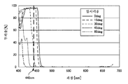
반사막(31)을 예를 들어 도 3에 도시하는 다이크로익 미러로 구성한 경우에는, 각 유전체층의 적층수, 각 유전체층의 두께, 각 유전체층의 형성 재료 등을 조정함으로써, 반사막(31)에 입사하는 광의 투과율(반사율)의 입사각 의존성을 설정하기 쉬워진다. 도 4에, 본 실시 형태에서 사용하는 반사막(31)의 광투과율의 입사각 의존성의 일례를 나타낸다. 도 4에 나타내는 특성의 횡축은 입사광의 파장 이고, 종축은 투과율이다.In the case where the
도 4에 도시하는 예에서는, 반사막(31)은, 적색광 및 녹색광을 포함하는 파장 대역(약 480 내지 680㎚에 걸치는 파장 영역)의 광을, 그 입사각(θ)에 관계없이 선택적으로 반사하도록 설계되어 있다. 그로 인해, 적색광 및 녹색광을 포함하는 파장 대역의 광(형광체층(32)으로부터의 발광광)에 대해서는, 그 광의 입사각(θ)에 관계없이, 투과율이 대략 0이 된다. 즉, 적색광 및 녹색광을 포함하는 파장 영역의 광은, 입사각(θ)에 관계없이, 반사막(31)에서 모두 반사된다.In the example shown in FIG. 4, the reflecting
한편, 파장 445㎚의 청색광(여기광(L))에 대해서는, 그 입사각(θ)이 약 20도 이하일 때에 청색광이 투과하고, 입사각(θ)이 약 20도보다 큰 경우에는 청색광이 반사되도록, 반사막(31)이 설계되어 있다. 그로 인해, 도 4에 도시한 바와 같이, 청색광(여기광(L))의 파장 445㎚(두꺼운 파선)에서는, 광의 입사각(θ)이 0도(실선) 및 15도(파선)일 때는, 투과율이 커진다. 또한, 청색광의 입사각(θ)이 30도(일점 쇄선), 45도(점선) 및 60도(2점 쇄선)일 때는, 파장 445㎚에 있어서의 투과율이 작아진다. 즉, 형광체층(32) 내에서 산란 및 반사된 여기광(L) 중, 약 20도보다 큰 입사각(θ)으로 반사막(31)에 입사하는 여기광 성분은, 반사막(31)에서 제2 집광 광학계(15)를 향하는 방향으로 반사된다.On the other hand, with respect to the blue light (excitation light L) having a wavelength of 445 nm, blue light transmits when the incident angle θ is about 20 degrees or less, and blue light is reflected when the incident angle θ is larger than about 20 degrees. The
또한, 상술한 바와 같이, 반사막(31)의 투과율의 입사각 의존성에 따라서 제1 집광 광학계(12)의 구성이 설계된다. 예를 들어, 반사막(31)이, 도 4에 도시하는 투과율의 입사각 의존성을 갖는 경우에는, 여기광(L)의 이용 효율을 저하시키지 않기 위하여, 집광된 여기광(L)의 입사각(θ)이, 약 20도 이하로 되도록, 제1 집광 광학계(12)가 설계된다.In addition, as described above, the configuration of the first condensing
형광체층(32)은, 여기광(L)의 입사에 의해, 소정 파장 대역의 광을 발광하는 층상의 형광체이다. 본 실시 형태에서는, 여기광(L)의 투과광과 형광체층(32)에서의 발광광을 합파하여 백색광 LW를 생성하므로, 형광체층(32)으로서는, 예를 들어 YAG(Yttrium Aluminum Garnet)계 형광 재료 등으로 형성한다. 이 경우, 청색의 여기광(L)이 입사되면, 형광체층(32)으로부터는 파장 480 내지 680㎚의 대역의 광(황색광)이 발광된다. 또한, 형광체층(32)으로서는, 적색광 및 녹색광을 포함하는 파장 대역의 광을 발광하는 막이면, 임의의 재료로 구성할 수 있지만, 발광 효율 및 내열성의 관점에서는 YAG계 형광체 재료를 사용하는 것이 바람직하다.The
또한, 형광체층(32)은, 형광 재료와 바인더를 혼합한 소정의 형광제를 반사막(31) 상에 도포함으로써 형성된다. 도 2의 (a) 내지 (c)에 나타내는 예에서는 형광체층(32)을 반사막(31)의 전체면에 걸쳐서 형성하므로, 형광체층(32)의 표면 형상도 도넛 형상으로 된다. 또한, 형광체층(32)은, 여기광(L)이 입사되는 영역에 형성되어 있으면 되므로, 형광체층(32)의 형상은, 도 2의 (a) 내지 (c)에 나타내는 예에 한정되지 않고, 예를 들어, 형광체층(32)의 반경 방향의 폭이 반사막(31)의 폭보다 좁아도 된다.In addition, the
또한, 형광체층(32)에서의 발광량 및 여기광(L)의 투과량은, 예를 들어 형광체층(32)의 두께나 형광체 밀도(함유량) 등에 의해 조정할 수 있다. 그로 인해, 본 실시 형태에서는, 광원 장치부(1)로부터의 출사광이 백색광이 되도록, 형광체층(32)의 두께나 형광체 밀도 등을 조정한다.The amount of light emitted from the
반사 방지막(33)은, 투명 기판(30)의 여기광(L)의 입사측 표면에 형성되고, 여기광(L)의 집광광을 형광 부재(13)에 입사하였 때에, 그 입사면에서 발생하는 여기광(L)의 반사를 방지한다. 이에 의해, 여기광(L)의 이용 효율을 향상시킬 수 있다.The
또한, 상기 실시 형태에서는, 형광 부재(13)에, 반사막(31) 및 반사 방지막(33)을 형성하는 예를 설명하였지만, 본 발명은 이에 한정되지 않는다. 예를 들어, 광원 장치부(1)로부터의 출사광의 출력이 작아도 문제가 없는 용도 등에 본 실시 형태의 광원 장치부(1)를 적용하는 경우에는, 반사막(31) 및 반사 방지막(33) 중 어느 한쪽 또는 양쪽을 구비하지 않는 구성으로 해도 된다. 또한, 상기 실시 형태의 형광 부재(13)에서는, 투명 기판(30) 상에 반사막(31)을 통하여 층상의 형광체(형광체층(32))를 설치하는 예를 설명하였지만, 본 발명은 이에 한정되지 않는다. 예를 들어, 형광체를 충분한 강성을 갖는 판 형상 부재로 구성한 경우에는, 투명 기판(30)을 설치하지 않아도 된다.In addition, in the said embodiment, although the example which forms the
[4. 광원 장치부의 동작예][4. Operation example of light source device section]
도 5에, 본 실시 형태의 광원 장치부(1)의 동작의 모습을 나타낸다. 본 실시 형태의 광원 장치부(1)에서는, 우선, 여기광원(11)으로부터 사출된 여기광(L)(이 예에서는 청색광)을, 제1 집광 광학계(12)로 집광한다. 그리고, 그 집광광(집광된 여기광(L))은, 형광 부재(13)의 반사 방지막(33)측으로부터 소정의 입사각(θ)으로 형광 부재(13)에 입사된다. 또한, 본 실시 형태에서는, 모터(14)에 의해, 형광 부재(13)를 소정의 회전수로 회전시킨 상태에서, 집광광을 형광 부재(13)에 조사한다.5, the operation | movement state of the light
형광 부재(13)에 입사된 집광광은, 반사 방지막(33), 투명 기판(30) 및 반사막(31)을 통과하여 형광체층(32)에 입사된다. 또한, 상술한 바와 같이, 반사막(31)은, 소정의 입사각(θ) 이하의 여기광(L)을 투과하도록 설계되어 있으므로, 형광 부재(13)에 입사된 집광광은 반사막(31)에서 반사되지 않는다.The condensed light incident on the
그리고, 집광광(여기광(L))이 형광체층(32)에 입사되면, 그 일부는, 형광체층(32)을 통과하지만, 나머지는, 주로, 형광체층(32)에서 흡수된다. 이 흡수된 여기광(L)에 의해 형광체층(32)이 여기되고, 형광체층(32)으로부터 소정 파장 대역의 광(이 예에서는 적색광 및 녹색광을 포함하는 황색광)이 발광한다. 이 결과, 여기광(L)의 투과 성분과, 형광체층(32)으로부터의 발광광이 합파되어, 형광체층(32)으로부터 백색광이 사출된다.And when condensed light (excitation light L) enters the
또한, 이때, 형광체층(32)의 발광광은, 제2 집광 광학계(15)을 향하는 방향뿐만 아니라, 투명 기판(30)을 향하는 방향으로도 사출된다. 또한, 형광체층(32)에 입사된 여기광(L)의 일부는, 형광체층(32) 내에서 투명 기판(30)을 향하는 방향으로도 산란 및 반사된다. 그러나, 본 실시 형태의 형광 부재(13)에서는, 상술한 바와 같이, 투명 기판(30)과 형광체층(32) 사이에 반사막(31)을 형성하고 있으므로, 투명 기판(30)을 향하는 방향으로 사출된 발광광 및 여기광 성분은, 반사막(31)에 의해 제2 집광 광학계(15)를 향하는 방향으로 반사된다. 이때, 반사막(31)에서 반사된 여기광 성분은, 형광체층(32)에서 흡수되어, 다시 형광체층(32)을 발광시킨다. 그로 인해, 본 실시 형태와 같이, 투명 기판(30)과 형광체층(32) 사이에 반사막(31)을 형성한 경우에는, 여기광(L)의 이용 효율을 향상시킬 수 있어, 발광광의 광량을 더욱 증대시킬 수 있다.In this case, the emitted light of the
또한, 실제로, 본 발명자는, 광원 장치부(1)의 각 부의 파라미터를 다음과 같이 설정하여, 광원 장치부(1)로부터의 출사광의 스펙트럼 특성을 조사하였다.In addition, the present inventors set the parameter of each part of the light
여기광원(11)(청색 레이저)의 파장: 445㎚Wavelength of excitation light source 11 (blue laser): 445 nm
여기광(L)의 집광 직경: 1㎜Condensing diameter of excitation light L: 1 mm
여기광(L)의 입사각(θ): 20도 이하Incident angle (theta) of excitation light L: 20 degrees or less
형광 부재(13)의 회전수: 3000rpmThe rotation speed of the fluorescent member 13: 3000 rpm
제2 집광 광학계(15) 및 형광체층(32) 사이의 거리: 1㎜ 이하Distance between the second condensing
투명 기판(30)의 형성 재료: 유리Forming Material of Transparent Substrate 30: Glass
투명 기판(30)의 직경: 30㎜Diameter of the transparent substrate 30: 30 mm
반사막(31)의 투과 특성: 도 4에 나타내는 특성Transmission characteristics of the reflective film 31: characteristics shown in FIG.
형광체층(32)의 형성 재료: YAG계 형광체Formation Material of Phosphor Layer 32: YAG-Based Phosphor
형광체층(32)의 두께: 50㎛Thickness of phosphor layer 32: 50 μm
형광체층(32)의 폭: 5㎜Width of phosphor layer 32: 5 mm
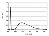
도 6에, 상기 조건에서 얻어진 광원 장치부(1)로부터의 출사광의 스펙트럼 특성을 나타낸다. 또한, 도 6에 나타내는 특성에서는, 횡축이 파장이고, 종축이 출사광의 강도(임의 단위)이다. 도 6으로부터 명백해진 바와 같이, 상기 조건에서는, 출사광에, 파장 445㎚ 부근의 광 성분(청색광 성분)과, 약 480 내지 680㎚에 걸친 파장 영역의 광 성분, 즉, 적색광 성분 및 녹색광 성분을 포함하는 광 성분이 포함되어 있는 것을 알 수 있다. 이것으로부터도, 본 실시 형태의 광원 장치부(1)로부터, 백색광 LW가 출사되고 있는 것을 알 수 있다.6 shows the spectral characteristics of the emitted light from the light
상술한 바와 같이, 본 실시 형태에서는, 고체 발광 소자를 사용하여 백색광을 광원 장치부(1)로부터 사출할 수 있다. 그로 인해, 본 실시 형태는, 예를 들어 3LCD 방식의 프로젝터 등과 같이, 백색광을 사출하는 광원 장치를 필요로 하는 용도에도 적용 가능하다. 즉, 본 실시 형태에서는, 여러 가지 용도에 적용 가능한 무수은의 광원 장치부(1)(조명 장치) 및 그것을 구비하는 화상 표시 장치(10)를 제공할 수 있다.As described above, in the present embodiment, the white light can be emitted from the light
본 실시 형태의 광원 장치부(1)는, 수은 램프를 사용할 필요가 없으므로, 최근의 환경 문제에 대응할 수 있다. 또한, 본 실시 형태에서는, 수은 램프에 비하여 보다 수명이 길고 또한 휘도 저하도 작은 광원 장치부(1) 및 화상 표시 장치(10)를 제공할 수 있다. 또한, 본 실시 형태와 같이, 여기광원(11)에 고체 발광 소자를 사용한 경우에는, 수은 램프에 비하여 점등 시간을 더욱 단축할 수 있다.Since the light
또한, 본 실시 형태의 광원 장치부(1)와 같이 여기광원(11)으로서 반도체 레이저를 사용한 경우에는, 예를 들어 LED(Light Emitting Diode) 등의 고체 광원에 비해서도, 충분히 고휘도의 광을 사출할 수 있어, 고휘도 광원의 실현이 가능해진다. 또한, 본 실시 형태와 같이, 청색광 레이저로 형광체층(32)을 발광시켜 백색광 LW를 생성하는 구성은, 적색광, 녹색광 및 청색광의 각 고체 광원을 개별로 준비하여 백색광을 생성하는 구성에 비하여 더욱 저렴하다.In addition, when a semiconductor laser is used as the
상기 실시 형태에서는, 광원 장치부(1)(조명 장치)를 3LCD 방식의 프로젝터에 적용하는 예를 설명하였지만, 본 발명은 이에 한정되지 않고, 백색광을 필요로 하는 임의의 화상 표시 장치에 적용 가능하며, 마찬가지의 효과를 얻을 수 있다.In the above embodiment, an example in which the light source device unit 1 (lighting device) is applied to a 3LCD type projector has been described, but the present invention is not limited thereto, and can be applied to any image display device that requires white light. The same effect can be obtained.
또한, 상기 실시 형태에서는, 광원 장치부(1)(조명 장치)의 출사광을 백색광으로 하는 예를 설명하였지만, 본 발명은 이에 한정되지 않는다. 예를 들어, 출사광으로서 시안 광(또는 마젠타광)을 필요로 하는 용도에서는, 여기광(L)으로서 청색광을 사용하고, 형광체층(32)을 녹색광(또는 적색광)만을 발광하는 형광 재료로 형성하면 된다. 즉, 필요로 하는 출사광의 파장(색)에 따라서, 여기광(L)의 파장과 형광체층(32)의 형성 재료의 조합을 적절히 선택하면 된다.In addition, in the said embodiment, although the example which made the output light of the light source device part 1 (lighting device) into white light was demonstrated, this invention is not limited to this. For example, in applications requiring cyan light (or magenta light) as the outgoing light, blue light is used as the excitation light L, and the
1: 광원 장치부(조명 장치)
2: 광학 엔진부(화상 투영부)
10: 화상 표시 장치
11: 여기광원
12: 제1 집광 광학계
13: 형광 부재
14: 모터
15: 제2 집광 광학계
20: 분광 광학계
21: 제1 LCD 패널
22: 제2 LCD 패널
23: 제3 LCD 패널
24: 프리즘
25: 투영 광학계
30: 투명 기판
31: 반사막
32: 형광체층(형광체)
33: 반사 방지막 1: light source unit (lighting unit)
2: optical engine unit (image projection unit)
10: image display device
11: excitation light source
12: first condensing optical system
13: fluorescent member
14: motor
15: second condensing optical system
20: spectrophotometer
21: first LCD panel
22: second LCD panel
23: third LCD panel
24: Prism
25: projection optical system
30: transparent substrate
31: reflecting film
32: phosphor layer (phosphor)
33: antireflection film
Claims (9)
상기 여기광이 조사되었을 때에, 상기 제1 파장보다 긴 제2 파장을 갖는 광을 발광함과 함께, 상기 여기광의 일부를 투과시켜, 상기 투과한 상기 제1 파장의 여기광과 상기 발광한 제2 파장의 광을 합파하여 사출하는 형광체와,
상기 형광체의 상기 여기광의 조사 위치를 시간 경과에 따라 이동시키는 구동부를 구비하는, 조명 장치.An excitation light source for emitting excitation light having a first wavelength,
When the excitation light is irradiated, the light having a second wavelength longer than the first wavelength is emitted, and a part of the excitation light is transmitted to transmit the excitation light of the first wavelength and the second light emission. A phosphor that combines and emits light of a wavelength;
And a driving unit which moves the irradiation position of the excitation light of the phosphor over time.
상기 광원 장치부로부터 사출된 광을 사용하여 소정의 화상광을 생성하고, 상기 생성된 화상광을 외부에 투영하는 화상 투영부를 구비하는, 화상 표시 장치.An excitation light source that emits an excitation light having a first wavelength and a light having a second wavelength longer than the first wavelength when the excitation light is irradiated, and transmits a part of the excitation light to transmit A light source device unit including a phosphor that combines and emits the excitation light of the first wavelength and the light of the emitted second wavelength, and a driving unit that moves the irradiation position of the excitation light of the phosphor over time;
And an image projector for generating predetermined image light by using the light emitted from the light source device and projecting the generated image light to the outside.
Applications Claiming Priority (2)
| Application Number | Priority Date | Filing Date | Title |
|---|---|---|---|
| JP2010137192A JP5767444B2 (en) | 2010-06-16 | 2010-06-16 | Light source device and image projection device |
| JPJP-P-2010-137192 | 2010-06-16 |
Related Child Applications (1)
| Application Number | Title | Priority Date | Filing Date |
|---|---|---|---|
| KR1020170059777A Division KR101973262B1 (en) | 2010-06-16 | 2017-05-15 | Light source device and image display apparatus |
Publications (1)
| Publication Number | Publication Date |
|---|---|
| KR20110137245A true KR20110137245A (en) | 2011-12-22 |
Family
ID=45328370
Family Applications (2)
| Application Number | Title | Priority Date | Filing Date |
|---|---|---|---|
| KR1020110054984A KR20110137245A (en) | 2010-06-16 | 2011-06-08 | Illumination device and image display apparatus |
| KR1020170059777A KR101973262B1 (en) | 2010-06-16 | 2017-05-15 | Light source device and image display apparatus |
Family Applications After (1)
| Application Number | Title | Priority Date | Filing Date |
|---|---|---|---|
| KR1020170059777A KR101973262B1 (en) | 2010-06-16 | 2017-05-15 | Light source device and image display apparatus |
Country Status (5)
| Country | Link |
|---|---|
| US (6) | US9052582B2 (en) |
| JP (1) | JP5767444B2 (en) |
| KR (2) | KR20110137245A (en) |
| CN (1) | CN102289140B (en) |
| TW (1) | TWI421448B (en) |
Cited By (1)
| Publication number | Priority date | Publication date | Assignee | Title |
|---|---|---|---|---|
| WO2019231080A1 (en) * | 2018-05-30 | 2019-12-05 | 액츠 주식회사 | Light source device and image projection device comprising same |
Families Citing this family (63)
| Publication number | Priority date | Publication date | Assignee | Title |
|---|---|---|---|---|
| JP5767444B2 (en) | 2010-06-16 | 2015-08-19 | ソニー株式会社 | Light source device and image projection device |
| US10688527B2 (en) | 2011-09-22 | 2020-06-23 | Delta Electronics, Inc. | Phosphor device comprising plural phosphor agents for converting waveband light into plural color lights with different wavelength peaks |
| TWI448806B (en) | 2011-09-22 | 2014-08-11 | Delta Electronics Inc | Phosphor device and illumination system and projection equipment with the same |
| US10310363B2 (en) | 2011-09-22 | 2019-06-04 | Delta Electronics, Inc. | Phosphor device with spectrum of converted light comprising at least a color light |
| WO2013046243A1 (en) * | 2011-09-26 | 2013-04-04 | 日立コンシューマエレクトロニクス株式会社 | Light source apparatus |
| TWI437350B (en) * | 2011-12-27 | 2014-05-11 | Delta Electronics Inc | Illumination system and wavelength-transforming device thereof |
| CN102723422B (en) * | 2011-12-31 | 2015-04-29 | 深圳市光峰光电技术有限公司 | Wavelength conversion apparatus and luminous apparatus |
| CN102854723B (en) * | 2012-01-07 | 2015-02-04 | 深圳市光峰光电技术有限公司 | Light-emitting device and projection apparatus |
| JP2013162021A (en) * | 2012-02-07 | 2013-08-19 | Seiko Epson Corp | Wavelength conversion element, light source device, and projector |
| JP2013162020A (en) | 2012-02-07 | 2013-08-19 | Seiko Epson Corp | Wavelength conversion element, light source device, and projector |
| CN103376634B (en) | 2012-04-24 | 2015-11-18 | 中强光电股份有限公司 | Light source module and projection arrangement |
| JP5962904B2 (en) | 2012-04-26 | 2016-08-03 | パナソニックIpマネジメント株式会社 | Light source device and projection display device including the light source device |
| JP6086193B2 (en) | 2012-09-20 | 2017-03-01 | カシオ計算機株式会社 | Light source device, lighting method of light source device, and projector |
| JP6270012B2 (en) * | 2012-09-20 | 2018-01-31 | カシオ計算機株式会社 | Light source device, lighting method of light source device, and projector |
| JP2014203852A (en) * | 2013-04-01 | 2014-10-27 | 日本電気硝子株式会社 | Wavelength conversion member and light emitting device |
| WO2014174559A1 (en) * | 2013-04-22 | 2014-10-30 | 日立マクセル株式会社 | Light source apparatus and image display apparatus |
| JP2014235250A (en) * | 2013-05-31 | 2014-12-15 | ソニー株式会社 | Light source device and projector |
| JP2015034866A (en) * | 2013-08-08 | 2015-02-19 | 日本電気硝子株式会社 | Projector fluorescent wheel and projector light-emitting device |
| JP2015034867A (en) * | 2013-08-08 | 2015-02-19 | 日本電気硝子株式会社 | Projector fluorescent wheel and projector light-emitting device |
| TWI509344B (en) | 2013-09-18 | 2015-11-21 | Coretronic Corp | Illumination system and projection apparatus |
| TWI524129B (en) | 2013-11-21 | 2016-03-01 | 中強光電股份有限公司 | Illumination system and projection apparatus |
| TW201528379A (en) * | 2013-12-20 | 2015-07-16 | Applied Materials Inc | Dual wavelength annealing method and apparatus |
| CN104765237B (en) * | 2014-01-03 | 2016-08-17 | 台达电子工业股份有限公司 | Optical projection apparatus |
| US20160313633A1 (en) * | 2014-01-08 | 2016-10-27 | Nec Display Solutions, Ltd. | Light source device and projection-type display device |
| JP2015163947A (en) | 2014-02-03 | 2015-09-10 | キヤノン株式会社 | Light source optical system, light source device having the same, and image display device |
| JP2015155958A (en) * | 2014-02-20 | 2015-08-27 | セイコーエプソン株式会社 | Illumination device and projector |
| JP2015166787A (en) * | 2014-03-04 | 2015-09-24 | カシオ計算機株式会社 | Light source device and projection device |
| JP6225812B2 (en) | 2014-04-18 | 2017-11-08 | 日亜化学工業株式会社 | Light emitting device |
| JP6458390B2 (en) * | 2014-07-31 | 2019-01-30 | 日亜化学工業株式会社 | Light source device and projector provided with the light source device |
| CN104174992B (en) * | 2014-08-26 | 2016-04-13 | 济南金威刻科技发展有限公司 | Mixing cutting machine generating device of laser |
| JP6507548B2 (en) * | 2014-09-26 | 2019-05-08 | セイコーエプソン株式会社 | Wavelength conversion element, light source device, projector |
| CN105629486B (en) * | 2014-10-28 | 2019-03-29 | 深圳光峰科技股份有限公司 | 3D projection display system |
| US10067413B2 (en) * | 2014-10-28 | 2018-09-04 | Sony Corporation | Light source device and projector |
| JP6489831B2 (en) * | 2015-01-07 | 2019-03-27 | スタンレー電気株式会社 | Wavelength converter, method for manufacturing the same, and illumination device using the wavelength converter |
| WO2016116975A1 (en) * | 2015-01-20 | 2016-07-28 | ソニー株式会社 | Light source device, image display device, and light source module |
| CN105988274A (en) * | 2015-03-20 | 2016-10-05 | 台达电子工业股份有限公司 | Optical device |
| WO2016181858A1 (en) * | 2015-05-08 | 2016-11-17 | コニカミノルタ株式会社 | Light source device and projection device |
| JP6536212B2 (en) * | 2015-06-23 | 2019-07-03 | セイコーエプソン株式会社 | Wavelength conversion element, light source device and projector |
| CN106896632A (en) * | 2015-12-03 | 2017-06-27 | 精工爱普生株式会社 | Fluorophor, Wavelength changing element, light supply apparatus and projecting apparatus |
| JP2017123317A (en) * | 2016-01-08 | 2017-07-13 | パナソニックIpマネジメント株式会社 | Luminaire |
| CN107193177B (en) * | 2016-03-14 | 2020-11-17 | 深圳光峰科技股份有限公司 | Light source system and projection device thereof |
| CN105915871A (en) * | 2016-05-09 | 2016-08-31 | 南京熊猫电子股份有限公司 | Laser TV full-color generation method and device in 3 LCD mode |
| CN109154768B (en) | 2016-05-20 | 2021-05-28 | 索尼公司 | Light source apparatus and projection display apparatus |
| WO2017203782A1 (en) | 2016-05-24 | 2017-11-30 | ソニー株式会社 | Light source device and projection display device |
| DE112017002755T5 (en) | 2016-06-01 | 2019-02-21 | Canon Kabushiki Kaisha | WAVE LENGTH CONVERSION ELEMENT, LIGHT SOURCE DEVICE AND IMAGE PROJECTION DEVICE |
| JP2016194709A (en) * | 2016-06-23 | 2016-11-17 | セイコーエプソン株式会社 | Light source device and projector |
| JP2018028647A (en) * | 2016-08-20 | 2018-02-22 | セイコーエプソン株式会社 | Wavelength conversion element, light source device, and projector |
| US10884328B2 (en) * | 2016-08-30 | 2021-01-05 | Sony Corporation | Projection display apparatus |
| EP3571398A1 (en) * | 2017-02-22 | 2019-11-27 | Siemens Gamesa Renewable Energy A/S | A tower for a wind turbine and a wind turbine |
| JP6916073B2 (en) * | 2017-02-28 | 2021-08-11 | パナソニック株式会社 | Optical device |
| JP6926589B2 (en) * | 2017-03-29 | 2021-08-25 | セイコーエプソン株式会社 | Light source device and projector |
| CN109917610B (en) | 2017-12-12 | 2020-12-01 | 中强光电股份有限公司 | Light source module and projection device |
| WO2019142698A1 (en) * | 2018-01-19 | 2019-07-25 | ソニー株式会社 | Light source device and projection-type display device |
| JP7198978B2 (en) * | 2018-04-27 | 2023-01-05 | パナソニックIpマネジメント株式会社 | Phosphor wheel, light source device and projection display device |
| CN110505461B (en) * | 2018-05-18 | 2022-07-29 | 深圳Tcl新技术有限公司 | Laser projection television |
| JP7163408B2 (en) * | 2018-11-26 | 2022-10-31 | 京セラ株式会社 | Light source device and lighting device |
| CN110213471B (en) * | 2019-06-28 | 2021-01-08 | 维沃移动通信(杭州)有限公司 | Terminal device |
| JP7071702B2 (en) * | 2019-07-22 | 2022-05-19 | カシオ計算機株式会社 | Light source device and projection device |
| JP7283327B2 (en) * | 2019-09-20 | 2023-05-30 | セイコーエプソン株式会社 | Wavelength conversion element, light source device and projector |
| JP7294089B2 (en) * | 2019-11-28 | 2023-06-20 | セイコーエプソン株式会社 | Light source device and projector |
| CN114613253B (en) * | 2020-12-09 | 2024-01-23 | 极米科技股份有限公司 | Optical system and display device |
| JP2022112948A (en) | 2021-01-22 | 2022-08-03 | セイコーエプソン株式会社 | Light source device and projector |
| JP2022149550A (en) * | 2021-03-25 | 2022-10-07 | セイコーエプソン株式会社 | Wavelength converter, light source device, projector, and method for manufacturing wavelength converter |
Family Cites Families (44)
| Publication number | Priority date | Publication date | Assignee | Title |
|---|---|---|---|---|
| JPH06265894A (en) | 1993-03-11 | 1994-09-22 | Teruki Fujiyama | Color display device |
| AU7799494A (en) | 1993-09-17 | 1995-04-03 | Proxima Corporation | Compact projection illumination system and method of using same |
| JP4182804B2 (en) | 2003-04-28 | 2008-11-19 | セイコーエプソン株式会社 | Illumination device and projection display device |
| JP4829470B2 (en) * | 2003-05-14 | 2011-12-07 | Necディスプレイソリューションズ株式会社 | Projection display |
| CN1624570A (en) * | 2003-12-03 | 2005-06-08 | 精工爱普生株式会社 | Projector |
| US7431463B2 (en) * | 2004-03-30 | 2008-10-07 | Goldeneye, Inc. | Light emitting diode projection display systems |
| TWI398188B (en) * | 2004-08-31 | 2013-06-01 | Showa Denko Kk | A luminous body, and a lighting and display device using the luminous body |
| TWI254821B (en) * | 2004-10-01 | 2006-05-11 | Delta Electronics Inc | Backlight module |
| JP2006119440A (en) * | 2004-10-22 | 2006-05-11 | Olympus Corp | Surface sequential illuminating apparatus and image projecting apparatus |
| US7391569B2 (en) * | 2004-12-29 | 2008-06-24 | 3M Innovative Properties Company | Projection system including intrinsic polarizer |
| WO2006098450A1 (en) * | 2005-03-18 | 2006-09-21 | Mitsubishi Chemical Corporation | Light-emitting device, white light-emitting device, illuminator, and image display |
| FR2883645A1 (en) | 2005-03-22 | 2006-09-29 | Thomson Licensing Sa | IMAGING SYSTEM FOR PROJECTOR AND CORRESPONDING PROJECTOR |
| US7445340B2 (en) * | 2005-05-19 | 2008-11-04 | 3M Innovative Properties Company | Polarized, LED-based illumination source |
| WO2006133214A2 (en) | 2005-06-07 | 2006-12-14 | Optical Research Associates | Phosphor wheel illuminator |
| JP4910315B2 (en) * | 2005-06-20 | 2012-04-04 | セイコーエプソン株式会社 | Display device and light emitting device |
| US7543959B2 (en) * | 2005-10-11 | 2009-06-09 | Philips Lumiled Lighting Company, Llc | Illumination system with optical concentrator and wavelength converting element |
| JP2007109947A (en) * | 2005-10-14 | 2007-04-26 | Toyoda Gosei Co Ltd | Phosphor plate and light-emitting device provided with the same |
| US7369320B2 (en) * | 2005-12-30 | 2008-05-06 | 3M Innovative Properties Company | Projection system with beam homogenizer |
| US20070187580A1 (en) | 2006-02-14 | 2007-08-16 | Microvision, Inc. | Photoluminescent light sources, and scanned beam systems and methods of using same |
| US7682850B2 (en) * | 2006-03-17 | 2010-03-23 | Philips Lumileds Lighting Company, Llc | White LED for backlight with phosphor plates |
| US7889430B2 (en) * | 2006-05-09 | 2011-02-15 | Ostendo Technologies, Inc. | LED-based high efficiency illumination systems for use in projection systems |
| JP2008052070A (en) | 2006-08-25 | 2008-03-06 | Samsung Electronics Co Ltd | Color wheel, visible light source, and projection image display device and method |
| US7547114B2 (en) * | 2007-07-30 | 2009-06-16 | Ylx Corp. | Multicolor illumination device using moving plate with wavelength conversion materials |
| JP2009042569A (en) * | 2007-08-09 | 2009-02-26 | Panasonic Corp | Projection type display |
| US20090051884A1 (en) * | 2007-08-21 | 2009-02-26 | United Microelectronics Corp. | Projection apparatus |
| CN101498401B (en) * | 2008-01-29 | 2011-08-03 | 绎立锐光科技开发(深圳)有限公司 | Light source structure for improving light conversion efficiency by fluorescent powder |
| US8471283B2 (en) * | 2008-02-25 | 2013-06-25 | Kabushiki Kaisha Toshiba | White LED lamp, backlight, light emitting device, display device and illumination device |
| JP2009245712A (en) * | 2008-03-31 | 2009-10-22 | Stanley Electric Co Ltd | Illumination fixture |
| US8764198B2 (en) * | 2008-04-29 | 2014-07-01 | Himax Display, Inc. | Projection system having rotationally asymmetrical illumination unit for emitting light along optic axis |
| JP4662185B2 (en) | 2008-05-15 | 2011-03-30 | カシオ計算機株式会社 | Light source device and projector |
| JP5152586B2 (en) * | 2008-09-30 | 2013-02-27 | カシオ計算機株式会社 | Light source device and projector |
| JP5527571B2 (en) * | 2008-09-30 | 2014-06-18 | カシオ計算機株式会社 | Light emitting device, light source device, and projector using the light source device |
| JP5431706B2 (en) * | 2008-10-01 | 2014-03-05 | ミネベア株式会社 | Light emitting device |
| CN201417358Y (en) * | 2009-02-20 | 2010-03-03 | 红蝶科技(深圳)有限公司 | Miniature projection optical engine with high lighting effect |
| CN101825836A (en) * | 2009-03-02 | 2010-09-08 | 鸿富锦精密工业(深圳)有限公司 | Light source system |
| JP4678556B2 (en) * | 2009-03-17 | 2011-04-27 | カシオ計算機株式会社 | Light emitting device, light source device, and projector using the light source device |
| JP4756403B2 (en) * | 2009-06-30 | 2011-08-24 | カシオ計算機株式会社 | Light source device and projector |
| JP4711154B2 (en) * | 2009-06-30 | 2011-06-29 | カシオ計算機株式会社 | Light source device and projector |
| US8684560B2 (en) * | 2009-11-18 | 2014-04-01 | Stanley Electric Co., Ltd. | Semiconductor light source apparatus and lighting unit |
| US8556437B2 (en) | 2009-12-17 | 2013-10-15 | Stanley Electric Co., Ltd. | Semiconductor light source apparatus and lighting unit |
| JP5567844B2 (en) * | 2010-01-29 | 2014-08-06 | 日立コンシューマエレクトロニクス株式会社 | Projection display device |
| JP5617288B2 (en) * | 2010-03-18 | 2014-11-05 | セイコーエプソン株式会社 | Lighting device and projector |
| JP5767444B2 (en) * | 2010-06-16 | 2015-08-19 | ソニー株式会社 | Light source device and image projection device |
| JP5770433B2 (en) * | 2010-06-18 | 2015-08-26 | ソニー株式会社 | Light source device and image projection device |
-
2010
- 2010-06-16 JP JP2010137192A patent/JP5767444B2/en active Active
-
2011
- 2011-06-02 TW TW100119372A patent/TWI421448B/en active
- 2011-06-08 KR KR1020110054984A patent/KR20110137245A/en active Search and Examination
- 2011-06-09 US US13/156,744 patent/US9052582B2/en active Active
- 2011-06-09 CN CN201110152826.6A patent/CN102289140B/en active Active
-
2015
- 2015-04-24 US US14/695,396 patent/US9369682B2/en active Active
-
2016
- 2016-03-21 US US15/075,428 patent/US9618738B2/en active Active
- 2016-12-15 US US15/380,435 patent/US9733558B2/en active Active
-
2017
- 2017-04-10 US US15/482,969 patent/US9995927B2/en active Active
- 2017-05-15 KR KR1020170059777A patent/KR101973262B1/en active IP Right Grant
-
2018
- 2018-04-24 US US15/960,892 patent/US10429636B2/en active Active
Cited By (1)
| Publication number | Priority date | Publication date | Assignee | Title |
|---|---|---|---|---|
| WO2019231080A1 (en) * | 2018-05-30 | 2019-12-05 | 액츠 주식회사 | Light source device and image projection device comprising same |
Also Published As
| Publication number | Publication date |
|---|---|
| TWI421448B (en) | 2014-01-01 |
| TW201235618A (en) | 2012-09-01 |
| US9995927B2 (en) | 2018-06-12 |
| US10429636B2 (en) | 2019-10-01 |
| JP2012003923A (en) | 2012-01-05 |
| KR20170056494A (en) | 2017-05-23 |
| US20110310362A1 (en) | 2011-12-22 |
| US20150229891A1 (en) | 2015-08-13 |
| CN102289140A (en) | 2011-12-21 |
| US20170097561A1 (en) | 2017-04-06 |
| US20180239126A1 (en) | 2018-08-23 |
| US20160202468A1 (en) | 2016-07-14 |
| CN102289140B (en) | 2016-08-03 |
| JP5767444B2 (en) | 2015-08-19 |
| US9618738B2 (en) | 2017-04-11 |
| US9369682B2 (en) | 2016-06-14 |
| US9052582B2 (en) | 2015-06-09 |
| KR101973262B1 (en) | 2019-08-16 |
| US9733558B2 (en) | 2017-08-15 |
| US20170212414A1 (en) | 2017-07-27 |
Similar Documents
| Publication | Publication Date | Title |
|---|---|---|
| KR101973262B1 (en) | Light source device and image display apparatus | |
| US10852630B2 (en) | Illumination device and image display apparatus | |
| WO2015111145A1 (en) | Light source device and image display device using same | |
| JP6137238B2 (en) | Light source device and image projection device | |
| JP6819759B2 (en) | Light source device and image projection device | |
| JP6388051B2 (en) | Light source device and image projection device | |
| JP6353583B2 (en) | Light source device and image projection device | |
| JP6149991B2 (en) | Light source device and image projection device | |
| JP6680340B2 (en) | Light source device and image projection device | |
| JP6453495B2 (en) | Light source device and image projection device | |
| JP6279516B2 (en) | Light source device and image projection device | |
| JP2018151667A (en) | Light source device and image projection device |
Legal Events
| Date | Code | Title | Description |
|---|---|---|---|
| A201 | Request for examination | ||
| AMND | Amendment | ||
| E902 | Notification of reason for refusal | ||
| AMND | Amendment | ||
| E601 | Decision to refuse application | ||
| AMND | Amendment | ||
| J301 | Trial decision |
Free format text: TRIAL NUMBER: 2017101003198; TRIAL DECISION FOR APPEAL AGAINST DECISION TO DECLINE REFUSAL REQUESTED 20170630 Effective date: 20170828 |