KR20110097641A - Imprint apparatus, template of imprint apparatus, and article manufacturing method - Google Patents
Imprint apparatus, template of imprint apparatus, and article manufacturing method Download PDFInfo
- Publication number
- KR20110097641A KR20110097641A KR1020110013709A KR20110013709A KR20110097641A KR 20110097641 A KR20110097641 A KR 20110097641A KR 1020110013709 A KR1020110013709 A KR 1020110013709A KR 20110013709 A KR20110013709 A KR 20110013709A KR 20110097641 A KR20110097641 A KR 20110097641A
- Authority
- KR
- South Korea
- Prior art keywords
- region
- resin
- pattern
- template
- uncured resin
- Prior art date
Links
Images


Classifications
-
- B—PERFORMING OPERATIONS; TRANSPORTING
- B29—WORKING OF PLASTICS; WORKING OF SUBSTANCES IN A PLASTIC STATE IN GENERAL
- B29C—SHAPING OR JOINING OF PLASTICS; SHAPING OF MATERIAL IN A PLASTIC STATE, NOT OTHERWISE PROVIDED FOR; AFTER-TREATMENT OF THE SHAPED PRODUCTS, e.g. REPAIRING
- B29C33/00—Moulds or cores; Details thereof or accessories therefor
- B29C33/38—Moulds or cores; Details thereof or accessories therefor characterised by the material or the manufacturing process
-
- G—PHYSICS
- G03—PHOTOGRAPHY; CINEMATOGRAPHY; ANALOGOUS TECHNIQUES USING WAVES OTHER THAN OPTICAL WAVES; ELECTROGRAPHY; HOLOGRAPHY
- G03F—PHOTOMECHANICAL PRODUCTION OF TEXTURED OR PATTERNED SURFACES, e.g. FOR PRINTING, FOR PROCESSING OF SEMICONDUCTOR DEVICES; MATERIALS THEREFOR; ORIGINALS THEREFOR; APPARATUS SPECIALLY ADAPTED THEREFOR
- G03F7/00—Photomechanical, e.g. photolithographic, production of textured or patterned surfaces, e.g. printing surfaces; Materials therefor, e.g. comprising photoresists; Apparatus specially adapted therefor
- G03F7/0002—Lithographic processes using patterning methods other than those involving the exposure to radiation, e.g. by stamping
-
- B—PERFORMING OPERATIONS; TRANSPORTING
- B29—WORKING OF PLASTICS; WORKING OF SUBSTANCES IN A PLASTIC STATE IN GENERAL
- B29C—SHAPING OR JOINING OF PLASTICS; SHAPING OF MATERIAL IN A PLASTIC STATE, NOT OTHERWISE PROVIDED FOR; AFTER-TREATMENT OF THE SHAPED PRODUCTS, e.g. REPAIRING
- B29C33/00—Moulds or cores; Details thereof or accessories therefor
- B29C33/42—Moulds or cores; Details thereof or accessories therefor characterised by the shape of the moulding surface, e.g. ribs or grooves
-
- B—PERFORMING OPERATIONS; TRANSPORTING
- B29—WORKING OF PLASTICS; WORKING OF SUBSTANCES IN A PLASTIC STATE IN GENERAL
- B29C—SHAPING OR JOINING OF PLASTICS; SHAPING OF MATERIAL IN A PLASTIC STATE, NOT OTHERWISE PROVIDED FOR; AFTER-TREATMENT OF THE SHAPED PRODUCTS, e.g. REPAIRING
- B29C35/00—Heating, cooling or curing, e.g. crosslinking or vulcanising; Apparatus therefor
- B29C35/02—Heating or curing, e.g. crosslinking or vulcanizing during moulding, e.g. in a mould
- B29C35/08—Heating or curing, e.g. crosslinking or vulcanizing during moulding, e.g. in a mould by wave energy or particle radiation
-
- B—PERFORMING OPERATIONS; TRANSPORTING
- B82—NANOTECHNOLOGY
- B82Y—SPECIFIC USES OR APPLICATIONS OF NANOSTRUCTURES; MEASUREMENT OR ANALYSIS OF NANOSTRUCTURES; MANUFACTURE OR TREATMENT OF NANOSTRUCTURES
- B82Y10/00—Nanotechnology for information processing, storage or transmission, e.g. quantum computing or single electron logic
-
- B—PERFORMING OPERATIONS; TRANSPORTING
- B82—NANOTECHNOLOGY
- B82Y—SPECIFIC USES OR APPLICATIONS OF NANOSTRUCTURES; MEASUREMENT OR ANALYSIS OF NANOSTRUCTURES; MANUFACTURE OR TREATMENT OF NANOSTRUCTURES
- B82Y40/00—Manufacture or treatment of nanostructures
-
- G—PHYSICS
- G03—PHOTOGRAPHY; CINEMATOGRAPHY; ANALOGOUS TECHNIQUES USING WAVES OTHER THAN OPTICAL WAVES; ELECTROGRAPHY; HOLOGRAPHY
- G03F—PHOTOMECHANICAL PRODUCTION OF TEXTURED OR PATTERNED SURFACES, e.g. FOR PRINTING, FOR PROCESSING OF SEMICONDUCTOR DEVICES; MATERIALS THEREFOR; ORIGINALS THEREFOR; APPARATUS SPECIALLY ADAPTED THEREFOR
- G03F9/00—Registration or positioning of originals, masks, frames, photographic sheets or textured or patterned surfaces, e.g. automatically
Abstract
임프린트 장치는 디스펜서, 템플릿의 패턴 면에 배치된 얼라인먼트 마크를 검출하도록 구성된 검출기, 및 제어기를 포함한다. 패턴 면은, 수지의 패턴에 대응하는 패턴을 포함하는 제1 영역과, 얼라인먼트 마크를 포함하는 제2 영역을 포함하고, 또한, 제1 영역의 오목부가 미경화 수지로 충전되는 제1 시각보다 제2 영역의 오목부가 미경화 수지로 충전되는 제2 시각이 나중이 되도록 형성된다. 제어기는, 제1 영역의 오목부와 제2 영역의 오목부가 미경화 수지로 충전되는 양의 미경화 수지를 디스펜서가 기판에 토출하게 하고, 제1 시각과 제2 시각 사이에 검출기가 얼라인먼트 마크를 검출하게 한다. The imprint apparatus includes a dispenser, a detector configured to detect alignment marks disposed on the pattern side of the template, and a controller. The pattern surface includes a first region including a pattern corresponding to the pattern of the resin and a second region including an alignment mark, and further includes a recessed portion of the first region than the first time when the uncured resin is filled. The recesses in the two regions are formed so that the second time when the recesses are filled with the uncured resin becomes later. The controller causes the dispenser to discharge an amount of uncured resin to the substrate in which the concave portion of the first region and the concave portion of the second region are filled with the uncured resin, and the detector marks the alignment mark between the first time and the second time. To be detected.
Description
본 발명은 임프린트 장치, 임프린트 장치에 사용되는 템플릿, 및 물품의 제조 방법에 관한 것이다. The present invention relates to an imprint apparatus, a template used in the imprint apparatus, and a method of manufacturing an article.
임프린트 기술은 나노 스케일의 미세 패턴의 전사를 가능하게 하는 기술이며, 자기 기록 매체나 반도체 디바이스의 양산을 위한 나노 리소그래피 기술의 하나로서 실용화되기 시작하고 있다. 임프린트 기술에서는, 전자선 묘화 장치(electron-beam exposure apparatus) 등과 같은 장치를 사용하여 미세 패턴이 형성된 템플릿(형이라고도 칭함)이 원판으로서 사용되어, 실리콘 웨이퍼나 유리 플레이트 등과 같은 기판 상에 미세 패턴을 형성한다. 이 미세 패턴은, 기판 상에 토출된 미경화 수지와 템플릿을 서로 가압한 상태에서 그 미경화 수지를 경화시킴으로써 형성된다. Imprint technology is a technology that enables the transfer of nanoscale fine patterns, and is being put into practical use as one of nanolithography techniques for mass production of magnetic recording media and semiconductor devices. In the imprint technique, a template (also referred to as a mold) in which a fine pattern is formed by using an apparatus such as an electron-beam exposure apparatus or the like is used as a disc to form a fine pattern on a substrate such as a silicon wafer or a glass plate. do. This fine pattern is formed by hardening the uncured resin discharged on the board | substrate and the template in the state which pressed the template with each other.
현재 실용화되어 있는 임프린트 기술로서는 열 사이클법 및 광 경화법이 있다. 열 사이클법에서는, 열가소성의 수지를 유리 전이 온도 이상의 온도로 가열하여 수지의 유동성을 증가시키고, 높은 유동성을 갖는 수지에 대해 템플릿이 가압된다. 그런 다음, 냉각된 수지로부터 템플릿을 분리함으로써 패턴이 형성된다. 광 경화법에서는, 미경화된 자외선 경화 수지에 대해 템플릿이 가압되고, 이 상태에서 자외선을 조사하여 미경화 수지를 경화시킨다. 그 후, 경화된 수지로부터 템플릿을 분리함으로써 패턴이 형성된다. 열 사이클법에서는, 온도 제어에 기인한 전사 시간의 증대, 및 온도 변화에 기인한 치수 정밀도의 저하를 수반한다. 그러나, 광 경화법은 그러한 문제들을 갖지 않는다. 따라서, 현재는, 광 경화법이 나노 스케일의 반도체 디바이스의 양산에 있어서 유리하다. 일본특허 제4,185,941호 공보에는 광 경화법을 사용하는 임프린트 장치가 개시되어 있다. 일본특허 제4,185,941호 공보에 개시된 임프린트 장치는 기판 스테이지, 수지 디스펜서, 템플릿을 유지하는 헤드, 광을 조사하는 조명계, 및 얼라인먼트 마크의 검출기를 포함한다.Imprint techniques currently in use include the thermal cycle method and the photocuring method. In the thermal cycle method, the thermoplastic resin is heated to a temperature above the glass transition temperature to increase the fluidity of the resin, and the template is pressed against the resin having high fluidity. Then, a pattern is formed by separating the template from the cooled resin. In the photocuring method, the template is pressed against the uncured ultraviolet curable resin, and ultraviolet rays are irradiated in this state to cure the uncured resin. Thereafter, a pattern is formed by separating the template from the cured resin. The thermal cycle method involves an increase in transfer time due to temperature control and a decrease in dimensional accuracy due to temperature change. However, the photocuring method does not have such problems. Therefore, the photocuring method is currently advantageous in the mass production of a semiconductor device of a nanoscale. Japanese Patent No. 4,185,941 discloses an imprint apparatus using the photocuring method. The imprint apparatus disclosed in Japanese Patent No. 4,185,941 includes a substrate stage, a resin dispenser, a head holding a template, an illumination system for irradiating light, and a detector for alignment marks.
임프린트 장치에 있어서 템플릿을 웨이퍼 상의 임프린트 영역(샷 영역이라고도 칭함)과 얼라인하기 위한 계측을 행하기 위해, 다이-바이-다이 방법 또는 글로벌 얼라인먼트 방법이 사용된다. 이 두 방법들의 공통적인 문제는, 템플릿이 가압되는 동안의 템플릿의 위치 어긋남이나 변형의 가능성이다. 종래의 임프린트 장치에서는, 압인(압형)으로부터 이형까지의 템플릿이 가압되는 동안 템플릿에 가해지는 힘이, 각각의 샷에 대해 템플릿을 어긋나게 할 수 있거나, 또는 변형시킬 수 있다. 따라서, 템플릿의 위치 어긋남 및 변형을 항상 계측하는 방법이 요구되고 있다. 따라서, 글로벌 얼라인먼트 방법에 있어서도, 다이-바이-다이 방법과 마찬가지로, 각각의 샷에 대해 템플릿이 가압되는 동안 얼라인먼트 계측이 필요하다. In the imprint apparatus, a die-by-die method or a global alignment method is used to perform measurement for aligning a template with an imprint area (also called a shot area) on a wafer. A common problem with these two methods is the possibility of displacement or deformation of the template while the template is pressed. In a conventional imprint apparatus, the force exerted on the template while the template from the stamp (pressing) to the release is pressed can shift or deform the template for each shot. Therefore, there is a need for a method of always measuring positional shift and deformation of a template. Therefore, also in the global alignment method, alignment measurement is required while the template is pressed for each shot, similarly to the die-by-die method.
템플릿이 가압되는 동안 수행되는 이 얼라인먼트 계측에서는, 수지의 굴절률이 템플릿의 재질인 석영의 굴절률과 가깝기 때문에, 수지가 얼라인먼트 마크의 영역에 충전되면 얼라인먼트 마크가 보이지 않을 수 있다. 더 정확하게는, 얼라인먼트 마크가 콘트라스트를 거의 갖지 않기 때문에, 얼라인먼트 계측이 곤란해진다. 그 때문에, 종래의 다이-바이-다이 방법에서는, 예를 들어 얼라인먼트 마크의 주변에 모우트(moat)라고 불리는 깊은 홈을 형성함으로써, 얼라인먼트 마크의 영역에 수지가 인입하는 것이 방지된다. In this alignment measurement performed while the template is pressurized, since the refractive index of the resin is close to that of quartz, which is the material of the template, the alignment mark may not be visible when the resin is filled in the region of the alignment mark. More precisely, alignment measurement becomes difficult because the alignment mark has little contrast. Therefore, in the conventional die-by-die method, resin is prevented from entering in the area | region of an alignment mark, for example by forming the deep groove called moat around the alignment mark.
통상 얼라인먼트 마크는 템플릿 상의 스크라이브 영역에 형성된다. 얼라인먼트 마크를 포함하는 스크라이브 영역에 수지가 토출되지 않도록 하면, 리소그래피 단계 후의 에칭 단계에서, 수지가 없는 스크라이브 영역이 에칭되어, 어떤 경우들에서는 바람직하지 않다. 또한, 수지가 없는 스크라이브 영역이, 디바이스 패턴 영역 중의 에칭되어야 할 영역의 에칭 균일성을 손상시킬 수 있다. 또한, 스크라이브 영역에는 추가적인 얼라인먼트 마크를 형성할 수 없다. 이러한 불편을 피하기 위해, 얼라인먼트 마크를 포함하는 스크라이브 영역에도 수지가 존재해야 한다. 그러나, 상술한 바와 같이, 얼라인먼트 마크의 영역에 수지가 충전된 상태에서는 얼라인먼트 계측이 곤란하다. Usually, the alignment mark is formed in the scribe area on the template. If the resin is not discharged to the scribe area including the alignment mark, in the etching step after the lithography step, the scribe area without the resin is etched, which is undesirable in some cases. In addition, the scribe region without resin may impair the etching uniformity of the region to be etched in the device pattern region. In addition, an additional alignment mark cannot be formed in the scribe area. In order to avoid such inconvenience, resin should also exist in the scribe area containing an alignment mark. However, as mentioned above, alignment measurement is difficult in a state where resin is filled in the region of the alignment mark.
본 발명은, 템플릿에 있어서의 얼라인먼트 마크를 갖는 영역의 오목부들에 미경화 수지를 충전하는 것과, 상기 얼라인먼트 마크를 검출하는 것 둘 다에 유리한 임프린트 장치를 제공한다. The present invention provides an imprint apparatus that is advantageous for both filling the uncured resin in the recesses in the region having the alignment mark in the template and detecting the alignment mark.
본 발명은 제1 특징에 있어서, 물품의 제조를 위한 수지의 패턴을, 미경화 수지와 템플릿을 사용하여 기판 상에 형성하는 임프린트 처리를 행하도록 구성된 임프린트 장치를 제공하고, 임프린트 장치는, 기판 상에 미경화 수지를 토출하도록 구성된 디스펜서, 템플릿의 패턴 면에 배치된 얼라인먼트 마크를 광을 이용하여 검출하도록 구성된 검출기, 및 제어기를 포함하고, 상기 패턴 면은, 상기 수지의 패턴에 대응하는 패턴을 포함하는 제1 영역과, 상기 얼라인먼트 마크를 포함하는 제2 영역을 포함하고, 또한 상기 제1 영역의 오목부가 미경화 수지로 충전되는 제1 시각보다 상기 제2 영역의 오목부가 미경화 수지로 충전되는 제2 시각이 나중이 되도록 형성되고, 상기 제어기는, 상기 제1 영역의 오목부와 상기 제2 영역의 오목부가 미경화 수지로 충전되는 양의 미경화 수지를 상기 디스펜서가 상기 기판에 토출하게 하고, 상기 제1 시각과 상기 제2 시각 사이에 상기 검출기가 상기 얼라인먼트 마크를 검출하게 하도록 구성된다.According to a first aspect, the present invention provides an imprint apparatus configured to perform an imprint process of forming a pattern of resin for manufacturing an article on a substrate using an uncured resin and a template, wherein the imprint apparatus is provided on a substrate. A dispenser configured to discharge the uncured resin into the apparatus, a detector configured to detect alignment marks disposed on the pattern surface of the template by using light, and the controller, wherein the pattern surface includes a pattern corresponding to the pattern of the resin. And a second region including the alignment mark, and the recessed portion of the second region is filled with the uncured resin from a first time when the recessed portion of the first region is filled with the uncured resin. The second time is formed later, and the controller is configured such that the recessed portion of the first region and the recessed portion of the second region are filled with an uncured resin. The amount of the non-curing the resin dispenser and the discharge to the substrate, is comprised between the first time and the second predetermined time at which the detector to detect the alignment mark.
본 발명의 다른 특징들은 첨부 도면을 참조하여 하기의 바람직한 실시예들의 설명으로부터 명백해질 것이다.Other features of the present invention will become apparent from the following description of the preferred embodiments with reference to the accompanying drawings.
도 1은 임프린트 장치를 도시하는 도면이다.
도 2는 임프린트 처리의 순서도이다.
도 3a 내지 도 3c는 수지가 충전되는 방식을 도시하는 개념도이다.
도 4는 템플릿을 도시하는 도면이다.
도 5a 내지 도 5c는 템플릿의 패턴의 오목부들에 수지가 충전되는 방식을 도시하는 도면들이다.
도 6a 및 도 6b는 얼라인먼트 마크 및 그 근방을 도시하는 도면들이다.
도 7은 제1 실시예의 검출기를 도시하는 도면이다.
도 8은 기판의 얼라인먼트 마크와 템플릿을 도시하는 도면이다.
도 9는 제2 실시예의 검출기를 도시하는 도면이다.
도 10은 제3 실시예의 검출기를 도시하는 도면이다.
도 11a는 제5 실시예에 따른 얼라인먼트 단계를 도시하는 도면이다.
도 11b는 제6 실시예에 따른 얼라인먼트 단계를 도시하는 도면이다.1 is a diagram illustrating an imprint apparatus.
2 is a flowchart of an imprint process.
3A to 3C are conceptual views showing the manner in which the resin is filled.
4 is a diagram illustrating a template.
5A to 5C are views showing how the resin is filled in the recesses of the pattern of the template.
6A and 6B are diagrams showing an alignment mark and its vicinity.
Fig. 7 is a diagram showing the detector of the first embodiment.
8 is a diagram illustrating alignment marks and templates on a substrate.
Fig. 9 is a diagram showing the detector of the second embodiment.
Fig. 10 is a diagram showing the detector of the third embodiment.
11A is a diagram showing an alignment step according to the fifth embodiment.
11B is a diagram illustrating an alignment step according to the sixth embodiment.
우선, 임프린트 장치에 있어서의 기판(웨이퍼)상의 프로세스와 템플릿 간의 얼라인먼트에 대해서 설명할 것이다. 웨이퍼 상의 프로세스와 템플릿 간의 얼라인먼트는, 다이-바이-다이 방법 또는 글로벌 얼라인먼트 방법에 의해 수행된다. 다이-바이-다이 방법에서는, 템플릿을 웨이퍼 상의 미경화 수지(하기에서는, 간단히 수지라고도 칭함)에 가압할 때, 웨이퍼 및 템플릿 상에 배치된 얼라인먼트 마크들을 서로 근접시켜, 검출기에 의해 동시에 관찰하고, 위치 어긋남량을 보정한 후 수지를 경화시킨다. 대표적인 얼라인먼트 방법은, 템플릿 상의 마크와 웨이퍼 상의 마크 간의 상대적인 관계에 기초하여 무아레 프린지(moire fringes)를 발생시키는 무아레 얼라인먼트 방법이다. 무아레 프린지를 발생시키기 위해 일반적으로 라인 및 스페이스가 사용된다. 템플릿 상의 마크의 피치를 P1, 웨이퍼 상의 마크의 피치를 P2로 하면, 무아레 프린지의 피치 P3은 수학식 1에 의해 구해진다. 단, P1<P2이다.First, the alignment between the process and the template on the substrate (wafer) in the imprint apparatus will be described. The alignment between the process and the template on the wafer is performed by a die-by-die method or a global alignment method. In the die-by-die method, when the template is pressed onto an uncured resin (hereinafter, simply referred to as resin) on the wafer, alignment marks disposed on the wafer and the template are brought close to each other and simultaneously viewed by a detector, The resin is cured after correcting the positional shift amount. An exemplary alignment method is a moire alignment method that generates moire fringes based on the relative relationship between the mark on the template and the mark on the wafer. Lines and spaces are generally used to generate moire fringes. If the pitch of the mark on the template is P1 and the pitch of the mark on the wafer is P2, the pitch P3 of the moire fringe is calculated by the expression (1). However, P1 <P2.
![]()
![]()
템플릿과 웨이퍼 간의 상대 위치 어긋남량을 △X로 할 때, 무아레 프린지 P3의 시프트량은 주기 Pa의 위상차에 비례한다. 또한, 템플릿 상의 마크의 피치 P1과 웨이퍼 상의 마크의 피치 P2 간의 관계가 반대로 될 때에도, 역시 동일한 피치를 갖는 무아레 프린지가 발생하지만, 시프트의 방향이 반대로 된다. 두 개의 다른 세트들의 마크들을 동시에 관찰함으로써, 무아레 프린지의 상대 시프트량 S는 수학식 2에 의해 주어진다. 단, Pa=(P1+P2)/2이다.When the relative position shift amount between the template and the wafer is ΔX, the shift amount of the moire fringe P3 is proportional to the phase difference of the period Pa. Further, even when the relationship between the pitch P1 of the mark on the template and the pitch P2 of the mark on the wafer is reversed, the moire fringe also having the same pitch occurs, but the direction of the shift is reversed. By observing two different sets of marks simultaneously, the relative shift amount S of the moire fringe is given by equation (2). However, Pa = (P1 + P2) / 2.
![]()
![]()
수학식 1과 수학식 2의 피치 P1, P2를 적당히 선택함으로써, 템플릿과 웨이퍼 간의 실제의 상대 위치 어긋남량을 확대해서 고정밀도로 계측하는 것이 가능하다. 무아레 얼라인먼트 방법은, 얼라인먼트 광학계의 광학 배율을 증가시키지 않고서, 무아레 피치 P3을 증가시킴으로써, 개구수(numerical aperture(NA))를 감소시킬 수 있다. 이것은 간단한 광학계로 얼라인먼트 정밀도를 증가시킬 수 있다는 점에서 무아레 얼라인먼트 방법을 대단히 효과적인 방법으로 만든다.By appropriately selecting the pitches P1 and P2 of the equations (1) and (2), it is possible to increase the actual relative position shift amount between the template and the wafer and to measure with high accuracy. The moire alignment method can reduce the numerical aperture (NA) by increasing the moire pitch P3 without increasing the optical magnification of the alignment optical system. This makes the moire alignment method a very effective method in that the alignment accuracy can be increased by a simple optical system.
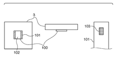
추가적인 얼라인먼트 스코프를 사용하는 글로벌 얼라인먼트 방법에 대해 하기에서 설명할 것이다. 이 방법은 임프린트 장치의 개략도인 도 1을 사용하여 설명할 것이다. 이 임프린트 장치에서는, 웨이퍼 스테이지(1)를 구동시키면서, 오프-액시스 스코프(9)가, 기판 스테이지(웨이퍼 스테이지)(1)에 탑재된 웨이퍼(2) 상의 복수의 샷들에 있는 얼라인먼트 마크들(도시하지 않음)을 계측한다. 임프린트 장치는, 계측한 복수의 얼라인먼트 마크들을 통계 처리해서 웨이퍼(2) 상의 모든 샷들을 맵핑하고, 그 후 어떠한 얼라인먼트 계측도 행하지 않고 임프린트 처리를 행한다. 오프-액시스 스코프(9)는 템플릿(3)을 유지하는 헤드(4)의 외측에 배치되기 때문에, 헤드(4) 내에 배치된 검출기들(스코프들)(5)과는 달리 충분한 공간을 갖는다. 이 때문에 큰 광학계를 구성할 수 있다. 그로 인해, 오프-액시스 스코프(9)는 일반적으로 조명 변화 σ을 갖고, 파장 선택이 가능하고, 고 렌즈 개구를 갖고, 고배율에서 명 시야와 암 시야의 전환이 가능하다는 등의 프로세스 대응력을 갖는 광학계이다.A global alignment method using additional alignment scopes will be described below. This method will be described using FIG. 1, which is a schematic diagram of an imprint apparatus. In this imprint apparatus, while driving the
글로벌 얼라인먼트 방법에서는, 템플릿(3)의 중심과 오프-액시스 스코프(9)의 중심 간의 거리(베이스라인)를 항상 캘리브레이션해야 할 필요가 있다. 이 캘리브레이션을 행하기 위해, 헤드(4)의 스코프(5)는 웨이퍼(2) 상의 각 샷의 얼라인먼트 마크와 템플릿(3) 상에 배치된 얼라인먼트 마크를 검출해서, 템플릿(3)의 중심과 웨이퍼(2) 상의 샷 중심의 상대 위치들을 계측한다. 템플릿(3)의 중심과 웨이퍼(2) 상의 샷 중심의 상대 위치들은, 두 얼라인먼트 마크들을 서로 근접시킬 때 발생하는 무아레 신호로부터 계측된다. 대안적으로, 스코프들(5)이 웨이퍼 스테이지(1) 상의 스테이지 기준 마크(8)와 템플릿(3)의 얼라인먼트 마크의 상대 위치들을 측정한 후, 오프-액시스 스코프(9) 아래에 스테이지 기준 마크(8)가 보내지고, 오프-액시스 스코프(9)가 스테이지 기준 마크(8)를 측정한다. 이 방법들에 의해, 템플릿(3)과 오프-액시스 스코프(9)의 상대 위치들(소위, 베이스라인 량)을 계측할 수 있다. 이 베이스라인 량에 기초하여, 임프린트 장치는 글로벌 얼라인먼트 결과를 템플릿(3) 하에 반영하여 임프린트 처리를 행한다. 제어기(C)는 스코프(5), 웨이퍼 스테이지(1), 수지를 웨이퍼(2)에 토출하는 디스펜서(7) 등을 제어한다. 하기에서, 템플릿 및 임프린트 장치의 실시예들에 대해 첨부 도면을 참조하여 설명할 것이다. In the global alignment method, it is necessary to always calibrate the distance (baseline) between the center of the
<제1 실시예><First Embodiment>
도 2를 참조하여, 임프린트 처리의 과정을 하기에서 설명할 것이다. 템플릿(3)이 수지와 접촉하는 동안에 얼라인먼트는 글로벌 얼라인먼트 방법과 다이-바이-다이 방법 간에 차이가 없기 때문에, 임프린트 처리는 글로벌 얼라인먼트 방법을 기초로 하여 설명한다. S1에서, 임프린트 장치는 오프-액시스 스코프(9)를 사용하여 글로벌 얼라인먼트를 행한다. S2에서, 임프린트 장치는 웨이퍼 스테이지(1)를 구동하여, 웨이퍼(2)의 제1 샷 위치를 디스펜서(7) 아래의 토출 개시 위치로 이동시킨다. S3에서, 임프린트 장치는 웨이퍼 스테이지(1)를 스캔하면서 제1 샷에 수지를 토출한다. S4에서, 임프린트 장치는 웨이퍼 스테이지(1)를 구동하여 제1 샷을 템플릿(3)의 바로 아래 위치로 이동시키고, 압인(임프린트) 단계를 개시한다. 이 압인 단계에 있어서, 노즐들(20)은 산소를 퍼지하기 위해 헬륨(He)을 방출하고, 템플릿(3)과 웨이퍼(2) 사이의 공간을 He으로 충전시킨다. Referring to Fig. 2, the process of the imprint process will be described below. Since the alignment does not differ between the global alignment method and the die-by-die method while the
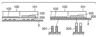
압인 단계에서 수지가 템플릿(3)의 패턴의 오목부들에 충전되는 처리를 하기에서 설명할 것이다. 도 3a 내지 도 3c는 압인의 개시로부터 시간이 경과함에 따라 수지가 템플릿(3)의 패턴 영역 내의 템플릿(3)의 패턴을 형성하는 오목부들에 충전되는 방식을 도시하는 개념도이다. 시간대(time zone) a는, 웨이퍼(2)에 적하된 수지가 템플릿(3)의 패턴 영역에 퍼지는 시간대이다. 시간대 a의 길이는, 적하된 수지와 패턴의 위치들에 따라서도 변화한다. 시간대 a가 종료하면, 임프린트 장치는 템플릿(3)의 오목부들에 수지를 충전하기 시작한다. 도 3a에 도시된 바와 같이, 디바이스 패턴(수지의 패턴) 영역(제1 영역)에 수지가 급격하게 충전된다. 이것은 수지의 표면 장력과, 템플릿(3) 상의 접촉각 및 패턴 크기에 의해 정해지는 모세관력, 및 갇힌 기체(이상적으로는, He만)의 압력 사이의 평형 상태(실제로는 수지의 중력도 가해짐)까지 순간적으로 충전이 진행하기 때문이라고 생각된다. 패턴을 편의상 원으로 가정하면, 모세관압 △P는 수학식 3에 의해 표현된다. 단, T는 표면 장력, θ는 접촉각, r는 패턴 반경이다. A process in which the resin is filled in the recesses of the pattern of the
![]()
![]()
시간대 b는 상기 기체가 수지 중에 용해하는 시간대이다. 시간대 c는 S5의 얼라인먼트 계측을 행할 수 있는 시간대이다. 시각 d는 템플릿(3)의 디바이스 패턴을 형성하는 오목부들에 충전이 종료하는 시각(제1 시각)이다. 시각 d는, 예를 들면, 기체의 마이크로 버블이 수지로부터 소멸하는 것을 고려해서 실험 등에 의해 미리 정해진다. 상술한 바와 같이, 얼라인먼트 마크 영역(제2 영역)에 있어서 템플릿(3)과 샷 사이의 공간이 수지로 충전되거나, 또는 얼라인먼트 마크의 오목부의 대부분이 수지로 충전되어 버리면, 얼라인먼트 마크를 검출하는 것이 곤란하다. 얼라인먼트 검출에는 상이한 위상차를 갖는 광이 필요하다. 오목부의 대부분이 충전되어버리면, 더 이상 위상차가 없어져서, 검출이 곤란해진다. 그러므로, 얼라인먼트 검출에는 어느 정도 충전되어 있지 않은 영역이 필요하다. 얼라인먼트 마크 영역에의 수지의 충전이, 도 3a에 도시된 디바이스 패턴 영역에 수지가 충전될 때와 마찬가지의 방식으로 행해지면, 수지의 충전 중에 얼라인먼트를 할 수 있는 시간은 압인 개시로부터의 초기 단계뿐이다. 즉, 얼라인먼트 마크 영역에 있어서, 디바이스 패턴 영역과 마찬가지의 방식으로 수지가 충전되면, 수지의 충전 동안의 일부 시간대에서만 얼라인먼트 계측을 할 수 있다. 얼라인먼트 마크에 금속막을 부착함으로써, 얼라인먼트 마크 영역에 수지가 존재하는 때에도, 얼라인먼트 마크의 콘트라스트를 유지하는 방법이 제안되어 있다. 그러나, 이 방법은 금속막의 내구성, 템플릿 제조 비용, 및 금속 오염 등과 같은 문제를 갖기 때문에, 실시하기 곤란하다.The time zone b is a time zone in which the gas dissolves in the resin. The time zone c is a time zone in which alignment measurement of S5 can be performed. The time d is the time (first time) at which charging ends in the recesses forming the device pattern of the
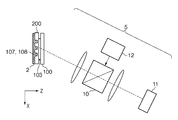
도 3b는 제1 실시예에 따른 수지의 충전을 도시하는 개념도이다. 도 3b에 도시된 제1 실시예에서는, 도 3a에 도시된 것과 비교하면, 시간대 a가 연장되고, 시간대 b의 선단에 있어서의 충전율이 감소된다. 그 결과, 얼라인먼트 계측이 가능한 시간대 c를 충전 종료 시각 d를 초과하도록 연장할 수 있게 된다. 하기에서, 그 상세한 내용에 대해 설명한다. 도 4는 템플릿(3)을 패턴 면으로부터 본 도면과, 템플릿(3)의 측면도와, 얼라인먼트 마크 영역의 확대도를 도시한다. 템플릿(3)은 모체로부터 15 내지 30μm 정도 돌출한 메사(100)라고 불리는 볼록부를 갖고, 이 메사(100)의 표면에 임프린트(압인)될 패턴이 형성되어 있다. 통상, 메사(100)는 디바이스 패턴을 갖는 영역(102)과 스크라이브 영역들(101)을 포함한다. 제1 실시예에 있어서, 스크라이브 영역(101)은 얼라인먼트 마크(103)를 갖는 영역을 포함한다. 도 3a는 디바이스 패턴 영역(102)에 있어서의 충전을 도시하는 개념도이다. 디바이스 패턴 영역(102)에 있어서, 패턴의 폭(패턴 크기)은 하프 피치가 몇십 nm로 매우 작고, 그 때문에 모세관압은 크고 수지의 충전 속도는 빠르다. 수지가 충전된 후, 마이크로 버블 등이 0.1/cm2 이하로 될 때까지 충분한 시간이 경과한 시점이 충전 종료 시각으로서 채택된다. 종래에는, 얼라인먼트 마크(103)가 디바이스 패턴의 크기와 같은 작은 크기로 세그먼트화되어, 모세관압을 증가시키고, 샷 전체의 충전 시간을 단축시킴으로써, 처리량을 증가시킨다. 도 5a는 이 방법을 도시한다. 디바이스 패턴 영역(102)과 세그먼트화된 얼라인먼트 마크(103)에서는, 확대된 오목부(201)에 의해 나타낸 바와 같이 거의 동일한 충전 속도로 수지(200)의 충전이 완료된다. 3B is a conceptual diagram showing the filling of the resin according to the first embodiment. In the first embodiment shown in FIG. 3B, compared with that shown in FIG. 3A, the time zone a is extended, and the filling rate at the tip of the time zone b is reduced. As a result, the time zone c in which alignment measurement is possible can be extended to exceed the charge end time d. Below, the detail is demonstrated. 4 shows a view of the
이에 반해, 도 5b는 얼라인먼트 마크(103)의 패턴의 오목부(202)의 최소 폭이 디바이스 패턴(102)의 복수의 오목부(201)의 최대 폭보다도 크도록 패턴 면이 형성되는 방식을 도시한다. 도 5b에 도시된 바와 같이, 패턴 크기를 크게 한 얼라인먼트 마크(103)의 오목부(202)에서는, 디바이스 패턴(102)의 오목부(201)에의 수지의 충전이 완료된 때에도, 아직 수지의 충전이 완료되지 않는다. 얼라인먼트 마크(103)의 패턴의 크기는, 충전 시간에도 의존하겠지만, 디바이스 패턴(102)의 패턴 크기보다 1 자리 정도 이상 크게 하는 것이 적당하다. In contrast, FIG. 5B illustrates the manner in which the pattern surface is formed such that the minimum width of the
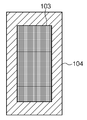
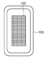
또한, 도 5c는 얼라인먼트 마크(103)의 패턴의 오목부(203)의 최소 깊이가, 디바이스 패턴(102)의 복수의 오목부(201)의 최대의 깊이보다도 깊도록 패턴 면이 형성되는 방식을 도시한다. 도 5c에 도시된 바와 같이, 디바이스 패턴(102)의 오목부(201)보다도 깊은 오목부(203)를 갖는 얼라인먼트 마크(103)를 형성함으로써, 얼라인먼트 마크 영역에서의 충전 시간을 연장할 수 있다. 오목부(203)의 깊이는 얼라인먼트 계측 파장, 및 기타 굴절률 등과 같은 다른 광학 조건들에 의존한다. 그러나, 시뮬레이션에 의하면, 오목부(203)의 깊이는 검출광량의 관점에서 반파장 정도의 깊이인 것이 유리하다. 또한, 도 6a에 도시된 바와 같이, 패턴의 크기가 작고 얼라인먼트 마크(103)보다도 수지가 충전되기 쉬운 제3 패턴(더미 패턴)(104)이 얼라인먼트 마크(103)를 포위하도록 형성될 수 있다. 이러한 더미 패턴(104)은 얼라인먼트 마크(103)에 공급되어야 할 수지가 주변의 더미 패턴(104)으로 더 쉽게 흐르기 때문에, 얼라인먼트 마크(103)에서의 수지의 충전 속도를 감소시킨다. 그 결과, 시간대 a가 연장되고, 시간대 b의 선단에 있어서의 수지의 충전율이 감소되고, 얼라인먼트 계측이 가능한 시간대 c가 연장된다. 또한, 도 6b에 도시된 바와 같이, 얼라인먼트 마크(103)를 포위하는 큰 폭의 홈(105)을 갖는 영역(제3 영역)이 형성될 수 있다. 도 6b에 도시된 얼라인먼트 마크를 사용하는 경우, 제어기(C)는, 디스펜서(7)가 웨이퍼(2)의 디바이스 패턴 영역에 수지를 토출하도록 제어한다. 웨이퍼(2)의 디바이스 패턴 영역에 토출된 수지에 대해 템플릿(3)이 가압될 때, 홈(105)의 외측의 수지는, 홈(105)을 넘어 웨이퍼(2)의 얼라인먼트 마크 영역으로 진입한다. 이 수지의 이동에 의해 수지가 얼라인먼트 마크 영역까지 펼쳐지는 시간대 a를 길게 할 수 있게 되고, 그 결과 얼라인먼트 계측이 가능한 시간대 c를 연장할 수 있다. 상술한 일련의 방법들에서는, 토출된 액적의 배치나 양도 중요한 팩터가 된다. 이상에서는, 도 3b에 도시된 압인 단계에 있어서 얼라인먼트 마크 영역에의 수지의 충전을 위한 템플릿에 대해 설명했다. 이 경우들에 있어서, 얼라인먼트 마크 영역(제2 영역)의 오목부들(201)이 수지로 충전되는 시각(제2 시각)은, 디바이스 패턴 영역(제1 영역)의 오목부들(201)이 수지로 충전되는 시각(제1 시각)보다 나중이다. 따라서, 스코프(5)는, 디바이스 패턴의 오목부들(201)이 수지로 충전되는 제1 시각과 얼라인먼트 마크의 오목부들(201)이 수지로 충전되는 제2 시각 사이에 얼라인먼트 마크(103)를 검출함으로써, 얼라인먼트 마크를 확실하게 검출할 수 있다. 5C shows the manner in which the pattern surface is formed such that the minimum depth of the
하기에서, 템플릿(3)에 형성된 얼라인먼트 마크(103)를 검출하는 스코프(5)에 대해 도 7을 참조하여 설명할 것이다. 웨이퍼(2) 상의 얼라인먼트 마크(웨이퍼 마크)(120)와 템플릿(3) 상의 얼라인먼트 마크(템플릿 마크)(103)는 그들 사이에 수지(200)를 샌드위치하며 서로에 근접하고 있다. 스코프(5)의 광원(12)으로부터 출사되고, 합성 프리즘(10)에 의해 동축 상에 합성되는 계측광은 웨이퍼 마크(120)를 조사한다. 웨이퍼 마크(120)와 템플릿 마크(103)는, 이 마크들의 상대 위치들에 의해 무아레 신호가 발생하도록, 상이한 피치들을 갖는 격자 마크들을 형성한다. 패턴 형상으로서는 도 8에 도시된 마크(106)가 사용된다. 마크(106)는 두개의 상이한 피치 P1, P2를 갖고, 웨이퍼 마크(120)는, 유사한 마크(106)를 회절광이 X 방향으로 전파하도록 배치시킴으로써 형성된다. 그러나, 템플릿측과 웨이퍼측의 대응하는 마크 피치들은 서로 상이하게 만들어진다. 피치 P1을 갖는 템플릿 마크(103)에 대향하는 웨이퍼 마크(120)는 피치 P2를 가져야 한다. 이 두 개의 세트의 마크들에 의해 발생된 두 개의 무아레 신호는 스코프(5)의 결상 광학계를 통과하여, 촬상 소자(11)에 상들을 결상한다. 합성 프리즘(10)으로서는, 하프 미러를 사용할 수 있거나, 또는 계측 광으로서 편광을 사용함으로써 편광 빔 스플리터를 사용할 수 있다. 템플릿 마크(103)와 웨이퍼 마크(120) 간의 위치 관계에 의해 발생되는 두 개의 무아레 신호로부터 앞서 설명한 바와 같이 템플릿(3)의 상대 위치를 구할 수 있다. 그리고, 보정량을 장치에 피드백함으로써, 얼라인먼트 동안, 항상 얼라인먼트 어긋남의 보정 구동이 수행될 수 있다. 또한, 복수 개의 스코프(5)를 임프린트 장치 내에 설치하고, 스코프들(5)의 관찰 위치에 대응하는 복수개의 템플릿 마크(103)를 배치함으로써, 템플릿(3)의 변형도 계측할 수 있다. 보정 구동으로서는 웨이퍼 스테이지(1)의 구동 및 템플릿(3)의 변형을 보정하는 보정 유닛(21)이 클로즈드 보정을 행한다. 보정 유닛(21)은, 예를 들어, 템플릿(3)에 인가되는 압력을 변경함으로써 템플릿(3)의 변형을 보정한다.In the following, the
S6에서 소정 시간이 경과해서 충전이 종료하는 시각 d가 되면, 프로세스는 S7로 진행하여, 임프린트 장치가 즉시 조명계(6)로 자외선(UV)을 조사해서 수지를 경화시킨다. 이 UV 광을 이용하는 수지의 경화 단계에서, 상기 보정 구동은 정지된다. 조명계(6)는 미경화 수지를 경화하는 광을 미경화 수지에 조사하는 조명 유닛이다. UV 조사가 완료되면, S8의 이형 단계에서, 패턴이 전사된 수지로부터 템플릿(3)이 분리되고, 프로세스는 S9에서 다음 샷에 대한 임프린트 처리로 진행한다. 그 후, 상술한 일련의 단계들을 모든 샷들에 대하여 반복한다.When a predetermined time has elapsed in S6 and the time d at which charging is completed, the process proceeds to S7, where the imprint apparatus immediately irradiates ultraviolet (UV) light with the illumination system 6 to cure the resin. In the curing step of the resin using this UV light, the correction drive is stopped. The illumination system 6 is an illumination unit which irradiates the uncured resin with the light which hardens uncured resin. When the UV irradiation is completed, in the release step of S8, the
<제2 실시예>Second Embodiment
제2 실시예에서는, 얼라인먼트 마크(103)의 계측 단계(S5)에서 사용하는 스코프(5)가 제1 실시예의 것과 상이하다. 도 9는 경사 조명에 의해 얼라인먼트 마크(103)를 계측하는 제2 실시예의 스코프(5)의 확대도이다. 경사 조명 스코프(5)의 한가지 장점은 조명계(6)와의 간섭을 피하는 것이다. 웨이퍼(2) 상의 웨이퍼 마크(120)를 형성하는 마크들(107, 108)과, 템플릿 마크(103)는 그들 사이에 수지(200)를 샌드위치하며 서로에 근접하고 있다. 광원(12)으로부터 방출되어 합성 프리즘(10)에 의해 동축 상에 합성된 광은 마크들(107, 108)을 조명한다. 마크들(107, 108)과 템플릿 마크(103)는, 이 마크들의 상대 위치들에 의해 무아레 신호를 발생하도록, 상이한 피치들을 갖는 격자 마크들을 형성한다. 이 구성에서, 경사 조명으로 마크들(107, 108)에 의해 회절된 광은 스코프(5)의 광축으로 복귀하여야 한다. 따라서, 도 8에 도시된 바와 같이, 마크들(107, 108)의 피치 Py를 조정하여, Y 방향으로 전파하는 회절 광을 스코프(5)의 광축으로 복귀하게 한다. 피치 Py는 스코프(5)에 사용되는 계측 광의 파장에 의존하기 때문에, 피치 Py는 설계에 피드백되어야 한다. 마크들(107, 108)은, 상술한 마크(106)와 마찬가지로, 상이한 피치 P1x 및 P2x를 갖는 2 종류의 마크들을 포함한다. 또한, 템플릿 마크로서의 마크(106)의 피치 P1과 P2 간의 관계는, 제1 실시예와 마찬가지로, 마크들(107, 108)의 피치 P1x와 P2x 간의 관계와 역으로 되도록 설계된다. 마크(107)와 마크(108) 간의 차이는, 무아레 신호에 0차 회절광이 혼입되는지의 여부이며, 마크(108)와 같은 지그재그 형상의 패턴을 사용함으로써 0차 광을 캔슬할 수 있다. 0차 광을 캔슬할 때, 무아레 신호는 두 광속에 의해 얻어진 한 개의 주파수만을 갖는다. 이것은 신호 처리를 간단하게 하고 정밀도를 증가시킨다. 이렇게 발생된 두 개의 무아레 신호는 스코프(5)의 결상 광학계를 통해 촬상 소자(11) 상에 결상한다. 사용되는 스코프(5)를 제외한 구성은 제1 실시예의 구성과 마찬가지이므로 설명을 생략한다.In the second embodiment, the
<제3 실시예>Third Embodiment
제1 및 제2 실시예에서, 템플릿(3)의 위치 어긋남 또는 변형은 웨이퍼 마크(120)와 템플릿 마크(103) 간의 위치 어긋남으로부터 계측되고, 계측된 위치 어긋남 또는 변형이 보정된다. 그러나, 제1 및 제2 실시예는, 예를 들어 스테이지 기준 마크(8) 이외에도 웨이퍼 마크(120)가 항상 필요하다는 것과, 또한 무아레 얼라인먼트의 프로세스 대응력이 오프-액시스 얼라인먼트의 것보다도 낮다는 등의 문제가 있다. 이 문제들을 해결하기 위해, 웨이퍼 마크(120) 대신, 스코프(5) 내에 형성된 기준 마크를 참조하여 템플릿 마크(103)의 위치 어긋남을 계측하는 방법이 있다.In the first and second embodiments, the positional shift or deformation of the
도 10에 도시된 바와 같이, 템플릿 마크(103)와 광학적 공액 위치에 기준 마크로서 슬릿(13)을 광원(12)과 템플릿(3) 사이에 삽입한다. 슬릿(13)은 두 개의 상이한 피치 P1'과 P2'를 갖는 회절 슬릿이다. 광원(12)으로부터 출사되어 슬릿(13)을 통과한 계측 광은, 합성 프리즘(10)에 의해 결상 광학계에 유도되어, 템플릿 마크(103)(마찬가지로 두 개의 상이한 피치를 갖는 마크) 상에 투영된다. 서로 대향하는 템플릿 마크(103)와 슬릿(13)의 두개의 세트의 상들은 피치들 간에 반대의 관계를 갖도록 설계된다. 템플릿 마크(103)는 웨이퍼(2)와의 사이에 수지(200)를 샌드위치하며 웨이퍼에 근접하고 있다. 웨이퍼(2)의 기판에는 마크가 존재하지 않는다. 제1 실시예에서와 같이, 템플릿 마크(103)를 계측할 때, 템플릿 마크(103)의 오목부들에는 수지(200)가 충전되지 않기 때문에, 수지(200)와 접촉하지 않는 템플릿 마크(103)의 오목부들만에 의해 상기 슬릿 상이 반사된다. 그리고, 슬릿 상과 템플릿 마크(103)의 무아레 회절광은 스코프(5) 내의 결상 광학계에 유도된다. 무아레 회절광은 스코프(5) 내의 결상 광학계를 통과하고, 촬상 소자(11) 상에 무아레 상을 결상한다. 결상된 두 세트의 무아레 신호가 동시에 관찰된다. 슬릿(13)의 상과 템플릿 마크(103) 간의 상대 위치 관계에 기초하여, 템플릿(3)의 상대 위치 관계를 산출할 수 있다. 더 구체적으로, 슬릿(13)을 기초로 템플릿(3)의 위치 어긋남 및 변형을 항상 계측할 수 있으며, 즉 수지가 토출되지 않은 때라도 계측할 수 있다. 제3 실시예에서는, 항상 템플릿(3)이 계측될 수 있기 때문에, 수지가 토출되지 않은 때에도 템플릿(3)의 보정 구동을 행할 수 있다.As shown in FIG. 10, a
<제4 실시예><Fourth Embodiment>
제4 실시예에서는, 제3 실시예의 것과 동일한 스코프(5)가 설치되어 템플릿(3)에 대하여 경사 조명을 행한다. 나머지 구성은 제3 실시예와 동일하므로 반복적인 설명을 생략한다. 본 실시예에 있어서도, 제3 실시예와 마찬가지로, 슬릿(13)을 기초로 템플릿(3)의 위치 어긋남 및 변형을 항상 계측할 수 있으며, 즉 수지가 토출되지 않은 때라도 계측할 수 있다. 또한, 템플릿(3)이 항상 계측될 수 있기 때문에, 수지가 토출되지 않은 때에도 템플릿(3)의 보정 구동을 행할 수 있다.In the fourth embodiment, the
<제5 실시예> <Fifth Embodiment>
도 3c는 제5 실시예에 있어서의 수지의 충전을 도시하는 개념도이다. 본 실시예의 특징은, 시간대 b에 있어서 He이 수지에 용해하는 동안, 예를 들면 He의 용해를 방해하거나 또는 모세관력을 약화시킴으로써 수지의 충전을 억제 또는 정지시키는 것이다. 도 3c는 특정 시각으로부터 충전이 정지하는 것을 도시하지만, 도 3c은 단지 개념도이고, 본 실시예의 목적은 충전 속도를 감소시킴으로써, 소정의 충전 종료 시각 d에 대하여 얼라인먼트 계측 가능 시간 c를 대폭 연장시키는 것이다.3C is a conceptual diagram showing the filling of the resin in the fifth embodiment. The feature of the present embodiment is to suppress or stop the filling of the resin during the time zone b while He is dissolved in the resin, for example, by impeding the dissolution of He or weakening the capillary force. Although FIG. 3C shows that charging stops from a specific time point, FIG. 3C is only a conceptual diagram, and the purpose of this embodiment is to significantly extend the alignment measurement time c for a predetermined charge end time d by reducing the charging speed. .
S1로부터 S4까지의 단계들은 제1 실시예의 것들과 마찬가지이다. S5에서, 프로세스는 얼라인먼트 단계로 진행한다. 얼라인먼트 단계에서, 도 11a에 도시된 바와 같이, 스코프(5)는 얼라인먼트 마크 계측 광으로서 UV 광을 출사한다. 도 7에 도시된 바와 같이, 웨이퍼 마크(120)와 템플릿(103)에 의해 생성된 무아레 회절광에 의해 템플릿(3)의 위치 어긋남 및 변형을 계측하고, 계측된 템플릿(3)의 위치 어긋남 및 변형을 클로우즈드 루프에 의해 보정한다. 스코프(5)의 광원(12)으로부터 출사되는 UV 광의 파장은, 조명계(6)가 조사하는 광의 파장과 동일한 것이거나, 또는 수지(200)가 가교 반응을 일으키는 파장 대역에 존재하는 것이라면 임의의 파장일 수 있다. 따라서, 스코프(5)는 상기 UV 광의 파장을 갖도록 설계된다. The steps from S1 to S4 are the same as those in the first embodiment. In S5, the process goes to the alignment step. In the alignment step, as shown in FIG. 11A, the
스코프(5)로부터 조사된 UV 광의 조사 영역은 템플릿 마크(103)의 영역으로만 한정되고 있어서, 수지(200)의 경화는 웨이퍼 마크(120)와 템플릿 마크(103) 사이에 샌드위치되는 영역에서 진행한다. 따라서, 템플릿 마크(103)의 영역을 제외한 영역들에서는 수지의 충전이 진행되지만, 템플릿 마크(103)의 영역에서는 수지의 충전이 느려지거나 또는 정지된다. 스코프(5)에 의한 UV 조사의 타이밍은 수지의 UV 경화 속도, 수지의 확산 속도, 및 수지의 충전 속도 사이의 관계에 의존한다. 그러나, 템플릿 마크(103)의 전체 영역에 수지(200)가 퍼지기 전에 UV 조사가 행해지면, 수지가 불균일하게 경화하고, 이것은 종종 얼라인먼트 계측의 에러를 유발하거나 또는 원활한 이형을 방해한다. 따라서, 템플릿 마크(103)의 전체 영역에 수지(200)가 충분히 퍼진 시각으로부터 템플릿 마크(103)의 오목부들 내에 수지가 충전되는 도중까지의 시간대, 즉 시간대 b가 바람직하다. 그 후, 소정의 충전 시간이 종료하고(S6), 조명계(6)에 의한 UV 경화 단계(S7)가 시작될 때까지 얼라인먼트 계측과, 템플릿의 위치 어긋남 보정 및 변형 보정을 클로우즈드 루프에 의해 행한다. 그런 다음, 프로세스는 제1 실시예의 것과 마찬가지의 이형 이후의 단계들로 진행한다. 제5 실시예에서는, 스코프(5)가 경사 조명 스코프인 경우에도, 제2 실시예와 마찬가지의 방식으로 얼라인먼트 계측 및 보정이 행해질 수 있다. 또한, 제3 및 제4 실시예와 마찬가지로, 템플릿 마크와 기준 슬릿의 얼라인먼트 계측을 행하는 스코프(5)를 사용할 수 있다.The irradiation area of the UV light irradiated from the
<제6 실시예> Sixth Example
제5 실시예에서는, 수지의 충전 속도를 감소시키기 위한 광과 얼라인먼트 마크의 계측 광으로서 UV 광이 사용된다. 제6 실시예에서는, 수지의 충전 속도를 감소시키기 위한 UV 광의 파장과는 상이한 파장의 광이 얼라인먼트 마크의 계측 광으로서 사용된다. 얼라인먼트 마크의 계측 광의 파장에서 수지의 UV 경화가 발생하지 않기 때문에, 얼라인먼트 마크 영역의 수지 경화와 얼라인먼트 계측은 독립적으로 병행하여 행해진다. 이로써, 처리량을 감소시키지 않으면서 더 정확하게 수지의 충전 속도를 제어할 수 있게 된다. In the fifth embodiment, UV light is used as light for reducing the filling speed of the resin and measurement light for alignment marks. In the sixth embodiment, light having a wavelength different from that of the UV light for reducing the filling speed of the resin is used as the measurement light of the alignment mark. Since UV hardening of resin does not generate | occur | produce in the wavelength of the measurement light of alignment mark, resin hardening and alignment measurement of an alignment mark area | region are performed in parallel independently. This makes it possible to more precisely control the filling rate of the resin without reducing the throughput.
S1로부터 S4까지의 단계들은 제1 실시예의 것들과 동일하다. S5에서, 프로세스는 얼라인먼트 단계로 진행한다. 얼라인먼트 단계에서는, 도 11b에 도시된 순서도에 의해 지시된 바와 같이, 스코프(5)의 광원(12)은 계측 광을 출사하고, 제5 실시예와 마찬가지로 얼라인먼트 계측과, 템플릿의 위치 어긋남 보정 및 템플릿 변형 보정을 클로우즈드 루프에 의해 행한다. 그러나, 제6 실시예의 스코프(5)는 얼라인먼트 마크의 계측 광의 파장으로 설계된다. 또한, 후술하는 바와 같이, UV 광의 무아레 회절 광도 동시에 촬상 소자(11)에 혼입된다. 따라서, 계측 정밀도의 관점에서는, 예를 들어 촬상 소자(11)의 직전에 밴드패스 필터를 삽입하는 것 등에 의해 계측 광만을 통과시키는 것이 바람직하다. 스코프(5)의 광원(12)으로부터 출사되는 계측 광의 파장은, 수지(200)가 가교 반응을 일으키지 않는 파장 대역 내로 설정된다. 거의 동시적으로, 별도의 광원이 UV 광을 조사한다. UV 조사는 템플릿 마크(103)의 영역에만 한정되기 때문에, 수지(200)의 경화는 템플릿 마크(103)의 영역에서 진행한다. 또한, 독립으로 UV 조사를 제어함으로써, 수지의 경화 속도를 최적으로 제어할 수 있다. The steps from S1 to S4 are the same as those in the first embodiment. In S5, the process goes to the alignment step. In the alignment step, as indicated by the flow chart shown in FIG. 11B, the
스코프(5)로부터의 UV 조사의 타이밍은, 제5 실시예와 마찬가지로, 템플릿 마크(103)의 전체 영역에 수지(200)가 충분히 퍼진 시각으로부터 템플릿 마크(103)의 각각의 오목부의 깊이로 수지가 충전되는 도중까지의 시간 대인 것이 바람직하다. 얼라인먼트 계측의 타이밍은 특별히 한정되지 않는다. 또한, 이 얼라인먼트 계측 화상을 이용하여 수지(200)의 확산 상태를 감시함으로써, UV 조사의 타이밍을 실시간으로 장치에 피드백할 수 있다. Timing of the UV irradiation from the
제6 실시예에 있어서, 스코프(5)가 경사 조명 스코프인 때라도 제2 실시예와 마찬가지의 방식으로 얼라인먼트 계측 및 보정이 행해질 수 있다. 또한, 제3 및 제4 실시예와 마찬가지로, 템플릿 마크와 기준 슬릿의 얼라인먼트 계측을 행하는 스코프(5)를 사용할 수 있다.In the sixth embodiment, alignment measurement and correction can be performed in the same manner as in the second embodiment even when the
<물품의 제조 방법><Production method of the article>
물품으로서의 디바이스(예를 들면, 반도체 집적 회로 소자 또는 액정 표시 소자)의 제조 방법은, 상술한 임프린트 장치를 사용하여 기판(웨이퍼, 유리 플레이트, 또는 필름 형상 기판)에 패턴을 전사(형성)하는 단계를 포함한다. 이 제조 방법은 패턴이 전사된 기판을 에칭하는 단계를 더 포함할 수 있다. 패터닝된 매체(기록 매체) 또는 광학 소자 등과 같은 다른 물품을 제조하는 경우에는, 상기 제조 방법은 에칭 단계 대신에, 패턴이 전사된 기판을 가공하는 별도의 단계를 포함할 수 있다. 이상, 본 발명의 실시예들이 설명되었지만, 본 발명은 이 실시예들로 한정되지 않고, 본 발명의 사상 및 범위 내에서 여러가지 변형 및 변경이 이루어질 수 있다.A method of manufacturing a device as an article (for example, a semiconductor integrated circuit element or a liquid crystal display element) includes the steps of transferring (forming) a pattern onto a substrate (a wafer, a glass plate, or a film-shaped substrate) using the imprint apparatus described above. It includes. The manufacturing method may further include etching the substrate to which the pattern has been transferred. In the case of manufacturing another article such as a patterned medium (recording medium) or an optical element, the manufacturing method may include a separate step of processing the substrate to which the pattern has been transferred, instead of the etching step. Although the embodiments of the present invention have been described above, the present invention is not limited to these embodiments, and various modifications and changes can be made without departing from the spirit and scope of the present invention.
본 발명이 예시적인 실시예들을 참조하여 설명되었으나, 본 발명은 개시된 실시예들로 한정되지 않는다는 것을 이해하여야 한다. 하기의 청구항들의 범위는 그러한 변형들 및 등가의 구조와 기능들을 모두 포괄하도록 최광의의 해석에 따라야 한다.While the invention has been described with reference to exemplary embodiments, it is to be understood that the invention is not limited to the disclosed embodiments. The scope of the following claims is to be accorded the broadest interpretation so as to encompass all such modifications and equivalent structures and functions.
1: 웨이퍼 스테이지
2: 웨이퍼
3: 템플릿
4: 헤드
5: 검출기(스코프)
6: 조명계
7: 디스펜서
8: 스테이지 기준 마크
9: 오프-액시스 스코프
20: 노즐
21: 보정 유닛
100: 메사
101: 스크라이브 영역
102: 디바이스 패턴 영역
103: 얼라인먼트 마크
104: 더미 패턴
105: 홈
201, 203: 오목부
C: 제어기1: wafer stage
2: wafer
3: template
4: head
5: Detector (scope)
6: lighting system
7: dispenser
8: Stage reference mark
9: off-axis scope
20: nozzle
21: correction unit
100: mesa
101: scribe area
102: device pattern area
103: alignment mark
104: dummy pattern
105: home
201, 203: recess
C: controller
Claims (9)
기판 상에 미경화 수지를 토출하도록 구성된 디스펜서,
템플릿의 패턴 면에 배치된 얼라인먼트 마크를 광을 이용하여 검출하도록 구성된 검출기, 및
제어기를 포함하고,
상기 패턴 면은, 상기 수지의 패턴에 대응하는 패턴을 포함하는 제1 영역과, 상기 얼라인먼트 마크를 포함하는 제2 영역을 포함하고, 또한 상기 제1 영역의 오목부가 미경화 수지로 충전되는 제1 시각보다 상기 제2 영역의 오목부가 미경화 수지로 충전되는 제2 시각이 나중이 되도록 형성되고,
상기 제어기는, 상기 제1 영역의 오목부와 상기 제2 영역의 오목부가 미경화 수지로 충전되는 양의 미경화 수지를 상기 디스펜서가 상기 기판에 토출하게 하고, 상기 제1 시각과 상기 제2 시각 사이에 상기 검출기가 상기 얼라인먼트 마크를 검출하게 하도록 구성된, 임프린트 장치.It is an imprint apparatus comprised so that the imprint process of forming the pattern of resin for manufacture of an article on a board | substrate using an uncured resin and a template,
A dispenser configured to discharge the uncured resin onto the substrate,
A detector configured to detect, using light, an alignment mark disposed on the pattern side of the template, and
Including a controller,
The pattern surface includes a first region including a pattern corresponding to the pattern of the resin and a second region including the alignment mark, and the first recessed portion of the first region is filled with an uncured resin. The second time at which the recessed portion of the second region is filled with the uncured resin is formed later than the time,
The controller causes the dispenser to discharge the uncured resin in an amount of the concave portion of the first region and the concave portion of the second region filled with an uncured resin, and the first time and the second time. And cause the detector to detect the alignment mark in between.
상기 제2 영역의 오목부의 최소의 폭이 상기 제1 영역의 오목부의 최대 폭보다 크도록, 상기 패턴 면이 형성되는, 임프린트 장치. The method of claim 1,
And the pattern surface is formed such that the minimum width of the concave portion of the second region is larger than the maximum width of the concave portion of the first region.
상기 제2 영역의 오목부의 최소 깊이가 상기 제1 영역의 오목부의 최대 깊이보다 크도록, 상기 패턴 면이 형성되는, 임프린트 장치. The method of claim 1,
And the pattern surface is formed such that the minimum depth of the recessed portion of the second region is greater than the maximum depth of the recessed portion of the first region.
상기 패턴 면은 상기 얼라인먼트 마크를 포위하는 제3 패턴을 포함하는 제3 영역을 더 포함하고,
상기 제3 영역의 오목부의 최대 폭이 상기 제2 영역의 오목부의 최소 폭보다 작도록, 상기 패턴 면이 형성되는, 임프린트 장치.The method of claim 1,
The pattern surface further includes a third region including a third pattern surrounding the alignment mark,
And the pattern surface is formed such that the maximum width of the concave portion of the third region is smaller than the minimum width of the concave portion of the second region.
상기 기판 상에 미경화 수지를 토출하도록 구성된 디스펜서,
상기 템플릿의 패턴 면에 배치된 얼라인먼트 마크를 광을 이용하여 검출하도록 구성된 검출기, 및
제어기를 포함하고,
상기 패턴 면은, 상기 수지의 패턴에 대응하는 패턴을 포함하는 제1 영역과, 상기 얼라인먼트 마크를 포함하는 제2 영역, 및 상기 얼라인먼트 마크를 포위하는 홈(moat)을 포함하는 제3 영역을 포함하고,
상기 제어기는, 상기 제1 영역의 오목부와, 상기 제2 영역의 오목부, 및 상기 제3 영역의 오목부가 미경화 수지로 충전되는 양의 미경화 수지를 상기 디스펜서가 상기 제1 영역에 토출하게 하고, 또한 상기 제1 영역의 오목부가 미경화 수지로 충전되는 제1 시각과, 상기 제3 영역의 오목부가 상기 제1 영역으로부터 상기 제2 영역쪽으로 이동한 미경화 수지로 충전되는 제2 시각 사이에 상기 검출기가 상기 얼라인먼트 마크를 검출하게 하도록 구성된, 임프린트 장치. It is an imprint apparatus comprised so that the imprint process which forms the pattern of resin for manufacture of an article on a board | substrate using an uncured resin and a template,
A dispenser configured to discharge an uncured resin on the substrate,
A detector configured to detect, using light, an alignment mark disposed on the pattern surface of the template, and
Including a controller,
The pattern surface includes a first region including a pattern corresponding to the pattern of the resin, a second region including the alignment mark, and a third region including a moat surrounding the alignment mark. and,
The controller discharges the uncured resin in the first region, the concave portion of the second region, and the amount of the uncured resin filled with the uncured resin into the first region. And a first time when the recessed portion of the first region is filled with an uncured resin, and a second time when the recessed portion of the third region is filled with an uncured resin moved from the first region toward the second region. And cause the detector to detect the alignment mark in between.
상기 기판 상에 미경화 수지를 토출하도록 구성된 디스펜서,
상기 템플릿의 패턴 면에 배치된 얼라인먼트 마크를 광을 이용하여 검출하도록 구성된 검출기,
미경화 수지를 경화시키는 광을 미경화 수지에 조사하도록 구성된 조사 유닛, 및
제어기를 포함하고,
상기 패턴 면은, 상기 수지의 패턴에 대응하는 패턴을 포함하는 제1 영역, 및 상기 얼라인먼트 마크를 포함하는 제2 영역을 포함하고,
상기 제어기는, 상기 제1 영역의 오목부와 상기 제2 영역의 오목부가 미경화 수지로 충전되는 양의 미경화 수지를 상기 디스펜서가 상기 기판에 토출하게 하고, 상기 제2 영역의 오목부에 미경화 수지가 인입한 후, 상기 제2 영역의 오목부가 미경화 수지로 충전되기 전에, 상기 조사 유닛이 상기 제2 영역의 오목부 내의 미경화 수지를 조사해서 경화시키고, 또한, 상기 제2 영역의 오목부 내의 미경화 수지가 경화된 상태에서 상기 검출기가 상기 얼라인먼트 마크를 검출하게 하도록 구성된, 임프린트 장치.It is an imprint apparatus comprised so that the imprint process which forms the pattern of resin for manufacture of an article on a board | substrate using an uncured resin and a template,
A dispenser configured to discharge an uncured resin on the substrate,
A detector configured to detect, using light, an alignment mark disposed on a pattern surface of the template,
An irradiation unit configured to irradiate the uncured resin with light for curing the uncured resin, and
Including a controller,
The pattern surface includes a first region including a pattern corresponding to the pattern of the resin, and a second region including the alignment mark,
The controller causes the dispenser to discharge the uncured resin in an amount of the concave portion of the first region and the concave portion of the second region filled with the uncured resin to the substrate, After the cured resin is introduced, before the concave portion of the second region is filled with the uncured resin, the irradiation unit irradiates and cures the uncured resin in the concave portion of the second region, and further And the detector detects the alignment mark in a state where the uncured resin in the recess is cured.
상기 제1 영역의 오목부가 미경화 수지로 충전된 후, 미경화 수지를 경화하는 광을 상기 제1 영역의 오목부 내의 미경화 수지에 조사하도록 구성된 조사 유닛을 더 포함하는, 임프린트 장치. The method of claim 6,
And an irradiation unit configured to irradiate the uncured resin in the recess of the first region with light for curing the uncured resin after the recess of the first region is filled with the uncured resin.
제1항 내지 제7항 중 어느 한 항에 따른 임프린트 장치를 이용하여 수지의 패턴을 기판에 형성하는 단계, 및
상기 수지의 패턴이 형성된 기판을 가공하여 상기 물품을 제조하는 단계를 포함하는 물품의 제조 방법.The method of making the article,
Forming a pattern of resin on a substrate using the imprint apparatus according to any one of claims 1 to 7,
Manufacturing the article by processing the substrate on which the pattern of resin is formed.
상기 탬플릿은 상기 수지의 패턴에 대응하는 패턴을 포함하는 제1 영역, 및 상기 얼라인먼트 마크를 포함하는 제2 영역을 포함하는 패턴 면을 포함하고,
상기 패턴 면은, 상기 제1 영역의 오목부가 미경화 수지로 충전되는 제1 시각보다 상기 제2 영역의 오목부가 미경화 수지로 충전되는 제2 시각이 나중이 되도록 형성되는, 템플릿. It is a template used for the imprint apparatus comprised by the imprint process which forms the pattern of resin for manufacture of an article on a board | substrate using an uncured resin and a template,
The template includes a first surface including a pattern corresponding to the pattern of the resin, and a pattern surface including a second region including the alignment mark,
The said pattern surface is formed so that the 2nd time when the recessed part of the said 2nd area may be filled with an uncured resin may be later than the 1st time when the recessed part of the said 1st area is filled with an uncured resin.
Applications Claiming Priority (2)
| Application Number | Priority Date | Filing Date | Title |
|---|---|---|---|
| JPJP-P-2010-039203 | 2010-02-24 | ||
| JP2010039203A JP5451450B2 (en) | 2010-02-24 | 2010-02-24 | Imprint apparatus, template thereof, and article manufacturing method |
Publications (1)
| Publication Number | Publication Date |
|---|---|
| KR20110097641A true KR20110097641A (en) | 2011-08-31 |
Family
ID=44168875
Family Applications (1)
| Application Number | Title | Priority Date | Filing Date |
|---|---|---|---|
| KR1020110013709A KR20110097641A (en) | 2010-02-24 | 2011-02-16 | Imprint apparatus, template of imprint apparatus, and article manufacturing method |
Country Status (6)
| Country | Link |
|---|---|
| US (1) | US20110206852A1 (en) |
| EP (1) | EP2360524A2 (en) |
| JP (1) | JP5451450B2 (en) |
| KR (1) | KR20110097641A (en) |
| CN (1) | CN102162992A (en) |
| TW (1) | TW201139118A (en) |
Cited By (2)
| Publication number | Priority date | Publication date | Assignee | Title |
|---|---|---|---|---|
| KR20140119800A (en) * | 2012-03-12 | 2014-10-10 | 캐논 가부시끼가이샤 | Imprint method, imprint apparatus, and article manufacturing method using the same |
| KR20140138845A (en) * | 2012-03-14 | 2014-12-04 | 캐논 가부시끼가이샤 | Imprint apparatus, mold, imprint method, and method of manufacturing article |
Families Citing this family (41)
| Publication number | Priority date | Publication date | Assignee | Title |
|---|---|---|---|---|
| JP5618663B2 (en) * | 2010-07-15 | 2014-11-05 | 株式会社東芝 | Imprint template and pattern forming method |
| JP2013074115A (en) * | 2011-09-28 | 2013-04-22 | Fujifilm Corp | Nanoimprint device and nanoimprint method, and strain application device and strain application method |
| JP5686779B2 (en) | 2011-10-14 | 2015-03-18 | キヤノン株式会社 | Imprint apparatus and article manufacturing method using the same |
| JP6159072B2 (en) * | 2011-11-30 | 2017-07-05 | キヤノン株式会社 | Imprint apparatus, imprint method, and article manufacturing method |
| JP5868215B2 (en) * | 2012-02-27 | 2016-02-24 | キヤノン株式会社 | Imprint apparatus, imprint method, and article manufacturing method using the same |
| JP6060796B2 (en) * | 2013-04-22 | 2017-01-18 | 大日本印刷株式会社 | Imprint mold and dummy pattern design method |
| JP6361238B2 (en) * | 2013-04-23 | 2018-07-25 | 大日本印刷株式会社 | Imprint mold and imprint method |
| JP2014229670A (en) * | 2013-05-20 | 2014-12-08 | 株式会社東芝 | Pattern forming method and pattern forming device |
| JP6282069B2 (en) * | 2013-09-13 | 2018-02-21 | キヤノン株式会社 | Imprint apparatus, imprint method, detection method, and device manufacturing method |
| KR101777905B1 (en) * | 2013-10-17 | 2017-09-12 | 캐논 가부시끼가이샤 | Imprint apparatus, and method of manufacturing article |
| JP6541328B2 (en) * | 2013-11-26 | 2019-07-10 | キヤノン株式会社 | Detection apparatus, imprint apparatus, and method of manufacturing article |
| JP6294680B2 (en) | 2014-01-24 | 2018-03-14 | キヤノン株式会社 | Imprint apparatus and article manufacturing method |
| JP5932859B2 (en) | 2014-02-18 | 2016-06-08 | キヤノン株式会社 | Detection apparatus, imprint apparatus, and article manufacturing method |
| JP2015170815A (en) * | 2014-03-10 | 2015-09-28 | キヤノン株式会社 | Imprint device, alignment method, and manufacturing method for article |
| US10265724B2 (en) | 2014-04-01 | 2019-04-23 | Dai Nippon Printing Co., Ltd. | Imprint mold and imprint method |
| JP6415120B2 (en) * | 2014-06-09 | 2018-10-31 | キヤノン株式会社 | Imprint apparatus and article manufacturing method |
| JP6420571B2 (en) * | 2014-06-13 | 2018-11-07 | キヤノン株式会社 | Imprint apparatus, imprint method, and article manufacturing method |
| JP6394114B2 (en) * | 2014-06-27 | 2018-09-26 | 大日本印刷株式会社 | Template manufacturing method and template |
| JP6076946B2 (en) * | 2014-08-04 | 2017-02-08 | 大日本印刷株式会社 | Roller imprint mold and imprint method, wire grid polarizer and method of manufacturing the same |
| JP6472189B2 (en) * | 2014-08-14 | 2019-02-20 | キヤノン株式会社 | Imprint apparatus, imprint method, and article manufacturing method |
| JP6632270B2 (en) * | 2014-09-08 | 2020-01-22 | キヤノン株式会社 | Imprint apparatus, imprint method, and article manufacturing method |
| JP6429573B2 (en) * | 2014-10-03 | 2018-11-28 | キヤノン株式会社 | Imprint apparatus, imprint method, and article manufacturing method |
| JP6549834B2 (en) * | 2014-11-14 | 2019-07-24 | キヤノン株式会社 | Imprint apparatus and method of manufacturing article |
| JP6674218B2 (en) * | 2014-12-09 | 2020-04-01 | キヤノン株式会社 | Imprint apparatus, imprint method, and article manufacturing method |
| US10747106B2 (en) | 2014-12-09 | 2020-08-18 | Canon Kabushiki Kaisha | Imprint apparatus |
| JP6525628B2 (en) * | 2015-02-13 | 2019-06-05 | キヤノン株式会社 | Imprint apparatus and method of manufacturing article |
| JP6700794B2 (en) * | 2015-04-03 | 2020-05-27 | キヤノン株式会社 | Imprint material discharge device |
| JP6685821B2 (en) * | 2016-04-25 | 2020-04-22 | キヤノン株式会社 | Measuring apparatus, imprint apparatus, article manufacturing method, light quantity determination method, and light quantity adjustment method |
| JP2016149578A (en) * | 2016-05-11 | 2016-08-18 | 大日本印刷株式会社 | Production method of replica template for nanoimprinting |
| WO2017204260A1 (en) * | 2016-05-25 | 2017-11-30 | 大日本印刷株式会社 | Template, template blank and imprint template board making method, imprint template making method, and template |
| JP2017034276A (en) * | 2016-10-20 | 2017-02-09 | 大日本印刷株式会社 | Mold for imprint and imprint method |
| US11175598B2 (en) * | 2017-06-30 | 2021-11-16 | Canon Kabushiki Kaisha | Imprint apparatus and method of manufacturing article |
| JP7089348B2 (en) | 2017-07-28 | 2022-06-22 | キヤノン株式会社 | Imprint device, imprint method and article manufacturing method |
| JP7027099B2 (en) * | 2017-09-29 | 2022-03-01 | キヤノン株式会社 | Manufacturing method of imprint device and goods |
| JP6579217B2 (en) * | 2018-04-24 | 2019-09-25 | 大日本印刷株式会社 | Template manufacturing method and template |
| US10759116B2 (en) * | 2018-09-14 | 2020-09-01 | Intrepid Automation | Additive manufactured parts with smooth surface finishes |
| JP7278135B2 (en) * | 2019-04-02 | 2023-05-19 | キヤノン株式会社 | Imprint apparatus and article manufacturing method |
| JP7374666B2 (en) * | 2019-08-29 | 2023-11-07 | キヤノン株式会社 | Imprint method, pretreatment device, imprint substrate, and substrate manufacturing method |
| JP7384012B2 (en) | 2019-12-05 | 2023-11-21 | 大日本印刷株式会社 | Imprint mold and its manufacturing method, and imprint method |
| CN112835276A (en) * | 2020-12-31 | 2021-05-25 | 合肥芯碁微电子装备股份有限公司 | Alignment system, control method thereof and laser direct-writing exposure equipment |
| CN113314451B (en) * | 2021-06-10 | 2022-08-02 | 哈尔滨工业大学 | Wafer bonding alignment system and method based on moire fringes |
Family Cites Families (13)
| Publication number | Priority date | Publication date | Assignee | Title |
|---|---|---|---|---|
| EP2264523A3 (en) * | 2000-07-16 | 2011-11-30 | Board Of Regents, The University Of Texas System | A method of forming a pattern on a substrate in imprint lithographic processes |
| US6926929B2 (en) * | 2002-07-09 | 2005-08-09 | Molecular Imprints, Inc. | System and method for dispensing liquids |
| US7309225B2 (en) * | 2004-08-13 | 2007-12-18 | Molecular Imprints, Inc. | Moat system for an imprint lithography template |
| JP2006165371A (en) * | 2004-12-09 | 2006-06-22 | Canon Inc | Transfer apparatus and device manufacturing method |
| JP2006245072A (en) * | 2005-02-28 | 2006-09-14 | Canon Inc | Mold for transferring pattern and transfer device |
| JP4330168B2 (en) * | 2005-09-06 | 2009-09-16 | キヤノン株式会社 | Mold, imprint method, and chip manufacturing method |
| US7690910B2 (en) * | 2006-02-01 | 2010-04-06 | Canon Kabushiki Kaisha | Mold for imprint, process for producing minute structure using the mold, and process for producing the mold |
| JP4185941B2 (en) | 2006-04-04 | 2008-11-26 | キヤノン株式会社 | Nanoimprint method and nanoimprint apparatus |
| CN101059650A (en) * | 2006-04-18 | 2007-10-24 | 佳能株式会社 | Pattern transfer printing device, stamping device and pattern transfer printing method |
| JP4819577B2 (en) * | 2006-05-31 | 2011-11-24 | キヤノン株式会社 | Pattern transfer method and pattern transfer apparatus |
| JP5061525B2 (en) * | 2006-08-04 | 2012-10-31 | 株式会社日立製作所 | Imprint method and imprint apparatus |
| JP5404140B2 (en) * | 2009-04-01 | 2014-01-29 | 株式会社東芝 | Template and semiconductor device manufacturing method |
| NL2004932A (en) * | 2009-07-27 | 2011-01-31 | Asml Netherlands Bv | Imprint lithography template. |
-
2010
- 2010-02-24 JP JP2010039203A patent/JP5451450B2/en not_active Expired - Fee Related
-
2011
- 2011-01-18 EP EP11151246A patent/EP2360524A2/en not_active Withdrawn
- 2011-01-24 TW TW100102490A patent/TW201139118A/en unknown
- 2011-02-16 KR KR1020110013709A patent/KR20110097641A/en not_active Application Discontinuation
- 2011-02-21 CN CN2011100417603A patent/CN102162992A/en active Pending
- 2011-02-23 US US13/033,362 patent/US20110206852A1/en not_active Abandoned
Cited By (5)
| Publication number | Priority date | Publication date | Assignee | Title |
|---|---|---|---|---|
| KR20140119800A (en) * | 2012-03-12 | 2014-10-10 | 캐논 가부시끼가이샤 | Imprint method, imprint apparatus, and article manufacturing method using the same |
| US20150325526A1 (en) * | 2012-03-12 | 2015-11-12 | Canon Kabushiki Kaisha | Imprint method, imprint apparatus, and article manufacturing method using the same |
| US10901324B2 (en) | 2012-03-12 | 2021-01-26 | Canon Kabushiki Kaisha | Imprint method, imprint apparatus, and article manufacturing method using the same |
| KR20140138845A (en) * | 2012-03-14 | 2014-12-04 | 캐논 가부시끼가이샤 | Imprint apparatus, mold, imprint method, and method of manufacturing article |
| US9921470B2 (en) | 2012-03-14 | 2018-03-20 | Canon Kabushiki Kaisha | Imprint method for an imprint apparatus which transfers a pattern onto a substrate by using a mold |
Also Published As
| Publication number | Publication date |
|---|---|
| TW201139118A (en) | 2011-11-16 |
| JP2011176132A (en) | 2011-09-08 |
| JP5451450B2 (en) | 2014-03-26 |
| US20110206852A1 (en) | 2011-08-25 |
| CN102162992A (en) | 2011-08-24 |
| EP2360524A2 (en) | 2011-08-24 |
Similar Documents
| Publication | Publication Date | Title |
|---|---|---|
| JP5451450B2 (en) | Imprint apparatus, template thereof, and article manufacturing method | |
| KR101842394B1 (en) | Imprinting method, imprinting apparatus, and article manufacturing method | |
| KR101435250B1 (en) | Mold, imprint method, and method of manufacturing article | |
| JP6884515B2 (en) | Position detection method, imprinting device and article manufacturing method | |
| JP6415120B2 (en) | Imprint apparatus and article manufacturing method | |
| US10732523B2 (en) | Detection device, imprint apparatus, method of manufacturing article, illumination optical system, and detection method | |
| US9910351B2 (en) | Imprint apparatus and article manufacturing method | |
| JP2017199725A (en) | Measuring device, imprint device, method of manufacturing article, method of determining amount of light, and method of adjusting amount of light | |
| US20160207248A1 (en) | Imprint apparatus, imprinting method, and method of manufacturing articles | |
| JP5669516B2 (en) | Lithographic apparatus and device manufacturing method | |
| JP5709558B2 (en) | Inspection method, imprint apparatus, and article manufacturing method | |
| JP6381721B2 (en) | Imprint method, imprint apparatus and device manufacturing method | |
| JP7433861B2 (en) | Imprint equipment, imprint method, article manufacturing method, substrate, and mold | |
| JP2007250767A (en) | Processing apparatus and method therefor, and manufacturing method of device | |
| JP2012142327A (en) | Imprint apparatus, method, and template for imprint | |
| JP2019158516A (en) | Position detector, position detection method, imprint device, and goods manufacturing method | |
| KR20240002183A (en) | Imprint system, substrate, imprint method, replica mold manufacturing method, and article manufacturing method | |
| JP2020038164A (en) | Position detection device, position detection method, mold, imprint device, and method for manufacturing article |
Legal Events
| Date | Code | Title | Description |
|---|---|---|---|
| A201 | Request for examination | ||
| E601 | Decision to refuse application |