KR20110074841A - Led 프로젝터 - Google Patents
Led 프로젝터 Download PDFInfo
- Publication number
- KR20110074841A KR20110074841A KR1020117000179A KR20117000179A KR20110074841A KR 20110074841 A KR20110074841 A KR 20110074841A KR 1020117000179 A KR1020117000179 A KR 1020117000179A KR 20117000179 A KR20117000179 A KR 20117000179A KR 20110074841 A KR20110074841 A KR 20110074841A
- Authority
- KR
- South Korea
- Prior art keywords
- led
- leds
- layers
- conductive paths
- carrier
- Prior art date
- Legal status (The legal status is an assumption and is not a legal conclusion. Google has not performed a legal analysis and makes no representation as to the accuracy of the status listed.)
- Ceased
Links
- 239000011521 glass Substances 0.000 claims description 23
- 229910052751 metal Inorganic materials 0.000 claims description 21
- 239000002184 metal Substances 0.000 claims description 21
- 238000000034 method Methods 0.000 claims description 11
- 239000003086 colorant Substances 0.000 claims description 10
- XUIMIQQOPSSXEZ-UHFFFAOYSA-N Silicon Chemical compound [Si] XUIMIQQOPSSXEZ-UHFFFAOYSA-N 0.000 claims description 7
- 229910052710 silicon Inorganic materials 0.000 claims description 7
- 239000010703 silicon Substances 0.000 claims description 7
- 239000004020 conductor Substances 0.000 claims description 5
- 238000003384 imaging method Methods 0.000 description 4
- 230000004907 flux Effects 0.000 description 2
- AMGQUBHHOARCQH-UHFFFAOYSA-N indium;oxotin Chemical compound [In].[Sn]=O AMGQUBHHOARCQH-UHFFFAOYSA-N 0.000 description 2
- 239000004973 liquid crystal related substance Substances 0.000 description 2
- 238000000576 coating method Methods 0.000 description 1
- 150000001875 compounds Chemical class 0.000 description 1
- 230000001419 dependent effect Effects 0.000 description 1
- 238000010586 diagram Methods 0.000 description 1
- 230000003287 optical effect Effects 0.000 description 1
- 230000010287 polarization Effects 0.000 description 1
- 238000004382 potting Methods 0.000 description 1
Images


Classifications
-
- G—PHYSICS
- G03—PHOTOGRAPHY; CINEMATOGRAPHY; ANALOGOUS TECHNIQUES USING WAVES OTHER THAN OPTICAL WAVES; ELECTROGRAPHY; HOLOGRAPHY
- G03B—APPARATUS OR ARRANGEMENTS FOR TAKING PHOTOGRAPHS OR FOR PROJECTING OR VIEWING THEM; APPARATUS OR ARRANGEMENTS EMPLOYING ANALOGOUS TECHNIQUES USING WAVES OTHER THAN OPTICAL WAVES; ACCESSORIES THEREFOR
- G03B21/00—Projectors or projection-type viewers; Accessories therefor
- G03B21/14—Details
- G03B21/20—Lamp housings
- G03B21/2006—Lamp housings characterised by the light source
- G03B21/2033—LED or laser light sources
Landscapes
- Physics & Mathematics (AREA)
- Optics & Photonics (AREA)
- General Physics & Mathematics (AREA)
- Led Device Packages (AREA)
- Projection Apparatus (AREA)
Abstract
Description
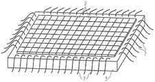
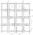
도 1은 LED 어레이의 평면도이다.
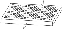
도 2는 캐리어상에 위치한 적층형 에피 LED 장치의 사시도이다.
도 3은 본딩 와이어를 포함한 실시예를 위한, 도 2에 따른 개략도이다.
도 4는 하측의 연결 접촉면을 포함한 실시예의 배면도이다.
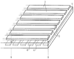
도 5는 라인 어드레싱을 위한 도전로를 포함한 캐리어의 사시도이다.
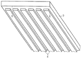
도 6은 라인 어드레싱 및 컬럼 어드레싱을 위한 도전로를 포함한 유리 필름의 사시도이다.
도 7은 컬럼 어드레싱을 위한 도전로를 포함한 유리 필름의 배면 사시도이다.
도 8은 투명한 간극층들 사이에 위치한 LED층들로 구성된 다겹의 장치의 횡단면도이다.
도 9는 도 8에 따른 실시예의 LED칩 장치의 평면도이다.
3, 4: 도전로 5: 캐리어
6: 층 스택 7: 본딩 와이어
8: 후방 접촉부 9: 투명 유리 필름
10: 금속 프레임 접촉부
Claims (8)
- 광원 및 화소들(1)의 배열을 포함하는 화상 시스템을 갖추고, 각 화소(1)는 적어도 하나의 광원을 가지고, 상기 광원은 LED(2)인 LED 프로젝터에 있어서,
상기 LED(2)는 적층형 에피 LED이며, 다양한 색을 위해 서로 포개어져 배치된 층들을 포함하거나, 각 화소(1)가 방출면을 구비하고, 상기 방출면에 적어도 2개의 LED(2)가 나란히 배치되는 것을 특징으로 하는 LED 프로젝터. - 제 1항에 있어서,
상기 LED(2)는 다양한 색을 위해 서로 포개어져 배치된 층들을 구비하는 적층형 에피 LED인 것을 특징으로 하는 LED 프로젝터. - 제 1항에 있어서,
각 화소(1)는 방출면을 구비하고, 상기 방출면에 각각 복수 개의 LED들(2)이 나란히 배치되는 것을 특징으로 하는 LED 프로젝터. - 제 3항에 있어서,
상기 각 화소(1)는 적색광을 위한 LED(2), 청색광을 위한 LED(2) 및 녹색광을 위한 2개의 LED들(2)을 포함하는 것을 특징으로 하는 LED 프로젝터. - 제 1항 내지 제 4항 중 어느 한 항에 있어서,
상기 LED들(2; 14)을 구비하는 적어도 하나의 LED층(11, 12, 13)이 있고,
상기 LED층(11, 12, 13)의 하부에 캐리어(5) 또는 투명 유리 필름(9)이 도전로(3)와 함께 배치되고,
상기 LED층(11, 12, 13) 상에 걸쳐 상기 도전로들(3)에 대해 횡방향으로 연장된 다른 도전로들(4)을 구비하는 투명 유리 필름(9)이 배치되며, 그리고
상기 도전로(3) 및 다른 도전로(4)는 상기 LED(2; 14)의 연결 접촉부와 결합되되, 각 LED(2; 14)가 하나의 도전로(3) 및 다른 도전로(4)에 의해 나머지 LED들과 별도로 구동할 수 있도록 결합되는 것을 특징으로 하는 LED 프로젝터. - 제 5항에 있어서,
상기 투명 유리 필름(9)에 의해 서로 분리되는 복수 개의 LED층들(11, 12, 13)은 포개어져 배치되며, 그리고
상기 LED층들(11, 12, 13)은 서로 다른 색을 위해 구비되는 것을 특징으로 하는 LED 프로젝터. - 제 1항 내지 제 6항 중 어느 한 항에 있어서,
상기 LED들(2)은 규소 캐리어(5) 상에 배치되고, 그리고
상기 캐리어(5)는 전기적 도체를 구비하며, 상기 도체를 이용하여 상기 LED들은 각각 나머지 LED들과 무관하게 구동될 수 있는 것을 특징으로 하는 LED 프로젝터. - 제 1항 내지 제 7항 중 어느 한 항에 있어서,
상기 LED들(2)은 금속 프레임 접촉부(10)를 구비하고, 그리고
상기 LED들(2)의 전기적 연결은 상기 금속 프레임 접촉부(10)에 의해 이루어지는 것을 특징으로 하는 LED 프로젝터.
Applications Claiming Priority (2)
| Application Number | Priority Date | Filing Date | Title |
|---|---|---|---|
| DE102008046762.6 | 2008-09-11 | ||
| DE102008046762.6A DE102008046762B4 (de) | 2008-09-11 | 2008-09-11 | LED-Projektor |
Publications (1)
| Publication Number | Publication Date |
|---|---|
| KR20110074841A true KR20110074841A (ko) | 2011-07-04 |
Family
ID=41651533
Family Applications (1)
| Application Number | Title | Priority Date | Filing Date |
|---|---|---|---|
| KR1020117000179A Ceased KR20110074841A (ko) | 2008-09-11 | 2009-09-09 | Led 프로젝터 |
Country Status (7)
| Country | Link |
|---|---|
| US (1) | US8733950B2 (ko) |
| EP (1) | EP2321699A1 (ko) |
| JP (1) | JP5713902B2 (ko) |
| KR (1) | KR20110074841A (ko) |
| CN (1) | CN102047177B (ko) |
| DE (1) | DE102008046762B4 (ko) |
| WO (1) | WO2010028637A1 (ko) |
Families Citing this family (7)
| Publication number | Priority date | Publication date | Assignee | Title |
|---|---|---|---|---|
| DE102008025160A1 (de) * | 2008-05-26 | 2009-12-03 | Osram Opto Semiconductors Gmbh | Projektor für kleinste Projektionsflächen und Verwendung einer Mehrfarben-LED in einem Projektor |
| DE102011087887A1 (de) * | 2011-12-07 | 2013-06-13 | Osram Gmbh | Leuchtdiodenanordnung |
| CN104465692B (zh) * | 2014-12-04 | 2017-08-25 | 中国科学院半导体研究所 | 一种led全彩显示阵列及其制作方法 |
| KR102629584B1 (ko) * | 2016-07-19 | 2024-01-25 | 삼성전자주식회사 | 빔 조향 백라이트 유닛 및 이를 포함하는 홀로그래픽 디스플레이 장치 |
| US10191360B2 (en) * | 2016-12-30 | 2019-01-29 | Hong Kong Beida Jade Bird Display Limited | Microarray LED flash |
| KR20180109220A (ko) * | 2017-03-27 | 2018-10-08 | 주식회사 루멘스 | Led 디스플레이 장치 |
| CN109634043B (zh) * | 2019-02-22 | 2020-08-28 | 中国科学院福建物质结构研究所 | 一种激光发射单元以及激光投影光源 |
Family Cites Families (29)
| Publication number | Priority date | Publication date | Assignee | Title |
|---|---|---|---|---|
| US5300788A (en) * | 1991-01-18 | 1994-04-05 | Kopin Corporation | Light emitting diode bars and arrays and method of making same |
| US5376561A (en) | 1990-12-31 | 1994-12-27 | Kopin Corporation | High density electronic circuit modules |
| JPH08202288A (ja) | 1995-01-31 | 1996-08-09 | Mitsubishi Cable Ind Ltd | 半導体発光素子の配置構造とそれを用いてなる表示装置およびその製造方法 |
| EP0811251A2 (en) | 1995-12-21 | 1997-12-10 | Koninklijke Philips Electronics N.V. | MULTICOLOR LIGHT EMITTING DIODE, METHODS FOR PRODUCING SAME AND MULTICOLOR DISPLAY INCORPORATING AN ARRAY OF SUCH LEDs |
| JPH11121806A (ja) * | 1997-10-21 | 1999-04-30 | Sharp Corp | 半導体発光素子 |
| JPH11233827A (ja) | 1998-02-10 | 1999-08-27 | Furukawa Electric Co Ltd:The | 半導体発光素子 |
| JP3279265B2 (ja) * | 1998-03-26 | 2002-04-30 | 株式会社エム・アール・システム研究所 | 画像表示装置 |
| DE19925318C1 (de) * | 1999-05-27 | 2001-02-15 | Globalpatent Consulting Gmbh | Farbbildprojektor mit zeitgesteuerten LED-Lichtquellen |
| US6330018B1 (en) * | 1999-12-22 | 2001-12-11 | Eastman Kodak Company | Method and apparatus for printing high resolution images using reflective LCD modulators |
| JP3766274B2 (ja) * | 2000-12-21 | 2006-04-12 | 株式会社東芝 | 時分割カラー表示装置および表示方法 |
| EP2397875A3 (en) * | 2001-12-14 | 2012-05-02 | QUALCOMM MEMS Technologies, Inc. | Uniform illumination system |
| US6767112B2 (en) * | 2002-05-29 | 2004-07-27 | Jiahn-Chang Wu | Projection lamp with led matrix panel |
| US6769772B2 (en) * | 2002-10-11 | 2004-08-03 | Eastman Kodak Company | Six color display apparatus having increased color gamut |
| US6867549B2 (en) * | 2002-12-10 | 2005-03-15 | Eastman Kodak Company | Color OLED display having repeated patterns of colored light emitting elements |
| TW200502372A (en) * | 2003-02-25 | 2005-01-16 | Kaneka Corp | Curing composition and method for preparing same, light-shielding paste, light-shielding resin and method for producing same, package for light-emitting diode, and semiconductor device |
| US7258450B2 (en) * | 2003-12-04 | 2007-08-21 | Sharp Kabushiki Kaisha | Projector optical system configuration, optical module, and projector, and also electronic equipment, vehicle, projection system, and showcase utilizing such projector |
| DE102004004765A1 (de) * | 2004-01-29 | 2005-09-01 | Rwe Space Solar Power Gmbh | Aktive Zonen aufweisende Halbleiterstruktur |
| US7271420B2 (en) * | 2004-07-07 | 2007-09-18 | Cao Group, Inc. | Monolitholic LED chip to emit multiple colors |
| US20060181542A1 (en) * | 2005-02-15 | 2006-08-17 | Granger Edward M | Equivalent primary display |
| JP2006237071A (ja) * | 2005-02-22 | 2006-09-07 | Toyoda Gosei Co Ltd | 発光素子およびこれを用いた表示装置 |
| JP2006319149A (ja) | 2005-05-13 | 2006-11-24 | Sony Corp | 光源装置およびその製造方法並びに光源装置を用いた表示装置 |
| JP4428360B2 (ja) * | 2006-05-01 | 2010-03-10 | 富士ゼロックス株式会社 | プロジェクタ装置 |
| JP2008211146A (ja) * | 2007-02-28 | 2008-09-11 | Oki Data Corp | 情報表示装置 |
| DE102008013030A1 (de) * | 2007-12-14 | 2009-06-25 | Osram Opto Semiconductors Gmbh | Strahlungsemittierende Vorrichtung |
| DE102008008599A1 (de) | 2007-12-20 | 2009-06-25 | Osram Opto Semiconductors Gmbh | Halbleiteranordnung, insbesondere Leuchtdiodenanordnung und Leuchtmittelanordnung |
| DE102007062042A1 (de) | 2007-12-21 | 2009-06-25 | Osram Opto Semiconductors Gmbh | Optoelektronisches Bauteil, Verkapselung für ein optoelektronisches Bauteil und Herstellungsverfahren |
| DE102008006757A1 (de) | 2008-01-30 | 2009-08-06 | Osram Opto Semiconductors Gmbh | Oberflächenmontierbares Bauelement |
| DE102008014094A1 (de) | 2008-03-13 | 2009-09-17 | Osram Opto Semiconductors Gmbh | Strahlungsemittierende Vorrichtung und Verfahren zur Herstellung einer strahlungsemittierenden Vorrichtung |
| DE102008025160A1 (de) | 2008-05-26 | 2009-12-03 | Osram Opto Semiconductors Gmbh | Projektor für kleinste Projektionsflächen und Verwendung einer Mehrfarben-LED in einem Projektor |
-
2008
- 2008-09-11 DE DE102008046762.6A patent/DE102008046762B4/de active Active
-
2009
- 2009-09-09 US US13/062,792 patent/US8733950B2/en not_active Expired - Fee Related
- 2009-09-09 CN CN2009801193348A patent/CN102047177B/zh active Active
- 2009-09-09 WO PCT/DE2009/001270 patent/WO2010028637A1/de not_active Ceased
- 2009-09-09 EP EP09736803A patent/EP2321699A1/de not_active Withdrawn
- 2009-09-09 KR KR1020117000179A patent/KR20110074841A/ko not_active Ceased
- 2009-09-09 JP JP2011526369A patent/JP5713902B2/ja not_active Expired - Fee Related
Also Published As
| Publication number | Publication date |
|---|---|
| US20110176116A1 (en) | 2011-07-21 |
| CN102047177A (zh) | 2011-05-04 |
| JP5713902B2 (ja) | 2015-05-07 |
| WO2010028637A1 (de) | 2010-03-18 |
| DE102008046762B4 (de) | 2020-12-24 |
| EP2321699A1 (de) | 2011-05-18 |
| JP2012502489A (ja) | 2012-01-26 |
| CN102047177B (zh) | 2012-07-18 |
| US8733950B2 (en) | 2014-05-27 |
| DE102008046762A1 (de) | 2010-03-18 |
Similar Documents
| Publication | Publication Date | Title |
|---|---|---|
| KR102769799B1 (ko) | 발광 장치 | |
| JP7004777B2 (ja) | シリコン上のカラーiledディスプレイ | |
| CN108597377B (zh) | 显示模块与显示装置 | |
| CN101431051B (zh) | 发光模块以及其形成方法 | |
| US8238112B2 (en) | Sub-mount, light emitting device including sub-mount and methods of manufacturing such sub-mount and/or light emitting device | |
| KR20110074841A (ko) | Led 프로젝터 | |
| KR102873323B1 (ko) | 표시 장치 | |
| US8562142B2 (en) | Projector for micro projection surfaces and use of a multicolour LED in a projector | |
| KR102476469B1 (ko) | 광원 모듈 및 이를 포함하는 표시 장치 | |
| JP2005116684A (ja) | 固体発光素子およびプロジェクタ |
Legal Events
| Date | Code | Title | Description |
|---|---|---|---|
| PA0105 | International application |
Patent event date: 20110104 Patent event code: PA01051R01D Comment text: International Patent Application |
|
| PG1501 | Laying open of application | ||
| A201 | Request for examination | ||
| PA0201 | Request for examination |
Patent event code: PA02012R01D Patent event date: 20140529 Comment text: Request for Examination of Application |
|
| E902 | Notification of reason for refusal | ||
| PE0902 | Notice of grounds for rejection |
Comment text: Notification of reason for refusal Patent event date: 20150722 Patent event code: PE09021S01D |
|
| E601 | Decision to refuse application | ||
| PE0601 | Decision on rejection of patent |
Patent event date: 20151005 Comment text: Decision to Refuse Application Patent event code: PE06012S01D Patent event date: 20150722 Comment text: Notification of reason for refusal Patent event code: PE06011S01I |