KR20110063243A - 엑스선 검출장치 및 이의 제조방법 - Google Patents
엑스선 검출장치 및 이의 제조방법 Download PDFInfo
- Publication number
- KR20110063243A KR20110063243A KR1020100016143A KR20100016143A KR20110063243A KR 20110063243 A KR20110063243 A KR 20110063243A KR 1020100016143 A KR1020100016143 A KR 1020100016143A KR 20100016143 A KR20100016143 A KR 20100016143A KR 20110063243 A KR20110063243 A KR 20110063243A
- Authority
- KR
- South Korea
- Prior art keywords
- panel
- scintillator panel
- dam member
- image sensor
- scintillator
- Prior art date
- Legal status (The legal status is an assumption and is not a legal conclusion. Google has not performed a legal analysis and makes no representation as to the accuracy of the status listed.)
- Ceased
Links
- 238000004519 manufacturing process Methods 0.000 title claims abstract description 20
- 238000001514 detection method Methods 0.000 title claims description 27
- 239000000463 material Substances 0.000 claims abstract description 78
- 238000007789 sealing Methods 0.000 claims abstract description 67
- 239000010409 thin film Substances 0.000 claims abstract description 63
- 229910052710 silicon Inorganic materials 0.000 claims abstract description 38
- 239000010703 silicon Substances 0.000 claims abstract description 38
- 239000004593 Epoxy Substances 0.000 claims abstract description 19
- NIXOWILDQLNWCW-UHFFFAOYSA-N acrylic acid group Chemical group C(C=C)(=O)O NIXOWILDQLNWCW-UHFFFAOYSA-N 0.000 claims abstract description 18
- 239000003795 chemical substances by application Substances 0.000 claims abstract description 15
- 239000000203 mixture Substances 0.000 claims abstract description 5
- 238000000034 method Methods 0.000 claims description 43
- XUIMIQQOPSSXEZ-UHFFFAOYSA-N Silicon Chemical group [Si] XUIMIQQOPSSXEZ-UHFFFAOYSA-N 0.000 claims description 37
- 238000001723 curing Methods 0.000 claims description 26
- 239000000758 substrate Substances 0.000 claims description 24
- 238000006243 chemical reaction Methods 0.000 claims description 15
- 238000003825 pressing Methods 0.000 claims description 7
- 238000011049 filling Methods 0.000 claims description 6
- 238000002156 mixing Methods 0.000 claims description 4
- 239000011521 glass Substances 0.000 claims description 3
- 238000003756 stirring Methods 0.000 claims description 2
- 239000002390 adhesive tape Substances 0.000 claims 4
- 239000011248 coating agent Substances 0.000 claims 1
- 238000000576 coating method Methods 0.000 claims 1
- 238000001029 thermal curing Methods 0.000 claims 1
- 239000010410 layer Substances 0.000 description 85
- KFZMGEQAYNKOFK-UHFFFAOYSA-N Isopropanol Chemical compound CC(C)O KFZMGEQAYNKOFK-UHFFFAOYSA-N 0.000 description 12
- 239000000853 adhesive Substances 0.000 description 10
- 230000001070 adhesive effect Effects 0.000 description 10
- XQPRBTXUXXVTKB-UHFFFAOYSA-M caesium iodide Chemical compound [I-].[Cs+] XQPRBTXUXXVTKB-UHFFFAOYSA-M 0.000 description 8
- 238000000151 deposition Methods 0.000 description 8
- 239000012790 adhesive layer Substances 0.000 description 5
- 230000008021 deposition Effects 0.000 description 5
- 230000008569 process Effects 0.000 description 5
- 230000008901 benefit Effects 0.000 description 4
- 239000010408 film Substances 0.000 description 4
- XAGFODPZIPBFFR-UHFFFAOYSA-N aluminium Chemical compound [Al] XAGFODPZIPBFFR-UHFFFAOYSA-N 0.000 description 3
- 229910052782 aluminium Inorganic materials 0.000 description 3
- 229920001187 thermosetting polymer Polymers 0.000 description 3
- OAICVXFJPJFONN-UHFFFAOYSA-N Phosphorus Chemical compound [P] OAICVXFJPJFONN-UHFFFAOYSA-N 0.000 description 2
- 230000015556 catabolic process Effects 0.000 description 2
- 239000013078 crystal Substances 0.000 description 2
- 230000002093 peripheral effect Effects 0.000 description 2
- 229920001296 polysiloxane Polymers 0.000 description 2
- 239000000126 substance Substances 0.000 description 2
- 238000002834 transmittance Methods 0.000 description 2
- OKTJSMMVPCPJKN-UHFFFAOYSA-N Carbon Chemical compound [C] OKTJSMMVPCPJKN-UHFFFAOYSA-N 0.000 description 1
- 229910052684 Cerium Inorganic materials 0.000 description 1
- 230000005856 abnormality Effects 0.000 description 1
- 230000015572 biosynthetic process Effects 0.000 description 1
- 229910052799 carbon Inorganic materials 0.000 description 1
- GWXLDORMOJMVQZ-UHFFFAOYSA-N cerium Chemical compound [Ce] GWXLDORMOJMVQZ-UHFFFAOYSA-N 0.000 description 1
- 230000008859 change Effects 0.000 description 1
- 238000004140 cleaning Methods 0.000 description 1
- 238000010276 construction Methods 0.000 description 1
- 230000003247 decreasing effect Effects 0.000 description 1
- 230000007547 defect Effects 0.000 description 1
- 238000005137 deposition process Methods 0.000 description 1
- 238000013007 heat curing Methods 0.000 description 1
- 238000007689 inspection Methods 0.000 description 1
- 238000005304 joining Methods 0.000 description 1
- 239000007788 liquid Substances 0.000 description 1
- 230000007257 malfunction Effects 0.000 description 1
- 239000011159 matrix material Substances 0.000 description 1
- 230000004048 modification Effects 0.000 description 1
- 238000012986 modification Methods 0.000 description 1
- 230000035515 penetration Effects 0.000 description 1
- 238000009832 plasma treatment Methods 0.000 description 1
- 230000005855 radiation Effects 0.000 description 1
- 239000011347 resin Substances 0.000 description 1
- 229920005989 resin Polymers 0.000 description 1
- 230000035945 sensitivity Effects 0.000 description 1
Images
Classifications
-
- H—ELECTRICITY
- H10—SEMICONDUCTOR DEVICES; ELECTRIC SOLID-STATE DEVICES NOT OTHERWISE PROVIDED FOR
- H10F—INORGANIC SEMICONDUCTOR DEVICES SENSITIVE TO INFRARED RADIATION, LIGHT, ELECTROMAGNETIC RADIATION OF SHORTER WAVELENGTH OR CORPUSCULAR RADIATION
- H10F30/00—Individual radiation-sensitive semiconductor devices in which radiation controls the flow of current through the devices, e.g. photodetectors
- H10F30/20—Individual radiation-sensitive semiconductor devices in which radiation controls the flow of current through the devices, e.g. photodetectors the devices having potential barriers, e.g. phototransistors
- H10F30/29—Individual radiation-sensitive semiconductor devices in which radiation controls the flow of current through the devices, e.g. photodetectors the devices having potential barriers, e.g. phototransistors the devices being sensitive to radiation having very short wavelengths, e.g. X-rays, gamma-rays or corpuscular radiation
-
- H—ELECTRICITY
- H10—SEMICONDUCTOR DEVICES; ELECTRIC SOLID-STATE DEVICES NOT OTHERWISE PROVIDED FOR
- H10F—INORGANIC SEMICONDUCTOR DEVICES SENSITIVE TO INFRARED RADIATION, LIGHT, ELECTROMAGNETIC RADIATION OF SHORTER WAVELENGTH OR CORPUSCULAR RADIATION
- H10F19/00—Integrated devices, or assemblies of multiple devices, comprising at least one photovoltaic cell covered by group H10F10/00, e.g. photovoltaic modules
- H10F19/80—Encapsulations or containers for integrated devices, or assemblies of multiple devices, having photovoltaic cells
-
- H—ELECTRICITY
- H10—SEMICONDUCTOR DEVICES; ELECTRIC SOLID-STATE DEVICES NOT OTHERWISE PROVIDED FOR
- H10F—INORGANIC SEMICONDUCTOR DEVICES SENSITIVE TO INFRARED RADIATION, LIGHT, ELECTROMAGNETIC RADIATION OF SHORTER WAVELENGTH OR CORPUSCULAR RADIATION
- H10F30/00—Individual radiation-sensitive semiconductor devices in which radiation controls the flow of current through the devices, e.g. photodetectors
- H10F30/301—Individual radiation-sensitive semiconductor devices in which radiation controls the flow of current through the devices, e.g. photodetectors the devices being sensitive to very short wavelength, e.g. being sensitive to X-rays, gamma-rays or corpuscular radiation
-
- H—ELECTRICITY
- H10—SEMICONDUCTOR DEVICES; ELECTRIC SOLID-STATE DEVICES NOT OTHERWISE PROVIDED FOR
- H10F—INORGANIC SEMICONDUCTOR DEVICES SENSITIVE TO INFRARED RADIATION, LIGHT, ELECTROMAGNETIC RADIATION OF SHORTER WAVELENGTH OR CORPUSCULAR RADIATION
- H10F39/00—Integrated devices, or assemblies of multiple devices, comprising at least one element covered by group H10F30/00, e.g. radiation detectors comprising photodiode arrays
- H10F39/10—Integrated devices
- H10F39/12—Image sensors
- H10F39/191—Photoconductor image sensors
- H10F39/195—X-ray, gamma-ray or corpuscular radiation imagers
-
- H—ELECTRICITY
- H10—SEMICONDUCTOR DEVICES; ELECTRIC SOLID-STATE DEVICES NOT OTHERWISE PROVIDED FOR
- H10F—INORGANIC SEMICONDUCTOR DEVICES SENSITIVE TO INFRARED RADIATION, LIGHT, ELECTROMAGNETIC RADIATION OF SHORTER WAVELENGTH OR CORPUSCULAR RADIATION
- H10F71/00—Manufacture or treatment of devices covered by this subclass
-
- Y—GENERAL TAGGING OF NEW TECHNOLOGICAL DEVELOPMENTS; GENERAL TAGGING OF CROSS-SECTIONAL TECHNOLOGIES SPANNING OVER SEVERAL SECTIONS OF THE IPC; TECHNICAL SUBJECTS COVERED BY FORMER USPC CROSS-REFERENCE ART COLLECTIONS [XRACs] AND DIGESTS
- Y02—TECHNOLOGIES OR APPLICATIONS FOR MITIGATION OR ADAPTATION AGAINST CLIMATE CHANGE
- Y02E—REDUCTION OF GREENHOUSE GAS [GHG] EMISSIONS, RELATED TO ENERGY GENERATION, TRANSMISSION OR DISTRIBUTION
- Y02E10/00—Energy generation through renewable energy sources
- Y02E10/50—Photovoltaic [PV] energy
Landscapes
- Measurement Of Radiation (AREA)
Abstract
Description
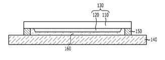
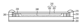
도 2는 본 발명의 일실시 예에 따른 엑스선 검출장치의 단면도,
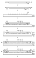
도 3은 본 발명에 따른 엑스선 검출장치의 제조 과정을 설명하기 위한 도면,
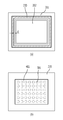
도 4는 테이프가 부착된 신틸레이터 패널의 평면도 및 실리콘 도트가 도포된 박막 트랜지스터 패널의 평면도이다.
210: 신틸레이터 패널 220: 박막 트랜지스터(TFT) 패널
230: 제1 댐부재 240: 경화성 물질층
250: 제2 댐부재 260: 제1 실링부재
270: 제2 실링부재 280: 서브글래스층
Claims (24)
- 기판과 상기 기판상에 형성된 형광층을 포함하여, 엑스선을 가시광으로 변환하는 신틸레이터 패널과, 상기 신틸레이터 패널에 의해 변환된 가시광의 세기에 따라 전기신호로 변환하는 광전 변환 소자를 포함하는 이미지 센서 패널을 포함하는 엑스선 검출장치에 있어서,
상기 신틸레이터 패널의 형광층 가장자리로부터 일정 간격 떨어져 일정 높이의 테두리 형태로 형성된 제1 댐부재;
상기 신틸레이터 패널의 형광층과 상기 이미지 센서 패널의 액티브 영역 사이의 상기 제1 댐부재 내측 공간에 충진되어 상기 신틸레이터 패널과 상기 이미지 센서 패널을 균일하게 접착하는 경화성 물질층;
상기 이미지 센서 패널의 가장자리에 형성된 제2 댐부재; 및
상기 제2 댐부재와 상기 제1 댐부재 사이의 공간에 충진되는 제1 실링부재
를 포함하는 엑스선 검출장치.
- 엑스선을 가시광으로 변환하는 신틸레이터 패널과, 상기 신틸레이터 패널에 의해 변환된 가시광을 전기신호로 변환하는 광전 변환 소자를 포함하는 이미지 센서 패널을 포함하는 엑스선 검출장치에 있어서,
상기 신틸레이터 패널의 형광층 가장자리 외측에 일정 높이의 테두리 형태로 형성된 제1 댐부재;
상기 신틸레이터 패널의 형광층과 상기 이미지 센서 패널의 액티브 영역 사이의 상기 제1 댐부재 내측 공간에 충진되어 상기 신틸레이터 패널과 상기 이미지 센서 패널을 균일하게 접착하는 경화성 물질층;
상기 이미지 센서 패널의 가장자리에 형성된 제2 댐부재; 및
상기 제2 댐부재와 상기 제1 댐부재 사이 공간에 충진된 제1 실링부재
를 포함하는 엑스선 검출장치.
- 제 1 항 또는 제 2 항에 있어서,
상기 경화성 물질층은 실리콘 층인 것을 특징으로 하는 엑스선 검출장치.
- 제 3 항에 있어서,
상기 실리콘 층은,
상기 이미지 센서 패널의 액티브 영역 상에 일정 간격으로 일정 도트량을 갖는 복수의 도트를 형성한 후, 상기 제1 댐부재가 형성된 상기 신틸레이터 패널을 상기 복수의 도트들이 형성된 상기 이미지 센서 패널 상에 압착하여 열 경화하는 것에 의해 형성되는 것을 특징으로 하는 엑스선 검출장치.
- 제 3 항에 있어서,
상기 제2 댐부재 상부와 상기 제1 실링부재 상부와 상기 신틸레이터 패널의 가장자리 상부에 도포되어 경화된 제2 실링부재를 더 포함하는 엑스선 검출장치.
- 제 3 항에 있어서,
상기 이미지 센서 패널은,
박막 트랜지스터(TFT) 패널을 포함하고, 상기 박막 트랜지스터 패널의 기저에 형성되어 상기 박막 트랜지스터 패널을 지지하는 서브글래스층을 더 포함하는 엑스선 검출장치.
- 제 4 항에 있어서,
상기 실리콘 층은 실리콘과 경화제를 일정 비율로 배합한 후 교반한 물질인 것을 특징으로 하는 엑스선 검출장치.
- 제 7 항에 있어서,
상기 실리콘 층은, 상기 실리콘과 상기 경화제를 10:1의 중량비로 배합하여 교반한 물질인 것을 특징으로 하는 엑스선 검출장치.
- 제 3 항에 있어서,
상기 제1 댐부재는, 접착 테이프인 것을 특징으로 하는 엑스선 검출장치.
- 제 9 항에 있어서,
상기 접착 테이프는 양면 아크릴 테이프인 것을 특징으로 하는 엑스선 검출장치.
- 제 3 항에 있어서,
상기 제2 댐부재는, 실리콘인 것을 특징으로 하는 엑스선 검출장치.
- 제 3 항에 있어서,
상기 제1 실링부재는, 에폭시인 것을 특징으로 하는 엑스선 검출장치.
- 제 5 항에 있어서,
상기 제2 실링부재는, 실리콘인 것을 특징으로 하는 엑스선 검출장치.
- 엑스선을 가시광으로 변환하는 신틸레이터 패널과, 상기 신틸레이터 패널에 의해 변환된 가시광을 전기신호로 변환하는 광전 변환 소자를 포함하는 이미지 센서 패널을 포함하는 엑스선 검출장치의 제조 방법에 있어서,
(a) 상기 신틸레이터 패널의 형광층 가장자리로부터 일정 간격 떨어져 일정 높이의 테두리 형태로 제1 댐부재를 형성하는 단계;
(b) 상기 신틸레이터 패널의 형광층과 상기 이미지 센서 패널의 액티브 영역 사이의 상기 제1 댐부재 내측 공간에 경화성 물질층을 형성하는 단계;
(c) 상기 이미지 센서 패널의 가장자리에 제2 댐부재를 형성하는 단계; 및
(d) 상기 신틸레이터 패널의 형광층을 실링하기 위해 상기 제2 댐부재와 상기 제1 댐부재 사이 공간에 제1 실링부재를 충진하는 단계
를 포함하는 엑스선 검출장치의 제조 방법.
- 제 14 항에 있어서,
상기 (b) 단계는,
상기 경화성 물질을 준비하는 단계;
상기 이미지 센서 패널의 액티브 영역 상에 일정 간격으로 일정 도트량을 갖는 상기 경화성 물질을 도포하는 단계;
상기 제1 댐부재가 형성된 상기 신틸레이터 패널을 상기 복수의 도트들이 도포된 상기 이미지 센서 패널 상에 압착하는 단계; 및
상기 신틸레이터 패널과 상기 이미지 센서 패널을 압착한 후 경화시키는 단계를 포함하는 엑스선 검출장치의 제조 방법.
- 제 15 항에 있어서,
상기 신틸레이터 패널과 상기 이미지 센서 패널을 압착한 후 경화시키는 단계는,
상기 신틸레이터 패널 상부에 일정 압력을 가한 후 일정 시간 동안 열을 가해 경화시키는 것을 특징으로 하는 엑스선 검출장치의 제조 방법.
- 제 14 항 또는 제 15 항에 있어서,
상기 제2 댐부재 상부와 상기 제1 실링부재 상부와 상기 신틸레이터 패널의 가장자리 상부에 제2 실링부재를 도포하여 경화시키는 단계를 더 포함하는 엑스선 검출장치의 제조 방법.
- 제 14 항에 있어서,
상기 경화성 물질을 준비하는 단계는,
실리콘과 경화제를 일정 비율로 배합하여 교반하는 것을 특징으로 하는 엑스선 검출장치의 제조 방법.
- 제 18 항에 있어서,
상기 경화성 물질을 준비하는 단계는,
상기 실리콘과 상기 경화제를 10:1의 중량비로 배합하여 교반하는 것을 특징으로 하는 엑스선 검출장치의 제조 방법.
- 제 14 항 또는 제 15 항에 있어서,
상기 제1 댐부재는, 접착 테이프인 것을 특징으로 하는 엑스선 검출장치의 제조 방법.
- 제 20 항에 있어서,
상기 접착 테이프는 양면 아크릴 테이프인 것을 특징으로 하는 엑스선 검출장치의 제조 방법.
- 제 14 항 또는 제 15 항에 있어서,
상기 (c) 단계는,
상기 이미지 센서 패널의 가장자리에 실리콘으로 일정 높이의 테두리를 형성한 후 경화시켜 상기 제2 댐부재를 형성하는 것을 특징으로 하는 엑스선 검출장치의 제조 방법.
- 제 14 항 또는 제 15 항에 있어서,
상기 (d) 단계는,
상기 제2 댐부재와 상기 제1 댐부재 사이에 에폭시로 충진하여 상기 제1 실링부재를 형성하는 것을 특징으로 하는 엑스선 검출장치의 제조 방법.
- 제 17 항에 있어서,
상기 제2 실링부재는, 실리콘인 것을 특징으로 하는 엑스선 검출장치의 제조 방법.
Applications Claiming Priority (2)
| Application Number | Priority Date | Filing Date | Title |
|---|---|---|---|
| KR1020090118143 | 2009-12-02 | ||
| KR20090118143 | 2009-12-02 |
Publications (1)
| Publication Number | Publication Date |
|---|---|
| KR20110063243A true KR20110063243A (ko) | 2011-06-10 |
Family
ID=44397257
Family Applications (1)
| Application Number | Title | Priority Date | Filing Date |
|---|---|---|---|
| KR1020100016143A Ceased KR20110063243A (ko) | 2009-12-02 | 2010-02-23 | 엑스선 검출장치 및 이의 제조방법 |
Country Status (1)
| Country | Link |
|---|---|
| KR (1) | KR20110063243A (ko) |
-
2010
- 2010-02-23 KR KR1020100016143A patent/KR20110063243A/ko not_active Ceased
Similar Documents
| Publication | Publication Date | Title |
|---|---|---|
| US7193218B2 (en) | Radiation detection device, method of producing the same, and radiation image pick-up system | |
| CN101689556B (zh) | 制造辐射探测器的方法 | |
| US6671347B2 (en) | Radiation imaging apparatus and radiation imaging system using the same | |
| US6414315B1 (en) | Radiation imaging with continuous polymer layer for scintillator | |
| US9366767B2 (en) | Radiation detecting apparatus and radiation detecting system | |
| KR101885016B1 (ko) | 방사선 검출기 및 그 제조방법 | |
| US9810791B2 (en) | Radiation detector and method for manufacturing the same | |
| CN105324683A (zh) | 具有嵌入在tft平板中的cmos传感器的x射线成像器 | |
| US9012859B2 (en) | Tiled X-ray imager panel and method of forming the same | |
| CN102621574A (zh) | 闪烁体面板、其制造方法和放射线检测设备 | |
| TW201506434A (zh) | 放射線檢測器及其製造方法 | |
| CN109324341A (zh) | 放射线检测装置及其制造方法和放射线成像系统 | |
| WO2016111093A1 (ja) | 放射線検出器及びその製造方法 | |
| CN105989906B (zh) | 放射线检测装置、放射线成像系统和制造方法 | |
| KR101202787B1 (ko) | 엑스선 검출장치 및 이의 제조방법 | |
| KR20120046127A (ko) | 엑스선 검출장치 및 이의 제조방법 | |
| KR20110063243A (ko) | 엑스선 검출장치 및 이의 제조방법 | |
| JP4380460B2 (ja) | 放射線検出装置、シンチレータパネル、及び放射線検出システム | |
| KR100964654B1 (ko) | 대면적 x선 검출장치 및 그의 제조방법 | |
| WO2010137384A1 (ja) | 放射線検出装置及びその製造方法 | |
| CN110707117A (zh) | 一种平板探测器 | |
| JP2002520577A (ja) | ベント型シーム付き広域x線イメージャおよび前記広域x先イメージャの作成方法 | |
| JP2011174830A (ja) | 放射線検出パネルおよび放射線画像検出器 | |
| JP4501238B2 (ja) | マルチスライス放射線検出器 | |
| JP2010091402A (ja) | 放射線検出装置の製造方法および放射線検出装置 |
Legal Events
| Date | Code | Title | Description |
|---|---|---|---|
| A201 | Request for examination | ||
| PA0109 | Patent application |
Patent event code: PA01091R01D Comment text: Patent Application Patent event date: 20100223 |
|
| PA0201 | Request for examination | ||
| E902 | Notification of reason for refusal | ||
| PE0902 | Notice of grounds for rejection |
Comment text: Notification of reason for refusal Patent event date: 20110509 Patent event code: PE09021S01D |
|
| PG1501 | Laying open of application | ||
| E601 | Decision to refuse application | ||
| PE0601 | Decision on rejection of patent |
Patent event date: 20111115 Comment text: Decision to Refuse Application Patent event code: PE06012S01D Patent event date: 20110509 Comment text: Notification of reason for refusal Patent event code: PE06011S01I |
|
| J201 | Request for trial against refusal decision | ||
| PJ0201 | Trial against decision of rejection |
Patent event date: 20111215 Comment text: Request for Trial against Decision on Refusal Patent event code: PJ02012R01D Patent event date: 20111115 Comment text: Decision to Refuse Application Patent event code: PJ02011S01I Appeal kind category: Appeal against decision to decline refusal Decision date: 20130123 Appeal identifier: 2011101009831 Request date: 20111215 |
|
| J801 | Dismissal of trial |
Free format text: REJECTION OF TRIAL FOR APPEAL AGAINST DECISION TO DECLINE REFUSAL REQUESTED 20111215 Effective date: 20130123 |
|
| PJ0801 | Rejection of trial |
Patent event date: 20130123 Patent event code: PJ08011S01D Comment text: Decision on Dismissal of Request for Trial (Dismissal of Decision) Decision date: 20130123 Appeal kind category: Appeal against decision to decline refusal Appeal identifier: 2011101009831 Request date: 20111215 |