KR20110063243A - X-ray detection device and manufacturing method thereof - Google Patents
X-ray detection device and manufacturing method thereof Download PDFInfo
- Publication number
- KR20110063243A KR20110063243A KR1020100016143A KR20100016143A KR20110063243A KR 20110063243 A KR20110063243 A KR 20110063243A KR 1020100016143 A KR1020100016143 A KR 1020100016143A KR 20100016143 A KR20100016143 A KR 20100016143A KR 20110063243 A KR20110063243 A KR 20110063243A
- Authority
- KR
- South Korea
- Prior art keywords
- panel
- scintillator panel
- dam member
- image sensor
- scintillator
- Prior art date
- Legal status (The legal status is an assumption and is not a legal conclusion. Google has not performed a legal analysis and makes no representation as to the accuracy of the status listed.)
- Ceased
Links
- 238000004519 manufacturing process Methods 0.000 title claims abstract description 20
- 238000001514 detection method Methods 0.000 title claims description 27
- 239000000463 material Substances 0.000 claims abstract description 78
- 238000007789 sealing Methods 0.000 claims abstract description 67
- 239000010409 thin film Substances 0.000 claims abstract description 63
- 229910052710 silicon Inorganic materials 0.000 claims abstract description 38
- 239000010703 silicon Substances 0.000 claims abstract description 38
- 239000004593 Epoxy Substances 0.000 claims abstract description 19
- NIXOWILDQLNWCW-UHFFFAOYSA-N acrylic acid group Chemical group C(C=C)(=O)O NIXOWILDQLNWCW-UHFFFAOYSA-N 0.000 claims abstract description 18
- 239000003795 chemical substances by application Substances 0.000 claims abstract description 15
- 239000000203 mixture Substances 0.000 claims abstract description 5
- 238000000034 method Methods 0.000 claims description 43
- XUIMIQQOPSSXEZ-UHFFFAOYSA-N Silicon Chemical group [Si] XUIMIQQOPSSXEZ-UHFFFAOYSA-N 0.000 claims description 37
- 238000001723 curing Methods 0.000 claims description 26
- 239000000758 substrate Substances 0.000 claims description 24
- 238000006243 chemical reaction Methods 0.000 claims description 15
- 238000003825 pressing Methods 0.000 claims description 7
- 238000011049 filling Methods 0.000 claims description 6
- 238000002156 mixing Methods 0.000 claims description 4
- 239000011521 glass Substances 0.000 claims description 3
- 238000003756 stirring Methods 0.000 claims description 2
- 239000002390 adhesive tape Substances 0.000 claims 4
- 239000011248 coating agent Substances 0.000 claims 1
- 238000000576 coating method Methods 0.000 claims 1
- 238000001029 thermal curing Methods 0.000 claims 1
- 239000010410 layer Substances 0.000 description 85
- KFZMGEQAYNKOFK-UHFFFAOYSA-N Isopropanol Chemical compound CC(C)O KFZMGEQAYNKOFK-UHFFFAOYSA-N 0.000 description 12
- 239000000853 adhesive Substances 0.000 description 10
- 230000001070 adhesive effect Effects 0.000 description 10
- XQPRBTXUXXVTKB-UHFFFAOYSA-M caesium iodide Chemical compound [I-].[Cs+] XQPRBTXUXXVTKB-UHFFFAOYSA-M 0.000 description 8
- 238000000151 deposition Methods 0.000 description 8
- 239000012790 adhesive layer Substances 0.000 description 5
- 230000008021 deposition Effects 0.000 description 5
- 230000008569 process Effects 0.000 description 5
- 230000008901 benefit Effects 0.000 description 4
- 239000010408 film Substances 0.000 description 4
- XAGFODPZIPBFFR-UHFFFAOYSA-N aluminium Chemical compound [Al] XAGFODPZIPBFFR-UHFFFAOYSA-N 0.000 description 3
- 229910052782 aluminium Inorganic materials 0.000 description 3
- 229920001187 thermosetting polymer Polymers 0.000 description 3
- OAICVXFJPJFONN-UHFFFAOYSA-N Phosphorus Chemical compound [P] OAICVXFJPJFONN-UHFFFAOYSA-N 0.000 description 2
- 230000015556 catabolic process Effects 0.000 description 2
- 239000013078 crystal Substances 0.000 description 2
- 230000002093 peripheral effect Effects 0.000 description 2
- 229920001296 polysiloxane Polymers 0.000 description 2
- 239000000126 substance Substances 0.000 description 2
- 238000002834 transmittance Methods 0.000 description 2
- OKTJSMMVPCPJKN-UHFFFAOYSA-N Carbon Chemical compound [C] OKTJSMMVPCPJKN-UHFFFAOYSA-N 0.000 description 1
- 229910052684 Cerium Inorganic materials 0.000 description 1
- 230000005856 abnormality Effects 0.000 description 1
- 230000015572 biosynthetic process Effects 0.000 description 1
- 229910052799 carbon Inorganic materials 0.000 description 1
- GWXLDORMOJMVQZ-UHFFFAOYSA-N cerium Chemical compound [Ce] GWXLDORMOJMVQZ-UHFFFAOYSA-N 0.000 description 1
- 230000008859 change Effects 0.000 description 1
- 238000004140 cleaning Methods 0.000 description 1
- 238000010276 construction Methods 0.000 description 1
- 230000003247 decreasing effect Effects 0.000 description 1
- 230000007547 defect Effects 0.000 description 1
- 238000005137 deposition process Methods 0.000 description 1
- 238000013007 heat curing Methods 0.000 description 1
- 238000007689 inspection Methods 0.000 description 1
- 238000005304 joining Methods 0.000 description 1
- 239000007788 liquid Substances 0.000 description 1
- 230000007257 malfunction Effects 0.000 description 1
- 239000011159 matrix material Substances 0.000 description 1
- 230000004048 modification Effects 0.000 description 1
- 238000012986 modification Methods 0.000 description 1
- 230000035515 penetration Effects 0.000 description 1
- 238000009832 plasma treatment Methods 0.000 description 1
- 230000005855 radiation Effects 0.000 description 1
- 239000011347 resin Substances 0.000 description 1
- 229920005989 resin Polymers 0.000 description 1
- 230000035945 sensitivity Effects 0.000 description 1
Images
Classifications
-
- H—ELECTRICITY
- H10—SEMICONDUCTOR DEVICES; ELECTRIC SOLID-STATE DEVICES NOT OTHERWISE PROVIDED FOR
- H10F—INORGANIC SEMICONDUCTOR DEVICES SENSITIVE TO INFRARED RADIATION, LIGHT, ELECTROMAGNETIC RADIATION OF SHORTER WAVELENGTH OR CORPUSCULAR RADIATION
- H10F30/00—Individual radiation-sensitive semiconductor devices in which radiation controls the flow of current through the devices, e.g. photodetectors
- H10F30/20—Individual radiation-sensitive semiconductor devices in which radiation controls the flow of current through the devices, e.g. photodetectors the devices having potential barriers, e.g. phototransistors
- H10F30/29—Individual radiation-sensitive semiconductor devices in which radiation controls the flow of current through the devices, e.g. photodetectors the devices having potential barriers, e.g. phototransistors the devices being sensitive to radiation having very short wavelengths, e.g. X-rays, gamma-rays or corpuscular radiation
-
- H—ELECTRICITY
- H10—SEMICONDUCTOR DEVICES; ELECTRIC SOLID-STATE DEVICES NOT OTHERWISE PROVIDED FOR
- H10F—INORGANIC SEMICONDUCTOR DEVICES SENSITIVE TO INFRARED RADIATION, LIGHT, ELECTROMAGNETIC RADIATION OF SHORTER WAVELENGTH OR CORPUSCULAR RADIATION
- H10F19/00—Integrated devices, or assemblies of multiple devices, comprising at least one photovoltaic cell covered by group H10F10/00, e.g. photovoltaic modules
- H10F19/80—Encapsulations or containers for integrated devices, or assemblies of multiple devices, having photovoltaic cells
-
- H—ELECTRICITY
- H10—SEMICONDUCTOR DEVICES; ELECTRIC SOLID-STATE DEVICES NOT OTHERWISE PROVIDED FOR
- H10F—INORGANIC SEMICONDUCTOR DEVICES SENSITIVE TO INFRARED RADIATION, LIGHT, ELECTROMAGNETIC RADIATION OF SHORTER WAVELENGTH OR CORPUSCULAR RADIATION
- H10F30/00—Individual radiation-sensitive semiconductor devices in which radiation controls the flow of current through the devices, e.g. photodetectors
- H10F30/301—Individual radiation-sensitive semiconductor devices in which radiation controls the flow of current through the devices, e.g. photodetectors the devices being sensitive to very short wavelength, e.g. being sensitive to X-rays, gamma-rays or corpuscular radiation
-
- H—ELECTRICITY
- H10—SEMICONDUCTOR DEVICES; ELECTRIC SOLID-STATE DEVICES NOT OTHERWISE PROVIDED FOR
- H10F—INORGANIC SEMICONDUCTOR DEVICES SENSITIVE TO INFRARED RADIATION, LIGHT, ELECTROMAGNETIC RADIATION OF SHORTER WAVELENGTH OR CORPUSCULAR RADIATION
- H10F39/00—Integrated devices, or assemblies of multiple devices, comprising at least one element covered by group H10F30/00, e.g. radiation detectors comprising photodiode arrays
- H10F39/10—Integrated devices
- H10F39/12—Image sensors
- H10F39/191—Photoconductor image sensors
- H10F39/195—X-ray, gamma-ray or corpuscular radiation imagers
-
- H—ELECTRICITY
- H10—SEMICONDUCTOR DEVICES; ELECTRIC SOLID-STATE DEVICES NOT OTHERWISE PROVIDED FOR
- H10F—INORGANIC SEMICONDUCTOR DEVICES SENSITIVE TO INFRARED RADIATION, LIGHT, ELECTROMAGNETIC RADIATION OF SHORTER WAVELENGTH OR CORPUSCULAR RADIATION
- H10F71/00—Manufacture or treatment of devices covered by this subclass
-
- Y—GENERAL TAGGING OF NEW TECHNOLOGICAL DEVELOPMENTS; GENERAL TAGGING OF CROSS-SECTIONAL TECHNOLOGIES SPANNING OVER SEVERAL SECTIONS OF THE IPC; TECHNICAL SUBJECTS COVERED BY FORMER USPC CROSS-REFERENCE ART COLLECTIONS [XRACs] AND DIGESTS
- Y02—TECHNOLOGIES OR APPLICATIONS FOR MITIGATION OR ADAPTATION AGAINST CLIMATE CHANGE
- Y02E—REDUCTION OF GREENHOUSE GAS [GHG] EMISSIONS, RELATED TO ENERGY GENERATION, TRANSMISSION OR DISTRIBUTION
- Y02E10/00—Energy generation through renewable energy sources
- Y02E10/50—Photovoltaic [PV] energy
Landscapes
- Measurement Of Radiation (AREA)
Abstract
본 발명은 신틸레이터 패널과 박막 트랜지스터(TFT) 패널을 균일하게 접합하면서, 박막 트랜지스터(TFT) 패널과 신틸레이터 패널의 접합부위의 외곽을 3중으로 실링하여 습기 등에 의해 신틸레이터가 손상되는 것을 방지할 수 있는 엑스선 검출장치 및 이의 제조 방법에 관한 것으로, 신틸레이터 패널의 형광층(202)과 박막 트랜지스터(TFT) 패널(220)의 액티브 영역 사이의 공간에 실리콘과 경화제를 일정 비율로 혼합한 경화성 물질을 일정 두께로 증착하여 경화성 물질층(240)을 형성하는데, 상기 경화성 물질층(240)의 가장자리에 턱이 만들어 지도록 함으로써, 상기 경화성 물질층(240)에 의해 신틸레이터 패널에 대한 1차 실링이 이루어지고, 상기 경화성 물질층(240) 형성시 경화성 물질이 외부로 누출되지 않도록 하기 위한 아크릴 테이프로 구성된 제1 댐부재(230)에 의해 신틸레이터 패널에 대한 2차 실링이 이루어지며, 에폭시를 이용한 제1 실링부재(260)에 의해 신틸레이터 패널에 대한 3차 실링이 이루어지도록 한다.The present invention uniformly bonds the scintillator panel and the thin film transistor (TFT) panel while triple-sealing the outer portion of the junction between the thin film transistor (TFT) panel and the scintillator panel to prevent the scintillator from being damaged by moisture or the like. The present invention relates to an X-ray detecting apparatus and a method of manufacturing the same, wherein the curable material is a mixture of silicon and a curing agent in a predetermined ratio in the space between the fluorescent layer 202 of the scintillator panel and the active region of the thin film transistor (TFT) panel 220. Is deposited to a predetermined thickness to form a curable material layer 240, by forming a tuck on the edge of the curable material layer 240, the first sealing to the scintillator panel by the curable material layer 240 is The first dam member made of an acrylic tape to prevent the curable material from leaking to the outside when the curable material layer 240 is formed ( Secondary sealing is performed on the scintillator panel by 230, and the third sealing on the scintillator panel is performed by the first sealing member 260 using epoxy.
Description
본 발명은 박막 트랜지스터(TFT: Thin Film Transistor) 패널 및 신틸레이터 패널의 접합 구조를 개선한 엑스선(X-ray) 검출장치 및 이의 제조방법에 관한 것으로, 더욱 자세하게는 신틸레이터 패널과 TFT 패널을 균일하게 접합하면서, TFT 패널과 신틸레이터 패널의 접합부위의 외곽을 3중으로 실링한 엑스선 검출장치 및 이의 제조방법에 관한 것이다.
The present invention relates to an X-ray (X-ray) detection device and a manufacturing method of the improved junction structure of a thin film transistor (TFT) panel and a scintillator panel, and more particularly, uniformly scintillator panel and TFT panel The present invention relates to an X-ray detecting apparatus and a method of manufacturing the same, which triple-sealed the outer portion of the bonding portion of the TFT panel and the scintillator panel while bonding them together.
필름을 이용한 아날로그 방식의 X선 검출장치는 이미지 형상화 작업에 시간이 걸리고 필름을 저장해야 하는 공간을 확보해야 하며, 필름 및 추가 인력에 대한 비용이 발생하는 단점이 있다. 이러한 이유로 최근에는 박막 트랜지스터(TFT) 또는 CCD 또는 CMOS와 같은 이미지 센서를 이용한 디지털 X선 검출장치가 널리 사용되고 있다.Analogue X-ray detection apparatus using a film takes a long time to image the image, must secure a space to store the film, there is a disadvantage that the cost for the film and additional manpower. For this reason, a digital X-ray detection apparatus using a thin film transistor (TFT) or an image sensor such as a CCD or a CMOS has been widely used in recent years.
디지털 X선 검출장치는 X선으로 촬영한 영상을 디지털 신호로 출력하는 장치로, 직접 방식과 간접 방식으로 크게 구분할 수 있다.The digital X-ray detecting apparatus is a device that outputs an image taken by X-ray as a digital signal, and can be divided into a direct method and an indirect method.
직접 방식은 아모포스 세륨(Se) 등의 광 도전막을 이용하여 X선을 전하로 직접 변환하는 방식이다. 이에 비해 간접 방식은 형광 패널(신틸레이터(scintillator) 패널이라고 함)이 X선을 가시광으로 변환하고, 변환된 가시광을 포토 다이오드 등의 광전 변환 소자에 의해 전하로 변환하는 방식이다.The direct method is a method of directly converting X-rays to electric charges using a photoconductive film such as amorphous cerium (Se). In contrast, the indirect method is a method in which a fluorescent panel (called a scintillator panel) converts X-rays into visible light and converts the converted visible light into electric charges by a photoelectric conversion element such as a photodiode.
직접 방식의 X선 검출장치는 해상도가 우수하다는 장점이 있지만, 고전압을 이용하기 때문에 절연 파괴의 문제가 발생할 수 있고, 이에 따라 신뢰성이 저하되는 단점이 있다. 또한 직접 방식의 엑스선 검출장치는 낮은 암전류 특성, 고감도 특성 및 열적 안정성 등을 구비한 광도전 재료를 쉽게 이용할 수 없다는 단점이 있다.Although the direct type X-ray detecting apparatus has an advantage of excellent resolution, a problem of dielectric breakdown may occur due to the use of a high voltage, and thus there is a disadvantage in that reliability is lowered. In addition, the direct X-ray detecting apparatus has a disadvantage in that it is not easy to use a photoconductive material having low dark current characteristics, high sensitivity characteristics, and thermal stability.
한편, 간접 방식의 X선 검출장치는 신호 전하를 발생시키기 위해 포토 다이오드 등을 이용하기 때문에 직접 방식과 같은 고전압을 이용하지 않아 절연 파괴의 문제는 없으며, 형광 물질이나 포토 다이오드와 같은 기술은 이미 상당한 수준에 도달되어 있기 때문에 제품화가 용이하다. 따라서 최근에는 간접 방식이 각광을 받고 있다.On the other hand, since the indirect X-ray detector uses a photodiode to generate signal charges, there is no problem of dielectric breakdown because it does not use a high voltage like the direct method. Since the level is reached, it is easy to commercialize. Therefore, indirect methods have been in the spotlight recently.
간접 방식의 X선 검출장치는 대면적 구현을 위해 통상 신틸레이터 패널과 박막 트랜지스터(TFT) 패널을 이용한다. 즉 통상의 디지털 X선 검출장치는 알루미늄 기판과 세슘아이오다이드(cesium iodide; CsI)와 같은 형광층으로 이루어져 엑스선을 가시광으로 변환하는 신틸레이터 패널과, 상기 신틸레이터 패널에 의해 변환된 가시광을 받아들여 가시광의 세기에 따른 전기신호를 출력하는 광전 변환 소자를 포함하는 박막 트랜지스터(TFT) 패널로 이루어진다. 신틸레이터(형광층)는 세슘아이오다이드(CsI) 형광 물질을 컬럼(column) 형태의 단결정으로 증착하여 형성한다.Indirect X-ray detection apparatus typically uses a scintillator panel and a thin film transistor (TFT) panel to realize a large area. In other words, the conventional digital X-ray detecting apparatus is composed of an aluminum substrate and a fluorescent layer such as cesium iodide (CsI), a scintillator panel for converting X-rays into visible light, and receiving the visible light converted by the scintillator panel. And a thin film transistor (TFT) panel including a photoelectric conversion element for outputting an electric signal according to the intensity of visible light. The scintillator (fluorescent layer) is formed by depositing cesium iodide (CsI) fluorescent material as a single crystal in the form of a column.
여기서 박막 트랜지스터(TFT)가 형성된 기판 상에 신틸레이터(형광층)를 직접 증착하는 경우에는 200℃ 이상의 온도에서 형광층 증착 공정이 진행되기 때문에, 박막 트랜지스터(TFT)가 형성된 기판의 불량을 초래할 수 있다. 따라서 간접 방식의 X선 검출장치는 박막 트랜지스터(TFT)가 형성된 기판과 신틸레이터 패널을 부착하는데, 이 부착 방법에 따라 X선 검출장치의 효율이 크게 차이가 나게 된다. 즉, 박막 트랜지스터(TFT) 기판과 신틸레이터 패널을 부착할 때, 이들 사이에 공기층이 생성되면 공기와 매질 사이의 굴절률 차이로 인하여 계면에서 반사가 발생하여 광전 변환 소자로 들어가는 광의 효율이 떨어지고, 국부적으로 공기층이 생성되면 엑스선 검출 장치의 균일도가 떨어지게 된다.In this case, when the scintillator (fluorescent layer) is directly deposited on the substrate on which the thin film transistor (TFT) is formed, the fluorescent layer deposition process is performed at a temperature of 200 ° C. or higher, which may cause a defect of the substrate on which the thin film transistor (TFT) is formed. have. Therefore, the indirect X-ray detecting apparatus attaches a substrate on which a thin film transistor (TFT) is formed and a scintillator panel, and the efficiency of the X-ray detecting apparatus varies greatly according to the attaching method. That is, when attaching a thin film transistor (TFT) substrate and a scintillator panel, if an air layer is generated between them, reflection occurs at the interface due to the difference in refractive index between the air and the medium, thereby decreasing the efficiency of light entering the photoelectric conversion element, As the air layer is generated, the uniformity of the X-ray detection apparatus is reduced.
이러한 공기층의 생성을 억제하기 위해 신틸레이터 패널과 TFT 패널 사이에 접착제를 도포하여 서로 접착하는 방법이 있다. 즉, TFT 패널을 액티브 영역이 상부를 향하도록 바닥에 두고 상부에 접착제를 도포하여 접착층을 형성한 후, 신틸레이터 패널을 접착하는 방식으로 박막 트랜지스터(TFT) 패널과 신틸레이터 패널을 부착하는 방법이 있다.In order to suppress the formation of such an air layer, there is a method of applying an adhesive between the scintillator panel and the TFT panel and adhering to each other. That is, a method of attaching a thin film transistor (TFT) panel and a scintillator panel in such a manner that the TFT panel is placed on the bottom with the active area facing upward and an adhesive is applied on the top to form an adhesive layer and then the scintillator panel is adhered have.
이와 같은 접착제를 이용해 신틸레이터 패널과 박막 트랜지스터(TFT) 패널을 접착하는 방법이 캐논(Canon)에 허여된 미국특허 7,355,184호(발명의 명칭: 방사선 검출장치 및 이의 제조 방법)에 제시되어 있다. 미국특허 7,355,184호에는 신틸레이터의 밀착 불량에 의한 벗겨짐을 방지하고 증착에 의해 균일하면서도 정밀도 높은 주상 형광층을 형성할 수 있도록 하기 위해, 지지 기판상에 배치되는 형광체 바탕층의 표면을 대기압 플라즈마 처리하고, 상기 형광체 바탕층 표면상에 형광층을 형성하여 신틸레이터 패널을 제작하며, 2차원으로 배치되는 광전 변환 소자를 가지는 TFT 패널과 상기 제작된 신틸레이터 패널을 접착제에 의해 서로 접착한다.A method for bonding a scintillator panel and a thin film transistor (TFT) panel using such an adhesive is disclosed in US Pat. No. 7,355,184 (name of the invention: a radiation detection device and a manufacturing method thereof) issued to Canon. US Pat. No. 7,355,184 discloses an atmospheric pressure plasma treatment of the surface of the phosphor base layer disposed on the support substrate to prevent peeling due to poor adhesion of the scintillator and to form a uniform and highly accurate columnar fluorescent layer by deposition. A fluorescent layer is formed on the surface of the phosphor base layer to produce a scintillator panel, and the TFT panel having the photoelectric conversion elements arranged in two dimensions and the produced scintillator panel are bonded to each other with an adhesive.
하지만 이와 같이 접착제를 이용하여 신틸레이터 패널과 박막 트랜지스터(TFT) 패널을 서로 접착하는 경우 접착시에 신틸레이터 패널과 박막 트랜지스터(TFT) 패널 사이의 거리를 균일하게 하여 접착하는 것이 쉽지 않은 문제점이 있다. 더욱이 접착제를 이용하여 접착하는 경우, 기포가 함유되지 않도록 하는 것은 매우 어려운 일이다. 또한, 대면적의 신틸레이터 패널과 박막 트랜지스터(TFT) 패널을 접착할 수 있는 제조 장치의 구성이 어려우며, 신틸레이터 패널의 크기가 크기 때문에 발생하는 수많은 공정상의 어려움이 존재하였다.However, when the scintillator panel and the thin film transistor (TFT) panel are bonded to each other using an adhesive as described above, it is difficult to uniformly bond the scintillator panel and the thin film transistor (TFT) panel at the time of bonding. . Furthermore, when bonding with an adhesive, it is very difficult to prevent bubbles from being contained. In addition, it is difficult to construct a manufacturing apparatus capable of bonding a large area scintillator panel and a thin film transistor (TFT) panel, and there are a number of process difficulties due to the large size of the scintillator panel.
이러한 어려움은 치아나 악궁 등의 이미지를 획득하는 구강용 엑스선 검출장치와 같은 소면적 X선 검출장치를 제조하는데에는 큰 문제가 되지 않지만, 흉부나 두부 및 경부 등과 같은 광범위한 부분의 이미지를 획득하는 대면적 X선 검출장치를 제조하는데에는 큰 문제로 작용하게 된다.This difficulty is not a big problem in the manufacture of small area X-ray detectors, such as oral X-ray detectors that acquire images of teeth, arches, etc. It becomes a big problem to manufacture an area X-ray detection apparatus.
이와 같은 문제를 극복하기 위해 본 출원인에 의해 출원된 대한민국 공개특허공보 2009-0090155호(발명의 명칭: 대면적 X선 검출장치 및 그의 제조방법)에는 저점성 경화성 물질을 이용한 접착 방법이 제시되어 있다.In order to overcome such a problem, Korean Patent Application Publication No. 2009-0090155 filed by the present applicant (name of the invention: a large-area X-ray detection apparatus and a manufacturing method thereof) has disclosed an adhesive method using a low viscosity curable material. .
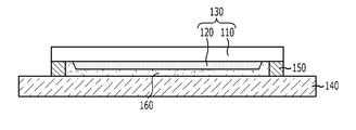
도 1은 본 출원인에 의해 출원된 종래의 대면적 X선 검출장치의 구조를 나타낸 단면도이다.1 is a cross-sectional view showing the structure of a conventional large-area X-ray detection device filed by the present applicant.
도 1을 참조하면, 가로 세로의 길이가 일정 크기를 갖는 박막 트랜지스터(TFT) 패널(140)에서 가시광을 센싱하는 광전 변환 소자가 배치되어 있지 않은 주변 영역에 점성도가 높은 제1 경화성 물질 또는 제1 자외선 경화성 물질로 댐(150)을 형성한다. 이와 같이 댐(150)을 형성한 다음, 상기 댐(150) 내측에 저점성의 제2 경화성 물질(예를 들어 액상 실리콘)을 도포하여 접착층(160)을 형성한다. 그리고 진공 챔버 내에 상기 접착층(160)이 위를 향하도록 TFT 패널을 위치시키고, 상기 접착층(160) 상부에 신틸레이터 패널(130)이 위치하도록 배치한 후, 진공 상태에서 신틸레이터 패널(130)과 박막 트랜지스터(TFT) 패널을 압착시킨다. 이렇게 신틸레이터 패널과 TFT 패널을 압착한 후, 댐(150)을 형성하는데 사용한 제1 열경화성 물질 또는 제1 자외선 경화성 물질과 접착층(160)을 형성하는데 사용한 제2 열경화성 물질 또는 제2 자외선 경화성 물질을 열 또는 자외선을 이용하여 경화시킨다.Referring to FIG. 1, a first curable material having a high viscosity or a first viscosity in a peripheral region where a photoelectric conversion element for sensing visible light is not disposed in a thin film transistor (TFT)
이와 같이 신틸레이터 패널과 TFT 패널을 열경화성 물질 또는 자외선 경화성 물질을 이용해 접착함으로써, TFT 패널과 신틸레이터 패널을 공기층 발생을 억제하면서 균일하게 접합할 수 있다.Thus, by bonding a scintillator panel and a TFT panel using a thermosetting material or an ultraviolet curable material, a TFT panel and a scintillator panel can be bonded uniformly, suppressing generation of an air layer.
하지만, 이와 같은 종래의 X선 검출장치는 댐과 경화성 물질만으로 신틸레이터 패널을 박막 트랜지스터(TFT) 패널에 접착하기 때문에 온도 및 습기 등의 조건에서 접착 부위의 안정성이 떨어져 습기 또는 이물질 등이 신틸레이터 패널과 박막 트랜지스터(TFT) 패널 사이에 침투할 가능성이 높다.However, such a conventional X-ray detection device adheres the scintillator panel to the thin film transistor (TFT) panel using only a dam and a curable material. It is highly likely to penetrate between panels and thin film transistor (TFT) panels.
한편. 신틸레이터 패널과 박막 트랜지스터(TFT) 패널을 접착제 등을 이용해 부착한 후, 신틸레이터 패널의 테두리에 실링제(예를 들어 수지)를 부가하여 신틸레이터 패널과 TFT 패널의 안정성을 향상시키는 방법이 있다. 다시 말해, TFT 패널에 접착제를 도포하고, 접착제에 의해 접착되지 않은 TFT 패널의 테두리 부위와 신틸레이터 패널의 테두리 부위 사이에 실링제를 부가하는 방법이 있다. 이에 따라 신틸레이터 패널과 박막 트랜지스터(TFT) 패널 사이에 수분 또는 이물질이 침투하는 것을 방지하였다.Meanwhile. After attaching the scintillator panel and the thin film transistor (TFT) panel with an adhesive or the like, a sealing agent (for example, a resin) is added to the edge of the scintillator panel to improve the stability of the scintillator panel and the TFT panel. . In other words, there is a method of applying an adhesive to a TFT panel and adding a sealing agent between the edge portion of the TFT panel and the edge portion of the scintillator panel which are not bonded by the adhesive. As a result, penetration of moisture or foreign matter between the scintillator panel and the thin film transistor (TFT) panel is prevented.
하지만, 고온 등의 환경에서 상기 실링제에 의한 밀봉이 해제되면서 수분 또는 이물질이 침투하는 현상이 발생되고, 이에 따라 센서가 오동작하거나 고장이 발생되는 등의 문제점이 해결되지 않았다.
However, when the sealing by the sealing agent is released in an environment such as a high temperature, moisture or foreign matter penetrates, and thus a problem such as a malfunction or failure of the sensor is not solved.
따라서 본 발명은 상기와 같은 종래 기술의 문제점을 해결하기 위해 제안된 것으로, 신틸레이터 패널과 박막 트랜지스터(TFT) 패널을 균일하게 접합하면서, 박막 트랜지스터(TFT) 패널과 신틸레이터 패널의 접합부위의 외곽을 3중으로 실링하여 습기 등에 의해 신틸레이터가 손상되는 것을 방지할 수 있는 엑스선 검출장치 및 이의 제조 방법을 제공하는데 그 목적이 있다.Therefore, the present invention has been proposed to solve the above problems of the prior art, and the outer portion of the junction between the thin film transistor (TFT) panel and the scintillator panel while uniformly bonding the scintillator panel and the thin film transistor (TFT) panel. It is an object of the present invention to provide an X-ray detection apparatus and a method of manufacturing the same that can be prevented from damaging the scintillator due to moisture by sealing the triple.
본 발명의 다른 목적 및 장점들은 하기의 설명에 의해서 이해될 수 있으며, 본 발명의 실시예에 의해 보다 분명하게 알게 될 것이다. 또한, 본 발명의 목적 및 장점들은 특허 청구 범위에 나타낸 수단 및 그 조합에 의해 실현될 수 있음을 쉽게 알 수 있을 것이다.Other objects and advantages of the present invention can be understood by the following description, and will be more clearly understood by the embodiments of the present invention. Also, it will be readily appreciated that the objects and advantages of the present invention may be realized by the means and combinations thereof indicated in the claims.
상기의 목적을 달성하기 위하여 본 발명에 따른 엑스레이 검출장치는, 기판과 상기 기판상에 형성된 형광층을 포함하여, 엑스선을 가시광으로 변환하는 신틸레이터 패널과, 상기 신틸레이터 패널에 의해 변환된 가시광의 세기에 따라 전기신호로 변환하는 광전 변환 소자를 포함하는 이미지 센서 패널을 포함하는 엑스선 검출장치에 있어서, 상기 신틸레이터 패널의 형광층 가장자리로부터 일정 간격 떨어져 일정 높이의 테두리 형태로 형성된 제1 댐부재; 상기 신틸레이터 패널의 형광층과 상기 이미지 센서 패널의 액티브 영역 사이의 상기 제1 댐부재 내측 공간에 충진되어 상기 신틸레이터 패널과 상기 이미지 센서 패널을 균일하게 접착하는 경화성 물질층; 상기 이미지 센서 패널의 가장자리에 형성된 제2 댐부재; 및 상기 제2 댐부재와 상기 제1 댐부재 사이의 공간에 충진되어 상기 신틸레이터 패널과 상기 이미지 센서 패널을 실링하는 제1 실링부재를 포함한다.In order to achieve the above object, an X-ray detecting apparatus according to the present invention includes a scintillator panel for converting X-rays into visible light, including a substrate and a fluorescent layer formed on the substrate, and a visible light converted by the scintillator panel. An X-ray detecting apparatus including an image sensor panel including a photoelectric conversion element that converts an electric signal according to an intensity, the X-ray detecting apparatus comprising: a first dam member having a predetermined height at a predetermined distance from an edge of a fluorescent layer of the scintillator panel; A layer of curable material filled in the inner space of the first dam member between the fluorescent layer of the scintillator panel and the active region of the image sensor panel to uniformly adhere the scintillator panel and the image sensor panel; A second dam member formed at an edge of the image sensor panel; And a first sealing member filled in a space between the second dam member and the first dam member to seal the scintillator panel and the image sensor panel.
또한, 본 발명에 따른 엑스선 검출장치는, 엑스선을 가시광으로 변환하는 신틸레이터 패널과, 상기 신틸레이터 패널에 의해 변환된 가시광을 전기신호로 변환하는 광전 변환 소자를 포함하는 이미지 센서 패널을 포함하는 엑스선 검출장치에 있어서, 상기 신틸레이터 패널의 형광층 가장자리 외측에 일정 높이의 테두리 형태로 형성된 제1 댐부재; 상기 신틸레이터 패널의 형광층과 상기 이미지 센서 패널의 액티브 영역 사이의 상기 제1 댐부재 내측 공간에 충진되어 상기 신틸레이터 패널과 상기 이미지 센서 패널을 균일하게 접착하는 경화성 물질층; 상기 이미지 센서 패널의 가장자리에 형성된 제2 댐부재; 및 상기 제2 댐부재와 상기 제1 댐부재 사이 공간에 충진되는 제1 실링부재를 포함한다.In addition, the X-ray detecting apparatus according to the present invention, the X-ray including a scintillator panel for converting the X-ray to visible light, and an image sensor panel including a photoelectric conversion element for converting the visible light converted by the scintillator panel into an electrical signal A detection apparatus comprising: a first dam member formed in an edge shape of a predetermined height outside an edge of a fluorescent layer of the scintillator panel; A layer of curable material filled in the inner space of the first dam member between the fluorescent layer of the scintillator panel and the active region of the image sensor panel to uniformly adhere the scintillator panel and the image sensor panel; A second dam member formed at an edge of the image sensor panel; And a first sealing member filled in a space between the second dam member and the first dam member.
바람직하게는 상기 경화성 물질층은 실리콘 층으로, 상기 실리콘 층은, 상기 이미지 센서 패널의 액티브 영역 상에 일정 간격으로 일정 도트량을 갖는 복수의 도트를 형성한 후, 상기 제1 댐부재가 형성된 상기 신틸레이터 패널을 상기 복수의 도트들이 형성된 상기 이미지 센서 패널 상에 압착하여 열 경화하는 것에 의해 형성된다.Preferably, the curable material layer is a silicon layer, and the silicon layer is formed on the active region of the image sensor panel at a predetermined interval with a plurality of dots having a predetermined dot amount, and the first dam member is formed. The scintillator panel is formed by pressing and thermally curing the image sensor panel on which the plurality of dots are formed.
바람직하게는 본 발명은 상기 제2 댐부재 상부와 상기 제1 실링부재 상부와 상기 신틸레이터 패널의 가장자리 상부에 도포되어 경화된 제2 실링부재를 더 포함한다.Preferably, the present invention further includes a second sealing member that is applied and cured on the upper portion of the second dam member, the upper portion of the first sealing member, and the edge of the scintillator panel.
바람직하게는 상기 이미지 센서 패널은, 박막 트랜지스터(TFT) 패널을 포함하고, 상기 박막 트랜지스터 패널의 기저에 형성되어 상기 박막 트랜지스터 패널을 지지하는 서브글래스층을 더 포함한다.Preferably, the image sensor panel further includes a thin film transistor (TFT) panel, and further includes a sub glass layer formed on the bottom of the thin film transistor panel to support the thin film transistor panel.
바람직하게는 상기 실리콘 층은 실리콘과 경화제를 10:1의 중량비로 배합하여 교반한 물질이다.Preferably, the silicon layer is a material in which silicon and a curing agent are mixed and mixed in a weight ratio of 10: 1.
바람직하게는 상기 제1 댐부재는, 양면 아크릴 테이프이고, 상기 제2 댐부재는 실리콘으로 구성되며, 상기 제1 실링부재는 에폭시로 구성되고, 상기 제2 실링부재는 실리콘으로 구성된다.Preferably, the first dam member is a double-sided acrylic tape, the second dam member is made of silicon, the first sealing member is made of epoxy, and the second sealing member is made of silicon.
또한 본 발명에 따른 엑스선 검출장치의 제조 방법은, 엑스선을 가시광으로 변환하는 신틸레이터 패널과, 상기 신틸레이터 패널에 의해 변환된 가시광을 전기신호로 변환하는 광전 변환 소자를 포함하는 이미지 센서 패널을 포함하는 엑스선 검출장치의 제조 방법에 있어서, (a) 상기 신틸레이터 패널의 형광층 가장자리로부터 일정 간격 떨어져 일정 높이의 테두리 형태로 제1 댐부재를 형성하는 단계; (b) 상기 신틸레이터 패널의 형광층과 상기 이미지 센서 패널의 액티브 영역 사이의 상기 제1 댐부재 내측 공간에 경화성 물질층을 형성하는 단계; (c) 상기 이미지 센서 패널의 가장자리에 제2 댐부재를 형성하는 단계; 및 (d) 상기 신틸레이터 패널의 형광층을 실링하기 위해 상기 제2 댐부재와 상기 제1 댐부재 사이 공간에 제1 실링부재를 충진하는 단계를 포함한다.In addition, the method of manufacturing an X-ray detecting apparatus according to the present invention includes an image sensor panel including a scintillator panel for converting X-rays into visible light and a photoelectric conversion element for converting visible light converted by the scintillator panel into an electrical signal. A method of manufacturing an X-ray detecting apparatus, the method comprising: (a) forming a first dam member in a shape of a rim having a predetermined height away from an edge of a fluorescent layer of the scintillator panel; (b) forming a layer of a curable material in an inner space of the first dam member between the fluorescent layer of the scintillator panel and the active region of the image sensor panel; (c) forming a second dam member on an edge of the image sensor panel; And (d) filling a first sealing member in a space between the second dam member and the first dam member to seal the fluorescent layer of the scintillator panel.
바람직하게는 상기 (b) 단계는, 상기 경화성 물질을 준비하는 단계; 상기 이미지 센서 패널의 액티브 영역 상에 일정 간격으로 일정 도트량을 갖는 상기 경화성 물질을 도포하는 단계; 상기 제1 댐부재가 형성된 상기 신틸레이터 패널을 상기 복수의 도트들이 도포된 상기 이미지 센서 패널 상에 압착하는 단계; 및 상기 신틸레이터 패널과 상기 이미지 센서 패널을 압착한 후 경화시키는 단계를 포함한다.Preferably step (b) comprises the steps of preparing the curable material; Applying the curable material having a predetermined dot amount at a predetermined interval on an active region of the image sensor panel; Pressing the scintillator panel on which the first dam member is formed on the image sensor panel to which the plurality of dots are applied; And hardening the scintillator panel and the image sensor panel after pressing them.
바람직하게는 상기 신틸레이터 패널과 상기 이미지 센서 패널을 압착한 후 경화시키는 단계는, 상기 신틸레이터 패널 상부에 일정 압력을 가한 후 일정 시간 동안 열을 가해 경화시키는 것을 포함한다.Preferably, the step of pressing and curing the scintillator panel and the image sensor panel includes applying a predetermined pressure to the scintillator panel and applying heat for a predetermined time to cure the scintillator panel and the image sensor panel.
바람직하게는 본 발명은 상기 제2 댐부재 상부와 상기 제1 실링부재 상부와 상기 신틸레이터 패널의 가장자리 상부에 제2 실링부재를 도포하여 경화시키는 단계를 더 포함한다.Preferably, the present invention further includes the step of applying and curing the second sealing member on the upper portion of the second dam member, the first sealing member, and the upper edge of the scintillator panel.
바람직하게는 상기 (c) 단계는, 상기 이미지 센서 패널의 가장자리에 실리콘으로 일정 높이의 테두리를 형성한 후 경화시켜 상기 제2 댐부재를 형성한다.Preferably, in the step (c), the edge of the image sensor panel is formed on the edge of silicon with a predetermined height and cured to form the second dam member.
바람직하게는 상기 (d) 단계는, 상기 제2 댐부재와 상기 제1 댐부재 사이에 에폭시로 충진하여 상기 제1 실링부재를 형성한다.
Preferably, in the step (d), the first sealing member is formed by filling with epoxy between the second dam member and the first dam member.
본 발명의 엑스선 검출장치에 따르면, 신틸레이터 패널과 박막 트랜지스터(TFT) 패널을 균일하게 접합하면서, 박막 트랜지스터(TFT) 패널과 신틸레이터 패널의 접합부위의 외곽을 3중으로 실링함으로써, 보다 안정된 실링 구조의 대면적 엑스선 검출장치가 가능하며, 보다 향상된 이미지 해상도를 갖는 엑스선 검출장치의 제조가 가능하다.
According to the X-ray detecting apparatus of the present invention, a more stable sealing structure is achieved by uniformly bonding the scintillator panel and the thin film transistor (TFT) panel while triple-sealing the outer portion of the junction between the thin film transistor (TFT) panel and the scintillator panel. A large area X-ray detection apparatus of the present invention is possible, and an X-ray detection apparatus having an improved image resolution is possible.
도 1은 종래의 신틸레이터 패널과 박막 트랜지스터(TFT) 패널의 접합 방식을 설명하기 위한 단면도,
도 2는 본 발명의 일실시 예에 따른 엑스선 검출장치의 단면도,
도 3은 본 발명에 따른 엑스선 검출장치의 제조 과정을 설명하기 위한 도면,
도 4는 테이프가 부착된 신틸레이터 패널의 평면도 및 실리콘 도트가 도포된 박막 트랜지스터 패널의 평면도이다.1 is a cross-sectional view illustrating a bonding method of a conventional scintillator panel and a thin film transistor (TFT) panel;
2 is a cross-sectional view of an X-ray detecting apparatus according to an embodiment of the present invention;
3 is a view for explaining a manufacturing process of the X-ray detecting apparatus according to the present invention,
4 is a plan view of a scintillator panel with a tape and a plan view of a thin film transistor panel with a silicon dot coated thereon.
상술한 목적, 특징 및 장점은 첨부된 도면과 관련한 다음의 상세한 설명을 통하여 보다 분명해 질 것이며, 그에 따라 본 발명이 속하는 기술분야에서 통상의 지식을 가진 자가 본 발명의 기술적 사상을 용이하게 실시할 수 있을 것이다. 또한, 본 발명을 설명함에 있어서 본 발명과 관련된 공지 기술에 대한 구체적인 설명이 본 발명의 요지를 불필요하게 흐릴 수 있다고 판단되는 경우에 그 상세한 설명을 생략하기로 한다.The foregoing and other objects, features and advantages of the present invention will become more apparent from the following detailed description of the present invention when taken in conjunction with the accompanying drawings, in which: There will be. In the following description, well-known functions or constructions are not described in detail since they would obscure the invention in unnecessary detail.
이하, 본 발명에 따른 엑스선 검출장치 및 이의 제조방법의 바람직한 실시 예를 첨부된 도면을 참조하여 상세히 설명한다.Hereinafter, with reference to the accompanying drawings, a preferred embodiment of the X-ray detecting apparatus and its manufacturing method according to the present invention will be described in detail.
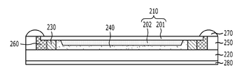
도 2는 본 발명의 일실시 예에 따른 박막 트랜지스터(TFT) 패널과 신틸레이터 패널의 접합 구조를 설명하기 위한 엑스선 검출장치의 단면도이다.2 is a cross-sectional view of an X-ray detecting apparatus for explaining a junction structure of a thin film transistor (TFT) panel and a scintillator panel according to an embodiment of the present invention.
본 발명에 따른 엑스선 검출장치는, 기판과 상기 기판상에 형성된 형광층을 포함하여 엑스선을 가시광으로 변환하는 신틸레이터 패널(210)과, 상기 신틸레이터 패널(210)에 의해 변환된 가시광의 세기에 따라 전기신호로 변환하는 광전 변환 소자를 포함하는 이미지 센서 패널(220)과, 상기 신틸레이터 패널의 형광층 가장자리로부터 일정 간격 떨어져 일정 높이를 갖는 테두리를 형성하여 경화성 물질이 외부로 유출되지 않도록 하는 제1 댐부재(230)와, 상기 신틸레이터 패널(210)의 형광층(202)와 상기 이미지 센서 패널(220)의 액티브 영역 사이의 상기 제1 댐부재(230) 내측 공간에 충진되어 상기 신틸레이터 패널(210)과 상기 이미지 센서 패널(220)을 균일하게 접착하는 경화성 물질층(240)과, 상기 이미지 센서 패널(220)의 가장자리에 형성된 제2 댐부재(250)와, 상기 제2 댐부재(250)와 상기 제1 댐부재(230) 사이의 공간에 충진되어 상기 신틸레이터 패널(210)을 실링하는 제1 실링부재(260)를 포함한다.The X-ray detecting apparatus according to the present invention includes a
또한 본 발명에 따른 엑스선 검출장치는 상기 제2 댐부재(250) 상부와 상기 제1 실링부재(260) 상부와 상기 신틸레이터 패널(210)의 상부 가장자리에 형성된 제2 실링부재(270)을 더 포함할 수 있다.In addition, the X-ray detecting apparatus according to the present invention further comprises a
이와 같은 구조를 갖는 본 발명에 따른 엑스선 검출장치의 구조를 도 2를 참조하여 보다 구체적으로 살펴본다.The structure of the X-ray detecting apparatus according to the present invention having such a structure will be described in more detail with reference to FIG. 2.
일반적으로 신틸레이터 패널(210)은 기판(201)과 고휘도 형광 물질인 요드화 세슘(CsI) 등을 퇴적시켜 성막하는 주상 결정구조의 형광층(또는 신틸레이터층 이라 함)(202)으로 구성된다. 여기서 기판은 알루미늄 기판 또는 카본 기판으로 구성될 수 있으며, 기판(201)의 다양한 물질에 대해서는 기 공지되어 있어 이에 대한 설명은 생략한다. 또한, 형광층 물질로 요드화 세슘(CsI)을 이용하는 것으로 설명하고 있지만, 이외에도 다양한 형광층 물질이 이용될 수 있음은 자명하다 할 것이다. 이와 같이 구성된 신틸레이터 패널(210)은 엑스선이 피검체를 투과하여 조사되면 기판(201)을 투과한 엑스선이 형광층(202)에 의해 가시광으로 변환되고, 광 반사 특성을 갖는 기판(201)에 의해 형광층(202)에 의해 변환된 가시광은 외부로 누설되지 않고 광전 변환 소자를 포함하는 박막 트랜지스터(TFT) 패널로 전달된다.In general, the
통상 이미지 센서 종류로는 CCD 이미지 센서, CMOS 이미지 센서, TFT 이미지 센서가 있지만, 본 발명의 실시 예에서는 대면적화에 유리한 TFT 이미지 센서를 예로 들어 설명한다. 하지만, 본 발명의 권리범위는 TFT 이미지 센서에 국한되지 않음은 당업자에 있어 자명하다 할 것이다.In general, image sensor types include a CCD image sensor, a CMOS image sensor, and a TFT image sensor. However, embodiments of the present invention will be described using a TFT image sensor that is advantageous for large area. However, it will be apparent to those skilled in the art that the scope of the present invention is not limited to the TFT image sensor.
박막 트랜지스터(TFT) 패널(220)은 직사각형 또는 정사각형의 평판 형상으로 표면에 이차원의 매트릭스상으로 복수 개의 픽셀이 배열되고, 각 픽셀마다 스위칭 소자로 TFT(Thin Film Transistor)와 포토 다이오드와 같은 광전 변환 소자가 형성되어 있다. 또한 박막 트랜지스터 패널(220)에는 Read-out 회로와 같은 주변회로들이 배열될 수 있다. 여기서 박막 트랜지스터(TFT) 패널(220)은 가로 세로의 크기가 각각 17인치인 정사각형으로 구성될 수 있다. 또한 가로 세로의 크기가 각각 17인치인 경우 박막 트랜지스터 패널(220)이 휘어질 수 있기 때문에 박막 트랜지스터(TFT) 패널(220)의 기저면에는 상기 박막 트랜지스터(TFT) 패널(220)을 지지하고 외부의 저항 소자들을 보호하기 위한 서브글래스층(280)이 존재할 수 있다.The
이와 같은 신틸레이터 패널(210)과 박막 트랜지스터(TFT) 패널(220)을 부착하는데 있어, 본 발명에서는 경화성 물질(바람직하게는 실리콘과 경화제를 일정 비율로 배합한 물질)을 이용한다.In attaching such a
이에 대해 살펴보면, 신틸레이터 패널(210)과 박막 트랜지스터(TFT) 패널(220)을 부착하기 위해, 먼저 신틸레이터 패널의 형광층(202) 증착면으로부터 일정 간격(바람직하게는 증착면 가장자리로부터 1~2㎜) 떨어진 위치에 사각형 형태의 테두리인 제1 댐부재(230)를 형성한다. 여기서 제1 댐부재(230)는 양면 아크릴 테이프로 구성될 수 있으나, 이에 한정되는 것은 아니며, 다른 물질을 이용하는 것도 가능하다.In this regard, in order to attach the
또한, 신틸레이터 패널의 형광층(202)의 가장자리로부터 일정 간격 떨어진 위치에 양면 아크릴 테이프를 부착하는 것으로 설명하고 있지만, 형광층 가장자리면이 경사진 경우에는 형광층에 바로 인접하여 양면 아크릴 테이프를 부착하는 것도 가능하다. 하지만, 바람직하게는 형광층의 가장자리와 미세하게 간격을 유지하여 양면 아크릴 테이프를 부착하는 것이 유리하다. 그 이유는 신틸레이터 패널과 박막 트랜지스터(TFT) 패널 사이의 공간에 충진된 경화성 물질층의 가장자리에 턱이 형성되도록 함으로써, 이 경화성 물질층이 1차 실링 기능을 수행하도록 하기 위함이다.In addition, although it demonstrates attaching a double-sided acrylic tape in the position spaced apart from the edge of the
그리고 신틸레이터 패널(210)과 박막 트랜지스터(TFT) 패널 사이에 충진되는 경화성 물질층(240)은 30~50㎛의 두께로 형성되기 때문에 제1 댐부재(230)의 높이는 신틸레이터 패널의 형광층(202)의 상면보다 30~50㎛ 정도 높도록 하여, 신틸레이터 패널과 박막 트랜지스터(TFT) 패널 사이에 공간이 확보되도록 하는 것이 바람직하다.In addition, since the
신틸레이터 패널(210)과 박막 트랜지스터(TFT) 패널(220)을 부착하기 위한 경화성 물질층(240)은 사각 테두리 형태로 형성된 제1 댐부재(230) 내의 상기 신틸레이터 패널(210)의 형광층(202)과 박막 트랜지스터 패널(210)의 액티브 영역 사이의 공간에 형성된다. 경화성 물질층(240)은 30~50㎛의 두께로 형성되는 것이 바람직하다. 경화성 물질층(240)의 두께가 너무 두꺼운 경우에는 가시광 투과율에 문제가 발생되기 때문에 경화성 물질층(240)의 두께는 가시광 투과율에 영향이 없도록 조절하는 것이 좋다.The
한편, 제1 댐부재(230)가 신틸레이터 패널의 형광층 증착면 가장자리로부터 일정 정도 떨어져 있기 때문에, 경화성 물질층(240)은 가장자리에 턱이 형성된 것과 같은 그릇 형상을 갖게 되고, 경화성 물질층(240)의 가장자리 턱이 신틸레이터 패널의 형광층의 증착면 외측에 형성되기 때문에 상기 경화성 물질층(240)의 가장자리 턱은 신틸레이터 패널을 1차 실링하는 기능을 갖게 된다.On the other hand, since the
이와 같은 경화성 물질층(240)은 실리콘과 경화제를 중량비로 10:1로 배합하여 형성한 물질을 이용할 수 있는데, 이에 한정되지는 않으며, 다양한 물질로 구성될 수 있음은 자명하다 할 것이다. 경화성 물질을 제1 댐부재(230) 내측에 충진하는 방법은 도 3 및 도 4를 참조하여 후술한다.The
제2 댐부재(250)는 신틸레이터 패널(210)과 박막 트랜지스터 패널(220)을 실링하기 위해 제1 실링부재(260)를 충진할 때, 제1 실링부재(260)가 외측으로 누출되는 것을 방지하기 위해 박막 트랜지스터(TFT) 패널(220)의 상부 가장자리에 일정 높이를 갖도록 사각형 테두리 형태로 형성된다. 상기 제2 댐부재(250)는 실리콘으로 형성될 수 있지만, 이에 한정되지는 않으며 다양한 물질로 형성될 수 있다.When the
제1 실링부재(260)는 제2 댐부재(250)와 제1 댐부재(230) 사이의 공간에 충진되어 신틸레이터 패널과 박막 트랜지스터(TFT) 패널을 실링하기 위한 것으로, 에폭시(Epoxy) 물질로 구성될 수 있다. 물론 제1 실링부재(260)로 에폭시가 아닌 실리콘 등을 사용하는 것도 가능하다. 따라서 제2 댐부재(250)는 신틸레이터 패널의 외곽 가이드 실링에서 제1 실링부재인 에폭시(Epoxy)가 외측으로 흐르지 않도록 한다.The
또한 본 발명의 일실시 예에서는 제2 댐부재(250) 상부와 제1 실링부재인 에폭시 층(260) 상부와 신틸레이터 패널의 기판(201) 상면 가장자리에 제2 실링부재(270)을 추가 형성하여 신틸레이터 패널의 실링을 보강할 수 있다. 여기서 제2 실링부재(270)는 실리콘일 수 있지만, 에폭시를 이용하는 것도 가능하다.In addition, in an embodiment of the present invention, a
이상에서 설명한 바와 같이 본 발명에 따른 대면적 엑스선 검출장치는, 신틸레이터 패널의 형광층(202)과 박막 트랜지스터(TFT) 패널(220)의 액티브 영역 사이의 공간에 실리콘과 경화제를 일정 비율로 혼합한 경화성 물질을 일정 두께로 증착하여 경화성 물질층(240)을 형성하는데, 상기 경화성 물질층(240)의 가장자리에 턱이 만들어 지도록 함으로써, 상기 경화성 물질층(240)에 의해 신틸레이터 패널에 대한 1차 실링이 이루어지고, 상기 경화성 물질층(240) 형성시 경화성 물질이 외부로 누출되지 않도록 하기 위한 아크릴 테이프로 구성된 제1 댐부재(230)에 의해 신틸레이터 패널에 대한 2차 실링이 이루어지며, 에폭시를 이용한 제1 실링부재(260)에 의해 신틸레이터 패널에 대한 3차 실링이 이루어지도록 한 것에 그 특징이 있다.As described above, the large-area X-ray detection apparatus according to the present invention mixes silicon and a curing agent in a predetermined ratio in the space between the
이하에서는 도 3 및 도 4를 참조하여 이와 같은 구조적 특징을 갖는 본 발명에 따른 대면적 엑스선 검출장치의 제조 방법을 설명한다.Hereinafter, a method of manufacturing a large area X-ray detecting apparatus according to the present invention having such a structural feature will be described with reference to FIGS. 3 and 4.
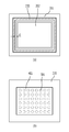
도 3은 본 발명에 따른 엑스선 검출장치의 제조 과정을 설명하기 위한 도면이고, 도 4는 아크릴 테이프가 부착된 신틸레이터 패널의 평면도 및 실리콘 도트가 도포된 박막 트랜지스터 패널의 평면도를 나타낸 것이다.3 is a view for explaining a manufacturing process of the X-ray detection apparatus according to the present invention, Figure 4 is a plan view of a scintillator panel with an acrylic tape and a plan view of a thin film transistor panel coated with silicon dots.
먼저, 도 3에서 (a)에 도시된 바와 같이 신틸레이터 패널이 준비되면, 신틸레이터 패널에 대한 세정을 통해 이물질을 제거한다.First, when the scintillator panel is prepared as shown in (a) of FIG. 3, foreign substances are removed by cleaning the scintillator panel.
그리고 도 3에서 (b)에 도시된 바와 같이 신틸레이터 패널의 형광층(202) 증착면 가장자리에서 일정 거리(바람직하게는 1~2㎜) 떨어지게 하여 사각형 테두리 형태로 양면 아크릴 테이프를 이용해 제1 댐부재(230)를 형성한다. 즉, 도 4의 (a)에 도시된 바와 같이, 신틸레이터 패널의 기판(201) 상에 증착된 형광층(202)의 가장자리로부터 거리 d만큼 떨어지도록 하여 양면 아크릴 테이프를 이용해 사각형 테두리 형태의 제1 댐부재(230)를 형성한다. 여기서, 제1 댐부재(230)의 높이를 신틸레이터 패널의 형광층(202) 상면보다 30~50㎛ 정도 높게 하여, 신틸레이터 패널의 형광층(202)과 박막 트랜지스터(TFT) 패널의 액티브 영역 사이에 경화성 물질층(240)이 충진될 수 있는 공간이 형성되도록 한다.As shown in (b) of FIG. 3, the first dam is formed by using a double-sided acrylic tape in the form of a rectangular border by separating a predetermined distance (preferably 1 to 2 mm) from the edge of the deposition surface of the
이와 같이 신틸레이터 패널(210)에 제1 댐부재(230)를 형성한 다음 신틸레이터 패널의 형광층이 하부를 향하도록 하여 인 라인(In-line) 설비 좌측에 로딩한다. 이때 로딩된 신틸레이터 패널의 알루미늄 기판을 이소프로필 알콜(IPA)로 세정하여 이물질을 제거한다.As such, after forming the
다음 박막 트랜지스터(TFT) 패널의 액티브(Active) 영역을 이소프로필 알콜(IPA)로 세정하여 이물질을 제거하고, 박막 트랜지스터(TFT) 패널을 인라인 설비 우측에 로딩한다.The active area of the TFT panel is then cleaned with isopropyl alcohol (IPA) to remove foreign material, and the TFT panel is loaded on the right side of the inline facility.
다음 신틸레이터 패널의 형광층(202)과 박막 트랜지스터(TFT) 패널의 액티브 영역 사이에 경화성 물질층(240)을 형성하기 위해, 실리콘(KJR-9010)과 경화제(C-9010)를 중량비로 10:1로 배합한다. 그리고 배합 후 교반기를 이용해 2000RPM에서 2분 정도 교반하며, 2000RPM에서 2분 정도 탈포한다. 즉, 배합 후 교반기 설정에 있어 교반을 2000RPM/2분, 탈포를 2000RPM/2분으로 설정한다.Next, in order to form the
이렇게 교반된 실리콘은 도트(Dot) 18G(게이지), 외곽 실링(Sealing)을 위한 20G(게이지)의 두 개의 바렐에 각각 담겨지고, 상기 바렐을 설비에 장착한 후 도트(Dot)량을 체크한다.The agitated silicon is contained in two barrels of dots 18G (gauge) and 20G (gauge) for outer sealing, and the amount of dots is checked after mounting the barrel in the facility. .
그런 다음 도 3에서 (c)에 도시된 바와 같이 박막 트랜지스터(TFT) 패널(220)의 액티브 영역 상에 일정 간격으로 실리콘 도트(301)를 형성한다. 이때 박막 트랜지스터(TFT) 패널(220)의 액티브 영역 가장자리는 외곽 실링용 20G 바렐을 이용해 다른 부분보다 큰 도트를 형성한다. 다시 말해, 도 4에서 (b)에 도시된 바와 같이 박막 트랜지스터(TFT) 패널의 액티브 영역(401) 상에 실리콘과 경화제를 일정 비율로 배합하여 교반한 실리콘을 액티브 영역의 가장자리는 20G 도트를 형성하고 가장자리를 제외한 부분은 18G 도트를 일정 간격으로 형성한다. 여기서 가장자리의 도트량을 많게 하는 이유는 제1 댐부재와 신틸레이터 패널의 형광층 가장자리 간에 일정 정도 떨어져 있어 다른 부분에 비해 공간이 크기 때문이다. 또한 도트량은 신틸레이터 패널과 박막 트랜지스터 패널을 양면 아크릴 테이프를 이용해 부착하였을 때, 양면 아크릴 테이프 내측의 신틸레이터 패널과 박막 트랜지스터 패널 사이의 공간 체적과 동일한 양이 될 수 있도록 미리 계산된다. 이에 따라 박막 트랜지스터(TFT) 패널의 액티브 영역에 도트를 형성한 후 양면 아크릴 테이프가 형성된 신틸레이터 패널을 박막 트랜지스터(TFT) 패널 상부에 위치시켜 압력을 가하는 경우 경화성 물질이 공극없이 완벽하게 아크릴 테이프 내측에 채워질 수 있다. 여기서 신틸레이터 패널과 액티브 영역에 도트가 형성된 박막 트랜지스터 패널을 접합하는 과정은 진공 챔버 내에서 진공 상태 하에서 수행된다. 이에 따라 경화성 물질층 내에 기포가 발생되지 않는다.Then, as illustrated in (c) of FIG. 3,
도 3에서 (d)에 도시된 바와 같이 신틸레이터 패널과 박막 트랜지스터(TFT) 패널을 본딩(Bonding)하는 과정이 완료되면 경화성 물질인 실리콘을 경화하기 전에 X-ray 장비를 이용하여 기포, 이물질, TFT 패널 특성 변화 등을 검사하여 양, 불 판정을 진행한다.As shown in (d) of FIG. 3, when the bonding process of the scintillator panel and the thin film transistor (TFT) panel is completed, bubbles, foreign matters, The TFT panel characteristic change is examined to determine whether it is good or bad.
검사 결과, 이상이 없으면 이제 경화성 물질인 실리콘에 대한 경화 처리를 수행하게 되는데, 먼저 실리콘으로 합착되어 있는 제품이 경화 시 문제가 발생하지 않도록 일정 무게의 중량물을 제작하여 엑스선 검출장치 상부에 안착한다. 여기서 중량물은 중량이 17~18kg이고 면적이 신틸레이터 패널의 면적과 거의 동일한 크기가 바람직하다. 그리고, 실리콘의 경화를 위해 온도 조건을 설정하는데, 25℃에서 100℃로 온도를 상승하는 구간이 60분, 100℃로 온도를 유지하는 구간이 180분, 100℃에서 25℃로 온도를 하강시키는 구간이 90분으로 설정한다.As a result of the inspection, if there is no abnormality, the curing process for the silicone, which is a curable material, is now performed. First, a weight of a certain weight is manufactured and placed on the X-ray detection apparatus so that a problem does not occur during curing of the product bonded with silicon. The weight is preferably 17-18 kg in weight and approximately the same size as that of the scintillator panel. Then, to set the temperature conditions for the curing of the silicone, the section to increase the temperature from 25 ℃ to 100 ℃ 60 minutes, the section to maintain the temperature at 100 ℃ 180 minutes, the temperature is lowered from 100 ℃ to 25 ℃ The interval is set to 90 minutes.
이와 같이 열 경화 공정이 완료되면, X-ray 장비를 이용해 다시 기포, 이물질, TFT 패널 특성 변화 등을 검사하여 양, 불 판정을 수행한다.When the heat curing process is completed as described above, X-ray equipment is used to inspect the bubbles, foreign matters, and changes in the TFT panel characteristics to determine whether they are good or bad.
검사 결과 이상이 없으면 최외곽 실링(Sealing)을 진행하는데, 최외곽 실링은 박막 트랜지스터(TFT) 패널과 신틸레이터 패널 사이에 에폭시를 사용하여 외부로부터 온도 및 습기에 의해 형광층 및 광전 변환 소자가 손상되는 것을 방지한다.If there is no problem, the outermost sealing is carried out. The outermost sealing uses an epoxy between the thin film transistor (TFT) panel and the scintillator panel to damage the fluorescent layer and the photoelectric conversion element due to temperature and moisture from the outside. Prevent it.
이와 같은 최외곽 실링 과정을 살펴보면, 도 3에서 (e)에 도시된 바와 같이 제2 댐부재(250)로 실리콘을 바렐에 담아 설비에 장착하여 박막 트랜지스터(TFT) 패널의 가장자리에 사각 테두리 형태로 제2 댐부재(250)를 형성한다. 제2 댐부재(250)는 제1 실링부재인 에폭시가 외측으로 누출되는 것을 방지하기 위한 사전 작업이다.Referring to the outermost sealing process, as shown in (e) of FIG. 3, the silicon is placed in the barrel by the
다음 도 3의 (f)에 도시된 바와 같이 제2 댐부재(250)인 실리콘을 경화한 후 에폭시를 바렐에 담아 설비에 장착하여 제2 댐부재(250)와 제1 댐부재(230) 사이의 공간에 제1 실링부재인 에폭시(260)를 도포한다. 그리고 에폭시 경화를 위해 제품 전면과 후면에 자외선(U/V)을 조사한다.Next, as shown in (f) of FIG. 3, after curing the silicon, which is the
본 발명의 일실시 예에서는 도 3의 (g)에 도시된 바와 같이 제1 실링부재인 에폭시 경화 후 제2 댐부재(250) 상부와 제1 실링부재인 에폭시(260) 상부와 신틸레이터 패널의 기판 상부 가장자리를 실리콘(270)으로 도포하여 추가 실링을 수행할 수 있다.In one embodiment of the present invention, as shown in Figure 3 (g) of the first sealing member after the epoxy curing of the
이상에서 설명한 바와 같이 본 발명은, 신틸레이터 패널의 형광층(202)과 박막 트랜지스터(TFT) 패널(220)의 액티브 영역 사이에 실리콘과 경화제를 일정 비율로 혼합한 경화성 물질을 일정 두께로 증착하여 경화성 물질층(240)을 형성하고, 상기 경화성 물질층(240)의 가장자리에 턱이 형성되도록 함으로써, 상기 경화성 물질층(240)에 의해 신틸레이터 패널과 박막 트랜지스터 패널에 대한 1차 실링이 이루어지고, 상기 경화성 물질층(240) 형성시 경화성 물질이 외부로 누출되지 않도록 하기 위한 아크릴 테이프로 구성된 제1 댐부재(230)에 의해 2차 실링이 이루어지며, 에폭시를 이용한 제1 실링부재(260)에 의해 3차 실링이 이루어지도록 함으로써, 신틸레이터 패널과 박막 트랜지스터 패널의 접합 시 기포가 발생되지 않으면서 균일하게 부착할 수 있음과 동시에 3중으로 실링하여 제품 안정성을 향상시킬 수 있다.As described above, in the present invention, a curable material in which silicon and a curing agent are mixed at a predetermined ratio is deposited between a
이상에서 설명한 본 발명은, 본 발명이 속하는 기술 분야에서 통상의 지식을 가진 자에게 있어 본 발명의 기술적 사상을 벗어나지 않는 범위 내에서 여러 가지 치환, 변형 및 변경이 가능하므로 전술한 실시예 및 첨부된 도면에 의해 한정되는 것이 아니다.
It will be apparent to those skilled in the art that various modifications and variations can be made in the present invention without departing from the spirit or scope of the invention. The present invention is not limited to the drawings.
201: 기판 202: 형광층
210: 신틸레이터 패널 220: 박막 트랜지스터(TFT) 패널
230: 제1 댐부재 240: 경화성 물질층
250: 제2 댐부재 260: 제1 실링부재
270: 제2 실링부재 280: 서브글래스층201: substrate 202: fluorescent layer
210: scintillator panel 220: thin film transistor (TFT) panel
230: first dam member 240: curable material layer
250: second dam member 260: first sealing member
270: second sealing member 280: sub glass layer
Claims (24)
상기 신틸레이터 패널의 형광층 가장자리로부터 일정 간격 떨어져 일정 높이의 테두리 형태로 형성된 제1 댐부재;
상기 신틸레이터 패널의 형광층과 상기 이미지 센서 패널의 액티브 영역 사이의 상기 제1 댐부재 내측 공간에 충진되어 상기 신틸레이터 패널과 상기 이미지 센서 패널을 균일하게 접착하는 경화성 물질층;
상기 이미지 센서 패널의 가장자리에 형성된 제2 댐부재; 및
상기 제2 댐부재와 상기 제1 댐부재 사이의 공간에 충진되는 제1 실링부재
를 포함하는 엑스선 검출장치.
An image sensor including a substrate and a fluorescent layer formed on the substrate, a scintillator panel for converting X-rays into visible light, and a photoelectric conversion element for converting the signal into an electrical signal according to the intensity of the visible light converted by the scintillator panel. An X-ray detecting apparatus including a panel,
A first dam member formed in an edge shape having a predetermined height away from an edge of the fluorescent layer of the scintillator panel;
A layer of curable material filled in the inner space of the first dam member between the fluorescent layer of the scintillator panel and the active region of the image sensor panel to uniformly adhere the scintillator panel and the image sensor panel;
A second dam member formed at an edge of the image sensor panel; And
A first sealing member filled in a space between the second dam member and the first dam member;
X-ray detection apparatus comprising a.
상기 신틸레이터 패널의 형광층 가장자리 외측에 일정 높이의 테두리 형태로 형성된 제1 댐부재;
상기 신틸레이터 패널의 형광층과 상기 이미지 센서 패널의 액티브 영역 사이의 상기 제1 댐부재 내측 공간에 충진되어 상기 신틸레이터 패널과 상기 이미지 센서 패널을 균일하게 접착하는 경화성 물질층;
상기 이미지 센서 패널의 가장자리에 형성된 제2 댐부재; 및
상기 제2 댐부재와 상기 제1 댐부재 사이 공간에 충진된 제1 실링부재
를 포함하는 엑스선 검출장치.
An X-ray detection apparatus comprising a scintillator panel for converting X-rays into visible light and an image sensor panel including a photoelectric conversion element for converting visible light converted by the scintillator panel into an electrical signal,
A first dam member formed in a border shape having a predetermined height outside the edge of the fluorescent layer of the scintillator panel;
A layer of curable material filled in the inner space of the first dam member between the fluorescent layer of the scintillator panel and the active region of the image sensor panel to uniformly adhere the scintillator panel and the image sensor panel;
A second dam member formed at an edge of the image sensor panel; And
A first sealing member filled in a space between the second dam member and the first dam member;
X-ray detection apparatus comprising a.
상기 경화성 물질층은 실리콘 층인 것을 특징으로 하는 엑스선 검출장치.
The method according to claim 1 or 2,
And the curable material layer is a silicon layer.
상기 실리콘 층은,
상기 이미지 센서 패널의 액티브 영역 상에 일정 간격으로 일정 도트량을 갖는 복수의 도트를 형성한 후, 상기 제1 댐부재가 형성된 상기 신틸레이터 패널을 상기 복수의 도트들이 형성된 상기 이미지 센서 패널 상에 압착하여 열 경화하는 것에 의해 형성되는 것을 특징으로 하는 엑스선 검출장치.
The method of claim 3, wherein
The silicon layer is,
After forming a plurality of dots having a certain dot amount at a predetermined interval on the active region of the image sensor panel, the scintillator panel formed with the first dam member is pressed onto the image sensor panel formed with the plurality of dots. X-ray detection apparatus, characterized in that formed by thermal curing.
상기 제2 댐부재 상부와 상기 제1 실링부재 상부와 상기 신틸레이터 패널의 가장자리 상부에 도포되어 경화된 제2 실링부재를 더 포함하는 엑스선 검출장치.
The method of claim 3, wherein
And a second sealing member applied and cured on the upper portion of the second dam member, the upper portion of the first sealing member, and the edge of the scintillator panel.
상기 이미지 센서 패널은,
박막 트랜지스터(TFT) 패널을 포함하고, 상기 박막 트랜지스터 패널의 기저에 형성되어 상기 박막 트랜지스터 패널을 지지하는 서브글래스층을 더 포함하는 엑스선 검출장치.
The method of claim 3, wherein
The image sensor panel,
And a sub glass layer formed on the bottom of the thin film transistor panel to support the thin film transistor panel.
상기 실리콘 층은 실리콘과 경화제를 일정 비율로 배합한 후 교반한 물질인 것을 특징으로 하는 엑스선 검출장치.
The method of claim 4, wherein
The silicon layer is an X-ray detection apparatus, characterized in that the mixture of silicon and a curing agent in a predetermined ratio and then stirred.
상기 실리콘 층은, 상기 실리콘과 상기 경화제를 10:1의 중량비로 배합하여 교반한 물질인 것을 특징으로 하는 엑스선 검출장치.
The method of claim 7, wherein
The silicon layer is an X-ray detection apparatus, characterized in that the mixture of the silicon and the curing agent in a weight ratio of 10: 1 and stirred.
상기 제1 댐부재는, 접착 테이프인 것을 특징으로 하는 엑스선 검출장치.
The method of claim 3, wherein
And said first dam member is an adhesive tape.
상기 접착 테이프는 양면 아크릴 테이프인 것을 특징으로 하는 엑스선 검출장치.
The method of claim 9,
The adhesive tape is a double-sided acrylic tape, X-ray detection apparatus characterized in that.
상기 제2 댐부재는, 실리콘인 것을 특징으로 하는 엑스선 검출장치.
The method of claim 3, wherein
And the second dam member is silicon.
상기 제1 실링부재는, 에폭시인 것을 특징으로 하는 엑스선 검출장치.
The method of claim 3, wherein
The first sealing member is an X-ray detecting apparatus, characterized in that the epoxy.
상기 제2 실링부재는, 실리콘인 것을 특징으로 하는 엑스선 검출장치.
The method of claim 5, wherein
And the second sealing member is silicon.
(a) 상기 신틸레이터 패널의 형광층 가장자리로부터 일정 간격 떨어져 일정 높이의 테두리 형태로 제1 댐부재를 형성하는 단계;
(b) 상기 신틸레이터 패널의 형광층과 상기 이미지 센서 패널의 액티브 영역 사이의 상기 제1 댐부재 내측 공간에 경화성 물질층을 형성하는 단계;
(c) 상기 이미지 센서 패널의 가장자리에 제2 댐부재를 형성하는 단계; 및
(d) 상기 신틸레이터 패널의 형광층을 실링하기 위해 상기 제2 댐부재와 상기 제1 댐부재 사이 공간에 제1 실링부재를 충진하는 단계
를 포함하는 엑스선 검출장치의 제조 방법.
A method of manufacturing an X-ray detection apparatus comprising a scintillator panel for converting X-rays into visible light and an image sensor panel including a photoelectric conversion element for converting visible light converted by the scintillator panel into an electrical signal,
(A) forming a first dam member in the form of a border of a predetermined height away from the edge of the fluorescent layer of the scintillator panel;
(b) forming a layer of a curable material in an inner space of the first dam member between the fluorescent layer of the scintillator panel and the active region of the image sensor panel;
(c) forming a second dam member on an edge of the image sensor panel; And
(d) filling a first sealing member in a space between the second dam member and the first dam member to seal the fluorescent layer of the scintillator panel;
Method of manufacturing an x-ray detecting apparatus comprising a.
상기 (b) 단계는,
상기 경화성 물질을 준비하는 단계;
상기 이미지 센서 패널의 액티브 영역 상에 일정 간격으로 일정 도트량을 갖는 상기 경화성 물질을 도포하는 단계;
상기 제1 댐부재가 형성된 상기 신틸레이터 패널을 상기 복수의 도트들이 도포된 상기 이미지 센서 패널 상에 압착하는 단계; 및
상기 신틸레이터 패널과 상기 이미지 센서 패널을 압착한 후 경화시키는 단계를 포함하는 엑스선 검출장치의 제조 방법.
The method of claim 14,
In step (b),
Preparing the curable material;
Applying the curable material having a predetermined dot amount at a predetermined interval on an active region of the image sensor panel;
Pressing the scintillator panel on which the first dam member is formed on the image sensor panel to which the plurality of dots are applied; And
And compressing the scintillator panel and the image sensor panel and curing the scintillator panel.
상기 신틸레이터 패널과 상기 이미지 센서 패널을 압착한 후 경화시키는 단계는,
상기 신틸레이터 패널 상부에 일정 압력을 가한 후 일정 시간 동안 열을 가해 경화시키는 것을 특징으로 하는 엑스선 검출장치의 제조 방법.
The method of claim 15,
Pressing and curing the scintillator panel and the image sensor panel may include:
And applying heat to the scintillator panel at a predetermined pressure and curing the scintillator panel for a predetermined time.
상기 제2 댐부재 상부와 상기 제1 실링부재 상부와 상기 신틸레이터 패널의 가장자리 상부에 제2 실링부재를 도포하여 경화시키는 단계를 더 포함하는 엑스선 검출장치의 제조 방법.
The method according to claim 14 or 15,
And coating and curing the second sealing member on the upper portion of the second dam member, on the upper portion of the first sealing member, and on the edge of the scintillator panel.
상기 경화성 물질을 준비하는 단계는,
실리콘과 경화제를 일정 비율로 배합하여 교반하는 것을 특징으로 하는 엑스선 검출장치의 제조 방법.
The method of claim 14,
Preparing the curable material,
A method for producing an X-ray detection apparatus, characterized in that a mixture of silicon and a curing agent in a predetermined ratio and stirred.
상기 경화성 물질을 준비하는 단계는,
상기 실리콘과 상기 경화제를 10:1의 중량비로 배합하여 교반하는 것을 특징으로 하는 엑스선 검출장치의 제조 방법.
The method of claim 18,
Preparing the curable material,
And mixing the silicon and the curing agent in a weight ratio of 10: 1 to stir.
상기 제1 댐부재는, 접착 테이프인 것을 특징으로 하는 엑스선 검출장치의 제조 방법.
The method according to claim 14 or 15,
And said first dam member is an adhesive tape.
상기 접착 테이프는 양면 아크릴 테이프인 것을 특징으로 하는 엑스선 검출장치의 제조 방법.
The method of claim 20,
And said adhesive tape is a double-sided acrylic tape.
상기 (c) 단계는,
상기 이미지 센서 패널의 가장자리에 실리콘으로 일정 높이의 테두리를 형성한 후 경화시켜 상기 제2 댐부재를 형성하는 것을 특징으로 하는 엑스선 검출장치의 제조 방법.
The method according to claim 14 or 15,
In step (c),
And forming a second dam member on the edge of the image sensor panel with silicon at a predetermined height and then curing the edge to form the second dam member.
상기 (d) 단계는,
상기 제2 댐부재와 상기 제1 댐부재 사이에 에폭시로 충진하여 상기 제1 실링부재를 형성하는 것을 특징으로 하는 엑스선 검출장치의 제조 방법.
The method according to claim 14 or 15,
In step (d),
And the first sealing member is formed by filling with epoxy between the second dam member and the first dam member.
상기 제2 실링부재는, 실리콘인 것을 특징으로 하는 엑스선 검출장치의 제조 방법.The method of claim 17,
The second sealing member is a manufacturing method of the X-ray detecting apparatus, characterized in that the silicon.
Applications Claiming Priority (2)
| Application Number | Priority Date | Filing Date | Title |
|---|---|---|---|
| KR1020090118143 | 2009-12-02 | ||
| KR20090118143 | 2009-12-02 |
Publications (1)
| Publication Number | Publication Date |
|---|---|
| KR20110063243A true KR20110063243A (en) | 2011-06-10 |
Family
ID=44397257
Family Applications (1)
| Application Number | Title | Priority Date | Filing Date |
|---|---|---|---|
| KR1020100016143A Ceased KR20110063243A (en) | 2009-12-02 | 2010-02-23 | X-ray detection device and manufacturing method thereof |
Country Status (1)
| Country | Link |
|---|---|
| KR (1) | KR20110063243A (en) |
-
2010
- 2010-02-23 KR KR1020100016143A patent/KR20110063243A/en not_active Ceased
Similar Documents
| Publication | Publication Date | Title |
|---|---|---|
| US7193218B2 (en) | Radiation detection device, method of producing the same, and radiation image pick-up system | |
| CN101689556B (en) | Method of producing a radiation detector | |
| US6671347B2 (en) | Radiation imaging apparatus and radiation imaging system using the same | |
| US6414315B1 (en) | Radiation imaging with continuous polymer layer for scintillator | |
| US9366767B2 (en) | Radiation detecting apparatus and radiation detecting system | |
| KR101885016B1 (en) | Radiation detector and method for manufacturing same | |
| US9810791B2 (en) | Radiation detector and method for manufacturing the same | |
| CN105324683A (en) | X-ray imager with CMOS sensor embedded in TFT flat panel | |
| US9012859B2 (en) | Tiled X-ray imager panel and method of forming the same | |
| CN102621574A (en) | Scintillator panel, method of manufacturing the same, and radiation detection apparatus | |
| TW201506434A (en) | Radiation detector and method of manufacturing same | |
| CN109324341A (en) | Radiation detecting apparatus and its manufacturing method and radiation imaging system | |
| WO2016111093A1 (en) | Radiation detector and manufacturing method therefor | |
| CN105989906B (en) | Radiation detecting apparatus, radiation imaging system and manufacture method | |
| KR101202787B1 (en) | X-ray detector and Method for the same | |
| KR20120046127A (en) | X-ray detector and method for the same | |
| KR20110063243A (en) | X-ray detection device and manufacturing method thereof | |
| JP4380460B2 (en) | Radiation detection apparatus, scintillator panel, and radiation detection system | |
| KR100964654B1 (en) | Large area X-ray detector and manufacturing method thereof | |
| WO2010137384A1 (en) | Radiation detection device and method of manufacturing this device | |
| CN110707117A (en) | a flat panel detector | |
| JP2002520577A (en) | Wide area X-ray imager with vented seam and method of making said wide area X-point imager | |
| JP2011174830A (en) | Radiation detection panel and radiation image detector | |
| JP4501238B2 (en) | Multi-slice radiation detector | |
| JP2010091402A (en) | Method for manufacturing radiation detector and radiation detector |
Legal Events
| Date | Code | Title | Description |
|---|---|---|---|
| A201 | Request for examination | ||
| PA0109 | Patent application |
Patent event code: PA01091R01D Comment text: Patent Application Patent event date: 20100223 |
|
| PA0201 | Request for examination | ||
| E902 | Notification of reason for refusal | ||
| PE0902 | Notice of grounds for rejection |
Comment text: Notification of reason for refusal Patent event date: 20110509 Patent event code: PE09021S01D |
|
| PG1501 | Laying open of application | ||
| E601 | Decision to refuse application | ||
| PE0601 | Decision on rejection of patent |
Patent event date: 20111115 Comment text: Decision to Refuse Application Patent event code: PE06012S01D Patent event date: 20110509 Comment text: Notification of reason for refusal Patent event code: PE06011S01I |
|
| J201 | Request for trial against refusal decision | ||
| PJ0201 | Trial against decision of rejection |
Patent event date: 20111215 Comment text: Request for Trial against Decision on Refusal Patent event code: PJ02012R01D Patent event date: 20111115 Comment text: Decision to Refuse Application Patent event code: PJ02011S01I Appeal kind category: Appeal against decision to decline refusal Decision date: 20130123 Appeal identifier: 2011101009831 Request date: 20111215 |
|
| J801 | Dismissal of trial |
Free format text: REJECTION OF TRIAL FOR APPEAL AGAINST DECISION TO DECLINE REFUSAL REQUESTED 20111215 Effective date: 20130123 |
|
| PJ0801 | Rejection of trial |
Patent event date: 20130123 Patent event code: PJ08011S01D Comment text: Decision on Dismissal of Request for Trial (Dismissal of Decision) Decision date: 20130123 Appeal kind category: Appeal against decision to decline refusal Appeal identifier: 2011101009831 Request date: 20111215 |