KR20110005771A - Spectral module - Google Patents
Spectral module Download PDFInfo
- Publication number
- KR20110005771A KR20110005771A KR1020107015306A KR20107015306A KR20110005771A KR 20110005771 A KR20110005771 A KR 20110005771A KR 1020107015306 A KR1020107015306 A KR 1020107015306A KR 20107015306 A KR20107015306 A KR 20107015306A KR 20110005771 A KR20110005771 A KR 20110005771A
- Authority
- KR
- South Korea
- Prior art keywords
- light
- substrate
- spectroscopic
- fitting
- light transmitting
- Prior art date
Links
- 230000003595 spectral effect Effects 0.000 title description 34
- 239000000758 substrate Substances 0.000 claims abstract description 148
- 238000004611 spectroscopical analysis Methods 0.000 claims abstract description 14
- 239000011347 resin Substances 0.000 claims description 58
- 229920005989 resin Polymers 0.000 claims description 58
- 230000003287 optical effect Effects 0.000 claims description 36
- 238000000926 separation method Methods 0.000 claims description 13
- 239000003795 chemical substances by application Substances 0.000 claims description 11
- 238000000034 method Methods 0.000 claims 5
- 239000010410 layer Substances 0.000 description 46
- 238000005530 etching Methods 0.000 description 7
- 239000010931 gold Substances 0.000 description 6
- 229910052737 gold Inorganic materials 0.000 description 5
- 229910052782 aluminium Inorganic materials 0.000 description 4
- 230000005540 biological transmission Effects 0.000 description 4
- 238000000151 deposition Methods 0.000 description 4
- 238000004519 manufacturing process Methods 0.000 description 4
- 239000000463 material Substances 0.000 description 4
- 238000001514 detection method Methods 0.000 description 3
- 239000011521 glass Substances 0.000 description 3
- 230000031700 light absorption Effects 0.000 description 3
- 229910052751 metal Inorganic materials 0.000 description 3
- 239000002184 metal Substances 0.000 description 3
- 238000002161 passivation Methods 0.000 description 3
- 238000000206 photolithography Methods 0.000 description 3
- 229910018885 Pt—Au Inorganic materials 0.000 description 2
- 230000008021 deposition Effects 0.000 description 2
- 238000010586 diagram Methods 0.000 description 2
- 230000001678 irradiating effect Effects 0.000 description 2
- 238000002844 melting Methods 0.000 description 2
- 229910044991 metal oxide Inorganic materials 0.000 description 2
- 150000004706 metal oxides Chemical class 0.000 description 2
- 239000012466 permeate Substances 0.000 description 2
- 239000004033 plastic Substances 0.000 description 2
- 229920003023 plastic Polymers 0.000 description 2
- 239000002356 single layer Substances 0.000 description 2
- RZVAJINKPMORJF-UHFFFAOYSA-N Acetaminophen Chemical compound CC(=O)NC1=CC=C(O)C=C1 RZVAJINKPMORJF-UHFFFAOYSA-N 0.000 description 1
- 239000004925 Acrylic resin Substances 0.000 description 1
- 229920000178 Acrylic resin Polymers 0.000 description 1
- OKTJSMMVPCPJKN-UHFFFAOYSA-N Carbon Chemical compound [C] OKTJSMMVPCPJKN-UHFFFAOYSA-N 0.000 description 1
- 239000004593 Epoxy Substances 0.000 description 1
- JOYRKODLDBILNP-UHFFFAOYSA-N Ethyl urethane Chemical compound CCOC(N)=O JOYRKODLDBILNP-UHFFFAOYSA-N 0.000 description 1
- 239000004642 Polyimide Substances 0.000 description 1
- NIXOWILDQLNWCW-UHFFFAOYSA-N acrylic acid group Chemical group C(C=C)(=O)O NIXOWILDQLNWCW-UHFFFAOYSA-N 0.000 description 1
- XAGFODPZIPBFFR-UHFFFAOYSA-N aluminium Chemical group [Al] XAGFODPZIPBFFR-UHFFFAOYSA-N 0.000 description 1
- 229910052799 carbon Inorganic materials 0.000 description 1
- 239000000919 ceramic Substances 0.000 description 1
- 239000000805 composite resin Substances 0.000 description 1
- 238000001723 curing Methods 0.000 description 1
- 238000005520 cutting process Methods 0.000 description 1
- 238000009826 distribution Methods 0.000 description 1
- 230000000694 effects Effects 0.000 description 1
- 239000003822 epoxy resin Substances 0.000 description 1
- 239000000945 filler Substances 0.000 description 1
- 239000006260 foam Substances 0.000 description 1
- PCHJSUWPFVWCPO-UHFFFAOYSA-N gold Chemical compound [Au] PCHJSUWPFVWCPO-UHFFFAOYSA-N 0.000 description 1
- 238000013007 heat curing Methods 0.000 description 1
- 238000010438 heat treatment Methods 0.000 description 1
- 230000008018 melting Effects 0.000 description 1
- 239000007769 metal material Substances 0.000 description 1
- 230000000149 penetrating effect Effects 0.000 description 1
- 238000000016 photochemical curing Methods 0.000 description 1
- 229920000647 polyepoxide Polymers 0.000 description 1
- 229920001721 polyimide Polymers 0.000 description 1
- 230000002265 prevention Effects 0.000 description 1
- 230000002035 prolonged effect Effects 0.000 description 1
- 239000005297 pyrex Substances 0.000 description 1
- 238000000820 replica moulding Methods 0.000 description 1
- 229910052710 silicon Inorganic materials 0.000 description 1
- 239000010703 silicon Substances 0.000 description 1
- 238000001228 spectrum Methods 0.000 description 1
- -1 such as a resistor Substances 0.000 description 1
Images


Classifications
-
- G—PHYSICS
- G01—MEASURING; TESTING
- G01J—MEASUREMENT OF INTENSITY, VELOCITY, SPECTRAL CONTENT, POLARISATION, PHASE OR PULSE CHARACTERISTICS OF INFRARED, VISIBLE OR ULTRAVIOLET LIGHT; COLORIMETRY; RADIATION PYROMETRY
- G01J3/00—Spectrometry; Spectrophotometry; Monochromators; Measuring colours
- G01J3/02—Details
- G01J3/0205—Optical elements not provided otherwise, e.g. optical manifolds, diffusers, windows
- G01J3/0208—Optical elements not provided otherwise, e.g. optical manifolds, diffusers, windows using focussing or collimating elements, e.g. lenses or mirrors; performing aberration correction
-
- G—PHYSICS
- G01—MEASURING; TESTING
- G01J—MEASUREMENT OF INTENSITY, VELOCITY, SPECTRAL CONTENT, POLARISATION, PHASE OR PULSE CHARACTERISTICS OF INFRARED, VISIBLE OR ULTRAVIOLET LIGHT; COLORIMETRY; RADIATION PYROMETRY
- G01J3/00—Spectrometry; Spectrophotometry; Monochromators; Measuring colours
- G01J3/02—Details
- G01J3/0205—Optical elements not provided otherwise, e.g. optical manifolds, diffusers, windows
- G01J3/0243—Optical elements not provided otherwise, e.g. optical manifolds, diffusers, windows having a through-hole enabling the optical element to fulfil an additional optical function, e.g. a mirror or grating having a throughhole for a light collecting or light injecting optical fiber
-
- G—PHYSICS
- G01—MEASURING; TESTING
- G01J—MEASUREMENT OF INTENSITY, VELOCITY, SPECTRAL CONTENT, POLARISATION, PHASE OR PULSE CHARACTERISTICS OF INFRARED, VISIBLE OR ULTRAVIOLET LIGHT; COLORIMETRY; RADIATION PYROMETRY
- G01J3/00—Spectrometry; Spectrophotometry; Monochromators; Measuring colours
- G01J3/02—Details
- G01J3/0256—Compact construction
- G01J3/0259—Monolithic
-
- G—PHYSICS
- G01—MEASURING; TESTING
- G01J—MEASUREMENT OF INTENSITY, VELOCITY, SPECTRAL CONTENT, POLARISATION, PHASE OR PULSE CHARACTERISTICS OF INFRARED, VISIBLE OR ULTRAVIOLET LIGHT; COLORIMETRY; RADIATION PYROMETRY
- G01J3/00—Spectrometry; Spectrophotometry; Monochromators; Measuring colours
- G01J3/02—Details
- G01J3/0286—Constructional arrangements for compensating for fluctuations caused by temperature, humidity or pressure, or using cooling or temperature stabilization of parts of the device; Controlling the atmosphere inside a spectrometer, e.g. vacuum
-
- G—PHYSICS
- G01—MEASURING; TESTING
- G01J—MEASUREMENT OF INTENSITY, VELOCITY, SPECTRAL CONTENT, POLARISATION, PHASE OR PULSE CHARACTERISTICS OF INFRARED, VISIBLE OR ULTRAVIOLET LIGHT; COLORIMETRY; RADIATION PYROMETRY
- G01J3/00—Spectrometry; Spectrophotometry; Monochromators; Measuring colours
- G01J3/02—Details
- G01J3/0297—Constructional arrangements for removing other types of optical noise or for performing calibration
-
- G—PHYSICS
- G02—OPTICS
- G02B—OPTICAL ELEMENTS, SYSTEMS OR APPARATUS
- G02B27/00—Optical systems or apparatus not provided for by any of the groups G02B1/00 - G02B26/00, G02B30/00
- G02B27/42—Diffraction optics, i.e. systems including a diffractive element being designed for providing a diffractive effect
- G02B27/4233—Diffraction optics, i.e. systems including a diffractive element being designed for providing a diffractive effect having a diffractive element [DOE] contributing to a non-imaging application
- G02B27/4244—Diffraction optics, i.e. systems including a diffractive element being designed for providing a diffractive effect having a diffractive element [DOE] contributing to a non-imaging application in wavelength selecting devices
-
- G—PHYSICS
- G02—OPTICS
- G02B—OPTICAL ELEMENTS, SYSTEMS OR APPARATUS
- G02B5/00—Optical elements other than lenses
- G02B5/18—Diffraction gratings
- G02B5/1814—Diffraction gratings structurally combined with one or more further optical elements, e.g. lenses, mirrors, prisms or other diffraction gratings
-
- G—PHYSICS
- G02—OPTICS
- G02B—OPTICAL ELEMENTS, SYSTEMS OR APPARATUS
- G02B5/00—Optical elements other than lenses
- G02B5/18—Diffraction gratings
- G02B5/1847—Manufacturing methods
- G02B5/1852—Manufacturing methods using mechanical means, e.g. ruling with diamond tool, moulding
-
- G—PHYSICS
- G02—OPTICS
- G02B—OPTICAL ELEMENTS, SYSTEMS OR APPARATUS
- G02B5/00—Optical elements other than lenses
- G02B5/18—Diffraction gratings
- G02B5/1861—Reflection gratings characterised by their structure, e.g. step profile, contours of substrate or grooves, pitch variations, materials
-
- G—PHYSICS
- G02—OPTICS
- G02B—OPTICAL ELEMENTS, SYSTEMS OR APPARATUS
- G02B7/00—Mountings, adjusting means, or light-tight connections, for optical elements
- G02B7/02—Mountings, adjusting means, or light-tight connections, for optical elements for lenses
- G02B7/025—Mountings, adjusting means, or light-tight connections, for optical elements for lenses using glue
-
- G—PHYSICS
- G01—MEASURING; TESTING
- G01J—MEASUREMENT OF INTENSITY, VELOCITY, SPECTRAL CONTENT, POLARISATION, PHASE OR PULSE CHARACTERISTICS OF INFRARED, VISIBLE OR ULTRAVIOLET LIGHT; COLORIMETRY; RADIATION PYROMETRY
- G01J3/00—Spectrometry; Spectrophotometry; Monochromators; Measuring colours
- G01J3/12—Generating the spectrum; Monochromators
- G01J2003/1213—Filters in general, e.g. dichroic, band
Abstract
분광모듈(1)은, 전면(2a)으로부터 입사한 광(L1)을 투과시키는 기판(2)과 기판(2)에 입사한 광(L1)을 투과시키는 렌즈부(3)와 렌즈부(3)에 입사한 광(L1)을 분광하고, 아울러, 반사하는 분광부(4)와, 분광부(4)에 의해서 반사된 광(L2)을 검출하는 광검출소자(5)를 구비하고 있다. 기판(2)에는, 광검출소자(5)를 위치결정하기 위한 기준부가 되는 얼라이먼트 마크(12a, 12b) 등에 대해서 소정의 위치관계를 가지는 오목부(19)가 형성되어 있고, 렌즈부(3)는 오목부(19)에 끼워맞춰져 있다. 분광모듈(1)에 의하면, 렌즈부(3)를 오목부(19)에 끼워맞춰지게 하는 것만으로, 분광부(4)로 광검출소자(5)와의 패시브(passive) 얼라이먼트가 실현된다.The spectroscopic module 1 includes a substrate 2 for transmitting the light L1 incident from the front surface 2a and a lens part 3 and a lens part 3 for transmitting the light L1 incident on the substrate 2. And a light detecting element 5 for spectroscopy the light L1 incident on the light beam) and reflects the light L2 reflected by the spectroscopic part 4. The substrate 2 is formed with a recess 19 having a predetermined positional relationship with respect to the alignment marks 12a and 12b serving as a reference for positioning the photodetector 5, and the lens portion 3 is It fits in the recessed part 19. According to the spectroscopic module 1, the passive alignment with the photodetecting element 5 is realized by the spectroscopic section 4 only by fitting the lens section 3 to the concave section 19.

Description
본 발명은 광을 분광(分光)하여 검출하는 분광모듈에 관한 것이다.The present invention relates to a spectroscopic module for spectroscopically detecting light.
종래의 분광모듈로서, 예를 들면 특허문헌 1 ~ 3에 기재된 것이 알려져 있다. 특허문헌 1에는 양쪽볼록렌즈인 블록모양의 지지체를 구비하고 있고, 지지체의 한쪽의 볼록면에 회절격자(回折格子) 등의 분광부가 마련되며, 지지체의 다른 쪽의 볼록면 측에 포토다이오드 등의 광검출소자가 설치된 분광모듈이 기재되어 있다.As a conventional spectral module, the thing of patent documents 1-3 is known, for example.
그런데, 특허문헌 1에 기재한 분광모듈에서는 분광부나 광검출소자를 위치결정하여 지지체에 장착할 때, 분광부에서 분광된 광을 광검출소자에 수광시키면서, 분광부를 광검출소자에 대해서 이동시켜 광검출소자의 수광상태에 근거하여 분광부와 광검출소자와의 위치맞춤을 행하는, 이른바 액티브 얼라이먼트(active alignment)가 필요하다. 그렇지만, 이와 같은 액티브 얼라이먼트에는 분광모듈의 조립작업의 장시간화라고 하는 문제가 있다.By the way, in the spectroscopic module described in
그래서, 본 발명은 이와 같은 사정을 감안하여 이루어진 것으로, 신뢰성을 유지하면서 간편하게 조립할 수 있는 분광모듈을 제공하는 것을 목적으로 한다.Accordingly, the present invention has been made in view of such circumstances, and an object thereof is to provide a spectroscopic module which can be easily assembled while maintaining reliability.
상기 목적을 달성하기 위해서, 본 발명에 관한 분광모듈은, 한쪽의 면으로부터 입사한 광을 투과시키는 기판과, 기판의 다른 쪽의 면 측에 배치되어 기판에 입사한 광을 투과시키는 광투과부와, 광투과부에 형성되어 광투과부에 입사한 광을 분광하고, 아울러, 반사하는 분광부와, 기판의 한쪽의 면 측에 배치되어 분광부에 의해서 분광된 광을 검출하는 광검출소자를 구비하고, 다른 쪽의 면에는 기판에 광검출소자를 위치결정하기 위한 기준부에 대해서 소정의 위치관계를 가지며, 광학수지제를 통하여 광투과부가 끼워맞춰지는 오목부가 형성되어 있고, 오목부에는 분광부의 그레이팅(grating)홈의 연재(延在)방향에서 광투과부와 끼워맞춰지는 제1 끼워맞춤부 및 그레이팅홈의 연재방향과 대략 직교하는 방향에서 광투과부와 끼워맞춰지는 제2 끼워맞춤부가 마련되어 있으며, 제2 끼워맞춤부와 광투과부와의 틈새는 제1 끼워맞춤부와 광투과부와의 틈새보다도 작게 되어 있는 것을 특징으로 한다.In order to achieve the above object, a spectroscopic module according to the present invention includes a substrate for transmitting light incident from one surface, a light transmitting portion disposed on the other surface side of the substrate and transmitting light incident on the substrate; A spectroscopic section for spectroscopy of the light incident on the light transmissive section and incident on the light transmissive section, and a photodetecting device arranged on one surface side of the substrate for detecting the light spectroscopy by the spectroscopic section; Has a predetermined positional relationship with respect to the reference portion for positioning the photodetector on the substrate, and a recess is formed in which the light transmitting portion is fitted through the optical resin, and the recess is a grating of the spectroscopic portion. The first fitting portion fitted with the light transmitting portion in the extending direction of the groove and the second fitting fitting with the light transmitting portion in a direction substantially orthogonal to the extending direction of the grating groove. It also offers additional, second fitting gap between the fitting portion and the light transmission is characterized in that it is smaller than the gap between the first engaging portion and a light transmission portion.
이 분광모듈에서는 기판에 광검출소자를 위치결정하기 위한 기준부에 대해서 오목부가 소정의 위치관계를 가지고 있기 때문에, 분광부가 형성된 광투과부를 오목부에 끼워맞춰지게 하는 것만으로, 분광부 및 광투과부가 기판에 위치결정된다. 이 때, 광검출소자가 기준부에 의해서 기판에 위치결정되기 때문에, 결과적으로 분광부와 광검출소자와의 얼라이먼트가 실현된다. 게다가, 분광부의 그레이팅홈의 연재방향과 대략 직교하는 방향에서의 끼워맞춤부와 광투과부와의 틈새가 분광부의 그레이팅홈의 연재방향에서의 끼워맞춤부와 광투과부와의 틈새보다도 작게 되어 있다. 이것에 의해, 그레이팅홈의 연재방향과 대략 직교하는 방향에서는 광투과부와 광검출소자와의 얼라이먼트가 정밀도 좋게 행해지기 때문에, 분광부에 의해서 분광된 광을 정확하게 광검출소자에 입사시킬 수 있다. 또한, 그레이팅홈의 연재방향에서는 광투과부와 끼워맞춤부와의 틈새가 보다 크게 형성되기 때문에, 광학수지제에 의해 광투과부를 기판에 접착할 때, 여분의 수지나 공기를 효과적으로 빼낼 수 있다. 이와 같이, 이 분광모듈에 의하면, 이른바 패시브(passive) 얼라이먼트가 실현되기 때문에, 신뢰성을 유지하면서 간편하게 조립하는 것이 가능하게 된다.In this spectroscopic module, since the concave portion has a predetermined positional relationship with respect to the reference portion for positioning the light detecting element on the substrate, the spectroscopic portion and the light transmissive portion are simply fitted to the concave portion where the light transmissive portion is formed. It is positioned on the substrate. At this time, since the photodetecting device is positioned on the substrate by the reference section, alignment between the spectroscopic section and the photodetecting device is realized as a result. In addition, the clearance between the fitting portion and the light transmitting portion in a direction substantially perpendicular to the extending direction of the grating groove of the spectroscopic portion is smaller than the clearance between the fitting portion and the light transmitting portion in the extending direction of the grating groove of the spectroscopic portion. . As a result, alignment between the light transmitting portion and the photodetecting device is performed with high accuracy in the direction substantially orthogonal to the extending direction of the grating groove, so that the light spectroscopy by the spectroscopic portion can be incident on the photodetecting device accurately. In addition, since the gap between the light transmitting portion and the fitting portion is formed larger in the extending direction of the grating groove, when the light transmitting portion is bonded to the substrate by an optical resin agent, extra resin or air can be effectively taken out. Thus, according to this spectroscopic module, what is called a passive alignment is implement | achieved, and it becomes possible to assemble easily, maintaining reliability.
본 발명에 관한 분광모듈에서는, 오목부의 측벽은 제1 끼워맞춤부, 제2 끼워맞춤부 및 광투과부로부터 이간(離間)하는 이간부를 포함하는 것이 바람직하다. 이와 같은 구조에 의하면, 광학수지제에 의해 광투과부를 기판에 접착할 때, 광투과부와 이간부와의 틈새로부터 여분의 수지나 공기를 보다 효과적으로 빼낼 수 있다. 그 때문에, 광투과부와 기판과의 사이에서의 수지제의 편향이나 기포의 발생이 억제되어, 기판에 대해서 광투과부를 보다 정밀도 좋게 실장(實裝)하는 것이 가능하게 된다.In the spectroscopic module according to the present invention, the side wall of the concave portion preferably includes a separation portion spaced apart from the first fitting portion, the second fitting portion, and the light transmitting portion. According to such a structure, when adhering a light transmissive part to a board | substrate with an optical resin agent, excess resin and air can be taken out more effectively from the clearance gap between a light transmissive part and a separation part. Therefore, the resin deflection and the generation | occurrence | production of a bubble between a light transmission part and a board | substrate are suppressed, and it becomes possible to mount a light transmission part with respect to a board | substrate more accurately.
이 때, 이간부는 광투과부를 둘러싸도록 복수 마련되어 있는 것이 바람직하다. 이 구성에 의하면, 광학수지제에 의해 광투과부를 기판에 접착할 때, 광투과부를 둘러싸는 복수의 틈새로부터 여분의 수지나 공기를 보다 효율 좋게 빼낼 수 있다.At this time, it is preferable that a plurality of separation portions are provided to surround the light transmitting portion. According to this structure, when adhering a light transmissive part to a board | substrate with an optical resin agent, extra resin and air can be taken out more efficiently from the some clearance gap surrounding a light transmissive part.
또, 본 발명에 관한 분광모듈은, 한쪽의 면으로부터 입사한 광을 투과시키는 기판과, 기판의 다른 쪽의 면 측에 배치되어 기판에 입사한 광을 투과시키는 광투과부와, 광투과부에 형성되어 광투과부에 입사한 광을 분광하고, 아울러, 반사하는 분광부와, 기판의 한쪽의 면 측에 배치되어 분광부에 의해서 분광된 광을 검출하는 광검출소자를 구비하고, 다른 쪽의 면에는 기판에 광검출소자를 위치결정하기 위한 기준부에 대해서 소정의 위치관계를 가지는 오목부가 형성되어 있으며, 광투과부는 오목부에 끼워맞춰져 있는 것을 특징으로 한다.In addition, the spectral module according to the present invention includes a substrate for transmitting light incident from one surface, a light transmitting portion disposed on the other surface side of the substrate and transmitting light incident on the substrate, and a light transmitting portion. A spectroscopic portion for spectroscopy and incident light incident on the light transmitting portion, and a light detecting element disposed on one surface side of the substrate to detect light spectroscopy by the spectroscopic portion; A concave portion having a predetermined positional relationship is formed with respect to the reference portion for positioning the light detecting element, and the light transmitting portion is fitted into the concave portion.
이 분광모듈에서는 기판에 광검출소자를 위치결정하기 위한 기준부에 대해서 오목부가 소정의 위치관계를 가지고 있기 때문에, 분광부가 형성된 광투과부를 오목부에 끼워맞춰지게 하는 것만으로, 분광부 및 광투과부가 기판에 위치결정된다. 이 때, 기준부에 의해서 광검출소자가 기판에 위치결정되기 때문에, 결과적으로 분광부와 광검출소자와의 얼라이먼트가 실현된다. 이와 같이, 이 분광모듈에 의하면, 이른바 패시브 얼라이먼트가 실현되기 때문에, 신뢰성을 유지하면서 간편하게 조립하는 것이 가능하게 된다.In this spectroscopic module, since the concave portion has a predetermined positional relationship with respect to the reference portion for positioning the light detecting element on the substrate, the spectroscopic portion and the light transmissive portion are simply fitted to the concave portion where the light transmissive portion is formed. It is positioned on the substrate. At this time, since the photodetecting device is positioned on the substrate by the reference section, alignment between the spectroscopic section and the photodetecting device is realized as a result. Thus, according to this spectroscopic module, what is called a passive alignment is implement | achieved, and it becomes possible to assemble easily, maintaining reliability.
또, 본 발명에 관한 분광모듈은, 한쪽의 면 측으로부터 입사한 광을 투과시키는 본체부와, 본체부에 형성되어 본체부에 입사한 광을 분광하고, 아울러, 반사하는 분광부와, 본체부의 한쪽의 면 측에 배치되어 분광부에 의해서 분광된 광을 검출하는 광검출소자를 구비하고, 한쪽의 면에는 본체부에 분광부를 위치결정하기 위한 기준부에 대해서 소정의 위치관계를 가지며, 광학수지제를 통하여 광검출소자가 끼워맞춰지는 오목부가 형성되어 있고, 오목부에는 분광부의 그레이팅홈의 연재방향에서 광검출소자와 끼워맞춰지는 제3 끼워맞춤부 및 그레이팅홈의 연재방향과 대략 직교하는 방향에서 광검출소자와 끼워맞춰지는 제4 끼워맞춤부가 마련되어 있으며, 제4 끼워맞춤부와 광검출소자와의 틈새는 제3 끼워맞춤부와 광검출소자와의 틈새보다도 작게 되어 있는 것을 특징으로 한다.Moreover, the spectroscopic module which concerns on this invention is a main body part which permeate | transmits the light incident from one surface side, the spectroscopic part which speculates the light which is formed in the main body part and incident on the main body part, and reflects, and the main body part, An optical detecting element disposed on one side of the surface and detecting light spectroscopy by the spectroscopic portion, the one side having a predetermined positional relationship with respect to a reference portion for positioning the spectroscopic portion on the main body portion, A recess is formed through which the photodetecting element is fitted through the recess, and the recess is formed in the direction perpendicular to the extending direction of the third fitting portion and the grating groove fitted with the photodetecting element in the extending direction of the grating groove of the spectroscope. A fourth fitting portion to be fitted with the output element is provided, and the gap between the fourth fitting portion and the light detecting element is smaller than the gap between the third fitting portion and the light detecting element. That it is characterized.
이 분광모듈에서는 본체부에 분광부를 위치결정하기 위한 기준부에 대해서 오목부가 소정의 위치관계를 가지고 있기 때문에, 광검출소자를 오목부에 끼워맞춰지게 하는 것만으로, 광검출소자가 본체부에 위치결정된다. 이 때, 분광부가 기준부에 의해서 본체부에 위치결정되기 때문에, 결과적으로 분광부와 광검출소자와의 얼라이먼트가 실현된다. 게다가, 분광부의 그레이팅홈의 연재방향과 대략 직교하는 방향에서의 끼워맞춤부와 광검출소자와의 틈새가 분광부의 그레이팅홈의 연재방향에서의 끼워맞춤부와 광검출소자와의 틈새보다도 작게 되어 있다. 이것에 의해, 그레이팅홈의 연재방향과 대략 직교하는 방향에서는 본체부와 광검출소자와의 얼라이먼트가 정밀도 좋게 행해지기 때문에, 분광부에 의해서 분광된 광을 정확하게 광검출소자에 입사시킬 수 있다. 또한, 그레이팅홈의 연재방향에서는 광검출소자와 끼워맞춤부와의 틈새가 보다 크게 형성되기 때문에, 광학수지제에 의해 광검출소자를 기판에 접착할 때, 여분의 수지나 공기를 효과적으로 빼낼 수 있다. 이와 같이, 이 분광모듈에 의하면, 이른바 패시브 얼라이먼트가 실현되기 때문에, 신뢰성을 유지하면서 간편하게 조립하는 것이 가능하게 된다.In this spectroscopic module, since the concave portion has a predetermined positional relationship with respect to the reference portion for positioning the spectroscopic portion in the main body portion, the photodetecting element is positioned in the main body portion only by fitting the photodetecting element to the concave portion. . At this time, since the spectroscopic portion is positioned by the reference portion, the alignment between the spectroscopic portion and the photodetecting device is realized as a result. In addition, the clearance between the fitting portion and the light detecting element in the direction perpendicular to the extending direction of the grating groove of the spectroscopic portion is smaller than the clearance between the fitting portion and the light detecting element in the extending direction of the grating groove of the spectroscopic portion. . As a result, alignment between the main body and the photodetecting device is performed with high accuracy in the direction substantially orthogonal to the extending direction of the grating groove, so that the light spectrated by the spectroscopic section can be incident on the photodetecting device accurately. Further, in the extending direction of the grating groove, the gap between the photodetecting element and the fitting portion is formed larger, so that extra resin or air can be effectively removed when the photodetecting element is adhered to the substrate by the optical resin. Thus, according to this spectroscopic module, what is called a passive alignment is implement | achieved, and it becomes possible to assemble easily, maintaining reliability.
본 발명에 관한 분광모듈에서는, 광검출소자는 그레이팅홈의 연재방향과 대략 직교하는 방향의 길이가 그레이팅홈의 연재방향의 길이보다도 길어지도록 길이가 긴 모양으로 형성되어 있는 것이 바람직하다. 이 구성에 의하면, 그레이팅홈의 연재방향에서의 끼워맞춤부와 광검출소자와의 틈새가 그레이팅홈의 연재방향과 대략 직교하는 방향에서의 끼워맞춤부와 광검출소자와의 틈새보다 길어지고, 게다가, 틈새에 이르는 거리가 짧아지기 때문에, 여분의 수지나 공기를 효율 좋게 틈새로 이동시킬 수 있다.In the spectroscopic module according to the present invention, it is preferable that the photodetecting device is formed in a shape that is long in length so that the length in the direction substantially perpendicular to the extending direction of the grating groove is longer than the length in the extending direction of the grating groove. According to this configuration, the gap between the fitting portion and the photodetecting device in the extending direction of the grating groove is longer than the gap between the fitting portion and the light detecting element in the direction substantially orthogonal to the extending direction of the grating groove. Since the distance to is shortened, the excess resin and air can be efficiently moved to the gap.
본 발명에 관한 분광모듈에서는, 광검출소자는 오목부에 끼워맞춰진 상태에서 한쪽의 면으로부터 돌출하고 있는 것이 바람직하다. 이 구성에 의하면, 기판의 한쪽의 면에 형성된 오목부에 광검출소자를 끼워맞추는 작업을 용이화 할 수 있을 뿐만 아니라, 오목부의 바닥면에 광검출소자를 확실하게 밀어붙여, 여분의 수지나 공기를 확실하게 빼낼 수 있다.In the spectroscopic module according to the present invention, it is preferable that the photodetecting element protrudes from one surface in a state of being fitted into the recess. According to this configuration, not only can the work of fitting the photodetecting elements to the recesses formed on one surface of the substrate can be facilitated, but the photodetecting elements can be reliably pushed to the bottom surface of the recesses to ensure extra resin or air. Can be pulled out.
본 발명에 관한 분광모듈에서는, 광검출소자에는 분광부로 진행하는 광이 통과하는 광통과구멍이 형성되어 있는 것이 바람직하다. 이 구성에 의하면, 분광부 및 광검출소자에 대한 광통과구멍의 패시브 얼라이먼트를 실현시킬 수 있다.In the spectroscopic module according to the present invention, it is preferable that the light detecting element is formed with a light passing hole through which the light traveling to the spectroscopic portion passes. According to this configuration, the passive alignment of the light passing holes to the spectroscopic section and the photodetecting device can be realized.
본 발명에 의하면, 분광모듈의 신뢰성을 유지하면서 분광모듈의 간편한 조립이 가능하게 된다.According to the present invention, it is possible to easily assemble the spectroscopic module while maintaining the reliability of the spectroscopic module.
도 1은 본 발명에 관한 분광모듈의 제1 실시형태의 평면도이다.
도 2는 도 1의 II-II선에 따른 단면도이다.
도 3은 도 1의 분광모듈의 분해사시도이다.
도 4는 도 1의 분광모듈의 하면도이다.
도 5는 도 1의 분광모듈의 렌즈부의 사시도이다.
도 6은 본 발명에 관한 분광모듈의 다른 실시형태의 하면도이다.
도 7은 본 발명에 관한 분광모듈의 다른 실시형태의 하면도이다.
도 8은 본 발명에 관한 분광모듈의 제2 실시형태의 평면도이다.
도 9는 도 8의 IX-IX선에 따른 단면도이다.
도 10은 도 8의 분광모듈의 하면도이다.
도 11은 도 9의 분광모듈의 주요부 확대단면도이다.
도 12는 본 발명에 관한 분광모듈의 다른 실시형태의 주요부 확대단면도이다.
도 13은 도 8의 분광모듈에서의 광검출소자와 오목부와의 관계를 나타내는 도면이다.
도 14는 본 발명에 관한 분광모듈의 다른 실시형태의 단면도이다.
도 15는 본 발명에 관한 분광모듈의 다른 실시형태에서의 광검출소자와 오목부와의 관계를 나타내는 도면이다.1 is a plan view of a first embodiment of a spectroscopic module according to the present invention.
FIG. 2 is a cross-sectional view taken along the line II-II of FIG. 1.
3 is an exploded perspective view of the spectral module of FIG. 1.
4 is a bottom view of the spectral module of FIG. 1.
5 is a perspective view of a lens unit of the spectral module of FIG. 1.
6 is a bottom view of another embodiment of the spectral module according to the present invention.
7 is a bottom view of another embodiment of the spectral module according to the present invention.
8 is a plan view of a second embodiment of a spectral module according to the present invention.
9 is a cross-sectional view taken along the line IX-IX of FIG. 8.
10 is a bottom view of the spectral module of FIG. 8.
11 is an enlarged cross-sectional view of a main part of the spectral module of FIG. 9.
12 is an enlarged cross-sectional view of principal parts of another embodiment of the spectral module according to the present invention.
FIG. 13 is a diagram illustrating a relationship between a light detecting element and a recess in the spectral module of FIG. 8.
14 is a cross-sectional view of another embodiment of a spectroscopic module according to the present invention.
It is a figure which shows the relationship between the photodetecting element and the recessed part in other embodiment of the spectral module which concerns on this invention.
이하, 본 발명의 바람직한 실시형태에 대해서, 도면을 참조하여 상세하게 설명한다. 또한, 각 도면에서 동일 또는 상당 부분에는 동일한 부호를 부여하여 중복 하는 설명을 생략한다.EMBODIMENT OF THE INVENTION Hereinafter, preferred embodiment of this invention is described in detail with reference to drawings. In addition, the description which attaches | subjects the same code | symbol to the same or equivalent part in each drawing, abbreviate | omits duplication.
[제1 실시형태][First Embodiment]
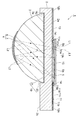
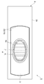
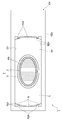
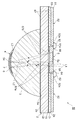
도 1은 본 발명에 관한 분광모듈의 제1 실시형태의 평면도이고, 도 2는 도 1의 II-II선에 따른 단면도이다. 도 1, 2에 나타내는 바와 같이, 분광모듈(1)은 전면(前面)(한쪽의 면)(2a)으로부터 입사한 광(L1)을 투과시키는 기판(2)과, 기판(2)에 입사한 광(L1)을 투과시키는 렌즈부(광투과부)(3)와, 렌즈부(3)에 입사한 광(L1)을 분광하고, 아울러, 반사하는 분광부(4)와, 분광부(4)에 의해서 반사된 광(L2)을 검출하는 광검출소자(5)를 구비하고 있다. 분광모듈(1)은 광(L1)을 분광부(4)에서 복수의 파장에 대응한 광(L2)으로 분광하고, 그 광(L2)을 광검출소자(5)에서 검출함으로써, 광(L1)의 파장분포나 특정파장성분의 강도 등을 측정하는 마이크로 분광모듈이다.1 is a plan view of a first embodiment of a spectroscopic module according to the present invention, and FIG. 2 is a cross-sectional view taken along the line II-II of FIG. 1. As shown in Figs. 1 and 2, the
기판(2)은 BK7, 파이렉스(Pyrex)(등록상표), 석영 등의 광투과성 유리, 플라스틱 등에 의해서, 장방형(長方形) 판상(板狀)(예를 들면, 전체 길이 15 ~ 20㎜, 전체 폭 11 ~ 12㎜, 두께 1 ~ 3㎜)으로 형성되어 있다. 기판(2)의 전면(2a)에는 Al나 Au 등의 단층막 혹은 Cr-Pt-Au, Ti-Pt-Au, Ti-Ni-Au, Cr-Au 등의 적층막으로 이루어진 배선(11)이 형성되어 있다. 배선(11)은 기판(2)의 중앙부에 배치된 복수의 패드부(11a), 기판(2)의 길이방향에서의 일단부에 배치된 복수의 패드부(11b) 및 대응하는 패드부(11a)와 패드부(11b)를 접속하는 복수의 접속부(11c)를 가지고 있다. 또, 배선(11)은 CrO 등의 단층막 혹은 Cr-CrO 등의 적층막으로 이루어지는 광반사방지층(11d)을 기판(2)의 전면(2a) 측에 가지고 있다.The board |
또한, 기판(2)의 전면(2a)에는 기판(2)에 광검출소자(5)를 위치결정하기 위한 '十'자 모양의 얼라이먼트 마크(기준부)(12a, 12b, 12c, 12d)가 배선(11)과 동일한 구성에 의해서 형성되어 있다. 얼라이먼트 마크(12a, 12b)는 기판(2)의 길이방향의 양단부에 각각 형성되어 있고, 기판(2)의 길이방향과 대략 직교하는 방향에서의 중앙위치에 배치되어 있다. 또, 얼라이먼트 마크(12c, 12d)는 기판(2)의 길이방향과 대략 직교하는 방향에서의 양단부에 각각 형성되어 있고, 기판(2)의 길이방향의 중앙위치에 배치되어 있다.In addition, an alignment mark (reference part) 12a, 12b, 12c, and 12d having a 'twelve' shape for positioning the
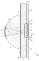
도 3은 도 1의 분광모듈의 분해사시도이고, 도 4는 도 1의 분광모듈의 하면도이다. 도 3, 4에 나타내는 바와 같이, 기판(2)의 후면(다른 쪽의 면)(2b)에는 렌즈부(3)가 끼워맞춰지는 오목부(19)가 형성되어 있다. 오목부(19)는 기판(2)의 후면(2b)과 대략 평행한 바닥면(21) 및 바닥면(21)에 대략 수직인 측벽(제1 끼워맞춤부(후술하는 그레이팅홈(6a)의 연재방향에서 대향하는 측벽) 및 제2 끼워맞춤부(후술하는 그레이팅홈(6a)의 연재방향과 대략 직교하는 방향에서 대향하는 측벽))(22)로 이루어지고, 얼라이먼트 마크(12a, 12b, 12c, 12d)에 대해서 소정의 위치관계를 가지도록 에칭에 의해서 형성되어 있다. 또, 오목부(19)는 기판(2)의 길이방향과 대략 직교하는 방향에서 형성되는 렌즈부(3)와 측벽(22)과의 틈새에 비해, 기판(2)의 길이방향에서 형성되는 렌즈부(3)와 측벽(22)과의 틈새가 작아지도록 형성되어 있다(예를 들면, 기판(2)의 길이방향과 대략 직교하는 방향에서 형성되는 틈새가 0 ~ 100㎛, 기판(2)의 길이방향에서 형성되는 틈새가 0 ~ 30㎛).3 is an exploded perspective view of the spectral module of FIG. 1, and FIG. 4 is a bottom view of the spectral module of FIG. 1. As shown in FIG. 3, 4, the recessed
도 5는 도 1의 분광모듈의 렌즈부의 사시도이다. 도 5에 나타내는 바와 같이, 렌즈부(3)는 기판(2)과 동일한 재료, 광투과성 수지, 광투과성의 무기·유기 하이브리드 재료 혹은 광투과성 저융점유리, 플라스틱 등에 의해서 반구모양의 렌즈가 그 바닥면(3a)과 대략 직교하고 또한 서로 대략 평행한 2개의 평면으로 잘라내어 측면(3b)이 형성된 형상(예를 들면 곡률반경 6 ~ 10㎜, 바닥면(3a)의 전체 길이 12 ~ 18㎜, 바닥면(3a)의 전체 폭(즉 측면(3b)간 거리) 6 ~ 10㎜, 높이 5 ~ 8㎜)으로 형성되어 있고, 분광부(4)에 의해서 분광된 광(L2)을 광검출소자(5)의 광검출부(5a)에 결상(結像)하는 렌즈로서 기능한다. 또한, 렌즈형상은 구면렌즈에 한정하지 않고, 비구면렌즈라도 된다.5 is a perspective view of a lens unit of the spectral module of FIG. 1. As shown in FIG. 5, the
도 2, 3에 나타내는 바와 같이, 렌즈부(3)는 광학수지제(16)를 통하여 오목부(19)에 끼워맞춰져 있다. 즉, 렌즈부(3)는 기판(2)의 후면(2b) 측에 배치되어 있다. 구체적으로는, 렌즈부(3)는 렌즈부(3)와 오목부(19)의 측벽(22)과의 사이에 틈새가 형성되도록 끼워맞춰져 있고, 이들 틈새 및 렌즈부(3)의 바닥면(3a)과 오목부(19)의 바닥면(21)과의 사이에 광학수지제(16)가 개재하고 있다.As shown in FIGS. 2 and 3, the
도 2 ~ 4에 나타내는 바와 같이, 분광부(4)는 렌즈부(3)의 외측 표면에 형성된 회절층(6)과, 회절층(6)의 외측 표면에 형성된 반사층(7)을 가지는 반사형 그레이팅이다. 회절층(6)은 기판(2)의 길이방향을 따라서 복수의 그레이팅홈(6a)이 병설되는 것에 의해서 형성되고, 그레이팅홈(6a)의 연재방향은 기판(2)의 길이방향과 대략 직교하는 방향과 대략 일치한다. 회절층(6)은, 예를 들면, 톱니모양 단면의 블레이즈드 그레이팅(blazed grating), 직사각형 모양 단면의 바이너리 그레이팅(binary grating), 정현파(正弦波) 모양 단면의 홀로그래픽 그레이팅(holographic grating) 등이 적용되고, 광경화성의 에폭시수지, 아크릴수지 또는 유기무기 하이브리드 수지 등의 레플리카(replica)용 광학수지를 광경화시킴으로써 형성된다. 반사층(7)은 막모양으로서, 예를 들면, 회절층(6)의 외측 표면에 Al이나 Au 등을 증착하는 것으로 형성된다. 또한, 반사층(7)을 형성하는 면적을 조정함으로써, 분광모듈(1)의 광학 NA를 조정할 수 있다. 또, 렌즈부(3)와 분광부(4)를 구성하는 회절층(6)을 상기의 재료에 의해 일체로 형성하는 것도 가능하다.As shown in FIGS. 2-4, the
도 1, 2에 나타내는 바와 같이, 광검출소자(5)는 장방형 판상(예를 들면, 전체 길이 5 ~ 10㎜, 전체 폭 1.5 ~ 3㎜, 두께 0.1 ~ 0.8㎜)으로 형성되어 있다. 광검출소자(5)의 광검출부(5a)는 CCD 이미지센서, PD 어레이 혹은 CMOS 이미지센서 등이며, 복수의 채널이 분광부(4)의 그레이팅홈(6a)의 연재방향과 대략 직교하는 방향(즉 그레이팅홈(6a)의 병설방향)으로 배열되어 이루어진다.As shown in FIG. 1, 2, the
광검출부(5a)가 CCD 이미지센서인 경우, 2차원적으로 배치되어 있는 화소에 입사된 위치에서의 광의 강도정보가 라인 비닝(line binning)됨으로써, 1차원의 위치에서의 광의 강도정보로 되어, 그 1차원의 위치에서의 광의 강도정보가 시계열(時系列)적으로 읽어 내진다. 즉, 라인 비닝되는 화소의 라인이 1채널이 된다. 광검출부(5a)가 PD 어레이 또는 CMOS 이미지센서인 경우, 1차원적으로 배치되어 있는 화소에 입사된 위치에서의 광의 강도정보가 시계열적으로 읽어 내지기 때문에, 1화소가 1채널이 된다.In the case where the
또한, 광검출부(5a)가 PD 어레이 또는 CMOS 이미지센서로서, 화소가 2차원 배열되어 있는 경우에는 분광부(4)의 그레이팅홈(6a)의 연재방향과 평행한 1차원 배열방향으로 늘어선 화소의 라인이 1채널이 된다. 또, 광검출부(5a)가 CCD 이미지센서인 경우, 예를 들면, 배열방향에서의 채널끼리의 간격이 12.5㎛, 채널 전체 길이(라인 비닝되는 1차원 화소열의 길이)가 1㎜, 배열되는 채널의 수가 256인 것이 광검출소자(5)에 이용된다.In addition, when the
또, 광검출소자(5)에는 채널의 배열방향에서 광검출부(5a)와 병설되고, 분광부(4)로 진행하는 광(L1)이 통과하는 광통과구멍(5b)이 형성되어 있다. 광통과구멍(5b)은 기판(2)의 길이방향과 대략 직교하는 방향으로 연재하는 슬릿(예를 들면, 길이 0.5 ~ 1㎜, 폭 10 ~ 100㎛)이고, 광검출부(5a)에 대해서 고정밀도로 위치결정된 상태에서 에칭 등에 의해서 형성되어 있다.In the
또, 기판(2)의 전면(2a)에는 배선(11)의 패드부(11a, 11b) 및 얼라이먼트 마크(12a, 12b, 12c, 12d)를 노출시키고 또한 배선(11)의 접속부(11c)를 덮도록 흡광층(13)이 형성되어 있다. 흡광층(13)에는 분광부(4)로 진행하는 광(L1)이 통과하도록 광검출소자(5)의 광통과구멍(5b)과 대향하는 위치에 슬릿(13a)이 형성되고, 또한, 광검출소자(5)의 광검출부(5a)로 진행하는 광(L2)이 통과하도록 광검출부(5a)와 대향하는 위치에 개구부(13b)가 형성된다. 흡광층(13)은 소정의 형상으로 패터닝되어, CrO, CrO를 포함한 적층막 혹은 블랙 레지스터 등에 의해서 일체 성형된다.Moreover, the
흡광층(13)으로부터 노출한 패드부(11a)에는 광검출소자(5)의 외부단자가 범프(bump)(14)를 통한 페이스다운 본딩(facedown bonding)에 의해서 전기적으로 접속되어 있다. 또, 패드부(11b)는 외부의 전기소자(미도시)와 전기적으로 접속된다. 그리고, 광검출소자(5)의 기판(2) 측(여기에서는, 광검출소자(5)와 기판(2) 또는 흡광층(13)과의 사이)에는 적어도 광(L2)을 투과시키는 언더필(underfill)재(15)가 충전되며, 이것에 의해서, 기계강도를 유지할 수 있다.The external terminal of the
상술한 분광모듈(1)의 제조방법에 대해 설명한다.The manufacturing method of the
우선, 기판(2)의 전면(2a)에 배선(11) 및 얼라이먼트 마크(12a, 12b, 12c, 12d)를 패터닝한다. 그 후, 패드부(11a, 11b) 및 얼라이먼트 마크(12a, 12b, 12c, 12d)가 노출되고, 슬릿(13a) 및 개구부(13b)가 형성되도록 흡광층(13)을 패터닝한다. 이 흡광층(13)은 포토리소그래피에 의해 얼라이먼트하여 형성된다. 또, 양면 얼라이먼트 노광장치 등을 이용한 포토리소그래피와 에칭에 의해, 기판(2)의 후면(2b)에 전면(2a)에 형성된 얼라이먼트 마크(12a, 12b, 12c, 12d)에 대해서 소정의 위치관계를 가지도록 오목부(19)를 형성한다.First, the
흡광층(13) 위에는 광검출소자(5)가 페이스다운 본딩에 의해서 실장된다. 이 때, 광검출소자(5)는 광검출부(5a)의 채널의 배열방향이 기판(2)의 길이방향과 대략 일치하고 또한 광검출부(5a)가 기판(2)의 전면(2a) 측을 향하도록 배치되며, 화상인식에 의해서 얼라이먼트 마크(12a, 12b, 12c, 12d)를 기준으로 한 소정의 위치에 실장된다.On the
그 한편으로, 렌즈부(3)에 분광부(4)를 형성한다. 우선, 렌즈부(3)의 정점(頂点) 부근에 떨어뜨린 레플리카용 광학수지에 대해서, 회절층(6)에 대응하는 그레이팅이 새겨진 광투과성의 마스터 그레이팅(미도시)을 맞닿게 한다. 다음으로, 레플리카용 광학수지에 마스터 그레이팅을 맞닿게 한 상태에서 광을 비추어 경화시킴으로써, 기판(2)의 길이방향과 대략 직교하는 방향으로 연재하는 복수의 그레이팅홈(6a)을 가지는 회절층(6)을 형성한다. 또한, 경화시킨 후에는 가열큐어(cure)를 행함으로써 안정화시키는 것이 바람직하다. 레플리카용 광학수지가 경화하면 마스터 그레이팅을 이형(離型)하여, 회절층(6)의 외면에 알루미늄이나 금을 마스크 증착 혹은 전면(全面) 증착함으로써 반사층(7)을 형성한다.On the other hand, the
이어서, 기판(2)의 오목부(19)에 광경화성의 광학수지제(16)를 도포한다. 그리고, 렌즈부(3)의 바닥면(3a) 측을 오목부(19)에 끼워맞춘다. 이 때, 렌즈부(3)는 분광부(4)의 그레이팅홈(6a)의 연재방향이 기판(2)의 길이방향과 대략 직교하는 방향으로 대략 일치하도록 끼워맞춰지고, 렌즈부(3)와 오목부(19)의 측벽(22)과의 틈새로부터는 여분의 수지제나 공기가 빼내진다. 그 후, 광을 비추어 광학수지제(16)를 경화시킴으로써, 렌즈부(3)를 기판(2)에 실장한다.Next, the photocurable
상술한 분광모듈(1)의 작용효과에 대해서 설명한다.The effect of the above-mentioned
이 분광모듈(1)에서는 기판(2)에 광검출소자(5)를 위치결정하기 위한 얼라이먼트 마크(12a, 12b, 12c, 12d)에 대해서 오목부(19)가 소정의 위치관계를 가지고 있기 때문에, 분광부(4)가 형성된 렌즈부(3)를 오목부(19)에 끼워맞춰지게 하는 것만으로, 분광부(4) 및 렌즈부(3)가 기판(2)에 대해서 위치결정된다. 또, 분광모듈(1)에서는 얼라이먼트 마크(12a, 12b, 12c, 12d)에 의해서 광검출소자(5)가 기판(2)에 위치결정되어 있기 때문에, 분광부(4)가 기판(2)에 대해서 위치결정됨으로써, 결과적으로 분광부(4)와 광검출소자(5)와의 얼라이먼트가 실현된다. 따라서, 이 분광모듈(1)에 의하면, 이른바 패시브 얼라이먼트가 실현되기 때문에, 분광모듈의 간편한 조립이 가능하게 된다.In the
또, 이 분광모듈(1)에서는 오목부(19)가 측벽(22)과 렌즈부(3)와의 틈새가 그레이팅홈(6a)의 연재방향(즉 기판(2)의 길이방향과 대략 직교하는 방향)에서의 틈새에 비하여, 그레이팅홈(6a)의 연재방향과 대략 직교하는 방향(즉 기판(2)의 길이방향)과 대략 일치하는 방향에서의 틈새가 작아지도록 형성되어 있다. 따라서, 이 분광모듈(1)에 의하면, 그레이팅홈(6a)의 연재방향과 대략 직교하는 방향에서는 렌즈부(3)와 광검출소자(5)와의 얼라이먼트가 정밀도 좋게 행해지기 때문에, 분광부(4)에 의해서 분광된 광(L2)을 정확하게 광검출소자(5)에 입사시킬 수 있어, 분광모듈의 신뢰성을 향상시키는 것이 가능하게 된다. 그리고, 이 분광모듈(1)에서는 광검출소자(5)에서의 채널(화소의 라인)의 배열방향과 기판(2)의 길이방향이 대략 일치하고 있기 때문에, 채널의 배열방향(즉 그레이팅홈(6a)의 연재방향과 대략 직교하는 방향)에서는 렌즈부(3)와 광검출소자(5)와의 얼라이먼트가 정밀도 좋게 행해지게 된다. 따라서, 이 분광모듈(1)에 의하면, 분광부(4)에 의해서 분광된 광(L2)이 채널의 배열방향(채널의 폭방향)으로 어긋나지 않고 적절한 채널 내에 입사되기 때문에, 분광모듈의 신뢰성의 향상이 효과적으로 도모된다.In the
또, 분광모듈(1)에 의하면, 그레이팅홈(6a)의 연재방향에서는 렌즈부(3)와 측벽(22)과의 틈새가 보다 크게 형성되기 때문에, 광학수지제에 의해 렌즈부(3)를 기판(2)에 접착할 때, 그레이팅홈(6a)의 연재방향의 틈새로부터 여분의 수지나 공기를 효과적으로 빼낼 수 있다. 따라서, 이 분광모듈(1)에 의하면, 렌즈부(3)와 기판(2)과의 사이(즉 렌즈부(3)와 오목부(19)와의 사이)에서의 광학수지제(16)의 편향이나 기포 발생이 억제되기 때문에, 기판(2)에 대해서 렌즈부(3)를 정밀도 좋게 실장하는 것이 가능하게 된다.Further, according to the
본 발명은, 상술한 제1 실시형태에 한정되는 것은 아니다.The present invention is not limited to the above-described first embodiment.
예를 들면, 도 6에 나타내는 바와 같이, 오목부(33)는 기판(32)의 후면(32b)과 대략 평행한 장방형 모양의 바닥면(34) 및 바닥면(34)에 대략 수직인 측벽(35)으로 이루어지고, 측벽(35)은 기판(32)의 길이방향 및 길이방향과 대략 직교하는 방향에서 렌즈부(3)가 끼워맞춰지는 끼워맞춤부(35a)와, 렌즈부(3)로부터 이간하는 이간부(35b)를 가지고 있어도 된다. 이 경우, 렌즈부(3)를 기판(32)에 실장할 때, 렌즈부(3)와 이간부(35b)와의 사이에 형성된 틈새(M)로부터 여분의 수지나 공기를 빼낼 수 있기 때문에, 렌즈부(3)와 기판(32)과의 사이에 수지의 편향이나 기포가 생기지 않고, 렌즈부(3)의 확실한 고정이 도모되며, 아울러, 렌즈부(3)와 바닥면(34)와의 사이의 수지의 두께가 대략 균일하게 되어 기판(32)에 대한 수평 정밀도가 높은 렌즈부(3)의 실장이 가능하게 된다.For example, as shown in FIG. 6, the recessed
또, 도 7에 나타내는 바와 같이, 오목부(43)는 기판(42)의 후면(42b)과 대략 평행한 대략 장방형 모양의 바닥면(44) 및 바닥면(44)에 대략 수직인 측벽(45)으로 이루어지고, 측벽(45)은 기판(42)의 길이방향을 따라서 오목부(43) 내측으로 돌출한 2쌍의 볼록부(45a)의 일부를 포함하며, 기판(42)의 길이방향 및 길이방향과 대략 직교하는 방향에서 렌즈부(3)가 끼워맞춰지는 끼워맞춤부(45b)와, 렌즈부(3)로부터 이간하는 이간부(45c)를 가지고 있어도 된다. 이 경우, 렌즈부(3)를 기판(42)에 실장할 때, 끼워맞춤부(45b)가 오목부(43) 내측으로 돌출한 볼록부(45a)의 일부를 포함하기 때문에, 제1 실시형태와 비교해서 렌즈부(3)와 이간부(45c)와의 틈새(N)가 보다 크게 형성되어, 효과적으로 여분의 수지나 공기를 빼내는 것이 가능하게 된다.In addition, as shown in FIG. 7, the recessed
또, 도 6, 7에 나타내는 바와 같이, 이간부는 렌즈부(3)를 둘러싸도록 복수 마련되어 있어도 된다. 이 구성에 의하면, 렌즈부(3)와 이간부와의 틈새가 렌즈부(3)를 둘러싸도록 복수 형성되기 때문에, 광학수지제에 의해 렌즈부(3)를 기판에 접착할 때, 렌즈부(3)를 둘러싸는 복수의 틈새로부터 여분의 수지나 공기를 효율 좋게 빼낼 수 있다.6 and 7, a plurality of separation portions may be provided to surround the
또, 도 6, 7에 나타나는 오목부는 기판의 길이방향과 대략 직교하는 방향에서의 렌즈부(3)와 오목부의 측면과의 틈새에 비하여, 기판의 길이방향과 대략 일치하는 방향에서의 렌즈부(3)와 오목부의 측면과의 틈새가 작아지도록 형성되어 있어도 된다. 이 경우, 보다 효과적으로 여분의 수지나 공기를 빼낼 수 있다.6 and 7, the recessed portion shown in FIGS. 6 and 7 has a lens portion in a direction substantially coincident with the longitudinal direction of the substrate as compared with the gap between the
또, 오목부는 기판의 에칭이 아니고, 레지스터 등의 수지나 메탈 마스크에 의해서 기판상으로 형성되어 있어도 된다.Moreover, the recessed part may not be etching of a board | substrate but may be formed in the board | substrate by resin, such as a resistor, and a metal mask.
또, 기준부는 얼라이먼트 마크(12a, 12b, 12c, 12d)에 한정되지 않고, 예를 들면 배선(11)을 기준부로서 이용하고, 오목부(19) 및 광검출소자(5)의 위치맞춤을 행해도 된다. 또, 예를 들면 기판(2)의 외형에서의 코너부를 기준부로서 이용해도 된다.The reference portion is not limited to the alignment marks 12a, 12b, 12c, and 12d. For example, the reference portion is used as the reference portion, and the
[제2 실시형태]Second Embodiment
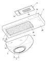
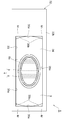
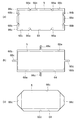
도 8은 본 발명에 관한 분광모듈의 제2 실시형태의 평면도이며, 도 9는 도 8의 IX-IX선에 따른 단면도이다. 도 8, 9에 나타내는 바와 같이, 분광모듈(10)은 전면(한쪽의 면)(2a) 측으로부터 입사한 광(L1)을 투과시키는 기판(본체부)(2)과, 기판(2)에 입사한 광(L1)을 투과시키는 렌즈부(본체부)(3)와, 렌즈부(3)에 입사한 광(L1)을 분광하고, 아울러, 반사하는 분광부(4)와, 분광부(4)에 의해서 반사된 광(L2)을 검출하는 광검출소자(5)를 구비하고 있다.8 is a plan view of a second embodiment of a spectroscopic module according to the present invention, and FIG. 9 is a cross-sectional view taken along the line IX-IX of FIG. 8. As shown in FIGS. 8 and 9, the
기판(2)은 장방형 판상으로 형성되어 있고, 기판(2)의 전면(2a)에는 광검출소자(5)가 배치되는 단면 장방형 모양의 개구부(51a)가 형성된 장방형 판상의 배선기판(51)이 수지제(53)에 의해서 접착되어 있다. 배선기판(51)에는 금속재료로 이루어진 배선(52)이 마련되어 있다. 배선(52)은 개구부(51a)의 주위에 배치된 복수의 패드부(52a), 배선기판(51)의 길이방향에서의 양단부에 배치된 복수의 패드부(52b) 및 대응하는 패드부(52a)와 패드부(52b)를 접속하는 복수의 접속부(52c)를 가지고 있다.The board |
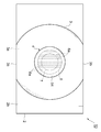
도 10은 도 8의 분광모듈의 하면도이다. 도 9, 10에 나타내는 바와 같이, 렌즈부(3)는 기판(2)의 각부(角部)나 변부(邊部) 등, 기판(2)의 외연부를 기준부로 하여 광(L1, L2)을 투과시키는 광학수지제(16)에 의해서 기판(2)의 후면(다른 쪽의 면)(2b)에 접착되어 있다. 이 때, 분광부(4)는 렌즈부(3)에 대해서 고정밀도로 위치결정되어 있기 때문에, 기판(2)의 외연부는 기판(2)에 분광부(4)를 위치결정하기 위한 기준부가 된다.10 is a bottom view of the spectral module of FIG. 8. As shown in FIGS. 9 and 10, the
분광부(4)는 렌즈부(3)의 외측 표면에 형성된 회절층(6), 회절층(6)의 외측 표면에 형성된 반사층(7) 및 회절층(6) 및 반사층(7)을 덮는 패시베이션(passivation)층(54)을 가지는 반사형 그레이팅이다. 회절층(6)은 기판(2)의 길이방향을 따라서 복수의 그레이팅홈(6a)이 병설됨으로써 형성되고, 그레이팅홈(6a)의 연재방향은 기판(2)의 길이방향과 대략 직교하는 방향과 대략 일치한다.The
도 8, 9에 나타내는 바와 같이, 광검출소자(5)는 장방형 판상으로 형성되어 있고, 광검출소자(5)의 분광부(4) 측의 면에는 광검출부(5a)가 형성되어 있다. 광검출부(5a)는 CCD 이미지센서, PD 어레이 혹은 CMOS 이미지센서 등이며, 복수의 채널이 분광부(4)의 그레이팅홈(6a)의 연재방향과 대략 직교하는 방향(즉 그레이팅홈(6a)의 병설방향)으로 배열되어 이루어진다.As shown in FIG. 8, 9, the
또, 광검출소자(5)에는 채널의 배열방향에서 광검출부(5a)와 병설되고, 분광부(4)로 진행하는 광(L1)이 통과하는 광통과구멍(5b)이 형성되어 있다. 광통과구멍(5b)은 기판(2)의 길이방향과 대략 직교하는 방향으로 연재하는 슬릿이며, 광검출부(5a)에 대해서 고정밀도로 위치결정된 상태에서 에칭 등에 의해서 형성되어 있다.In the
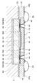
도 11은 도 9의 분광모듈의 주요부 확대단면도이다. 도 11에 나타내는 바와 같이, 광검출소자(5)는 광(L1, L2)을 투과시키는 광학수지제(55)에 의해서 광검출소자(5)의 분광부(4) 측의 면에 접착된 광투과판(56) 및 광검출소자(5)의 분광부(4)와 반대 측의 면에서 광검출부(5a)와 대향하는 부분에 형성된 차광막(57)을 가지고 있다. 광투과판(56)은 광검출부(5a) 및 광통과구멍(5b)을 덮고 있다. 차광막(57)은 광통과구멍(5b)을 통하지 않고 분광부(4)로 진행하려고 하는 광(L1)이나, 광검출부(5a)에 직접 입사하려고 하는 광(L1)을 차광한다. 또한, 배선기판(51)도, 차광막(57)과 마찬가지로, 광통과구멍(5b)을 통하지 않고 분광부(4)로 진행하려고 하는 광(L1)을 차광하는 기능을 가지고 있다.11 is an enlarged cross-sectional view of a main part of the spectral module of FIG. 9. As shown in FIG. 11, the light-detecting
광검출소자(5)의 분광부(4) 측의 면에는 전극(58)이 복수 형성되어 있고, 광검출소자(5)의 분광부(4)와 반대 측의 면에는 각 전극(58)과 관통전극(59)에 의해서 접속된 단자전극(61)이 복수 형성되어 있다. 각 단자전극(61)은 대응하는 배선기판(51)의 패드부(52a)와 와이어(62)에 의해서 접속되어 있다. 이것에 의해, 광검출부(5a)에서 발생한 전기신호는 전극(58), 관통전극(59), 단자전극(61), 패드부(52a), 접속부(52c) 및 패드부(52b)를 통하여 외부로 취출된다.A plurality of
광투과판(56)의 광검출소자(5) 측의 면에는 흡광층(68)이 형성되어 있다. 흡광층(68)에는 분광부(4)로 진행하는 광(L1)이 통과하도록 광검출소자(5)의 광통과구멍(5b)과 대향하는 위치에 광통과구멍(68a)가 형성됨과 동시에, 광검출소자(5)의 광검출부(5a)로 진행하는 광(L2)이 통과하도록 광검출부(5a)와 대향하는 위치에 광통과구멍(68b)이 형성되어 있다. 흡광층(68)은 소정의 형상으로 패터닝되고, CrO, CrO를 포함한 적층막 혹은 블랙 레지스터 등에 의해서 일체 성형된다. 또한, 흡광층(68)은, 도 12에 나타내는 바와 같이, 광검출소자(5)의 분광부(4) 측의 면에 형성되어 있어도 된다.The
도 11에 나타내는 바와 같이, 기판(2)의 전면(2a)에는 광(L1, L2)을 투과시키는 광학수지제(63)를 통하여 광검출소자(5)가 끼워맞춰지는 단면 장방형 모양의 오목부(64)가 형성되어 있다. 오목부(64)는 기판(2)의 전면(2a)과 대략 평행한 바닥면(65) 및 바닥면(65)에 대략 수직인 측벽(66)으로 이루어지고, 기판(2)에 분광부(4)를 위치결정하기 위한 기준부가 되는 기판(2)의 외연부에 대해서 소정의 위치관계를 가지도록 에칭에 의해서 형성되어 있다. 또한, 광검출소자(5)는 오목부(64)에 끼워맞춰진 상태에서 기판(2)의 전면(2a)으로부터 돌출하고 있다.As shown in FIG. 11, the front-
도 13은 도 8의 분광모듈에서의 광검출소자와 오목부와의 관계를 나타내는 도면이다. 도 13에 나타내는 바와 같이, 오목부(64)에는 분광부(4)의 그레이팅홈(6a)의 연재방향에서 광검출소자(5)와 끼워맞춰지는 측벽(제3 끼워맞춤부)(66a) 및 분광부(4)의 그레이팅홈(6a)의 연재방향과 대략 직교하는 방향에서 광검출소자(5)와 끼워맞춰지는 측벽(제4 끼워맞춤부)(66b)이 마련되어 있다. 측벽(66b)과 광검출소자(5)와의 틈새는 측벽(66a)과 광검출소자(5)와의 틈새보다도 작게 되어 있다.FIG. 13 is a diagram illustrating a relationship between a light detecting element and a recess in the spectral module of FIG. 8. As shown in FIG. 13, the recessed
상술한 분광모듈(10)의 제조방법에 대해 설명한다.The manufacturing method of the
우선, 렌즈부(3)에 분광부(4)를 형성한다. 구체적으로는 렌즈부(3)의 정점 부근으로 떨어진 레플리카용 광학수지에 대해, 회절층(6)에 대응하는 그레이팅이 새겨진 광투과성의 마스터 그레이팅을 눌러 닿게 한다. 그리고, 이 상태에서 광을 조사함으로써 레플리카용 광학수지를 경화시키고, 바람직하게는, 안정화시키기 위해서 가열큐어를 행함으로써, 복수의 그레이팅홈(6a)을 가지는 회절층(6)을 형성한다. 그 후, 마스터 그레이팅을 이형하여, 회절층(6)의 외측 표면에 Al나 Au 등을 증착함으로써 반사층(7)을 형성하며, 또한, 회절층(6) 및 반사층(7)의 외측 표면에 MgF2 등을 증착함으로써 패시베이션층(54)을 형성한다.First, the
그 한편으로, 기판(2)을 준비하고, 양면 얼라이먼트 노광장치 등을 이용한 포토리소그래피와 에칭에 의해, 기판(2)의 각부나 변부 등, 기판(2)의 외연부를 기준부로 하여, 그 기준부에 대해서 소정의 위치관계를 가지도록 기판(2)의 전면(2a)에 오목부(64)를 형성한다.On the other hand, the
이어서, 분광부(4)가 형성된 렌즈부(3)를 기판(2)의 각부나 변부 등, 기판(2)의 외연부를 기준부로 하여, 광학수지제(16)에 의해서 기판(2)의 후면(2b)에 접착한다. 그 후, 기판(2)의 오목부(64)에 광학수지제(63)를 도포하여, 광투과판(56)이 접합된 광검출소자(5)를 오목부(64)에 끼워맞춘다. 그리고, 광을 조사함으로써 광학수지제(63)를 경화시켜 광검출소자(5)를 기판(2)에 실장한다.Subsequently, the rear surface of the
이어서, 배선기판(51)을 수지제(53)에 의해서 기판(2)의 전면(2a)에 접착한다. 그리고, 대응하는 광검출소자(5)의 단자전극(61)과 배선기판(51)의 패드부(52a)를 와이어(62)에 의해서 접속하여 분광모듈(10)을 얻는다.Subsequently, the
이상 설명한 바와 같이, 분광모듈(10)에서는 기판(2)에 분광부(4)를 위치결정하기 위한 기준부인 기판(2)의 외연부에 대해서 오목부(64)가 소정의 위치관계를 가지고 있기 때문에, 광검출소자(5)를 오목부(64)에 끼워맞춰지게 하는 것만으로, 광검출소자(5)가 기판(2)에 위치결정된다. 이 때, 분광부(4)가 형성된 렌즈부(3)가 기준부인 기판(2)의 외연부에 의해서 기판(2)에 위치결정되기 때문에, 결과적으로, 분광부(4)와 광검출소자(5)와의 얼라이먼트가 실현된다. 게다가, 분광부(4)의 그레이팅홈(6a)의 연재방향과 대략 직교하는 방향에서의 오목부(64)의 측벽(66)과 광검출소자(5)와의 틈새가 분광부(4)의 그레이팅홈(6a)의 연재방향에서의 오목부(64)의 측벽(66)과 광검출소자(5)와의 틈새보다도 작게 되어 있다. 이것에 의해, 그레이팅홈(6a)의 연재방향과 대략 직교하는 방향에서는 렌즈부(3)와 광검출소자(5)와의 얼라이먼트가 정밀도 좋게 행해지기 때문에, 분광부(4)에 의해서 분광된 광(L2)을 정확하게 광검출소자(5)에 입사시킬 수 있다. 또한, 광검출소자(5)가 장방형 판상이기 때문에, 그레이팅홈(6a)의 연재방향에서는 광검출소자(5)와 오목부(64)의 측벽(66)과의 틈새가 보다 길게 형성되며, 틈새에 이르는 거리도 보다 짧게 되기 때문에, 광학수지제(63)에 의해서 광검출소자(5)를 기판(2)에 접착할 때, 여분의 수지나 공기를 효과적으로 빼낼 수 있다. 이와 같이, 분광모듈(10)에 의하면, 이른바 패시브 얼라이먼트가 실현되기 때문에, 신뢰성을 유지하면서 간편하게 조립하는 것이 가능하게 된다.As described above, in the
또, 분광모듈(10)에서는 광검출소자(5)가 오목부(64)에 끼워맞춰진 상태에서, 기판(2)의 전면(2a)으로부터 돌출하고 있다. 이것에 의해, 기판(2)의 전면(2a)에 형성된 오목부(64)에 광검출소자(5)를 끼워맞추는 작업을 용이화할 수 있을 뿐만 아니라, 오목부(64)의 바닥면(65)에 광검출소자(5)를 확실히 밀어붙여 여분의 수지나 공기를 확실히 빼낼 수 있다.In the
또한, 분광모듈(10)에서는 광검출소자(5)에 분광부(4)로 진행하는 광(L1)이 통과하는 광통과구멍(5b)이 형성되어 있다. 이것에 의해, 분광부(4) 및 광검출소자(5)에 대한 광통과구멍(5b)의 패시브 얼라이먼트를 실현시킬 수 있다.In the
본 발명은, 상술한 제2 실시형태에 한정되는 것은 아니다.This invention is not limited to 2nd Embodiment mentioned above.
예를 들면, 도 14에 나타내는 바와 같이, 복수 층의 기판을 접합시킴으로써 기판(2)을 구성해도 된다. 일례로서 2층의 기판(21, 22)이 광학수지제(16)에 의해서 접합되어 기판(2)이 구성되어 있는 경우, 분광부(4)과 반대 측에 배치되는 기판(21)에 단면 장방형 모양의 개구부를 형성함으로써, 기판(2)의 오목부(64)를 형성해도 된다.For example, as shown in FIG. 14, you may comprise the board |
또, 서로 인접하는 기판(21)과 기판(22)과의 사이나, 기판(22)과 렌즈부(3)와의 사이에 분광부(4)로 진행하는 광(L1)이 통과하는 광통과구멍(67a) 및 광검출소자(5)의 광검출부(5a)로 진행하는 광(L2)이 통과하는 광통과구멍(67b)을 가지는 흡광층(67)을 형성해도 된다. 이 구성에 의하면, 넓어지면서 진행하는 광을 소망의 영역에 도달하도록 제한할 수 있고, 아울러, 광검출소자(5)에 미광(迷光, stray light)이 입사하는 것을 효과적으로 억제할 수 있다.Moreover, the light L1 which propagates to the
또한, 흡광층(67)의 재료로서는, 블랙 레지스터, 필러(카본이나 산화물 등)가 들어간 유색의 수지(실리콘, 엑폭시, 아크릴, 우레탄, 폴리이미드, 복합수지 등), Cr나 Co 등의 금속 또는 산화금속 혹은 그 적층막, 포러스(porous) 모양의 세라믹이나 금속 또는 산화금속을 들 수 있다. 또, 흡광층(67)에서 광통과구멍(67a, 67b)의 사이즈를 다르게 함으로써, 광학 NA를 조정할 수 있다.As the material of the
또, 도 14에 나타내는 바와 같이, 광검출소자(5)로서 이른바 이면(裏面) 입사형의 소자를 적용해도 된다. 이 경우에는, 전극(58)이 광검출부(5a)와 함께 외측에 위치하게 되므로, 전극(58)을 단자전극으로서 배선기판(51)의 패드부(52a)와 와이어(62)로 접속하면 된다. 또, 기판(2)과 렌즈부(3)를 몰드로 일체성형해도 되고, 렌즈부(3)와 회절층(6)을 레플리카 성형용의 광투과성 저융점유리 등에 의해서 일체적으로 형성해도 된다. 또, 본체부로서 기판(2)을 이용하지 않고, 렌즈부(3)의 전면에 오목부(64)를 형성해도 된다.As shown in FIG. 14, a so-called back incident element may be used as the
또, 도 15에 나타내는 바와 같이, 광검출소자(5)가 끼워맞춰지는 오목부(64)의 측벽(66)은 광검출소자(5)로부터 이간하는 이간부(66c)를 가지고 있어도 된다. 이와 같은 구조에 의하면, 광학수지제(63)에 의해서 광검출소자(5)를 기판(2)에 접착할 때, 광검출소자(5)와 이간부(66c)와의 틈새로부터 여분의 수지나 공기를 보다 효과적으로 빼낼 수 있다. 그 때문에, 광검출소자(5)와 기판(2)과의 사이에서의 수지제의 편향이나 기포의 발생을 억제하는 것이 가능하게 된다.As shown in FIG. 15, the
또한, 본 발명은 상술한 제1 및 제2 실시형태에 한정되는 것이 아니고, 기판(2)의 후면(2b)에 오목부(19)를 형성하고, 광학수지제(16)를 개재시켜 오목부(19)에 렌즈부(3)를 끼워맞추게 하고, 또한, 기판(2)의 전면(2a)에 오목부(64)를 형성하고, 광학수지제(63)를 개재시켜 오목부(64)에 광검출소자(5)를 끼워맞추게 하여도 된다. 이 경우에는, 일례로서 오목부(64)가 기판(2)에 광검출소자(5)를 위치결정하기 위한 기준부가 되며, 오목부(19)가 기판(2)에 분광부(4)를 위치결정하기 위한 기준부가 된다. 또, 분광부(4)로 진행하는 광(L1)이 통과하는 광통과구멍(5b)을 광검출소자(5)에 형성하지 않고, 별도, 배선기판이나 차광막에 형성해도 된다.In addition, this invention is not limited to the above-mentioned 1st and 2nd embodiment, The recessed
[산업상의 이용 가능성][Industrial Availability]
본 발명에 의하면, 분광모듈의 신뢰성을 유지하면서 분광모듈의 간편한 조립이 가능하게 된다.According to the present invention, it is possible to easily assemble the spectroscopic module while maintaining the reliability of the spectroscopic module.
1, 10 … 분광모듈, 2 … 기판(본체부), 2a … 전면(한쪽의 면), 2b … 후면(한쪽의 면), 3 … 렌즈부(광투과부, 본체부), 4 … 분광부, 5 … 광검출소자, 6a … 그레이팅홈, 16 … 광학수지제, 19 … 오목부, 22 … 측벽(제1 끼워맞춤부, 제2 끼워맞춤부), 63 … 광학수지제, 64 … 오목부, 66a … 측벽(제3 끼워맞춤부), 66b … 측벽(제4 끼워맞춤부).1, 10... Spectroscopic module, 2... Substrate (main body), 2a... Front side (one side), 2b... Rear (one side), 3... Lens portion (light transmitting portion, main body portion), 4. 5 spectroscopic section; Photodetector, 6a... Grating groove, 16... Optical resin, 19. 22,. Side wall (first fitting portion, second fitting portion), 63. Optical resin agent, 64. Recessed
Claims (8)
상기 기판의 다른 쪽의 면 측에 배치되어 상기 기판에 입사한 광을 투과시키는 광투과부와,
상기 광투과부에 형성되어 상기 광투과부에 입사한 광을 분광하고, 아울러, 반사하는 분광부와,
상기 기판의 상기 한쪽의 면 측에 배치되어 상기 분광부에 의해서 분광된 광을 검출하는 광검출소자를 구비하고,
상기 다른 쪽의 면에는 상기 기판에 상기 광검출소자를 위치결정하기 위한 기준부에 대해서 소정의 위치관계를 가지며, 광학수지제를 통하여 상기 광투과부가 끼워맞춰지는 오목부가 형성되어 있고,
상기 오목부에는 상기 분광부의 그레이팅홈의 연재(延在)방향에서 상기 광투과부와 끼워맞춰지는 제1 끼워맞춤부 및 상기 그레이팅홈의 연재방향과 대략 직교하는 방향에서 상기 광투과부와 끼워맞춰지는 제2 끼워맞춤부가 마련되어 있으며,
상기 제2 끼워맞춤부와 상기 광투과부와의 틈새는 상기 제1 끼워맞춤부와 상기 광투과부와의 틈새보다도 작게 되어 있는 것을 특징으로 하는 분광모듈.A substrate for transmitting light incident from one surface thereof,
A light transmitting portion disposed on the other surface side of the substrate and transmitting light incident on the substrate;
A spectroscopic portion formed on the light transmitting portion, for spectroscopy and reflects light incident on the light transmitting portion,
A photodetector disposed on the one side of the substrate and detecting light spectroscopy by the spectroscope;
On the other side, the substrate has a predetermined positional relationship with respect to the reference portion for positioning the light detecting element, and a concave portion into which the light transmitting portion is fitted through an optical resin is formed.
The concave portion is fitted with the light transmitting portion in a direction that is substantially orthogonal to the extending direction of the grating groove and the first fitting portion fitted with the light transmitting portion in the extending direction of the grating groove of the spectroscopic portion. The second fitting part is provided,
The clearance between the second fitting portion and the light transmitting portion is smaller than the clearance between the first fitting portion and the light transmitting portion.
상기 오목부의 측벽은 상기 제1 끼워맞춤부, 상기 제2 끼워맞춤부 및 상기 광투과부로부터 이간(離間)하는 이간부를 포함하는 것을 특징으로 하는 분광모듈.The method according to claim 1,
And the side wall of the concave portion includes a separation portion spaced apart from the first fitting portion, the second fitting portion, and the light transmitting portion.
상기 이간부는 상기 광투과부를 둘러싸도록 복수 마련되어 있는 것을 특징으로 하는 분광모듈.The method according to claim 2,
The separation module is provided with a plurality so as to surround the light transmitting portion.
상기 기판의 다른 쪽의 면 측에 배치되어 상기 기판에 입사한 광을 투과시키는 광투과부와,
상기 광투과부에 형성되어 상기 광투과부에 입사한 광을 분광하고, 아울러, 반사하는 분광부와,
상기 기판의 상기 한쪽의 면 측에 배치되어 상기 분광부에 의해서 분광된 광을 검출하는 광검출소자를 구비하고,
상기 다른 쪽의 면에는 상기 기판에 상기 광검출소자를 위치결정하기 위한 기준부에 대해서 소정의 위치관계를 가지는 오목부가 형성되어 있으며,
상기 광투과부는 상기 오목부에 끼워맞춰져 있는 것을 특징으로 하는 분광모듈.A substrate for transmitting light incident from one surface thereof,
A light transmitting portion disposed on the other surface side of the substrate and transmitting light incident on the substrate;
A spectroscopic portion formed on the light transmitting portion, for spectroscopy and reflects light incident on the light transmitting portion,
A photodetector disposed on the one side of the substrate and detecting light spectroscopy by the spectroscope;
On the other side, a concave portion having a predetermined positional relationship with a reference portion for positioning the light detecting element is formed on the substrate.
And the light transmitting portion is fitted to the concave portion.
상기 본체부에 형성되어 상기 본체부에 입사한 광을 분광하고, 아울러, 반사하는 분광부와,
상기 본체부의 상기 한쪽의 면 측에 배치되어 상기 분광부에 의해서 분광된 광을 검출하는 광검출소자를 구비하고,
상기 한쪽의 면에는 상기 본체부에 상기 분광부를 위치결정하기 위한 기준부에 대해서 소정의 위치관계를 가지며, 광학수지제를 통하여 상기 광검출소자가 끼워맞춰지는 오목부가 형성되어 있고,
상기 오목부에는 상기 분광부의 그레이팅홈의 연재방향에서 상기 광검출소자와 끼워맞춰지는 제3 끼워맞춤부 및 상기 그레이팅홈의 연재방향과 대략 직교하는 방향에서 상기 광검출소자와 끼워맞춰지는 제4 끼워맞춤부가 마련되어 있으며,
상기 제4 끼워맞춤부와 상기 광검출소자와의 틈새는 상기 제3 끼워맞춤부와 상기 광검출소자와의 틈새보다도 작게 되어 있는 것을 특징으로 하는 분광모듈.A main body which transmits light incident from one surface side,
A spectroscopic portion formed on the main body portion and for spectroscopy and reflecting light incident on the main body portion,
A photodetecting element disposed on the one side of the main body portion and detecting light spectroscopy by the spectroscopic portion,
The one side has a concave portion having a predetermined positional relationship with respect to a reference portion for positioning the spectroscopic portion in the main body portion, and in which the photodetecting element is fitted through an optical resin agent,
The concave portion includes a third fitting portion fitted with the light detecting element in the extending direction of the grating groove of the spectroscopic portion and a fourth fitting fitting with the light detecting element in a direction substantially perpendicular to the extending direction of the grating groove. We have a wealth
And a clearance between the fourth fitting portion and the photodetector is smaller than a clearance between the third fitting portion and the photodetector.
상기 광검출소자는 상기 그레이팅홈의 연재방향과 대략 직교하는 방향의 길이가 상기 그레이팅홈의 연재방향의 길이보다도 길어지도록 길이가 긴 모양으로 형성되어 있는 것을 특징으로 하는 분광모듈.The method according to claim 5,
And the photodetecting device is formed in a long shape such that a length in a direction substantially perpendicular to a extending direction of the grating groove is longer than a length in the extending direction of the grating groove.
상기 광검출소자는 상기 오목부에 끼워맞춰진 상태에서 상기 한쪽의 면으로부터 돌출하고 있는 것을 특징으로 하는 분광모듈.The method according to claim 5,
And the light detecting element protrudes from the one surface in the state of being fitted into the recess.
상기 광검출소자에는 상기 분광부로 진행하는 광이 통과하는 광통과구멍이 형성되어 있는 것을 특징으로 하는 분광모듈.The method according to claim 5,
And a light passing hole through which the light traveling to the spectroscopic part passes.
Applications Claiming Priority (4)
| Application Number | Priority Date | Filing Date | Title |
|---|---|---|---|
| JP2008128687 | 2008-05-15 | ||
| JPJP-P-2008-128687 | 2008-05-15 | ||
| JPJP-P-2008-311057 | 2008-12-05 | ||
| JP2008311057A JP5205241B2 (en) | 2008-05-15 | 2008-12-05 | Spectroscopic module |
Related Child Applications (1)
| Application Number | Title | Priority Date | Filing Date |
|---|---|---|---|
| KR1020167011626A Division KR101774186B1 (en) | 2008-05-15 | 2009-05-07 | Spectral module |
Publications (1)
| Publication Number | Publication Date |
|---|---|
| KR20110005771A true KR20110005771A (en) | 2011-01-19 |
Family
ID=41318686
Family Applications (2)
| Application Number | Title | Priority Date | Filing Date |
|---|---|---|---|
| KR1020167011626A KR101774186B1 (en) | 2008-05-15 | 2009-05-07 | Spectral module |
| KR1020107015306A KR20110005771A (en) | 2008-05-15 | 2009-05-07 | Spectral module |
Family Applications Before (1)
| Application Number | Title | Priority Date | Filing Date |
|---|---|---|---|
| KR1020167011626A KR101774186B1 (en) | 2008-05-15 | 2009-05-07 | Spectral module |
Country Status (6)
| Country | Link |
|---|---|
| US (1) | US8804118B2 (en) |
| EP (1) | EP2287574B1 (en) |
| JP (1) | JP5205241B2 (en) |
| KR (2) | KR101774186B1 (en) |
| CN (1) | CN102027343B (en) |
| WO (1) | WO2009139315A1 (en) |
Families Citing this family (10)
| Publication number | Priority date | Publication date | Assignee | Title |
|---|---|---|---|---|
| EP2584956B1 (en) * | 2010-06-22 | 2021-08-04 | Sentec GmbH | Device and method for recognising and monitoring physiological blood values |
| JP6234667B2 (en) * | 2012-08-06 | 2017-11-22 | 浜松ホトニクス株式会社 | Optical element and manufacturing method thereof |
| EP2857810A1 (en) * | 2013-10-02 | 2015-04-08 | Nederlandse Organisatie voor toegepast -natuurwetenschappelijk onderzoek TNO | Monolith spectrometer |
| JP2015106106A (en) | 2013-12-02 | 2015-06-08 | セイコーエプソン株式会社 | Electronic device and electronic appliance |
| JP6251073B2 (en) * | 2014-02-05 | 2017-12-20 | 浜松ホトニクス株式会社 | Spectrometer and method of manufacturing the spectrometer |
| JP6395389B2 (en) * | 2014-02-05 | 2018-09-26 | 浜松ホトニクス株式会社 | Spectrometer |
| US9863809B2 (en) | 2015-08-31 | 2018-01-09 | Mettler-Toledo Gmbh | Spectrograph |
| EP3372966B1 (en) * | 2017-03-10 | 2021-09-01 | Hitachi High-Tech Analytical Science Limited | A portable analyzer using optical emission spectoscopy |
| US11639873B2 (en) * | 2020-04-15 | 2023-05-02 | Viavi Solutions Inc. | High resolution multi-pass optical spectrum analyzer |
| CN113782644B (en) * | 2021-11-12 | 2022-01-25 | 同方威视技术股份有限公司 | Manufacturing method of terahertz detection device and detection equipment |
Family Cites Families (76)
| Publication number | Priority date | Publication date | Assignee | Title |
|---|---|---|---|---|
| US4259014A (en) | 1979-04-03 | 1981-03-31 | Princeton Applied Research Corporation | Fiber optic polychromator |
| DE3509131A1 (en) | 1985-03-14 | 1986-09-18 | Fa. Carl Zeiss, 7920 Heidenheim | METHOD FOR ADJUSTING THE OPTICAL COMPONENTS OF AN OPTICAL DEVICE |
| JP2592081B2 (en) | 1987-12-28 | 1997-03-19 | スズキ株式会社 | Mufflers for motorcycles, etc. |
| DE4038638A1 (en) * | 1990-12-04 | 1992-06-11 | Zeiss Carl Fa | DIODE LINE SPECTROMETER |
| JPH04287001A (en) | 1991-03-15 | 1992-10-12 | Sekinosu Kk | Production of optical diffraction grating |
| JPH06167637A (en) | 1992-11-30 | 1994-06-14 | Hitachi Ltd | Multi-fiber optical connector |
| JP2592081Y2 (en) * | 1993-08-13 | 1999-03-17 | 信越化学工業株式会社 | Fixed part of optical element and optical isolator using it |
| JPH08145794A (en) | 1994-11-17 | 1996-06-07 | Shimadzu Corp | Spectroscope |
| US6224912B1 (en) | 1996-04-03 | 2001-05-01 | The Rogo Institute | Cancer-cell proliferation-suppressing material produced by cancer cells restricted by entrapment |
| US5995221A (en) | 1997-02-28 | 1999-11-30 | Instruments S.A., Inc. | Modified concentric spectrograph |
| US6303934B1 (en) | 1997-04-10 | 2001-10-16 | James T. Daly | Monolithic infrared spectrometer apparatus and methods |
| DE19717014A1 (en) | 1997-04-23 | 1998-10-29 | Inst Mikrotechnik Mainz Gmbh | Process and mold for the production of miniaturized moldings |
| DE19717015A1 (en) * | 1997-04-23 | 1998-10-29 | Inst Mikrotechnik Mainz Gmbh | Miniaturized optical component and method for its production |
| WO1999029103A1 (en) | 1997-11-28 | 1999-06-10 | Hamamatsu Photonics K.K. | Solid state image pickup device and analyzer using it |
| EP0942267B1 (en) | 1998-03-11 | 2006-08-30 | Gretag-Macbeth AG | Spectrometer |
| US6608679B1 (en) | 1998-12-21 | 2003-08-19 | Xerox Corporation | Spectrophotometric analysis of input light |
| US6249346B1 (en) | 1998-12-21 | 2001-06-19 | Xerox Corporation | Monolithic spectrophotometer |
| JP2000269472A (en) | 1999-03-15 | 2000-09-29 | Canon Inc | Image pickup device |
| DE59913150D1 (en) | 1999-04-01 | 2006-04-27 | Gretag Macbeth Ag Regensdorf | spectrometer |
| JP4287001B2 (en) | 1999-10-27 | 2009-07-01 | 帝人株式会社 | Transparent conductive laminate |
| US6538736B1 (en) | 1999-12-01 | 2003-03-25 | Hach Company | Concentric spectrometer with mitigation of internal specular reflections |
| WO2002004901A1 (en) | 2000-07-11 | 2002-01-17 | Adc Telecommunications, Inc. | Monitoring apparatus for optical transmission systems |
| CN1296684C (en) | 2000-07-28 | 2007-01-24 | 大塚电子株式会社 | Light spectrum detecting apparatus |
| US6657723B2 (en) * | 2000-12-13 | 2003-12-02 | International Business Machines Corporation | Multimode planar spectrographs for wavelength demultiplexing and methods of fabrication |
| EP1415191A1 (en) | 2001-08-02 | 2004-05-06 | Aegis Semiconductor | Tunable optical instruments |
| JP2003139611A (en) | 2001-11-06 | 2003-05-14 | Olympus Optical Co Ltd | Spectrophotometer |
| JP3912111B2 (en) | 2002-01-09 | 2007-05-09 | 富士通株式会社 | Wavelength multiplexing bidirectional optical transmission module |
| JP3818441B2 (en) | 2002-02-20 | 2006-09-06 | 日本電信電話株式会社 | Substrate mounting structure and semiconductor device |
| JP4221965B2 (en) * | 2002-07-22 | 2009-02-12 | 日立電線株式会社 | Diffraction grating, wavelength multiplexer / demultiplexer, and wavelength multiplexed signal optical transmission module using them |
| US6885107B2 (en) | 2002-08-29 | 2005-04-26 | Micron Technology, Inc. | Flip-chip image sensor packages and methods of fabrication |
| US7170600B2 (en) | 2002-09-20 | 2007-01-30 | Nippon Sheet Glass Company, Limited | Spectrometer using diffraction grating |
| FR2847978B1 (en) | 2002-12-02 | 2005-12-02 | Technologie Optique Et Etudes | COMPACT SPECTROMETER WITH MONOLITHIC OPTICAL COMPONENT |
| JP2004191246A (en) | 2002-12-12 | 2004-07-08 | Matsushita Electric Ind Co Ltd | Ruggidness detecting sensor |
| DE10304312A1 (en) | 2003-02-04 | 2004-08-12 | Carl Zeiss Jena Gmbh | Compact spectrometer |
| CN101373783B (en) | 2003-03-10 | 2010-06-23 | 浜松光子学株式会社 | Photodiode array and method for manufacturing same |
| JP2004309146A (en) | 2003-04-02 | 2004-11-04 | Olympus Corp | Spectrophotometer |
| JP4409860B2 (en) * | 2003-05-28 | 2010-02-03 | 浜松ホトニクス株式会社 | Spectrometer using photodetector |
| US7623235B2 (en) | 2004-03-20 | 2009-11-24 | Seng-Tiong Ho | Curved grating spectrometer with very high wavelength resolution |
| US7283233B1 (en) | 2004-03-20 | 2007-10-16 | Seng-Tiong Ho | Curved grating spectrometer with very high wavelength resolution |
| JP4627410B2 (en) | 2004-04-20 | 2011-02-09 | 浜松ホトニクス株式会社 | Measuring device using a spectrometer |
| JP4720120B2 (en) | 2004-07-14 | 2011-07-13 | ソニー株式会社 | Semiconductor image sensor module |
| JP4473665B2 (en) | 2004-07-16 | 2010-06-02 | 浜松ホトニクス株式会社 | Spectrometer |
| US7764374B2 (en) | 2004-07-26 | 2010-07-27 | Serstech Ab | On-chip spectroscopy |
| JP4576961B2 (en) | 2004-09-28 | 2010-11-10 | 株式会社島津製作所 | Method for manufacturing replica diffraction grating |
| JP2006322841A (en) | 2005-05-19 | 2006-11-30 | Shimadzu Corp | Spectrometry and spectrophotometer |
| US7330258B2 (en) | 2005-05-27 | 2008-02-12 | Innovative Technical Solutions, Inc. | Spectrometer designs |
| US7289220B2 (en) | 2005-10-14 | 2007-10-30 | Board Of Regents, The University Of Texas System | Broadband cavity spectrometer apparatus and method for determining the path length of an optical structure |
| JP4811032B2 (en) | 2006-01-30 | 2011-11-09 | 株式会社島津製作所 | Reflective replica optical element |
| US7697137B2 (en) | 2006-04-28 | 2010-04-13 | Corning Incorporated | Monolithic Offner spectrometer |
| EP1882916A1 (en) | 2006-07-20 | 2008-01-30 | Interuniversitair Microelektronica Centrum | Compact catadioptric spectrometer |
| JP5182093B2 (en) | 2006-09-06 | 2013-04-10 | 株式会社ニコン | Optical apparatus, exposure apparatus, and device manufacturing method |
| JP4490406B2 (en) | 2006-10-11 | 2010-06-23 | 浜松ホトニクス株式会社 | Solid-state imaging device |
| JP4905193B2 (en) | 2007-03-16 | 2012-03-28 | コニカミノルタセンシング株式会社 | Concave diffraction mirror and spectroscopic device using the same |
| JP4891841B2 (en) | 2007-06-08 | 2012-03-07 | 浜松ホトニクス株式会社 | Spectroscopic module |
| KR101491889B1 (en) | 2007-06-08 | 2015-02-11 | 하마마츠 포토닉스 가부시키가이샤 | Spectroscope |
| WO2008149940A1 (en) * | 2007-06-08 | 2008-12-11 | Hamamatsu Photonics K.K. | Spectroscopic module |
| WO2008149930A1 (en) | 2007-06-08 | 2008-12-11 | Hamamatsu Photonics K.K. | Spectroscopic module |
| TWI342862B (en) | 2008-01-31 | 2011-06-01 | Univ Nat Taiwan | Method of micro/nano imprinting |
| JP5094743B2 (en) | 2008-03-04 | 2012-12-12 | 浜松ホトニクス株式会社 | Spectroscopic module |
| JP5111163B2 (en) | 2008-03-04 | 2012-12-26 | 浜松ホトニクス株式会社 | Spectrometer |
| JP5205242B2 (en) | 2008-05-15 | 2013-06-05 | 浜松ホトニクス株式会社 | Spectrometer manufacturing method |
| JP5205240B2 (en) | 2008-05-15 | 2013-06-05 | 浜松ホトニクス株式会社 | Spectroscopic module manufacturing method and spectroscopic module |
| JP5074291B2 (en) | 2008-05-15 | 2012-11-14 | 浜松ホトニクス株式会社 | Spectroscopic module |
| JP5205239B2 (en) | 2008-05-15 | 2013-06-05 | 浜松ホトニクス株式会社 | Spectrometer |
| JP5415060B2 (en) | 2008-05-15 | 2014-02-12 | 浜松ホトニクス株式会社 | Spectroscopic module |
| JP2009300418A (en) | 2008-05-15 | 2009-12-24 | Hamamatsu Photonics Kk | Spectroscopic module |
| JP5205243B2 (en) | 2008-05-15 | 2013-06-05 | 浜松ホトニクス株式会社 | Spectrometer |
| JP5207938B2 (en) | 2008-05-15 | 2013-06-12 | 浜松ホトニクス株式会社 | Spectroscopic module and method for manufacturing spectral module |
| JP5205238B2 (en) | 2008-05-15 | 2013-06-05 | 浜松ホトニクス株式会社 | Spectroscopic module |
| JP5512961B2 (en) | 2008-05-15 | 2014-06-04 | 浜松ホトニクス株式会社 | Spectroscopic module and manufacturing method thereof |
| JP5411778B2 (en) | 2009-04-30 | 2014-02-12 | キヤノン株式会社 | Spectral colorimetry apparatus and image forming apparatus using the same |
| JP2010261767A (en) | 2009-05-01 | 2010-11-18 | Canon Inc | Spectroscopic device and image forming apparatus with the same |
| JP5669434B2 (en) | 2009-05-09 | 2015-02-12 | キヤノン株式会社 | Diffraction element, method of manufacturing diffraction element, and spectroscope using the same |
| JP5421684B2 (en) | 2009-07-29 | 2014-02-19 | キヤノン株式会社 | Diffractive optical element, spectral colorimetric apparatus and image forming apparatus using the same |
| DE102009046831B4 (en) | 2009-11-18 | 2015-02-12 | Fraunhofer-Gesellschaft zur Förderung der angewandten Forschung e.V. | A radiation generating device for generating an electromagnetic radiation with an adjustable spectral composition and method for producing the same |
| JP5335729B2 (en) | 2010-04-01 | 2013-11-06 | 浜松ホトニクス株式会社 | Spectroscopic module |
-
2008
- 2008-12-05 JP JP2008311057A patent/JP5205241B2/en active Active
-
2009
- 2009-05-07 KR KR1020167011626A patent/KR101774186B1/en active IP Right Grant
- 2009-05-07 US US12/992,398 patent/US8804118B2/en active Active
- 2009-05-07 KR KR1020107015306A patent/KR20110005771A/en active Application Filing
- 2009-05-07 CN CN200980117552.8A patent/CN102027343B/en active Active
- 2009-05-07 EP EP09746522.3A patent/EP2287574B1/en active Active
- 2009-05-07 WO PCT/JP2009/058617 patent/WO2009139315A1/en active Application Filing
Also Published As
| Publication number | Publication date |
|---|---|
| US8804118B2 (en) | 2014-08-12 |
| WO2009139315A1 (en) | 2009-11-19 |
| US20110164247A1 (en) | 2011-07-07 |
| CN102027343B (en) | 2014-03-19 |
| CN102027343A (en) | 2011-04-20 |
| EP2287574A4 (en) | 2014-01-08 |
| KR20160056945A (en) | 2016-05-20 |
| KR101774186B1 (en) | 2017-09-01 |
| EP2287574B1 (en) | 2020-06-17 |
| EP2287574A1 (en) | 2011-02-23 |
| JP2009300419A (en) | 2009-12-24 |
| JP5205241B2 (en) | 2013-06-05 |
Similar Documents
| Publication | Publication Date | Title |
|---|---|---|
| KR20110005771A (en) | Spectral module | |
| US8035814B2 (en) | Spectroscopy module | |
| US8013993B2 (en) | Spectroscopy module | |
| US8018591B2 (en) | Spectroscopy module | |
| KR101617473B1 (en) | Spectral module and method for manufacturing spectral module | |
| US8040507B2 (en) | Spectrometer | |
| JP5512961B2 (en) | Spectroscopic module and manufacturing method thereof | |
| KR101518518B1 (en) | Spectroscopic module | |
| US8027034B2 (en) | Method for manufacturing spectroscopy module, and spectroscopy module | |
| KR20100017085A (en) | Spectroscopic module | |
| KR20110005772A (en) | Spectral module | |
| JP5162049B2 (en) | Spectroscopic module and method for manufacturing spectral module | |
| KR20110005773A (en) | Method for manufacturing spectral module and spectral module | |
| KR20110011593A (en) | Spectral module |
Legal Events
| Date | Code | Title | Description |
|---|---|---|---|
| A201 | Request for examination | ||
| E902 | Notification of reason for refusal | ||
| E601 | Decision to refuse application | ||
| A107 | Divisional application of patent | ||
| J201 | Request for trial against refusal decision | ||
| J301 | Trial decision |
Free format text: TRIAL NUMBER: 2016101002620; TRIAL DECISION FOR APPEAL AGAINST DECISION TO DECLINE REFUSAL REQUESTED 20160502 Effective date: 20171228 |