KR20100122894A - 평면 안테나 부재, 및 이것을 구비한 플라즈마 처리 장치 - Google Patents
평면 안테나 부재, 및 이것을 구비한 플라즈마 처리 장치 Download PDFInfo
- Publication number
- KR20100122894A KR20100122894A KR1020107007491A KR20107007491A KR20100122894A KR 20100122894 A KR20100122894 A KR 20100122894A KR 1020107007491 A KR1020107007491 A KR 1020107007491A KR 20107007491 A KR20107007491 A KR 20107007491A KR 20100122894 A KR20100122894 A KR 20100122894A
- Authority
- KR
- South Korea
- Prior art keywords
- center
- planar antenna
- hole
- antenna member
- range
- Prior art date
- Legal status (The legal status is an assumption and is not a legal conclusion. Google has not performed a legal analysis and makes no representation as to the accuracy of the status listed.)
- Ceased
Links
Images


Classifications
-
- H—ELECTRICITY
- H05—ELECTRIC TECHNIQUES NOT OTHERWISE PROVIDED FOR
- H05H—PLASMA TECHNIQUE; PRODUCTION OF ACCELERATED ELECTRICALLY-CHARGED PARTICLES OR OF NEUTRONS; PRODUCTION OR ACCELERATION OF NEUTRAL MOLECULAR OR ATOMIC BEAMS
- H05H1/00—Generating plasma; Handling plasma
- H05H1/24—Generating plasma
- H05H1/46—Generating plasma using applied electromagnetic fields, e.g. high frequency or microwave energy
-
- H—ELECTRICITY
- H01—ELECTRIC ELEMENTS
- H01J—ELECTRIC DISCHARGE TUBES OR DISCHARGE LAMPS
- H01J37/00—Discharge tubes with provision for introducing objects or material to be exposed to the discharge, e.g. for the purpose of examination or processing thereof
- H01J37/32—Gas-filled discharge tubes
- H01J37/32009—Arrangements for generation of plasma specially adapted for examination or treatment of objects, e.g. plasma sources
- H01J37/32192—Microwave generated discharge
- H01J37/32211—Means for coupling power to the plasma
- H01J37/3222—Antennas
Landscapes
- Physics & Mathematics (AREA)
- Engineering & Computer Science (AREA)
- Plasma & Fusion (AREA)
- Chemical & Material Sciences (AREA)
- Analytical Chemistry (AREA)
- Electromagnetism (AREA)
- Spectroscopy & Molecular Physics (AREA)
- Plasma Technology (AREA)
- Drying Of Semiconductors (AREA)
- Chemical Vapour Deposition (AREA)
Applications Claiming Priority (2)
| Application Number | Priority Date | Filing Date | Title |
|---|---|---|---|
| JPJP-P-2008-065635 | 2008-03-14 | ||
| JP2008065635A JP2009224455A (ja) | 2008-03-14 | 2008-03-14 | 平面アンテナ部材およびこれを備えたプラズマ処理装置 |
Publications (1)
| Publication Number | Publication Date |
|---|---|
| KR20100122894A true KR20100122894A (ko) | 2010-11-23 |
Family
ID=41065337
Family Applications (1)
| Application Number | Title | Priority Date | Filing Date |
|---|---|---|---|
| KR1020107007491A Ceased KR20100122894A (ko) | 2008-03-14 | 2009-03-13 | 평면 안테나 부재, 및 이것을 구비한 플라즈마 처리 장치 |
Country Status (5)
| Country | Link |
|---|---|
| US (1) | US20110114021A1 (https=) |
| JP (1) | JP2009224455A (https=) |
| KR (1) | KR20100122894A (https=) |
| CN (1) | CN101849444B (https=) |
| WO (1) | WO2009113680A1 (https=) |
Cited By (1)
| Publication number | Priority date | Publication date | Assignee | Title |
|---|---|---|---|---|
| US10755899B2 (en) | 2014-06-30 | 2020-08-25 | Semes Co., Ltd. | Substrate treating apparatus |
Families Citing this family (4)
| Publication number | Priority date | Publication date | Assignee | Title |
|---|---|---|---|---|
| US8884526B2 (en) | 2012-01-20 | 2014-11-11 | Taiwan Semiconductor Manufacturing Co., Ltd. | Coherent multiple side electromagnets |
| CN103647128B (zh) * | 2013-12-23 | 2016-05-11 | 西南交通大学 | 一种高功率径向线密封窗 |
| US10221483B2 (en) | 2014-05-16 | 2019-03-05 | Applied Materials, Inc. | Showerhead design |
| JP7772325B2 (ja) * | 2022-06-09 | 2025-11-18 | 東京エレクトロン株式会社 | プラズマ処理装置及び共振周波数測定方法 |
Family Cites Families (16)
| Publication number | Priority date | Publication date | Assignee | Title |
|---|---|---|---|---|
| JPH03191073A (ja) * | 1989-12-21 | 1991-08-21 | Canon Inc | マイクロ波プラズマ処理装置 |
| JP3136054B2 (ja) * | 1994-08-16 | 2001-02-19 | 東京エレクトロン株式会社 | プラズマ処理装置 |
| JPH11251299A (ja) * | 1998-03-03 | 1999-09-17 | Hitachi Ltd | プラズマ処理方法および装置 |
| JPH11260594A (ja) * | 1998-03-12 | 1999-09-24 | Hitachi Ltd | プラズマ処理装置 |
| JP3430053B2 (ja) * | 1999-02-01 | 2003-07-28 | 東京エレクトロン株式会社 | プラズマ処理装置 |
| JP4478352B2 (ja) * | 2000-03-29 | 2010-06-09 | キヤノン株式会社 | プラズマ処理装置及びプラズマ処理方法並びに構造体の製造方法 |
| JP4504511B2 (ja) * | 2000-05-26 | 2010-07-14 | 忠弘 大見 | プラズマ処理装置 |
| JP4598247B2 (ja) * | 2000-08-04 | 2010-12-15 | 東京エレクトロン株式会社 | ラジアルアンテナ及びそれを用いたプラズマ装置 |
| JP4183934B2 (ja) * | 2001-10-19 | 2008-11-19 | 尚久 後藤 | マイクロ波プラズマ処理装置、マイクロ波プラズマ処理方法及びマイクロ波給電装置 |
| JP3914071B2 (ja) * | 2002-03-12 | 2007-05-16 | 東京エレクトロン株式会社 | プラズマ処理装置 |
| US6998565B2 (en) * | 2003-01-30 | 2006-02-14 | Rohm Co., Ltd. | Plasma processing apparatus |
| JP2004235434A (ja) * | 2003-01-30 | 2004-08-19 | Rohm Co Ltd | プラズマ処理装置 |
| JP4149427B2 (ja) * | 2004-10-07 | 2008-09-10 | 東京エレクトロン株式会社 | マイクロ波プラズマ処理装置 |
| JP2006244891A (ja) * | 2005-03-04 | 2006-09-14 | Tokyo Electron Ltd | マイクロ波プラズマ処理装置 |
| US20080190560A1 (en) * | 2005-03-04 | 2008-08-14 | Caizhong Tian | Microwave Plasma Processing Apparatus |
| JP4997826B2 (ja) * | 2006-05-22 | 2012-08-08 | 東京エレクトロン株式会社 | 平面アンテナ部材及びこれを用いたプラズマ処理装置 |
-
2008
- 2008-03-14 JP JP2008065635A patent/JP2009224455A/ja active Pending
-
2009
- 2009-03-13 KR KR1020107007491A patent/KR20100122894A/ko not_active Ceased
- 2009-03-13 US US12/922,402 patent/US20110114021A1/en not_active Abandoned
- 2009-03-13 CN CN2009801009072A patent/CN101849444B/zh not_active Expired - Fee Related
- 2009-03-13 WO PCT/JP2009/054922 patent/WO2009113680A1/ja not_active Ceased
Cited By (1)
| Publication number | Priority date | Publication date | Assignee | Title |
|---|---|---|---|---|
| US10755899B2 (en) | 2014-06-30 | 2020-08-25 | Semes Co., Ltd. | Substrate treating apparatus |
Also Published As
| Publication number | Publication date |
|---|---|
| CN101849444B (zh) | 2012-08-29 |
| WO2009113680A1 (ja) | 2009-09-17 |
| US20110114021A1 (en) | 2011-05-19 |
| JP2009224455A (ja) | 2009-10-01 |
| CN101849444A (zh) | 2010-09-29 |
Similar Documents
| Publication | Publication Date | Title |
|---|---|---|
| TWI549156B (zh) | A plasma processing device and a microwave introduction device | |
| KR101196075B1 (ko) | 플라즈마 처리 장치 | |
| KR101208884B1 (ko) | 마이크로파 도입 기구, 마이크로파 플라즈마원 및 마이크로파 플라즈마 처리 장치 | |
| KR101176061B1 (ko) | 천판 및 플라즈마 처리 장치 | |
| JP5096047B2 (ja) | マイクロ波プラズマ処理装置およびマイクロ波透過板 | |
| JP2007042951A (ja) | プラズマ処理装置 | |
| KR20070108929A (ko) | 마이크로파 플라즈마 처리 장치 | |
| JP5479013B2 (ja) | プラズマ処理装置及びこれに用いる遅波板 | |
| KR20130018823A (ko) | 플라즈마 질화 처리 방법 | |
| JP2010232493A (ja) | プラズマ処理装置 | |
| KR20170106921A (ko) | 플라즈마 처리 장치 및 플라즈마 처리 방법 | |
| JP5422396B2 (ja) | マイクロ波プラズマ処理装置 | |
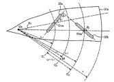
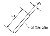
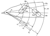
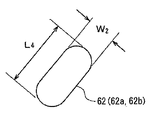
| KR20100122894A (ko) | 평면 안테나 부재, 및 이것을 구비한 플라즈마 처리 장치 | |
| WO2011013633A1 (ja) | 平面アンテナ部材およびこれを備えたプラズマ処理装置 | |
| JP5728565B2 (ja) | プラズマ処理装置及びこれに用いる遅波板 | |
| JP2013033979A (ja) | マイクロ波プラズマ処理装置 | |
| JP5066502B2 (ja) | プラズマ処理装置 | |
| JP2009099975A (ja) | プラズマ処理装置 |
Legal Events
| Date | Code | Title | Description |
|---|---|---|---|
| PA0105 | International application |
St.27 status event code: A-0-1-A10-A15-nap-PA0105 |
|
| PG1501 | Laying open of application |
St.27 status event code: A-1-1-Q10-Q12-nap-PG1501 |
|
| A201 | Request for examination | ||
| E13-X000 | Pre-grant limitation requested |
St.27 status event code: A-2-3-E10-E13-lim-X000 |
|
| P11-X000 | Amendment of application requested |
St.27 status event code: A-2-2-P10-P11-nap-X000 |
|
| P13-X000 | Application amended |
St.27 status event code: A-2-2-P10-P13-nap-X000 |
|
| PA0201 | Request for examination |
St.27 status event code: A-1-2-D10-D11-exm-PA0201 |
|
| E902 | Notification of reason for refusal | ||
| PE0902 | Notice of grounds for rejection |
St.27 status event code: A-1-2-D10-D21-exm-PE0902 |
|
| P11-X000 | Amendment of application requested |
St.27 status event code: A-2-2-P10-P11-nap-X000 |
|
| P13-X000 | Application amended |
St.27 status event code: A-2-2-P10-P13-nap-X000 |
|
| R17-X000 | Change to representative recorded |
St.27 status event code: A-3-3-R10-R17-oth-X000 |
|
| E90F | Notification of reason for final refusal | ||
| PE0902 | Notice of grounds for rejection |
St.27 status event code: A-1-2-D10-D21-exm-PE0902 |
|
| E601 | Decision to refuse application | ||
| PE0601 | Decision on rejection of patent |
St.27 status event code: N-2-6-B10-B15-exm-PE0601 |
|
| P22-X000 | Classification modified |
St.27 status event code: A-2-2-P10-P22-nap-X000 |