KR20100122894A - Flat antenna member and a plasma processing device provided with same - Google Patents
Flat antenna member and a plasma processing device provided with same Download PDFInfo
- Publication number
- KR20100122894A KR20100122894A KR1020107007491A KR20107007491A KR20100122894A KR 20100122894 A KR20100122894 A KR 20100122894A KR 1020107007491 A KR1020107007491 A KR 1020107007491A KR 20107007491 A KR20107007491 A KR 20107007491A KR 20100122894 A KR20100122894 A KR 20100122894A
- Authority
- KR
- South Korea
- Prior art keywords
- center
- planar antenna
- hole
- antenna member
- range
- Prior art date
Links
Images


Classifications
-
- H—ELECTRICITY
- H05—ELECTRIC TECHNIQUES NOT OTHERWISE PROVIDED FOR
- H05H—PLASMA TECHNIQUE; PRODUCTION OF ACCELERATED ELECTRICALLY-CHARGED PARTICLES OR OF NEUTRONS; PRODUCTION OR ACCELERATION OF NEUTRAL MOLECULAR OR ATOMIC BEAMS
- H05H1/00—Generating plasma; Handling plasma
- H05H1/24—Generating plasma
- H05H1/46—Generating plasma using applied electromagnetic fields, e.g. high frequency or microwave energy
-
- H—ELECTRICITY
- H01—ELECTRIC ELEMENTS
- H01J—ELECTRIC DISCHARGE TUBES OR DISCHARGE LAMPS
- H01J37/00—Discharge tubes with provision for introducing objects or material to be exposed to the discharge, e.g. for the purpose of examination or processing thereof
- H01J37/32—Gas-filled discharge tubes
- H01J37/32009—Arrangements for generation of plasma specially adapted for examination or treatment of objects, e.g. plasma sources
- H01J37/32192—Microwave generated discharge
- H01J37/32211—Means for coupling power to the plasma
- H01J37/3222—Antennas
Landscapes
- Physics & Mathematics (AREA)
- Engineering & Computer Science (AREA)
- Plasma & Fusion (AREA)
- Chemical & Material Sciences (AREA)
- Analytical Chemistry (AREA)
- Electromagnetism (AREA)
- Spectroscopy & Molecular Physics (AREA)
- Plasma Technology (AREA)
- Drying Of Semiconductors (AREA)
- Chemical Vapour Deposition (AREA)
Abstract
본 발명은 플라즈마 처리 장치의 처리 용기 내에 전자파 발생원에서 발생한 전자파를 도입하는 평면 안테나 부재로서, 도전성 재료로 이루어지는 평판형 기재와, 상기 평판형 기재에 형성된, 전자파를 방사하는 복수의 관통구를 구비하고, 상기 관통구는, 상기 평면 안테나 부재의 중심에 그 중심이 겹쳐지는 원의 둘레 상에 배열된 복수의 제1 관통구와, 상기 제1 관통구의 외측에 상기 원과 동심원 형상으로 배열된 복수의 제2 관통구를 포함하고 있으며, 상기 평면 안테나 부재의 중심으로부터 상기 제1 관통구의 중심까지의 거리(L1)와, 상기 평면 안테나 부재의 반경(r)의 비(L1/r)가, 0.35 ∼ 0.5의 범위이고, 상기 평면 안테나 부재의 중심으로부터 상기 제2 관통구의 중심까지의 거리(L2)와, 상기 평면 안테나 부재의 반경(r)의 비(L2/r)가, 0.7 ∼ 0.85의 범위인 것을 특징으로 하는 평면 안테나 부재이다.The present invention provides a planar antenna member for introducing electromagnetic waves generated from an electromagnetic wave generation source into a processing vessel of a plasma processing apparatus, comprising a flat substrate made of a conductive material and a plurality of through holes radiating electromagnetic waves formed on the flat substrate. The through holes may include a plurality of first through holes arranged on a circumference of a circle whose center overlaps with a center of the planar antenna member, and a plurality of second through holes arranged concentrically with the circle on an outer side of the first through hole. Including a through hole, the ratio L1 / r of the distance L1 from the center of the planar antenna member to the center of the first through hole and the radius r of the planar antenna member is 0.35 to 0.5. The distance L2 from the center of the planar antenna member to the center of the second through hole and the ratio L2 / r of the radius r of the planar antenna member are in the range of 0.7 to 0.85. To the planar antenna member, it characterized.
Description
본 발명은, 피처리체를 플라즈마 처리하는 처리 용기에 미리 정해진 주파수의 전자파를 유도하기 위해서 이용되는 평면 안테나 부재, 및 그 평면 안테나 부재를 구비한 플라즈마 처리 장치에 관한 것이다.BACKGROUND OF THE INVENTION 1. Field of the Invention The present invention relates to a planar antenna member used for inducing electromagnetic waves of a predetermined frequency in a processing vessel for plasma processing a target object, and a plasma processing apparatus including the planar antenna member.
반도체 웨이퍼 등의 피처리체에 대하여 산화 처리나 질화 처리 등의 플라즈마 처리를 행하는 플라즈마 처리 장치로서, 복수의 슬롯을 갖는 평면 안테나를 이용해서 처리 용기 내에 예컨대 주파수 2.45 ㎓의 마이크로파를 도입하여 플라즈마를 생성시키는 방식의 플라즈마 처리 장치가 알려져 있다(예컨대, 일본 특허 공개 평성 제11-260594호 공보, 일본 특허 공개 제2001-223171호 공보). 이러한 마이크로파 플라즈마 처리 장치에서는, 높은 플라즈마 밀도를 갖는 플라즈마를 생성시킴으로써, 챔버 내에서 표면파 플라즈마를 형성하는 것이 가능하다.A plasma processing apparatus for performing a plasma processing such as an oxidation process or a nitriding process on a target object such as a semiconductor wafer, wherein a plasma having a frequency of 2.45 kHz is introduced into a processing vessel using a planar antenna having a plurality of slots to generate plasma, for example. A plasma processing apparatus of the method is known (for example, Japanese Patent Laid-Open No. 11-260594 and Japanese Patent Laid-Open No. 2001-223171). In such a microwave plasma processing apparatus, it is possible to form a surface wave plasma in a chamber by generating a plasma having a high plasma density.
상술한 방식의 플라즈마 처리 장치에서는, 챔버 내의 압력을 높게 해 가면, 플라즈마 밀도가 저하되는 경향이 있다. 플라즈마 밀도가 낮아지면, 2.45 ㎓의 마이크로파의 각주파수(角周波數)보다도 플라즈마의 각주파수 쪽이 작아져 버려, 표면파 플라즈마를 안정적으로 유지할 수 없게 된다. 예컨대, 챔버 내 압력이 133.3 ㎩ 이상인 조건에서 플라즈마 처리를 행하는 경우, 플라즈마 밀도가 충분히 상승되지 않고, 표면파 플라즈마가 컷오프되어, 표면파 플라즈마가 아닌 통상의 벌크 플라즈마가 되어 버리는 경우가 있다.In the plasma processing apparatus of the system described above, when the pressure in the chamber is increased, the plasma density tends to be lowered. When the plasma density decreases, the angular frequency of the plasma becomes smaller than the angular frequency of the microwave of 2.45 GHz, and the surface wave plasma cannot be stably maintained. For example, when the plasma treatment is performed under a condition in which the pressure in the chamber is 133.3 Pa or more, the plasma density may not be sufficiently increased, and the surface wave plasma may be cut off to become a normal bulk plasma instead of the surface wave plasma.
차세대 이후의 디바이스 개발을 위해, 예컨대 3차원 디바이스 가공이나 미세화에 대한 대응을 도모하기 위해서는, 정밀한 처리가 가능한 비교적 높은 압력 조건하에서, 처리율의 향상이나 웨이퍼면 내에서의 처리의 균일성을 실현해 갈 필요가 있다. 이를 위해서는, 플라즈마의 제어성을 향상시켜, 플라즈마 밀도가 낮아지는 비교적 높은 압력 조건이라도, 컷오프가 없는 표면파 플라즈마를 안정적으로 유지할 수 있도록 할 필요가 있다. 표면파 플라즈마를 안정적으로 유지할 수 있도록 하기 위한 하나의 방책으로서, 전자파의 주파수를 낮추는 것이 고려된다. 예컨대, 주파수가 2.45 ㎓보다도 낮은 주파수의 전자파를 이용함으로써, 비교적 높은 압력 조건이라도 안정적으로 표면파 플라즈마를 유지할 수 있을 가능성이 있다.For the development of the devices after the next generation, for example, in order to cope with processing and miniaturization of three-dimensional devices, improvement of throughput and uniformity of processing in the wafer surface are realized under relatively high pressure conditions capable of precise processing. There is a need. For this purpose, it is necessary to improve the controllability of the plasma so that the surface wave plasma without cutoff can be stably maintained even under a relatively high pressure condition in which the plasma density becomes low. As one measure for stably maintaining the surface wave plasma, it is considered to lower the frequency of electromagnetic waves. For example, by using an electromagnetic wave whose frequency is lower than 2.45 kHz, there is a possibility that the surface wave plasma can be stably maintained even under relatively high pressure conditions.
그러나, 전자파를 효율적으로 챔버 내부로 유도하기 위한 평면 안테나의 구조(슬롯 패턴 등)는, 전자파의 주파수에 따라 상이하다. 종래 기술의 평면 안테나(슬롯 패턴 등)는, 주파수 2.45 ㎓의 마이크로파를 챔버 내에 도입할 목적으로 최적으로 배치 구성한 것이며, 종래의 마이크로파의 주파수보다도 낮은 예컨대 1 ㎓ 전후 정도의 주파수의 전자파에 적합한 평면 안테나에 관한 구조면(슬롯 패턴)의 검토는 충분히 이루어져 있지 않다. 애당초, 1 ㎓ 이하의 비교적 낮은 주파수의 전자파를 사용하는 플라즈마 처리 장치에는, 표면파 플라즈마의 생성이 어렵기 때문에, 평면 안테나 자체가 사용되고 있지 않았다는 사정이 있다.However, the structure (slot pattern, etc.) of the planar antenna for efficiently inducing electromagnetic waves into the chamber varies depending on the frequency of the electromagnetic waves. Conventional planar antennas (slot patterns, etc.) are optimally arranged and configured for the purpose of introducing microwaves with a frequency of 2.45 GHz into the chamber, and are suitable for electromagnetic waves having a frequency of about 1 kHz or less, which is lower than that of conventional microwaves. Examination of the structural surface (slot pattern) concerning is not made enough. Initially, since the surface wave plasma is difficult to generate in the plasma processing apparatus using a relatively low frequency electromagnetic wave of 1 kHz or less, there is a situation that the planar antenna itself is not used.
일반적으로, 전자파의 주파수를 낮추면, 그 파장이 길어진다. 이러한 점에서, 2.45 ㎓의 주파수의 마이크로파를 유도하는 경우에 비하여, 1 ㎓ 정도의 주파수의 전자파를 유도하는 경우에는, 평면 안테나의 슬롯의 길이나 슬롯의 간격을 크게 하는 것이 고려된다. 그러나, 이론적으로 계산된 슬롯의 길이나 배치에 기초하여 제작된 평면 안테나를 이용해서 플라즈마를 형성해도, 안정적으로 표면파 플라즈마를 형성할 수 있다고는 할 수 없다. 예컨대, 최근에는, 300 ㎜ 웨이퍼의 처리에 대응할 수 있도록 플라즈마 처리 장치가 대형화되어 있고, 450 ㎜ 웨이퍼에 대한 대응도 요구되고 있다. 이에 따라, 평면 안테나도 대직경화되고 있다. 예컨대 300 ㎜ 웨이퍼를 처리하기 위한 평면 안테나는, 직경이 500 ㎜ 부근에도 이른다. 450 ㎜ 웨이퍼의 경우에는, 평면 안테나가 더 대형화되어, 직경이 600 ㎜ ∼ 700 ㎜ 정도에나 이른다. 이와 같이 대형의 평면 안테나에서는, 슬롯의 길이나 배치를 계산상 얻어지는 최적값으로 설정하더라도, 실제 장치에서 행해도, 안정적으로 표면파 플라즈마를 유지하는 것은 곤란하다.In general, the lower the frequency of the electromagnetic wave, the longer the wavelength. In this regard, when inducing electromagnetic waves with a frequency of about 1 kHz as compared with the case of inducing microwaves with a frequency of 2.45 kHz, it is considered to increase the slot length and slot spacing of the planar antenna. However, even if the plasma is formed using a planar antenna manufactured based on the theoretically calculated slot length or arrangement, the surface wave plasma cannot be stably formed. For example, in recent years, the plasma processing apparatus has been enlarged to cope with the processing of a 300 mm wafer, and a response to the 450 mm wafer is also required. As a result, the planar antenna is also large diameter. For example, a flat antenna for processing a 300 mm wafer reaches around 500 mm in diameter. In the case of a 450 mm wafer, the planar antenna is further enlarged, and the diameter is only about 600 mm to 700 mm. In such a large planar antenna, it is difficult to stably maintain the surface wave plasma even if the length or arrangement of slots is set to an optimal value obtained by calculation or performed in an actual apparatus.
본 발명은, 상기 실정을 감안하여 이루어진 것으로, 그 제1 목적은, 종래의 마이크로파의 주파수보다도 낮은 주파수의 전자파를 챔버 내에 효율적으로 도입할 수 있는 평면 안테나를 제공하는 것이다. 또한, 본 발명의 제2 목적은, 종래의 마이크로파의 주파수보다도 낮은 주파수의 전자파를 이용하고, 대형의 기판을 처리하는 경우라도, 플라즈마의 제어성이 높아, 챔버 내에서 안정적으로 표면파 플라즈마를 형성할 수 있는 플라즈마 처리 장치를 제공하는 것이다.This invention is made | formed in view of the said situation, The 1st objective is to provide the planar antenna which can introduce | transduce the electromagnetic wave of the frequency lower than the frequency of the conventional microwave in a chamber efficiently. Further, the second object of the present invention is to control surface plasma even in the case of processing a large substrate by using electromagnetic waves having a frequency lower than that of conventional microwaves, so that surface wave plasma can be stably formed in the chamber. It is to provide a plasma processing apparatus.
본 발명은, 플라즈마 처리 장치의 처리 용기 내에 전자파 발생원에서 발생한 전자파를 도입하는 평면 안테나 부재로서, 도전성 재료로 이루어지는 평판형 기재(基材)와, 상기 평판형 기재에 형성된, 전자파를 방사하는 복수의 관통구를 구비하고, 상기 관통구는, 상기 평면 안테나 부재의 중심에 그 중심이 겹쳐지는 원의 둘레 상에 배열된 복수의 제1 관통구와, 상기 제1 관통구의 외측에 상기 원과 동심원 형상으로 배열된 복수의 제2 관통구를 포함하고 있으며, 상기 평면 안테나 부재의 중심으로부터 상기 제1 관통구의 중심까지의 거리(L1)와, 상기 평면 안테나 부재의 반경(r)의 비(L1/r)가, 0.35 ∼ 0.5의 범위이고, 상기 평면 안테나 부재의 중심으로부터 상기 제2 관통구의 중심까지의 거리(L2)와, 상기 평면 안테나 부재의 반경(r)의 비(L2/r)가, 0.7 ∼ 0.85의 범위인 것을 특징으로 하는 평면 안테나 부재이다.The present invention provides a planar antenna member for introducing electromagnetic waves generated from an electromagnetic wave generating source into a processing container of a plasma processing apparatus, comprising: a flat substrate made of a conductive material and a plurality of radiating electromagnetic waves formed on the flat substrate. A through-hole, the through-holes being arranged on a circumference of a circle in which the center overlaps the center of the planar antenna member, and arranged in a concentric shape with the circle on the outside of the first through-hole. And a plurality of second through holes, wherein the ratio L1 from the center of the planar antenna member to the center of the first through hole and the radius L of the planar antenna member L1 / r , 0.35 to 0.5, and the ratio L2 / r of the distance L2 from the center of the planar antenna member to the center of the second through hole and the radius r of the planar antenna member is 0.7 to 0.85. Offense It is a flat antenna member characterized in that the above.
본 발명에 따른 평면 안테나 부재에 따르면, 평면 안테나 부재의 중심으로부터 제1 관통구의 중심까지의 거리(L1)와 평면 안테나 부재의 반경(r)의 비(L1/r)를 0.35 ∼ 0.5의 범위로 하고, 평면 안테나 부재의 중심으로부터 제2 관통구의 중심까지의 거리(L2)와 평면 안테나 부재의 반경(r)의 비(L2/r)를 0.7 ∼ 0.85의 범위로 함으로써, 전자파 발생 장치에서 발생되는 전자파의 주파수를 종래의 마이크로파의 주파수보다 낮은 800 ㎒ ∼ 1000 ㎒로 한 경우라도, 반사파의 발생을 억제할 수 있고, 그 전자파를 챔버 내에 효율적으로 도입할 수 있다. 따라서, 챔버 내에서 표면파 플라즈마를 안정적으로 유지할 수 있고, 기판의 대형화에 대한 대응도 가능해진다.According to the planar antenna member according to the present invention, the ratio L1 / r of the distance L1 from the center of the planar antenna member to the center of the first through hole and the radius r of the planar antenna member is in the range of 0.35 to 0.5. The ratio L2 / r of the distance L2 from the center of the planar antenna member to the center of the second through hole and the radius r of the planar antenna member is in the range of 0.7 to 0.85, thereby generating the electromagnetic wave generating device. Even when the frequency of electromagnetic waves is set to 800 MHz to 1000 MHz, which is lower than that of conventional microwaves, generation of reflected waves can be suppressed, and the electromagnetic waves can be efficiently introduced into the chamber. Therefore, the surface wave plasma can be stably maintained in the chamber, and it is possible to cope with the enlargement of the substrate.
상기 거리(L1)를 반경으로 하고 상기 제1 관통구의 중심을 지나는 제1 원과, 상기 거리(L2)를 반경으로 하고 상기 제2 관통구의 중심을 지나는 제2 원에 대하여 동심원 형상이며, 그 제1 원의 원주와 그 제2 원의 원주 사이의 직경 방향의 중간점을 지나는 제3 원에 대해서, 그 반경(L3)과 상기 반경(r)의 비(L3/r)가, 0.5 ∼ 0.7의 범위인 것이 바람직하다.A first circle passing through the center of the first through hole with the radius L1 as the radius, and a second circle passing through the center of the second through hole with the radius L2 as the radius and being concentric in shape. For the third circle passing through the radial midpoint between the circumference of one circle and the circumference of the second circle, the ratio L3 / r of the radius L3 and the radius r is 0.5 to 0.7. It is preferable that it is a range.
또한, 상기 거리(L2) 및 상기 거리(L1)의 차분(L2-L1)과 상기 평면 안테나 부재의 반경(r)의 비[(L2-L1)/r]가, 0.2 ∼ 0.5의 범위인 것이 바람직하다.Further, the ratio [(L2-L1) / r] of the difference L2-L1 between the distance L2 and the distance L1 and the radius r of the planar antenna member is in the range of 0.2 to 0.5. desirable.
또한, 상기 제1 관통구 및 상기 제2 관통구는, 모두 가늘고 긴 형상이고, 상기 제1 관통구의 길이 방향에 대하여, 상기 제2 관통구의 길이 방향이 이루는 각도는, 85°∼ 95°의 범위인 것이 바람직하다. 이 경우, 또한, 상기 평면 안테나 부재의 중심과 상기 제1 관통구의 중심을 연결하는 직선에 대하여, 그 제1 관통구의 길이 방향이 이루는 각도는, 30°∼ 50°의 범위인 것이 바람직하다. 또한, 상기 평면 안테나 부재의 중심과 상기 제2 관통구의 중심을 연결하는 직선에 대하여, 그 제2 관통구의 길이 방향이 이루는 각도는, 130°∼ 150°의 범위인 것이 바람직하다.The first through hole and the second through hole are both elongated in shape, and the angle formed by the longitudinal direction of the second through hole with respect to the longitudinal direction of the first through hole is in a range of 85 ° to 95 °. It is preferable. In this case, the angle formed by the longitudinal direction of the first through hole with respect to a straight line connecting the center of the planar antenna member and the center of the first through hole is preferably in the range of 30 ° to 50 °. Moreover, it is preferable that the angle which the longitudinal direction of the 2nd through hole makes with respect to the straight line which connects the center of the said planar antenna member and the center of the said 2nd through hole is 130 to 150 degree.
또한, 상기 평면 안테나 부재의 중심으로부터 상기 제1 관통구의 중심까지를 연결하는 직선과, 상기 평면 안테나 부재의 중심으로부터 상기 제2 관통구의 중심까지를 연결하는 직선이 이루는 각도가, 8°∼ 15°의 범위인 것이 바람직하다.The angle formed by a straight line connecting the center of the planar antenna member to the center of the first through hole and a straight line connecting the center of the planar antenna member to the center of the second through hole is 8 ° to 15 °. It is preferable that it is the range of.
또한, 상기 전자파 발생원에서 발생되는 전자파의 주파수는, 800 ㎒ ∼ 1000 ㎒의 범위인 것이 바람직하다.Moreover, it is preferable that the frequency of the electromagnetic wave generate | occur | produced in the said electromagnetic wave generating source is the range of 800 MHz-1000 MHz.
또는, 본 발명은, 피처리체를 수용하는 탈기 가능한 처리 용기와, 상기 처리 용기 내에 가스를 공급하는 가스 도입부와, 상기 처리 용기 내부를 감압 배기하는 배기 장치와, 상기 처리 용기의 상부의 개구부에 기밀하게 장착되고, 상기 처리 용기 내에 플라즈마를 생성하기 위한 전자파를 투과시키는 투과판과, 상기 투과판 위에 배치되고, 상기 전자파를 상기 처리 용기 내에 도입하는 평면 안테나 부재와, 상기 평면 안테나 부재를 상방으로부터 덮는 커버 부재와, 상기 커버 부재를 관통하여 설치되고, 전자파 발생원에서 발생된 800 ㎒ ∼ 1000 ㎒의 범위의 전자파를 상기 평면 안테나 부재에 공급하는 도파관을 구비하며, 상기 평면 안테나 부재는, 도전성 재료로 이루어지는 평판형 기재와, 상기 평판형 기재에 형성된, 전자파를 방사하는 복수의 관통구를 가지며, 상기 관통구는, 원형 형상으로 배열된 복수의 제1 관통구와, 상기 제1 관통구의 외측에 동심원 형상으로 배열된 복수의 제2 관통구를 포함하며, 상기 평면 안테나 부재의 중심으로부터 상기 제1 관통구의 중심까지의 거리(L1)와, 상기 평면 안테나 부재의 반경(r)의 비(L1/r)가, 0.35 ∼ 0.5의 범위이고, 상기 평면 안테나 부재의 중심으로부터 상기 제2 관통구의 중심까지의 거리(L2)와, 상기 평면 안테나 부재의 반경(r)의 비(L2/r)가, 0.7 ∼ 0.85의 범위인 것을 특징으로 하는 플라즈마 처리 장치이다.Alternatively, the present invention provides a gas-tight process container for receiving a target object, a gas inlet for supplying gas into the processing container, an exhaust device for evacuating the inside of the processing container under reduced pressure, and an airtight opening in an upper portion of the processing container. And a transmissive plate for transmitting electromagnetic waves for generating plasma in the processing container, a planar antenna member disposed on the transmissive plate and introducing the electromagnetic wave into the processing container, and covering the planar antenna member from above. A cover member and a waveguide provided through the cover member and supplying electromagnetic waves in the range of 800 MHz to 1000 MHz generated from an electromagnetic wave source to the planar antenna member, wherein the planar antenna member is made of a conductive material. A flat substrate and a plurality of through holes for emitting electromagnetic waves formed in the flat substrate The through-hole includes a plurality of first through-holes arranged in a circular shape, and a plurality of second through-holes arranged concentrically on the outer side of the first through-hole, wherein the first through-hole is formed from the center of the planar antenna member. The ratio L1 / r of the distance L1 to the center of the through hole and the radius r of the planar antenna member is in the range of 0.35 to 0.5, from the center of the planar antenna member to the center of the second through hole. The ratio L2 / r between the distance L2 and the radius r of the planar antenna member is in the range of 0.7 to 0.85.
본 발명에 따른 플라즈마 처리 장치에 따르면, 전자파 발생원에서 발생되는 전자파의 주파수를 종래의 마이크로파의 주파수보다 낮은 800 ㎒ ∼ 1000 ㎒의 범위로 설정함으로써, 예컨대 2.45 ㎓의 마이크로파를 사용하는 경우와 비교하여, 보다 높은 압력 범위까지 컷오프 밀도 이상의 플라즈마 밀도를 유지할 수 있다. 따라서, 본 발명에 따른 플라즈마 처리 장치에 따르면, 비교적 높은 압력 조건이라도, 충분한 처리율이나 웨이퍼면 내에서의 처리의 균일성을 확보할 수 있고, 높은 정밀도가 필요한 3차원 디바이스의 가공이나 미세 가공에 대한 대응도 가능해진다.According to the plasma processing apparatus according to the present invention, by setting the frequency of the electromagnetic wave generated from the electromagnetic wave generating source in the range of 800 MHz to 1000 MHz, which is lower than the frequency of the conventional microwave, for example, when using a microwave of 2.45 GHz, A plasma density above the cutoff density can be maintained up to a higher pressure range. Therefore, according to the plasma processing apparatus according to the present invention, even in a relatively high pressure condition, a sufficient throughput and uniformity of processing in the wafer surface can be ensured, and the processing and fine processing of a three-dimensional device requiring high precision can be achieved. Correspondence becomes possible, too.
본 발명에서도, 상기 거리(L1)를 반경으로 하고 상기 제1 관통구의 중심을 지나는 제1 원과, 상기 거리(L2)를 반경으로 하고 상기 제2 관통구의 중심을 지나는 제2 원에 대하여 동심원 형상이며, 그 제1 원의 원주와 그 제2 원의 원주 사이의 직경 방향의 중간점을 지나는 제3 원에 대해서, 그 반경(L3)과 상기 반경(r)의 비(L3/r)가, 0.5 ∼ 0.7의 범위인 것이 바람직하다.Also in the present invention, a first circle passing through the center of the first through hole with the radius L1 as a radius and a second circle passing through the center of the second through hole with the radius L2 as the radius are concentric. The ratio L3 / r of the radius L3 and the radius r is about the third circle passing through the midpoint of the radial direction between the circumference of the first circle and the circumference of the second circle. It is preferable that it is the range of 0.5-0.7.
또한, 상기 거리(L2) 및 상기 거리(L1)의 차분(L2-L1)과 상기 평면 안테나 부재의 반경(r)의 비[(L2-L1)/r]가, 0.2 ∼ 0.5의 범위인 것이 바람직하다.Further, the ratio [(L2-L1) / r] of the difference L2-L1 between the distance L2 and the distance L1 and the radius r of the planar antenna member is in the range of 0.2 to 0.5. desirable.
또한, 상기 제1 관통구 및 상기 제2 관통구는, 모두 가늘고 긴 형상이고, 상기 제1 관통구의 길이 방향에 대하여, 상기 제2 관통구의 길이 방향이 이루는 각도는, 85°∼ 95°의 범위인 것이 바람직하다. 이 경우, 또한, 상기 평면 안테나 부재의 중심과 상기 제1 관통구의 중심을 연결하는 직선에 대하여, 그 제1 관통구의 길이 방향이 이루는 각도는, 30°∼ 50°의 범위인 것이 바람직하다. 또한, 상기 평면 안테나 부재의 중심과 상기 제2 관통구의 중심을 연결하는 직선에 대하여, 그 제2 관통구의 길이 방향이 이루는 각도는, 130°∼ 150°의 범위인 것이 바람직하다.The first through hole and the second through hole are both elongated in shape, and the angle formed by the longitudinal direction of the second through hole with respect to the longitudinal direction of the first through hole is in a range of 85 ° to 95 °. It is preferable. In this case, the angle formed by the longitudinal direction of the first through hole with respect to a straight line connecting the center of the planar antenna member and the center of the first through hole is preferably in the range of 30 ° to 50 °. Moreover, it is preferable that the angle which the longitudinal direction of the 2nd through hole makes with respect to the straight line which connects the center of the said planar antenna member and the center of the said 2nd through hole is 130 to 150 degree.
또한, 상기 평면 안테나 부재의 중심으로부터 상기 제1 관통구의 중심까지를 연결하는 직선과, 상기 평면 안테나 부재의 중심으로부터 상기 제2 관통구의 중심까지를 연결하는 직선이 이루는 각도가, 8°∼ 15°의 범위인 것이 바람직하다.The angle formed by a straight line connecting the center of the planar antenna member to the center of the first through hole and a straight line connecting the center of the planar antenna member to the center of the second through hole is 8 ° to 15 °. It is preferable that it is the range of.
본 발명에 의하면, 종래의 마이크로파의 주파수보다도 낮은 주파수의 전자파를 챔버 내에 효율적으로 도입할 수 있는 평면 안테나를 제공할 수 있고, 종래의 마이크로파의 주파수보다도 낮은 주파수의 전자파를 이용하고, 대형의 기판을 처리하는 경우라도, 플라즈마의 제어성이 높아, 챔버 내에서 안정적으로 표면파 플라즈마를 형성할 수 있는 플라즈마 처리 장치를 제공할 수 있다.According to the present invention, it is possible to provide a planar antenna capable of efficiently introducing an electromagnetic wave having a frequency lower than that of a conventional microwave into a chamber, and using an electromagnetic wave of a frequency lower than that of a conventional microwave, Even in the case of processing, a plasma processing apparatus capable of forming surface wave plasma stably in a chamber can be provided with high controllability of plasma.
도 1은 본 발명의 제1 실시형태에 따른 플라즈마 처리 장치를 도시하는 개략 단면도이다.
도 2는 본 발명의 제1 실시형태에 따른 평면 안테나판의 주요부의 평면도이다.
도 3은 도 2의 평면 안테나판에서의 슬롯의 확대도이다.
도 4는 도 1의 플라즈마 처리 장치의 제어 계통의 개략 구성을 도시하는 블록도이다.
도 5는 플라즈마의 컷오프 밀도의 압력 의존 모델을 설명하기 위한 그래프이다.
도 6은 본 발명의 제2 실시형태에 따른 평면 안테나판의 주요부의 평면도이다.
도 7은 도 6의 평면 안테나판에서의 슬롯의 확대도이다.
도 8은 본 발명의 제3 실시형태에 따른 평면 안테나판의 주요부의 평면도이다.1 is a schematic cross-sectional view showing a plasma processing apparatus according to a first embodiment of the present invention.
2 is a plan view of an essential part of the planar antenna plate according to the first embodiment of the present invention.
3 is an enlarged view of a slot in the planar antenna plate of FIG. 2.
4 is a block diagram illustrating a schematic configuration of a control system of the plasma processing apparatus of FIG. 1.
5 is a graph for explaining a pressure dependent model of the cutoff density of plasma.
6 is a plan view of an essential part of the planar antenna plate according to the second embodiment of the present invention.
FIG. 7 is an enlarged view of a slot in the planar antenna plate of FIG. 6.
8 is a plan view of an essential part of the planar antenna plate according to the third embodiment of the present invention.
[제1 실시형태][First Embodiment]
이하, 본 발명의 실시형태에 대해서, 도면을 참조하여 상세히 설명한다. 도 1은 본 발명의 제1 실시형태에 따른 플라즈마 처리 장치(100)의 개략 구성을 모식적으로 도시하는 단면도이다. 또한, 도 2는 도 1의 플라즈마 처리 장치(100)에 이용된, 본 발명의 제1 실시형태에 따른 평면 안테나판(평면 안테나 부재)을 도시하는 주요부 평면도이고, 도 3은 그 평면 안테나판에서의 관통구로서의 슬롯의 확대도이다. 또한, 도 4는 도 1의 플라즈마 처리 장치(100)에서의 제어 계통의 개략 구성의 일례를 도시하는 블록도이다.EMBODIMENT OF THE INVENTION Hereinafter, embodiment of this invention is described in detail with reference to drawings. FIG. 1: is sectional drawing which shows schematic structure of the
플라즈마 처리 장치(100)는, 복수의 슬롯 형상의 관통구(구멍)를 갖는 평면 안테나판, 특히 RLSA(Radial Line Slot Antenna; 레이디얼 라인 슬롯 안테나)에 의해 처리 용기 내에 전자파를 도입하여 플라즈마를 발생시킴으로써, 고밀도이며 저전자 온도의 플라즈마를 발생시키는 플라즈마 처리 장치로서 구성된다. 플라즈마 처리 장치(100)에서는, 1010/㎤ ∼ 1013/㎤의 플라즈마 밀도이고, 0.5 eV ∼ 2 eV 이하의 저전자 온도를 갖는 플라즈마에 의한 처리를 할 수 있다. 따라서, 플라즈마 처리 장치(100)는, 각종 반도체 장치의 제조 과정에서 적합하게 이용할 수 있다.The
플라즈마 처리 장치(100)는, 주요한 구성으로서, 기밀하게 구성된 챔버(처리 용기)(1)와, 챔버(1) 내에 가스를 공급하는 가스 공급부(18)와, 챔버(1) 내부를 감압 배기하기 위한 배기 장치(24)와, 챔버(1)의 상부에 형성되어 챔버(1) 내에 전자파를 도입하는 전자파 도입부(27)와, 평면 안테나판(31)과, 이들 플라즈마 처리 장치(100)의 각 구성부를 제어하는 제어부(50)를 구비한다. 또한, 가스 공급부(18), 배기 장치(24) 및 전자파 도입부(27)는, 챔버(1) 내에서 플라즈마를 생성시키는 플라즈마 생성 수단을 구성한다.As a main configuration, the
챔버(1)는, 접지된 대략 원통 형상의 용기에 의해 형성된다. 또한, 챔버(1)는, 각통(角筒) 형상의 용기에 의해 형성되어도 된다. 챔버(1)는, 알루미늄 등의 금속 재질로 이루어지는 바닥벽(1a)과 측벽(1b)을 갖는다.The chamber 1 is formed of a substantially cylindrical container grounded. In addition, the chamber 1 may be formed of a rectangular cylinder. The chamber 1 has the
챔버(1)의 내부에는, 피처리체인 실리콘 웨이퍼(이하, 간단히 「웨이퍼」라고 기재함)(W)를 수평으로 지지하기 위한 배치대(2)가 설치된다. 배치대(2)는, 열전도성이 높은 재질, 예컨대 AlN 등의 세라믹스에 의해 구성된다. 이 배치대(2)는, 배기실(11)의 바닥부 중앙으로부터 상방으로 연장되는 원통형의 지지 부재(3)에 의해 지지된다. 지지 부재(3)는, 예컨대 AlN 등의 세라믹스에 의해 구성된다.In the chamber 1, a mounting table 2 for horizontally supporting a silicon wafer (hereinafter simply referred to as "wafer") W as an object to be processed is provided. The mounting table 2 is made of a material having high thermal conductivity, for example, ceramics such as AlN. This mounting table 2 is supported by a cylindrical support member 3 extending upward from the bottom center of the
또한, 배치대(2)에는, 그 외측 가장자리부를 커버하며, 웨이퍼(W)를 가이드하기 위한 커버 링(4)이 설치된다. 이 커버 링(4)은, 예컨대 석영, AlN, Al2O3, SiN 등의 재질로 구성된 환형 부재이다. 단, 커버 링(4)은, 배치대(2)의 표면 전체면을 덮도록 배치되어도 된다.In addition, the mounting table 2 is provided with a cover ring 4 for covering the outer edge portion and for guiding the wafer W. As shown in FIG. The cover ring 4 is an annular member made of a material such as quartz, AlN, Al 2 O 3 , SiN, or the like. However, the cover ring 4 may be arrange | positioned so that the whole surface of the surface of the mounting table 2 may be covered.
또한, 배치대(2)에는, 온도 조절 기구로서의 저항 가열형 히터(5)가 매립되어 있다. 이 히터(5)는, 히터 전원(5a)으로부터 급전됨으로써, 배치대(2)를 가열하고, 그 열에 의해 피처리 기판인 웨이퍼(W)를 균일하게 가열하도록 되어 있다.Moreover, the
또한, 배치대(2)에는, 열전대(TC)(6)가 배치된다. 이 열전대(6)에 의해 온도를 계측함으로써, 웨이퍼(W)의 가열 온도를 예컨대 실온으로부터 900℃까지의 범위에서 제어할 수 있게 되어 있다.In addition, a thermocouple (TC) 6 is disposed on the mounting table 2. By measuring the temperature with this
또한, 배치대(2)에는, 웨이퍼(W)를 지지하여 승강시키기 위한 웨이퍼 지지핀(도시하지 않음)이 설치된다. 각 웨이퍼 지지핀은, 배치대(2)의 표면에 대하여 돌출되거나 들어갈 수 있도록 설치된다.In addition, the mounting table 2 is provided with a wafer support pin (not shown) for supporting and lifting the wafer W. As shown in FIG. Each wafer support pin is provided to protrude or enter the surface of the mounting table 2.
챔버(1)의 내주에는, 석영으로 이루어지는 원통형의 라이너(7)가 설치된다. 또한, 배치대(2)의 외주측에는, 챔버(1) 내부를 균일하게 배기하기 위해서, 다수의 배기 구멍(8a)을 갖는 석영제의 배플 플레이트(8)가 환형으로 설치되어 있다. 이 배플 플레이트(8)는, 복수의 지주(9)에 의해 지지된다. 또한, 플라즈마 처리 장치(100)를 플라즈마 CVD 장치로서 사용하는 경우에는, 라이너(7) 및 배플 플레이트(8)는 배치하지 않아도 된다.At the inner circumference of the chamber 1, a
챔버(1)의 바닥벽(1a)의 대략 중앙부에는, 챔버(1) 내의 분위기를 배출하는 개구부(10)가 형성된다. 이 개구부(10)를 덮도록 연통되고 하방을 향하여 돌출되는 배기실(11)이 형성된다. 이 배기실(11)에는, 배기관(12)이 접속되어 있고, 그 배기관(12)에 배기 장치(24)가 접속되어 있어, 챔버(1) 내부를 균등하게 배기할 수 있도록 되어 있다.The
챔버(1)의 상부의 개구부에는, 챔버(1)를 개폐시키는 환형의 덮개 프레임(리드)(13)이 배치된다. 덮개 프레임(13)의 내주부는, 내측(챔버 내 공간)을 향하여 돌출되며, 투과판(28)을 지지하는 환형의 지지부(13a)를 형성한다.In the opening part of the upper part of the chamber 1, the annular cover frame (lead) 13 which opens and closes the chamber 1 is arrange | positioned. The inner circumferential portion of the
챔버(1)의 상부[측벽(1b)]에는, 가스 도입부(15)가 형성된다. 이 가스 도입부(15)는, 처리 가스(산소 함유 가스나 플라즈마 여기용 가스)를 공급하는 가스 공급부(18)에 가스 배관을 통해 접속되어 있다. 또한, 가스 도입부(15)는, 챔버(1) 내부로 돌출되는 노즐 형상, 또는 복수의 가스 구멍을 갖는 샤워 형상으로 형성해도 된다.In the upper part (
또한, 챔버(1)의 측벽(1b)에는, 플라즈마 처리 장치(100)와 이것에 인접하는 반송실(도시하지 않음) 사이에서 웨이퍼(W)를 반입출하기 위한 반입출구(16)와, 이 반입출구(16)를 개폐하는 게이트 밸브(17)가 설치된다.The
가스 공급부(18)는, 예컨대, 플라즈마 여기용 Ar, Kr, Xe, He 등의 희가스나, 산화 처리에서의 산소 함유 가스 등의 산화성 가스, 질화 처리에서의 질소 함유 가스, 성막(成膜)용 가스 등의 처리 가스 등을 공급하는 가스 공급원(도시하지 않음)을 갖는다. 또한, CVD 처리의 경우에는, 원료 가스, 챔버 내 분위기를 치환할 때에 이용하는 N2, Ar 등의 퍼지 가스, 챔버(1) 내부를 클리닝할 때에 이용하는 ClF3, NF3 등의 클리닝 가스 등을 공급하는 가스 공급원을 설치할 수도 있다. 각 가스 공급원은, 도시하지 않은 매스 플로우 컨트롤러 및 개폐 밸브를 구비하여, 공급되는 가스의 전환이나 유량 등을 제어할 수 있도록 되어 있다.The
배기 장치(24)는, 예컨대 터보 분자 펌프 등의 고속 진공 펌프를 구비한다. 상술한 바와 같이, 배기 장치(24)는, 배기관(12)을 통해 챔버(1)의 배기실(11)에 접속된다. 배기 장치(24)를 작동시킴으로써, 챔버(1) 내의 가스는, 배기실(11)의 공간(11a) 내부로 균일하게 흐르고, 또한 공간(11a)으로부터 배기관(12)을 통해 외부로 배기된다. 이에 따라, 챔버(1) 내부를 예컨대 0.133 ㎩까지 고속으로 감압할 수 있게 되어 있다.The exhaust device 24 includes, for example, a high speed vacuum pump such as a turbo molecular pump. As described above, the exhaust device 24 is connected to the
다음으로, 전자파 도입부(27)의 구성에 대해서 설명한다. 전자파 도입부(27)는, 주요한 구성으로서, 투과판(28), 평면 안테나판(31), 지파판(遲波板;33), 커버 부재(34), 도파관(37), 매칭 회로(38) 및 전자파 발생 장치(39)를 구비한다.Next, the structure of the electromagnetic
전자파를 투과시키는 투과판(28)은, 덮개 프레임(13)에 있어서 내주측으로 돌출된 지지부(13a) 상에 배치되어 있다. 투과판(28)은, 유전체, 예컨대 석영이나 Al2O3, AlN 등의 세라믹스로 구성된다. 이 투과판(28)과 지지부(13a) 사이는, 밀봉 부재(29)를 통해 기밀하게 밀봉되어 있다. 따라서, 챔버(1) 내부는 기밀하게 유지된다.The
평면 안테나판(31)은, 투과판(28)의 상방에 있어서, 배치대(2)와 대향하도록 설치된다. 평면 안테나판(31)은, 원판 형상을 이루고 있다. 또한, 평면 안테나판(31)의 형상은, 원판 형상에 한정되지 않고, 예컨대 사각판 형상이어도 된다. 이 평면 안테나판(31)은, 덮개 프레임(13)의 상단에 결합되어 접지된다.The
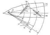
평면 안테나판(31)은, 예컨대 도 2 및 도 3에 도시하는 바와 같이, 원판형의 기재(31a)와, 이 기재(31a)에 미리 정해진 패턴으로 관통 형성된 쌍을 이루는 다수의 슬롯[32(32a, 32b)]을 갖는다. 기재(31a)는, 예컨대 표면이 금 또는 은 도금된 구리판, 알루미늄판, 니켈판 등의 도체판에 의해 구성된다. 전자파 방사 구멍으로서 기능하는 개개의 슬롯(32)은, 가늘고 긴 형상을 이루고 있으나, 슬롯(32)의 코너부에서는, 전계가 집중되어, 이상 방전을 일으키기 쉬워진다. 이 때문에, 가늘고 긴 슬롯(32)의 양단의 코너부는, 둥그스름한 형상으로 가공되어 있다. 또한, 슬롯(32)은, 평면 안테나판(31)의 중심(OA)측 위치에, 중심(OA)과 겹쳐지는 중심을 갖는 원의 둘레 상에 둘레 방향으로 배열된 복수의 제1 슬롯(32a)과, 이들 제1 슬롯(32a)을 둘러싸도록 외측에 배열된 복수의 제2 슬롯(32b)을 포함하고 있다. 제1 슬롯(32a)과 제2 슬롯(32b)은, 쌍을 이루어 동심원 형상으로 배열된다. 평면 안테나판(31)에서의 슬롯(32)의 배치에 대해서는, 이후에 상세히 기술한다.As shown in Figs. 2 and 3, the
평면 안테나판(31) 위에는, 진공보다도 큰 유전율을 갖는 재료로 이루어지는 지파판(33)이 설치된다. 지파판(33)은, 평면 안테나판(31)을 덮도록 배치된다. 지파판(33)의 재료로서는, 예컨대, 석영, 폴리테트라플루오로에틸렌 수지, 폴리이미드 수지 등을 들 수 있다. 이 지파판(33)은, 진공 중에서 전자파의 파장이 길어지는 것을 고려하여, 전자파의 파장을 짧게 해서 플라즈마를 조정하는 기능을 갖고 있다.On the
또한, 평면 안테나판(31)과 투과판(28) 사이, 또한, 지파판(33)과 평면 안테나판(31) 사이는, 각각 접촉시켜도 되고 이격시켜도 되지만, 정재파의 발생을 억제하는 관점에서는, 접촉시키는 것이 바람직하다.In addition, although the
챔버(1)의 상부에는, 평면 안테나판(31) 및 지파판(33)을 덮도록, 도파로를 형성하는 기능도 갖는 도체로 이루어지는 커버 부재(34)가 설치된다. 커버 부재(34)는, 예컨대 알루미늄이나 스테인리스강, 구리 등의 금속 재료의 도체에 의해 형성된다. 덮개 프레임(13)의 상단과 커버 부재(34)는, 전자파가 외부로 누설되지 않도록, 도전성을 갖는 스파이럴 실드 링 등의 밀봉 부재(35)에 의해 밀봉된다. 또한, 커버 부재(34)에는, 냉각수 유로(34a)가 형성된다. 이 냉각수 유로(34a)에 냉각수를 통류시킴으로써, 커버 부재(34), 지파판(33), 평면 안테나판(31), 투과판(28) 및 덮개 프레임(13)을 냉각할 수 있도록 되어 있다. 이 냉각 기구에 의해, 커버 부재(34), 지파판(33), 평면 안테나판(31), 투과판(28) 및 덮개 프레임(13)이, 플라즈마의 열에 의해 변형·파손되는 것이 방지된다. 또한, 덮개 프레임(13), 평면 안테나판(31) 및 커버 부재(34)는 접지된다.In the upper part of the chamber 1, the
커버 부재(34)의 상벽(천장부)의 중앙에는, 개구부(36)가 형성되어 있고, 이 개구부(36)에 도파관(37)의 하단이 접속된다. 도파관(37)의 타단측에는, 매칭 회로(38)를 통해, 전자파를 발생하는 전자파 발생 장치(39)가 접속된다. 전자파 발생 장치(39)에서 발생되는 전자파의 주파수로서는, 후술하는 이유에 의해, 종래의 마이크로파의 주파수보다 낮은 주파수, 예컨대 800 ㎒ ∼ 1000 ㎒의 범위가 바람직하게 이용된다. 특히 915 ㎒가 바람직하다.The opening
도파관(37)은, 상기 커버 부재(34)의 개구부(36)로부터 상방으로 연장되는 단면 원형 형상의 동축 도파관(37a)과, 이 동축 도파관(37a)의 상단부에 모드 변환기(40)를 통해 접속된 수평 방향으로 연장되는 직사각형 도파관(37b)을 갖고 있다. 모드 변환기(40)는, 직사각형 도파관(37b) 내부를 TE 모드로 전파하는 전자파를 TEM 모드로 변환하는 기능을 갖는다.The
동축 도파관(37a)의 중심에는 내부 도체(41)가 연장되어 있다. 이 내부 도체(41)는, 그 하단부에 있어서, 평면 안테나판(31)의 중심에 접속 고정된다. 이러한 구조에 의해, 전자파는, 동축 도파관(37a)의 내부 도체(41)를 통해 평면 안테나판(31)에 방사상으로 효율적으로 균일하게 전파된다.The
이상과 같은 구성의 전자파 도입 기구(27)에 의해, 전자파 발생 장치(39)에서 발생된 전자파가, 도파관(37)을 통해 평면 안테나판(31)에 전파되고, 또한 투과판(28)을 통해 챔버(1) 내에 도입되도록 되어 있다.The electromagnetic wave generated by the
플라즈마 처리 장치(100)의 각 구성부는, 제어부(50)에 접속되어 있고, 그 제어부(50)에 의해 제어되는 구성으로 되어 있다. 제어부(50)는, 도 4에 도시한 바와 같이, CPU를 구비한 프로세스 컨트롤러(51)와, 이 프로세스 컨트롤러(51)에 접속된 사용자 인터페이스(52) 및 기억부(53)를 구비한다. 프로세스 컨트롤러(51)는, 플라즈마 처리 장치(100)에 있어서, 예컨대 온도, 가스 유량, 압력, 전자파 출력 등의 프로세스 조건에 관계되는 각 구성부[예컨대, 히터 전원(5a), 가스 공급부(18), 배기 장치(24), 전자파 발생 장치(39) 등]를 통괄하여 제어하는 제어 수단이다.Each component part of the
사용자 인터페이스(52)는, 공정 관리자가 플라즈마 처리 장치(100)를 관리하기 위해서 커맨드의 입력 조작 등을 행하기 위한 키보드나, 플라즈마 처리 장치(100)의 가동 상황을 가시화하여 표시하기 위한 디스플레이 등을 갖는다. 또한, 기억부(53)에는, 플라즈마 처리 장치(100)에서 실행되는 각종 처리를 프로세스 컨트롤러(51)의 제어로 실현하기 위한 제어 프로그램(소프트웨어)이나, 처리 조건 데이터 등이 기록된 레시피가 보존되어 있다.The
그리고, 필요에 따라, 사용자 인터페이스(52)로부터의 지시 등에 따라 임의의 레시피가 기억부(53)로부터 호출되고 프로세스 컨트롤러(51)에 실행됨으로써, 프로세스 컨트롤러(51)의 제어하, 플라즈마 처리 장치(100)의 챔버(1) 내에서 원하는 처리가 행해진다. 또한, 상기 제어 프로그램이나 처리 조건 데이터 등의 레시피는, 컴퓨터 판독 가능한 기억 매체, 예컨대 CD-ROM, 하드 디스크, 플렉시블 디스크, 플래시 메모리, DVD, 블루레이 디스크 등에 저장된 상태의 것을 이용할 수 있으나, 다른 장치로부터 예컨대 전용 회선을 통해 수시 전송되는 것을 온라인 이용할 수도 있다.If necessary, any recipe is called from the
이와 같이 구성된 플라즈마 처리 장치(100)에서는, 800℃ 이하의 저온에서 기판 상에 즉시 플라즈마를 생성해도 하지막(下地膜) 등에 대한 손상이 없는 플라즈마 처리를 행할 수 있다. 또한, 플라즈마 처리 장치(100)는, 대구경이어도 플라즈마의 균일성이 우수하기 때문에, 대구경의 기판에 대하여 프로세스의 균일성을 실현할 수 있다.In the
여기서, 다시 도 2 및 도 3을 참조하면서, 평면 안테나판(31)에서의 슬롯(32)의 배치에 대해서 설명한다. 플라즈마 처리 장치(100)에서는, 전자파 발생 장치(39)에서 발생된 예컨대 915 ㎒의 전자파가, 동축 도파관(37a)을 통해 평면 안테나판(31)의 중앙부에 공급되고, 평면 안테나판(31)과 커버 부재(34)에 의해 구성되는 편평 도파로를 방사상으로 전파해 간다. 이 전파 경로 도중에 슬롯(32)을 배치함으로써, 그 슬롯(32)의 개구로부터 전자파를 균일하게 효율적으로 하방의 챔버(1) 내 공간을 향하여 방사시킬 수 있게 된다. 본 실시형태에서는, 예컨대 16개의 제1 슬롯(32a)이, 평면 안테나판(31)의 원주 방향으로 균등하게 배치된다. 제1 슬롯(32a)과 쌍을 이루는 제2 슬롯(32b)도, 16개가 평면 안테나판(31)의 원주 방향으로 균등하게 배치되어 있다.Here, with reference to FIGS. 2 and 3 again, the arrangement of the
또한, 반사파의 발생을 억제하여 챔버(1) 내부로의 전자파의 도입 효율을 향상시킬 목적으로, 평면 안테나판(31)의 중심(OA)[기재(基材)(31a)의 중심과 동일]으로부터 제1 슬롯(32a)의 중심(O32a)까지의 거리(L1)와 평면 안테나판(31)의 반경(r)의 비(L1/r)는, 0.35 ∼ 0.5의 범위이다. 이 비(L1/r)가 0.35 미만 또는 0.5 초과하면, 각 슬롯으로부터의 전자파의 도입에서의 전력 효율이 나빠지는 것이 확인되었다.In addition, in order to suppress the generation of reflected waves and to improve the efficiency of introducing electromagnetic waves into the chamber 1, the center O A of the planar antenna plate 31 (the center of the
또한, 평면 안테나판(31)의 중심(OA)으로부터 제2 슬롯(32b)의 중심(O32b)까지의 거리(L2)와 평면 안테나판(31)의 반경(r)의 비(L2/r)는, 0.7 ∼ 0.85의 범위이다. 이 비(L2/r)가 0.7 미만 또는 0.85 초과하면, 각 슬롯으로부터의 전자파의 도입에서의 전력 효율이 나빠지는 것이 확인되었다.In addition, the
거리(L1)와 반경(r)의 비(L1/r) 및 거리(L2)와 반경(r)의 비(L2/r)는, 지파판(33)에 의해 조정된 전자파의 파장(λg)에 따라 어느 정도 결정할 수 있으나, 계산값과 현실적으로 유효한 범위는 반드시 일치하지 않는다. 그래서, 본 발명자들은, 비(L1/r) 및 비(L2/r)를 상기 범위로 하는 것이 유효한 것을 발견하였다.The ratio L1 / r of the distance L1 and the radius r and the ratio L2 / r of the distance L2 and the radius r are the wavelength λg of the electromagnetic wave adjusted by the slow wave plate 33. This can be determined to some extent, but the calculated value and the realistically valid range do not necessarily match. Therefore, the present inventors have found that it is effective to set the ratio (L1 / r) and the ratio (L2 / r) in the above ranges.
또한, 평면 안테나판(31)과 동심이며 반경이 거리(L1)이고 제1 슬롯(32a)의 중심(O32a)을 지나는 원을 C1로 하고, 평면 안테나판(31)과 동심이며 반경이 거리(L2)이고 제2 슬롯(32b)의 중심(O32b)을 지나는 원을 C2로 한 경우에, 평면 안테나판(31)과 동심이며 평면 안테나판(31)의 중심(OA)으로부터 원(C1)과 원(C2)의 원주의 직경 방향의 중간점(M)까지의 거리(L3)를 반경으로 한 원(C3)에 대해서, 그 거리(L3)와 평면 안테나판(31)의 반경(r)의 비(L3/r)가, 0.5 ∼ 0.7의 범위인 것이, 챔버(1) 내부로의 전자파의 도입 효율(전력 효율)을 향상시키는 관점에서 바람직한 것이 확인되었다. 그 비(L3/r)를 상기 범위로 규정함으로써, 반사파의 발생이 억제되고, 전자파가 효율적으로 챔버(1) 내에 공급되어 높은 전력 효율로 안정된 플라즈마를 형성할 수 있는 것이 확인되었다.In addition, a circle concentric with the
또한, 거리(L2) 및 거리(L1)의 차분(L2-L1)과 평면 안테나판(31)의 반경(r)의 비[(L2-L1)/r]는, 0.2 ∼ 0.5의 범위인 것이 챔버(1) 내부로의 전자파의 도입 효율(전력 효율)을 향상시키는 관점에서 바람직한 것이 확인되었다. 그 비[(L2-L1)/r]를 상기 범위로 규정함으로써, 반사파의 발생이 억제되고, 전자파가 효율적으로 챔버(1) 내에 공급되어 높은 전력 효율로 안정된 플라즈마를 형성할 수 있는 것이 확인되었다.In addition, the ratio [(L2-L1) / r] of the difference L2-L1 between the distance L2 and the distance L1 and the radius r of the
또한, 「평면 안테나판(31)의 반경(r)」이란, 기재(31a) 상에서 평면 안테나로서 유효하게 기능하는 원형의 영역의 반경을 의미한다. 예컨대, 평면 안테나판(31)을 덮개 프레임(13)의 상단에 나사 등의 고정 수단으로 고정하는 경우에는, 기재(31a)의 둘레 가장자리부에 나사 구멍 등이 형성된 결합 영역(도시하지 않음. 둘레 가장자리단으로부터 3 ㎜ ∼ 20 ㎜ 정도)이 필요하다. 고정의 목적으로 마련되는 그 결합 영역은, 안테나로서의 기능을 발휘하지 않는 부분이다. 따라서, 이러한 결합 영역을 포함하지 않도록, 평면 안테나판(31)의 반경(r)이 규정(인식)된다.In addition, the "radius r of the
다음으로, 평면 안테나판(31)에서의 슬롯(32)의 배치 각도에 대해서 설명한다. 동축 도파관(37a)으로부터 평면 안테나판(31)의 중심에 전파되는 전자파에 의해, 도체로 이루어지는 평면 안테나판(31)의 기재(31a) 상에 표면 전류가 발생한다. 이 표면 전류는, 평면 안테나판(31)의 직경 방향 외측을 향하여 방사상으로 흐르지만, 도중에 슬롯(32)에 의해 차단된다. 그리고, 슬롯(32)의 가장자리에 전하가 유기(誘起)된다. 이와 같이 유기된 전하가 전자계를 발생시킨다. 이 전자계가, 슬롯(32) 및 투과판(28)을 통해, 하방의 챔버(1) 내 공간을 향하여 방사된다. 이 때문에, 슬롯(32)의 길이 방향이 표면 전류의 방향[평면 안테나판(31)의 직경 방향]과 일치하는 경우에는, 챔버(1) 내부로의 전자계의 방사는 발생하기 어려워진다.Next, the arrangement angle of the
이상의 점에서, 챔버(1) 내에 균일하게 효율적으로 전자계를 도입하기 위해서는, 슬롯(32)의 배치 각도도 중요한 요소이다. 본 실시형태에서는, 평면 안테나판(31)의 중심(OA)과 제1 슬롯(32a)의 중심(O32a)을 연결하는 직선에 대하여, 그 제1 슬롯(32a)의 길이 방향이 이루는 각도(θ1)는, 30°∼ 50°의 범위인 것이 바람직하다. 그 각도(θ1)를 30°∼ 50°의 범위로 규정함으로써, 반사파의 발생이 억제되고, 전자계가 균일하게 효율적으로 챔버(1) 내에 공급 생성되어 안정된 플라즈마를 형성할 수 있는 것이 확인되었다. 이 각도(θ1)가 30°미만에서는, 평면 안테나판(31)의 직경 방향으로 전파하는 파(波)의 효율이 저하되고, 50°를 초과하면, 평면 안테나판(31)의 둘레 방향으로 전파하는 파의 효율이 저하된다.In view of the above, in order to introduce the electromagnetic field uniformly and efficiently into the chamber 1, the arrangement angle of the
상술한 내용과 동일한 이유로부터, 평면 안테나판(31)의 중심(OA)과 제2 슬롯(32b)의 중심(O32b)을 연결하는 직선에 대하여, 그 제2 슬롯(32b)의 길이 방향이 이루는 각도(θ2)는, 130°∼ 150°의 범위인 것이 바람직하다. 그 각도(θ2)를 130°∼ 150°의 범위로 규정함으로써, 반사파의 발생이 억제되고, 전자계가 균일하게 효율적으로 챔버(1) 내에 공급되어 높은 전력 효율로 안정된 플라즈마를 형성할 수 있는 것이 확인되었다. 이 각도(θ2)가 130°미만에서는, 평면 안테나판(31)의 둘레 방향으로 전파하는 파의 효율이 저하되고, 150°를 초과하면, 평면 안테나판(31)의 직경 방향으로 전파하는 파의 효율이 저하된다.For the same reason as described above, the longitudinal direction of the
또한, 평면 안테나판(31)의 중심(OA)으로부터 제1 슬롯(32a)의 중심(O32a)까지를 연결하는 직선과, 평면 안테나판(31)의 중심(OA)으로부터 제2 슬롯(32b)의 중심(O32b)까지를 연결하는 직선이 이루는 각도(θ3)는, 8°∼ 15°의 범위인 것이 바람직하다. 그 각도(θ3)를 8°∼ 15°의 범위로 규정함으로써, 반사파의 발생이 억제되고, 전자계가 균일하게 효율적으로 챔버(1) 내에 공급되어 높은 전력 효율로 안정된 플라즈마를 형성할 수 있는 것이 확인되었다. 그 각도(θ3)가 상기 범위 밖에서는, 각 슬롯으로부터의 전자파의 방사 효율이 저하된다.In addition, the second slot from the
또한, 제1 슬롯(32a)의 길이 방향과 제2 슬롯(32b)의 길이 방향이 이루는 각도(θ4)는, 대략 직각이 바람직하고, 예컨대 85°∼ 95°의 범위로 할 수 있다.The angle θ4 formed between the longitudinal direction of the
이상과 같이, 각 각도(θ1, θ2, θ3 및 θ4)를 적합하게 조정함으로써, 슬롯(32)을 통해, 전자계를 균일하게 높은 효율로 챔버(1) 내에 도입할 수 있다. 또한, 평면 안테나판(31)의 중심(OA)으로부터 서로 인접하는 제1 슬롯(32a)의 중심(O32a)으로 각각 연장되는 2개의 직선이 이루는 각도는, 제1 슬롯(32a)의 배치수에 따라, 예컨대 균등해지도록, 적절하게 설정할 수 있다. 평면 안테나판(31)의 중심(OA)으로부터 서로 인접하는 제2 슬롯(32b)의 중심(O32b)으로 각각 연장되는 2개의 직선이 이루는 각도에 대해서도 동일하다.As described above, by appropriately adjusting the angles θ1, θ2, θ3 and θ4, the electromagnetic field can be introduced into the chamber 1 through the
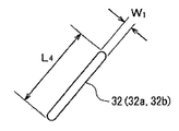
또한, 도 3에 도시하는 바와 같이, 제1 슬롯(32a)의 길이와, 제2 슬롯(32b)의 길이는, 모두 동일하다[슬롯 길이(L4)]. 또한, 제1 슬롯(32a)의 폭과, 제2 슬롯(32b)의 폭은, 모두 동일하다[슬롯 폭(W1)]. 슬롯 길이와 슬롯 폭의 비(L4/W1)는, 방사 효율(전자파 도입의 전력 효율)을 높이는 관점에서, 1 ∼ 26의 범위가 바람직하다. 또한, 슬롯 길이(L4)는, 예컨대 40 ㎜ ∼ 80 ㎜의 범위로 할 수 있다. 또한, 슬롯 폭(W1)은, 예컨대 3 ㎜ ∼ 40 ㎜의 범위로 할 수 있다. In addition, as shown in FIG. 3, the length of the
또한, 지파판(33)의 재질이 석영인 경우의 지파판(33)의 두께와, 평면 안테나판(31)의 제1 슬롯(32a) 및 제2 슬롯(32b)의 직경 방향의 위치[비(L1/r) 및 비(L2/r)]의 관계에 대해서는, 석영의 유전율에 의한 파장 단축과 석영 내에서의 정재파의 주기성을 고려하여, 정재파의 파장으로 설정하는 것이 바람직하다.In addition, the thickness of the slow wave plate 33 when the material of the slow wave plate 33 is quartz, and the position [ratio] of the
다음으로, 본 실시형태에 따른 플라즈마 처리 장치(100)를 이용한 플라즈마 처리의 순서의 일례에 대해서 설명한다. 여기서는, 처리 가스로서 산소를 함유하는 가스를 이용하여, 웨이퍼 표면을 플라즈마 산화 처리하는 경우를 예로 든다.Next, an example of the procedure of the plasma processing using the
먼저, 예컨대 사용자 인터페이스(52)로부터, 플라즈마 처리 장치(100)로 플라즈마 산화 처리를 행하도록, 지령이 입력된다. 이 지령을 받아, 프로세스 컨트롤러(51)는, 기억부(53)에 보존된 레시피를 판독한다. 그리고, 그 레시피에 기초하는 조건으로 플라즈마 산화 처리가 실행되도록, 프로세스 컨트롤러(51)로부터 플라즈마 처리 장치(100)의 각 엔드 디바이스, 예컨대 가스 공급부(18), 배기 장치(24), 전자파 발생 장치(39), 히터 전원(5a) 등에 제어 신호가 송출된다.First, a command is input, for example, from the
그리고, 게이트 밸브(17)가 개방되고, 반입출구(16)로부터 웨이퍼(W)가 챔버(1) 내에 반입되어, 배치대(2) 상에 배치된다. 다음으로, 챔버(1) 내부가 감압 배기되면서, 가스 공급부(18)로부터, 비활성 가스 및 산소 함유 가스가 미리 정해진 유량으로 각각 가스 도입부(15)를 통해 챔버(1) 내에 도입된다. 또한, 배기량 및 가스 공급량이 조정되어, 챔버(1) 내부가 미리 정해진 압력으로 조절된다.Then, the gate valve 17 is opened, the wafer W is loaded into the chamber 1 from the carrying in and out
다음으로, 전자파 발생 장치(39)의 파워를 온(입력)으로 하여, 전자파(800 ㎒ ∼ 1000 ㎒)를 발생시킨다. 그리고, 종래의 마이크로파의 주파수보다도 낮은 주파수, 예컨대 915 ㎒의 전자파가, 매칭 회로(38)를 통해 도파관(37)으로 유도된다. 도파관(37)으로 유도된 전자파는, 직사각형 도파관(37b) 및 동축 도파관(37a)을 순차적으로 통과하여, 내부 도체(41)를 통해 평면 안테나판(31)에 공급된다. 전자파는, 직사각형 도파관(37b) 내에서는 TE 모드로 전파한다. 이 TE 모드의 전자파는, 모드 변환기(40)에서 TEM 모드로 변환되어, 동축 도파관(37a) 내부를 평면 안테나판(31)을 향하여 전파해 간다. 그리고, 그 전자파는, 평면 안테나판(31)에 관통 형성된 구멍인 슬롯(32)으로부터, 투과판(28)을 통해, 챔버(1) 내에서의 웨이퍼(W)의 상방 공간으로 방사된다. 전자파 출력(전력)은, 전자파(전자계)를 효율적으로 공급한다는 관점에서, 평면 안테나판(31)의 면적 1 ㎠당의 파워 밀도로서, 0.41 W/㎠ ∼ 4.19 W/㎠의 범위인 것이 바람직하다. 전자파 출력은, 예컨대 500 W ∼ 5000 W 정도의 범위에서, 목적에 따라, 상기 범위의 파워 밀도가 되도록 선택할 수 있다.Next, the power of the
평면 안테나판(31)으로부터 투과판(28)을 경유하여 챔버(1)로 방사되는 전자파에 의해, 챔버(1) 내에서 균일하게 전자계가 형성되어, 비활성 가스 및 산소 함유 가스가 각각 플라즈마화된다. 전자계에 의해 여기되는 그 플라즈마는, 전자계가 평면 안테나판(31)의 다수의 슬롯(32)으로부터 방사됨으로써, 109/㎤ ∼ 1013/㎤의 고밀도이며, 웨이퍼(W) 근방에서는 대략 1.5 eV 이하의 저전자 온도의 플라즈마가 된다. 이렇게 하여 형성되는 고밀도 플라즈마는, 하지막에의 이온 등에 의한 플라즈마 손상이 적은 것이다. 그리고, 플라즈마 중의 활성종, 예컨대 라디칼이나 이온의 작용에 의해, 웨이퍼(W)의 실리콘 표면이 산화되어 실리콘 산화막 SiO2의 박막이 형성된다. 또한, 산소 함유 가스를 대신하여 질소 가스를 이용함으로써, 실리콘의 질화 처리가 가능하다. 또한, 성막(成膜) 원료 가스를 이용함으로써, 플라즈마 CVD법에 의한 성막을 행할 수도 있다.Electromagnetic waves are uniformly formed in the chamber 1 by the electromagnetic waves radiated from the
프로세스 컨트롤러(51)로부터 플라즈마 처리를 종료시키는 제어 신호가 송출되면, 전자파 발생 장치(39)의 파워가 오프(차단)되어, 플라즈마 산화 처리가 종료된다. 다음으로, 가스 공급부(18)로부터의 처리 가스의 공급이 정지되고, 챔버 내부가 탈기된다. 그리고, 웨이퍼(W)가 챔버(1) 내부로부터 반출되어, 1장의 웨이퍼(W)에 대한 플라즈마 처리가 종료된다.When the control signal for terminating the plasma process is sent from the
플라즈마 처리 장치(100)에서는, 본원 발명에 따른 평면 안테나판(31)의 슬롯 패턴을, 전자파 발생 장치(39)에서 발생되는 전자파의 주파수를 종래의 마이크로파의 주파수보다 낮은 800 ㎒ ∼ 1000 ㎒의 범위(바람직하게는 915 ㎒)로 적용 가능하게 설정하고 있다. 이와 같이, 플라즈마 생성용 전자파로서 주파수가 800 ㎒ ∼ 1000 ㎒의 범위인 것을 사용함으로써, 예컨대 종래의 2.45 ㎓의 주파수의 마이크로파를 사용하는 경우와 비교하여, 표면파 플라즈마가 컷오프되는 플라즈마 밀도(컷오프 밀도)가 저하되어, 보다 높은 압력 조건까지 높은 전력 효율로 안정적으로 플라즈마를 균일하게 생성할 수 있다.In the
도 5는 플라즈마 처리 장치(100)에서 행해지는 플라즈마 처리의 처리 압력과 플라즈마의 전자 밀도의 관계를 도시하고 있다. 처리 압력이 높아짐에 따라, 플라즈마의 전자 밀도는 저하되고, 컷오프 밀도에 있어서 전자 밀도는 급격하게 감소한다. 여기서, 2.45 ㎓의 마이크로파 플라즈마의 컷오프 밀도는, 약 7.5×1010 cm-3이지만, 915 ㎒의 전자파 플라즈마의 컷오프 밀도는, 약 1.0×1010 cm-3이다. 또한, 도 5에 도시한 바와 같이, 2.45 ㎓의 마이크로파 플라즈마에 비하여, 915 ㎒의 전자파 플라즈마에서는, 보다 높은 압력 조건까지 컷오프 밀도 이상의 플라즈마 밀도를 유지할 수 있다.FIG. 5 shows the relationship between the processing pressure of the plasma processing performed in the
또한, 본 실시형태의 평면 안테나판(31)에서는, 평면 안테나판(31)의 중심(OA)으로부터 내측의 제1 슬롯(32a)의 중심(O32a)까지의 거리(L1)와 평면 안테나판(31)의 반경(r)의 비(L1/r)를 0.35 ∼ 0.5의 범위로 하고, 평면 안테나판(31)의 중심(OA)으로부터 외측의 제2 슬롯(32b)의 중심(O32b)까지의 거리(L2)와 평면 안테나판(31)의 반경(r)의 비(L2/r)를 0.7 ∼ 0.85의 범위로 했기 때문에, 전자파 발생 장치(39)에서 발생되는 전자파의 주파수를 800 ㎒ ∼ 1000 ㎒라고 하는 범위로 해도, 반사파의 발생을 억제할 수 있고, 챔버(1) 내에 효율적으로 전자파를 도입할 수 있다. 따라서, 챔버 내에서 표면파 플라즈마를 균일하게 안정적으로 유지할 수 있다.In the
또한, 본 실시형태의 평면 안테나판(31)에서는, 평면 안테나판(31)의 중심(OA)과 제1 슬롯(32a)의 중심(O32a)을 연결하는 직선에 대하여, 그 제1 슬롯(32a)의 길이 방향이 이루는 각도(θ1)를 30°∼ 50°의 범위로 하고, 평면 안테나판(31)의 중심(OA)과 제2 슬롯(32b)의 중심(O32b)을 연결하는 직선에 대하여, 그 제2 슬롯(32b)의 길이 방향이 이루는 각도(θ2)를 130°∼ 150°의 범위로 하고 있으며, 또한, 평면 안테나판(31)의 중심(OA)으로부터 제1 슬롯(32a)의 중심(O32a)까지를 연결하는 직선과 평면 안테나판(31)의 중심(OA)으로부터 제2 슬롯(32b)의 중심(O32b)까지를 연결하는 직선이 이루는 각도(θ3)를 8°∼ 15°의 범위로 하고, 제1 슬롯(32a)의 길이 방향과 제2 슬롯(32b)의 길이 방향이 이루는 각도(θ4)를 대략 직각 예컨대 85°∼ 95°의 범위로 하고 있다. 이들 각도(θ1, θ2, θ3 및 θ4)가, 상기 범위로 규정됨으로써, 슬롯(32)을 통해 전자파를 높은 전력 효율로 챔버(1) 내에 도입함으로써 적합하게 플라즈마를 생성할 수 있다.In the
이상과 같이, 본 실시형태의 평면 안테나판(31)에 따르면, 슬롯(32a, 32b)의 배치를 상술한 바와 같이 고안함으로써, 종래의 마이크로파의 주파수보다도 낮은 800 ㎒ ∼ 1000 ㎒의 범위(바람직하게는 915 ㎒)의 주파수의 전자파를 챔버(1) 내에 효율적으로 도입할 수 있다. 따라서, 종래의 2.45 ㎓의 마이크로파를 사용하는 경우와 비교하여, 보다 높은 압력 조건이라도, 플라즈마 처리 장치(100)의 챔버(1) 내에서 표면파 플라즈마를 균일하게 안정적으로 유지할 수 있다. 그리고, 이러한 플라즈마 처리 장치(100)를 이용함으로써, 비교적 높은 압력 조건에서, 처리율의 향상이나 웨이퍼면 내에서의 처리의 균일성을 실현할 수 있어, 높은 정밀도가 필요한 3차원 디바이스 가공이나 미세 가공 및 대구경에 대한 대응을 도모할 수 있다.As described above, according to the
[제2 실시형태]Second Embodiment
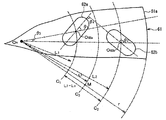
다음으로, 도 6 및 도 7을 참조하면서, 본 발명의 제2 실시형태에 따른 평면 안테나판(61)에 대해서 설명한다. 도 6은 제2 실시형태에 따른 평면 안테나판(61)의 주요부를 도시하는 평면도이고, 도 7은 평면 안테나판(61)에서의 슬롯을 확대하여 도시하는 평면도이다. 본 실시형태에 따른 평면 안테나판(61)은, 제1 실시형태에 따른 평면 안테나판(31)과 마찬가지로, 플라즈마 처리 장치(100)에 사용되는 것이다.Next, the
평면 안테나판(61)은, 원판형의 기재(61a)와, 이 기재(61a)에 미리 정해진 패턴으로 관통 형성된 쌍을 이루는 다수의 슬롯[62(62a, 62b)]을 갖고 있다. 평면 안테나판(61)에서는, 각 슬롯(62)의 폭(W2)이 크게 형성되어, 슬롯(62)의 배치수가 적어지고 있는 점을 제외하면, 제1 실시형태의 평면 안테나판(31)과 동일한 구성을 갖고 있다. 따라서, 이하의 설명에서는, 제1 실시형태와의 차이점을 중심으로 설명하고, 동일한 구성에는 동일한 부호를 붙이고 설명을 생략한다.The
기재(61a)에 형성된 개개의 슬롯(62)은, 약간 폭이 넓고 가늘고 긴 형상이다. 슬롯(62)은, 평면 안테나판(61)의 중심(OA)에 가까운 위치에 둘레 방향으로 배열된 복수의 제1 슬롯(62a)과, 이들 제1 슬롯(62a)을 둘러싸도록 외측에 배열된 복수의 제2 슬롯(62b)을 포함한다. 제1 슬롯(62a)과 제2 슬롯(62b)은, 동심원 형상으로 배열된다.Each
제1 슬롯(62a)과 제2 슬롯(62b)은 쌍을 이루고 있고, 각 8개씩이 평면 안테나판(61)의 동심원 형상으로 균등하게 배치된다. 여기서, 평면 안테나판(61)의 중심(OA)[기재(61a)의 중심과 동일]으로부터 제1 슬롯(62a)의 중심(O62a)까지의 거리(L1)와 평면 안테나판(61)의 반경(r)의 비(L1/r)는, 0.35 ∼ 0.5 범위이다. 또한, 평면 안테나판(61)의 중심(OA)으로부터 제2 슬롯(62b)의 중심(O62b)까지의 거리(L2)와 평면 안테나판(61)의 반경(r)의 비(L2/r)는, 0.7 ∼ 0.85의 범위이다. 비(L1/r) 및 비(L2/r)를 상기 범위로 규정한 이유에 대해서는, 제1 실시형태와 동일하다.The
또한, 평면 안테나판(61)과 동심이며 반경이 거리(L1)이고 제1 슬롯(62a)의 중심(O62a)을 지나는 원을 C1로 하고, 평면 안테나판(61)과 동심이며 반경이 거리(L2)이고 제2 슬롯(62b)의 중심(O62b)을 지나는 원을 C2로 한 경우에, 평면 안테나판(61)과 동심이며 평면 안테나판(61)의 중심(OA)으로부터 원(C1)과 원(C2)의 원주의 직경 방향의 중간점(M)까지의 거리(L3)를 반경으로 한 원(C3)에 대해서, 그 거리(L3)와 평면 안테나판(61)의 반경(r)의 비(L3/r)가, 0.5 ∼ 0.7의 범위인 것이 바람직하다. 그 비(L3/r)를 0.5 ∼ 0.7의 범위로 규정함으로써, 반사파의 발생이 억제되고, 전자파가 효율적으로 슬롯으로부터 도입되어, 챔버(1) 내에 균일하게 안정된 플라즈마를 형성할 수 있다.In addition, a circle concentric with the
또한, 거리(L2) 및 거리(L1)의 차분(L2-L1)과 평면 안테나판(61)의 반경(r)의 비[(L2-L1)/r]는, 0.2 ∼ 0.5의 범위인 것이 바람직하다. 그 비[(L2-L1)/r]를 상기 범위로 규정함으로써, 반사파의 발생이 억제되고, 전자파가 효율적으로 슬롯으로부터 도입되어, 챔버(1) 내에 균일하게 안정된 플라즈마를 형성할 수 있다.In addition, the ratio [(L2-L1) / r] of the difference L2-L1 between the distance L2 and the distance L1 and the radius r of the
또한, 도 6에 도시한 각도(θ1, θ2, θ3 및 θ4)의 범위(및 그 범위로 설정된 이유)는, 모두, 제1 실시형태와 동일하다.In addition, the range (and the reason set to the range) of angle (theta) 1, (theta) 2, (theta) 3, and (theta) 4 shown in FIG. 6 is the same as that of 1st Embodiment.
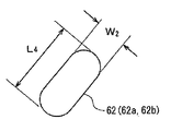
본 실시형태의 평면 안테나판(61)에서는, 도 7에 도시한 바와 같이, 제1 슬롯(62a)의 길이와, 제2 슬롯(62b)의 길이는, 모두 동일하다[슬롯 길이(L4)]. 또한, 제1 슬롯(62a)의 폭과, 제2 슬롯(62b)의 폭도, 모두 동일하다[슬롯 폭(W2)]. 슬롯 길이와 슬롯 폭의 비(L4/W2)는, 평면 안테나판(61)에 있어서 각 슬롯으로부터의 전자파의 방사 효율(전력 효율)을 높이는 관점에서, 1 ∼ 26의 범위로 하는 것이 바람직하다. 또한, 슬롯 길이(L4)는, 예컨대 40 ㎜ ∼ 80 ㎜의 범위, 슬롯 폭(W2)은, 예컨대 3 ㎜ ∼ 40 ㎜의 범위로 할 수 있으나, 본 실시형태에서는, 제1 실시형태의 평면 안테나판(31)과 비교하여, 슬롯 폭(W2)의 비율이 커지도록 설정하였다. 이에 따라, 슬롯(62)에 의한 관통구의 면적이 커져, 평면 안테나판(61)의 슬롯(62)을 통해 전자파를 효율적으로 챔버(1) 내에 도입시킬 수 있다.In the
본 실시형태에서의 그 외의 구성, 작용 및 효과는, 제1 실시형태와 동일하다.The other structure, effect | action, and effect in this embodiment are the same as that of 1st embodiment.
[제3 실시형태][Third Embodiment]
다음으로, 도 8을 참조하면서, 본 발명의 제3 실시형태에 따른 평면 안테나판(71)에 대해서 설명한다. 도 8은 제3 실시형태에 따른 평면 안테나판(71)의 주요부를 도시하는 평면도이다. 본 실시형태에 따른 평면 안테나판(71)은, 제1 실시형태에 따른 평면 안테나판(31)과 마찬가지로, 플라즈마 처리 장치(100)에 사용되는 것이다. 평면 안테나판(71)은, 외주측에 배치된 슬롯의 수가 많이 형성된 점을 제외하고, 제2 실시형태의 평면 안테나판(61)과 동일한 구성을 갖는다. 따라서, 이하의 설명에서는, 제2 실시형태와의 차이점을 중심으로 설명하고, 동일한 구성에는 동일한 부호를 붙이고 설명을 생략한다.Next, the
평면 안테나판(71)은, 원판형의 기재(71a)와, 이 기재(71a)에 미리 정해진 패턴으로 관통 형성된 다수의 슬롯[72(72a, 72b1, 72b2)]을 갖는다. 슬롯(72)은, 평면 안테나판(71)의 중심(OA)에 가까운 위치에 둘레 방향으로 배열된 복수의 제1 슬롯(72a)과, 이들 제1 슬롯(72a)을 둘러싸도록 외측에 배열된 복수의 제2 슬롯(72b1) 및 제3 슬롯(72b2)을 포함한다.The
제1 슬롯(72a)과 제2 슬롯(72b1) 및 제3 슬롯(72b2)은, 동심원 형상으로 배열된다. 또한, 제1 슬롯(72a)과 제2 슬롯(72b1)은, 쌍을 이루고 있다. 한편, 제3 슬롯(72b2)은, 제1 슬롯(72a)과는 쌍을 이루고 있지 않은 비쌍(不對) 슬롯이다. 제1 슬롯(72a)은, 평면 안테나판(71)의 원주 방향으로 8개 균등하게 배치된다. 외주측의 슬롯 중 제1 슬롯(72a)과 쌍을 이루는 제2 슬롯(72b1)도, 평면 안테나판(71)의 원주 방향으로 8개 균등하게 배치된다.The
한편, 제2 슬롯(72b1) 및 제3 슬롯(72b2)은, 각 8개씩(합계 16개)가, 평면 안테나판(71)의 원주 방향으로 균등하게 배치된다. 제2 슬롯(72b1)과 제3 슬롯(72b2)은, 1개 간격으로 교대로 배치되어 있다. 평면 안테나판(71)에서는, 제2 슬롯(72b1)에 더하여 제3 슬롯(72b2)을 배치함으로써, 평면 안테나판(71)에서의 관통구의 면적이, 제2 실시형태의 평면 안테나판(61)보다도, 더 증대되어 있다. 따라서, 전자파를 더 효율적으로 챔버(1) 내에 도입시킬 수 있다.On the other hand, eight (16 total) of 2nd slot 72b1 and 3rd slot 72b2 is arrange | positioned equally in the circumferential direction of the
본 실시형태의 평면 안테나판(71)에서도, 평면 안테나판(71)의 중심(OA)[기재(71a)의 중심과 동일]으로부터 제1 슬롯(72a)의 중심(O72a)까지의 거리(L1)와 평면 안테나판(71)의 반경(r)의 비(L1/r)는, 0.35 ∼ 0.5의 범위이다. 또한, 평면 안테나판(71)의 중심(OA)으로부터 제2 슬롯(72b1), 제3 슬롯(72b2)의 중심(O72b1, O72b2)까지의 거리(L2)와 평면 안테나판(71)의 반경(r)의 비(L2/r)는, 0.7 ∼ 0.85의 범위이다. 비(L1/r) 및 비(L2/r)를 상기 범위로 규정한 이유에 대해서는, 제1 실시형태와 동일하다. 상기 범위로 규정함으로써, 반사파의 발생이 억제되고, 전자파가 효율적으로 챔버(1) 내에 공급되어 안정된 플라즈마를 형성할 수 있다.Distance to the center (O 72a) of the first slot (72a) from [the center the same as a base material (71a)] center (O A) of in the
또한, 평면 안테나판(71)과 동심이며 반경이 거리(L1)이고 제1 슬롯(72a)의 중심(O72a)을 지나는 원을 C1로 하고, 평면 안테나판(71)과 동심이며 반경이 거리(L2)이고 제2 슬롯(72b1)의 중심(O72b1)을 지나는 원을 C2로 한 경우에, 평면 안테나판(71)과 동심이며 평면 안테나판(71)의 중심(OA)으로부터 원(C1)과 원(C2)의 원주의 직경 방향의 중간점(M)까지의 거리(L3)를 반경으로 한 원(C3)에 대해서, 그 거리(L3)와 평면 안테나판(71)의 반경(r)의 비(L3/r)가, 0.5 ∼ 0.7의 범위인 것이 바람직하다. 그 비(L3/r)를 0.5 ∼ 0.7의 범위로 규정함으로써, 반사파의 발생이 억제되고, 전자파가 효율적으로 챔버(1) 내에 공급되어 안정된 플라즈마를 형성할 수 있다.In addition, a circle concentric with the
또한, 거리(L2) 및 거리(L1)의 차분(L2-L1)과 평면 안테나판(71)의 반경(r)의 비[(L2-L1)/r]는, 0.2 ∼ 0.5의 범위인 것이 바람직하다. 그 비[(L2-L1)/r]를 상기 범위로 규정함으로써, 반사파의 발생이 억제되고, 전자파가 효율적으로 챔버(1) 내에 공급되어 안정된 플라즈마를 형성할 수 있다.In addition, the ratio [(L2-L1) / r] of the difference L2-L1 of the distance L2 and the distance L1 and the radius r of the
또한, 도 8에 도시한 각도(θ1, θ2, θ3 및 θ4)의 범위(및 그 범위로 설정된 이유)는, 모두, 제1 실시형태와 동일하다.In addition, the range (and the reason set to the range) of angle (theta) 1, (theta) 2, (theta) 3, and (theta) 4 shown in FIG. 8 is the same as that of 1st Embodiment.
또한, 본 실시형태에서의 제1 슬롯(72a), 제2 슬롯(72b1), 및 제3 슬롯(72b2)의 길이 및 폭의 범위, 및 그 범위로 규정되는 이유는, 모두 제2 실시형태와 동일하다.In addition, the range of the length and width of the
본 실시형태에서의 그 외의 구성, 작용 및 효과는, 제1 실시형태와 동일하다.The other structure, effect | action, and effect in this embodiment are the same as that of 1st embodiment.
이상, 본 발명의 실시형태에 대해서 기술하였으나, 본 발명은 상기 실시형태에 제약되는 것은 아니며, 여러 가지 변형이 가능하다. 예컨대, 본 발명에 따른 슬롯 패턴을 갖는 평면 안테나판(31)을 구비한 플라즈마 처리 장치(100)는, 플라즈마 산화 처리 장치, 플라즈마 질화 처리 장치, 플라즈마 CVD 처리 장치, 플라즈마 에칭 처리 장치, 플라즈마 애싱 처리 장치 등에 적용할 수 있다. 또한, 본 발명에 따른 평면 안테나판을 구비한 플라즈마 처리 장치는, 피처리체로서 반도체 웨이퍼를 처리하는 경우에 한정되지 않고, 예컨대 액정 디스플레이 장치나 유기 EL 디스플레이 장치 등의 평판 디스플레이 장치용 기판을 피처리체로 하는 플라즈마 처리 장치에도 적용할 수 있다.As mentioned above, although embodiment of this invention was described, this invention is not restrict | limited to the said embodiment, A various deformation | transformation is possible. For example, the
또한, 각 슬롯의 평면 형상에 대해서도, 상기 실시형태에서 나타낸 형상에 한정되는 것은 아니며, 예컨대 원형, 타원형, 정사각형, 직사각형 등의 형상을 채용할 수 있다.In addition, also about the planar shape of each slot, it is not limited to the shape shown by the said embodiment, For example, shapes, such as a circle, an ellipse, square, a rectangle, can be employ | adopted.
Claims (15)
도전성 재료로 이루어지는 평판형 기재와,
상기 평판형 기재에 형성된, 전자파를 방사하는 복수의 관통구를 구비하고,
상기 관통구는, 상기 평면 안테나 부재의 중심에 그 중심이 겹쳐지는 원의 둘레 상에 배열된 복수의 제1 관통구와, 상기 제1 관통구의 외측에 상기 원과 동심원 형상으로 배열된 복수의 제2 관통구를 포함하며,
상기 평면 안테나 부재의 중심으로부터 상기 제1 관통구의 중심까지의 거리(L1)와, 상기 평면 안테나 부재의 반경(r)의 비(L1/r)는, 0.35 ∼ 0.5의 범위이고,
상기 평면 안테나 부재의 중심으로부터 상기 제2 관통구의 중심까지의 거리(L2)와, 상기 평면 안테나 부재의 반경(r)의 비(L2/r)는, 0.7 ∼ 0.85의 범위인 것을 특징으로 하는 평면 안테나 부재.A flat antenna member for introducing electromagnetic waves generated from an electromagnetic wave source into a processing vessel of a plasma processing apparatus,
A flat substrate made of a conductive material,
And a plurality of through holes formed in the flat substrate to emit electromagnetic waves,
The through holes may include a plurality of first through holes arranged on a circumference of a circle whose center overlaps a center of the planar antenna member, and a plurality of second through holes arranged concentrically with the circle on the outside of the first through hole. Contains a sphere,
The distance L1 from the center of the planar antenna member to the center of the first through hole and the ratio L1 / r of the radius r of the planar antenna member are in the range of 0.35 to 0.5,
The distance L2 from the center of the planar antenna member to the center of the second through hole and the ratio L2 / r of the radius r of the planar antenna member are in the range of 0.7 to 0.85. Antenna member
상기 제1 관통구의 길이 방향에 대하여, 상기 제2 관통구의 길이 방향이 이루는 각도는, 85°∼ 95°의 범위인 것을 특징으로 하는 평면 안테나 부재.The said 1st through hole and the said 2nd through hole are both elongate shape, in any one of Claims 1-3,
An angle formed by the longitudinal direction of the second through hole with respect to the longitudinal direction of the first through hole is in the range of 85 ° to 95 °.
상기 처리 용기 내에 가스를 공급하는 가스 도입부와,
상기 처리 용기 내부를 감압 배기하는 배기 장치와,
상기 처리 용기의 상부의 개구부에 기밀하게 장착되고, 상기 처리 용기 내에 플라즈마를 생성하기 위한 전자파를 투과시키는 투과판과,
상기 투과판 위에 배치되고, 상기 전자파를 상기 처리 용기 내에 도입하는 평면 안테나 부재와,
상기 평면 안테나 부재를 상방으로부터 덮는 커버 부재와,
상기 커버 부재를 관통하여 설치되고, 전자파 발생원에서 발생된 800 ㎒ ∼ 1000 ㎒의 범위의 전자파를 상기 평면 안테나 부재에 공급하는 도파관을 구비하며,
상기 평면 안테나 부재는,
도전성 재료로 이루어지는 평판형 기재와,
상기 평판형 기재에 형성된, 전자파를 방사하는 복수의 관통구를 가지며,
상기 관통구는, 원형 형상으로 배열된 복수의 제1 관통구와, 상기 제1 관통구의 외측에 동심원 형상으로 배열된 복수의 제2 관통구를 포함하며,
상기 평면 안테나 부재의 중심으로부터 상기 제1 관통구의 중심까지의 거리(L1)와, 상기 평면 안테나 부재의 반경(r)의 비(L1/r)는, 0.35 ∼ 0.5의 범위이고,
상기 평면 안테나 부재의 중심으로부터 상기 제2 관통구의 중심까지의 거리(L2)와, 상기 평면 안테나 부재의 반경(r)의 비(L2/r)는, 0.7 ∼ 0.85의 범위인 것을 특징으로 하는 플라즈마 처리 장치.A degassable treatment container for receiving a target object;
A gas introduction unit for supplying gas into the processing container;
An exhaust device for evacuating the inside of the processing container under reduced pressure;
A transmissive plate that is hermetically mounted to an opening in the upper portion of the processing container and transmits electromagnetic waves for generating plasma in the processing container;
A planar antenna member disposed on the transmission plate and introducing the electromagnetic wave into the processing container;
A cover member covering the planar antenna member from above;
It is provided through the cover member, and provided with a waveguide for supplying the electromagnetic wave in the range of 800 MHz to 1000 MHz generated from the electromagnetic wave source to the planar antenna member,
The flat antenna member,
A flat substrate made of a conductive material,
And a plurality of through holes formed in the flat substrate to emit electromagnetic waves,
The through hole includes a plurality of first through holes arranged in a circular shape, and a plurality of second through holes arranged in a concentric shape on an outer side of the first through hole,
The distance L1 from the center of the planar antenna member to the center of the first through hole and the ratio L1 / r of the radius r of the planar antenna member are in the range of 0.35 to 0.5,
The distance L2 from the center of the planar antenna member to the center of the second through hole and the ratio L2 / r of the radius r of the planar antenna member are in the range of 0.7 to 0.85. Processing unit.
상기 제1 관통구의 길이 방향에 대하여, 상기 제2 관통구의 길이 방향이 이루는 각도는, 85°∼ 95°의 범위인 것을 특징으로 하는 플라즈마 처리 장치.The said 1st through hole and the said 2nd through hole are both elongate shape, in any one of Claims 9-11,
An angle formed by the longitudinal direction of the second through hole with respect to the longitudinal direction of the first through hole is in the range of 85 ° to 95 °.
15. The method according to any one of claims 9 to 14, wherein a straight line connecting the center of the planar antenna member to the center of the first through hole is connected to the center of the second through hole from the center of the planar antenna member. An angle formed by a straight line is in a range of 8 ° to 15 °.
Applications Claiming Priority (2)
| Application Number | Priority Date | Filing Date | Title |
|---|---|---|---|
| JP2008065635A JP2009224455A (en) | 2008-03-14 | 2008-03-14 | Flat antenna member and plasma processing device with the same |
| JPJP-P-2008-065635 | 2008-03-14 |
Publications (1)
| Publication Number | Publication Date |
|---|---|
| KR20100122894A true KR20100122894A (en) | 2010-11-23 |
Family
ID=41065337
Family Applications (1)
| Application Number | Title | Priority Date | Filing Date |
|---|---|---|---|
| KR1020107007491A KR20100122894A (en) | 2008-03-14 | 2009-03-13 | Flat antenna member and a plasma processing device provided with same |
Country Status (5)
| Country | Link |
|---|---|
| US (1) | US20110114021A1 (en) |
| JP (1) | JP2009224455A (en) |
| KR (1) | KR20100122894A (en) |
| CN (1) | CN101849444B (en) |
| WO (1) | WO2009113680A1 (en) |
Cited By (1)
| Publication number | Priority date | Publication date | Assignee | Title |
|---|---|---|---|---|
| US10755899B2 (en) | 2014-06-30 | 2020-08-25 | Semes Co., Ltd. | Substrate treating apparatus |
Families Citing this family (3)
| Publication number | Priority date | Publication date | Assignee | Title |
|---|---|---|---|---|
| US8884526B2 (en) | 2012-01-20 | 2014-11-11 | Taiwan Semiconductor Manufacturing Co., Ltd. | Coherent multiple side electromagnets |
| CN103647128B (en) * | 2013-12-23 | 2016-05-11 | 西南交通大学 | A kind of high power RADIAL hermetyic window |
| CN110724938B (en) | 2014-05-16 | 2022-02-22 | 应用材料公司 | Spray head design |
Family Cites Families (16)
| Publication number | Priority date | Publication date | Assignee | Title |
|---|---|---|---|---|
| JPH03191073A (en) * | 1989-12-21 | 1991-08-21 | Canon Inc | Microwave plasma treating device |
| JP3136054B2 (en) * | 1994-08-16 | 2001-02-19 | 東京エレクトロン株式会社 | Plasma processing equipment |
| JPH11251299A (en) * | 1998-03-03 | 1999-09-17 | Hitachi Ltd | Method and apparatus for plasma treating |
| JPH11260594A (en) * | 1998-03-12 | 1999-09-24 | Hitachi Ltd | Plasma processing device |
| JP3430053B2 (en) * | 1999-02-01 | 2003-07-28 | 東京エレクトロン株式会社 | Plasma processing equipment |
| JP4478352B2 (en) * | 2000-03-29 | 2010-06-09 | キヤノン株式会社 | Plasma processing apparatus, plasma processing method, and structure manufacturing method |
| JP4504511B2 (en) * | 2000-05-26 | 2010-07-14 | 忠弘 大見 | Plasma processing equipment |
| JP4598247B2 (en) * | 2000-08-04 | 2010-12-15 | 東京エレクトロン株式会社 | Radial antenna and plasma apparatus using the same |
| JP4183934B2 (en) * | 2001-10-19 | 2008-11-19 | 尚久 後藤 | Microwave plasma processing apparatus, microwave plasma processing method, and microwave power supply apparatus |
| JP3914071B2 (en) * | 2002-03-12 | 2007-05-16 | 東京エレクトロン株式会社 | Plasma processing equipment |
| JP2004235434A (en) * | 2003-01-30 | 2004-08-19 | Rohm Co Ltd | Plasma processing system |
| US6998565B2 (en) * | 2003-01-30 | 2006-02-14 | Rohm Co., Ltd. | Plasma processing apparatus |
| JP4149427B2 (en) * | 2004-10-07 | 2008-09-10 | 東京エレクトロン株式会社 | Microwave plasma processing equipment |
| JP2006244891A (en) * | 2005-03-04 | 2006-09-14 | Tokyo Electron Ltd | Microwave plasma processing device |
| US20080190560A1 (en) * | 2005-03-04 | 2008-08-14 | Caizhong Tian | Microwave Plasma Processing Apparatus |
| JP4997826B2 (en) * | 2006-05-22 | 2012-08-08 | 東京エレクトロン株式会社 | Planar antenna member and plasma processing apparatus using the same |
-
2008
- 2008-03-14 JP JP2008065635A patent/JP2009224455A/en active Pending
-
2009
- 2009-03-13 CN CN2009801009072A patent/CN101849444B/en not_active Expired - Fee Related
- 2009-03-13 US US12/922,402 patent/US20110114021A1/en not_active Abandoned
- 2009-03-13 WO PCT/JP2009/054922 patent/WO2009113680A1/en active Application Filing
- 2009-03-13 KR KR1020107007491A patent/KR20100122894A/en not_active Application Discontinuation
Cited By (1)
| Publication number | Priority date | Publication date | Assignee | Title |
|---|---|---|---|---|
| US10755899B2 (en) | 2014-06-30 | 2020-08-25 | Semes Co., Ltd. | Substrate treating apparatus |
Also Published As
| Publication number | Publication date |
|---|---|
| CN101849444A (en) | 2010-09-29 |
| CN101849444B (en) | 2012-08-29 |
| JP2009224455A (en) | 2009-10-01 |
| WO2009113680A1 (en) | 2009-09-17 |
| US20110114021A1 (en) | 2011-05-19 |
Similar Documents
| Publication | Publication Date | Title |
|---|---|---|
| TWI549156B (en) | A plasma processing device and a microwave introduction device | |
| KR101196075B1 (en) | Plasma processing device | |
| KR101176061B1 (en) | Top plate and plasma processing apparatus | |
| KR101208884B1 (en) | Microwave introduction mechanism, microwave plasma source and microwave plasma processing device | |
| KR100960424B1 (en) | Microwave plasma processing device | |
| US20080134974A1 (en) | Plasma processing apparatus and gas through plate | |
| JP5096047B2 (en) | Microwave plasma processing apparatus and microwave transmission plate | |
| KR20130018823A (en) | Plasma nitridization method | |
| JP2010232493A (en) | Plasma processing device | |
| JP5422396B2 (en) | Microwave plasma processing equipment | |
| KR20100122894A (en) | Flat antenna member and a plasma processing device provided with same | |
| JP5479013B2 (en) | Plasma processing apparatus and slow wave plate used therefor | |
| WO2011013633A1 (en) | Planar antenna member and plasma processing device equipped with same | |
| KR101882608B1 (en) | Plasma processing apparatus and plasma processing method | |
| JP5728565B2 (en) | Plasma processing apparatus and slow wave plate used therefor | |
| JP2013033979A (en) | Microwave plasma processing apparatus | |
| JP5066502B2 (en) | Plasma processing equipment | |
| JP2009099975A (en) | Plasma processing device |
Legal Events
| Date | Code | Title | Description |
|---|---|---|---|
| A201 | Request for examination | ||
| E601 | Decision to refuse application |