KR20100102635A - Under bump routing layer method and apparatus - Google Patents
Under bump routing layer method and apparatus Download PDFInfo
- Publication number
- KR20100102635A KR20100102635A KR1020107014910A KR20107014910A KR20100102635A KR 20100102635 A KR20100102635 A KR 20100102635A KR 1020107014910 A KR1020107014910 A KR 1020107014910A KR 20107014910 A KR20107014910 A KR 20107014910A KR 20100102635 A KR20100102635 A KR 20100102635A
- Authority
- KR
- South Korea
- Prior art keywords
- conductor
- solder
- site
- redistribution layer
- layer
- Prior art date
Links
- 238000000034 method Methods 0.000 title claims abstract description 70
- 239000004020 conductor Substances 0.000 claims abstract description 139
- 229910000679 solder Inorganic materials 0.000 claims abstract description 133
- 239000004065 semiconductor Substances 0.000 claims abstract description 121
- 238000004519 manufacturing process Methods 0.000 claims abstract description 17
- 239000000758 substrate Substances 0.000 claims description 41
- 230000008878 coupling Effects 0.000 claims 2
- 238000010168 coupling process Methods 0.000 claims 2
- 238000005859 coupling reaction Methods 0.000 claims 2
- 238000001465 metallisation Methods 0.000 description 59
- 229910052751 metal Inorganic materials 0.000 description 35
- 239000002184 metal Substances 0.000 description 35
- 238000002161 passivation Methods 0.000 description 30
- 230000008569 process Effects 0.000 description 30
- 239000004642 Polyimide Substances 0.000 description 27
- 229920001721 polyimide Polymers 0.000 description 27
- 239000000463 material Substances 0.000 description 22
- 230000008901 benefit Effects 0.000 description 9
- 239000011810 insulating material Substances 0.000 description 8
- 238000007747 plating Methods 0.000 description 7
- 230000035882 stress Effects 0.000 description 7
- VYPSYNLAJGMNEJ-UHFFFAOYSA-N Silicium dioxide Chemical compound O=[Si]=O VYPSYNLAJGMNEJ-UHFFFAOYSA-N 0.000 description 6
- 238000013461 design Methods 0.000 description 6
- RYGMFSIKBFXOCR-UHFFFAOYSA-N Copper Chemical compound [Cu] RYGMFSIKBFXOCR-UHFFFAOYSA-N 0.000 description 5
- RTAQQCXQSZGOHL-UHFFFAOYSA-N Titanium Chemical compound [Ti] RTAQQCXQSZGOHL-UHFFFAOYSA-N 0.000 description 5
- 229910052802 copper Inorganic materials 0.000 description 5
- 239000010949 copper Substances 0.000 description 5
- 229910052719 titanium Inorganic materials 0.000 description 5
- 239000010936 titanium Substances 0.000 description 5
- PXHVJJICTQNCMI-UHFFFAOYSA-N Nickel Chemical compound [Ni] PXHVJJICTQNCMI-UHFFFAOYSA-N 0.000 description 4
- XUIMIQQOPSSXEZ-UHFFFAOYSA-N Silicon Chemical compound [Si] XUIMIQQOPSSXEZ-UHFFFAOYSA-N 0.000 description 4
- 230000015572 biosynthetic process Effects 0.000 description 4
- 238000010586 diagram Methods 0.000 description 4
- 238000005240 physical vapour deposition Methods 0.000 description 4
- 229910052710 silicon Inorganic materials 0.000 description 4
- 239000010703 silicon Substances 0.000 description 4
- 229910052581 Si3N4 Inorganic materials 0.000 description 3
- 238000005229 chemical vapour deposition Methods 0.000 description 3
- 230000000694 effects Effects 0.000 description 3
- 239000003822 epoxy resin Substances 0.000 description 3
- 238000005530 etching Methods 0.000 description 3
- 239000007769 metal material Substances 0.000 description 3
- 239000000203 mixture Substances 0.000 description 3
- 230000002093 peripheral effect Effects 0.000 description 3
- 239000005011 phenolic resin Substances 0.000 description 3
- 229920000647 polyepoxide Polymers 0.000 description 3
- HQVNEWCFYHHQES-UHFFFAOYSA-N silicon nitride Chemical compound N12[Si]34N5[Si]62N3[Si]51N64 HQVNEWCFYHHQES-UHFFFAOYSA-N 0.000 description 3
- BQCADISMDOOEFD-UHFFFAOYSA-N Silver Chemical compound [Ag] BQCADISMDOOEFD-UHFFFAOYSA-N 0.000 description 2
- 229910045601 alloy Inorganic materials 0.000 description 2
- 239000000956 alloy Substances 0.000 description 2
- 229910052782 aluminium Inorganic materials 0.000 description 2
- XAGFODPZIPBFFR-UHFFFAOYSA-N aluminium Chemical compound [Al] XAGFODPZIPBFFR-UHFFFAOYSA-N 0.000 description 2
- 238000003491 array Methods 0.000 description 2
- KUNSUQLRTQLHQQ-UHFFFAOYSA-N copper tin Chemical compound [Cu].[Sn] KUNSUQLRTQLHQQ-UHFFFAOYSA-N 0.000 description 2
- 238000000151 deposition Methods 0.000 description 2
- 238000005137 deposition process Methods 0.000 description 2
- 230000005669 field effect Effects 0.000 description 2
- 239000005350 fused silica glass Substances 0.000 description 2
- 238000001459 lithography Methods 0.000 description 2
- 150000002736 metal compounds Chemical class 0.000 description 2
- 150000002739 metals Chemical class 0.000 description 2
- 238000012986 modification Methods 0.000 description 2
- 230000004048 modification Effects 0.000 description 2
- 229910052759 nickel Inorganic materials 0.000 description 2
- 238000012552 review Methods 0.000 description 2
- 239000000377 silicon dioxide Substances 0.000 description 2
- 229910052709 silver Inorganic materials 0.000 description 2
- 239000004332 silver Substances 0.000 description 2
- 229920003051 synthetic elastomer Polymers 0.000 description 2
- 239000005061 synthetic rubber Substances 0.000 description 2
- 230000008646 thermal stress Effects 0.000 description 2
- 238000012546 transfer Methods 0.000 description 2
- QCEUXSAXTBNJGO-UHFFFAOYSA-N [Ag].[Sn] Chemical compound [Ag].[Sn] QCEUXSAXTBNJGO-UHFFFAOYSA-N 0.000 description 1
- 238000004380 ashing Methods 0.000 description 1
- UMIVXZPTRXBADB-UHFFFAOYSA-N benzocyclobutene Chemical compound C1=CC=C2CCC2=C1 UMIVXZPTRXBADB-UHFFFAOYSA-N 0.000 description 1
- 239000003990 capacitor Substances 0.000 description 1
- 238000003486 chemical etching Methods 0.000 description 1
- 239000011248 coating agent Substances 0.000 description 1
- 238000000576 coating method Methods 0.000 description 1
- 238000004891 communication Methods 0.000 description 1
- 238000007796 conventional method Methods 0.000 description 1
- 238000005336 cracking Methods 0.000 description 1
- 238000012864 cross contamination Methods 0.000 description 1
- 230000005574 cross-species transmission Effects 0.000 description 1
- 230000008021 deposition Effects 0.000 description 1
- 238000009792 diffusion process Methods 0.000 description 1
- 238000010292 electrical insulation Methods 0.000 description 1
- 239000000945 filler Substances 0.000 description 1
- -1 for example Substances 0.000 description 1
- PCHJSUWPFVWCPO-UHFFFAOYSA-N gold Chemical compound [Au] PCHJSUWPFVWCPO-UHFFFAOYSA-N 0.000 description 1
- 239000010931 gold Substances 0.000 description 1
- 229910052737 gold Inorganic materials 0.000 description 1
- 239000012774 insulation material Substances 0.000 description 1
- LQBJWKCYZGMFEV-UHFFFAOYSA-N lead tin Chemical compound [Sn].[Pb] LQBJWKCYZGMFEV-UHFFFAOYSA-N 0.000 description 1
- 230000007246 mechanism Effects 0.000 description 1
- HBVFXTAPOLSOPB-UHFFFAOYSA-N nickel vanadium Chemical compound [V].[Ni] HBVFXTAPOLSOPB-UHFFFAOYSA-N 0.000 description 1
- 230000003287 optical effect Effects 0.000 description 1
- 230000037361 pathway Effects 0.000 description 1
- 229920000642 polymer Polymers 0.000 description 1
- 238000012545 processing Methods 0.000 description 1
- 230000009467 reduction Effects 0.000 description 1
- 239000003870 refractory metal Substances 0.000 description 1
- 239000005368 silicate glass Substances 0.000 description 1
- 235000012239 silicon dioxide Nutrition 0.000 description 1
- 238000005476 soldering Methods 0.000 description 1
- 239000002904 solvent Substances 0.000 description 1
- 235000013599 spices Nutrition 0.000 description 1
- 238000004528 spin coating Methods 0.000 description 1
- 238000003860 storage Methods 0.000 description 1
- 238000001039 wet etching Methods 0.000 description 1
Images


Classifications
-
- H—ELECTRICITY
- H01—ELECTRIC ELEMENTS
- H01L—SEMICONDUCTOR DEVICES NOT COVERED BY CLASS H10
- H01L24/00—Arrangements for connecting or disconnecting semiconductor or solid-state bodies; Methods or apparatus related thereto
- H01L24/01—Means for bonding being attached to, or being formed on, the surface to be connected, e.g. chip-to-package, die-attach, "first-level" interconnects; Manufacturing methods related thereto
- H01L24/10—Bump connectors ; Manufacturing methods related thereto
- H01L24/12—Structure, shape, material or disposition of the bump connectors prior to the connecting process
- H01L24/13—Structure, shape, material or disposition of the bump connectors prior to the connecting process of an individual bump connector
-
- H—ELECTRICITY
- H01—ELECTRIC ELEMENTS
- H01L—SEMICONDUCTOR DEVICES NOT COVERED BY CLASS H10
- H01L21/00—Processes or apparatus adapted for the manufacture or treatment of semiconductor or solid state devices or of parts thereof
- H01L21/02—Manufacture or treatment of semiconductor devices or of parts thereof
- H01L21/04—Manufacture or treatment of semiconductor devices or of parts thereof the devices having potential barriers, e.g. a PN junction, depletion layer or carrier concentration layer
- H01L21/50—Assembly of semiconductor devices using processes or apparatus not provided for in a single one of the subgroups H01L21/06 - H01L21/326, e.g. sealing of a cap to a base of a container
- H01L21/56—Encapsulations, e.g. encapsulation layers, coatings
- H01L21/563—Encapsulation of active face of flip-chip device, e.g. underfilling or underencapsulation of flip-chip, encapsulation preform on chip or mounting substrate
-
- H—ELECTRICITY
- H01—ELECTRIC ELEMENTS
- H01L—SEMICONDUCTOR DEVICES NOT COVERED BY CLASS H10
- H01L23/00—Details of semiconductor or other solid state devices
- H01L23/48—Arrangements for conducting electric current to or from the solid state body in operation, e.g. leads, terminal arrangements ; Selection of materials therefor
- H01L23/50—Arrangements for conducting electric current to or from the solid state body in operation, e.g. leads, terminal arrangements ; Selection of materials therefor for integrated circuit devices, e.g. power bus, number of leads
-
- H—ELECTRICITY
- H01—ELECTRIC ELEMENTS
- H01L—SEMICONDUCTOR DEVICES NOT COVERED BY CLASS H10
- H01L24/00—Arrangements for connecting or disconnecting semiconductor or solid-state bodies; Methods or apparatus related thereto
- H01L24/01—Means for bonding being attached to, or being formed on, the surface to be connected, e.g. chip-to-package, die-attach, "first-level" interconnects; Manufacturing methods related thereto
- H01L24/10—Bump connectors ; Manufacturing methods related thereto
- H01L24/11—Manufacturing methods
-
- H—ELECTRICITY
- H01—ELECTRIC ELEMENTS
- H01L—SEMICONDUCTOR DEVICES NOT COVERED BY CLASS H10
- H01L2224/00—Indexing scheme for arrangements for connecting or disconnecting semiconductor or solid-state bodies and methods related thereto as covered by H01L24/00
- H01L2224/01—Means for bonding being attached to, or being formed on, the surface to be connected, e.g. chip-to-package, die-attach, "first-level" interconnects; Manufacturing methods related thereto
- H01L2224/02—Bonding areas; Manufacturing methods related thereto
- H01L2224/023—Redistribution layers [RDL] for bonding areas
-
- H—ELECTRICITY
- H01—ELECTRIC ELEMENTS
- H01L—SEMICONDUCTOR DEVICES NOT COVERED BY CLASS H10
- H01L2224/00—Indexing scheme for arrangements for connecting or disconnecting semiconductor or solid-state bodies and methods related thereto as covered by H01L24/00
- H01L2224/01—Means for bonding being attached to, or being formed on, the surface to be connected, e.g. chip-to-package, die-attach, "first-level" interconnects; Manufacturing methods related thereto
- H01L2224/10—Bump connectors; Manufacturing methods related thereto
- H01L2224/1012—Auxiliary members for bump connectors, e.g. spacers
- H01L2224/10122—Auxiliary members for bump connectors, e.g. spacers being formed on the semiconductor or solid-state body to be connected
- H01L2224/10125—Reinforcing structures
- H01L2224/10126—Bump collar
-
- H—ELECTRICITY
- H01—ELECTRIC ELEMENTS
- H01L—SEMICONDUCTOR DEVICES NOT COVERED BY CLASS H10
- H01L2224/00—Indexing scheme for arrangements for connecting or disconnecting semiconductor or solid-state bodies and methods related thereto as covered by H01L24/00
- H01L2224/01—Means for bonding being attached to, or being formed on, the surface to be connected, e.g. chip-to-package, die-attach, "first-level" interconnects; Manufacturing methods related thereto
- H01L2224/10—Bump connectors; Manufacturing methods related thereto
- H01L2224/11—Manufacturing methods
- H01L2224/113—Manufacturing methods by local deposition of the material of the bump connector
- H01L2224/1131—Manufacturing methods by local deposition of the material of the bump connector in liquid form
- H01L2224/1132—Screen printing, i.e. using a stencil
-
- H—ELECTRICITY
- H01—ELECTRIC ELEMENTS
- H01L—SEMICONDUCTOR DEVICES NOT COVERED BY CLASS H10
- H01L2224/00—Indexing scheme for arrangements for connecting or disconnecting semiconductor or solid-state bodies and methods related thereto as covered by H01L24/00
- H01L2224/01—Means for bonding being attached to, or being formed on, the surface to be connected, e.g. chip-to-package, die-attach, "first-level" interconnects; Manufacturing methods related thereto
- H01L2224/10—Bump connectors; Manufacturing methods related thereto
- H01L2224/11—Manufacturing methods
- H01L2224/1147—Manufacturing methods using a lift-off mask
- H01L2224/1148—Permanent masks, i.e. masks left in the finished device, e.g. passivation layers
-
- H—ELECTRICITY
- H01—ELECTRIC ELEMENTS
- H01L—SEMICONDUCTOR DEVICES NOT COVERED BY CLASS H10
- H01L2224/00—Indexing scheme for arrangements for connecting or disconnecting semiconductor or solid-state bodies and methods related thereto as covered by H01L24/00
- H01L2224/01—Means for bonding being attached to, or being formed on, the surface to be connected, e.g. chip-to-package, die-attach, "first-level" interconnects; Manufacturing methods related thereto
- H01L2224/10—Bump connectors; Manufacturing methods related thereto
- H01L2224/12—Structure, shape, material or disposition of the bump connectors prior to the connecting process
- H01L2224/13—Structure, shape, material or disposition of the bump connectors prior to the connecting process of an individual bump connector
- H01L2224/13001—Core members of the bump connector
- H01L2224/13005—Structure
- H01L2224/13007—Bump connector smaller than the underlying bonding area, e.g. than the under bump metallisation [UBM]
-
- H—ELECTRICITY
- H01—ELECTRIC ELEMENTS
- H01L—SEMICONDUCTOR DEVICES NOT COVERED BY CLASS H10
- H01L2224/00—Indexing scheme for arrangements for connecting or disconnecting semiconductor or solid-state bodies and methods related thereto as covered by H01L24/00
- H01L2224/01—Means for bonding being attached to, or being formed on, the surface to be connected, e.g. chip-to-package, die-attach, "first-level" interconnects; Manufacturing methods related thereto
- H01L2224/10—Bump connectors; Manufacturing methods related thereto
- H01L2224/12—Structure, shape, material or disposition of the bump connectors prior to the connecting process
- H01L2224/13—Structure, shape, material or disposition of the bump connectors prior to the connecting process of an individual bump connector
- H01L2224/13001—Core members of the bump connector
- H01L2224/1302—Disposition
- H01L2224/13022—Disposition the bump connector being at least partially embedded in the surface
-
- H—ELECTRICITY
- H01—ELECTRIC ELEMENTS
- H01L—SEMICONDUCTOR DEVICES NOT COVERED BY CLASS H10
- H01L2224/00—Indexing scheme for arrangements for connecting or disconnecting semiconductor or solid-state bodies and methods related thereto as covered by H01L24/00
- H01L2224/01—Means for bonding being attached to, or being formed on, the surface to be connected, e.g. chip-to-package, die-attach, "first-level" interconnects; Manufacturing methods related thereto
- H01L2224/10—Bump connectors; Manufacturing methods related thereto
- H01L2224/12—Structure, shape, material or disposition of the bump connectors prior to the connecting process
- H01L2224/13—Structure, shape, material or disposition of the bump connectors prior to the connecting process of an individual bump connector
- H01L2224/13001—Core members of the bump connector
- H01L2224/13099—Material
- H01L2224/131—Material with a principal constituent of the material being a metal or a metalloid, e.g. boron [B], silicon [Si], germanium [Ge], arsenic [As], antimony [Sb], tellurium [Te] and polonium [Po], and alloys thereof
-
- H—ELECTRICITY
- H01—ELECTRIC ELEMENTS
- H01L—SEMICONDUCTOR DEVICES NOT COVERED BY CLASS H10
- H01L2224/00—Indexing scheme for arrangements for connecting or disconnecting semiconductor or solid-state bodies and methods related thereto as covered by H01L24/00
- H01L2224/01—Means for bonding being attached to, or being formed on, the surface to be connected, e.g. chip-to-package, die-attach, "first-level" interconnects; Manufacturing methods related thereto
- H01L2224/10—Bump connectors; Manufacturing methods related thereto
- H01L2224/12—Structure, shape, material or disposition of the bump connectors prior to the connecting process
- H01L2224/14—Structure, shape, material or disposition of the bump connectors prior to the connecting process of a plurality of bump connectors
- H01L2224/141—Disposition
- H01L2224/14104—Disposition relative to the bonding areas, e.g. bond pads, of the semiconductor or solid-state body
- H01L2224/1411—Disposition relative to the bonding areas, e.g. bond pads, of the semiconductor or solid-state body the bump connectors being bonded to at least one common bonding area
-
- H—ELECTRICITY
- H01—ELECTRIC ELEMENTS
- H01L—SEMICONDUCTOR DEVICES NOT COVERED BY CLASS H10
- H01L2224/00—Indexing scheme for arrangements for connecting or disconnecting semiconductor or solid-state bodies and methods related thereto as covered by H01L24/00
- H01L2224/01—Means for bonding being attached to, or being formed on, the surface to be connected, e.g. chip-to-package, die-attach, "first-level" interconnects; Manufacturing methods related thereto
- H01L2224/10—Bump connectors; Manufacturing methods related thereto
- H01L2224/15—Structure, shape, material or disposition of the bump connectors after the connecting process
- H01L2224/16—Structure, shape, material or disposition of the bump connectors after the connecting process of an individual bump connector
-
- H—ELECTRICITY
- H01—ELECTRIC ELEMENTS
- H01L—SEMICONDUCTOR DEVICES NOT COVERED BY CLASS H10
- H01L2224/00—Indexing scheme for arrangements for connecting or disconnecting semiconductor or solid-state bodies and methods related thereto as covered by H01L24/00
- H01L2224/73—Means for bonding being of different types provided for in two or more of groups H01L2224/10, H01L2224/18, H01L2224/26, H01L2224/34, H01L2224/42, H01L2224/50, H01L2224/63, H01L2224/71
- H01L2224/732—Location after the connecting process
- H01L2224/73201—Location after the connecting process on the same surface
- H01L2224/73203—Bump and layer connectors
-
- H—ELECTRICITY
- H01—ELECTRIC ELEMENTS
- H01L—SEMICONDUCTOR DEVICES NOT COVERED BY CLASS H10
- H01L23/00—Details of semiconductor or other solid state devices
- H01L23/52—Arrangements for conducting electric current within the device in operation from one component to another, i.e. interconnections, e.g. wires, lead frames
- H01L23/522—Arrangements for conducting electric current within the device in operation from one component to another, i.e. interconnections, e.g. wires, lead frames including external interconnections consisting of a multilayer structure of conductive and insulating layers inseparably formed on the semiconductor body
- H01L23/525—Arrangements for conducting electric current within the device in operation from one component to another, i.e. interconnections, e.g. wires, lead frames including external interconnections consisting of a multilayer structure of conductive and insulating layers inseparably formed on the semiconductor body with adaptable interconnections
-
- H—ELECTRICITY
- H01—ELECTRIC ELEMENTS
- H01L—SEMICONDUCTOR DEVICES NOT COVERED BY CLASS H10
- H01L23/00—Details of semiconductor or other solid state devices
- H01L23/52—Arrangements for conducting electric current within the device in operation from one component to another, i.e. interconnections, e.g. wires, lead frames
- H01L23/522—Arrangements for conducting electric current within the device in operation from one component to another, i.e. interconnections, e.g. wires, lead frames including external interconnections consisting of a multilayer structure of conductive and insulating layers inseparably formed on the semiconductor body
- H01L23/528—Geometry or layout of the interconnection structure
- H01L23/5286—Arrangements of power or ground buses
-
- H—ELECTRICITY
- H01—ELECTRIC ELEMENTS
- H01L—SEMICONDUCTOR DEVICES NOT COVERED BY CLASS H10
- H01L2924/00—Indexing scheme for arrangements or methods for connecting or disconnecting semiconductor or solid-state bodies as covered by H01L24/00
- H01L2924/0001—Technical content checked by a classifier
-
- H—ELECTRICITY
- H01—ELECTRIC ELEMENTS
- H01L—SEMICONDUCTOR DEVICES NOT COVERED BY CLASS H10
- H01L2924/00—Indexing scheme for arrangements or methods for connecting or disconnecting semiconductor or solid-state bodies as covered by H01L24/00
- H01L2924/01—Chemical elements
- H01L2924/01005—Boron [B]
-
- H—ELECTRICITY
- H01—ELECTRIC ELEMENTS
- H01L—SEMICONDUCTOR DEVICES NOT COVERED BY CLASS H10
- H01L2924/00—Indexing scheme for arrangements or methods for connecting or disconnecting semiconductor or solid-state bodies as covered by H01L24/00
- H01L2924/01—Chemical elements
- H01L2924/01006—Carbon [C]
-
- H—ELECTRICITY
- H01—ELECTRIC ELEMENTS
- H01L—SEMICONDUCTOR DEVICES NOT COVERED BY CLASS H10
- H01L2924/00—Indexing scheme for arrangements or methods for connecting or disconnecting semiconductor or solid-state bodies as covered by H01L24/00
- H01L2924/01—Chemical elements
- H01L2924/01013—Aluminum [Al]
-
- H—ELECTRICITY
- H01—ELECTRIC ELEMENTS
- H01L—SEMICONDUCTOR DEVICES NOT COVERED BY CLASS H10
- H01L2924/00—Indexing scheme for arrangements or methods for connecting or disconnecting semiconductor or solid-state bodies as covered by H01L24/00
- H01L2924/01—Chemical elements
- H01L2924/01015—Phosphorus [P]
-
- H—ELECTRICITY
- H01—ELECTRIC ELEMENTS
- H01L—SEMICONDUCTOR DEVICES NOT COVERED BY CLASS H10
- H01L2924/00—Indexing scheme for arrangements or methods for connecting or disconnecting semiconductor or solid-state bodies as covered by H01L24/00
- H01L2924/01—Chemical elements
- H01L2924/01019—Potassium [K]
-
- H—ELECTRICITY
- H01—ELECTRIC ELEMENTS
- H01L—SEMICONDUCTOR DEVICES NOT COVERED BY CLASS H10
- H01L2924/00—Indexing scheme for arrangements or methods for connecting or disconnecting semiconductor or solid-state bodies as covered by H01L24/00
- H01L2924/01—Chemical elements
- H01L2924/01022—Titanium [Ti]
-
- H—ELECTRICITY
- H01—ELECTRIC ELEMENTS
- H01L—SEMICONDUCTOR DEVICES NOT COVERED BY CLASS H10
- H01L2924/00—Indexing scheme for arrangements or methods for connecting or disconnecting semiconductor or solid-state bodies as covered by H01L24/00
- H01L2924/01—Chemical elements
- H01L2924/01023—Vanadium [V]
-
- H—ELECTRICITY
- H01—ELECTRIC ELEMENTS
- H01L—SEMICONDUCTOR DEVICES NOT COVERED BY CLASS H10
- H01L2924/00—Indexing scheme for arrangements or methods for connecting or disconnecting semiconductor or solid-state bodies as covered by H01L24/00
- H01L2924/01—Chemical elements
- H01L2924/01029—Copper [Cu]
-
- H—ELECTRICITY
- H01—ELECTRIC ELEMENTS
- H01L—SEMICONDUCTOR DEVICES NOT COVERED BY CLASS H10
- H01L2924/00—Indexing scheme for arrangements or methods for connecting or disconnecting semiconductor or solid-state bodies as covered by H01L24/00
- H01L2924/01—Chemical elements
- H01L2924/01033—Arsenic [As]
-
- H—ELECTRICITY
- H01—ELECTRIC ELEMENTS
- H01L—SEMICONDUCTOR DEVICES NOT COVERED BY CLASS H10
- H01L2924/00—Indexing scheme for arrangements or methods for connecting or disconnecting semiconductor or solid-state bodies as covered by H01L24/00
- H01L2924/01—Chemical elements
- H01L2924/01047—Silver [Ag]
-
- H—ELECTRICITY
- H01—ELECTRIC ELEMENTS
- H01L—SEMICONDUCTOR DEVICES NOT COVERED BY CLASS H10
- H01L2924/00—Indexing scheme for arrangements or methods for connecting or disconnecting semiconductor or solid-state bodies as covered by H01L24/00
- H01L2924/01—Chemical elements
- H01L2924/01059—Praseodymium [Pr]
-
- H—ELECTRICITY
- H01—ELECTRIC ELEMENTS
- H01L—SEMICONDUCTOR DEVICES NOT COVERED BY CLASS H10
- H01L2924/00—Indexing scheme for arrangements or methods for connecting or disconnecting semiconductor or solid-state bodies as covered by H01L24/00
- H01L2924/01—Chemical elements
- H01L2924/01075—Rhenium [Re]
-
- H—ELECTRICITY
- H01—ELECTRIC ELEMENTS
- H01L—SEMICONDUCTOR DEVICES NOT COVERED BY CLASS H10
- H01L2924/00—Indexing scheme for arrangements or methods for connecting or disconnecting semiconductor or solid-state bodies as covered by H01L24/00
- H01L2924/01—Chemical elements
- H01L2924/01076—Osmium [Os]
-
- H—ELECTRICITY
- H01—ELECTRIC ELEMENTS
- H01L—SEMICONDUCTOR DEVICES NOT COVERED BY CLASS H10
- H01L2924/00—Indexing scheme for arrangements or methods for connecting or disconnecting semiconductor or solid-state bodies as covered by H01L24/00
- H01L2924/01—Chemical elements
- H01L2924/01078—Platinum [Pt]
-
- H—ELECTRICITY
- H01—ELECTRIC ELEMENTS
- H01L—SEMICONDUCTOR DEVICES NOT COVERED BY CLASS H10
- H01L2924/00—Indexing scheme for arrangements or methods for connecting or disconnecting semiconductor or solid-state bodies as covered by H01L24/00
- H01L2924/01—Chemical elements
- H01L2924/01079—Gold [Au]
-
- H—ELECTRICITY
- H01—ELECTRIC ELEMENTS
- H01L—SEMICONDUCTOR DEVICES NOT COVERED BY CLASS H10
- H01L2924/00—Indexing scheme for arrangements or methods for connecting or disconnecting semiconductor or solid-state bodies as covered by H01L24/00
- H01L2924/01—Chemical elements
- H01L2924/01082—Lead [Pb]
-
- H—ELECTRICITY
- H01—ELECTRIC ELEMENTS
- H01L—SEMICONDUCTOR DEVICES NOT COVERED BY CLASS H10
- H01L2924/00—Indexing scheme for arrangements or methods for connecting or disconnecting semiconductor or solid-state bodies as covered by H01L24/00
- H01L2924/013—Alloys
- H01L2924/014—Solder alloys
-
- H—ELECTRICITY
- H01—ELECTRIC ELEMENTS
- H01L—SEMICONDUCTOR DEVICES NOT COVERED BY CLASS H10
- H01L2924/00—Indexing scheme for arrangements or methods for connecting or disconnecting semiconductor or solid-state bodies as covered by H01L24/00
- H01L2924/10—Details of semiconductor or other solid state devices to be connected
- H01L2924/11—Device type
- H01L2924/12—Passive devices, e.g. 2 terminal devices
- H01L2924/1204—Optical Diode
- H01L2924/12044—OLED
-
- H—ELECTRICITY
- H01—ELECTRIC ELEMENTS
- H01L—SEMICONDUCTOR DEVICES NOT COVERED BY CLASS H10
- H01L2924/00—Indexing scheme for arrangements or methods for connecting or disconnecting semiconductor or solid-state bodies as covered by H01L24/00
- H01L2924/10—Details of semiconductor or other solid state devices to be connected
- H01L2924/11—Device type
- H01L2924/13—Discrete devices, e.g. 3 terminal devices
- H01L2924/1304—Transistor
- H01L2924/1306—Field-effect transistor [FET]
-
- H—ELECTRICITY
- H01—ELECTRIC ELEMENTS
- H01L—SEMICONDUCTOR DEVICES NOT COVERED BY CLASS H10
- H01L2924/00—Indexing scheme for arrangements or methods for connecting or disconnecting semiconductor or solid-state bodies as covered by H01L24/00
- H01L2924/10—Details of semiconductor or other solid state devices to be connected
- H01L2924/11—Device type
- H01L2924/14—Integrated circuits
- H01L2924/143—Digital devices
- H01L2924/1433—Application-specific integrated circuit [ASIC]
-
- H—ELECTRICITY
- H01—ELECTRIC ELEMENTS
- H01L—SEMICONDUCTOR DEVICES NOT COVERED BY CLASS H10
- H01L2924/00—Indexing scheme for arrangements or methods for connecting or disconnecting semiconductor or solid-state bodies as covered by H01L24/00
- H01L2924/19—Details of hybrid assemblies other than the semiconductor or other solid state devices to be connected
- H01L2924/1901—Structure
- H01L2924/1904—Component type
- H01L2924/19041—Component type being a capacitor
-
- H—ELECTRICITY
- H01—ELECTRIC ELEMENTS
- H01L—SEMICONDUCTOR DEVICES NOT COVERED BY CLASS H10
- H01L2924/00—Indexing scheme for arrangements or methods for connecting or disconnecting semiconductor or solid-state bodies as covered by H01L24/00
- H01L2924/30—Technical effects
- H01L2924/301—Electrical effects
- H01L2924/30107—Inductance
-
- H—ELECTRICITY
- H01—ELECTRIC ELEMENTS
- H01L—SEMICONDUCTOR DEVICES NOT COVERED BY CLASS H10
- H01L2924/00—Indexing scheme for arrangements or methods for connecting or disconnecting semiconductor or solid-state bodies as covered by H01L24/00
- H01L2924/30—Technical effects
- H01L2924/35—Mechanical effects
- H01L2924/351—Thermal stress
Landscapes
- Engineering & Computer Science (AREA)
- Computer Hardware Design (AREA)
- Microelectronics & Electronic Packaging (AREA)
- Power Engineering (AREA)
- Physics & Mathematics (AREA)
- Condensed Matter Physics & Semiconductors (AREA)
- General Physics & Mathematics (AREA)
- Manufacturing & Machinery (AREA)
- Internal Circuitry In Semiconductor Integrated Circuit Devices (AREA)
- Electric Connection Of Electric Components To Printed Circuits (AREA)
Abstract
다양한 반도체 칩 전도체 구조 및 이를 제조하는 방법이 제공된다. 본 발명의 일 양상에 따르면 제조방법이 제공되는바, 상기 제조방법은, 반도체 칩 상에 전도체 구조를 형성하는 단계를 포함한다. 전도체 구조는 제 1 재분배층 구조에 전기적으로 연결된 제 1 사이트와 제 2 재분배층 구조에 전기적으로 연결된 제 2 사이트를 갖는다. 솔더 구조가 전도체 구조 상에 형성된다. Various semiconductor chip conductor structures and methods of manufacturing the same are provided. According to an aspect of the present invention, a manufacturing method is provided, which method includes forming a conductor structure on a semiconductor chip. The conductor structure has a first site electrically connected to the first redistribution layer structure and a second site electrically connected to the second redistribution layer structure. A solder structure is formed on the conductor structure.
Description
일반적으로, 본 발명은 반도체 프로세싱에 관한 것이며, 좀더 상세하게는 반도체 다이 전도체 구조 및 이를 제조하는 방법에 관한 것이다. In general, the present invention relates to semiconductor processing, and more particularly, to a semiconductor die conductor structure and a method of manufacturing the same.
통상적인 집적회로는 반도체 물질(일반적으로는 실리콘)의 작은 직사각형 조각으로 구성된 반도체 기판 혹은 다이 상에 구현되는 것이 일반적인데, 상기 반도체 기판 혹은 다이는 2개의 반대되는 주면(principal side)을 갖는다. 다이를 위한 활성(active) 회로들은 2개의 주면들 중 하나의 인근에 집중되어 있다. 활성 회로들을 포함하고 있는 면은 주로 "활성 회로면(active circuitry side)" 이라고 지칭되는 반면에, 상기 활성 회로면에 반대되는 면은 "벌크 실리콘 면(bulk silicon side)" 이라고 종종 지칭된다. 다이의 열 출력(thermal output)에 따라, 가령, 히트 싱크(heat sink)와 같은 열 전달 디바이스를 다이의 벌크 실리콘 면 상에 마운트시키는 것이 바람직하다. 이러한 마운팅은 벌크 실리콘 면 상에 직접 실시될 수도 있으며 혹은 다이 위에 위치한 리드 상에 실시될 수도 있다. Conventional integrated circuits are typically implemented on a semiconductor substrate or die consisting of small rectangular pieces of semiconductor material (generally silicon), which have two opposing principal sides. Active circuits for the die are concentrated in the vicinity of one of the two major surfaces. The side containing the active circuits is often referred to as the "active circuitry side," while the side opposite the active circuit side is often referred to as the "bulk silicon side." Depending on the thermal output of the die, it is desirable to mount a heat transfer device, such as a heat sink, on the bulk silicon side of the die. Such mounting may be performed directly on the bulk silicon side or on a lead located above the die.
통상적인 다이는 가령, 패키지 기판 혹은 인쇄회로기판(PCB)과 같은 소정 형태의 기판 상에 마운트되는 것이 일반적이다. 통상적인 다양한 매커니즘을 통해 다이와 그 하부의 기판(혹은 보드) 사이에서 전기적인 전도가 이루어진다. 소위, 플립-칩 구성에서는, 다이의 활성 회로면에 다수개의 전도체 볼(ball) 혹은 범프(bump)가 제공되는바, 이들은 기판 혹은 회로 보드 상에 위치한 다수개의 대응 전도체 패드들과 야금학적 결합(metallurgical bond)을 이루도록 설계된다. 다이는 뒤집혀져서 아래에 놓인 기판 위에 얹혀지며 상기 활성 회로면은 아래쪽을 향하게 된다. 이후, 범프들과 패드들 사이에서 필요한 야금학적인 결합을 만들기 위해서 후속 열 공정이 수행된다. 이러한 플립-칩 마운팅 기법의 주요한 장점들 중 하나는, 집적회로와 기판 사이에 존재하는 상대적으로 짧은 전기적 경로들이다. 상대적으로 낮은 인덕턴스를 갖는 이들 경로들은 전자 디바이스들이 빠른 속도의 성능을 갖게 한다. Conventional dies are typically mounted on some type of substrate, such as a package substrate or a printed circuit board (PCB). Through various conventional mechanisms, electrical conduction occurs between the die and the substrate (or board) below it. In a so-called flip-chip configuration, a plurality of conductor balls or bumps are provided on the active circuit surface of the die, which are combined with a plurality of corresponding conductor pads located on a substrate or circuit board. It is designed to form a metallurgical bond. The die is flipped over and placed on the underlying substrate with the active circuitry facing downwards. Subsequently, a subsequent thermal process is performed to make the required metallurgical bond between the bumps and the pads. One of the major advantages of this flip-chip mounting technique is the relatively short electrical paths that exist between the integrated circuit and the substrate. These paths with relatively low inductance allow electronic devices to have high speed performance.
반도체 다이의 본드 패드에 솔더 볼이 전기적으로 연결되는 이러한 방식은, 반도체 다이 및 반도체 다이에 마운트되는 호스트 전자 디바이스의 신뢰성에 대해 상당한 충격을 가할 수도 있다. 통상적인 기술에서는, 유전체 페시베이션층이 반도체 다이의 활성 회로면 상에 만들어지며 그리고 본드 패드들의 위치에 대응하는 다수의 개구부들을 갖게끔 다음으로, 폴리이미드층이 페시베이션층 위에 만들어지며 그리고 상기 페시베이션층의 개구부들에 대해서 일반적으로 동일 중심적으로 위치한 다수의 개구부들을 갖게끔 리소그래픽적으로 패터닝된다. 다음으로, 폴리이미드층 위에 소위 언더 범프 금속화층(under bump metallization layer)이라고 지칭되는 층이 형성되는바, 따라서 금속이 아래쪽으로 확장되어 하부의 본드 패드들과 결합한다. 따라서, 상기 폴리이미드층은 언더 범프 금속층과 페시베이션층 사이에 위치한다. 이러한 배치의 중요성은 다음에 상세히 후술될 것이다. 언더 범프 금속화층이 형성된 다음에, 언더 범프 금속층 상에 필름 혹은 스텐실(stencil)이 패터닝되어 본드 패드들의 일반적인 위치 위에 자리잡은 다수개의 개구부들이 형성되며 그리고 도금(plating) 혹은 스텐실 페이스트 공정에 의해서 솔더 물질이 형성된다. 이후, 스텐실이 제거되며 그리고 열 공정이 수행되어 솔더 구조물을 리플로우(reflow) 시킨다. 솔더 구조는 볼과 유사한 구조로 고형화된다. This manner in which solder balls are electrically connected to the bond pads of the semiconductor die may have a significant impact on the reliability of the semiconductor die and the host electronic device mounted to the semiconductor die. In conventional techniques, a dielectric passivation layer is made on the active circuit surface of the semiconductor die and then has a plurality of openings corresponding to the positions of the bond pads, then a polyimide layer is made over the passivation layer and the passivation layer Lithographically patterned to have a plurality of openings that are generally co-centered relative to the openings of the base layer. Next, a layer, called an under bump metallization layer, is formed over the polyimide layer, so that the metal extends downward to bond with the underlying bond pads. Thus, the polyimide layer is located between the under bump metal layer and the passivation layer. The importance of this arrangement will be described later in detail. After the under bump metallization layer is formed, a film or stencil is patterned on the under bump metal layer to form a plurality of openings that are positioned over the general location of the bond pads and the solder material by a plating or stencil paste process. Is formed. The stencil is then removed and a thermal process is performed to reflow the solder structure. The solder structure is solidified to a ball-like structure.
지난 수십년 동안, 반도체 디바이스 제조에서는 납-기반(lead-based)의 솔더가 광범위하게 사용되어 왔다. 하지만 최근에는, 칩 제조업자들이 무연(lead-free) 솔더에 관심을 돌리고 있다. 무연 솔더 물질은 납-기반의 솔더 물질에 비해 상대적으로 낮은 연성(ductility)을 갖는 경향이 있다. 이와 같이 증가된 강성(stiffness)은 솔더 볼에게 상당한 스트레스를 야기할 수 있으며 특히, 작동 온도가 고온인 경우 혹은 반도체 다이의 열 팽창 계수와 반도체 다이가 마운트되는 기판의 열 팽창 계수 사이에서 상당한 부정합이 있는 경우에 특히 그러하다. 종래 기술이 갖는 문제점은 폴리이미드층, 언더 범프 금속화층 및 솔더 볼들의 상대적인 위치에 기인한다. 언더 범프 금속화층에 의해서 폴리이미드층이 솔더 볼들로부터 본질적으로 떨어져 있기 때문에, 폴리이미드층의 스트레스 완화 능력은 솔더 볼들에 대해 작용하지 못한다. 따라서, 높은 기계적 스트레스가 솔더 볼들에 가해질 수 있으며, 특히 언더 범프 금속화층과의 계면 인근에서 솔더 볼들의 에지에 가해질 수 있다. 상기 스트레스는 솔더 볼들의 크랙을 야기할 수 있다. 만일 이러한 스트레스가 심각할 정도로 크면, 솔더 볼들의 기계적인 고장이 발생할 수 있으며 그리고 전자 디바이스의 고장이 야기될 수 있다. In the past decades, lead-based solders have been used extensively in semiconductor device manufacturing. Recently, however, chip makers have turned to lead-free solders. Lead-free solder materials tend to have relatively low ductility compared to lead-based solder materials. This increased stiffness can cause significant stress on the solder balls, especially when there is a high operating temperature or a significant mismatch between the thermal expansion coefficient of the semiconductor die and the substrate on which the semiconductor die is mounted. This is especially true where it is. The problem with the prior art is due to the relative position of the polyimide layer, the under bump metallization layer and the solder balls. Since the polyimide layer is essentially separated from the solder balls by the under bump metallization layer, the stress relaxation ability of the polyimide layer does not work for the solder balls. Thus, high mechanical stress can be applied to the solder balls, particularly at the edges of the solder balls near the interface with the under bump metallization layer. The stress can cause cracks in the solder balls. If this stress is severe enough, mechanical failure of the solder balls may occur and failure of the electronic device may result.
본 발명은 전술한 바와 같은 하나 이상의 단점들의 영향을 극복 혹은 감소시키고자 한 발명이다. The present invention seeks to overcome or reduce the effects of one or more of the disadvantages described above.
본 발명의 일 양상에 따르면 제조 방법이 제공되는바, 상기 제조 방법은 반도체 다이의 전도체 패드 상에 전도체 구조를 형성하는 단계를 포함한다. 전도층은 표면을 갖는다. 상기 전도층의 표면 중 일부는 노출된 상태로 남기면서, 상기 전도층의 표면 상에 폴리이미드층이 형성된다. 상기 표면의 노출된 부분 및 폴리이미드층의 일부 상에 솔더 구조가 형성된다. According to one aspect of the invention there is provided a manufacturing method, the method comprising forming a conductor structure on a conductor pad of a semiconductor die. The conductive layer has a surface. A portion of the surface of the conductive layer remains exposed, and a polyimide layer is formed on the surface of the conductive layer. Solder structures are formed on the exposed portions of the surface and a portion of the polyimide layer.
본 발명의 다른 양상에 따르면 제조 방법이 제공되는바, 상기 제조 방법은 반도체 다이의 전도체 패드 상에 전도체 구조를 형성하는 단계를 포함한다. 전도층은 표면을 갖는다. 상기 전도층의 표면 중 일부는 노출된 상태로 남기면서, 상기 전도층의 표면 상에 폴리이미드층이 형성된다. 상기 표면의 노출된 부분 및 폴리이미드층의 일부 상에 솔더 구조가 형성된다. 반도체 다이는 제 1 기판에 연결된다. According to another aspect of the invention there is provided a manufacturing method, the method comprising forming a conductor structure on a conductor pad of a semiconductor die. The conductive layer has a surface. A portion of the surface of the conductive layer remains exposed, and a polyimide layer is formed on the surface of the conductive layer. Solder structures are formed on the exposed portions of the surface and a portion of the polyimide layer. The semiconductor die is connected to the first substrate.
본 발명의 또 다른 양상에 따르면 장치가 제공되는바, 상기 장치는 표면을 구비한 전도체 패드를 갖는 반도체 다이를 포함한다. 전도체 구조는 전도체 패드에 전기적으로 연결된다. 폴리이미드층은 전도체 구조의 표면 상에 위치하며 그리고 전도체 구조의 표면의 일부분을 노출하는 개구부를 갖는다. 솔더 구조는, 전도체 구조의 표면의 상기 일부분에 연결된다. According to another aspect of the invention there is provided an apparatus, which comprises a semiconductor die having a conductor pad with a surface. The conductor structure is electrically connected to the conductor pads. The polyimide layer is located on the surface of the conductor structure and has an opening that exposes a portion of the surface of the conductor structure. The solder structure is connected to said portion of the surface of the conductor structure.
본 발명의 또 다른 양상에 따르면 장치가 제공되는바, 상기 장치는 제 1 기판에 결합된 반도체 다이를 포함한다. 반도체 다이는 표면을 갖는 전도체 패드를 포함한다. 전도체 구조는 전도체 패드에 전기적으로 결합된다. 폴리머층은 전도체 구조의 표면 상에 위치하며 그리고 전도체 구조의 표면 중 일부분을 노출시키는 개구부를 갖는다. 솔더 구조는 전도체 구조의 표면의 상기 일부분에 결합된다. According to another aspect of the invention there is provided an apparatus, the apparatus comprising a semiconductor die coupled to a first substrate. The semiconductor die includes a conductor pad having a surface. The conductor structure is electrically coupled to the conductor pads. The polymer layer is located on the surface of the conductor structure and has an opening that exposes a portion of the surface of the conductor structure. The solder structure is bonded to said portion of the surface of the conductor structure.
본 발명의 또 다른 양상에 따르면 제조 방법이 제공되는바, 상기 방법은 반도체 칩 상에 전도체 구조를 형성하는 단계를 포함한다. 전도체 구조는 제 1 재분배층 구조에 전기적으로 연결된 제 1 사이트와 제 2 재분배층 구조에 전기적으로 연결된 제 2 사이트를 갖는다. 솔더 구조는 전도체 구조 상에 형성된다. According to another aspect of the invention there is provided a manufacturing method, the method comprising forming a conductor structure on a semiconductor chip. The conductor structure has a first site electrically connected to the first redistribution layer structure and a second site electrically connected to the second redistribution layer structure. The solder structure is formed on the conductor structure.
본 발명의 또 다른 양상에 따르면 제조 방법이 제공되는바, 상기 방법은 반도체 칩 상에 제 1 전도체 구조를 형성하는 단계를 포함한다. 제 1 전도체 구조는 제 1 재분배층 구조에 전기적으로 연결된 제 1 사이트와 제 2 재분배층 구조에 전기적으로 연결된 제 2 사이트를 갖는다. 솔더 구조는 전도체 구조 상에 형성된다. 제 2 전도체 구조는 반도체 칩 상에 형성된다. 제 2 전도체 구조는 제 3 재분배층 구조에 전기적으로 연결된 제 3 사이트와 제 4 재분배층 구조에 전기적으로 연결된 제 4 사이트를 갖는다. 제 1 솔더 구조가 제 1 전도체 구조 상에 형성되며 그리고 제 2 솔더 구조가 제 2 전도체 구조 상에 형성된다. According to another aspect of the invention there is provided a manufacturing method, the method comprising forming a first conductor structure on a semiconductor chip. The first conductor structure has a first site electrically connected to the first redistribution layer structure and a second site electrically connected to the second redistribution layer structure. The solder structure is formed on the conductor structure. The second conductor structure is formed on the semiconductor chip. The second conductor structure has a third site electrically connected to the third redistribution layer structure and a fourth site electrically connected to the fourth redistribution layer structure. A first solder structure is formed on the first conductor structure and a second solder structure is formed on the second conductor structure.
본 발명의 또 다른 양상에 따르면 제조 방법이 제공되는바, 상기 방법은 반도체 칩 상에 전도체 구조를 형성하는 단계를 포함한다. 전도체 구조는 재분배층에 전기적으로 연결된 다수의 사이트들을 갖는다. 상기 다수의 사이트들 중 하나에 인접하여 전도체 구조 상에 하나 이상의 솔더 구조가 형성된다. According to another aspect of the invention there is provided a manufacturing method, the method comprising forming a conductor structure on a semiconductor chip. The conductor structure has a number of sites electrically connected to the redistribution layer. One or more solder structures are formed on the conductor structure adjacent to one of the plurality of sites.
본 발명의 또 다른 양상에 따르면 장치가 제공되는바, 상기 장치는 적어도 2개의 재분배층 구조를 갖는 반도체 칩을 포함한다. 상기 반도체 칩 상에는 전도체 구조가 존재한다. 전도체 구조는 상기 적어도 2개의 재분배층 구조들 중 제 1 재분배층 구조에 전기적으로 연결된 제 1 사이트와 상기 적어도 2개의 재분배층 구조들 중 제 2 재분배층 구조에 전기적으로 연결된 제 2 사이트를 포함한다. 솔더 구조가 전도체 구조 상에 형성된다. According to another aspect of the invention there is provided an apparatus, which comprises a semiconductor chip having at least two redistribution layer structures. There is a conductor structure on the semiconductor chip. The conductor structure includes a first site electrically connected to a first redistribution layer structure of the at least two redistribution layer structures and a second site electrically connected to a second redistribution layer structure of the at least two redistribution layer structures. A solder structure is formed on the conductor structure.
첨부된 도면들과 후술되는 발명의 상세한 설명을 참조하면, 앞서 언급된 본 발명의 장점들 및 다른 장점들이 명백해질 것이다. With reference to the accompanying drawings and the following detailed description of the invention, the advantages and other advantages of the invention described above will become apparent.
도1은 본드 패드와 페시베이션층을 구비한 통상적인 반도체 다이에 대한 단면도이다.
도2는 폴리이미드 및 금속층이 증착된 이후의 통상적인 반도체 다이에 대한 단면도이다.
도3은 마스크층이 형성된 이후의 통상적인 반도체 다이에 대한 단면도이다.
도4는 솔더 증착 이후의 통상적인 반도체 다이에 대한 단면도이다.
도5는 범프를 형성하기 위해 솔더 리플로우 공정이 진행된 이후의 통상적인 반도체 다이에 대한 단면도이다.
도6은 플립-칩 마운팅 이후의 통상적인 반도체 다이에 대한 단면도이다.
도7은 도6의 단면도의 일부분에 대한 확대도이다.
도8은 페시베이션층의 형성 이후의 반도체 다이의 예시적인 실시예에 대한 단면도이다.
도9는 금속층과 절연층이 형성된 것을 도시한 반도체 다이의 예시적인 실시예에 대한 단면도이다.
도10은 마스크층이 형성된 것을 도시한 반도체 다이의 예시적인 실시예에 대한 단면도이다.
도11은 전도체 구조가 형성된 것을 도시한 반도체 다이의 예시적인 실시예에 대한 단면도이다.
도12는 전도체 구조의 리플로우를 도시한 반도체 다이의 예시적인 실시예에 대한 단면도이다.
도13은 기판에 예시적으로 마운트된 것을 도시한 반도체 다이의 예시적인 실시예에 대한 단면도이다.
도14는 페시베이션층, 금속층 및 마스크가 형성된 것을 도시한 반도체 다이의 대안적인 실시예에 대한 단면도이다.
도15는 마스크층 및 금속층의 일부가 제거된 것을 도시한 반도체 다이의 대안적인 실시예에 대한 단면도이다.
도16은 그 위에 절연층이 형성된 것을 도시한 반도체 다이의 대안적인 실시예에 대한 단면도이다.
도17은 그 위에 전도체 구조가 형성된 것을 도시한 반도체 다이의 대안적인 실시예에 대한 단면도이다.
도18은 전도체 구조의 리플로우를 도시한 반도체 다이의 대안적인 실시예에 대한 단면도이다.
도19는 다수의 범프 구조들 및 공통 금속층이 제공된 반도체 다이의 또 다른 대안적인 실시예에 대한 도면이다.
도20은 예시적인 마운팅 구성을 도시한 예시적인 반도체 다이에 대한 분해도이다.
도21은 다수의 전도체 볼들이 보여지도록 바닥면이 위로 향하게 위치한 통상적인 반도체 칩을 도시한 것이다.
도22는 도21에 도시된 통상적인 반도체 칩의 소부분을 확대한 확대도이다.
도23은 다수의 솔더 구조들이 드러나도록 바닥면이 위로 향하게 위치한 예시적인 반도체 칩을 도시한 것이다.
도24는 도23에 도시된 반도체 칩의 일부분을 확대한 확대도이다.
도25는 도23에 도시된 반도체 칩의 다른 부분에 대한 도면이다.
도26은 도23에 도시된 반도체 칩의 또 다른 부분에 대한 평면도이다.
도27은 도23에 도시된 반도체 칩의 또 다른 부분에 대한 평면도이다.
도28은 반도체 칩의 대안적인 실시예의 소부분에 대한 평면도이다.
도29는 도28의 라인 29-29에 따른 단면을 도시한 단면도이다.
도30은 다양한 피쳐들이 드러나도록 기판으로부터 벗겨진 예시적인 반도체 칩에 대한 도면이다. 1 is a cross-sectional view of a conventional semiconductor die with bond pads and passivation layers.
2 is a cross sectional view of a conventional semiconductor die after the polyimide and metal layers are deposited.
3 is a cross-sectional view of a conventional semiconductor die after the mask layer is formed.
4 is a cross-sectional view of a conventional semiconductor die after solder deposition.
5 is a cross-sectional view of a conventional semiconductor die after a solder reflow process has taken place to form bumps.
6 is a cross sectional view of a conventional semiconductor die after flip-chip mounting.
7 is an enlarged view of a portion of the cross-sectional view of FIG.
8 is a cross-sectional view of an exemplary embodiment of a semiconductor die after formation of a passivation layer.
9 is a cross-sectional view of an exemplary embodiment of a semiconductor die showing that a metal layer and an insulating layer are formed.
10 is a cross-sectional view of an exemplary embodiment of a semiconductor die showing that a mask layer is formed.
Figure 11 is a cross sectional view of an exemplary embodiment of a semiconductor die showing the conductor structure formed.
12 is a cross sectional view of an exemplary embodiment of a semiconductor die illustrating reflow of a conductor structure.
FIG. 13 is a cross-sectional view of an exemplary embodiment of a semiconductor die illustrating example mounting on a substrate. FIG.
14 is a cross sectional view of an alternative embodiment of a semiconductor die showing the formation of a passivation layer, a metal layer, and a mask.
Figure 15 is a cross sectional view of an alternative embodiment of a semiconductor die showing some of the mask and metal layers are removed.
Figure 16 is a cross sectional view of an alternative embodiment of a semiconductor die showing an insulating layer formed thereon.
Figure 17 is a cross sectional view of an alternative embodiment of a semiconductor die showing a conductor structure formed thereon.
Figure 18 is a cross sectional view of an alternative embodiment of a semiconductor die showing the reflow of the conductor structure.
19 is a diagram of another alternative embodiment of a semiconductor die provided with multiple bump structures and a common metal layer.
20 is an exploded view of an example semiconductor die illustrating an example mounting configuration.
Figure 21 illustrates a conventional semiconductor chip with its bottom face up so that a plurality of conductor balls are visible.
FIG. 22 is an enlarged enlarged view of a small portion of the conventional semiconductor chip shown in FIG.
Figure 23 illustrates an exemplary semiconductor chip with the bottom face up so that a number of solder structures are revealed.
FIG. 24 is an enlarged view of a portion of the semiconductor chip illustrated in FIG. 23.
FIG. 25 is a view of another portion of the semiconductor chip shown in FIG.
FIG. 26 is a plan view of another portion of the semiconductor chip shown in FIG.
27 is a plan view of another portion of the semiconductor chip shown in FIG.
28 is a top view of a portion of an alternative embodiment of a semiconductor chip.
FIG. 29 is a sectional view taken along line 29-29 of FIG. 28;
30 is a diagram of an exemplary semiconductor chip peeled off from the substrate to reveal various features.
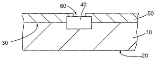
다음에 설명되는 도면들에서 동일한 구성요소들이 하나 이상의 도면에서 보여지는 경우에는 참조 번호들이 반복된다. 본 명세서에 개시된 예시적인 실시예에 대해 논의하기 전에, 통상적인 솔더 범프 금속화 설계의 구조 및 제조공정을 간략하게 살펴보는 것이 유용할 것이다. 이제 도면들을 참조하면, 특히 도1 내지 도5를 참조하면, 반도체 칩(10)의 표면 상에 전도성 솔더 범프를 형성하기 위한 통상적인 제조 공정이 도시되어 있다. 설명의 간략화를 위해서, 도1 내지 도5는 반도체 디바이스(10)의 상대적으로 작은 부분에 초점을 맞춘 것이다. 처음에 도1을 참조하면, 반도체 디바이스(10)는 대향하는 2개의 면(20, 30)을 포함한다. 상기 면(20)은 후면(backside)이라 종종 지칭되며 그리고 그 반대되는 면(30)은 전면(front side)이라 지칭된다. 활성 칩 회로들(미도시)은 상기 전면(30)에 인접한 하나 이상의 층들에 위치하는 것이 일반적이다. 본드 패드(40)는 상기 면(30)에 인접하여 제공되며 그리고 디바이스(10)의 회로에서부터 나중에 형성되는 솔더 범프를 통하는 전기적인 경로를 제공하도록 설계되는데, 이는 상기 디바이스(10)의 외부 회로와 전기적인 연결을 설립하기 위한 것이다. 디바이스(10)의 복잡도에 따라, 이러한 본드 패드들(40)이 수십개 존재할 수도 있다. 실리콘 질화물의 페시베이션층(50)이 상기 면(30) 상에 형성되며 그리고 패터닝되어 개구부(60)가 본드 패드(40) 쪽으로 형성된다. 페시베이션층(50)은 금속 물질이 반도체 디바이스(10)쪽으로 아래로 확산하는 것을 방지하도록 설계된다. Reference numerals are repeated when identical elements are shown in more than one figure in the figures described below. Before discussing the exemplary embodiments disclosed herein, it will be useful to briefly review the structure and fabrication process of a typical solder bump metallization design. Referring now to the drawings, and in particular with reference to FIGS. 1-5, a conventional manufacturing process for forming conductive solder bumps on the surface of
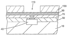
이제 도2를 참조하면, 페시베이션층(50), 본드 패드(40) 및 반도체 디바이스(10)로 구성된 적층 구조 위에 폴리이미드층(70)이 형성된다. 폴리이미드층(70)은 개구부(80)를 갖게 형성되며, 상기 개구부(80)는 페시베이션층(50)의 개구부(60)와 동일 중심을 갖게 위치된다. 구조적인 유연성 및 전기적 절연성이라는 2가지 장점을 제공할 수 있으므로 폴리이미드가 선택된다. 폴리이미드층(70)의 적용에 후속하여, 폴리이미드층(70) 위에 및 폴리이미드층의 개구부(80) 아래쪽으로 금속화층(90)이 형성되는바, 이는 본드 패드(40)와 오믹 콘택을 형성하기 위한 것이다. 이러한 금속화층(90)은 종종 언더 범프 금속화층 혹은 UBM 층 이라 지칭된다. UBM 층(90)은 종종 티타늄, 구리 및 니켈과 같은 상이한 금속 물질들의 순차적인 적층 형태로 형성된다. 도3에 도시된 바와 같이, 금속화층(90), 폴리이미드층(70), 페시베이션층(50), 본드 패드(40) 및 디바이스(10)로 구성된 스택 상에 절연 필름(100)이 형성된다. 절연 필름(100)에는 개구부(110)가 패터닝되는바, 상기 개구부(110)는 금속화층(90)의 일부를 노출시킨다. 상기 필름(100)은 마스크로서 기능하도록 설계되거나 혹은 스텐실 공정이 이용된다면 스텐실로 기능하도록 설계되는바, 이는 전도성 물질을 개구부(110) 내에 후속으로 형성하는 것을 가능케하며, 상기 전도성 물질은 결국에는 솔더 범프로 형성될 것이다. 상기 개구부(110)는 리소그래픽적인 패터닝 공정에 의해 형성되는 것이 일반적이다. Referring now to FIG. 2, a
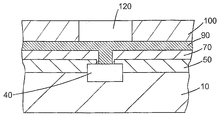
이제 도4를 참조하면, 반도체 디바이스(10)는 도금 공정을 경험하게 되는바, 따라서 전도성 물질(120)이 필름(100)의 개구부(110) 안에 및 금속화층(90)의 노출된 부분 상에 형성된다. 일반적으로, 상기 전도성 물질(120)을 땜납(solder 이하, 솔더)이며, 이는 금속화층(90)과 오믹 접촉을 형성한다. 통상적인 솔더는 주석-납(tin-lead) 혼합물로 구성된다. 최근의 동향은 주석-구리 솔더와 같은 무연-솔더에 관련된다. 폴리이미드층(70) 및 페시베이션층은 전도체(120) 및 금속화층(90)으로부터 디바이스(10)로의 물질의 확산을 금지한다. 본드 패드(40)는 도금에 의한 영향을 받지 않는다. Referring now to FIG. 4, the
도4에 도시된 필름(100)은 제거되며 그리고 도5에 도시된 바와 같이 열 리플로우 공정이 반도체 디바이스(10) 상에서 수행되는바 이는 전도체 물질(120)을 리플로우시켜 동그란 범프를 형성하기 위한 것이다. 솔더 리플로우 공정에 후속하여, 솔더 범프(120)의 측면에 있는 금속화층(90)의 일부분들이 습식 식각에 의해서 제거된다. 이 시점에서, 솔더 범프(120), 금속화층(90) 및 그 하부의 범프 패드(40) 사이에 오믹 경로가 존재한다. 페시베이션층(50)과 폴리이미드층(70)은 그대로 남아있는다. The
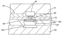
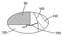
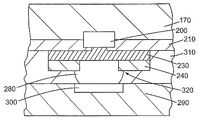
배경기술 부분에서 언급한 바와 같이, 금속화층(90) 아래에 폴리이미드층(70)을 배치하는 것은, 중대한 결과를 가져오는바, 이러한 결과는 반도체 디바이스(10)가 또 다른 디바이스 상에 플립-칩 마운트되는 때에 명백해진다. 이에 관하여, 도6에는 상기 면(30)이 아래를 향하도록 또 다른 기판(130) 상에 플립-칩 마운트된 반도체 디바이스(10)의 단면이 도시되어 있다. 전기 디바이스(130)와 반도체 디바이스(10)의 열 팽창 계수의 차이로 인한 스트레스를 완화시키기 위해서, 폴리이미드층(70)과 기판(130) 사이에는 언더필(underfill) 물질(140)이 배치된다. 반도체 디바이스(10)의 솔더 범프는 상기 디바이스(130)의 대응 본드 패드(150) 상에 위치한다. 이러한 방식으로, 금속화층(90) 및 솔더 범프(120)를 통하여 디바이스(10)의 본드 패드(40)와 디바이스(130)의 본드 패드(150) 사이에 전기적인 경로가 확립된다. 솔더 범프(120), 언더필 층(140) 및 금속화층(90)의 작은 부분이 작은 타원(160)으로 표시된다. 타원(160)으로 표시된 부분은 도7에서 확대되어 표현된다. As mentioned in the background section, disposing the
도7은 도6에 도시된 바와 같이 금속화층(90)과 솔더 범프(120) 사이에 폴리이미드층(70)을 배치하는 경우의 단점을 예시한다. 솔더 범프(120)에서 도시된 크랙은, 언더필 물질(140)과의 경계선(165)으로부터 솔더 범프(120)의 중앙 부분을 향해 연장된다. 상기 크랙(160)은 적절히 보상되지 못한 열 스트레스의 결과물인바, 상기 열 스트레스는 무연 솔더 범프(120)의 상당한 강성(stiffness) 및 크랙(160)이 발생한 영역으로부터 폴리이미드층(70)까지의 상당한 거리로 인해, 적절히 보상되지 못한다. 상기 크랙(160)은 솔더 범프(120)의 전체 폭을 가로질러 전파될 수도 있으며 그리고 개방 회로(open circuit)를 야기할 수도 있다. FIG. 7 illustrates the disadvantages of disposing the
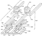
이제, 전술한 바와 같은 종래 공정의 단점을 극복할 수 있는 신규한 제조 공정의 일례가 도8 내지 도12를 참조하여 이해될 것인바, 도8 내지 도12는 솔더 범프의 형성을 가져오는 다양한 공정 단계들이 진행되는 집적회로 혹은 반도체 디바이스(170)의 단면을 연속적으로 도시한 도면들이다. 도8 내지 도12는 디바이스(170)의 작은 일부분만을 도시한 도면들이라는 점을 유의해야 한다. 반도체 디바이스(170)는 가령, 마이크로프로세서, 그래픽 프로세서, ASIC, 메모리 디바이스 등등과 같이 전자 분야에서 이용되는 수 많은 유형의 회로 디바이스들 중 임의의 것이 될 수 있으며 그리고 싱글 코어 혹은 멀티-코어가 될 수도 있다. Now, an example of a novel manufacturing process that can overcome the shortcomings of the conventional process as described above will be understood with reference to FIGS. 8 to 12, which show various processes resulting in the formation of solder bumps. Continuously showing cross-sections of an integrated circuit or
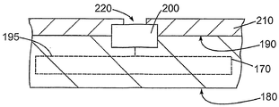
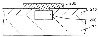
구조적으로 말해서, 디바이스(170)는 서로 대향하는 면들 즉, 180과 190을 갖는다. 점선 박스(195)로 도식적을 표현되는 디바이스 회로는 상기 면(190)에 인접하여 위치할 수도 있다. 상기 회로(195)를 외부 디바이스에 전기적으로 연결하기 위해서, 반도체 디바이스(170)에는 다수개의 전도체들 혹은 본드 패드들이 제공될 수 있는바, 이러한 것들 중 하나가 도면부호 200으로 도시되어 있으며 그리고 면(190)에 근접하여 위치하고 있다. 반도체 디바이스(170)의 복잡도 및 사이즈에 따라 수십 개의 패드(200)들이 존재할 수도 있다. 본드 패드(200)는 알루미늄, 구리, 은, 티타늄, 내열성 금속(refractory metal), 내열성 금속 화합물, 및 이들의 합금 등등과 같은 다양한 전도성 물질들로 이루어질 수 있다. 본드 패드(200)는 도금법, 물리기상증착(PVD) 혹은 또 다른 증착 기법들에 의해서 형성될 수 있다. Structurally speaking,
페시베이션층(210)은 면(190) 상에 형성되며 그리고 개구부(220)를 갖는다. 페시베이션층(210)은 금속류 혹은 다른 종류의 물질이 반도체 디바이스(170)쪽으로 아래로 확산하는 것을 방지하도록 설계된다. 상기 페시베이션층(210)은 예컨대, 실리콘 질화물, 실리콘 이산화물, 다양한 규산염 유리(silicate glass)들 등등과 같은 다양한 절연 물질들로 구성될 수 있다. 상기 개구부(220)는 잘 알려진 리소그래픽적 패터닝 공정 및 식각 공정에 의해 형성될 수 있다.
설명의 간략화를 위해서, 나머지 도면들에는 회로(195)가 포함되지 않는다. 이제 도9를 참조하자. 전도체 혹은 금속층(230)이 페시베이션층(210) 위에 그리고 개구부(220) 내에 형성되므로, 본드 패드(200)와의 오믹 컨택이 확립된다. 금속화층(230)은 본드 패드(200)와 후속으로 형성될 솔더 구조(미도시) 사이에서 전도성 인터페이스를 제공하도록 설계된다. 금속화층(230)은 예컨대, 알루미늄, 구리, 은, 금, 티타늄, 내열성 금속, 내열성 금속 화합물, 혹은 이들의 합금 등등과 같은 다양한 전도성 물질들로 구성될 수 있다.For simplicity of explanation, the
일원화된 구조 대신에, 상기 금속화층(230)은 티타늄층 다음에 니켈-바나듐층 그 다음에 구리층이 뒤따르는 것과 같은, 다수의 금속층들의 라미네이트(laminate)로 구성될 수도 있다. 본 발명의 다른 실시예에서는, 티타늄층은 구리층으로 커버될 수 있으며 뒤이어 니켈로 탑 코팅될 수 있다. 하지만, 해당 기술분야의 당업자라면, 매우 다양한 전도성 물질들이 금속화층(230)으로 이용될 수 있다는 점을 능히 이해할 것이다. 금속 물질을 적용하기 위한 공지된 다양한 기법들, 가령, 물리기상증착(PVD), 화학기상증착(CVD), 도금(plating) 등등이 이용될 수 있다. 금속층(230)과 전도성 패드(200) 사이에 추가적인 전도체 구조물들이 개재될 수도 있음을 유의해야 한다. Instead of a unitary structure, the
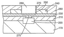
금속화층(230), 페시베이션층(210), 패드(200) 및 반도체 디바이스(170)로 구성된 적층구조 상에 절연 필름(240)이 형성된다. 절연 필름(240)은 금속층(230)의 표면(255) 상에 위치한다. 상기 절연 필름(240)은 반도체 디바이스(170), 금속화층(230) 및 후속으로 형성될 솔더 범프(미도시)의 열 팽창에 있어서의 차이들에 대해 페시베이션 및 완충(cushion)을 제공하기 위한 것이다. 절연층(240)의 예시적인 물질로는 예컨대, 폴리이미드, 벤조시클로부텐(benzocyclobutene) 등등과 같은 폴리머 물질(polymeric material)을 포함할 수 있으며 혹은 실리콘 질화물 등과 같은 또 다른 절연 물질을 포함할 수도 있다. 스핀 코팅, 화학기상증착 혹은 다른 증착 공정이 이용될 수 있다. 절연층(240)은 개구부(250)를 갖게끔 리소그래픽적으로 패터닝되며, 상기 개구부(250)는 금속화층(230)의 일부를 노출시킨다. 절연층(240)은 금속화층(230) 위에 위치함을 유의해야 하는바, 이는 도1 내지 도5에 도시된 종래기술에서 금속화층(90)의 아래에 있는 것과는 반대이다. 이러한 배치는 구조적인 장점들을 제공하는데, 이에 대해서는 상세히 후술될 것이다. An insulating
이제 도10을 참조하자. 절연층(240), 금속화층(230), 페시베이션층(210), 패드(200) 및 반도체 디바이스(170)로 구성된 적층구조 상에 마스크 필름(260)이 형성된다. 마스크 필름(260)은 개구부(270)를 갖게 리소그래픽적으로 패터닝되는바, 상기 개구부(270)는 절연층(240)의 개구부(250)와 동일중심을 갖는다. 또한, 상기 개구부(270)와 개구부(250)는 금속화층(230)의 표면(255)의 소정 부분(275)을 노출시킨다. 후속 공정에서, 전도성 물질이 개구부(250)와 개구부(270) 내에 형성되어, 금속화층(230) 및 그 아래에 있는 디바이스(170)의 본드 패드(200)와 오믹 콘택을 확립한다. 마스크 필름(260)은 예를 들면, 페놀 수지로 고무를 입힌 에폭시 수지(rubberized epoxy resin phenol resin), 용융 실리카(fused silica), 및 합성 고무(synthetic rubber)로 만들어질 수 있다. 선택적으로는, 금속 적용 마스크로 적절한 다른 물질들이 이용될 수도 있다. Reference is now made to FIG. 10. The
도11에 도시된 바와 같이, 반도체 디바이스(170)에 도금 공정을 적용하여, 상기 개구부(270)와 개구부(250) 내에 그리고 금속화층(230)의 표면(255)의 노출된 소정 부분(275) 상에 전도성 물질(280)을 증착한다. 마스크 필름(260)은 이러한 증착 공정에 대한 마스크로서 기능한다. 전도체(280)는 납-기반의 솔더 혹은 필요에 따라 무연 솔더가 될 수도 있다. 예시적인 물질들은 예컨대, 주석-구리(tin-copper), 주석-은(tin-silver), 혹은 다른 솔더 물질들을 포함한다. 전도성 물질(280)은 상기 절연층(240)과 경계를 이룬다. 이 시점에서, 본드 패드(200), 금속화층(230), 및 전도성 물질(280) 사이에는 전도성 경로가 존재한다. 페시베이션층(210)은 영향을 받지 않는다. 물론, 다른 전도체(들)(미도시)이 전도체(280)와 본드 패드(200) 사이에 위치할 수도 있으며 그리고 원하는 오믹 경로를 여전히 제공할 수 있다. As shown in FIG. 11, a plating process is applied to the
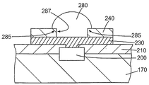
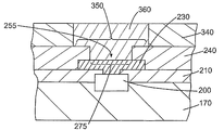
도12에 도시된 바와 같이, 도11에 도시된 마스크 필름(260)은 제거되며, 그리고 리플로우 공정이 수행되어 전도체(280)를 공 모양 혹은 범프-유사 구조로 리플로우 시킨다. 예시적인 실시예에서, 반도체 디바이스(170)는 약 170 ~ 190℃ 로 약 10 ~ 120 초 동안 가열될 수 있다. 리플로우 공정을 위한 적절한 파라미터들은 전도체 물질(280)의 조성에 따라 달라질 것이다. 금속화층(230)의 원하지 않는 부분들은 화학 식각 공정에 의해서 제거된다. 따라서, 전도체(280)에 대해 측면인 페시베이션층(210)의 소정 부분들이 노출된다. 전도체(280)와 범프 본드 패드(200) 사이에는 금속화층(230)을 통한 전도성 경로가 존재한다. 전도체(280)가 절연층(240)의 소정 부분(285) 상에 위치함을 주목하라. 상기 부분(285)은 전도체(280)의 주변 코너(287)와의 스트레스 감소 경계를 제공한다. As shown in FIG. 12, the
절연층(240)의 새로운 배치로 인한 장점들은 디바이스(170)가 또 다른 기판에 마운트되는 경우 자명해진다. 이제, 반도체 디바이스(170)가 또 다른 전기 디바이스(290) 상에 마운트된 것을 도시하고 있는 도13을 참조하자. 상기 전기 디바이스(290)는 인쇄회로기판이 될 수도 있으며 혹은 임의의 다른 전자 디바이스가 될 수도 있다. 도13은 디바이스(170)가 뒤집혀서 전자 디바이스(290) 위에 마운트되어 있는 플립-칩 마운팅 구조를 도시한 것으로, 따라서 솔더 구조(280)는 전자 디바이스(290)의 본드 패드(300) 상에 놓여진다. 상기 디바이스(290)는, 디바이스(170)의 대응 범프들(280)을 받아들이기 위해 이러한 패드(300)들을 다수개 포함할 수도 있다는 점을 유의해야 한다. 필요하다면, 후속 리플로우 공정에서 솔더 구조(280)와 함께 혼합되도록 된 작은 솔더 범프들(미도시)이 상기 패드(300)에 제공될 수도 있다. 디바이스(170)와 디바이스(290) 사이에 언더필 물질(310)이 분산되는바, 이는 디바이스(170)와 디바이스(290)의 열 팽창 계수의 차이로 인한 효과를 감소키기 위한 것이다. 상기 언더필 물질(310)은 예컨대, 실리카 충전물 및 페놀 수지와 혼합된 에폭시 수지가 될 수도 있다. 금속화층(230)과 솔더 구조(280) 사이에 절연층(240)이 위치하기 때문에, 열(thermal) 스트레스 및 도6 및 도7에 도시된 종래기술과 관련된 크랙킹에 대해서 추가적인 완충 효과가 솔더 범프(280)의 코너(320)에 제공된다. 상기 코너(320)는 솔더 구조(280)의 주변부 전체를 따라 연장된다는 점을 주목해야 한다. The advantages of the new placement of the insulating
전술한 예시적인 실시예에서는, 솔더 구조(280)를 형성하기 위해서 도금 공정이 이용될 수도 있다. 도14 내지 도18에 도시된 대안적인 공정예에서는, 스텐실 공정이 이용되어 솔더 구조를 형성할 수도 있다. 처음에 도14를 참조하면, 반도체 디바이스(170)는 본 명세서에서 앞서 전술한 바와 같이 공정처리되어 본드 패드(200), 페시베이션층(210) 및 금속화층(230)이 제공된다. 이 단계에서, 레지스트 혹은 다른 마스크 물질로 구성된 식각 마스크(330)가 금속화층(230) 상에 형성된다. 이후, 식각 공정이 금속화층(230)에 대해 수행되어 본드 패드(200) 측면의 금속화층의 소정 부분들이 제거되며 그리고 도15에 도시된 바와 같이 페시베이션층(210)의 일부분을 노출시킨다. 상기 식각 마스크(330)는 애싱(ashing), 솔벤트 스트리핑 등등에 의해 제거될 수도 있다. 위에서 바라보았을 때, 금속화층(230)은 원형 혹은 원하는 형태를 가질 수 있다. 본드 패드(200)는 상기 식각 혹은 마스크 스트립에 의한 영향을 받지 않는다. In the exemplary embodiment described above, a plating process may be used to form the
도16에 도시된 바와 같이, 금속화층(230), 페시베이션층(210), 패드(200) 및 반도체 디바이스(170)로 구성된 적층구조 상에 절연층(240)이 형성되는바, 이는 본 명세서에서 통상적으로 언급된 바와 같다. 절연층(240)은 금속화층(230)에까지 도달하는 전술한 개구부(250)를 가지며, 상기 개구부(250)는 금속화층의 표면(255) 중 일부(275)를 노출시킨다. As shown in FIG. 16, an insulating
이제 도17을 참조하면, 절연층(240), 금속화층(230), 페시베이션층(210), 패드(200) 및 반도체 디바이스(170)로 구성된 적층구조 상에 스텐실(stencil)(304)이 형성된다. 스텐실(340)은 금속화층(230) 및 절연층(240)의 소정 부분들 상에 형성된 개구부(350)를 포함한다. 스텐실(340)은 예를 들면, 페놀 수지로 고무를 입힌 에폭시 수지(rubberized epoxy resin phenol resin), 용융 실리카, 및 합성 고무로 만들어질 수 있다. 선택적으로는, 금속 적용 스텐실을 위해 적절한 다른 물질들이 이용될 수도 있다. 전도체 페이스트(360)가 스텐실(340)의 상기 개구부(350) 안으로 프레스된다. 전도체 페이스트(360)는 금속층(230)의 표면(255)의 노출된 부분(275) 및 절연층(240)의 소정 부분(365) 상에 위치된다. 전도체 페이스트(360)는 앞서 설명된 솔더 범프(280)를 위해 이용된 것과 동일한 물질로 구성될 수도 있다. 물론, 다른 전도체(들)(미도시)이 전도체(360)와 본드 패드(200) 사이에 위치할 수도 있으며 그리고 원하는 오믹 경로를 여전히 제공할 수 있다. Referring now to FIG. 17, a stencil 304 is formed on a stack structure consisting of an insulating
공정을 완료하기 위하여, 스텐실(340)은 제거되며 그리고 열 리플로우 공정이 수행되어 전도체 페이스트를 범프로 재형상화하는바, 이는 도18에 도시된 바와 같이 패드(200)에 야금학적으로 결합한다. 예시적인 실시예에서, 반도체 디바이스(170)는 약 170 ~ 190℃ 로 약 10 ~ 120 초 동안 가열될 수 있다. 리플로우 공정을 위한 적절한 파라미터들은 전도체 페이스트(360)의 조성에 따라 달라질 것이다. 상기 페시베이션층(210)은 영향을 받지 않는다. 전도체(360)는 절연층(240)의 소정 부분(365) 상에 위치된다. 앞서 설명된 실시예처럼, 절연층(240)은 솔더 범프(360)의 주변 코너들(370)를 위한 향상된 구조적인 보호를 제공한다. To complete the process, the
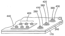
본 명세서에 개시된 바와 같이 절연층(240)을 배치하는 것은, 솔더 범프들(280, 360) 등등에 대해서 향상된 구조적인 보호를 제공할 수 있을 뿐만 아니라, 상기 언더 범프 금속화층(230)이 전기적인 라우팅 구조로서 기능하는 것을 가능케한다. 이제 도19를 참조하면 예시적인 실시예가 이해될 것인바, 도19는 절연층(240)과 위쪽으로 향해있는 다수의 범프들을 구비한 반도체 디바이스(170)의 일부에 대한 도면이다. 상기 범프들 중 하나는 도8 내지 도12에서 도면부호 280으로 지칭된다. 다른 2개의 범프들은 각각 380, 390으로 지칭된다. 6개의 범프들의 그룹은 총체적으로 도면부호 400으로 표시된다. 상기 범프들(280, 380, 390)에는 별개의 언더 범프 전도체 구조들 혹은 금속층들(410, 420, 430)이 제공될 수 있는바, 이들은 본 명세서에 개시된 기법들을 이용하여 구조적으로 격리된다. 상기 금속층들(410, 420, 430)은 절연층(240)에 의해 커버되며 따라서 점선으로 투명하게 도시된다. 범프들의 그룹(400)은 본 명세서에 개시된 기술들을 이용하여 형성될 수 있지만, 공통 언더 범프 전도체 구조 혹은 금속층(440)을 갖게 형성되며, 상기 공통 언더 범프 전도체 구조 혹은 금속층(440) 역시도 절연층(240)에 의해 커버되므로, 이 역시 점선으로 투명하게 도시된다. 따라서, 절연층(240)은 다수의 개구부들을 갖게 형성되는바, 이는 범프들(400)을 형성하기 전에 금속층(440)의 디수의 부분들을 노출하기 위함이다. 이러한 방식으로, 금속층(440)은 범프들의 그룹(400)을 위한 라우팅 구조로서 기능할 수 있다. 이러한 점은, 전원 혹은 접지와 같은 소정 유형의 입력/출력에 다수의 범프들이 일시적으로 혹은 영구적으로 전용되는 경우에 있어 유용할 것이다. 범프들의 그룹(400)과 금속화층(440) 사이에 절연층(240)이 위치하고 있기 때문에, 리플로우 동안에 솔더가 옆으로 스며들어 원하지 않는 단락(short)을 야기하는 위험 없이, 선택된 범프들이 함께 그룹화될 수 있다. 물론, 범프들의 개수 및 범프들을 그룹화하는 것 그리고 공통의 언더 범프 금속화층(440)의 형상은 매우 다양할 수 있다. Placing insulating
해당 기술분야의 당업자라면, 본 명세서에 개시된 예시적인 공정들이, 웨이퍼에 배치된 다수개의 다이들에 대해 동시에 수행될 수도 있다는 점을 능히 이해할 것이다. 이후 단일화 공정이 실행될 수 있다. 대안적으로는 단일화 공정 이후에 개별 다이들이 공정처리될 수도 있다. Those skilled in the art will appreciate that the exemplary processes disclosed herein may be performed simultaneously on multiple dies placed on a wafer. A singulation process can then be performed. Alternatively, individual dies may be processed after the singulation process.
반도체 디바이스(170)는 다양한 방식으로 마운트될 수 있다. 도20은 몇몇개의 예시적인 마운팅 가능성을 도시한 분해도이다. 도시된 반도체 디바이스(170)는 위로 향하고 있는 솔더 범프들(280)을 구비한다. 상기 디바이스(170)는 화살표(450)로 도시된 것처럼 뒤집혀질 수 있으며(flipped over) 그리고 기판(460) 상에 플립-칩 마운트될 수도 있다. 상기 기판(460)은 패키지 기판, 인쇄회로기판 혹은 다른 유형의 기판이 될 수 있다. 패키지 기판으로 구성되는 경우, 상기 기판(460)은 핀 그리드 어레이, 볼 그리드 어레이, 랜드 그리드 어레이, 표면 실장(surface mount) 혹은 다른 유형의 구성이 될 수 있다. 상기 기판(460)은 또 다른 기판(470) 상에 마운트될 수도 있다. 기판(470)은 인쇄회로기판, 혹은 다른 유형의 기판이 될 수 있다. 예를 들어, 기판(470)은 컴퓨터 시스템의 마더보드가 될 수도 있다. 반도체 디바이스(170)는 가령, 대쉬 박스 480로 표현되는 컴퓨팅 디바이스와 같은 더 큰 시스템 내에 포함될 수도 있다. 컴퓨팅 디바이스(480)는 예컨대, 디지털 TV, 휴대용 모바일 디바이스, 퍼스널 컴퓨터, 서버, 메모리 디바이스, 그래픽 카드와 같은 애드-인 보드(add-in board), 혹은 반도체를 채용하는 다른 임의의 컴퓨팅 디바이스에 포함될 수 있다. The
앞서 논의된 도19는 전기적인 라우팅을 위한 UBM 구조의 예시적인 이용예를 도시하였다. UBM 배치를 이용한 복잡한 라우팅의 몇몇 사례들이 도23 내지 도30에 도시된다. 이들 도면들을 논의하기 전에, 입력/출력을 위해 솔더 구조들을 활용하는 종래의 통상적인 전기 라우팅 설계를 간략히 살펴보는 것이 유용할 것이다. 도21은, 바닥면이 위로 향하게 즉, 다수의 전도체 볼들이 보여지게 위치한 통상적인 반도체 칩(500)의 일례를 예시한 도면이다. 이들 볼들 중 2개는 도면부호 510과 515로 표시된다. 인쇄회로기판(미도시)에 마운팅시키는 동아느, 상기 칩(500)은 뒤집혀지며 따라서 볼(510, 515 등등)은 아래를 향하게 되어 인쇄회로기판 상의 대응 솔더 구조들과 야금학적 연결을 확립한다. 솔더 볼들(510, 515 등)은 칩(500)의 몸체 내의 다양한 회로 구조체들에 상호연결되는바, 상기 회로 구조체들은 도21에 도시되어 있지 않다. 하지만, 솔더 볼(510, 515 등)과 칩(500) 내의 회로 구조체들 사이의 몇몇 예시적인 상호연결 구조들이 도22에 상세히 도시되어 있다. 19 discussed above illustrates an example use of the UBM structure for electrical routing. Some examples of complex routing using UBM deployment are shown in FIGS. 23-30. Before discussing these figures, it would be useful to briefly review a conventional conventional electrical routing design that utilizes solder structures for input / output. 21 is a diagram illustrating an example of a
이제 도22를 참조하면, 도22에는 도21에 도시된 2개의 솔더 볼(510, 515)이 도시되어 있을 뿐만 아니라, 솔더 볼(510, 515)로부터 칩(500) 내의 통상적인 2개의 전자 디바이스들(520, 525)까지 아래로 연장된 전형적인 상호연결 구조들이 도시되어 있다. 다음과 같은 점이 이해되어야 하는바, 솔더 볼(510, 515)과 전자 디바이스들(520, 525) 사이의 영역(527)에 존재하는 다양한 절연층들은 도시되어 있지 않으며, 따라서 솔더 볼(510, 515)과 전자 디바이스들(520, 525) 사이의 전기적 상호연결 구조들의 세부사항들이 명확히 도시되어 있다. 상기 전자 디바이스들(520, 525)은 게이트(530)와 게이트(535)를 각각 갖는 전계 효과 트랜지스터들로서 예시된다. 2개의 금속화층들(540, 545) 및 재분배층(redistribution layer : RDL)(550)이 솔더 볼(510, 515)과 전자 디바이스들(520, 525) 사이에 개재된다. 금속화층(540)은 다수개의 금속 라인들로 구성되는데, 이들 중 2개가 도시되어 있으며 도면부호 555와 560으로 표시된다. 이와 유사하게 금속화층(545)은 다수개의 금속 라인들로 구성되는데, 이들 중 2개가 도시되어 있으며 도면부호 565와 567로 표시된다. 그리고 RDL(550)은 다수개의 금속 라인들로 구성되며, 이들 중 2개가 도면부호 570과 575로 표시된다. 금속 라인(555)은 콘택(580)을 통해 디바이스(520)의 게이트(530)에 전기적으로 연결된다. 금속 라인들(555, 565)은 비아(585)에 의해서 전기적으로 서로 연결되며 그리고 RDL 구조(570)는 비아(590)를 통해서 금속 라인(565)에 전기적으로 연결된다. 디바이스(525)의 게이트(535)에 RDL 구조(575)를 전기적으로 링크시키기 위해서, 콘택(595)과 2개의 비아(600, 605)들이 제공된다. 솔더 볼(510, 515)들은, 각각의 UBM 볼 혹은 본드 패드(610, 615) 및 전도체 확장부(617, 619)에 의해서, 각각의 RDL 구조들(570, 575)에 전기적으로 연결된다. Referring now to FIG. 22, in addition to the two
상기 RDL(550)는, 솔더 볼(510, 515) 뿐만 아니라 도1에 도시된 다른 솔더 볼들을 위한 라우팅 및 레이아웃에서 여분의 유연성을 제공하도록 설계된다. 솔더 볼들은 초기 오정렬 혹은 유출(spill over)과 그 결과로서 리플로우 공정에서 야기되는 회로 단락이라는 소정의 위험을 갖고 제조되는 것이 일반적이기 때문에, RDL(550)의 RDL 구조들(570, 575) 사이에서 소정의 최소 피치값 X1 이 유지되어야만 하는데, 이는 교차 오염 및 회로 단락의 가능성을 감소시키기 위한 것이다. The
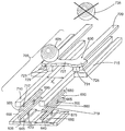
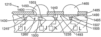
이제, 복잡한 라우팅을 위해서 UBM 층을 적용하는 반도체 칩 혹은 디바이스에 대한 예시적인 실시예가 도23 및 도24를 참조하여 이해될 것이다. 도23은 반도체 칩 혹은 디바이스(620)에 대한 예시적인 실시예를 도시한 도면으로, 상기 반도체 칩(620)은 다수의 솔더 구조들이 보여지도록 바닥면이 위로 향하게 도시되어 있으며, 상기 다수의 솔더 구조들 중 2개는 도면부호 623과 625로 표시된다. 상기 칩(620)은 수십, 수백 혹은 수천개의 솔더 구조들을 포함할 수 있다. 하지만, 간략히 예시하기 위해서, 도23에는 몇몇개의 솔더 구조들만이 도시되어 있다. 도면부호 630으로 표시된 위치에는 그 어떤 솔더 볼들도 존재하지 않음을 주목하라. 이러한 생략의 중요성은 도24를 참조하여 후술될 것이다. 반도체 디바이스(620)는 가령, 마이크로프로세서, 그래픽 프로세서, ASIC, 메모리 디바이스 등등과 같이 전자 분야에서 이용되는 수 많은 유형의 회로 디바이스들 중 임의의 것이 될 수 있으며 그리고 싱글 코어 혹은 멀티-코어가 될 수도 있다. An exemplary embodiment of a semiconductor chip or device that applies a UBM layer for complex routing will now be understood with reference to FIGS. 23 and 24. FIG. 23 illustrates an exemplary embodiment of a semiconductor chip or
이제 도24를 참조하면, 도24는 솔더 구조(625)와 도23에 도시된 반도체 칩(620)의 상기 위치(630) 둘다를 좀더 확대한 도면이다. 수백만개일 수도 있는 반도체 칩(620) 내의 회로 디바이스들 중 2개가 도24에 도시되어 있으며, 도면부호 635, 640으로 각각 표시된다. 회로 디바이스(635, 640)는 전계 효과 트랜지스터로서 예시되어 있지만, 이들은 집적회로에서 이용되는 다양한 회로 디바이스들 중 임의의 것이 될 수도 있다. 트랜지스터(635, 640)들은 게이트(645, 650)를 각각 가지며, 이들 게이트들은 콘택(670, 675)에 의해서 금속화층(665)의 금속 라인(655, 660)에 각각 연결된다. 제 2 금속화층(680)은 금속 라인들(685, 690)로 구성되며, 금속 라인들(685, 690)은 비아(695, 700)에 의해서 금속 라인(655, 665)에 각각 연결된다. 비록, 2개의 금속화층(665, 680)만이 도시되어 있지만, 반도체 칩(620)의 복잡도에 따라, 더 많은 금속화층이 존재할 수도 있다. Referring now to FIG. 24, FIG. 24 is an enlarged view of both the
다수개의 RDL 구조들로 구성된(이들 중 2개는 도면부호 710, 715로 표시됨) RDL(705)이 제공되는바, 이는 솔더 볼(623)(도23 참조)과 솔더 볼(625) 및 그 하부의 회로 디바이스들 사이에서 전기적인 라우팅을 설립하기 위한 것이다. RDL(705)은 많은 전도체 라인들로 구성되는 것이 바람직하며, 상기 전도체 라인들은 상대적으로 큰 사이즈 및/또는 바람직하게는 낮은 오믹 손실을 제공하는 다른 특징들을 갖게 제조되는 것이 바람직하다. RDL(710) 구조는 비아(717)에 의해서 금속 라인(685)에 연결되며 그리고 RDL(715) 구조는 비아(719)에 의해서 금속 라인(690)에 연결된다. 바로 이 지점까지는, 도24에 도시된 구조와 도22에 도시된 종래기술에 따른 솔더 볼 및 전기적 라우팅 구조는 거의 흡사하다. 하지만, 예시된 상기 실시에에서는, 전도체 혹은 UBM 구조(720)(이는 훨씬 더 광범한 UBM 층의 일부가 될 수도 있다)가, 솔더 볼(625)과 RDL 구조들(710, 715) 사이에 개재되며 그리고 전기적으로 연결된다. 상기 UBM 구조는 패드들 혹은 사이트(723, 725)들을 포함하는바, 사이트(723, 725)들은 교차-부재(cross-member)(727)에 의해서 함께 결합되며 그리고 2개의 확장 부재(729, 731)에 의해서 RDL 구조(710, 715)에 각각 연결된다. 이와 같은 방식으로, 패드 RDL 구조(715)에 대해 입력/출력을 제공하기 위하여 패드(725) 상의 상기 지점(630)에 배치되어야만 했던 솔더 볼(735)이, 제거될 수 있다. 솔더 볼(735)이 제거될 수 있기 때문에, RDL 구조(710)와 RDL 구조(715)는 최소 피치값 X2 를 갖게끔 좀더 좁혀질 수 있으며, 상기 최소 피치값 X2 는 도22에 도시된 종래 구조의 최소 피치값 X1 보다 더 작을 수 있다. UBM 구조(720)의 패드 사이트들(723, 725)은 트랜지스터(635, 640)의 게이트들(645, 650)에 공통으로 연결된다. 따라서, 상기 UBM 구조(720)는 예컨대, 전원 신호, 접지 신호 혹은 소정의 경우에 따른 신호와 같은, 동일한 유형의 전기 신호에 전용되는 볼/범프 사이트들을 공통으로 결합시키기 위해 이용되어야만 한다. 비록, UBM 구조(720)가 단순한 말발굽 모양의 디바이스로서 예시되어 있지만, 상기 UBM 구조(720)는 매우 다양한 구성을 가질 수 있다는 점을 유의해야 하며 그리고 도23의 반도체 칩(620) 상에 도시된 다양한 전도체 범프들을 다양한 방식으로 결합시킬 수 있는 많은 수의 유사한 UBM 구조들을 동반할 수도 있다는 점을 유의해야 한다. 또한, 상기 UBM 구조(720)는 본 명세서에서 설명된 기법들 및 물질들을 이용하여 제조될 수 있다는 점을 유의해야 한다.An
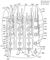
이제 도25를 참조하면, 도25에는 도23에 도시된 반도체 칩(620)의 작은 부분이 도시되어 있으며 그리고 상기 칩(620)으로부터 분해된 소수의 솔더 볼들(740, 745, 750, 755, 760)이 도시되어 있다. 반도체 칩(620)의 수 많은 종류의 내부 회로 구조들 중 몇몇 개가 점선 박스 A, B, C, D, E, F, G, H 로 표시된다. 상기 회로 구조들 A, B, C, D, E, F, G, H 는, 예컨대, 전력 레일(power rail), 접지 레일(ground rail), 캐패시터, 집적회로 기능블록, 메모리 디바이스, 프로세서 코어 혹은 반도체 칩에서 실제로 이용되는 임의의 것들이 될 수 있다. 회로구조 A, B, C, D, E, F, G, 및 H는 화살표 라인으로 도식적으로 표현된 각각의 배선들(805, 810, 815, 820, 825, 830, 835, 840)에 의해서, 각각의 RDL 구조(765, 770, 775, 780, 785, 790, 795, 800)에 전기적으로 연결된다. 상기 배선들(805, 810, 815, 820, 825, 830, 835, 840)은, 도24에 도시된 바와 같은 다중 금속화층(665, 680)과 같은 하나 이상의 금속화층 혹은 다른 전도성층들로 구성될 수 있다. 전도체 패드(845, 850, 855, 860)는 RDL 구조(770, 780, 790, 800)에 각각 연결된다. 솔더 볼들(745, 750, 755, 760)은 전도체 패드(845, 850, 855, 860)에 마운트된다. Referring now to FIG. 25, FIG. 25 shows a small portion of the
전도체 패드(865, 870, 875, 880)는 RDL 구조(765, 775, 785, 795)에 각각 연결된다. 전도체 패드(865, 870, 875, 880)는 전기적으로 함께 결합되며 그리고 UBM 구조(885)의 일부로서 제작되는바, 이는 그리드-유사(grid-like) 구조를 형성한다. UBM 구조(885)는 각각의 연장부에 의해서 하부의 RDL 구조(765, 775, 785, 795)에 연결될 수 있으며, 이들 중 하나가 패드 사이트(865) 인근에 도시되어 있으며 도면부호 890으로 표시된다. 사실, 패드들(845, 850, 855, 860)은 도시되지 않은, 유사한 확장부들을 이용할 수도 있다. 솔더 볼(740)은 패드(865)에서 UBM 구조(885)에 연결된다. 이러한 방식으로 솔더 볼(740)을 통한 전기적 입력/출력이 본드 패드들(865, 870, 875, 880) 모두에 대해 제공되며 따라서 그 하부의 회로 구조들(A, C, D, F)에게도 제공된다. UBM 구조(885)를 위한 그리드-유사 구조는 상대적으로 간단한 레이아웃이라는 장점을 갖는바, 이는 용이하게 리소그래픽적으로 패터닝될 수 있으며 공지된 기술들을 이용하여 용이하게 형성될 수 있다. 또한, 이러한 구조는 비교적 효율적으로 전류를 전달할 수 있으며 따라서 오믹 손실이 작아질 수 있다. 전도체 패드들(865, 870, 875, 880) 모두가 공통적으로 연결되며 그리고 UBM 구조(885)의 일부이기 때문에, 이들 본드 패드들은 접지, 전원 혹은 신호와 같은 특정 유형의 전기적 입력/출력에 전용될 수 있다. 다른 패드들(845, 850, 855, 860)은 전원, 접지 혹은 필요에 따라 신호를 위한 입력/출력으로 연결될 수도 있다. 물론, 모든 패드들(845, 850, 855, 860, 865, 870, 875, 880)은 제조의 단순화를 위해서 동일 평면 상에 제조될 수도 있다.
상기 UBM 구조(885)는 통상적으로 패드(870, 875, 880)에 위치되어야만 했던 솔더 볼들의 제거를 가능케 한다. 따라서, 나머지 솔더 볼들(740, 745, 750, 755, 760)의 전체 배치가 조밀해질 수 있다. The
개시된 UBM 구조에 따르면 이용가능한 잠재적인 라우팅에 관한 상당한 유연성이 예상될 수 있다. 이제 도26을 참조하면, 도26은 칩(620)의 작은 부분을 도시한 평면도이다. 도26에는 3개의 그리드-타입 UBM 구조들(915, 920, 925)(이들은 더 큰 확장형 UBM 층의 일부가 될 수도 있다)이 도시되어 있는바, 설명의 간략화를 위해서 이들 UBM 구조들 주위에 형성된 절연 물질들은 도시되지 않았다. 먼저, UBM 구조(915)에 관련된 부분을 살펴보면, 전도체 패드(930, 935, 940, 945)가 도시되어 있는바, 이들은 RDL 층 구조들(950, 955, 960, 965)에 각각 연결된다. 재분배층 구조(950, 955, 960, 965)는 패드(930, 935, 940, 945) 아래에 위치하고 있으며 그리고 반도체 칩(620)의 내부에 있는 다른 상호연결들 혹은 회로 구조들에 전기적으로 연결된다. 전도체 패드(930, 935, 940, 945)는 칩(620)의 전원 경로(power pathway)에 결합되어 있으며 따라서, "P" 로 표시된 것처럼 전원(power)의 입/출력을 위해 선정된다. 하지만, UBM 구조(915)의 포함(inclusion)은, 모든 패드들(930, 935, 940, 945)을 위한 전원의 입/출력이, 전도체 패드(930)에 인접하여 위치한 하나의 솔더 볼(970)을 통해 라우팅되는 것을 가능케 한다. 여러 개의 다른 전도체 패드들 혹은 본드 패드들(975, 980, 985, 990)은 UBM 구조(915) 내에 및 주위에 자리잡을 수 있으며, 칩(620)의 신호 경로에 연결될 수 있으며 그리고 "S" 로 표시된 것처럼 신호(signal)의 입/출력으로 선정될 수 있다. 이에 관하여, 패드(975, 980, 985, 990)는 RDL 구조(995, 1000, 1005, 1010)에 각각 전기적으로 연결될 수 있으며 각각의 솔더 볼들(1015, 1020, 1025, 1030)이 제공될 수 있다. According to the disclosed UBM architecture, considerable flexibility regarding the potential routing available can be expected. Referring now to FIG. 26, FIG. 26 is a plan view showing a small portion of the
이와 유사한 방식으로, UBM 구조(920)는 "G" 로 표시된 바와 같은 접지(ground) 경로의 다수의 위치들을 본드 패드(1035)(점선으로 도시) 및 대응 솔더 볼(1040)에 라우팅하도록 구성될 수 있다. 그리고 UBM 구조(925)는 전원 입/출력의 다수의 사이트들을 전도체 패드(1045)(점선으로 도시) 및 솔더 범프(1050)에 라우팅하도록 구성될 수 있다. 물론, 상기 UBM 구조(915, 920, 925)는 각각의 솔더 범프(1080, 1085, 1090, 1095, 1100)가 제공되는 다수의 전도체 패드들(1055, 1060, 1065, 1070, 1075)과 함께 이용될 수 있는바, 여기서 전도체 패드(1055, 1060, 1065, 1070, 1075)는 각각의 RDL 구조(1105, 1110, 1115, 1120, 1125)에 오믹하게(ohmically) 연결된다. 이러한 배치는 예컨대, 전도체 패드(1055, 1060)는 접지 입/출력으로 선정되고, 전도체 패드(1065)는 전원 입/출력으로 선정되며 그리고 전도체 패드(1070, 1075)는 신호 입/출력으로 선정되는 경우에 적절할 수 있다. 주목해야할 점은 다음과 같은 바, 원하는 레이아웃 패턴을 얻기 위하여 UBM 라우팅 구조와 함께 통상적인 솔더 범프-to-RDL 상호연결이 이용될 있다는 점이다. In a similar manner, the
이제 도27을 참조하면, 도27은 반도체 칩(620)의 다른 부분에 대한 평면도이다. 상기 부분에서는, UBM 구조(1130)에 전기적으로 연결되어 있으며 그 일부를 형성하는 전도체 패드(1135)(점선으로 표시됨), 1140, 1145, 1150 들의 세트와 함께 UBM 구조(1130)가 도시된다. 상기 UBM 구조(1130)와 패드들(1135, 1140, 1145, 1150)은 설명의 간략화를 위해서 이들을 둘러싸는 절연 물질들은 도시되지 않았다. 전도체 패드(1135, 1140, 1145, 1150)는 RDL 구조(1155, 1160, 1165, 1170)에 각각 결합될 수 있다. 전도체 패드(1135, 1140, 1145, 1150)는 도시된 바와 같이 패드(1135)에 인접한 UBM(1130)에 연결된 하나의 범프(1173)를 통해 전원의 입력/출력을 위해 선정될 수 있다. 또한, 다른 패드들(1175, 1180, 1185, 1190)이 제공될 수 있으며 신호들의 입력/출력을 위해 선정될 수도 있다. 솔더 범프들(1195, 1200, 1205, 1210)이 패드들(1175, 1180, 1185, 1190) 상에 각각 제공될 수 있다. 전도체 패드(1190)의 추가 세부사항을 보여주기 위해서 범프(1210)의 일부분이 절단되어 도시되어 있음을 유의해야 한다. 예시된 실시예에서, 본드 패드(1190)는 본 명세서에 개시된 원형 혹은 8각형 구조 대신에 사각형 구조로 형성될 수 있다. 사각형 구조는, 전도체 패드들 및 이들의 관련 RDL 구조들을 더 조밀하게 패킹할 수 있는 장점이 있다. 사실, UBM 구조(1130)에 전기적으로 연결된 전도체 패드(1140, 1150)도 역시 사각형으로 도시된다. Referring now to FIG. 27, FIG. 27 is a plan view of another portion of the
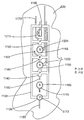
반도체 칩(1215)에 대한 또 다른 예시적인 실시예의 평면도가 도28에 도시된다. 반도체 칩(1215)의 오직 일부분만이 도시되어 있으며, 간략한 예시를 위해서 주변을 커버링하는 임의의 절연물질들은 도시되지 않았다. 예시적인 UBM 구조(1220)는 여러 개의 RDL 구조(1225, 1230, 1235, 1240, 1245) 위에 위치한 것으로 도시된다. UBM 구조(1220)에는 리드(lead) 구조의 여러 개의 클러스터(1250, 1255, 1260)들이 제공될 수 있다. 클러스터(1250)는 다수개의 리드들(leads)(1265, 1270, 1275, 1280, 1285, 1290, 1295, 1300)을 포함하는바, 이들 리드들은 각각의 스포크(spoke)(1310, 1315, 1320, 1325, 1330, 1335, 1340)에 의해서 중앙 허브(1305)에 연결된다. 상기 스포크는, 스포크(1310, 1320, 1330, 1340)들처럼 각각의 리드들에서 중단될 필요는 없다. 리드(1265)는 하부의 RDL 구조(1225)에 전기적으로 연결되며, 리드(1270, 1300)는 하부의 RDL 구조(1230)에 연결되며, 리드(1280, 1290)는 하부의 RDL 구조(1235)에 연결되며, 리드(1285)는 하부의 RDL 구조(1240)에 연결된다. 허브(1305)에는 접지 입력/출력으로 선정될 수 있는 솔더 범프(1350)가 제공될 수 있다. A top view of another exemplary embodiment of a
클러스터(1255)는 허브(1355)를 포함하며 또한, 각각의 스포크(1380, 1385, 1390, 1395)에 의해서 상기 허브로부터 연장되며 상기 허브에 연결되어 있는 다수개의 리드들(1360, 1365, 1370, 1375)을 포함한다. 리드(1360, 1365)는 하부의 RDL 구조(1245)에 연결되며, 리드(1370, 1375)는 하부의 RDL 구조(1235)에 연결된다. 클러스터(1255)는, 도시된 바와 같이 리드(1295)에서 혹은 소정의 다른 지점에서 클러스터(1250)에 결합될 수 있다. 솔더 볼(1397)이 상기 허브(1355)에 연결될 수 있다. The
마지막으로, 클러스터(1260)는 허브(1400), 스포크(1405, 1410, 1415, 1420, 1423), 그리도 상기 스포크(1405, 1410, 1415, 1420)에 각각 연결된 리드(1425, 1430, 1435, 1440)를 포함한다. 리드(1425, 1430)는 하부의 RDL 구조(1245)에 연결되며, 리드(1435, 1440)는 하부의 RDL 구조(1235)에 연결된다. 클러스터(1250) 및 클러스터(1255)와 유사하게, 클러스터(1260)에는 접지 입력/출력으로 선정될 수 있는 솔더 범프(1450)가 제공될 수 있다. 전원 범프(1460, 1465)는 하부의 RDL 구조(1470, 1475)에 연결된다. 도29를 참조하기 전에, 위치를 주목하라.Finally,
이제 도29를 참조하면, 도29에는 도28의 29-29 절단면이 도시되어 있다. 도29를 상세히 설명하기 전에 다음과 같이 점을 유의해야 한다. (1) 29-29 절단면은, 리드(1430), 허브(1400)와 솔더 볼(1450)의 결합, 리드(1440) 그리고 솔더 볼(1465)을 자르고 지나간다. (2) 도29는 도28에 도시되어 있지 않은 반도체 칩(1215)의 몇몇 세부 사항들을 도시하고 있는바, 따라서 다양한 전도체 구조 및 UBM 구조의 다른 세부사항들이 보여질 수 있다. 예컨대, 2개의 솔더 범프(1450, 1465)들은 측면적으로 분리되며 그리고 폴리이미드 혹은 다른 폴리머 물질 필름(1485)에 의해서 전기적으로 절연된다. 또한, 도28에서는 상기 필름(1485)이 도시되어 있지 않기 때문에 다른 구조물들이 잘 보였음을 다시 한번 상기해야 한다. 특히, 솔더 볼(1465) 아래에는 UBM 구조(1490)가 존재하는바, 상기 UBM 구조(1490)는 갭(1493)에 의해서 UBM 구조(1260)로부터 수평적으로 이격된다. 상기 갭(1493)은 절연 물질층(1495)의 일부인 절연 물질로 채워진다. 절연 물질층(1495)은 본 명세서에서 논의되었던 다른 실시예들에서 설명된 페시베이션층과 유사하게 구성될 수 있다. 앞서 언급한 바와 같이, 솔더 볼(1450)과 그 하부의 UBM 구조(이 경우에는 허브 1400) 사이에는 오믹 콘택이 확립된다. 상기 허브(1400)는 또한 리드 혹은 확장부(1503)에 의해서 그 하부의 RDL 구조(1500)(도28에는 미도시)와 오믹 콘택을 이룬다. 리드(1430, 1440)는 그 하부의 RDL 구조(1245, 1235)와 오믹 콘택을 이룬다. RDL 구조(1245, 1500, 1235)는 점선 박스 I, J, K 로 표시된 회로 구조들에 전기적으로 연결되는바, 상기 회로 구조들은 반도체 칩(1215)의 더 안쪽에 위치한다. 상기 회로 구조들 I, J, K는 도25의 회로 구조들 A, B, C, D 등등과 관련하여 논의된 것과 같은 유사한 유형이 될 수 있다. 솔더 범프(1465)는 그 하부의 UBM 구조(1490)와 오믹 콘택을 이루며, UBM 구조(1490)는 확장부 혹은 리드(1507)에 의해서 RDL 구조(1505)와 오믹 콘택을 이루는바, 상기 확장부 혹은 리드(1507)는 도28에 도시되어 있지 않다. RDL 구조(1505)는 점선 박스 L 로 표현된 하부의 회로 구조에 연결되며, 회로 구조 L은 회로 구조 I, J, K에 관하여 논의된 바와 같이 구성될 수 있다. Referring now to FIG. 29, FIG. 29 shows the 29-29 cut plane of FIG. Before describing FIG. 29 in detail, it should be noted that: (1) A cut surface 29-29 cuts through the
클러스터 구조는 전원(power), 접지(ground), 신호(signal)를 위해 이용될 수 있다. 전원, 접지 혹은 신호 입/출력을 위해 이용되는가에 관계없이, 클러스터 구조를 이용하는 것의 장점은 더 조밀한 배치 및 유연한 레이아웃이다. 해당 기술분야의 당업자라면, 주어진 클러스터에 대한 리드들 및 스포크의 개수는 변경될 수 있다는 점을 능히 이해할 것이다. 또한, 클러스터 구조는 본 명세서에 개시된 다른 유형의 UBM 구조와 함께 이용될 수도 있다. The cluster structure may be used for power, ground, and signal. Regardless of whether it is used for power, ground, or signal inputs / outputs, the advantages of using a cluster structure are more compact layout and flexible layout. Those skilled in the art will appreciate that the number of leads and spokes for a given cluster may vary. In addition, the cluster structure may be used with other types of UBM structures disclosed herein.
도30은 인쇄회로기판(1510)으로부터 위쪽으로 벗겨낸 반도체 칩(620)을 도시한 도면으로, 여기서 인쇄회로기판(1510)은 반도체 칩 패키지 기판 혹은 다른 유형의 인쇄회로기판이 될 수도 있다. 조립되는 경우, 반도체 칩(620)은 패키지 기판(1510)의 범프 어레이(1515) 상에 플립-칩 마운트된다. 범프 어레이(1515)는 위를 향하고 있으며 반도체 칩(620)의 솔더 범프(623, 625 등등)들과 결합하도록 설계된 다수개의 솔더 범프들을 포함하며, 이들 중 하나는 1520으로 표시된다. 기판(1510)은, 상기 기판(1510)에 연결될 몇몇 다른 전자 디바이스와의 입력/출력을 확립하기 위한 몇몇 유형의 상호연결 구조를 포함한다. 예시된 실시예에서, 다수개의 핀들(1525)로 구성된 핀 그리드 어레이가 기판(1510)으로부터 돌출되어 있다. 하지만, 볼 그리드 어레이, 랜드 그리드 어레이 혹은 다른 유형 상호연결들이 이용될 수도 있다. 소정의 핀(가령, 핀 1525)과 소정의 범프 위치(가령, 기판 1510 상의 범프 위치 1520) 사이에는, 전기적 상호연결 구조(점선 라인 1530으로 도시됨)에 의해서 전기적인 경로가 확립된다. 상호연결 구조(1530)는 하나 이상의 전도체 라인으로 구성될 수 있으며, 상기 전도체 라인은 기판(1510) 내의 서로 다른 평면(level) 상에 위치한 하나 이상의 상호연결들 상에 위치하거나 위치하지 않을 수도 있다. 30 illustrates a
다양한 이유들로 인해, 범프 어레이(1515)의 주변부(1535) 주위에 위치한 범프 위치들은 신호의 입/출력으로 전용되는 경향이 있으며, 그리고 범프 어레이(1515)의 코어 패드 위치(1540)는 전원 및 접지의 입/출력으로 전용되는 경향이 있다. 이와 같은 통상적인 설계 기법은 많은 설계 상황에서 만족스럽게 기능한다. 하지만, 소위 딥-범프(deep-bump)라는 소정의 설계 상황이 존재하는바, 딥-범프 상황에서는, 칩(620)의 에지(1550)에 상대적으로 가깝게 위치한 범프(가령, 반도체 칩 620의 범프 623)가 전원 혹은 접지 입/출력을 요구한다. 어레이(1515)의 주변부 범프 위치들(1535)은 신호의 입/출력으로 전용되는 경향이 있기 때문에, 소정의 핀(1525)으로부터 어레이(1515) 상의 주변부에 위치한 패드 사이트에 전원 혹은 접지를 라우팅시키기 위해서, 소정 종류의 매립형 상호연결 구조를 기판(1510) 내에 구현할 필요가 있을 수도 있다. 이러한 해결책은 비용이 많이 소비되며 또한, 기판 트레이스 라우팅(substrate trace routing)이 상당히 수정되어야만 한다면 성능 문제를 야기할 수도 있다. 하지만, 이러한 딥 범프(623)에 전원 혹은 접지 입/출력을 라우팅시키는데, 본 명세서에 개시된 UBM 라우팅이 이용될 수 있다. 이에 관하여, UBM 라우팅 구조(1555)는 딥 범프(623)와 칩(620)의 중앙에 위치한 범프들(1560) 중 하나에 전기적으로 연결된다. 범프들(623, 1560) 및 그 하부의 UBM 구조(1555) 사이에 절연 물질이 개재될 것이기 때문에, UBM 구조(1555)는 점선으로 도시되어 있다. UBM 구조(1555)는 본 명세서에 개시된 임의의 실시예들에서 논의된 바와 같이 구성될 수 있다. For various reasons, bump locations located around the
본 명세서에 개시된 예시적인 실시예들은 예컨대 반도체, 자기 디스크, 광 디스크 혹은 다른 저장매체와 같은 컴퓨터 판독가능 매체에 저장된 명령에서 구현될 수도 있으며 혹은 컴퓨터 데이터 신호로서 구현될 수도 있다. 명령들 혹은 소프트웨어는 본 명세서에 개시된 회로 구조들을 합성 및/또는 시뮬레이션할 수도 있다. 예시적인 실시예에서, Cadence APD 등등과 같은 전자 설계 자동화 프로그램(electronic design automation program)이, 회로 구조들을 합성하는데 이용될 수도 있다. 결과물인 코드가 회로 구조들을 제작하는데 이용될 수 있다. 본 발명의 다른 실시예에서, 고주파수 SPICE 시뮬레이터 등등과 같은 시뮬레이션 프로그램이 이용되어, 회로 구조들의 전기적 행동을 시뮬레이션할 수도 있다. Example embodiments disclosed herein may be implemented in instructions stored on a computer readable medium such as, for example, semiconductors, magnetic disks, optical disks or other storage media, or may be implemented as computer data signals. The instructions or software may synthesize and / or simulate the circuit structures disclosed herein. In an example embodiment, an electronic design automation program, such as Cadence APD or the like, may be used to synthesize the circuit structures. The resulting code can be used to fabricate circuit structures. In another embodiment of the present invention, a simulation program such as a high frequency SPICE simulator or the like may be used to simulate the electrical behavior of the circuit structures.
다양한 변형예들 및 대안적인 형태들이 본 발명에 적용가능하지만, 특정한 실시예들이 도면에서 일례로서 예시되었으며, 명세서에서 상세히 설명되었다. 하지만, 개시된 특정한 형태만으로 본 발명이 제한되는 것이 아님을 유의해야 한다. 이와 달리, 본 발명은 다음의 청구항들에서 정의된 바와 같은 본 발명의 사상 및 범위 내에 속하는 모든 수정예들, 변형예들 또는 등가물들을 커버한다는 점을 유의해야 한다. While various modifications and alternative forms are applicable to the present invention, certain embodiments have been illustrated by way of example in the drawings and are described in detail in the specification. It should be noted, however, that the invention is not limited to the specific forms disclosed. On the contrary, it should be noted that the present invention covers all modifications, variations or equivalents falling within the spirit and scope of the invention as defined in the following claims.
170 : 디바이스 180 : 일면
190 : 대향하는 일면 200 : 본드 패드
210 : 페이베이션층 225 : 개구부
230 : 금속화층 240 : 절연 필름170: device 180: one side
190: one side facing the surface 200: bond pad
210: passivation layer 225: opening
230: metallization layer 240: insulating film
Claims (27)
반도체 칩 상에 전도체 구조를 형성하는 단계, 상기 전도체 구조는 제 1 재분배층 구조(redistribution layer structure)에 전기적으로 연결된 제 1 사이트와 제 2 재분배층 구조에 전기적으로 연결된 제 2 사이트를 가지며; 그리고
상기 전도체 구조 상에 솔더 구조를 형성하는 단계
를 포함하는 제조 방법. As a manufacturing method,
Forming a conductor structure on the semiconductor chip, the conductor structure having a first site electrically connected to a first redistribution layer structure and a second site electrically connected to a second redistribution layer structure; And
Forming a solder structure on the conductor structure
≪ / RTI >
상기 제 1 사이트에 근접한(proximate) 상기 전도체 구조 상에 상기 솔더 구조를 형성하는 것을 특징으로 하는 제조 방법. The method of claim 1,
Forming the solder structure on the conductor structure proximate to the first site.
상기 제 2 사이트에 근접한 상기 전도체 구조 상에는 솔더 구조를 형성하지 않는 것을 특징으로 하는 제조 방법. The method of claim 1,
And a solder structure is not formed on the conductor structure proximate the second site.
상기 전도체 구조를 형성하는 단계는,
제 1 재분배층 구조에 전기적으로 결합된 제 1 사이트와 제 2 재분배층 구조에 전기적으로 결합된 제 2 사이트를 갖는 전도체 그리드를 형성하는 단계를 포함하는 것을 특징으로 하는 제조 방법. The method of claim 1,
Forming the conductor structure,
Forming a conductor grid having a first site electrically coupled to the first redistribution layer structure and a second site electrically coupled to the second redistribution layer structure.
상기 전도체 구조를 형성하는 단계는,
허브를 구비하고 적어도 상기 제 1 및 제 2 사이트가 상기 허브에 결합된 클러스터를 형성하는 단계를 포함하며, 상기 제 1 사이트는 상기 제 1 재분배층 구조에 연결되며 그리고 상기 제 2 사이트는 상기 제 2 재분배층 구조에 연결되는 것을 특징으로 하는 제조 방법. The method of claim 1,
Forming the conductor structure,
Forming a cluster having a hub, wherein at least the first and second sites are coupled to the hub, the first site being connected to the first redistribution layer structure and the second site being the second site; And a redistribution layer structure.
상기 반도체 칩을 기판에 결합시키고 그리고 상기 기판을 컴퓨팅 디바이스에 마운팅시키는 단계를 포함하는 제조 방법. 10. A method according to any one of the preceding claims,
Coupling the semiconductor chip to a substrate and mounting the substrate to a computing device.
상기 방법은 컴퓨터 판독가능 매체에 저장된 명령들을 실행함에 의해 수행되는 것을 특징으로 하는 제조 방법. 10. A method according to any one of the preceding claims,
And the method is performed by executing instructions stored on a computer readable medium.
반도체 칩 상에 제 1 전도체 구조를 형성하는 단계, 상기 제 1 전도체 구조는 제 1 재분배층 구조(redistribution layer structure)에 전기적으로 연결된 제 1 사이트와 제 2 재분배층 구조에 전기적으로 연결된 제 2 사이트를 가지며;
상기 반도체 칩 상에 제 2 전도체 구조를 형성하는 단계, 상기 제 2 전도체 구조는 제 3 재분배층 구조에 전기적으로 연결된 제 3 사이트와 제 4 재분배층 구조에 전기적으로 연결된 제 4 사이트를 가지며; 그리고
상기 제 1 전도체 구조 상에 제 1 솔더 구조를 형성하고 상기 제 2 전도체 구조 상에 제 2 솔더 구조를 형성하는 단계
를 포함하는 제조 방법. As a manufacturing method,
Forming a first conductor structure on the semiconductor chip, the first conductor structure comprising a first site electrically connected to the first redistribution layer structure and a second site electrically connected to the second redistribution layer structure Has;
Forming a second conductor structure on the semiconductor chip, the second conductor structure having a third site electrically connected to a third redistribution layer structure and a fourth site electrically connected to a fourth redistribution layer structure; And
Forming a first solder structure on the first conductor structure and forming a second solder structure on the second conductor structure
≪ / RTI >
상기 제 1 솔더 구조를 반도체 칩을 위한 접지 경로에 전기적으로 연결하는 단계와 상기 제 2 솔더 구조를 반도체 칩을 위한 전원 경로에 전기적으로 연결하는 단계를 포함하는 것을 특징으로 하는 제조 방법. The method of claim 8,
Electrically connecting the first solder structure to a ground path for a semiconductor chip and electrically connecting the second solder structure to a power path for a semiconductor chip.
상기 제 1 전도체 구조를 형성하는 단계는,
상기 제 1 재분배층 구조에 전기적으로 연결된 제 1 사이트와 상기 제 2 재분배층 구조에 전기적으로 연결된 제 2 사이트를 갖는 전도체 그리드(grid)를 형성하는 것을 특징으로 하는 제조 방법. The method of claim 8,
Forming the first conductor structure,
And forming a conductor grid having a first site electrically connected to the first redistribution layer structure and a second site electrically connected to the second redistribution layer structure.
상기 제 1 전도체 구조를 형성하는 단계는,
허브, 상기 허브에 결합된 적어도 상기 제 1 및 제 2 사이트, 상기 제 3 재분배층 구조에 연결된 상기 제 3 사이트, 그리고 상기 제 4 재분배층 구조에 연결된 상기 제 4 사이트를 갖는 클러스터를 형성하는 것을 특징으로 하는 제조 방법. The method according to any one of claims 8 to 10,
Forming the first conductor structure,
And forming a cluster having a hub, at least the first and second sites coupled to the hub, the third site connected to the third redistribution layer structure, and the fourth site connected to the fourth redistribution layer structure. Manufacturing method.
상기 제 1 사이트에 근접한 상기 제 1 전도체 구조 상에 상기 제 1 솔더 구조를 형성하는 것을 특징으로 하는 제조 방법. The method of claim 8,
Forming the first solder structure on the first conductor structure proximate the first site.
상기 제 1 사이트에 근접한 상기 제 1 전도체 구조 상에는 솔더 구조를 형성하지 않는 것을 특징으로 하는 제조 방법. The method of claim 8,
Wherein a solder structure is not formed on the first conductor structure proximate the first site.
상기 반도체 칩을 기판에 결합시키고 그리고 상기 기판을 컴퓨팅 디바이스에 마운팅시키는 단계를 포함하는 것을 특징으로 하는 제조 방법. The method according to any one of claims 8 to 13,
Coupling the semiconductor chip to a substrate and mounting the substrate to a computing device.
상기 방법은 컴퓨터 판독가능 매체에 저장된 명령들을 실행함에 의해서 수행되는 것을 특징으로 하는 제조 방법. The method according to any one of claims 8 to 14,
And the method is performed by executing instructions stored on a computer readable medium.
반도체 칩 상에 전도체 구조를 형성하는 단계, 상기 전도체 구조는 재분배층에 전기적으로 연결된 다수의 사이트들을 가지며; 그리고
상기 다수의 사이트들 중 하나에 근접한 상기 전도체 구조 상에 적어도 하나의 솔더 구조를 형성하는 단계
를 포함하는 제조 방법. As a manufacturing method,
Forming a conductor structure on the semiconductor chip, the conductor structure having a plurality of sites electrically connected to the redistribution layer; And
Forming at least one solder structure on the conductor structure proximate one of the plurality of sites
≪ / RTI >
상기 적어도 하나의 솔더 구조를 상기 반도체 칩을 위한 전원 경로에 전기적으로 연결하는 것을 포함하는 제조 방법. The method of claim 16,
Electrically connecting the at least one solder structure to a power path for the semiconductor chip.
상기 적어도 하나의 솔더 구조를 상기 반도체 칩을 위한 접지 경로에 전기적으로 연결하는 것을 포함하는 제조 방법. The method of claim 16,
Electrically connecting the at least one solder structure to a ground path for the semiconductor chip.
상기 다수의 전도체 패드들 중 나머지에 인접한 상기 전도체 구조 상에는 솔더 구조들을 형성하지 않는 것을 특징으로 하는 제조 방법. The method of claim 16,
Wherein no solder structures are formed on the conductor structure adjacent to the other of the plurality of conductor pads.
적어도 2개의 재분배층 구조들을 갖는 반도체 칩;
상기 반도체 칩 상의 전도체 구조, 상기 전도체 구조는 상기 적어도 2개의 재분배층 구조들 중 제 1 재분배층 구조에 전기적으로 연결된 제 1 사이트와 상기 적어도 2개의 재분배층 구조들 중 제 2 재분배층 구조에 전기적으로 연결된 제 2 사이트를 가지며; 그리고
상기 전도체 구조 상의 솔더 구조
를 포함하는 장치. As a device,
A semiconductor chip having at least two redistribution layer structures;
A conductor structure on the semiconductor chip, the conductor structure being electrically connected to a first site electrically connected to a first redistribution layer structure of the at least two redistribution layer structures and a second redistribution layer structure of the at least two redistribution layer structures Has a connected second site; And
Solder structure on the conductor structure
Device comprising a.
상기 적어도 2개의 재분배층 구조들은 동일 유형의 전기적 경로의 일부를 구성하는 것을 특징으로 하는 장치. The method of claim 20,
Wherein said at least two redistribution layer structures constitute part of an electrical path of the same type.
상기 전도체 구조는, 상기 적어도 2개의 재분배층 구조들 중 제 1 재분배층 구조에 결합된 제 1 사이트와 상기 적어도 2개의 재분배층 구조들 중 제 2 재분배층 구조에 결합된 제 2 사이트를 갖는 전도체 그리드를 포함하는 것을 특징으로 하는 장치. The method of claim 20,
The conductor structure includes a conductor grid having a first site coupled to a first redistribution layer structure of the at least two redistribution layer structures and a second site coupled to a second redistribution layer structure of the at least two redistribution layer structures. Apparatus comprising a.
상기 전도체 구조는, 허브 및 상기 허브에 결합된 제 1 및 제 2 사이트를 갖는 클러스터를 포함하는 것을 특징으로 하는 장치. The method of claim 20,
And wherein the conductor structure comprises a cluster having a hub and first and second sites coupled to the hub.
상기 솔더 구조는, 상기 제 1 사이트에 근접한 상기 전도체 구조 상에 위치하는 것을 특징으로 하는 장치. The method of claim 20,
The solder structure is located on the conductor structure proximate the first site.
상기 제 2 사이트에 근접한 상기 제 1 전도체 구조 상에는 솔더 구조가 존재하지 않는 것을 특징으로 하는 장치. The method of claim 20,
And wherein no solder structure is present on the first conductor structure proximate the second site.
상기 반도체 칩에 결합된 기판을 포함하는 것을 특징으로 하는 장치. The method according to any one of claims 20 to 25,
And a substrate coupled to the semiconductor chip.
상기 기판에 결합된 컴퓨팅 디바이스를 포함하는 것을 특징으로 하는 장치. The method of claim 26,
And a computing device coupled to the substrate.
Applications Claiming Priority (2)
| Application Number | Priority Date | Filing Date | Title |
|---|---|---|---|
| US11/949,951 US20090032941A1 (en) | 2007-08-01 | 2007-12-04 | Under Bump Routing Layer Method and Apparatus |
| US11/949,951 | 2007-12-04 |
Publications (1)
| Publication Number | Publication Date |
|---|---|
| KR20100102635A true KR20100102635A (en) | 2010-09-24 |
Family
ID=40592064
Family Applications (1)
| Application Number | Title | Priority Date | Filing Date |
|---|---|---|---|
| KR1020107014910A KR20100102635A (en) | 2007-12-04 | 2008-12-04 | Under bump routing layer method and apparatus |
Country Status (6)
| Country | Link |
|---|---|
| US (1) | US20090032941A1 (en) |
| EP (1) | EP2229694B1 (en) |
| JP (2) | JP5567489B2 (en) |
| KR (1) | KR20100102635A (en) |
| CN (1) | CN101952962A (en) |
| WO (1) | WO2009071982A2 (en) |
Families Citing this family (16)
| Publication number | Priority date | Publication date | Assignee | Title |
|---|---|---|---|---|
| US7790501B2 (en) * | 2008-07-02 | 2010-09-07 | Ati Technologies Ulc | Semiconductor chip passivation structures and methods of making the same |
| US8278748B2 (en) * | 2010-02-17 | 2012-10-02 | Maxim Integrated Products, Inc. | Wafer-level packaged device having self-assembled resilient leads |
| TWI541964B (en) * | 2010-11-23 | 2016-07-11 | 矽品精密工業股份有限公司 | Fabrication method of semiconductor substrate |
| US20120175772A1 (en) * | 2011-01-07 | 2012-07-12 | Leung Andrew K | Alternative surface finishes for flip-chip ball grid arrays |
| US8647974B2 (en) | 2011-03-25 | 2014-02-11 | Ati Technologies Ulc | Method of fabricating a semiconductor chip with supportive terminal pad |
| US8564030B2 (en) | 2011-06-10 | 2013-10-22 | Advanced Micro Devices | Self-aligned trench contact and local interconnect with replacement gate process |
| US8716124B2 (en) | 2011-11-14 | 2014-05-06 | Advanced Micro Devices | Trench silicide and gate open with local interconnect with replacement gate process |
| WO2013101243A1 (en) | 2011-12-31 | 2013-07-04 | Intel Corporation | High density package interconnects |
| US9257276B2 (en) * | 2011-12-31 | 2016-02-09 | Intel Corporation | Organic thin film passivation of metal interconnections |
| TWI585946B (en) * | 2012-11-30 | 2017-06-01 | 英力股份有限公司 | Semiconductor device and method of forming the same |
| CN103887248B (en) * | 2012-12-21 | 2017-12-12 | 比亚迪股份有限公司 | A kind of IGBT structure and preparation method thereof |
| GB2520952A (en) | 2013-12-04 | 2015-06-10 | Ibm | Flip-chip electronic device with carrier having heat dissipation elements free of solder mask |
| JP6771308B2 (en) * | 2016-05-02 | 2020-10-21 | 三菱電機株式会社 | Mounting structure of circuit boards and semiconductor integrated circuits |
| DE102018105166B4 (en) * | 2017-11-15 | 2024-01-18 | Taiwan Semiconductor Manufacturing Co., Ltd. | TWO DEVICES FOR A SEMICONDUCTOR PACKAGE AND METHOD FOR PRODUCING A SEMICONDUCTOR PACKAGE |
| WO2019116482A1 (en) * | 2017-12-14 | 2019-06-20 | 三菱電機株式会社 | Semiconductor device |
| CN114695224A (en) * | 2020-12-29 | 2022-07-01 | 联华电子股份有限公司 | Chip bonding alignment structure, bonded chip structure and manufacturing method thereof |
Family Cites Families (47)
| Publication number | Priority date | Publication date | Assignee | Title |
|---|---|---|---|---|
| US3593319A (en) * | 1968-12-23 | 1971-07-13 | Gen Electric | Card-changeable capacitor read-only memory |
| US4249196A (en) * | 1978-08-21 | 1981-02-03 | Burroughs Corporation | Integrated circuit module with integral capacitor |
| JPS56101732A (en) * | 1980-01-18 | 1981-08-14 | Matsushita Electric Ind Co Ltd | Metallized film condenser |
| US4409608A (en) * | 1981-04-28 | 1983-10-11 | The United States Of America As Represented By The Secretary Of The Navy | Recessed interdigitated integrated capacitor |
| GB2115223B (en) * | 1982-02-18 | 1985-07-10 | Standard Telephones Cables Ltd | Multilayer ceramic dielectric capacitors |
| US4901128A (en) * | 1982-11-04 | 1990-02-13 | Hitachi, Ltd. | Semiconductor memory |
| KR900001394B1 (en) * | 1985-04-05 | 1990-03-09 | Fujitsu Ltd | Super high frequency intergrated circuit device |
| US4685197A (en) * | 1986-01-07 | 1987-08-11 | Texas Instruments Incorporated | Fabricating a stacked capacitor |
| EP0246808B1 (en) * | 1986-05-16 | 1993-01-20 | Showa Denko Kabushiki Kaisha | Solid electrolytic capacitor |
| JPS6370550A (en) * | 1986-09-12 | 1988-03-30 | Nec Corp | Semiconductor integrated circuit |
| JPH01209746A (en) * | 1988-02-17 | 1989-08-23 | Nec Corp | Semiconductor device |
| US4866567A (en) * | 1989-01-06 | 1989-09-12 | Ncr Corporation | High frequency integrated circuit channel capacitor |
| US4914546A (en) * | 1989-02-03 | 1990-04-03 | Micrel Incorporated | Stacked multi-polysilicon layer capacitor |
| US5053916A (en) * | 1989-03-13 | 1991-10-01 | U.S. Philips Corporation | Surface-mounted multilayer capacitor and printed circuit board having such a multilayer capacitor |
| US5089878A (en) * | 1989-06-09 | 1992-02-18 | Lee Jaesup N | Low impedance packaging |
| US5081559A (en) * | 1991-02-28 | 1992-01-14 | Micron Technology, Inc. | Enclosed ferroelectric stacked capacitor |
| US5189594A (en) * | 1991-09-20 | 1993-02-23 | Rohm Co., Ltd. | Capacitor in a semiconductor integrated circuit and non-volatile memory using same |
| US5155658A (en) * | 1992-03-05 | 1992-10-13 | Bell Communications Research, Inc. | Crystallographically aligned ferroelectric films usable in memories and method of crystallographically aligning perovskite films |
| US5208725A (en) * | 1992-08-19 | 1993-05-04 | Akcasu Osman E | High capacitance structure in a semiconductor device |
| JP3057130B2 (en) * | 1993-02-18 | 2000-06-26 | 三菱電機株式会社 | Resin-sealed semiconductor package and method of manufacturing the same |
| JP3160198B2 (en) * | 1995-02-08 | 2001-04-23 | インターナショナル・ビジネス・マシーンズ・コーポレ−ション | Semiconductor substrate on which decoupling capacitor is formed and method of manufacturing the same |
| US5874782A (en) * | 1995-08-24 | 1999-02-23 | International Business Machines Corporation | Wafer with elevated contact structures |
| JP3147162B2 (en) * | 1998-07-13 | 2001-03-19 | 日本電気株式会社 | Bump arrangement method for flip chip integrated circuit and flip chip integrated circuit |
| JP3530761B2 (en) * | 1999-01-18 | 2004-05-24 | 新光電気工業株式会社 | Semiconductor device |
| US6656828B1 (en) * | 1999-01-22 | 2003-12-02 | Hitachi, Ltd. | Method of forming bump electrodes |
| JP4004196B2 (en) * | 1999-11-16 | 2007-11-07 | イビデン株式会社 | Semiconductor chip |
| JP2001168125A (en) * | 1999-12-03 | 2001-06-22 | Nec Corp | Semiconductor device |
| US6387795B1 (en) * | 2001-03-22 | 2002-05-14 | Apack Technologies Inc. | Wafer-level packaging |
| US7215022B2 (en) * | 2001-06-21 | 2007-05-08 | Ati Technologies Inc. | Multi-die module |
| WO2003012863A1 (en) * | 2001-07-31 | 2003-02-13 | Renesas Technology Corp. | Semiconductor device and its manufacturing method |
| US6979896B2 (en) * | 2001-10-30 | 2005-12-27 | Intel Corporation | Power gridding scheme |
| JP3768433B2 (en) * | 2001-11-19 | 2006-04-19 | 株式会社ルネサステクノロジ | Semiconductor device design method |
| DE10159466A1 (en) * | 2001-12-04 | 2003-06-12 | Koninkl Philips Electronics Nv | Arrangement with capacitor |
| JP2004079801A (en) * | 2002-08-19 | 2004-03-11 | Fujitsu Ltd | Capacitor device and its manufacturing method |
| US7112884B2 (en) * | 2002-08-23 | 2006-09-26 | Ati Technologies, Inc. | Integrated circuit having memory disposed thereon and method of making thereof |
| US6861749B2 (en) * | 2002-09-20 | 2005-03-01 | Himax Technologies, Inc. | Semiconductor device with bump electrodes |
| US7161793B2 (en) * | 2002-11-14 | 2007-01-09 | Fujitsu Limited | Layer capacitor element and production process as well as electronic device |
| JP4571781B2 (en) * | 2003-03-26 | 2010-10-27 | ルネサスエレクトロニクス株式会社 | Semiconductor device and manufacturing method thereof |
| US7180195B2 (en) * | 2003-12-17 | 2007-02-20 | Intel Corporation | Method and apparatus for improved power routing |
| JP4904670B2 (en) * | 2004-06-02 | 2012-03-28 | 富士通セミコンダクター株式会社 | Semiconductor device |
| TWI299248B (en) * | 2004-09-09 | 2008-07-21 | Phoenix Prec Technology Corp | Method for fabricating conductive bumps of a circuit board |
| JP4449824B2 (en) * | 2005-06-01 | 2010-04-14 | カシオ計算機株式会社 | Semiconductor device and its mounting structure |
| US7473999B2 (en) * | 2005-09-23 | 2009-01-06 | Megica Corporation | Semiconductor chip and process for forming the same |
| JP4595823B2 (en) * | 2006-01-24 | 2010-12-08 | 株式会社デンソー | Ball grid array |
| US20070176292A1 (en) * | 2006-01-27 | 2007-08-02 | Taiwan Semiconductor Manufacturing Co., Ltd. | Bonding pad structure |
| JP5157191B2 (en) * | 2006-03-01 | 2013-03-06 | 日立化成株式会社 | Semiconductor device |
| JP2006203261A (en) * | 2006-04-26 | 2006-08-03 | Renesas Technology Corp | Semiconductor apparatus |
-
2007
- 2007-12-04 US US11/949,951 patent/US20090032941A1/en not_active Abandoned
-
2008
- 2008-12-04 CN CN2008801260899A patent/CN101952962A/en active Pending
- 2008-12-04 KR KR1020107014910A patent/KR20100102635A/en not_active Application Discontinuation
- 2008-12-04 EP EP08855955.4A patent/EP2229694B1/en active Active
- 2008-12-04 JP JP2010536543A patent/JP5567489B2/en not_active Expired - Fee Related
- 2008-12-04 WO PCT/IB2008/003343 patent/WO2009071982A2/en active Application Filing
-
2013
- 2013-02-19 JP JP2013030065A patent/JP5654067B2/en not_active Expired - Fee Related
Also Published As
| Publication number | Publication date |
|---|---|
| JP2011505705A (en) | 2011-02-24 |
| WO2009071982A3 (en) | 2009-07-23 |
| JP5654067B2 (en) | 2015-01-14 |
| JP2013093630A (en) | 2013-05-16 |
| US20090032941A1 (en) | 2009-02-05 |
| JP5567489B2 (en) | 2014-08-06 |
| EP2229694A2 (en) | 2010-09-22 |
| WO2009071982A2 (en) | 2009-06-11 |
| CN101952962A (en) | 2011-01-19 |
| EP2229694B1 (en) | 2017-01-25 |
Similar Documents
| Publication | Publication Date | Title |
|---|---|---|
| JP5654067B2 (en) | Method and apparatus for under bump wiring layer | |
| US12094853B2 (en) | Semiconductor chip with redundant thru-silicon-vias | |
| KR100772604B1 (en) | Integrated Electronic Chip and Interconnect Device and Process for Making the Same | |
| US7969020B2 (en) | Die stacking apparatus and method | |
| TWI394218B (en) | Highly reliable low-cost structure for wafer-level ball grid array packaging | |
| US20170250153A1 (en) | Electronic part, electronic device, and electronic apparatus | |
| KR101508669B1 (en) | Semiconductor chip with supportive terminal pad | |
| US8153516B2 (en) | Method of ball grid array package construction with raised solder ball pads | |
| TW201911508A (en) | Electronic package | |
| US20120326299A1 (en) | Semiconductor chip with dual polymer film interconnect structures | |
| US20130256871A1 (en) | Semiconductor chip device with fragmented solder structure pads | |
| US8294266B2 (en) | Conductor bump method and apparatus | |
| JP2013110375A (en) | Semiconductor package and semiconductor package module including the same | |
| KR102633431B1 (en) | Semiconductor device and manufacturing method thereof | |
| US20130256895A1 (en) | Stacked semiconductor components with universal interconnect footprint | |
| JP2007103855A (en) | Substrate for semiconductor device and semiconductor device | |
| JP3726906B2 (en) | Semiconductor device and manufacturing method thereof, circuit board, and electronic apparatus | |
| CN116741715A (en) | Semiconductor device and method of forming the same | |
| KR20190136240A (en) | Package board and method of manufacturing the same | |
| JP2005026299A (en) | Semiconductor device, its manufacturing method, circuit board, and electronic apparatus |
Legal Events
| Date | Code | Title | Description |
|---|---|---|---|
| A201 | Request for examination | ||
| E902 | Notification of reason for refusal | ||
| E601 | Decision to refuse application |