KR20100086432A - Rfid tag - Google Patents
Rfid tag Download PDFInfo
- Publication number
- KR20100086432A KR20100086432A KR1020100005466A KR20100005466A KR20100086432A KR 20100086432 A KR20100086432 A KR 20100086432A KR 1020100005466 A KR1020100005466 A KR 1020100005466A KR 20100005466 A KR20100005466 A KR 20100005466A KR 20100086432 A KR20100086432 A KR 20100086432A
- Authority
- KR
- South Korea
- Prior art keywords
- transistor
- output
- inverter
- analog switch
- turned
- Prior art date
Links
Images


Classifications
-
- G—PHYSICS
- G06—COMPUTING; CALCULATING OR COUNTING
- G06K—GRAPHICAL DATA READING; PRESENTATION OF DATA; RECORD CARRIERS; HANDLING RECORD CARRIERS
- G06K19/00—Record carriers for use with machines and with at least a part designed to carry digital markings
- G06K19/06—Record carriers for use with machines and with at least a part designed to carry digital markings characterised by the kind of the digital marking, e.g. shape, nature, code
- G06K19/067—Record carriers with conductive marks, printed circuits or semiconductor circuit elements, e.g. credit or identity cards also with resonating or responding marks without active components
- G06K19/07—Record carriers with conductive marks, printed circuits or semiconductor circuit elements, e.g. credit or identity cards also with resonating or responding marks without active components with integrated circuit chips
- G06K19/073—Special arrangements for circuits, e.g. for protecting identification code in memory
-
- G—PHYSICS
- G11—INFORMATION STORAGE
- G11C—STATIC STORES
- G11C11/00—Digital stores characterised by the use of particular electric or magnetic storage elements; Storage elements therefor
- G11C11/21—Digital stores characterised by the use of particular electric or magnetic storage elements; Storage elements therefor using electric elements
- G11C11/34—Digital stores characterised by the use of particular electric or magnetic storage elements; Storage elements therefor using electric elements using semiconductor devices
- G11C11/40—Digital stores characterised by the use of particular electric or magnetic storage elements; Storage elements therefor using electric elements using semiconductor devices using transistors
- G11C11/41—Digital stores characterised by the use of particular electric or magnetic storage elements; Storage elements therefor using electric elements using semiconductor devices using transistors forming static cells with positive feedback, i.e. cells not needing refreshing or charge regeneration, e.g. bistable multivibrator or Schmitt trigger
- G11C11/412—Digital stores characterised by the use of particular electric or magnetic storage elements; Storage elements therefor using electric elements using semiconductor devices using transistors forming static cells with positive feedback, i.e. cells not needing refreshing or charge regeneration, e.g. bistable multivibrator or Schmitt trigger using field-effect transistors only
-
- H—ELECTRICITY
- H03—ELECTRONIC CIRCUITRY
- H03K—PULSE TECHNIQUE
- H03K17/00—Electronic switching or gating, i.e. not by contact-making and –breaking
- H03K17/30—Modifications for providing a predetermined threshold before switching
- H03K17/302—Modifications for providing a predetermined threshold before switching in field-effect transistor switches
-
- H—ELECTRICITY
- H03—ELECTRONIC CIRCUITRY
- H03K—PULSE TECHNIQUE
- H03K19/00—Logic circuits, i.e. having at least two inputs acting on one output; Inverting circuits
-
- H—ELECTRICITY
- H01—ELECTRIC ELEMENTS
- H01L—SEMICONDUCTOR DEVICES NOT COVERED BY CLASS H10
- H01L2924/00—Indexing scheme for arrangements or methods for connecting or disconnecting semiconductor or solid-state bodies as covered by H01L24/00
- H01L2924/0001—Technical content checked by a classifier
- H01L2924/0002—Not covered by any one of groups H01L24/00, H01L24/00 and H01L2224/00
Abstract
Description
본 발명은 반도체 장치에 관한 것이다. 또는 본 발명은 RFID(Radio Frequency Identification) 기술을 이용한 무선 태그(RFID 태그, IC 태그, ID 태그라고도 함)에 관한 것이다. The present invention relates to a semiconductor device. Alternatively, the present invention relates to a radio tag (also called an RFID tag, an IC tag, and an ID tag) using a radio frequency identification (RFID) technology.
무선 통신에 의해 데이터를 교신할 수 있는 자동 인식 기술로서, RFID가 널리 퍼져 있다. RFID는, 정보를 기억 가능한 RFID 태그와, RFID 태그에 기억된 정보의 판독이나 RFID 태그로 정보의 기록을 행하는 리더/라이터로 이루어진다. RFID 태그는 예를 들어 안테나 등을 가지는 반도체 장치로 이루어진다. RFID is widely used as an automatic recognition technology that can communicate data by wireless communication. The RFID includes an RFID tag capable of storing information and a reader / writer for reading the information stored in the RFID tag and recording the information with the RFID tag. The RFID tag is made of, for example, a semiconductor device having an antenna or the like.
RFID 태그는 세션 플래그를 구비하고 있다(특허문헌 1). 세션 플래그는, RFID 태그로부터 정보를 판독한 후에, 재차 판독하는 것을 방지한다. 세션 플래그는, 예를 들어, "A" 및 "B"의 2개의 상태를 가지고, 정보를 판독하였을 때에 "A"로부터 "B"로 설정된다. The RFID tag has a session flag (Patent Document 1). The session flag prevents reading again after reading the information from the RFID tag. The session flag has two states, for example, "A" and "B", and is set from "A" to "B" when information is read.
정보가 판독되고, 세션 플래그가 "A"로부터 "B"로 된 후, 전파가 일시적으로 도중에 끊어져도, RFID 태그에 형성된 메모리가 세션 플래그의 상태를 보유하고 있다. 다시 RFID 태그가 전파를 수신하여도, 세션 플래그가 상태"B"로 되어 있기 때문에, RFID 태그는 "판독 완료"의 스테이터스가 되어 있고, 한번 정보를 판독한 RFID 태그의 재판독을 방지할 수 있다. After the information is read and the session flag is changed from "A" to "B", even if the radio wave is temporarily interrupted, the memory formed in the RFID tag retains the state of the session flag. Even if the RFID tag receives radio waves again, since the session flag is in the state "B", the RFID tag has a status of "reading completion" and can prevent rereading of the RFID tag once the information has been read. .
통상, 메모리는 트랜지스터 및 용량을 가지고, 용량에 전하를 축적하여 정보를 기억하고 있다. 그러나 용량에 축적된 전하는 여러 가지 요인에 의해 누설된다. 누설 전류의 주된 원인은 트랜지스터로부터의 누설 전류를 들 수 있다. 이 때문에 리플레쉬가 필요하게 된다. 또 리플레쉬란, 전하가 완전히 소실되기 전에, 메모리에 축적되어 있는 정보를 판독하고, 그 판독 정보를 바탕으로 하여, 다시 메모리로 전하를 축적함으로써 정보의 기록을 행하는 동작이다. In general, a memory has a transistor and a capacitor, and charges are stored in the capacitor to store information. However, the charge accumulated in the capacity is leaked by various factors. The main cause of the leakage current is the leakage current from the transistor. This requires refreshing. The refresh is an operation in which information stored in the memory is read before the charge is completely lost, and the information is written by accumulating the charge in the memory again based on the read information.
본 발명의 일 형태의 과제는, 트랜지스터와 용량에 의해서 정보를 기억하고, 리플레쉬를 필요로 하지 않는 RFID 태그를 제공한다. An object of one embodiment of the present invention is to provide an RFID tag which stores information by a transistor and a capacity and does not require refreshing.
본 발명의 일 형태는, 트랜지스터와, 트랜지스터의 소스 및 드레인의 한쪽에 접속된 용량을 가지고, 용량에 축적된 전하에 대응하는 전압을 트랜지스터의 소스 및 드레인의 다른쪽에 인가하는 RFID 태그이다. 축적된 전하는 트랜지스터의 소스 및 드레인의 다른쪽으로 누설되지 않고, 용량에 보유된다. One embodiment of the present invention is an RFID tag having a transistor and a capacitor connected to one of a source and a drain of the transistor, and applying a voltage corresponding to the charge accumulated in the capacitor to the other of the source and the drain of the transistor. The accumulated charge does not leak to the other side of the source and drain of the transistor, but is retained in the capacitance.
본 발명의 일 형태는, 제 1 트랜지스터, 제 2 트랜지스터, 제 3 트랜지스터, 용량 및 버퍼를 가지고, 제 2 트랜지스터의 소스 및 드레인의 한쪽은 입력 단자에 전기적으로 접속되고, 소스 및 드레인의 다른쪽은, 제 1 트랜지스터의 소스 및 드레인의 한쪽 또는 제 3 트랜지스터의 소스 및 드레인의 한쪽에 전기적으로 접속되고, 제 1 트랜지스터의 소스 및 드레인의 다른쪽은 용량의 한쪽의 전극 또한 버퍼의 입력에 전기적으로 접속되고, 용량의 다른쪽의 전극은 기준 전압 단자에 전기적으로 접속되고, 버퍼의 출력은 출력 단자 및 제 3 트랜지스터의 소스 및 드레인의 다른쪽에 전기적으로 접속되는 RFID 태그이다. One embodiment of the present invention has a first transistor, a second transistor, a third transistor, a capacitor, and a buffer, one of the source and the drain of the second transistor is electrically connected to an input terminal, and the other of the source and the drain is One of the source and the drain of the first transistor or one of the source and the drain of the third transistor, the other of the source and the drain of the first transistor is electrically connected to one electrode of the capacitor and also to the input of the buffer And the other electrode of the capacitor is electrically connected to the reference voltage terminal, and the output of the buffer is an RFID tag that is electrically connected to the other of the source and the drain of the output terminal and the third transistor.
제 2 트랜지스터 및 제 1 트랜지스터가 온으로 되고, 입력 단자로부터 용량에 전하가 축적되고, 전하에 대응한 정보가 버퍼로부터 출력 단자에 출력되고, 전하가 축적된 후, 제 2 트랜지스터 및 제 1 트랜지스터가 오프로 되는 동시에 제 3 트랜지스터가 온으로 되고, 버퍼로부터의 출력이 제 1 트랜지스터의 소스 및 드레인의 한쪽에 인가되고, 용량에 축적된 전하는 제 1 트랜지스터의 소스 및 드레인의 한쪽으로 누설되지 않고, 용량에 보유된다. After the second transistor and the first transistor are turned on, charge is accumulated in the capacitance from the input terminal, information corresponding to the charge is output from the buffer to the output terminal, and after the charge is accumulated, the second transistor and the first transistor are The third transistor is turned on and the output from the buffer is applied to one of the source and the drain of the first transistor, and the charge accumulated in the capacitance does not leak to one of the source and the drain of the first transistor, Is held in.
제 2 트랜지스터 및 제 1 트랜지스터가 온으로 되고, 용량에 축적된 전하가 제 1 트랜지스터의 소스 및 드레인의 한쪽으로 방출되고, 전하의 방출에 대응한 정보가 버퍼로부터 출력 단자에 출력되고, 전하가 방출된 후, 제 2 트랜지스터 및 제 1 트랜지스터가 오프로 되는 동시에 제 3 트랜지스터가 온으로 되고, 버퍼로부터의 출력이 제 1 트랜지스터의 소스 및 드레인의 한쪽에 인가된다. The second transistor and the first transistor are turned on, the charge accumulated in the capacitor is discharged to one of the source and the drain of the first transistor, information corresponding to the discharge of the charge is output from the buffer to the output terminal, and the charge is discharged. After that, the second transistor and the first transistor are turned off and at the same time the third transistor is turned on, and the output from the buffer is applied to one of the source and the drain of the first transistor.
본 발명의 일 형태는, 제 1 인버터, 제 2 인버터, 제 1 트랜지스터, 용량, 버퍼, 제 1 아날로그 스위치, 제 2 아날로그 스위치, 제 1 입력 단자, 제 2 입력 단자 및 출력 단자를 가지고, 제 1 입력 단자는 제 1 인버터의 입력에 전기적으로 접속되고, 제 1 인버터의 출력은 제 2 인버터의 입력, 제 1 아날로그 스위치의 제 2 제어 단자 및 제 2 아날로그 스위치의 제 1 제어 단자에 전기적으로 접속되고, 제 2 인버터의 출력은 제 1 아날로그 스위치의 제 1 제어 단자, 제 2 아날로그 스위치의 제 2 제어 단자 및 제 1 트랜지스터의 게이트에 전기적으로 접속되고, 제 2 입력단자는 제 1 아날로그 스위치의 입력에 전기적으로 접속되고, 제 1 아날로그 스위치의 출력은 제 1 트랜지스터의 소스 및 드레인의 한쪽 또는 제 2 아날로그 스위치의 출력에 전기적으로 접속되고, 제 1 트랜지스터의 소스 및 드레인의 다른쪽은 용량의 한쪽의 전극 및 버퍼의 입력에 전기적으로 접속되고, 용량의 다른쪽의 전극은 기준 전압 단자에 전기적으로 접속되고, 버퍼의 출력은 출력 단자 및 제 2 아날로그 스위치의 입력에 전기적으로 접속되는 RFID 태그이다. One embodiment of the present invention has a first inverter, a second inverter, a first transistor, a capacitor, a buffer, a first analog switch, a second analog switch, a first input terminal, a second input terminal, and an output terminal. The input terminal is electrically connected to the input of the first inverter, the output of the first inverter is electrically connected to the input of the second inverter, the second control terminal of the first analog switch and the first control terminal of the second analog switch, The output of the second inverter is electrically connected to the first control terminal of the first analog switch, the second control terminal of the second analog switch and the gate of the first transistor, and the second input terminal is connected to the input of the first analog switch. Electrically connected, the output of the first analog switch is electrically connected to the output of one or the second analog switch of the source and the drain of the first transistor, The other of the source and drain of the transistor is electrically connected to one electrode of the capacitor and the input of the buffer, the other electrode of the capacitor is electrically connected to the reference voltage terminal, and the output of the buffer is connected to the output terminal and the second. An RFID tag that is electrically connected to the input of an analog switch.
제 1 입력 단자로부터 제 1 인버터에 신호가 입력됨으로써 얻어지는 제 1 인버터 및 제 2 인버터로부터의 출력에 의해, 제 1 아날로그 스위치 및 제 1 트랜지스터가 온으로 되는 동시에 제 2 아날로그 스위치가 오프로 되고, 제 2 입력 단자로부터 용량에 전하가 축적되고, 전하에 대응한 정보가 버퍼로부터 출력 단자에 출력되고, 전하가 축적된 후, 제 1 입력 단자로부터 제 1 인버터에 신호가 입력됨으로써 얻어지는 제 1 인버터 및 제 2 인버터로부터의 출력에 의해, 제 1 아날로그 스위치 및 제 1 트랜지스터가 오프로 되는 동시에 제 2 아날로그 스위치가 온으로 되고, 버퍼로부터의 출력이 제 1 트랜지스터의 소스 및 드레인의 한쪽에 인가되고, 용량에 축적된 전하는 제 1 트랜지스터의 소스 및 드레인의 한쪽으로 누설되지 않고, 용량에 보유된다. By the output from the 1st inverter and the 2nd inverter obtained by inputting a signal to a 1st inverter from a 1st input terminal, a 1st analog switch and a 1st transistor are turned on and a 2nd analog switch is turned off, The first inverter and the first obtained by accumulating charge in the capacitance from the two input terminals, outputting information corresponding to the charge from the buffer to the output terminal, and inputting signals to the first inverter from the first input terminal after the charge is accumulated. By the output from the two inverters, the first analog switch and the first transistor are turned off and the second analog switch is turned on, and the output from the buffer is applied to one of the source and the drain of the first transistor, The accumulated charge does not leak to either of the source and the drain of the first transistor, but is retained in the capacitance.
제 1 입력 단자로부터 제 1 인버터에 신호가 입력됨으로써 얻어지는 제 1 인버터 및 제 2 인버터로부터의 출력에 의해, 제 1 아날로그 스위치 및 제 1 트랜지스터가 온으로 되는 동시에 제 2 아날로그 스위치가 오프로 되고, 용량에 축적된 전하가 제 1 트랜지스터의 소스 및 드레인의 한쪽으로 방출되고, 전하의 방출에 대응한 정보가 버퍼로부터 출력 단자에 출력되고, 전하가 방출된 후, 제 1 입력 단자로부터 제 1 인버터에 신호가 입력됨으로써 얻어지는 제 1 인버터 및 제 2 인버터로부터의 출력에 의해, 제 1 아날로그 스위치 및 제 1 트랜지스터가 오프로 되는 동시에 제 2 아날로그 스위치가 온으로 되고, 버퍼로부터의 출력이 제 1 트랜지스터의 소스 및 드레인의 한쪽에 인가된다. By the output from the 1st inverter and the 2nd inverter obtained by inputting a signal to a 1st inverter from a 1st input terminal, a 1st analog switch and a 1st transistor are turned on and a 2nd analog switch is turned off and a capacitance Charge accumulated in the first transistor is discharged to one of the source and the drain of the first transistor, information corresponding to the discharge of the charge is output from the buffer to the output terminal, and after the charge is released, the signal is transmitted from the first input terminal to the first inverter. The first analog switch and the first transistor are turned off and the second analog switch is turned on by the outputs from the first inverter and the second inverter obtained by inputting the output of the first transistor. It is applied to one side of the drain.
본 발명의 일 형태는, 안테나, 정류 회로, 로직부 및 플래그 보유 회로를 가지고, 안테나는 정류 회로에 접속되고, 정류 회로는 로직부 및 플래그 보유 회로에 접속되고, 로직부는 클록 회로, 논리 회로, 복조 회로 및 변조 회로를 가지고, 플래그 보유 회로는, 제 1 트랜지스터, 제 2 트랜지스터, 제 3 트랜지스터, 용량 및 버퍼를 가지고, 제 2 트랜지스터의 게이트는 논리 회로에 전기적으로 접속되고, 소스 및 드레인의 한쪽은 입력 단자에 전기적으로 접속되고, 소스 및 드레인의 다른쪽은, 제 1 트랜지스터의 소스 및 드레인의 한쪽 또는 제 3 트랜지스터의 소스 및 드레인의 한쪽에 전기적으로 접속되고, 제 1 트랜지스터의 게이트는 논리 회로에 전기적으로 접속되고, 소스 및 드레인의 다른쪽은 용량의 한쪽의 전극 또한 버퍼의 입력에 전기적으로 접속되고, 용량의 다른쪽의 전극은 기준 전압 단자에 전기적으로 접속되고, 버퍼의 출력은 출력 단자 및 제 3 트랜지스터의 소스 및 드레인의 다른쪽에 전기적으로 접속되고, 제 3 트랜지스터의 게이트는 논리 회로에 전기적으로 접속되는 RFID 태그이다. One embodiment of the present invention has an antenna, a rectifying circuit, a logic section and a flag holding circuit, the antenna is connected to a rectifying circuit, the rectifying circuit is connected to a logic section and a flag holding circuit, the logic section is a clock circuit, a logic circuit, Has a demodulation circuit and a modulation circuit, the flag holding circuit has a first transistor, a second transistor, a third transistor, a capacitor and a buffer, the gate of the second transistor is electrically connected to the logic circuit, and one of the source and the drain Is electrically connected to an input terminal, the other of the source and the drain is electrically connected to one of the source and the drain of the first transistor or the one of the source and the drain of the third transistor, and the gate of the first transistor is a logic circuit. The other of the source and the drain is electrically connected to one electrode of the capacitor and also to the input of the buffer. The other electrode of the capacitor is electrically connected to the reference voltage terminal, the output of the buffer is electrically connected to the output terminal and the other of the source and drain of the third transistor, and the gate of the third transistor is electrically connected to the logic circuit. The RFID tag to be connected.
정류 회로는 로직부 및 플래그 보유 회로에 전원 전압을 공급한다. The rectifying circuit supplies a power supply voltage to the logic section and the flag holding circuit.
제 2 트랜지스터 및 제 1 트랜지스터가 온으로 되고, 입력 단자로부터 용량에 안테나가 수신한 신호에 기초하는 전하가 축적되고, 전하에 대응한 정보가 버퍼로부터 출력 단자에 출력되고, 전하가 축적된 후, 제 2 트랜지스터 및 제 1 트랜지스터가 오프로 되는 동시에 제 3 트랜지스터가 온으로 되고, 버퍼로부터의 출력이 제 1 트랜지스터의 소스 및 드레인의 한쪽에 인가되고, 용량에 축적된 전하는 제 1 트랜지스터의 소스 및 드레인의 한쪽으로 누설되지 않고, 용량에 보유된다. After the second transistor and the first transistor are turned on, charge based on a signal received by the antenna is accumulated from the input terminal to the capacitance, information corresponding to the charge is output from the buffer to the output terminal, and then the charge is accumulated. The second transistor and the first transistor are turned off at the same time the third transistor is turned on, the output from the buffer is applied to one of the source and the drain of the first transistor, and the charge accumulated in the capacitance is the source and the drain of the first transistor. Does not leak to either side and is held in capacity.
제 2 트랜지스터 및 제 1 트랜지스터가 온으로 되고, 용량에 축적된 전하가 제 1 트랜지스터의 소스 및 드레인의 한쪽으로 방출되고, 전하의 방출에 대응한 정보가 버퍼로부터 출력 단자에 출력되고, 전하가 방출된 후, 제 2 트랜지스터 및 제 1 트랜지스터가 오프로 되는 동시에 제 3 트랜지스터가 온으로 되고, 버퍼로부터의 출력이 제 1 트랜지스터의 소스 및 드레인의 한쪽에 인가된다. The second transistor and the first transistor are turned on, the charge accumulated in the capacitor is discharged to one of the source and the drain of the first transistor, information corresponding to the discharge of the charge is output from the buffer to the output terminal, and the charge is discharged. After that, the second transistor and the first transistor are turned off and at the same time the third transistor is turned on, and the output from the buffer is applied to one of the source and the drain of the first transistor.
본 발명의 일 형태는, 안테나, 정류 회로, 로직부 및 플래그 보유 회로를 가지고, 안테나는 정류 회로에 접속되고, 정류 회로는 로직부 및 플래그 보유 회로에 접속되고, 로직부는 클록 회로, 논리 회로, 복조 회로 및 변조 회로를 가지고, 플래그 보유 회로는 제 1 인버터, 제 2 인버터, 제 1 트랜지스터, 용량, 버퍼, 제 1 아날로그 스위치, 제 2 아날로그 스위치, 제 1 입력 단자, 제 2 입력 단자 및 출력 단자를 가지고, 안테나는 제 2 입력 단자에 전기적으로 접속되고, 제 1 입력 단자는 제 1 인버터의 입력에 전기적으로 접속되고, 제 1 인버터의 출력은 제 2 인버터의 입력, 제 1 아날로그 스위치의 제 2 제어 단자 및 제 2 아날로그 스위치의 제 1 제어 단자에 전기적으로 접속되고, 제 2 인버터의 출력은 제 1 아날로그 스위치의 제 1 제어 단자, 제 2 아날로그 스위치의 제 2 제어 단자 및 제 1 트랜지스터의 게이트에 전기적으로 접속되고, 제 2 입력 단자는 제 1 아날로그 스위치의 입력에 전기적으로 접속되고, 제 1 아날로그 스위치의 출력은 제 1 트랜지스터의 소스 및 드레인의 한쪽 또한 제 2 아날로그 스위치의 출력에 전기적으로 접속되고, 제 1 트랜지스터의 소스 및 드레인의 다른쪽은 용량의 한쪽의 전극 및 버퍼의 입력에 전기적으로 접속되고, 용량의 다른쪽의 전극은 기준 전압 단자에 전기적으로 접속되고, 버퍼의 출력은 출력 단자 및 제 2 아날로그 스위치의 입력에 전기적으로 접속되는 RFID 태그이다. One embodiment of the present invention has an antenna, a rectifying circuit, a logic section and a flag holding circuit, the antenna is connected to a rectifying circuit, the rectifying circuit is connected to a logic section and a flag holding circuit, the logic section is a clock circuit, a logic circuit, Has a demodulation circuit and a modulation circuit, the flag holding circuit has a first inverter, a second inverter, a first transistor, a capacitor, a buffer, a first analog switch, a second analog switch, a first input terminal, a second input terminal and an output terminal Wherein the antenna is electrically connected to the second input terminal, the first input terminal is electrically connected to the input of the first inverter, and the output of the first inverter is the input of the second inverter, the second of the first analog switch. Electrically connected to the control terminal and the first control terminal of the second analog switch, the output of the second inverter being the first control terminal of the first analog switch, the second analog switch Is electrically connected to a second control terminal of the first transistor and a gate of the first transistor, a second input terminal is electrically connected to an input of the first analog switch, and an output of the first analog switch is one of a source and a drain of the first transistor It is also electrically connected to the output of the second analog switch, the other of the source and the drain of the first transistor is electrically connected to one electrode of the capacitor and the input of the buffer, and the other electrode of the capacitor is connected to the reference voltage terminal. The RFID tag is electrically connected and the output of the buffer is electrically connected to the output terminal and the input of the second analog switch.
정류 회로는 로직부 및 플래그 보유 회로에 전원 전압을 공급하는 RFID 태그이다. The rectifier circuit is an RFID tag that supplies power voltages to the logic section and flag holding circuitry.
제 1 입력 단자로부터 제 1 인버터에 신호가 입력됨으로써 얻어지는 제 1 인버터 및 제 2 인버터로부터의 출력에 의해, 제 1 아날로그 스위치 및 제 1 트랜지스터가 온으로 되는 동시에 제 2 아날로그 스위치가 오프로 되고, 제 2 입력 단자로부터 용량에 안테나가 수신한 신호에 기초하는 전하가 축적되고, 전하에 대응한 정보가 버퍼로부터 출력 단자에 출력되고, 전하가 축적된 후, 제 1 입력 단자로부터 제 1 인버터에 신호가 입력됨으로써 얻어지는 제 1 인버터 및 제 2 인버터로부터의 출력에 의해, 제 1 아날로그 스위치 및 제 1 트랜지스터가 오프로 되는 동시에 제 2 아날로그 스위치가 온으로 되고, 버퍼로부터의 출력이 제 1 트랜지스터의 소스 및 드레인의 한쪽에 인가되고, 용량에 축적된 전하는 제 1 트랜지스터의 소스 및 드레인의 한쪽으로 누설되지 않고, 용량에 보유된다. By the output from the 1st inverter and the 2nd inverter obtained by inputting a signal to a 1st inverter from a 1st input terminal, a 1st analog switch and a 1st transistor are turned on and a 2nd analog switch is turned off, Charge based on the signal received by the antenna is accumulated in the capacitance from the two input terminals, information corresponding to the charge is output from the buffer to the output terminal, and after the charge is accumulated, a signal is transmitted from the first input terminal to the first inverter. The outputs from the first and second inverters obtained by being input cause the first analog switch and the first transistor to be turned off and the second analog switch to be turned on, and the output from the buffer is the source and drain of the first transistor. The charge accumulated on one side of the capacitor is not leaked to either side of the source and drain of the first transistor. Rather, it is held in capacity.
제 1 입력 단자로부터 제 1 인버터에 신호가 입력됨으로써 얻어지는 제 1 인버터 및 제 2 인버터로부터의 출력에 의해, 제 1 아날로그 스위치 및 제 1 트랜지스터가 온으로 되는 동시에 제 2 아날로그 스위치가 오프로 되고, 용량에 축적된 전하가 제 1 트랜지스터의 소스 및 드레인의 한쪽으로 방출되고, 전하의 방출에 대응한 정보가 버퍼로부터 출력 단자에 출력되고, 전하가 방출된 후, 제 1 입력 단자로부터 제 1 인버터에 신호가 입력됨으로써 얻어지는 제 1 인버터 및 제 2 인버터로부터의 출력에 의해, 제 1 아날로그 스위치 및 제 1 트랜지스터가 오프로 되는 동시에 제 2 아날로그 스위치가 온으로 되고, 버퍼로부터의 출력이 제 1 트랜지스터의 소스 및 드레인의 한쪽에 인가된다. By the output from the 1st inverter and the 2nd inverter obtained by inputting a signal to a 1st inverter from a 1st input terminal, a 1st analog switch and a 1st transistor are turned on and a 2nd analog switch is turned off and a capacitance Charge accumulated in the first transistor is discharged to one of the source and the drain of the first transistor, information corresponding to the discharge of the charge is output from the buffer to the output terminal, and after the charge is released, the signal is transmitted from the first input terminal to the first inverter. The output from the first inverter and the second inverter obtained by inputting the first analog switch and the first transistor are turned off and the second analog switch is turned on, and the output from the buffer is the source of the first transistor and It is applied to one side of the drain.
본 발명의 일 형태는, 트랜지스터와 용량에 의해 정보를 기억하고, 리플레쉬를 필요로 하지 않고, 정보를 보유할 수 있다. In one embodiment of the present invention, information is stored by the transistor and the capacitor, and information can be stored without requiring refresh.
도 1은 본 발명의 일 형태의 실시형태 1을 설명하는 도면.
도 2는 본 발명의 일 형태의 실시형태 1을 설명하는 도면.
도 3은 본 발명의 일 형태의 실시형태 1을 설명하는 도면.
도 4는 본 발명의 일 형태의 실시형태 1을 설명하는 도면.
도 5는 본 발명의 일 형태의 실시형태 2를 설명하는 도면.
도 6은 본 발명의 일 형태의 실시형태 2를 설명하는 도면.
도 7은 본 발명의 일 형태의 실시형태 2를 설명하는 도면.
도 8은 본 발명의 일 형태의 실시형태 2를 설명하는 도면.
도 9는 본 발명의 일 형태의 실시형태 3을 설명하는 도면.
도 10은 본 발명의 일 형태의 실시형태 4를 설명하는 도면.
도 11은 본 발명의 일 형태의 실시형태 4를 설명하는 도면.
도 12는 본 발명의 일 형태의 실시형태 5를 설명하는 도면.
도 13은 본 발명의 일 형태의 실시형태 5를 설명하는 도면.
도 14는 본 발명의 일 형태의 실시형태 5를 설명하는 도면.
도 15는 본 발명의 일 형태의 실시형태 5를 설명하는 도면.
도 16은 본 발명의 일 형태의 실시형태 5를 설명하는 도면.
도 17은 본 발명의 일 형태의 실시형태 5를 설명하는 도면. BRIEF DESCRIPTION OF THE DRAWINGS The
FIG. 2 is a
3 is a
4 A diagram for describing
5 A diagram for describing a second embodiment of one embodiment of the present invention.
FIG. 6 is a diagram for describing a second embodiment of one embodiment of the present invention. FIG.
FIG. 7 is a diagram for describing a second embodiment of one embodiment of the present invention. FIG.
FIG. 8 is a view for explaining a second embodiment of one embodiment of the present invention. FIG.
9 is a diagram describing Embodiment 3 of one embodiment of the present invention.
10 A diagram for describing Embodiment 4 of one embodiment of the present invention.
11 A diagram for describing Embodiment 4 of one embodiment of the present invention.
12 A diagram for describing a fifth embodiment of one embodiment of the present invention.
FIG. 13 is a view for explaining a fifth embodiment of one embodiment of the present invention. FIG.
14A and 14B illustrate a fifth embodiment of one embodiment of the present invention.
FIG. 15 is a view for explaining a fifth embodiment of one embodiment of the present invention. FIG.
FIG. 16 is a diagram for describing a fifth embodiment of one embodiment of the present invention. FIG.
17A to 17D illustrate Embodiment 5 of one embodiment of the present invention.
본 발명의 실시형태에 대하여, 도면을 사용하여 이하에 설명한다. 동일한 것을 가리키는 부호는 다른 도면 간에서 공통으로 사용한다. EMBODIMENT OF THE INVENTION Embodiment of this invention is described below using drawing. The same reference numerals are used in common between the different drawings.
(실시형태 1)(Embodiment 1)
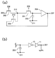
본 실시형태에서 개시하는 RFID 태그는, 제 1 트랜지스터(201), 제 2 트랜지스터(202), 용량(203), 버퍼(204), 제 3 트랜지스터(205)를 가지는 회로를 가진다 (도 1a). 206은 입력 단자, 207은 출력 단자를 나타낸다. 208 내지 210은 각각 제어 단자를 나타낸다. 211은 기준 전압 단자를 나타낸다. The RFID tag disclosed in this embodiment has a circuit including a
제 1 트랜지스터(201), 제 2 트랜지스터(202), 제 3 트랜지스터(205)는 각각 N형 트랜지스터 또는 P형 트랜지스터이다. 버퍼(204)는 예를 들어 제 1 인버터(10)와 제 2 인버터(11)를 직렬로 접속한 회로로 이루어진다(도 1b). The
제 2 트랜지스터(202)의 게이트는 제어 단자(208)에 전기적으로 접속된다. 소스 및 드레인의 한쪽은 입력 단자(206)에 전기적으로 접속된다. 소스 및 드레인의 다른쪽은, 제 1 트랜지스터(201)의 소스 및 드레인의 한쪽 또는 제 3 트랜지스터(205)의 소스 및 드레인의 한쪽에 전기적으로 접속된다. The gate of the
제 1 트랜지스터(201)의 게이트는 제어 단자(209)에 전기적으로 접속된다. 소스 및 드레인의 다른쪽은 용량(203)의 한쪽의 전극 또한 버퍼(204)의 입력에 전기적으로 접속된다. The gate of the
용량(203)의 다른쪽의 전극은 기준 전압 단자(211)에 전기적으로 접속된다. The other electrode of the
버퍼(204)의 출력은 출력 단자(207) 및 제 3 트랜지스터(205)의 소스 및 드레인의 다른쪽에 전기적으로 접속된다. The output of the
제 3 트랜지스터(205)의 게이트는 제어 단자(210)에 전기적으로 접속된다. The gate of the
다음에 동작을 설명한다. 본 실시형태에 있어서 정보 "1"을 전압이 높다고 하고, "0"을 전압이 낮다고 한다. Next, the operation will be described. In this embodiment, the information "1" is said to be high in voltage, and "0" is said to be low in voltage.
(초기 상태)(Initial state)
초기 상태에서는, 제 1 트랜지스터(201), 제 2 트랜지스터(202), 제 3 트랜지스터(205)는 오프이다. 용량(203)에는 전하가 축적되어 있지 않다. 버퍼(204)의 출력은 "0"이며, 출력 단자(207)의 출력 정보는 "0"이다(도 2). In the initial state, the
(출력 정보를 "1"로 하는 경우) (When the output information is set to "1")
용량(203)에 전하를 축적하고, 버퍼(204)의 출력을 "1"로 하여 출력 단자(207)의 출력 정보를 "1"로 하는 경우를 설명한다. The case where charge is accumulated in the
제어 단자(208)로부터의 전압에 의해 제 2 트랜지스터(202)가 온으로 된다. 또 제어 단자(209)로부터의 전압에 의해 제 1 트랜지스터(201)가 온으로 된다. 그리고 입력 단자(206)로부터 고전압 "1"에 대응하는 전류가 흘러 용량(203)에 전하가 축적된다. The
용량(203)에 전하가 축적되면 버퍼(204)의 출력은 "1"로 되고, 출력 단자(207)의 출력 정보는 "1"로 된다(도 3a). When charge is accumulated in the
출력 단자(207)의 출력 정보가 "1"로 되면, 제어 단자(208)로부터의 전압에 의해 제 2 트랜지스터(202)가 오프로 되고, 제어 단자(209)로부터의 전압에 의해 제 1 트랜지스터(201)가 오프로 된다. 또 제어 단자(210)로부터의 전압에 의해 제 3 트랜지스터(205)가 온으로 되고, 버퍼(204)의 출력 전압("1")이 제 2 트랜지스터(202) 및 제 1 트랜지스터(201) 사이의 노드(212)에 인가된다. 노드(212)에는 버퍼(204)의 출력 전압("1")이 인가되므로 용량(203)에 축적된 전하는 제 1 트랜지스터(201)의 소스 드레인을 경유하여 누설되지 않고, 용량(203)에 보유된다(도 3b). 따라서 리플레쉬는 불필요하다. When the output information of the
또 용량(203)은 충분히 큰 용량을 가지고 있는 것이 바람직하다. 예를 들어, 전파가 일시적으로 도중에 끊어지는 등에 의해 전원 전압을 유지할 수 없게 되고, 제 1 트랜지스터(201), 제 2 트랜지스터(202), 제 3 트랜지스터(205) 및 버퍼(204)가 오프로 된 경우를 생각한다. 이 때 용량(203)이 충분히 큰 용량을 가지고 있으면, 용량(203)에 축적된 전하는, 버퍼(204)의 출력("1")이 변화되지 않을 정도로, 일시적으로 보유된다. 그 후, 전력이 공급되어 전원 전압이 회복되면, 버퍼(204)가 온으로 된다. 용량(203)에는 전하가 축적되어 있으므로, 버퍼(204)의 출력은 "1"로 되고, 출력 단자(207)의 출력 정보는 "1"로 된다. In addition, the
(출력 정보를 "0"으로 하는 경우)(When the output information is set to "0")
용량(203)에 축적된 전하를 방출하고, 버퍼(204)의 출력을 "0"으로 하여 출력 단자(207)의 출력 정보를 "0"으로 하는 경우를 설명한다. The case where the charge accumulated in the
입력 단자(206)에는 저전압 "0"이 인가된다. 제어 단자(208)로부터의 전압에 의해 제 2 트랜지스터(202)가 온으로 된다. 또 제어 단자(209)로부터의 전압에 의해 제 1 트랜지스터(201)가 온으로 된다. 노드(212)의 전위는 제 1 트랜지스터(201)의 소스 및 드레인의 한쪽이며, 용량(203)과 전기적으로 접속되어 있는 측의 전위보다도 낮아진다. 용량(203)에 축적된 전하는 제 1 트랜지스터(201)의 소스 드레인을 경유하여 제 1 트랜지스터(201)의 노드(212)측으로 추출된다(도 4a). The low voltage "0" is applied to the
전하가 방출되면, 버퍼(204)의 출력은 "0"으로 되고, 출력 단자(207)의 출력 정보는 "0"으로 된다(도 4b). When charge is released, the output of the
출력 단자(207)의 출력 정보가 "0"으로 되면, 제어 단자(208)로부터의 전압에 의해 제 2 트랜지스터(202)가 오프로 되고, 제어 단자(209)로부터의 전압에 의해 제 1 트랜지스터(201)가 오프로 된다. 또 제어 단자(210)로부터의 전압에 의해 제 3 트랜지스터(205)가 온으로 된다. 용량(203)에 전하는 축적되어 있지 않고, 노드(212)에는 버퍼(204)의 출력 전압("0")이 인가되므로 누설 전류의 문제는 발생하지 않는다. 따라서 리플레쉬는 불필요하다. When the output information of the
또 용량(203)이 충분히 큰 용량을 가지고 있으면, 전파가 일시적으로 도중에 끊어지는 등에 의해 전원 전압을 유지할 수 없게 되고, 버퍼(204)가 오프로 되어도, 전하가 용량(203)에 축적되어 있지 않는 상태는, 버퍼(204)의 출력("0")이 변화되지 않을 정도로, 일시적으로 보유된다. 그 후, 전력이 공급되어 전원 전압이 회복되면, 버퍼(204)가 온으로 된다. 용량(203)에는 전하가 축적되어 있지 않으므로, 버퍼(204)의 출력은 "0"으로 되고, 출력 단자(207)의 출력 정보는 "0"으로 된다. In addition, if the
RFID 태그는, 리플레쉬를 필요로 하지 않고, 제 1 트랜지스터(201)와 용량(203)에 의해 정보를 기억할 수 있다. The RFID tag can store information by the
(실시형태 2)(Embodiment 2)
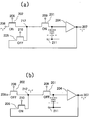
본 실시형태에서 개시하는 RFID 태그는, 제 1 인버터(303), 제 2 인버터(304), 제 1 트랜지스터(307), 용량(308), 버퍼(309), 제 1 아날로그 스위치(305), 제 2 아날로그 스위치(306)를 가지는 회로를 가진다. 301, 302는 각각 입력 단자, 310은 출력 단자를 나타낸다. 312는 기준 전압 단자를 나타낸다(도 5a). The RFID tag disclosed in this embodiment includes a
제 1 트랜지스터(307)는 N형 트랜지스터 또는 P형 트랜지스터이다. 이하, 제 1 트랜지스터(307)는 N형 트랜지스터로서 설명한다. 또 제 1 트랜지스터(307)가 P형 트랜지스터인 경우는 N형 트랜지스터의 경우와 반대의 레벨의 전압이 입력 단자(301)에 인가된다. The
버퍼(309)는 예를 들어 제 3 인버터(12)와 제 4 인버터(13)를 직렬로 접속한 회로로 이루어진다(도 5b). The
입력 단자(301)는 제 1 인버터(303)의 입력에 전기적으로 접속된다. 제 1 인버터(303)의 출력은 제 2 인버터(304)의 입력, 제 1 아날로그 스위치(305)의 제 2 제어 단자(314) 및 제 2 아날로그 스위치(306)의 제 1 제어 단자(315)에 전기적으로 접속된다. 제 2 인버터(304)의 출력은 제 1 아날로그 스위치(305)의 제 1 제어 단자(313), 제 2 아날로그 스위치(306)의 제 2 제어 단자(316) 및 제 1 트랜지스터(307)의 게이트에 전기적으로 접속된다. The
입력 단자(302)는 제 1 아날로그 스위치(305)의 입력에 전기적으로 접속된다. 제 1 아날로그 스위치(305)의 출력은 제 1 트랜지스터(307)의 소스 및 드레인의 한쪽 또는 제 2 아날로그 스위치(306)의 출력에 전기적으로 접속된다. The
제 1 트랜지스터(307)의 소스 및 드레인의 다른쪽은, 용량(308)의 한쪽의 전극 및 버퍼(309)의 입력에 전기적으로 접속된다. The other of the source and the drain of the
용량(308)의 다른쪽의 전극은 기준 전압 단자(312)에 전기적으로 접속된다. The other electrode of the
버퍼(309)의 출력은 출력 단자(310) 및 제 2 아날로그 스위치(306)의 입력에 전기적으로 접속된다. The output of the
다음에 동작을 설명한다. 본 실시형태에 있어서 정보 "1"을 전압이 높다고 하고, "0"을 전압이 낮다고 한다. Next, the operation will be described. In this embodiment, the information "1" is said to be high in voltage, and "0" is said to be low in voltage.
(초기 상태)(Initial state)
초기 상태에서는, 입력 단자(301) 및 입력 단자(302)는 모두 저전압 "0"이 인가되고, 제 1 트랜지스터(307)는 오프이다. 용량(308)에는 전하가 축적되어 있지 않다. 버퍼(309)의 출력은 "0"이며, 출력 단자(310)의 출력 정보는 "0"이다(도 6). In the initial state, the low voltage " 0 " is applied to both the
(출력 정보를 "1"로 하는 경우)(When the output information is set to "1")
용량(308)에 전하를 축적하고, 버퍼(309)의 출력을 "1"로 하여 출력 단자(310)의 출력 정보를 "1"로 하는 경우를 설명한다. The case where charge is accumulated in the
입력 단자(301) 및 입력 단자(302)는 모두 고전압 "1"이 인가된다. 제 1 인버터(303)의 출력은 저전압 "0"이 되고, 제 2 인버터(304)의 출력이 고전압 "1"이 된다. 제 1 아날로그 스위치(305)가 온으로 되고, 고전압 "1"을 출력한다. 또 제 1 트랜지스터(307)가 온으로 되고, 제 1 아날로그 스위치(305)의 출력에 대응하는 전류가 흘러 용량(308)에 전하가 축적된다. 제 2 아날로그 스위치(306)는 오프이다. The
용량(308)에 전하가 축적되면 버퍼(309)의 출력은 "1"로 되고, 출력 단자(310)의 출력 정보는 "1"로 된다(도 7a). When charge is accumulated in the
출력 단자(310)의 출력 정보가 "1"로 되면, 입력 단자(301) 및 입력 단자(302)는 모두 저전압 "0"이 인가된다. 제 1 인버터(303)의 출력은 고전압 "1"이 되고, 제 2 인버터(304)의 출력이 저전압 "0"이 된다. 제 1 트랜지스터(307)가 오프로 된다. 제 1 아날로그 스위치(305)가 오프로 되고, 제 2 아날로그 스위치(306)가 온으로 되고, 버퍼(309)의 출력 전압("1")이 노드(311)에 인가된다. 노드(311)에는 버퍼(309)의 출력 전압("1")이 인가되므로 용량(308)에 축적된 전하는 제 1 트랜지스터(307)의 소스 드레인을 경유하여 누설되지 않고, 보유된다(도 7b). 따라서 리플레쉬는 불필요하다. When the output information of the
그 후, 전파가 일시적으로 도중에 끊어지는 등에 의해 전원 전압을 유지할 수 없게 되어, 제 1 인버터(303), 제 2 인버터(304), 제 1 트랜지스터(307), 제 1 아날로그 스위치(305), 제 2 아날로그 스위치(306) 및 버퍼(309)가 오프로 되는 경우가 있기 때문에, 용량(308)은 충분히 큰 용량을 가지고 있는 것이 바람직하다. 용량(308)이 충분히 큰 용량을 가지고 있으면, 용량(308)에 축적된 전하는, 버퍼(309)의 출력("1")이 변화되지 않을 정도로, 일시적으로 보유된다. 그 후, 전력이 공급되어 전원 전압이 회복되면, 버퍼(309)가 온으로 된다. 용량(308)에는 전하가 축적되어 있으므로, 버퍼(309)의 출력은 "1"로 되고, 출력 단자(310)의 출력 정보는 "1"로 된다. Thereafter, the power supply voltage cannot be maintained due to the temporary interruption of radio waves, and the
또 전력이 공급되어 전원 전압이 회복되고, 입력 단자(301) 및 입력 단자(302)가 함께 초기 상태의 저전압 "0"이 인가된 경우, 제 1 아날로그 스위치(305) 및 제 1 트랜지스터(307)는 오프, 제 2 아날로그 스위치(306)에 온으로 된다. 노드(311)에는 버퍼(309)의 출력 전압("1")이 인가되므로 용량(308)에 축적된 전하는 제 1 트랜지스터(307)의 소스 드레인을 경유하여 누설되는 일이 없으며, 보유된다. 따라서 리플레쉬는 불필요하다. When the power is supplied to restore the power supply voltage and the low voltage " 0 " of the initial state is applied together with the
(출력 정보를 "0"으로 하는 경우) (When the output information is set to "0")
용량(308)에 축적된 전하를 방출하고, 버퍼(309)의 출력을 "0"으로 하여 출력 단자(310)의 출력 정보를 "0"으로 하는 경우를 설명한다. The case where the charge accumulated in the
입력 단자(301)에는 고전압 "1"이 인가되고, 입력 단자(302)에는 저전압 "0"이 인가된다. 제 1 인버터(303)의 출력은 저전압 "0"이 되고, 제 2 인버터(304)의 출력이 고전압 "1"이 된다. 제 1 트랜지스터(307)가 온으로 된다. 제 1 아날로그 스위치(305)가 온으로 된다. 노드(311)의 전위는 제 1 트랜지스터(307)의 소스 및 드레인의 한쪽이며, 용량(308)과 전기적으로 접속되어 있는 측의 전위보다도 낮아진다. 용량(308)에 축적된 전하는 제 1 트랜지스터(307)의 소스 드레인을 경유하여 제 1 트랜지스터(307)의 노드(311)측으로 방출된다(도 8a). 제 2 아날로그 스위치(306)는 오프이다. A high voltage "1" is applied to the
전하가 방출되면, 버퍼(309)의 출력은 "0"이 되고, 출력 단자(310)의 출력 정보는 "0"으로 된다(도 8b). When charge is released, the output of the
출력 단자(310)의 출력 정보가 "0"으로 되면, 입력 단자(301)에는 저전압 "0"이 인가되고, 제 1 트랜지스터(307)가 오프로 된다. 용량(308)에 전하는 축적되어 있지 않고, 노드(311)에는 버퍼(309)의 출력 전압("0")이 인가되므로 누설 전류의 문제는 발생하지 않는다. 따라서 리플레쉬는 불필요하다. When the output information of the
또 전파가 일시적으로 도중에 끊어지는 등에 의해 전원 전압을 유지할 수 없게 되고, 버퍼(309)가 오프로 되어도, 용량(308)이 충분히 큰 용량을 가지고 있으면, 전하가 용량(308)에 축적되어 있지 않는 상태는, 버퍼(309)의 출력("0")이 변화되지 않을 정도로, 일시적으로 보유된다. 그 후, 전력이 공급되어 전원 전압이 회복되면, 버퍼(309)가 온으로 된다. 용량(308)에는 전하가 축적되어 있지 않으므로, 버퍼(309)의 출력은 "0"이 되고, 출력 단자(310)의 출력 정보는 "0"으로 된다. If the power supply voltage cannot be maintained due to a temporary interruption of the radio wave, and the
또 전력이 공급되어 전원 전압이 회복되고, 입력 단자(301) 및 입력 단자(302)가 함께 초기 상태의 저전압 "0"이 인가된 경우, 제 1 아날로그 스위치(305) 및 제 1 트랜지스터(307)는 오프, 제 2 아날로그 스위치(306)에 온으로 된다. 용량(308)에 전하는 축적되어 있지 않고, 노드(311)에는 버퍼(309)의 출력 전압("0")이 인가되므로 누설 전류의 문제는 발생하지 않는다. 따라서 리플레쉬는 불필요하다. When the power is supplied to restore the power supply voltage and the low voltage " 0 " of the initial state is applied together with the
RFID 태그는, 리플레쉬를 필요로 하지 않고, 제 1 트랜지스터(307)와 용량(308)에 의해 정보를 기억할 수 있다. The RFID tag can store information by the
(실시형태 3)(Embodiment 3)
본 실시형태에서 개시하는 RFID 태그(400)는 안테나(401), 정류 회로(402), 로직부(403) 및 플래그 보유 회로(404)를 가진다(도 9). The RFID tag 400 disclosed in this embodiment has an antenna 401, a
안테나(401)는, 리더/라이터의 교신에 있어서 아날로그 신호의 송수신을 행한다. The antenna 401 transmits and receives an analog signal in communication between a reader and a writer.
안테나(401)에는 정류 회로(402)가 접속된다. 정류 회로(402)는 안테나(401)를 통하여 리더/라이터로부터 출력된 전파의 전력을 정류하여 전원 전압 VDD로서 출력한다. The
정류 회로(402)가 정류한 전원 전압 VDD는, 로직부(403), 및 플래그 보유 회로(404)에 각각 공급된다. 로직부(403)는, 클록 회로, 논리 회로, 변조 회로 및 복조 회로를 가진다. The power supply voltage VDD rectified by the
클록 회로는, 클록 신호를 생성하고, 논리 회로에 공급한다. 복조 회로는, 안테나가 수신한 아날로그 신호를 디지털 신호로 복조하여 논리 회로에 출력한다. 변조 회로는, 상기 논리 회로로 출력된 디지털 신호를 아날로그 신호로 변조하여 안테나를 통하여 리더/라이터에 송신한다. The clock circuit generates a clock signal and supplies it to the logic circuit. The demodulation circuit demodulates the analog signal received by the antenna into a digital signal and outputs it to the logic circuit. The modulation circuit modulates the digital signal output to the logic circuit into an analog signal and transmits the digital signal to the reader / writer through the antenna.
논리 회로는 메모리를 가진다. 또 논리 회로는 메모리에 축적된 정보를 판독하고, 메모리에 정보를 기록한다. The logic circuit has a memory. The logic circuit reads the information accumulated in the memory and writes the information to the memory.
플래그 보유 회로(404)는 상기 실시형태 1 또는 2의 회로를 가진다. The
실시형태 1에 나타낸 회로는, 제 1 트랜지스터(201), 제 2 트랜지스터(202), 용량(203), 버퍼(204), 제 3 트랜지스터(205)를 가진다(도 1). The circuit shown in
제 1 트랜지스터의 제어 단자(209), 제 2 트랜지스터의 제어 단자(208), 제 3 트랜지스터의 제어 단자(210) 및 입력 단자(206) 각각은, 로직부(403)의 논리 회로로의 출력에 의해 제어된다. 출력 단자(207)는 로직부(403)의 논리 회로에 입력된다. Each of the
플래그 보유 회로(404)로의 전원 전압 VDD는 정류 회로(402)로부터 공급된다. 또는 로직부(403)를 경유하여 정류 회로(402)로부터 공급된다. 구체적으로는 버퍼(204)의 전원 전압 VDD는 정류 회로(402)로부터 공급된다. 또는 로직부(403)를 경유하여 정류 회로(402)로부터 공급된다. The power supply voltage VDD to the
실시형태 1에 나타낸 회로를 가지는 플래그 보유 회로(404)는, 제 1 트랜지스터(201)와 용량(203)에 의해 정보(전하)를 기억할 수 있다. 따라서 리플레쉬는 불필요하다. 또 용량(203)이 충분히 큰 용량을 가지고 있으면, 정류 회로(402)로부터의 전원 전압 VDD가 공급 정지가 되었을 때에도 용량(203)에 축적된 전하는, 버퍼(204)의 출력이 변화되지 않을 정도로, 일시적으로 보유된다. 따라서 한번 판독한 정보를 다시 판독하는 것을 방지하는 세션 플래그의 상태를 보유할 수 있다. The
또 실시형태 2에 나타낸 회로는, 제 1 인버터(303), 제 2 인버터(304), 제 1 트랜지스터(307), 용량(308), 버퍼(309), 제 1 아날로그 스위치(305), 제 2 아날로그 스위치(306)를 가진다(도 5). In addition, the circuit shown in the second embodiment includes the
입력 단자(301) 및 입력 단자(302) 각각은, 로직부(403)의 논리 회로로부터의 출력에 의해 제어된다. 출력 단자(310)는 로직부(403)의 논리 회로에 입력된다. Each of the
상기와 마찬가지로 플래그 보유 회로(404)로의 전원 전압 VDD는 정류 회로(402)로부터 공급된다. 또는 로직부(403)를 경유하여 정류 회로(402)로부터 공급된다. 구체적으로는 제 1 인버터(303)의 전원 전압 VDD, 제 2 인버터(304)의 전원 전압 VDD, 버퍼(309)의 전원 전압 VDD, 제 1 아날로그 스위치(305)의 전원 전압 VDD, 제 2 아날로그 스위치(306)의 전원 전압 VDD는 정류 회로(402)로부터 공급된다. 또는 로직부(403)를 경유하여 정류 회로(402)로부터 공급된다. As described above, the power supply voltage VDD to the
실시형태 2에 나타낸 RFID 태그를 가지는 플래그 보유 회로(404)는, 제 1 트랜지스터(307)와 용량(308)에 의해 정보(전하)를 기억할 수 있다. 따라서 리플레쉬는 불필요하다. 또 용량(308)이 충분히 큰 용량을 가지고 있으면, 정류 회로(402)로부터의 전원 전압 VDD가 공급 정지가 되었을 때에도 용량(308)에 축적된 전하는, 버퍼(309)의 출력이 변화되지 않을 정도로, 일시적으로 보유된다. 따라서 한번 판독한 정보를 다시 판독하는 것을 방지하는 세션 플래그의 상태를 보유할 수 있다. The
(실시형태 4)(Embodiment 4)
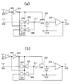
본 실시형태에서는 실시형태 3과 다른 구성을 가지는 RFID 태그를 설명한다. In this embodiment, an RFID tag having a configuration different from that of the third embodiment will be described.
본 실시형태에서 나타내는 RFID 태그(500)는, 안테나 회로(501) 및 신호 처리 회로(502)를 가진다. 신호 처리 회로(502)는, 정류 회로(503), 전원 회로(504), 복조 회로(505), 발진 회로(506), 논리 회로(507), 메모리 컨트롤 회로(508), 메모리 회로(509), 논리 회로(510), 앰프(511), 변조 회로(512)를 가진다(도 10). 메모리 회로(509)는 상기 실시형태 1 및 2의 회로를 가진다. The
안테나 회로(501)에 의해 수신된 통신 신호는 복조 회로(505)에 입력된다. 수신되는 통신 신호, 즉 안테나 회로(501)와 리더/라이터 간에서 송수신 되는 신호의 주파수는 극초단파대에 있어서는 915MHz, 2.45GHz 등이 있고, 각각 ISO 규격 등으로 규정된다. 물론, 안테나 회로(501)와 리더/라이터 간에서 송수신되는 신호의 주파수는 이것에 한정되지 않고, 예를 들어 서브밀리파인 300GHz 내지 3THz, 밀리파인 30GHz 내지 300GHz, 마이크로파인 3GHz 내지 30GHz, 극초단파인 300MHz 내지 3GHz, 초단파인 30MHz 내지 300MHz의 어느 주파수라도 사용할 수 있다. 또한, 안테나 회로(501)와 리더/라이터 간에서 송수신되는 신호는, 반송파를 변조한 신호이다. 반송파의 변조 방식은, 아날로그 변조 또는 디지털 변조이며, 진폭 변조, 위상 변조, 주파수 변조 및 스펙트럼 확산의 어느 하나라도 좋다. 바람직하게는, 진폭 변조 또는 주파수 변조이다. The communication signal received by the
발진 회로(506)로부터 출력된 발진 신호는, 클록 신호로서 논리 회로(507)에 공급된다. 또한, 변조된 반송파는 복조 회로(505)에서 복조된다. 복조후의 신호도 논리 회로(507)에 보내져 해석된다. 논리 회로(507)에서 해석된 신호는 메모리 컨트롤 회로(508)에 보내진다. 메모리 컨트롤 회로(508)는 메모리 회로(509)를 제어하고, 메모리 회로(509)에 기억된 데이터를 추출하고, 논리 회로(510)에 보낸다. 논리 회로(510)에 보내진 신호는 논리 회로(510)에서 인코드 처리된 후 앰프(511)에서 증폭되고, 그 신호에 의해 변조 회로(512)는 반송파를 변조한다. 이 변조된 반송파에 의해 리더/라이터가 RFID 태그로부터의 신호를 인식한다. The oscillation signal output from the
정류 회로(503)에 입력된 반송파는 정류된 후, 전원 회로(504)에 입력된다. 이렇게 하여 얻어진 전원 전압을 전원 회로(504)로부터 복조 회로(505), 발진 회로(506), 논리 회로(507), 메모리 컨트롤 회로(508), 메모리 회로(509), 논리 회로(510), 앰프(511), 변조 회로(512) 등에 공급한다. The carrier wave input to the
신호 처리 회로(502)와 안테나 회로(501)에 있어서의 안테나와의 접속에 대해서는 특히 한정되지 않는다. 예를 들어 안테나와 신호 처리 회로(502)를 와이어 본딩 접속이나 범프 접속을 사용하여 접속하거나, 또는 칩화한 신호 처리 회로(502)의 일면을 전극으로 하여 안테나에 접착한다. 신호 처리 회로(502)와 안테나의 접착에는 ACF(anisotropic conductive film; 이방성 도전성 필름)를 사용할 수 있다. The connection between the
안테나는, 신호 처리 회로(502)와 함께 동일한 기판 위에 적층하여 설치하거나, 외장형의 안테나를 사용한다. 물론, 신호 처리 회로의 상부 또는 하부에 안테나가 설치된다. The antennas are stacked and installed on the same substrate together with the
정류 회로(503)는, 안테나 회로(501)가 수신하는 반송파에 의해 유도되는 교류 신호를 직류 신호로 변환한다. The
RFID 태그(500)는 배터리(561)를 가져도 좋다(도 11). 정류 회로(503)로부터 출력되는 전원 전압이, 신호 처리 회로(502)를 동작시키기에 충분하지 않을 때에는, 배터리(561)로부터도 신호 처리 회로(502)를 구성하는 각 회로, 예를 들어 복조 회로(505), 발진 회로(506), 논리 회로(507), 메모리 컨트롤 회로(508), 메모리 회로(509), 논리 회로(510), 앰프(511), 변조 회로(512) 등에 전원 전압을 공급한다. The
정류 회로(503)로부터 출력되는 전원 전압 중의 잉여분을 배터리(561)에 충전하면 좋다. RFID 태그(500)에 안테나 회로(501) 및 정류 회로(503)와는 달리 또 안테나 회로 및 정류 회로를 설치함으로써, 무작위로 발생하는 전자파 등으로부터 배터리(561)에 축적하는 에너지를 얻을 수 있다. An excess of the power supply voltage output from the
배터리에 충전함으로써 연속적으로 사용할 수 있다. 배터리는 시트 형으로 형성된 전지를 사용한다. 예를 들어 겔상 전해질을 사용하는 리튬 폴리머 전지나, 리튬 이온 전지, 리튬 이차 전지 등을 사용하면, 배터리의 소형화가 가능하다. 예를 들어 니켈 수소 전지, 니켈 카드륨 전지 등을 들 수 있다. 또는 대용량의 콘덴서 등을 사용한다. The battery can be used continuously by charging. The battery uses a cell formed in sheet form. For example, when a lithium polymer battery using a gel electrolyte, a lithium ion battery, a lithium secondary battery, or the like is used, the battery can be miniaturized. For example, a nickel hydrogen battery, a nickel cadmium battery, etc. are mentioned. Or use a large capacity capacitor.
(실시형태 5)(Embodiment 5)
본 실시형태는 상기 실시형태에서 나타낸 RFID 태그의 일 제작 방법을 설명한다. This embodiment describes one manufacturing method of the RFID tag shown in the above embodiment.
기판(701)의 일 표면에 박리층(702)을 형성하고, 박리층(702) 위에 하지(下地)가 되는 절연막(703) 및 반도체막(704)(예를 들어 비정질 규소를 포함하는 막)을 형성한다(도 12a). 박리층(702), 절연막(703) 및 반도체막(704)은, 연속적으로 형성할 수 있다. 결과적으로, 대기에 노출되지 않기 때문에 불순물의 혼입을 막을 수 있다. The
기판(701)에는 유리 기판, 석영 기판, 금속 기판, 스테인리스 기판, 본 공정의 처리 온도에 견딜 수 있는 플라스틱 기판 등을 사용한다. As the
박리층(702)은, 금속막이나 금속막과 금속 산화막의 적층층을 사용한다. The
금속막은 텅스텐(W), 몰리브덴(Mo), 티타늄(Ti), 탄탈(Ta), 니오브(Nb), 니켈(Ni), 코발트(Co), 지르코늄(Zr), 아연(Zn), 루테늄(Ru), 로듐(Rh), 팔라듐(Pd), 오즈뮴(Os), 이리듐(Ir)으로부터 선택된 원소, 상기 원소를 주성분으로 하는 합금 재료, 상기 원소를 주성분으로 하는 화합물 재료로 이루어지는 막이며, 단층 또는 적층으로 형성한다. 금속막은 스퍼터링법이나 플라즈마 CVD법 등에 의해 형성한다. Metal films include tungsten (W), molybdenum (Mo), titanium (Ti), tantalum (Ta), niobium (Nb), nickel (Ni), cobalt (Co), zirconium (Zr), zinc (Zn), ruthenium (Ru) ), A film made of an element selected from rhodium (Rh), palladium (Pd), osmium (Os), iridium (Ir), an alloy material containing the element as a main component, and a compound material containing the element as a main layer, It is formed by lamination. The metal film is formed by sputtering, plasma CVD, or the like.
금속막과 금속 산화막의 적층층은, 상술한 금속막을 형성한 후에, 산소 분위기 하 또는 N2O 분위기 하에 있어서의 플라즈마 처리, 산소 분위기 하 또는 N2O 분위기 하에 있어서의 가열 처리에 의해, 금속막 표면에 상기 금속막의 산화물 또는 산화 질화물을 마련하여 형성한다. 또는 금속막을 형성한 후에, 오존수 등의 산화력이 강한 용액으로 표면을 처리함으로써, 금속막 표면에 상기 금속막의 산화물을 마련하여 형성한다. After the metal film and the metal oxide film are laminated, the metal film is formed by plasma treatment in an oxygen atmosphere or an N 2 O atmosphere, heat treatment in an oxygen atmosphere or an N 2 O atmosphere, after forming the metal film described above. It is formed by providing an oxide or oxynitride of the metal film on the surface. Alternatively, after the metal film is formed, the surface of the metal film is provided with an oxide of the metal film by treating the surface with a strong oxidizing solution such as ozone water.
절연막(703)은, 규소의 산화물 또는 규소의 질화물을 포함하는 막이며, 스퍼터링법이나 플라즈마 CVD법 등에 의해, 단층 또는 적층으로 형성한다. 절연막(703)은, 기판(701)으로부터의 불순물의 침입을 방지한다. The insulating
반도체막(704)은, 스퍼터링법, LPCVD법, 플라즈마 CVD법 등에 의해 형성되고, 25nm 이상 200nm 이하 정도, 바람직하게는 50nm 이상 70nm 이하 정도의 두께를 가진다. 반도체막(704)은 예를 들어 비정질 규소막, ZnO를 포함하는 산화물 반도체막이다. The
반도체막(704)에 레이저광을 조사하는 등으로 결정화하여 결정질 반도체막을 형성하여도 좋다. The
반도체막(704)을 원하는 형상으로 에칭하여, 반도체막(704a), 반도체막(704b)을 형성한다. 반도체막(704a), 반도체막(704b)을 덮어 게이트 절연막(705)을 형성한다(도 12b). The
게이트 절연막(705)은, CVD법이나 스퍼터링법 등에 의해, 규소의 산화물 또는 규소의 질화물을 포함하는 막이며, 단층막 또는 적층막이다. The
게이트 절연막(705)은, 반도체막(704a), 반도체막(704b)에 대하여 플라즈마 처리를 행하고, 표면을 산화 또는 질화함으로써 형성하여도 좋다. 예를 들어, He, Ar, Kr, Xe 등의 희가스와, 산소, 산화 질소(예를 들어, NO2), 암모니아, 질소, 수소 등의 혼합 가스를 도입한 플라즈마 처리로 형성한다. 이 경우의 플라즈마의 여기는, 마이크로파를 사용하여 행하면, 저전자 온도로 고밀도의 플라즈마를 생성할 수 있다. 이 고밀도 플라즈마로 생성된 산소 라디칼(OH 라디칼을 포함하는 경우도 있음)이나 질소 라디칼(NH 라디칼을 포함하는 경우도 있음)에 의해, 반도체막의 표면을 산화 또는 질화할 수 있다. The
이러한 고밀도 플라즈마를 사용한 처리에 의해, 1nm 이상 20nm 이하정도, 대표적으로는 5nm 이상 10nm 이하 정도의 절연막이 반도체막에 형성된다. 이 경우의 반응은, 고상 반응이기 때문에, 상기 절연막과 반도체막의 계면 준위 밀도를 극히 낮게 할 수 있다. 이러한, 플라즈마 처리는, 반도체막(결정성 실리콘, 다결정 실리콘, ZnO를 포함하는 산화물 반도체막 등)을 직접 산화(또는 질화)하기 때문에, 형성되는 절연막의 막 두께의 편차를 극히 작게 할 수 있다. 더욱이, 결정성 실리콘의 결정립계에서도 산화가 진행하는 일이 없기 때문에, 매우 바람직하다. By the process using such a high density plasma, the insulating film of 1 nm or more and about 20 nm or less, typically 5 nm or more and about 10 nm or less is formed in a semiconductor film. Since the reaction in this case is a solid phase reaction, the interface state density of the insulating film and the semiconductor film can be made extremely low. Such a plasma process directly oxidizes (or nitrides) a semiconductor film (crystalline silicon, polycrystalline silicon, an oxide semiconductor film containing ZnO, etc.), so that the variation in the film thickness of the formed insulating film can be made extremely small. Moreover, since oxidation does not advance even in the grain boundary of crystalline silicon, it is very preferable.
게이트 절연막(705)은, 플라즈마 처리에 의해 형성되는 절연막만을 사용하거나, 또는 그것에 더하여 플라즈마나 열 반응을 이용한 CVD법으로 산화 규소, 산질화 규소, 질화 규소 등의 절연막을 퇴적하여 형성한다. 플라즈마 처리에 의해 형성한 게이트 절연막을 포함하는 트랜지스터는 특성의 편차가 작다. The
게이트 절연막(705) 위에 도전막을 형성한다. 100nm 이상 500nm 이하 정도의 두께의 도전막을 단층으로 형성한다. 탄탈(Ta), 텅스텐(W), 티타늄(Ti), 몰리브덴(Mo), 알루미늄(Al), 구리(Cu), 크롬(Cr), 니오브(Nb) 등으로부터 선택된 원소를 포함하는 재료, 이들의 원소를 주성분으로 하는 합금 재료, 또는 이들의 원소를 주성분으로 하는 화합물 재료를 사용한다. 인 등의 불순물 원소를 첨가한 다결정 규소로 대표되는 반도체 재료를 사용하여도 좋다. 예를 들어, 질화 탄탈막과 텅스텐막의 적층막, 질화 텅스텐막과 텅스텐 막의 적층막, 질화 몰리브덴막과 몰리브덴막의 적층막을 사용한다. A conductive film is formed over the
상기 도전막 위에, 포토리소그래피법을 사용하여 레지스트로 이루어지는 마스크를 형성하고, 에칭 처리를 행하고, 반도체막(704a), 반도체막(704b)의 상방에 게이트 전극(707)을 형성한다. On the said conductive film, the mask which consists of resists is formed using the photolithographic method, an etching process is performed, and the
게이트 전극(707)을 마스크로 하여, 반도체막(704a), 반도체막(704b)에, 이온 도프법 또는 이온 주입법에 의해, n형 또는 p형을 부여하는 불순물 원소를 저농도로 첨가한다. 본 실시형태에 있어서는, 반도체막(704a), 반도체막(704b)에, n형을 부여하는 불순물 원소를 저농도로 첨가한다. n형을 부여하는 불순물 원소는, 15족에 속하는 원소이며, 인(P), 비소(As) 등이다. p형을 부여하는 불순물 원소는, 13족에 속하는 원소이며, 붕소(B) 등이다. Using the
본 실시형태는 n형 TFT를 나타내고 있지만, n형 TFT에 한정하여 해석되지 않는다. p형 TFT만을 형성하여도 좋다. 또한, n형 TFT와 p형 TFT를 아울러 형성하여도 좋다. Although this embodiment shows an n-type TFT, it is not interpreted only to n-type TFT. Only the p-type TFT may be formed. In addition, the n-type TFT and the p-type TFT may be formed together.
게이트 절연막(705)과 게이트 전극(707)을 덮도록, 절연막을 형성한다. 절연막은, 플라즈마 CVD법이나 스퍼터링법 등에 의해 형성하는 규소, 규소의 산화물 또는 규소의 질화물의 무기 재료를 포함하는 막이다. An insulating film is formed to cover the
절연막을 이방성 에칭에 의해 선택적으로 에칭하여, 게이트 전극(707)의 측면에 접하는 절연막(708)(사이드월이라고도 함)을 형성한다. 절연막(708)은 LDD(Lightly Doped Drain) 영역을 형성할 때에 마스크로서 사용한다. The insulating film is selectively etched by anisotropic etching to form an insulating film 708 (also called sidewall) in contact with the side surface of the
포토리소그래피법이 의해 형성한 레지스트로 이루어지는 마스크와, 게이트 전극(707) 및 절연막(708)을 마스크로서 사용하고, 반도체막(704a), 반도체막(704b)에 n형을 부여하는 불순물 원소를 첨가한다. 이로써, 채널 형성 영역(706a), 제 1 불순물 영역(706b), 제 2 불순물 영역(706c)이 형성된다(도 12c). 제 1 불순물 영역(706b)은 박막 트랜지스터의 소스 영역 또는 드레인 영역이며, 제 2 불순물 영역(706c)은 LDD 영역이다. 제 2 불순물 영역(706c)이 포함하는 불순물 원소의 농도는, 제 1 불순물 영역(706b)이 포함하는 불순물 원소의 농도보다도 낮다. Using a mask made of a resist formed by the photolithography method and a
계속하여, 게이트 전극(707), 절연막(708) 등을 덮도록, 절연막을 형성한다. 본 실시형태에서는 절연막은 절연막(709, 710, 711)의 3층막이다. 절연막은 CVD법 등에 의해 형성한다. 절연막(709, 710)은, 규소, 규소의 산화물 또는 규소의 질화물의 무기 재료를 포함하는 막이며, 절연막(711)은 유기수지 등의 유기재료를 포함하는 막이다. Subsequently, an insulating film is formed to cover the
절연막(709, 710, 711)을 에칭하여, 제 1 불순물 영역(706b)에 도달하는 콘택트 홀을 형성한 후, 박막 트랜지스터의 소스 전극 또는 드레인 전극으로서 기능하는 도전막(731a), 및 접속 배선으로서 기능하는 도전막(731b)을 형성한다. 도전막(731a, 731b)은, 콘택트 홀을 충전하도록 도전막을 형성하고, 상기 도전막을 선택적으로 에칭함으로써 형성한다. 또, 도전막을 형성하기 전에, 콘택트 홀에 있어서 노출된 반도체막(704a), 반도체막(704b)의 표면에 실리사이드를 형성하고, 저항을 낮게 하여도 좋다. 도전막(731a, 731b)은, 저저항 재료를 사용하여 형성하면 신호 지연을 발생하지 않아, 바람직하다. 저저항 재료는 내열성이 낮은 경우도 많이 있기 때문에, 저저항 재료의 상하에는 내열성이 높은 재료를 형성하면 좋다. 도전막(731a, 731b)은, CVD법이나 스퍼터링법 등에 의해 형성한다. The insulating
이상에 의해, 박막 트랜지스터(730a), 박막 트랜지스터(730b)를 포함하는 소자층(749)이 얻어진다(도 13a). 박막 트랜지스터(730a), 박막 트랜지스터(730b)는 실시형태 1, 2에 나타낸 트랜지스터에 사용할 수 있다. By the above, the
절연막(709, 710, 711)을 형성하기 전, 또는 절연막(709)을 형성한 후, 또는 절연막(709, 710)을 형성한 후에, 반도체막(704)의 결정성의 회복이나 반도체막(704)에 첨가된 불순물 원소의 활성화, 반도체막(704)의 수소화를 목적으로 한 가열 처리를 행하면 좋다. 가열 처리에는, 열 어닐법, 레이저 어닐법, RTA법 등을 적용한다. Before the formation of the insulating
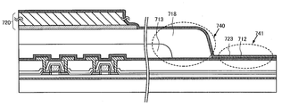
도전막(731a, 731b)을 덮도록, 절연막(712, 713)을 형성한다(도 13b). 절연막(712)에는 50 내지 150nm, 예를 들어 100nm의 막 두께를 가지는 질화규소막을 사용하고, 절연막(713)에는 1000 내지 2000nm, 예를 들어 1500nm의 막 두께를 가지는 폴리이미드막을 사용한다. 절연막(713)의 표면 형상은 평탄성이 높으면 바람직하다. 질화규소막 대신에 산화 질화 규소막이나 질화 산화 규소막을 사용하여도 좋다. 폴리이미드막 대신에 폴리아미드, 벤조시클로부텐, 아크릴, 에폭시 등의 유기재료나 실록산 재료 등을 사용하여도 좋다. 절연막(712, 713)은, CVD법, 스퍼터링법, SOG법, 액적 토출법 또는 스크린 인쇄법 등에 의해 작성한다. The insulating
절연막(712, 713)에 개구부를 형성한다. 구체적으로는 접속 배선(731b)이 노출되는 개구부(714)를 형성한다. 이러한 개구부(714)에 있어서(상세하게는 점선으로 둘러싸인 영역(715)에 있어서), 절연막(712)의 단부는, 절연막(713)으로 덮여 있다. 상층의 절연막(713)으로 하층의 절연막(712)의 단부를 덮음으로써, 그 후 개구부(714)에 형성되는 배선의 단절(段切)을 방지할 수 있다. 본 실시형태에서는, 절연막(713)이 유기재료인 폴리이미드를 사용하고 있기 때문에, 개구부(714)에 있어서, 절연막(713)은 완만한 테이퍼를 가질 수 있어, 효율적으로 단절을 방지할 수 있다. Openings are formed in the insulating
절연막(713) 위에 도전막(717)을 형성하고, 도전막(717) 위에 절연막(718)을 형성한다(도 13c). A
도전막(717)은, 도전막(731a, 731b)과 동일한 재료로 형성할 수 있다. 도전막(717)은, 박막 트랜지스터와, 안테나 사이의 신호에 기초하는 전류가 흐르기 때문에, 도전 재료, 예를 들어 알루미늄으로 형성한다. 도전막(717)은, CVD법이나 스퍼터링법 등에 의해 형성한다. 절연막(718)은, 그 표면 형상에 평탄성이 요구되기 때문에, 유기 재료로 형성하면 좋고, 1000 내지 3000nm, 예를 들어 2000nm의 막 두께의 폴리이미드를 사용하는 경우를 예시한다. The
절연막(718)은 절연막(713)의 개구부(714), 및 개구부(714)에 형성된 도전막(717)의 표면의 요철을 평탄하게 할 필요가 있고, 절연막(713)의 막 두께보다도 두꺼운, 예를 들어 2000nm의 막 두께로 형성한다. The insulating
도 14에 반도체 장치의 주변부를 도시한다. 절연막(718)은, 회로부에 있어서의 안테나의 외측(구체적으로는 영역(740))에서, 절연막(713)의 단부를 덮으면 바람직하다. 수분이나 산소의 침입을 방지할 수 있다. 14 shows the periphery of the semiconductor device. The insulating
절연막(718) 위에 안테나(720)를 형성한다(도 15a). 안테나(720)와 도전막(717)을 개구부를 사이에 두고 접속시킨다(도시하지 않음). An
안테나(720)는, 제 1 도전막(721), 제 2 도전막(722)의 적층막이며, 본 실시형태에서는, 제 1 도전막(721)으로서, 두께 50 내지 150nm, 예를 들어 100nm의 티타늄, 제 2 도전막(722)으로서, 두께 4000 내지 6000nm, 예를 들어 5000nm 알루미늄의 적층 구조의 경우를 예시한다. 티타늄은, 안테나의 내습성을 높일 수 있고, 절연막(718)과 안테나(720)의 밀착성을 높일 수도 있다. 또한 티타늄은, 도전막(717)과의 접촉 저항을 낮게 할 수 있다. 본 실시형태에서는 티타늄의 단부보다, 알루미늄의 단부가 내측이 된다(영역(742)). 티타늄 단부로부터 거리L=0.8μm 이상 2μm 이하의 범위에서 내측이 되도록 한다(도 15a). 알루미늄의 막 두께를 티타늄의 막 두께보다도 크게 하고, 티타늄 단부가 알루미늄 단부보다 돌출되어 있음으로써, 그 후에 형성되는 절연막의 단절을 방지할 수 있고, 안테나의 내성을 높일 수 있다. The
안테나는 CVD법, 스퍼터링법, 스크린 인쇄나 그라비아 인쇄 등의 인쇄법, 액적 토출법, 디스펜서법, 도금법 등을 사용하여 형성한다. 또 안테나는 적층막 또는 단층막이다. The antenna is formed using a CVD method, a sputtering method, a printing method such as screen printing or gravure printing, a droplet ejecting method, a dispenser method, a plating method, or the like. The antenna is a laminated film or a single layer film.
안테나(720)를 덮고, 절연막(723)을 형성한다. 본 실시형태에서는, 절연막(723)을 200nm의 질화규소막으로 형성한다. 절연막(723)은 안테나의 내습성을 보다 높인다. 티타늄 단부가 알루미늄 단부보다 돌출되어 있기 때문에, 절연막(723)은 단절되지 않게 형성할 수 있다. 절연막(723)은 산화 질화규소막, 질화산화 규소막 또는 그 밖의 무기 재료막이라도 좋다. The
절연막(723)과, 절연막(712)은, 절연막(718)의 외측, 즉 회로부에 있어서의 안테나의 외측(구체적으로는 영역(741))에서 접하고 있으면 바람직하다(도 14). 절연막(712, 723)은 함께 질화규소막으로 형성하면, 동일 재료끼리가 밀착하는 구성이 되어, 밀착성이 높고, 수분이나 산소의 침입을 방지할 수 있다. 또 질화규소막은, 산화 규소막과 비교하여 치밀성이 높기 때문에, 수분이나 산소의 침입 방지를 효과적으로 방지할 수 있다. 절연막(712, 723)이 밀착하고 있는 영역은 주변 영역이며, 회로부를 둘러싸도록 형성되어 있다. 이러한 주변 영역의 구성을 채용하고 있지 않는 RFID 태그와 비교하여, RFID 태그의 단부로부터의 박리와 같은, 경시적인 형상이나 특성의 변화에 따르는 결함을 적게 할 수 있다. It is preferable that the insulating
절연막(723)을 덮도록 제 1 절연체(751)를 형성한다(도 15b). 제 1 절연체(751)는 섬유체(727)에 유기수지(728)가 함침된 구조체(726)이다. 또 구조체(726)의 표면에는 제 1 충격 완화층(750)이 형성되어 있다. 제 1 충격 완화층(750)은 아라미드 수지층이다. A
섬유체(727)에 유기수지(728)가 함침된 구조체(726)는, 프리프레그라고도 불린다. 프리프레그는, 구체적으로는 섬유체에 매트릭스 수지를 유기용제로 희석한 바니시를 함침시킨 후, 유기용제를 휘발시켜서 매트릭스 수지를 반경화시킨 것이다. 프리프레그는 탄성률 13GPa 이상 15GPa 이하, 파단 계수 140MPa이다. 박막화한 프리프레그는 박형으로 플렉시블 RFID 태그의 제작을 가능하게 한다. 프리프레그의 섬유체의 대표예로서는, 폴리비닐알콜계 섬유, 폴리에스테르계 섬유, 폴리아미드계 섬유, 폴리에틸렌계 섬유, 아라미드계 섬유, 폴리파라페닐렌벤조비스옥사졸 섬유, 유리 섬유, 또는 탄소 섬유 등을 들 수 있다. 유기수지의 대표예로서는, 에폭시 수지, 불포화 폴리에스테르 수지, 폴리이미드 수지 또는 불소 수지 등을 들 수 있다. The
제 1 절연체(751)의 두께는, 5μm 이상 100μm 이하, 또한 10μm 이상 50μm가 바람직하고, 본 실시형태에서는 32μm로 한다. 본 실시형태에서는, 제 1 절연체(751) 중, 구조체(726)의 막 두께를 10 내지 30μm, 예를 들어 20μm로 하고, 제 1 충격 완화층(750)의 막 두께를 5 내지 15μm, 예를 들어 12μm로 한다. 박형으로 플렉시블 RFID 태그를 제작할 수 있다. As for the thickness of the
제 1 충격 완화층(750)을 형성한 후, 제 1 충격 완화층(750)의 표면에 제 1 도전층(729)을 형성한다. 제 1 도전층(729)은 산화 규소와 인듐 주석 산화물의 화합물을 사용한다. 제 1 도전층(729)은 구조체(726)나 제 1 충격 완화층(750)보다 저항이 낮다. 제 1 도전층(729)은, 막형으로 형성하거나, 작은 간격을 둔 섬형상의 덩어리로 형성하여도 좋다. 막 두께는 50nm 이상 200nm 이하로 할 수 있다. 제 1 도전층(729)은 산화 규소와 인듐 주석 산화물의 화합물 이외에, 티타늄, 몰리브덴, 텅스텐, 알루미늄, 구리, 은, 금, 니켈, 주석, 백금, 팔라듐, 이리듐, 로듐, 탄탈, 카드뮴, 아연, 철, 실리콘, 게르마늄, 지르코늄, 바륨 등으로 선택된 원소를 포함하는 재료, 상기 원소를 주성분으로 하는 합금 재료, 상기 원소를 주성분으로 하는 화합물 재료 등을 사용하여 형성할 수 있다. 제 1 도전층(729)은, 스퍼터링법이나 플라즈마 CVD법, 도포법, 인쇄법, 전해 도금법이나 무전해 도금법 등의 도금법을 사용하여 형성한다. 또, 제 1 도전층(729)의 표면에는 절연막을 형성하여도 좋다. 절연막은 제 1 도전층(729)을 보호한다. After the first
박막 트랜지스터(730a), 박막 트랜지스터(730b)를 포함하는 소자층 및 안테나(720)로서 기능하는 도전막 등이 일체로 된 층을 기판(701)으로부터 박리한다(도 16). 박리층(702)과 기판(701)의 계면, 박리층(702)과 절연막(703)의 계면, 또는 박리층(702)의 내부의 어느 하나로부터 분리하여, 박리한다. 박리층(702)이 상기 일체로 된 층측에 잔존한 경우, 불필요하다면, 에칭 등으로 제거하여도 좋다. The layer in which the
박리할 때에, 물이나 오존수 등의 수용액을 사용하여 박리하는 면을 적시면서 행함으로써, 박막 트랜지스터(730a), 박막 트랜지스터(730b) 등의 소자가 정전기 등에 의해 파괴되는 것을 방지할 수 있다. 수용액 중의 이온에 의해, 박리층(702)의 부대전자가 종단됨으로써, 전하가 중화되는 것에 의한다. When peeling, the surface of the
박리 후의 기판(701)을 재이용함으로써, 저가격화를 실현할 수 있다. By reusing the board |
박리에 의해 노출된 면을 덮도록, 제 2 절연체(753)를 형성한다(도 17). 제 2 절연체(753)는, 제 1 절연체(751)와 동일하게 하여 형성한다. 본 실시형태에서는, 제 2 절연체(753)로서, 섬유체(731)에 유기수지(732)가 함침된, 소위 프리프레그를 사용한 구조체(730)를 설치하고, 또한 구조체(730)의 표면에 제 2 충격 완화층(752)을 형성한다. 제 2 충격 완화층(752)에는 아라미드 수지를 사용한다. 물론, 구조체(726) 및 구조체(730)만으로 접착시킬 수도 있고, 그 때의 RFID 태그의 막 두께는 40μm 내지 70μm, 바람직하게는 40μm 내지 50μm가 된다. 제 1 및 제 2 충격 완화층을 형성하였을 때의 RFID 태그의 막 두께는 70μm 내지 90μm, 바람직하게는 70μm 내지 80μm가 된다. The
제 2 절연체(753)의 표면에 제 2 도전층(733)을 형성한다. 제 2 도전층(733)은, 제 1 도전층(729)과 동일하게 하여 형성할 수 있다. 또한, 제 2 도전층(733)의 표면에는 절연막을 형성하여도 좋다. 절연막은 제 2 도전층(733)을 보호한다. 이상의 공정으로, 소자층이나 안테나가 제 1 절연체(751)와 제 2 절연체(753)로 밀봉되고, 제 1 절연체(751)의 표면에 제 1 도전층(729)을 가지고, 제 2 절연체(753)의 표면에 제 2 도전층(733)을 가지는 적층체가 얻어진다. The second
그 후, 분단 수단을 사용하여, 상기 적층체를 각각의 RFID 태그로 분단한다. 분단 수단으로서는, 분단 시에 제 1 절연체(751) 및 제 2 절연체(753)가 용융되는 수단을 사용하는 것이 바람직하다. 제 1 도전층(729) 및 제 2 도전층(733)이 용융되는 수단이면 더욱 바람직하다. 본 실시형태에서는, 레이저광의 조사에 의한 분단을 적용한다. Thereafter, using the dividing means, the laminate is divided into respective RFID tags. As the dividing means, it is preferable to use a means for melting the
레이저광의 조사를 사용하여 각각의 RFID 태그로 분단함으로써, 제 1 도전층(729)과 제 2 도전층(733) 사이의 저항값이 저하하고, 제 1 도전층(729)과 제 2 도전층(733)이 도통하게 된다. 따라서, RFID 태그의 분단 공정과, 제 1 도전층(729)과 제 2 도전층(733)을 도통시키는 공정을, 한번에 행할 수 있다. By dividing each RFID tag using irradiation of laser light, the resistance value between the first
이렇게 하여 절연 기판을 사용하여 형성된 RFID 태그를 완성할 수 있다. In this way, the RFID tag formed using the insulating substrate can be completed.
본 실시형태는, 다른 실시형태와 적절하게 조합하여 사용할 수 있다. This embodiment can be used in appropriate combination with any of the other embodiments.
본 발명은 이상의 설명에 한정되지 않고, 본 발명의 취지 및 그 범위에서 범어남이 없이 그 형태 및 상세를 다양하게 변경할 수 있는 것은 당업자라면 용이하게 이해된다. 따라서, 본 발명은 이상에 나타내는 기재 내용에 한정하여 해석되는 것은 아니다. The present invention is not limited to the above description, and it is easily understood by those skilled in the art that various changes in form and details thereof may be made without departing from the spirit and scope of the present invention. Therefore, this invention is not limited to the description content shown above.
201: 제 1 트랜지스터 202: 제 2 트랜지스터
203: 용량 204: 버퍼
205: 제 3 트랜지스터 206: 입력 단자
207: 출력 단자 208: 제어 단자
209: 제어 단자 210: 제어 단자
211: 기준 전압 단자 212: 노드
301: 입력 단자 302: 입력 단자
303: 제 1 인버터 304: 제 2 인버터
305: 제 1 아날로그 스위치 306: 제 2 아날로그 스위치
307: 제 1 트랜지스터 308: 용량
309: 버퍼 310: 출력 단자
311: 노드 312: 기준 전압 단자
313: 제 1 제어 단자 314: 제 2 제어 단자
315: 제 1 제어 단자 316: 제 2 제어 단자
400: RFID 태그 401: 안테나
402: 정류 회로 403: 로직부
404: 플래그 보유 회로 500: RFID 태그
503: 정류 회로 720: 안테나201: first transistor 202: second transistor
203: capacity 204: buffer
205: third transistor 206: input terminal
207: output terminal 208: control terminal
209: control terminal 210: control terminal
211: reference voltage terminal 212: node
301: input terminal 302: input terminal
303: first inverter 304: second inverter
305: first analog switch 306: second analog switch
307: first transistor 308: capacitance
309: buffer 310: output terminal
311: node 312: reference voltage terminal
313: first control terminal 314: second control terminal
315: first control terminal 316: second control terminal
400: RFID tag 401: antenna
402: rectifier circuit 403: logic section
404: flag holding circuit 500: RFID tag
503: rectifier circuit 720: antenna
Claims (14)
제 2 트랜지스터,
제 3 트랜지스터,
용량, 및
버퍼를 포함하고,
상기 제 2 트랜지스터의 소스 및 드레인의 한쪽은 입력 단자에 전기적으로 접속되고,
상기 제 2 트랜지스터의 상기 소스 및 상기 드레인의 다른쪽은 상기 제 1 트랜지스터의 소스 및 드레인의 한쪽 및 상기 제 3 트랜지스터의 소스 및 드레인의 한쪽에 전기적으로 접속되고,
상기 제 1 트랜지스터의 상기 소스 및 상기 드레인의 다른쪽은 상기 용량의 한쪽의 전극 및 상기 버퍼의 입력에 전기적으로 접속되고,
상기 용량의 다른쪽의 전극은 기준 전압 단자에 전기적으로 접속되고,
상기 버퍼의 출력은 출력 단자 및 상기 제 3 트랜지스터의 상기 소스 및 상기 드레인의 다른쪽에 전기적으로 접속되는, 반도체 장치.First transistor,
Second transistor,
Third transistor,
Capacity, and
Contains a buffer,
One of a source and a drain of the second transistor is electrically connected to an input terminal,
The other of the source and the drain of the second transistor is electrically connected to one of the source and the drain of the first transistor and one of the source and the drain of the third transistor,
The other of the source and the drain of the first transistor is electrically connected to one electrode of the capacitor and an input of the buffer,
The other electrode of the capacitance is electrically connected to a reference voltage terminal,
An output of the buffer is electrically connected to an output terminal and the other of the source and the drain of the third transistor.
상기 제 2 트랜지스터 및 상기 제 1 트랜지스터는 턴 온될 때, 상기 입력 단자로부터의 전하는 상기 용량에 축적되고, 상기 전하에 대응하는 데이터는 상기 버퍼로부터 상기 출력 단자로 출력되고,
상기 전하가 축적된 후, 상기 제 2 트랜지스터 및 상기 제 1 트랜지스터는 턴 오프되고 상기 제 3 트랜지스터는 턴 온되고, 상기 버퍼로부터의 출력은 상기 제 1 트랜지스터의 상기 소스 및 상기 드레인의 한쪽에 인가될 때, 상기 전하는 상기 용량에 보유되도록 구성되는, 반도체 장치.The method of claim 1,
When the second transistor and the first transistor are turned on, charge from the input terminal is accumulated in the capacitance, data corresponding to the charge is output from the buffer to the output terminal,
After the charge has accumulated, the second transistor and the first transistor are turned off and the third transistor is turned on, and the output from the buffer is applied to one of the source and the drain of the first transistor. When said charge is configured to be retained in said capacitance.
상기 제 2 트랜지스터 및 상기 제 1 트랜지스터는 턴 온될 때, 상기 용량에 축적된 상기 전하는 상기 제 1 트랜지스터의 상기 소스 및 상기 드레인의 한쪽으로 방출되고, 상기 전하의 저레벨에 대응하는 데이터는 상기 출력 단자로 출력되고,
상기 전하가 방출된 후, 상기 제 2 트랜지스터 및 상기 제 1 트랜지스터는 턴 오프되고 상기 제 3 트랜지스터는 턴 온되고, 상기 용량으로부터의 상기 출력은 상기 제 1 트랜지스터의 상기 소스 및 상기 드레인의 한쪽에 인가되도록 구성되는, 반도체 장치. The method of claim 2,
When the second transistor and the first transistor are turned on, the charge accumulated in the capacitor is discharged to one of the source and the drain of the first transistor, and data corresponding to the low level of the charge is transferred to the output terminal. Output,
After the charge is released, the second transistor and the first transistor are turned off and the third transistor is turned on, and the output from the capacitor is applied to one of the source and the drain of the first transistor. And configured to be.
제 2 인버터,
트랜지스터,
용량,
버퍼,
제 1 아날로그 스위치,
제 2 아날로그 스위치,
제 1 입력 단자,
제 2 입력 단자, 및
출력 단자를 포함하고,
상기 제 1 입력 단자는 상기 제 1 인버터의 입력에 전기적으로 접속되고,
상기 제 1 인버터의 출력은 상기 제 2 인버터의 입력, 상기 제 1 아날로그 스위치의 제 2 제어 단자, 및 상기 제 2 아날로그 스위치의 제 1 제어 단자에 전기적으로 접속되고,
상기 제 2 인버터의 출력은 상기 제 1 아날로그 스위치의 제 1 제어 단자, 상기 제 2 아날로그 스위치의 제 2 제어 단자, 및 상기 트랜지스터의 게이트에 전기적으로 접속되고,
상기 제 2 입력 단자는 상기 제 1 아날로그 스위치의 입력에 전기적으로 접속되고,
상기 제 1 아날로그 스위치의 출력은 상기 제 1 트랜지스터의 소스 및 드레인의 한쪽 및 상기 제 2 아날로그 스위치의 출력에 전기적으로 접속되고,
상기 트랜지스터의 상기 소스 및 상기 드레인의 다른쪽은 상기 용량의 전극 및 상기 버퍼의 입력에 전기적으로 접속되고,
상기 용량의 다른쪽의 전극은 기준 전압 단자에 전기적으로 접속되고,
상기 버퍼의 출력은 상기 출력 단자 및 상기 제 2 아날로그 스위치의 입력에 전기적으로 접속되는, 반도체 장치.First inverter,
Second inverter,
transistor,
Volume,
buffer,
First analog switch,
Second analog switch,
First input terminal,
A second input terminal, and
Including an output terminal,
The first input terminal is electrically connected to an input of the first inverter,
An output of the first inverter is electrically connected to an input of the second inverter, a second control terminal of the first analog switch, and a first control terminal of the second analog switch,
An output of the second inverter is electrically connected to a first control terminal of the first analog switch, a second control terminal of the second analog switch, and a gate of the transistor,
The second input terminal is electrically connected to an input of the first analog switch,
An output of the first analog switch is electrically connected to one of a source and a drain of the first transistor and an output of the second analog switch,
The other of the source and the drain of the transistor is electrically connected to an electrode of the capacitor and an input of the buffer,
The other electrode of the capacitance is electrically connected to a reference voltage terminal,
And the output of the buffer is electrically connected to the output terminal and the input of the second analog switch.
상기 제 1 입력 단자로부터 상기 제 1 인버터로 신호를 입력함으로써 얻어진 상기 제 1 인버터 및 상기 제 2 인버터로부터의 출력들에 의해 상기 제 1 아날로그 스위치 및 상기 트랜지스터는 턴 온되고 상기 제 2 아날로그 스위치는 턴 오프될 때, 상기 제 2 단자로부터의 전하는 상기 용량에 축적되고, 상기 전하에 대응하는 데이터는 상기 버퍼로부터 상기 출력 단자로 출력되고,
상기 제 1 입력 단자로부터 상기 제 1 인버터로 신호를 입력함으로써 얻어진 상기 제 1 인버터 및 상기 제 2 인버터로부터의 출력들에 의해 상기 제 1 아날로그 스위치 및 상기 트랜지스터는 턴 오프되고 상기 제 2 아날로그 스위치는 턴 온될 때, 상기 버퍼로부터의 출력은 상기 트랜지스터의 상기 소스 및 상기 드레인의 한쪽에 인가되고, 상기 전하는 상기 용량에 보유되도록 구성되는, 반도체 장치.The method of claim 4, wherein
The first analog switch and the transistor are turned on and the second analog switch is turned on by outputs from the first inverter and the second inverter obtained by inputting a signal from the first input terminal to the first inverter. When turned off, charge from the second terminal is accumulated in the capacitance, data corresponding to the charge is output from the buffer to the output terminal,
The first analog switch and the transistor are turned off and the second analog switch is turned on by outputs from the first inverter and the second inverter obtained by inputting a signal from the first input terminal to the first inverter. When on, the output from the buffer is applied to one of the source and the drain of the transistor, and the charge is configured to be retained in the capacitance.
상기 제 1 입력 단자로부터 상기 제 1 인버터로 신호를 입력함으로써 얻어진 상기 제 1 인버터 및 상기 제 2 인버터로부터의 출력들에 의해 상기 제 1 아날로그 스위치 및 상기 트랜지스터는 턴 온되고 상기 제 2 아날로그 스위치는 턴 오프될 때, 상기 용량에 축적된 전하는 상기 트랜지스터의 상기 소스 및 상기 드레인의 한쪽으로 방출되고, 상기 전하의 저레벨에 대응하는 데이터는 상기 버퍼로부터 상기 출력 단자로 출력되고,
상기 제 1 입력 단자로부터 상기 제 1 인버터로 신호를 입력함으로써 얻어진 상기 제 1 인버터 및 상기 제 2 인버터로부터의 출력들에 의해 상기 제 1 아날로그 스위치 및 상기 트랜지스터는 턴 오프되고 상기 제 2 아날로그 스위치는 턴 온될 때, 상기 버퍼로부터의 출력은 상기 제 1 트랜지스터의 상기 소스 및 상기 드레인의 한쪽에 인가되도록 구성되는, 반도체 장치.The method of claim 5, wherein
The first analog switch and the transistor are turned on and the second analog switch is turned on by outputs from the first inverter and the second inverter obtained by inputting a signal from the first input terminal to the first inverter. When turned off, the charge accumulated in the capacitance is released to one of the source and the drain of the transistor, data corresponding to the low level of the charge is output from the buffer to the output terminal,
The first analog switch and the transistor are turned off and the second analog switch is turned on by outputs from the first inverter and the second inverter obtained by inputting a signal from the first input terminal to the first inverter. When on, the output from the buffer is configured to be applied to one of the source and the drain of the first transistor.
정류 회로,
로직부, 및
플래그 보유 회로(flag holding circuit)를 포함하고,
상기 로직부는 클록 회로, 논리 회로, 복조 회로, 및 변조 회로를 포함하고,
상기 플래그 보유 회로는 제 1 트랜지스터, 제 2 트랜지스터, 제 3 트랜지스터, 용량, 및 버퍼를 포함하고,
상기 안테나는 상기 정류 회로에 접속되고,
상기 정류 회로는 상기 로직부 및 상기 플래그 보유 회로에 접속되고,
상기 제 2 트랜지스터의 게이트는 상기 논리 회로에 전기적으로 접속되고, 상기 제 2 트랜지스터의 소스 및 드레인의 한쪽은 입력 단자에 전기적으로 접속되고, 상기 제 2 트랜지스터의 상기 소스 및 상기 드레인의 다른쪽은 상기 제 1 트랜지스터의 소스 및 드레인의 한쪽 및 상기 제 3 트랜지스터의 소스 및 드레인의 한쪽에 전기적으로 접속되고,
상기 제 1 트랜지스터의 게이트는 상기 논리 회로에 전기적으로 접속되고, 상기 제 1 트랜지스터의 상기 소스 및 상기 드레인의 다른쪽은 상기 용량의 한쪽의 전극 및 상기 버퍼의 입력에 전기적으로 접속되고,
상기 용량의 다른쪽의 전극은 기준 전압 단자에 전기적으로 접속되고,
상기 버퍼의 출력은 출력 단자 및 상기 제 3 트랜지스터의 상기 소스 및 상기 드레인의 다른쪽에 전기적으로 접속되고,
상기 제 3 트랜지스터의 게이트는 상기 논리 회로에 전기적으로 접속되는, 반도체 장치.antenna,
Rectifier circuit,
Logic section, and
A flag holding circuit,
The logic unit includes a clock circuit, a logic circuit, a demodulation circuit, and a modulation circuit,
The flag holding circuit includes a first transistor, a second transistor, a third transistor, a capacitor, and a buffer,
The antenna is connected to the rectifier circuit,
The rectifier circuit is connected to the logic section and the flag retention circuit,
A gate of the second transistor is electrically connected to the logic circuit, one of a source and a drain of the second transistor is electrically connected to an input terminal, and the other of the source and the drain of the second transistor is Electrically connected to one of a source and a drain of the first transistor and one of a source and a drain of the third transistor,
A gate of the first transistor is electrically connected to the logic circuit, the other of the source and the drain of the first transistor is electrically connected to one electrode of the capacitor and an input of the buffer,
The other electrode of the capacitance is electrically connected to a reference voltage terminal,
An output of the buffer is electrically connected to an output terminal and the other of the source and the drain of the third transistor,
And a gate of the third transistor is electrically connected to the logic circuit.
상기 정류 회로는 상기 로직부 및 상기 플래그 보유 회로에 전원 전압을 공급하는, 반도체 장치.The method of claim 7, wherein
And said rectifier circuit supplies a power supply voltage to said logic section and said flag holding circuit.
상기 제 2 트랜지스터 및 상기 제 1 트랜지스터가 턴 온될 때, 상기 안테나에 의해 수신된 신호를 바탕으로 하는 전하가 상기 용량에 축적되고, 상기 전하에 대응하는 데이터가 상기 버퍼로부터 상기 출력 단자로 출력되고,
상기 전하가 축적된 후, 상기 제 2 트랜지스터 및 상기 제 1 트랜지스터는 턴 오프되고 상기 제 3 트랜지스터는 턴 온될 때, 상기 버퍼로부터의 출력은 상기 제 1 트랜지스터의 상기 소스 및 상기 드레인의 한쪽에 인가되고, 상기 전하는 상기 용량에 보유되도록 구성되는, 반도체 장치.The method of claim 7, wherein
When the second transistor and the first transistor are turned on, charge based on the signal received by the antenna is accumulated in the capacitance, and data corresponding to the charge is output from the buffer to the output terminal,
After the charge has accumulated, when the second transistor and the first transistor are turned off and the third transistor is turned on, the output from the buffer is applied to one of the source and the drain of the first transistor and And the charge is configured to be retained in the capacitance.
상기 제 2 트랜지스터 및 상기 제 1 트랜지스터가 턴 온될 때, 상기 용량에 축적된 상기 전하는 상기 제 1 트랜지스터의 상기 소스 및 상기 드레인의 한쪽으로 방출되고, 상기 전하의 저레벨에 대응하는 데이터는 상기 출력 단자로 출력되고,
상기 전하가 방출된 후, 상기 제 2 트랜지스터 및 상기 제 1 트랜지스터는 턴 오프되고 상기 제 3 트랜지스터는 턴 온될 때, 상기 버퍼로부터의 출력은 상기 제 1 트랜지스터의 상기 소스 및 상기 드레인의 한쪽에 인가되도록 구성되는, 반도체 장치.The method of claim 9,
When the second transistor and the first transistor are turned on, the charge accumulated in the capacitance is discharged to one of the source and the drain of the first transistor, and data corresponding to the low level of the charge is transferred to the output terminal. Output,
After the charge is released, when the second transistor and the first transistor are turned off and the third transistor is turned on, the output from the buffer is applied to one of the source and the drain of the first transistor. It is comprised, a semiconductor device.
정류 회로,
로직부, 및
플래그 보유 회로를 포함하고,
상기 안테나는 상기 정류 회로 및 상기 로직부에 접속되고,
상기 정류 회로는 상기 로직부 및 상기 플래그 보유 회로에 접속되고,
상기 로직부는 클럭 회로, 논리 회로, 복조 회로, 및 변조 회로를 포함하고,
플래그 보유 회로는 제 1 인버터, 제 2 인버터, 트랜지스터, 용량, 버퍼, 제 1 아날로그 스위치, 제 2 아날로그 스위치, 제 1 입력 단자, 제 2 입력 단자, 및 출력 단자를 포함하고,
상기 로직부는 상기 제 2 입력 단자에 전기적으로 접속되고,
상기 제 1 입력 단자는 상기 제 1 인버터의 입력에 전기적으로 접속되고,
상기 제 1 인버터의 출력은 상기 제 2 인버터의 입력, 상기 제 1 아날로그 스위치의 제 2 제어 단자, 및 상기 제 2 아날로그 스위치의 제 1 제어 단자에 전기적으로 접속되고,
상기 제 2 인버터의 출력은 상기 제 1 아날로그 스위치의 제 1 제어 단자, 상기 제 2 아날로그 스위치의 제 2 제어 단자, 및 상기 제 1 트랜지스터의 게이트에 전기적으로 접속되고,
상기 제 2 입력 단자는 상기 제 1 아날로그 스위치의 입력에 전기적으로 접속되고,
상기 제 1 아날로그 스위치의 출력은 상기 트랜지스터의 소스 및 드레인의 한쪽 및 상기 제 2 아날로그 스위치의 출력에 전기적으로 접속되고,
상기 트랜지스터의 상기 소스 및 상기 드레인의 다른쪽은 상기 용량의 전극 및 상기 버퍼의 입력에 전기적으로 접속되고,
상기 용량의 다른쪽의 전극은 기준 전압 단자에 전기적으로 접속되고,
상기 버퍼의 출력은 상기 출력 단자 및 상기 제 2 아날로그 스위치의 입력에 전기적으로 접속되는, 반도체 장치.antenna,
Rectifier circuit,
Logic section, and
Including a flag holding circuit,
The antenna is connected to the rectifier circuit and the logic section,
The rectifier circuit is connected to the logic section and the flag retention circuit,
The logic unit includes a clock circuit, a logic circuit, a demodulation circuit, and a modulation circuit,
The flag holding circuit includes a first inverter, a second inverter, a transistor, a capacitor, a buffer, a first analog switch, a second analog switch, a first input terminal, a second input terminal, and an output terminal,
The logic unit is electrically connected to the second input terminal,
The first input terminal is electrically connected to an input of the first inverter,
An output of the first inverter is electrically connected to an input of the second inverter, a second control terminal of the first analog switch, and a first control terminal of the second analog switch,
An output of the second inverter is electrically connected to a first control terminal of the first analog switch, a second control terminal of the second analog switch, and a gate of the first transistor,
The second input terminal is electrically connected to an input of the first analog switch,
An output of the first analog switch is electrically connected to one of a source and a drain of the transistor and an output of the second analog switch,
The other of the source and the drain of the transistor is electrically connected to an electrode of the capacitor and an input of the buffer,
The other electrode of the capacitance is electrically connected to a reference voltage terminal,
And the output of the buffer is electrically connected to the output terminal and the input of the second analog switch.
상기 정류 회로는 상기 로직부 및 상기 플래그 보유 회로에 전원 전압을 공급하는, 반도체 장치.The method of claim 11,
And said rectifier circuit supplies a power supply voltage to said logic section and said flag holding circuit.
상기 제 1 입력 단자로부터 상기 제 1 인버터로 신호를 입력함으로써 얻어진 상기 제 1 인버터 및 상기 제 2 인버터로부터의 출력들에 의해 상기 제 1 아날로그 스위치 및 상기 트랜지스터가 턴 온되고 상기 제 2 아날로그 스위치가 턴 오프될 때, 상기 논리 회로에 의해 출력된 신호를 바탕으로 하는 전하가 상기 용량에 축적되고, 상기 전하에 대응하는 데이터가 상기 버퍼로부터 상기 출력 단자로 출력되고,
상기 제 1 입력 단자로부터 상기 제 1 인버터로 신호를 입력함으로써 얻어진 상기 제 1 인버터 및 상기 제 2 인버터로부터의 출력들에 의해 상기 제 1 아날로그 스위치 및 상기 트랜지스터가 턴 오프되고 상기 제 2 아날로그 스위치가 턴 온될 때, 상기 버퍼로부터의 출력이 상기 트랜지스터의 상기 소스 및 상기 드레인의 한쪽에 인가되고, 상기 전하는 상기 용량에 보유되도록 구성되는, 반도체 장치.The method of claim 11,
The first analog switch and the transistor are turned on and the second analog switch is turned on by outputs from the first inverter and the second inverter obtained by inputting a signal from the first input terminal to the first inverter. When turned off, charge based on the signal output by the logic circuit is accumulated in the capacitance, data corresponding to the charge is output from the buffer to the output terminal,
The first analog switch and the transistor are turned off and the second analog switch is turned on by the outputs from the first inverter and the second inverter obtained by inputting a signal from the first input terminal to the first inverter. When on, the output from the buffer is applied to one of the source and the drain of the transistor, and the charge is configured to be retained in the capacitance.
상기 제 1 입력 단자로부터 상기 제 1 인버터로 신호를 입력함으로써 얻어진 상기 제 1 인버터 및 상기 제 2 인버터로부터의 출력들에 의해 상기 제 1 아날로그 스위치 및 상기 트랜지스터가 턴 온되고 상기 제 2 아날로그 스위치가 턴 오프될 때, 상기 용량에 축적된 전하는 상기 트랜지스터의 상기 소스 및 상기 드레인의 한쪽으로 방출되고, 상기 전하의 저레벨에 대응하는 데이터는 상기 버퍼로부터 상기 출력 단자로 출력되고,
상기 제 1 입력 단자로부터 상기 제 1 인버터로 신호를 입력함으로써 얻어진 상기 제 1 인버터 및 상기 제 2 인버터로부터의 출력들에 의해 상기 제 1 아날로그 스위치 및 상기 트랜지스터가 턴 오프되고 상기 제 2 아날로그 스위치가 턴 온될 때, 상기 버퍼의 출력은 상기 제 1 트랜지스터의 상기 소스 및 상기 드레인의 한쪽에 인가되는, 반도체 장치.The method of claim 13,
The first analog switch and the transistor are turned on and the second analog switch is turned on by outputs from the first inverter and the second inverter obtained by inputting a signal from the first input terminal to the first inverter. When turned off, the charge accumulated in the capacitance is released to one of the source and the drain of the transistor, data corresponding to the low level of the charge is output from the buffer to the output terminal,
The first analog switch and the transistor are turned off and the second analog switch is turned on by the outputs from the first inverter and the second inverter obtained by inputting a signal from the first input terminal to the first inverter. When on, the output of the buffer is applied to one of the source and the drain of the first transistor.
Applications Claiming Priority (2)
| Application Number | Priority Date | Filing Date | Title |
|---|---|---|---|
| JP2009012050 | 2009-01-22 | ||
| JPJP-P-2009-012050 | 2009-01-22 |
Publications (1)
| Publication Number | Publication Date |
|---|---|
| KR20100086432A true KR20100086432A (en) | 2010-07-30 |
Family
ID=42194768
Family Applications (1)
| Application Number | Title | Priority Date | Filing Date |
|---|---|---|---|
| KR1020100005466A KR20100086432A (en) | 2009-01-22 | 2010-01-21 | Rfid tag |
Country Status (4)
| Country | Link |
|---|---|
| US (2) | US8513977B2 (en) |
| EP (1) | EP2211466A3 (en) |
| JP (1) | JP5470054B2 (en) |
| KR (1) | KR20100086432A (en) |
Cited By (1)
| Publication number | Priority date | Publication date | Assignee | Title |
|---|---|---|---|---|
| KR101330483B1 (en) * | 2012-07-26 | 2013-11-15 | 엘에스산전 주식회사 | Rfid tag device |
Families Citing this family (16)
| Publication number | Priority date | Publication date | Assignee | Title |
|---|---|---|---|---|
| CN102171812B (en) | 2008-10-02 | 2014-02-12 | 株式会社半导体能源研究所 | Semiconductor device |
| US8928466B2 (en) * | 2010-08-04 | 2015-01-06 | Semiconductor Energy Laboratory Co., Ltd. | Semiconductor device |
| JP5827520B2 (en) * | 2010-09-13 | 2015-12-02 | 株式会社半導体エネルギー研究所 | Semiconductor memory device |
| TWI621121B (en) * | 2011-01-05 | 2018-04-11 | 半導體能源研究所股份有限公司 | Storage element, storage device, and signal processing circuit |
| KR101924989B1 (en) * | 2011-01-07 | 2018-12-04 | 가부시키가이샤 한도오따이 에네루기 켄큐쇼 | Method for manufacturing power storage device |
| JP5859839B2 (en) * | 2011-01-14 | 2016-02-16 | 株式会社半導体エネルギー研究所 | Storage element driving method and storage element |
| JP5879165B2 (en) * | 2011-03-30 | 2016-03-08 | 株式会社半導体エネルギー研究所 | Semiconductor device |
| US10079053B2 (en) * | 2011-04-22 | 2018-09-18 | Semiconductor Energy Laboratory Co., Ltd. | Memory element and memory device |
| US8446171B2 (en) * | 2011-04-29 | 2013-05-21 | Semiconductor Energy Laboratory Co., Ltd. | Signal processing unit |
| WO2012157533A1 (en) * | 2011-05-13 | 2012-11-22 | Semiconductor Energy Laboratory Co., Ltd. | Semiconductor device |
| US8837203B2 (en) * | 2011-05-19 | 2014-09-16 | Semiconductor Energy Laboratory Co., Ltd. | Semiconductor device |
| JP2014199709A (en) * | 2013-03-14 | 2014-10-23 | 株式会社半導体エネルギー研究所 | Memory device and semiconductor device |
| DE102013104148A1 (en) * | 2013-04-24 | 2014-10-30 | Infineon Technologies Ag | Radio communication processor arrangement |
| JP6580863B2 (en) * | 2014-05-22 | 2019-09-25 | 株式会社半導体エネルギー研究所 | Semiconductor devices, health management systems |
| JP7090473B2 (en) * | 2018-05-24 | 2022-06-24 | ラピスセミコンダクタ株式会社 | Flag holding circuit and flag holding method |
| JP7079661B2 (en) * | 2018-05-24 | 2022-06-02 | ラピスセミコンダクタ株式会社 | Flag holding circuit and flag holding method |
Family Cites Families (45)
| Publication number | Priority date | Publication date | Assignee | Title |
|---|---|---|---|---|
| JPS57203296A (en) | 1981-06-09 | 1982-12-13 | Toko Inc | Sample holding circuit |
| US4585956A (en) | 1982-09-29 | 1986-04-29 | At&T Bell Laboratories | Switched capacitor feedback sample-and-hold circuit |
| CA1207036A (en) | 1982-09-29 | 1986-07-02 | Hans P. Lie | Switched capacitor feedback sample-and-hold circuit |
| US4691125A (en) | 1986-10-03 | 1987-09-01 | Motorola, Inc. | One hundred percent duty cycle sample-and-hold circuit |
| CA2026113C (en) | 1989-01-25 | 1998-12-01 | Tsunoe Igarashi | Prepreg, composite molded body, and method of manufacture of the composite molded body |
| DE3907757A1 (en) | 1989-03-10 | 1990-09-13 | Mtu Muenchen Gmbh | PROTECTIVE FILM |
| US5291074A (en) | 1990-04-05 | 1994-03-01 | Vanguard Semiconductor, A Division Of Ca Micro Devices | BiCMOS track and hold amplifier |
| JPH05190582A (en) | 1992-01-08 | 1993-07-30 | Oki Electric Ind Co Ltd | Resin sealed semiconductor device and manufacture thereof |
| US5481212A (en) * | 1993-03-12 | 1996-01-02 | Kabushiki Kaisha Toshiba | Sample-and-hold circuit device |
| JPH06318399A (en) * | 1993-03-12 | 1994-11-15 | Toshiba Corp | Sample-and-hold circuit device |
| JP4293463B2 (en) * | 1994-08-31 | 2009-07-08 | 株式会社半導体エネルギー研究所 | Liquid crystal display |
| US5847413A (en) | 1994-08-31 | 1998-12-08 | Semiconductor Energy Laboratory Co., Ltd. | Differential amplifier circuit and analog buffer |
| JPH08101669A (en) | 1994-09-30 | 1996-04-16 | Semiconductor Energy Lab Co Ltd | Display device drive circuit |
| JPH08213909A (en) * | 1995-02-02 | 1996-08-20 | Canon Inc | Voltage storage circuit |
| US5673219A (en) | 1996-03-21 | 1997-09-30 | Texas Instruments Incorporated | Apparatus and method for reducing leakage current in a dynamic random access memory |
| US6198652B1 (en) | 1998-04-13 | 2001-03-06 | Kabushiki Kaisha Toshiba | Non-volatile semiconductor integrated memory device |
| TW484101B (en) | 1998-12-17 | 2002-04-21 | Hitachi Ltd | Semiconductor device and its manufacturing method |
| JP2004078991A (en) | 1998-12-17 | 2004-03-11 | Hitachi Ltd | Semiconductor device and its manufacturing method |
| US6224965B1 (en) | 1999-06-25 | 2001-05-01 | Honeywell International Inc. | Microfiber dielectrics which facilitate laser via drilling |
| JP4423779B2 (en) | 1999-10-13 | 2010-03-03 | 味の素株式会社 | Epoxy resin composition, adhesive film and prepreg using the composition, multilayer printed wiring board using the same, and method for producing the same |
| JP2002198658A (en) | 2000-12-26 | 2002-07-12 | Kyocera Corp | Prepreg and method of manufacturing the same, and method of manufacturing wiring board using the same |
| US6942155B1 (en) | 2001-05-31 | 2005-09-13 | Alien Technology Corporation | Integrated circuits with persistent data storage |
| JP4251815B2 (en) | 2002-04-04 | 2009-04-08 | 株式会社ルネサステクノロジ | Semiconductor memory device |
| JP2004079843A (en) | 2002-08-20 | 2004-03-11 | Renesas Technology Corp | Semiconductor memory device |
| US6980034B2 (en) | 2002-08-30 | 2005-12-27 | Cadence Design Systems, Inc. | Adaptive, self-calibrating, low noise output driver |
| JP4828088B2 (en) | 2003-06-05 | 2011-11-30 | 凸版印刷株式会社 | IC tag |
| US7215251B2 (en) | 2004-04-13 | 2007-05-08 | Impinj, Inc. | Method and apparatus for controlled persistent ID flag for RFID applications |
| EP1589797A3 (en) | 2004-04-19 | 2008-07-30 | Matsushita Electric Industrial Co., Ltd. | Manufacturing method of laminated substrate, and manufacturing apparatus of semiconductor device for module and laminated substrate for use therein |
| US7424266B2 (en) | 2004-11-09 | 2008-09-09 | Kabushiki Kaisha Toshiba | Rectifier circuit and RFID tag |
| KR20060045208A (en) | 2004-11-12 | 2006-05-17 | 삼성테크윈 주식회사 | Printed circuit for semi-conductor package and method for manufacturing the same |
| JP2006155247A (en) | 2004-11-30 | 2006-06-15 | Hitachi Ltd | Constituting unit information collection device, system and program for multiple information processors |
| US7728713B2 (en) | 2005-05-06 | 2010-06-01 | Intelleflex Corporation | Accurate persistent nodes |
| US7685706B2 (en) | 2005-07-08 | 2010-03-30 | Semiconductor Energy Laboratory Co., Ltd | Method of manufacturing a semiconductor device |
| JP2007091822A (en) | 2005-09-27 | 2007-04-12 | Shin Kobe Electric Mach Co Ltd | Prepreg |
| TWI431726B (en) | 2006-06-01 | 2014-03-21 | Semiconductor Energy Lab | Nonvolatile semiconductor memory device |
| EP2038818B1 (en) | 2006-06-26 | 2014-10-15 | Semiconductor Energy Laboratory Co., Ltd. | Paper including semiconductor device and manufacturing method thereof |
| JP5296360B2 (en) | 2006-10-04 | 2013-09-25 | 株式会社半導体エネルギー研究所 | Semiconductor device and manufacturing method thereof |
| EP2067173A4 (en) | 2006-10-04 | 2015-03-18 | Semiconductor Energy Lab | Semiconductor device and manufacturing method thereof |
| JP2008123074A (en) | 2006-11-09 | 2008-05-29 | Renesas Technology Corp | Semiconductor integrated circuit |
| EP1970952A3 (en) | 2007-03-13 | 2009-05-06 | Semiconductor Energy Laboratory Co., Ltd. | Semiconductor device and manufacturing method thereof |
| EP1970951A3 (en) | 2007-03-13 | 2009-05-06 | Semiconductor Energy Laboratory Co., Ltd. | Semiconductor device and manufacturing method thereof |
| JP5268395B2 (en) | 2007-03-26 | 2013-08-21 | 株式会社半導体エネルギー研究所 | Method for manufacturing semiconductor device |
| EP1976000A3 (en) | 2007-03-26 | 2009-05-13 | Semiconductor Energy Laboratory Co., Ltd. | Method for manufacturing semiconductor device |
| JP5063225B2 (en) | 2007-07-05 | 2012-10-31 | 東洋機械金属株式会社 | Molding machine |
| CN102171812B (en) | 2008-10-02 | 2014-02-12 | 株式会社半导体能源研究所 | Semiconductor device |
-
2010
- 2010-01-06 JP JP2010000902A patent/JP5470054B2/en not_active Expired - Fee Related
- 2010-01-07 US US12/683,776 patent/US8513977B2/en not_active Expired - Fee Related
- 2010-01-11 EP EP10150395A patent/EP2211466A3/en not_active Ceased
- 2010-01-21 KR KR1020100005466A patent/KR20100086432A/en active Search and Examination
-
2013
- 2013-08-13 US US13/965,385 patent/US9087283B2/en not_active Expired - Fee Related
Cited By (2)
| Publication number | Priority date | Publication date | Assignee | Title |
|---|---|---|---|---|
| KR101330483B1 (en) * | 2012-07-26 | 2013-11-15 | 엘에스산전 주식회사 | Rfid tag device |
| US8803592B2 (en) | 2012-07-26 | 2014-08-12 | Lsis Co., Ltd. | Data persistence control apparatus for RFID tag |
Also Published As
| Publication number | Publication date |
|---|---|
| JP5470054B2 (en) | 2014-04-16 |
| EP2211466A2 (en) | 2010-07-28 |
| EP2211466A3 (en) | 2012-07-11 |
| US20100181384A1 (en) | 2010-07-22 |
| US8513977B2 (en) | 2013-08-20 |
| US9087283B2 (en) | 2015-07-21 |
| JP2010193432A (en) | 2010-09-02 |
| US20140008445A1 (en) | 2014-01-09 |
Similar Documents
| Publication | Publication Date | Title |
|---|---|---|
| KR20100086432A (en) | Rfid tag | |
| JP5763817B2 (en) | Semiconductor device | |
| US10380472B2 (en) | Semiconductor device | |
| JP5041984B2 (en) | Rectification circuit, power supply circuit, and semiconductor device | |
| JP4994216B2 (en) | Semiconductor device | |
| US8570151B2 (en) | Semiconductor device | |
| US8487745B2 (en) | Semiconductor device | |
| US20080204197A1 (en) | Memory carrier and method for driving the same | |
| TWI504142B (en) | Reset signal generation circuit and semiconductor device | |
| KR20070036709A (en) | Semiconductor device |
Legal Events
| Date | Code | Title | Description |
|---|---|---|---|
| A201 | Request for examination | ||
| AMND | Amendment | ||
| E902 | Notification of reason for refusal | ||
| AMND | Amendment | ||
| E601 | Decision to refuse application | ||
| AMND | Amendment |