KR20090056077A - Printed circuit board, method for manufacturing the same, and panel for manufacturing the same - Google Patents
Printed circuit board, method for manufacturing the same, and panel for manufacturing the same Download PDFInfo
- Publication number
- KR20090056077A KR20090056077A KR1020070123059A KR20070123059A KR20090056077A KR 20090056077 A KR20090056077 A KR 20090056077A KR 1020070123059 A KR1020070123059 A KR 1020070123059A KR 20070123059 A KR20070123059 A KR 20070123059A KR 20090056077 A KR20090056077 A KR 20090056077A
- Authority
- KR
- South Korea
- Prior art keywords
- printed circuit
- region
- circuit board
- insulating member
- manufacturing
- Prior art date
Links
Images


Classifications
-
- H—ELECTRICITY
- H05—ELECTRIC TECHNIQUES NOT OTHERWISE PROVIDED FOR
- H05K—PRINTED CIRCUITS; CASINGS OR CONSTRUCTIONAL DETAILS OF ELECTRIC APPARATUS; MANUFACTURE OF ASSEMBLAGES OF ELECTRICAL COMPONENTS
- H05K3/00—Apparatus or processes for manufacturing printed circuits
- H05K3/0097—Processing two or more printed circuits simultaneously, e.g. made from a common substrate, or temporarily stacked circuit boards
-
- H—ELECTRICITY
- H05—ELECTRIC TECHNIQUES NOT OTHERWISE PROVIDED FOR
- H05K—PRINTED CIRCUITS; CASINGS OR CONSTRUCTIONAL DETAILS OF ELECTRIC APPARATUS; MANUFACTURE OF ASSEMBLAGES OF ELECTRICAL COMPONENTS
- H05K1/00—Printed circuits
- H05K1/02—Details
-
- H—ELECTRICITY
- H05—ELECTRIC TECHNIQUES NOT OTHERWISE PROVIDED FOR
- H05K—PRINTED CIRCUITS; CASINGS OR CONSTRUCTIONAL DETAILS OF ELECTRIC APPARATUS; MANUFACTURE OF ASSEMBLAGES OF ELECTRICAL COMPONENTS
- H05K1/00—Printed circuits
- H05K1/02—Details
- H05K1/0271—Arrangements for reducing stress or warp in rigid printed circuit boards, e.g. caused by loads, vibrations or differences in thermal expansion
-
- H—ELECTRICITY
- H05—ELECTRIC TECHNIQUES NOT OTHERWISE PROVIDED FOR
- H05K—PRINTED CIRCUITS; CASINGS OR CONSTRUCTIONAL DETAILS OF ELECTRIC APPARATUS; MANUFACTURE OF ASSEMBLAGES OF ELECTRICAL COMPONENTS
- H05K2201/00—Indexing scheme relating to printed circuits covered by H05K1/00
- H05K2201/09—Shape and layout
- H05K2201/09209—Shape and layout details of conductors
- H05K2201/0929—Conductive planes
- H05K2201/09354—Ground conductor along edge of main surface
-
- H—ELECTRICITY
- H05—ELECTRIC TECHNIQUES NOT OTHERWISE PROVIDED FOR
- H05K—PRINTED CIRCUITS; CASINGS OR CONSTRUCTIONAL DETAILS OF ELECTRIC APPARATUS; MANUFACTURE OF ASSEMBLAGES OF ELECTRICAL COMPONENTS
- H05K2201/00—Indexing scheme relating to printed circuits covered by H05K1/00
- H05K2201/09—Shape and layout
- H05K2201/09209—Shape and layout details of conductors
- H05K2201/09654—Shape and layout details of conductors covering at least two types of conductors provided for in H05K2201/09218 - H05K2201/095
- H05K2201/09736—Varying thickness of a single conductor; Conductors in the same plane having different thicknesses
-
- H—ELECTRICITY
- H05—ELECTRIC TECHNIQUES NOT OTHERWISE PROVIDED FOR
- H05K—PRINTED CIRCUITS; CASINGS OR CONSTRUCTIONAL DETAILS OF ELECTRIC APPARATUS; MANUFACTURE OF ASSEMBLAGES OF ELECTRICAL COMPONENTS
- H05K2201/00—Indexing scheme relating to printed circuits covered by H05K1/00
- H05K2201/09—Shape and layout
- H05K2201/09209—Shape and layout details of conductors
- H05K2201/09654—Shape and layout details of conductors covering at least two types of conductors provided for in H05K2201/09218 - H05K2201/095
- H05K2201/09781—Dummy conductors, i.e. not used for normal transport of current; Dummy electrodes of components
-
- H—ELECTRICITY
- H05—ELECTRIC TECHNIQUES NOT OTHERWISE PROVIDED FOR
- H05K—PRINTED CIRCUITS; CASINGS OR CONSTRUCTIONAL DETAILS OF ELECTRIC APPARATUS; MANUFACTURE OF ASSEMBLAGES OF ELECTRICAL COMPONENTS
- H05K2201/00—Indexing scheme relating to printed circuits covered by H05K1/00
- H05K2201/20—Details of printed circuits not provided for in H05K2201/01 - H05K2201/10
- H05K2201/2009—Reinforced areas, e.g. for a specific part of a flexible printed circuit
-
- H—ELECTRICITY
- H05—ELECTRIC TECHNIQUES NOT OTHERWISE PROVIDED FOR
- H05K—PRINTED CIRCUITS; CASINGS OR CONSTRUCTIONAL DETAILS OF ELECTRIC APPARATUS; MANUFACTURE OF ASSEMBLAGES OF ELECTRICAL COMPONENTS
- H05K2203/00—Indexing scheme relating to apparatus or processes for manufacturing printed circuits covered by H05K3/00
- H05K2203/01—Tools for processing; Objects used during processing
- H05K2203/0147—Carriers and holders
- H05K2203/0169—Using a temporary frame during processing
-
- H—ELECTRICITY
- H05—ELECTRIC TECHNIQUES NOT OTHERWISE PROVIDED FOR
- H05K—PRINTED CIRCUITS; CASINGS OR CONSTRUCTIONAL DETAILS OF ELECTRIC APPARATUS; MANUFACTURE OF ASSEMBLAGES OF ELECTRICAL COMPONENTS
- H05K3/00—Apparatus or processes for manufacturing printed circuits
- H05K3/0011—Working of insulating substrates or insulating layers
- H05K3/0044—Mechanical working of the substrate, e.g. drilling or punching
- H05K3/0052—Depaneling, i.e. dividing a panel into circuit boards; Working of the edges of circuit boards
Abstract
Description
본 발명은 평면 상태가 유지될 수 있는 인쇄회로기판과 그 제조방법 및 인쇄회로기판 제조용 패널에 관한 것이다.The present invention relates to a printed circuit board, a method of manufacturing the same, and a panel for manufacturing a printed circuit board which can be maintained in a planar state.
인쇄회로기판(Printed Circuit Board, PCB)은 배선이 집적되어 다양한 소자들이 실장 되거나 소자 간의 전기적 연결이 가능하도록 구성되는 부품이다. 기술의 발전에 따라 다양한 형태와 다양한 기능을 갖게 되는 인쇄 회로기판이 제조되고 있고, 이러한 종류의 인쇄 회로기판 중에는 램(Ram), 메인보드, 랜 카드 등과 같은 인쇄회로기판이 생산되고 있다.Printed Circuit Boards (PCBs) are components that are wired and integrated so that various devices can be mounted or electrical connections between them. BACKGROUND ART With the development of technology, printed circuit boards having various shapes and various functions are manufactured, and printed circuit boards such as RAM, main board, and LAN card are produced among these types of printed circuit boards.
최근 인쇄회로기판에 장착되는 전자소자들이 보다 고용량화, 고집적화됨에 따라 전자소자들의 두께가 증가하고 있으며, 이에 따라 이들이 장착되는 인쇄회로기판의 두께는 보다 슬림화되는 추세에 있다.Recently, as the electronic devices mounted on the printed circuit board have become higher in capacity and higher integration, the thickness of the electronic devices has increased, and thus, the thickness of the printed circuit boards on which the printed circuit boards are mounted is becoming more slim.
인쇄회로기판의 두께가 보다 얇아짐에 따라 인쇄회로기판에 전자소자를 실장시키거나 절연 잉크를 인쇄하는 등의 제조공정시 많은 문제들이 발생하고 있다. 예 를 들어 인쇄회로기판이 콘베이어의 이동 중에 말려서 파손되는 현상, 도금 공정 중 도금액의 유동에 의해 인쇄회로기판이 찢어지는 현상, 절연잉크 인쇄시 잉크 점도에 의해 스크린에 부착되는 현상 등의 문제점을 들 수 있으며, 이와 같은 문제점들을 해결하기 위한 다양한 시도가 이루어지고 있다.As the thickness of printed circuit boards becomes thinner, many problems occur in manufacturing processes such as mounting electronic devices or printing insulating ink on printed circuit boards. For example, the printed circuit board may be damaged due to curling during the movement of the conveyor, the printed circuit board may be torn due to the flow of plating liquid during the plating process, or may be attached to the screen due to the ink viscosity during printing of the ink. In addition, various attempts have been made to solve such problems.
본 발명은 상기와 같은 문제점을 해소하기 위하여 안출한 것으로서, 본 발명은 인쇄회로기판이 평면 형태를 유지시킴으로써 인쇄회로기판의 변형이 일어나는 것을 방지하여 인쇄회로기판의 변형에 따른 제조 공정상의 문제들을 해결하기 위한 것이다.The present invention has been made to solve the above problems, the present invention is to prevent the deformation of the printed circuit board to occur by maintaining the flat shape of the printed circuit board to solve the manufacturing process problems caused by the deformation of the printed circuit board. It is to.
또한, 본 발명은 인쇄회로기판의 제조공정 중 외부의 충격으로부터 인쇄회로기판이 파손되는 것을 최소화하여 제조 공정의 신뢰성을 향상시키기 위한 것이다.In addition, the present invention is to improve the reliability of the manufacturing process by minimizing the damage to the printed circuit board from the external impact during the manufacturing process of the printed circuit board.
상기한 과제를 실현하기 위한 본 발명의 일예와 관련된 인쇄회로기판은 적어도 어느 일면에 형성되는 제1영역과 상기 제1영역의 가장자리에 형성되는 제2영역을 구비하는 절연부재와, 상기 제1영역에 구비되는 도전성 재질의 회로 패턴, 및 상기 제2영역에 구비되어 상기 절연부재가 평면 형태를 유지하도록 상기 절연부재를 지지하는 지지부재를 포함한다.A printed circuit board according to an embodiment of the present invention for realizing the above object includes an insulating member having a first region formed on at least one surface and a second region formed at an edge of the first region, and the first region. The circuit pattern of the conductive material provided in the, and the support member provided in the second region for supporting the insulating member so that the insulating member maintains a flat shape.
본 발명의 실시예로서, 상기 절연부재의 두께는 130㎛이하로 형성될 수 있고, 상기 지지부재는 금속 재질로 형성되며, 일정 폭을 갖는 밴드 형태로 형성될 수 있다.As an embodiment of the present invention, the thickness of the insulating member may be formed to 130㎛ or less, the support member is formed of a metal material, it may be formed in the form of a band having a predetermined width.
본 발명의 실시예로서, 상기 제2영역에는 도전성 재질의 도전패턴이 더 구비되고, 상기 지지부재는 상기 도전패턴의 상면에 형성될 수 있다.In an embodiment of the present invention, the second region may further include a conductive pattern made of a conductive material, and the support member may be formed on an upper surface of the conductive pattern.
본 발명의 실시예로서, 상기 인쇄회로기팥은 상기 절연부재, 회로패턴, 및 지지부재의 표면을 덮도록 구비되어 이들을 외부로부터 보호하는 보호층을 더 포함할 수 있다.As an embodiment of the present invention, the printed circuit red bean may further include a protective layer provided to cover the surfaces of the insulating member, the circuit pattern, and the supporting member to protect them from the outside.
본 발명에 관련된 인쇄회로기판 제조용 패널은 복수의 개소에 형성되는 제1영역들과 상기 제1영역들을 제외한 나머지 영역에 형성되는 제2영역을 구비하는 프레임, 상기 제1영역들에 각각 구비되는 복수의 인쇄회로기판들, 및 상기 제2영역에 구비되어 상기 프레임이 평면 형태를 유지하도록 상기 프레임을 지지하는 지지부재를 포함한다.The panel for manufacturing a printed circuit board according to the present invention includes a frame having first regions formed in a plurality of locations and a second region formed in the remaining regions except for the first regions, and a plurality of panels provided in the first regions. Printed circuit boards, and a supporting member provided in the second region to support the frame such that the frame maintains a flat shape.
본 발명에 관련된 인쇄회로기판의 제조방법은 절연부재의 제1영역에 도전성 재질의 회로패턴이 형성되는 단계와, 상기 제1영역의 가장자리에 형성된 제2영역에 상기 절연부재가 평면 형태를 유지하도록 상기 절연부재를 지지하는 지지부재가 형성되는 단계를 포함한다.A method of manufacturing a printed circuit board according to the present invention includes forming a circuit pattern of a conductive material in a first region of an insulating member and maintaining the planar shape in the second region formed at an edge of the first region. And forming a supporting member for supporting the insulating member.
본 발명의 실시예로서, 상기 지지부재가 형성되는 단계는 상기 절연부재의 일면에 기초부재가 형성되는 단계와, 상기 기초부재 중 상기 제2영역에 상응하는 부분이 제거되는 단계와, 상기 제거된 부분에 상기 지지부재가 형성되는 단계, 및 상기 기초부재가 제거되는 단계를 포함할 수 있다.In an embodiment of the present disclosure, the forming of the supporting member may include forming a base member on one surface of the insulating member, removing a portion corresponding to the second region of the base member, and removing the base member. The support member may be formed in a portion, and the base member may be removed.
본 발명은 절연부재의 가장자리에 절연부재를 평면 형태로 유지시키는 지지부재가 구비됨으로써 인쇄회로기판의 변형이 일어나는 것을 최소화할 수 있다.The present invention can minimize the deformation of the printed circuit board by providing a support member for maintaining the insulating member in a flat form at the edge of the insulating member.
또한, 본 발명은 인쇄회로기판의 외곽을 강화함으로써 인쇄회로기판의 제조공정 중 외부의 충격으로부터 인쇄회로기판이 파손되는 것을 최소화하여 제조 공정 의 신뢰성을 증대시킬 수 있다.In addition, the present invention can increase the reliability of the manufacturing process by minimizing the damage to the printed circuit board from the external impact during the manufacturing process of the printed circuit board by strengthening the outline of the printed circuit board.
또한, 본 발명은 복수의 인쇄회로기판이 구비되는 인쇄회로기판 제조용 패널에 프레임을 평면 형태로 유지시키는 지지부재가 구비됨으로써 인쇄회로기판의 대량 생산시 제조 공정의 신뢰성을 향상시킬 수 있다.In addition, the present invention can improve the reliability of the manufacturing process in the mass production of the printed circuit board by providing a support member for maintaining the frame in a flat form on the panel for manufacturing a printed circuit board provided with a plurality of printed circuit board.
이하, 본 발명에 관련된 인쇄회로기판과 그 제조방법 및 인쇄회로기판 제조용 패널에 대하여 도면을 참조하여 보다 상세하게 설명한다. 이하에서 설명되는 도면에 나타내어진 구성요소들은 보다 명확한 설명을 위하여 과장되어 도시된 것이다.EMBODIMENT OF THE INVENTION Hereinafter, the printed circuit board which concerns on this invention, its manufacturing method, and the printed circuit board manufacturing panel are demonstrated in detail with reference to drawings. The components shown in the drawings described below are exaggerated for clarity.
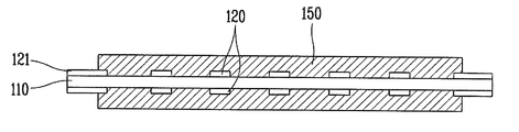
도 1은 본 발명의 일실시예에 관련된 인쇄회로기판(100)의 사시도이고, 도 2는 도 1에 도시된 절연부재(110)의 평면도이며, 도 3은 도 1의 Ⅲ-Ⅲ 라인을 따르는 인쇄회로기판(100)의 단면도이다.1 is a perspective view of a printed
본 발명에 관련된 인쇄회로기판(100)은 절연부재(110), 회로패턴(120, 도 3 참조) 및 지지부재(130)를 포함한다.The printed
절연부재(110)는 인쇄회로기판(100)의 외관을 형성하며, 인쇄회로기판(100)에 내구력을 제공하는 기초부재로서의 기능을 한다. 절연부재(110)는 페놀수지로 구성되거나, 유리섬유가 포함된 에폭시 등과 같은 물질로 구성될 수도 있다.The
본 실시예에 관련된 절연부재(110)는 인쇄회로기판(110)에 실장되는 전자소자들의 두께 증가에 따른 영향을 최소화하기 위해 130㎛ 이하의 박형으로 형성될 수 있다.The insulating
도 2를 참조하면, 절연부재(110)는 적어도 어느 일면에 형성되는 제1영역(111)과, 제1영역(111)의 가장자리에 형성되는 제2영역(112)을 구비한다. 본 실시예와 같이 절연부재(110)가 직사각형의 형태로 형성되는 경우, 제2영역(112)은 절연부재(110)의 테두리를 따라 형성되고, 제1영역(111)은 제2영역(112)의 내측에 형성될 수 있다.Referring to FIG. 2, the
제1영역(111)에는 회로패턴(120)이 형성되며, 회로패턴(120)은 도전성 재질, 예를 들어 구리 재질로 형성될 수 있다. 회로패턴(120)은 해당 회로의 설계에 따라 다양한 패턴을 가질 수 있다.The
제2영역(112)에는 절연부재(110)가 평면의 형태를 유지하도록 절연부재(110)를 지지하는 지지부재(130)가 구비된다. 지지부재(130)는 일정 폭을 갖는 밴드 형태로 형성될 수 있으며, 절연부재(110)의 제1영역(111)을 둘러싸는 형태로 형성될 수 있다.The
지지부재(130)는 금속재질(예를 들어, 구리)로 형성될 수 있으며, 회로패턴(120)과 동일한 재질로 형성되는 것도 가능하다.The
한편, 제2영역(112)에는 도전성 재질의 도전 패턴(121)이 형성될 수 있으며, 지지부재(130)는 도전 패턴(121)의 상면에 형성될 수 있다. 도전패턴(121)은 지지부재(130)가 전기 도금에 의해 형성되는 경우, 도전 패턴(121)에는 전기 도금을 위한 전류가 흐르게 된다. 또한 이와 동시에 도전패턴(121)이 구비됨으로써 지지부재(130)의 형성시 도전패턴(121)이 갖는 두께만큼 지지부재(130)의 두께를 줄일 수 있다. 도 3에서는 지지부재(130)가 도전패턴(121)의 상면에 형성된 것이 도시되어 있으나, 본 발명에 관련된 인쇄회로기판(100)은 도전패턴(121)이 생략되는 구성을 가질 수도 있다.Meanwhile, a
절연부재(110), 회로패턴(120), 및 지지부재(130)의 표면에는 이들을 덮는 보호층(140)이 더 구비될 수 있다. 보호층(140)은 이들 구성요소들이 물리적, 화학적으로 외부로부터 영향을 받는 것을 최소화한다. 보호층(140)은 불변성 화합물인 솔더 마스크 잉크(solder mask ink)를 절연부재(110), 회로패턴(120), 및 지지부재(130)에 코팅함으로써 형성될 수 있다.The
한편, 본 실시예에서는 절연부재(110)에 구비되는 구성들(회로패턴, 도전패턴, 지지부재, 보호층)이 절연부재(110)의 상면과 하면에 각각 구비되나, 이들 구성들은 절연부재(110)의 상면과 하면 중 어느 일면에만 구비되는 것도 가능하다.On the other hand, in the present embodiment, the components (circuit pattern, conductive pattern, support member, protective layer) provided in the
본 발명에 관련된 인쇄회로기판(100)은 절연부재(110)의 제2영역(112)에 지지부재(130)가 구비됨으로써 평면의 형태가 유지될 수 있게 된다. 이에 따라 인쇄회로기판(110)의 두께가 매우 얇더라도 인쇄회로기판(100)의 평면(회로패턴이 형성된 영역)에 수직한 방향으로 변형이 일어나는 것을 최소화할 수 있다. 이에 따라 컨베이어(conveyor)의 이동시 인쇄회로기판(100)이 변형되어 벨트의 안쪽으로 말려 들어가는 현상, 도금 공정 중에 도금 유동액에 의해 인쇄회로기판(100)이 찢어지는 현상, 절연잉크의 인쇄공정 중에 인쇄회로기판(100)이 스크린에 달라붙는 현상 등을 방지할 수 있다.In the printed
다음으로, 본 발명에 관련된 인쇄회로기판(100)의 제조방법에 대하여 살펴보기로 한다. 도 4a 내지 4f는 본 발명에 관련된 인쇄회로기판(100)의 제조공정을 순 차적으로 나타낸 도면들이다.Next, a manufacturing method of the printed
먼저, 도 4a에 도시된 바와 같이 절연부재(110)의 제1영역(111)에 도전성 재질의 회로패턴(120)이 형성된다. 회로패턴(120)은 전기 도금, 포토레지스트(photoresist)를 이용하는 방식 등 다양한 방식에 의해 형성될 수 있다. First, as shown in FIG. 4A, a
본 단계에서는 절연부재(110)의 제2영역(112)에 도전 패턴(121)이 형성될 수 있고, 도전패턴(121)은 회로패턴(120)과 동일한 방식으로 형성될 수 있다. 본 단계에서 도전 패턴(121)과 회로 패턴(120)은 동일한 재료로서 동시에 형성될 수 있다.In this step, the
다음으로, 도 4b와 같이 절연부재(110)의 일면에 기초부재(150)가 형성되며, 기초부재(150)로서 포토 레지스트 필름이 사용될 수 있다. 여기서, 포토레지스트는 얇은 막으로 만들어 빛을 쐬면 내약품성이 큰 경질막으로 변화하는 감광성 재료를 말한다.Next, as shown in FIG. 4B, the
포토레지스트 필름의 상면에 마스크가 위치되며, 포토레지스트 필름에 자외선이 조사되게 된다. 포토레지스트는 포지티브(positive) 또는 네거티브(negative) 포토 레지스트가 사용될 수 있으며, 포지티브 포토레지스트가 사용된 경우 포토 레지스트 중 제2영역(112)에 상응하는 영역이 자외선과 상호 반응하게 된다. The mask is positioned on the upper surface of the photoresist film, and the ultraviolet rays are irradiated onto the photoresist film. As the photoresist, a positive or negative photoresist may be used. When the positive photoresist is used, a region corresponding to the
포토레지스트를 현상시키면, 도 4c와 같이 포토레지스트 중 제2영역(112)에 상응하는 영역이 제거되게 된다. 그리고, 포토레지스트의 제거된 영역에 도 4d와 같이 지지부재(130)가 형성된다. 지지부재(130)의 재질로서 구리 등의 금속재질이 사용될 수 있고, 이는 전기 도금에 의해 형성될 수 있다. 여기서 절연부재(110)의 제2영역(112)에 형성된 도전패턴(121)에는 전기 도금을 위한 전류가 흐르게 된다. 지지부재(130)는 전기 도금 뿐만 아니라 인쇄 및 경화에 의하여 형성될 수도 있으며, 이 경우에는 제2영역(112)에 도전 패턴(121)을 형성시키는 공정이 생략될 수도 있다.When the photoresist is developed, a region corresponding to the
다음으로 절연부재(110)에 위치한 기초부재(150)가 제거되면, 도 4e와 같이 절연부재(110)에는 회로패턴(120), 도전패턴(121), 및 지지부재(130)만 남아 있게 된다. 기초부재(150)로서 포토레지스트가 사용된 경우, 포토레지스트는 에칭 용액을 이용하여 제거되거나, 물리적으로 박리시켜 제거될 수 있다.Next, when the
도 4f와 같이 절연부재(110), 회로패턴(120), 및 지지부재(130)의 표면에는 솔더 마스크 잉크가 코팅되어 보호층(140)이 형성될 수도 있다.As shown in FIG. 4F, a solder mask ink may be coated on surfaces of the insulating
이하에서는 본 발명에 관련된 인쇄회로기판 제조용 패널(200)에 대해 살펴보기로 한다. 도 5는 본 발명의 일실시예에 관련된 인쇄회로기판 제조용 패널(200)의 평면도이고, 도 6은 도 5의 Ⅵ-Ⅵ 라인을 따르는 인쇄회로기판 제조용 패널(200)의 단면도이다.Hereinafter, the printed circuit
인쇄회로기판 제조용 패널(200)은 복수의 인쇄회로기판(100)들이 배열되어 인쇄회로기판(100)들을 동시에 제조하기 위한 것으로서, 프레임(211), 인쇄회로기판(100), 및 지지부재(221)를 포함한다. The printed circuit
프레임(211)은 복수의 개소에 형성되는 제1영역(210)들과, 제1영역(210)들을 제외한 나머지 영역에 형성되는 제2영역(220)을 구비한다. 프레임(211)은 인쇄회로기판(100)의 절연부재(110)와 동일한 재질로 형성될 수 있다. 그리고, 프레임(211)은 본 실시예와 같이 절연부재(110)와 별개로 형성될 수도 있으나, 절연부재(110) 와 일체로 형성되는 것도 가능하다. 또한, 프레임(211)은 절연부재(110)와 동일한 두께로 형성될 수 있다.The
프레임(211)의 제1영역(210)들에는 복수의 인쇄회로기판(100)들이 각각 구비되며, 인쇄회로기판(100)들에 대한 설명은 앞선 설명에 갈음하기로 한다. 다만, 프레임(211)에 배열되는 인쇄회로기판(100)은 앞선 실시예에서의 구성 중 도전패턴(121), 지지부재(130)가 생략되는 구성도 가질 수도 있다. A plurality of printed
프레임(211)의 제2영역(220)에는 프레임(211)이 평면 형태를 유지하도록 프레임(211)을 지지하는 지지부재(221)가 구비되며, 지지부재(221)는 구리 등의 금속재질로 형성될 수 있다. 지지부재(221)는 앞서 설명한 인쇄회로기판(100)의 제조방법에서의 지지부재(130) 형성 방식과 동일한 방식으로 구현될 수 있다.The
인쇄회로기판(100)에 전자 소자가 실장되는 등의 공정이 완료되면, 인쇄회로기판 제조용 패널(200)에 배치된 인쇄회로기판(100)들이 프레임(211)으로부터 분리되게 되어 인쇄회로기판(100)의 모든 제조공정이 완료되게 된다.When the process of mounting the electronic device on the printed
상기와 같이 인쇄회로기판 제조용 패널(200)은 인쇄회로기판(100)이 배열된 제1영역(210)을 제외한 제2영역(220)에 지지부재(221)를 구비함으로써 프레임(211)의 두께가 매우 얇더라도 프레임(211)에 변형이 일어나는 것을 최소화하여 제조공정의 신뢰성을 향상시킬 수 있다.As described above, the
상기와 같이 설명된 인쇄회로기판의 제조과정은 상기 설명된 각 단계를 순차적으로 수행하여 제조되어야만 하는 것이 아니라 설계 사양에 따라 상기 각 공정의 단계가 선택적으로 혼용되어 수행될 수도 있다. 따라서, 상기 공정들이 혼용되어 수행되는 과정을 통해 제조될 수 있는 인쇄회로기판 및 인쇄회로기판 제조용 패널의 구성들 또한 본 발명의 기술적 사상의 범위 내에서 다양한 변형을 포함할 수 있다.The manufacturing process of the printed circuit board described above does not have to be manufactured by sequentially performing the above-described steps, but may be performed by selectively mixing the steps of each process according to design specifications. Accordingly, the configurations of the printed circuit board and the panel for manufacturing the printed circuit board, which may be manufactured through a process in which the above processes are mixed, may also include various modifications within the scope of the inventive concept.
도 1은 본 발명의 일실시예에 관련된 인쇄회로기판의 사시도.1 is a perspective view of a printed circuit board according to an embodiment of the present invention.
도 2는 도 1에 도시된 절연부재의 평면도.2 is a plan view of the insulating member shown in FIG.
도 3은 도 1의 Ⅲ-Ⅲ 라인을 따르는 인쇄회로기판의 단면도.3 is a cross-sectional view of the printed circuit board along the III-III line of FIG.
도 4a 내지 4f는 본 발명에 관련된 인쇄회로기판의 제조공정을 순차적으로 나타낸 도면들.4a to 4f are views sequentially showing a manufacturing process of a printed circuit board according to the present invention.
도 5는 본 발명의 일실시예에 관련된 인쇄회로기판 제조용 패널의 평면도.5 is a plan view of a panel for manufacturing a printed circuit board according to an embodiment of the present invention.
도 6은 도 5의 Ⅵ-Ⅵ 라인을 따르는 인쇄회로기판 제조용 패널의 단면도.6 is a cross-sectional view of a panel for manufacturing a printed circuit board along a VI-VI line of FIG. 5.
Claims (12)
Priority Applications (6)
| Application Number | Priority Date | Filing Date | Title |
|---|---|---|---|
| KR1020070123059A KR20090056077A (en) | 2007-11-29 | 2007-11-29 | Printed circuit board, method for manufacturing the same, and panel for manufacturing the same |
| TW097146120A TWI440407B (en) | 2007-11-29 | 2008-11-28 | Printed circuit board and method for manufacturing the same, and panel for manufacturing the printed circuit board |
| CN2008801236813A CN101919319A (en) | 2007-11-29 | 2008-12-01 | Printed circuit board and method for manufacturing the same, and panel for manufacturing the printed circuit board |
| JP2010535890A JP5426567B2 (en) | 2007-11-29 | 2008-12-01 | Printed circuit board, manufacturing method thereof, and panel for manufacturing printed circuit board |
| US12/745,667 US8426739B2 (en) | 2007-11-29 | 2008-12-01 | Printed circuit board and method for manufacturing the same, and panel for manufacturing the printed circuit board |
| PCT/KR2008/007088 WO2009069987A2 (en) | 2007-11-29 | 2008-12-01 | Printed circuit board and method for manufacturing the same, and panel for manufacturing the printed circuit board |
Applications Claiming Priority (1)
| Application Number | Priority Date | Filing Date | Title |
|---|---|---|---|
| KR1020070123059A KR20090056077A (en) | 2007-11-29 | 2007-11-29 | Printed circuit board, method for manufacturing the same, and panel for manufacturing the same |
Publications (1)
| Publication Number | Publication Date |
|---|---|
| KR20090056077A true KR20090056077A (en) | 2009-06-03 |
Family
ID=40679164
Family Applications (1)
| Application Number | Title | Priority Date | Filing Date |
|---|---|---|---|
| KR1020070123059A KR20090056077A (en) | 2007-11-29 | 2007-11-29 | Printed circuit board, method for manufacturing the same, and panel for manufacturing the same |
Country Status (6)
| Country | Link |
|---|---|
| US (1) | US8426739B2 (en) |
| JP (1) | JP5426567B2 (en) |
| KR (1) | KR20090056077A (en) |
| CN (1) | CN101919319A (en) |
| TW (1) | TWI440407B (en) |
| WO (1) | WO2009069987A2 (en) |
Families Citing this family (4)
| Publication number | Priority date | Publication date | Assignee | Title |
|---|---|---|---|---|
| TWI560454B (en) * | 2014-11-07 | 2016-12-01 | Primax Electronics Ltd | Testing base |
| US10477671B2 (en) * | 2015-09-30 | 2019-11-12 | Sekisui Chemical Co., Ltd. | Laminated body |
| JP7065617B2 (en) * | 2018-01-12 | 2022-05-12 | 新光電気工業株式会社 | Substrate with support and its manufacturing method |
| CN109275272A (en) * | 2018-11-27 | 2019-01-25 | 景旺电子科技(龙川)有限公司 | A kind of thin pcb board processing method |
Family Cites Families (13)
| Publication number | Priority date | Publication date | Assignee | Title |
|---|---|---|---|---|
| JPS5667982A (en) | 1979-11-07 | 1981-06-08 | Tdk Electronics Co Ltd | Printed circuit board and method of manufacturing same |
| JPS62124571U (en) * | 1986-01-31 | 1987-08-07 | ||
| JPH0680872B2 (en) | 1988-11-29 | 1994-10-12 | 日本電気株式会社 | Flexible printed circuit board sheet |
| JP3437369B2 (en) * | 1996-03-19 | 2003-08-18 | 松下電器産業株式会社 | Chip carrier and semiconductor device using the same |
| US6020221A (en) * | 1996-12-12 | 2000-02-01 | Lsi Logic Corporation | Process for manufacturing a semiconductor device having a stiffener member |
| JPH11214806A (en) | 1998-01-23 | 1999-08-06 | Nec Saitama Ltd | Printed board reinforcing structure |
| JP2000164997A (en) | 1998-11-27 | 2000-06-16 | Denso Corp | Printed board and method of mounting parts thereon |
| JP3635219B2 (en) * | 1999-03-11 | 2005-04-06 | 新光電気工業株式会社 | Multilayer substrate for semiconductor device and manufacturing method thereof |
| US6204559B1 (en) * | 1999-11-22 | 2001-03-20 | Advanced Semiconductor Engineering, Inc. | Ball grid assembly type semiconductor package having improved chip edge support to prevent chip cracking |
| JP2003209366A (en) * | 2002-01-15 | 2003-07-25 | Sony Corp | Flexible multilayer wiring board and manufacturing method therefor |
| JP2005531160A (en) * | 2002-06-27 | 2005-10-13 | ピーピージー インダストリーズ オハイオ, インコーポレイテッド | Single or multi-layer printed circuit board having recessed or expanded breakaway tabs and method for manufacturing the same |
| KR100992637B1 (en) | 2003-07-24 | 2010-11-05 | 엘지이노텍 주식회사 | Basic material for PCB and PCB making method using the same |
| KR100736633B1 (en) | 2005-12-19 | 2007-07-06 | 삼성전기주식회사 | Reinforcement substrate and manufacturing method |
-
2007
- 2007-11-29 KR KR1020070123059A patent/KR20090056077A/en active Search and Examination
-
2008
- 2008-11-28 TW TW097146120A patent/TWI440407B/en active
- 2008-12-01 WO PCT/KR2008/007088 patent/WO2009069987A2/en active Application Filing
- 2008-12-01 CN CN2008801236813A patent/CN101919319A/en active Pending
- 2008-12-01 JP JP2010535890A patent/JP5426567B2/en active Active
- 2008-12-01 US US12/745,667 patent/US8426739B2/en active Active
Also Published As
| Publication number | Publication date |
|---|---|
| US20110036618A1 (en) | 2011-02-17 |
| TWI440407B (en) | 2014-06-01 |
| TW200934310A (en) | 2009-08-01 |
| WO2009069987A2 (en) | 2009-06-04 |
| CN101919319A (en) | 2010-12-15 |
| US8426739B2 (en) | 2013-04-23 |
| JP2011505690A (en) | 2011-02-24 |
| WO2009069987A3 (en) | 2009-08-20 |
| JP5426567B2 (en) | 2014-02-26 |
Similar Documents
| Publication | Publication Date | Title |
|---|---|---|
| CN105430877B (en) | The preparation method of flexible PCB, terminal and flexible PCB | |
| US7799603B2 (en) | Method for mounting electronic component on printed circuit board | |
| EP1971194A2 (en) | Wiring substrate and manufacturing method thereof | |
| US8067696B2 (en) | Printed circuit board and method for manufacturing same | |
| KR20090056077A (en) | Printed circuit board, method for manufacturing the same, and panel for manufacturing the same | |
| CN100367490C (en) | Diaphragm bearing belt for mounting electronic device and its mfg. method | |
| CN112074098A (en) | Printed circuit board | |
| KR101847163B1 (en) | Printed circuit board and method of manufacturing the same | |
| KR20050061343A (en) | Wiring circuit board | |
| KR20130041645A (en) | Printed circuit board | |
| CN216217750U (en) | Electroplating type stepped welding pad PCB | |
| US20130240254A1 (en) | Printed circuit board and method for manufacturing printed circuit board | |
| KR101317952B1 (en) | Manufacturing method of led module including chip on board dam using transfer mold and led module thereby | |
| KR20070062079A (en) | Printed circuit board having align mark and manufacturing method thereof | |
| KR20150107141A (en) | The printed circuit board and the method for manufacturing the same | |
| KR101022869B1 (en) | A printed circuit board and method of manufacturing method of the printed circuit board for image sensor module | |
| KR102096083B1 (en) | Stiffening plate panel for printed circuit board and method for manufacturing the same | |
| US20090266587A1 (en) | Flexible printed circuit board and method of forming fine pitch therein | |
| CN113316318A (en) | Electroplating type stepped welding disc PCB and manufacturing technology | |
| JP4087741B2 (en) | Tape carrier, semiconductor module, and method of manufacturing semiconductor module | |
| CN113811074A (en) | Printed circuit board manufacturing method, golden finger protection method and protection structure | |
| CN113939112A (en) | Circuit board manufacturing method and circuit board | |
| JP2000309151A (en) | Method for printing pastelike substance | |
| KR20150115346A (en) | The printed circuit board and the method for manufacturing the same | |
| KR101043475B1 (en) | Jig for multilayer ceramic board and manufacturing method of multilayer ceramic board using the same |
Legal Events
| Date | Code | Title | Description |
|---|---|---|---|
| N231 | Notification of change of applicant | ||
| A201 | Request for examination | ||
| E902 | Notification of reason for refusal | ||
| AMND | Amendment | ||
| E601 | Decision to refuse application | ||
| AMND | Amendment | ||
| J121 | Written withdrawal of request for trial | ||
| J201 | Request for trial against refusal decision | ||
| E801 | Decision on dismissal of amendment | ||
| B601 | Maintenance of original decision after re-examination before a trial | ||
| J301 | Trial decision |
Free format text: TRIAL DECISION FOR APPEAL AGAINST DECISION TO DECLINE REFUSAL REQUESTED 20140430 Effective date: 20141229 Free format text: TRIAL NUMBER: 2014101002632; TRIAL DECISION FOR APPEAL AGAINST DECISION TO DECLINE REFUSAL REQUESTED 20140430 Effective date: 20141229 |