KR20090026741A - Electro-optical device, method of manufacturing the same, and electronic apparatus - Google Patents
Electro-optical device, method of manufacturing the same, and electronic apparatus Download PDFInfo
- Publication number
- KR20090026741A KR20090026741A KR1020080089260A KR20080089260A KR20090026741A KR 20090026741 A KR20090026741 A KR 20090026741A KR 1020080089260 A KR1020080089260 A KR 1020080089260A KR 20080089260 A KR20080089260 A KR 20080089260A KR 20090026741 A KR20090026741 A KR 20090026741A
- Authority
- KR
- South Korea
- Prior art keywords
- region
- insulating film
- data line
- pixel electrode
- drain region
- Prior art date
Links
- 238000004519 manufacturing process Methods 0.000 title abstract description 29
- 239000000758 substrate Substances 0.000 claims abstract description 94
- 239000004065 semiconductor Substances 0.000 claims abstract description 74
- 150000004767 nitrides Chemical class 0.000 claims description 38
- 238000000034 method Methods 0.000 claims description 31
- NBIIXXVUZAFLBC-UHFFFAOYSA-N Phosphoric acid Chemical compound OP(O)(O)=O NBIIXXVUZAFLBC-UHFFFAOYSA-N 0.000 claims description 24
- 150000002500 ions Chemical class 0.000 claims description 15
- 230000008569 process Effects 0.000 claims description 15
- 229910000147 aluminium phosphate Inorganic materials 0.000 claims description 12
- 238000010306 acid treatment Methods 0.000 claims description 8
- 238000000059 patterning Methods 0.000 claims description 7
- 239000010408 film Substances 0.000 description 272
- 239000010410 layer Substances 0.000 description 117
- 239000004973 liquid crystal related substance Substances 0.000 description 54
- 239000003990 capacitor Substances 0.000 description 37
- 230000003287 optical effect Effects 0.000 description 25
- 230000000694 effects Effects 0.000 description 17
- 230000001443 photoexcitation Effects 0.000 description 17
- 238000003860 storage Methods 0.000 description 15
- 230000005284 excitation Effects 0.000 description 13
- 229910052751 metal Inorganic materials 0.000 description 12
- 239000002184 metal Substances 0.000 description 12
- 238000010586 diagram Methods 0.000 description 10
- 239000012535 impurity Substances 0.000 description 10
- VYPSYNLAJGMNEJ-UHFFFAOYSA-N Silicium dioxide Chemical compound O=[Si]=O VYPSYNLAJGMNEJ-UHFFFAOYSA-N 0.000 description 9
- 239000011159 matrix material Substances 0.000 description 9
- 239000011229 interlayer Substances 0.000 description 8
- 230000007257 malfunction Effects 0.000 description 8
- 229910021420 polycrystalline silicon Inorganic materials 0.000 description 8
- 229920005591 polysilicon Polymers 0.000 description 8
- 238000005530 etching Methods 0.000 description 7
- 239000010409 thin film Substances 0.000 description 7
- 230000007423 decrease Effects 0.000 description 6
- 230000007547 defect Effects 0.000 description 6
- 229910052581 Si3N4 Inorganic materials 0.000 description 5
- 230000008859 change Effects 0.000 description 5
- 239000004020 conductor Substances 0.000 description 5
- 238000005468 ion implantation Methods 0.000 description 5
- 239000000463 material Substances 0.000 description 5
- HQVNEWCFYHHQES-UHFFFAOYSA-N silicon nitride Chemical compound N12[Si]34N5[Si]62N3[Si]51N64 HQVNEWCFYHHQES-UHFFFAOYSA-N 0.000 description 5
- 238000012360 testing method Methods 0.000 description 5
- 238000005229 chemical vapour deposition Methods 0.000 description 4
- 230000005684 electric field Effects 0.000 description 4
- 230000002093 peripheral effect Effects 0.000 description 4
- 239000005368 silicate glass Substances 0.000 description 4
- 229910052814 silicon oxide Inorganic materials 0.000 description 4
- 239000010936 titanium Substances 0.000 description 4
- 229910004298 SiO 2 Inorganic materials 0.000 description 3
- 229910045601 alloy Inorganic materials 0.000 description 3
- 239000000956 alloy Substances 0.000 description 3
- 229910052782 aluminium Inorganic materials 0.000 description 3
- XAGFODPZIPBFFR-UHFFFAOYSA-N aluminium Chemical compound [Al] XAGFODPZIPBFFR-UHFFFAOYSA-N 0.000 description 3
- 239000011521 glass Substances 0.000 description 3
- 230000007246 mechanism Effects 0.000 description 3
- KDLHZDBZIXYQEI-UHFFFAOYSA-N palladium Substances [Pd] KDLHZDBZIXYQEI-UHFFFAOYSA-N 0.000 description 3
- 230000001681 protective effect Effects 0.000 description 3
- 230000001105 regulatory effect Effects 0.000 description 3
- 239000003566 sealing material Substances 0.000 description 3
- 235000012239 silicon dioxide Nutrition 0.000 description 3
- 239000002356 single layer Substances 0.000 description 3
- ZOXJGFHDIHLPTG-UHFFFAOYSA-N Boron Chemical compound [B] ZOXJGFHDIHLPTG-UHFFFAOYSA-N 0.000 description 2
- BQCADISMDOOEFD-UHFFFAOYSA-N Silver Chemical compound [Ag] BQCADISMDOOEFD-UHFFFAOYSA-N 0.000 description 2
- BOTDANWDWHJENH-UHFFFAOYSA-N Tetraethyl orthosilicate Chemical compound CCO[Si](OCC)(OCC)OCC BOTDANWDWHJENH-UHFFFAOYSA-N 0.000 description 2
- RTAQQCXQSZGOHL-UHFFFAOYSA-N Titanium Chemical compound [Ti] RTAQQCXQSZGOHL-UHFFFAOYSA-N 0.000 description 2
- NRTOMJZYCJJWKI-UHFFFAOYSA-N Titanium nitride Chemical compound [Ti]#N NRTOMJZYCJJWKI-UHFFFAOYSA-N 0.000 description 2
- 230000000903 blocking effect Effects 0.000 description 2
- 229910052796 boron Inorganic materials 0.000 description 2
- 239000000969 carrier Substances 0.000 description 2
- 239000011651 chromium Substances 0.000 description 2
- 238000000151 deposition Methods 0.000 description 2
- 238000010438 heat treatment Methods 0.000 description 2
- 238000002513 implantation Methods 0.000 description 2
- 238000009413 insulation Methods 0.000 description 2
- 230000001678 irradiating effect Effects 0.000 description 2
- 230000031700 light absorption Effects 0.000 description 2
- 230000014759 maintenance of location Effects 0.000 description 2
- 238000002844 melting Methods 0.000 description 2
- 230000008018 melting Effects 0.000 description 2
- 230000004048 modification Effects 0.000 description 2
- 238000012986 modification Methods 0.000 description 2
- 239000011347 resin Substances 0.000 description 2
- 229920005989 resin Polymers 0.000 description 2
- 238000005070 sampling Methods 0.000 description 2
- 229910021332 silicide Inorganic materials 0.000 description 2
- FVBUAEGBCNSCDD-UHFFFAOYSA-N silicide(4-) Chemical compound [Si-4] FVBUAEGBCNSCDD-UHFFFAOYSA-N 0.000 description 2
- 239000000377 silicon dioxide Substances 0.000 description 2
- 229910052709 silver Inorganic materials 0.000 description 2
- 239000004332 silver Substances 0.000 description 2
- 229910052719 titanium Inorganic materials 0.000 description 2
- 238000002834 transmittance Methods 0.000 description 2
- WFKWXMTUELFFGS-UHFFFAOYSA-N tungsten Chemical compound [W] WFKWXMTUELFFGS-UHFFFAOYSA-N 0.000 description 2
- 229910052721 tungsten Inorganic materials 0.000 description 2
- 239000010937 tungsten Substances 0.000 description 2
- 241001270131 Agaricus moelleri Species 0.000 description 1
- 229910018182 Al—Cu Inorganic materials 0.000 description 1
- VYZAMTAEIAYCRO-UHFFFAOYSA-N Chromium Chemical compound [Cr] VYZAMTAEIAYCRO-UHFFFAOYSA-N 0.000 description 1
- ZOKXTWBITQBERF-UHFFFAOYSA-N Molybdenum Chemical compound [Mo] ZOKXTWBITQBERF-UHFFFAOYSA-N 0.000 description 1
- 239000004988 Nematic liquid crystal Substances 0.000 description 1
- 229910019142 PO4 Inorganic materials 0.000 description 1
- OAICVXFJPJFONN-UHFFFAOYSA-N Phosphorus Chemical compound [P] OAICVXFJPJFONN-UHFFFAOYSA-N 0.000 description 1
- 229910018594 Si-Cu Inorganic materials 0.000 description 1
- XUIMIQQOPSSXEZ-UHFFFAOYSA-N Silicon Chemical compound [Si] XUIMIQQOPSSXEZ-UHFFFAOYSA-N 0.000 description 1
- 229910008465 Si—Cu Inorganic materials 0.000 description 1
- 229910021417 amorphous silicon Inorganic materials 0.000 description 1
- 239000011324 bead Substances 0.000 description 1
- 229910052804 chromium Inorganic materials 0.000 description 1
- 238000004140 cleaning Methods 0.000 description 1
- 239000003086 colorant Substances 0.000 description 1
- 238000011109 contamination Methods 0.000 description 1
- 230000003247 decreasing effect Effects 0.000 description 1
- 230000006866 deterioration Effects 0.000 description 1
- KUGSJJNCCNSRMM-UHFFFAOYSA-N ethoxyboronic acid Chemical compound CCOB(O)O KUGSJJNCCNSRMM-UHFFFAOYSA-N 0.000 description 1
- 239000003365 glass fiber Substances 0.000 description 1
- 229910052736 halogen Inorganic materials 0.000 description 1
- 150000002367 halogens Chemical class 0.000 description 1
- 230000006872 improvement Effects 0.000 description 1
- AMGQUBHHOARCQH-UHFFFAOYSA-N indium;oxotin Chemical compound [In].[Sn]=O AMGQUBHHOARCQH-UHFFFAOYSA-N 0.000 description 1
- 238000007689 inspection Methods 0.000 description 1
- 238000012423 maintenance Methods 0.000 description 1
- 238000005259 measurement Methods 0.000 description 1
- 239000007769 metal material Substances 0.000 description 1
- 229910052750 molybdenum Inorganic materials 0.000 description 1
- 239000011733 molybdenum Substances 0.000 description 1
- 239000000382 optic material Substances 0.000 description 1
- 230000003647 oxidation Effects 0.000 description 1
- 238000007254 oxidation reaction Methods 0.000 description 1
- 229910052763 palladium Inorganic materials 0.000 description 1
- 239000010452 phosphate Substances 0.000 description 1
- 229910052698 phosphorus Inorganic materials 0.000 description 1
- 239000011574 phosphorus Substances 0.000 description 1
- 238000005268 plasma chemical vapour deposition Methods 0.000 description 1
- 238000005498 polishing Methods 0.000 description 1
- 238000012545 processing Methods 0.000 description 1
- 230000000644 propagated effect Effects 0.000 description 1
- 239000010453 quartz Substances 0.000 description 1
- 230000009467 reduction Effects 0.000 description 1
- 229910052710 silicon Inorganic materials 0.000 description 1
- 239000010703 silicon Substances 0.000 description 1
- 229910052715 tantalum Inorganic materials 0.000 description 1
- GUVRBAGPIYLISA-UHFFFAOYSA-N tantalum atom Chemical compound [Ta] GUVRBAGPIYLISA-UHFFFAOYSA-N 0.000 description 1
- 125000003698 tetramethyl group Chemical group [H]C([H])([H])* 0.000 description 1
- 229920001187 thermosetting polymer Polymers 0.000 description 1
- 239000012780 transparent material Substances 0.000 description 1
Images


Classifications
-
- G—PHYSICS
- G02—OPTICS
- G02F—OPTICAL DEVICES OR ARRANGEMENTS FOR THE CONTROL OF LIGHT BY MODIFICATION OF THE OPTICAL PROPERTIES OF THE MEDIA OF THE ELEMENTS INVOLVED THEREIN; NON-LINEAR OPTICS; FREQUENCY-CHANGING OF LIGHT; OPTICAL LOGIC ELEMENTS; OPTICAL ANALOGUE/DIGITAL CONVERTERS
- G02F1/00—Devices or arrangements for the control of the intensity, colour, phase, polarisation or direction of light arriving from an independent light source, e.g. switching, gating or modulating; Non-linear optics
- G02F1/01—Devices or arrangements for the control of the intensity, colour, phase, polarisation or direction of light arriving from an independent light source, e.g. switching, gating or modulating; Non-linear optics for the control of the intensity, phase, polarisation or colour
- G02F1/13—Devices or arrangements for the control of the intensity, colour, phase, polarisation or direction of light arriving from an independent light source, e.g. switching, gating or modulating; Non-linear optics for the control of the intensity, phase, polarisation or colour based on liquid crystals, e.g. single liquid crystal display cells
- G02F1/133—Constructional arrangements; Operation of liquid crystal cells; Circuit arrangements
- G02F1/136—Liquid crystal cells structurally associated with a semi-conducting layer or substrate, e.g. cells forming part of an integrated circuit
-
- H—ELECTRICITY
- H01—ELECTRIC ELEMENTS
- H01L—SEMICONDUCTOR DEVICES NOT COVERED BY CLASS H10
- H01L29/00—Semiconductor devices adapted for rectifying, amplifying, oscillating or switching, or capacitors or resistors with at least one potential-jump barrier or surface barrier, e.g. PN junction depletion layer or carrier concentration layer; Details of semiconductor bodies or of electrodes thereof ; Multistep manufacturing processes therefor
- H01L29/40—Electrodes ; Multistep manufacturing processes therefor
- H01L29/41—Electrodes ; Multistep manufacturing processes therefor characterised by their shape, relative sizes or dispositions
- H01L29/423—Electrodes ; Multistep manufacturing processes therefor characterised by their shape, relative sizes or dispositions not carrying the current to be rectified, amplified or switched
- H01L29/42312—Gate electrodes for field effect devices
- H01L29/42316—Gate electrodes for field effect devices for field-effect transistors
- H01L29/4232—Gate electrodes for field effect devices for field-effect transistors with insulated gate
- H01L29/42384—Gate electrodes for field effect devices for field-effect transistors with insulated gate for thin film field effect transistors, e.g. characterised by the thickness or the shape of the insulator or the dimensions, the shape or the lay-out of the conductor
-
- G—PHYSICS
- G02—OPTICS
- G02F—OPTICAL DEVICES OR ARRANGEMENTS FOR THE CONTROL OF LIGHT BY MODIFICATION OF THE OPTICAL PROPERTIES OF THE MEDIA OF THE ELEMENTS INVOLVED THEREIN; NON-LINEAR OPTICS; FREQUENCY-CHANGING OF LIGHT; OPTICAL LOGIC ELEMENTS; OPTICAL ANALOGUE/DIGITAL CONVERTERS
- G02F1/00—Devices or arrangements for the control of the intensity, colour, phase, polarisation or direction of light arriving from an independent light source, e.g. switching, gating or modulating; Non-linear optics
- G02F1/01—Devices or arrangements for the control of the intensity, colour, phase, polarisation or direction of light arriving from an independent light source, e.g. switching, gating or modulating; Non-linear optics for the control of the intensity, phase, polarisation or colour
- G02F1/13—Devices or arrangements for the control of the intensity, colour, phase, polarisation or direction of light arriving from an independent light source, e.g. switching, gating or modulating; Non-linear optics for the control of the intensity, phase, polarisation or colour based on liquid crystals, e.g. single liquid crystal display cells
- G02F1/133—Constructional arrangements; Operation of liquid crystal cells; Circuit arrangements
- G02F1/1333—Constructional arrangements; Manufacturing methods
- G02F1/1335—Structural association of cells with optical devices, e.g. polarisers or reflectors
-
- G—PHYSICS
- G02—OPTICS
- G02F—OPTICAL DEVICES OR ARRANGEMENTS FOR THE CONTROL OF LIGHT BY MODIFICATION OF THE OPTICAL PROPERTIES OF THE MEDIA OF THE ELEMENTS INVOLVED THEREIN; NON-LINEAR OPTICS; FREQUENCY-CHANGING OF LIGHT; OPTICAL LOGIC ELEMENTS; OPTICAL ANALOGUE/DIGITAL CONVERTERS
- G02F1/00—Devices or arrangements for the control of the intensity, colour, phase, polarisation or direction of light arriving from an independent light source, e.g. switching, gating or modulating; Non-linear optics
- G02F1/01—Devices or arrangements for the control of the intensity, colour, phase, polarisation or direction of light arriving from an independent light source, e.g. switching, gating or modulating; Non-linear optics for the control of the intensity, phase, polarisation or colour
- G02F1/13—Devices or arrangements for the control of the intensity, colour, phase, polarisation or direction of light arriving from an independent light source, e.g. switching, gating or modulating; Non-linear optics for the control of the intensity, phase, polarisation or colour based on liquid crystals, e.g. single liquid crystal display cells
- G02F1/133—Constructional arrangements; Operation of liquid crystal cells; Circuit arrangements
- G02F1/136—Liquid crystal cells structurally associated with a semi-conducting layer or substrate, e.g. cells forming part of an integrated circuit
- G02F1/1362—Active matrix addressed cells
- G02F1/136209—Light shielding layers, e.g. black matrix, incorporated in the active matrix substrate, e.g. structurally associated with the switching element
-
- G—PHYSICS
- G02—OPTICS
- G02F—OPTICAL DEVICES OR ARRANGEMENTS FOR THE CONTROL OF LIGHT BY MODIFICATION OF THE OPTICAL PROPERTIES OF THE MEDIA OF THE ELEMENTS INVOLVED THEREIN; NON-LINEAR OPTICS; FREQUENCY-CHANGING OF LIGHT; OPTICAL LOGIC ELEMENTS; OPTICAL ANALOGUE/DIGITAL CONVERTERS
- G02F1/00—Devices or arrangements for the control of the intensity, colour, phase, polarisation or direction of light arriving from an independent light source, e.g. switching, gating or modulating; Non-linear optics
- G02F1/01—Devices or arrangements for the control of the intensity, colour, phase, polarisation or direction of light arriving from an independent light source, e.g. switching, gating or modulating; Non-linear optics for the control of the intensity, phase, polarisation or colour
- G02F1/13—Devices or arrangements for the control of the intensity, colour, phase, polarisation or direction of light arriving from an independent light source, e.g. switching, gating or modulating; Non-linear optics for the control of the intensity, phase, polarisation or colour based on liquid crystals, e.g. single liquid crystal display cells
- G02F1/133—Constructional arrangements; Operation of liquid crystal cells; Circuit arrangements
- G02F1/136—Liquid crystal cells structurally associated with a semi-conducting layer or substrate, e.g. cells forming part of an integrated circuit
- G02F1/1362—Active matrix addressed cells
- G02F1/136213—Storage capacitors associated with the pixel electrode
-
- H—ELECTRICITY
- H01—ELECTRIC ELEMENTS
- H01L—SEMICONDUCTOR DEVICES NOT COVERED BY CLASS H10
- H01L27/00—Devices consisting of a plurality of semiconductor or other solid-state components formed in or on a common substrate
- H01L27/02—Devices consisting of a plurality of semiconductor or other solid-state components formed in or on a common substrate including semiconductor components specially adapted for rectifying, oscillating, amplifying or switching and having at least one potential-jump barrier or surface barrier; including integrated passive circuit elements with at least one potential-jump barrier or surface barrier
- H01L27/12—Devices consisting of a plurality of semiconductor or other solid-state components formed in or on a common substrate including semiconductor components specially adapted for rectifying, oscillating, amplifying or switching and having at least one potential-jump barrier or surface barrier; including integrated passive circuit elements with at least one potential-jump barrier or surface barrier the substrate being other than a semiconductor body, e.g. an insulating body
- H01L27/1214—Devices consisting of a plurality of semiconductor or other solid-state components formed in or on a common substrate including semiconductor components specially adapted for rectifying, oscillating, amplifying or switching and having at least one potential-jump barrier or surface barrier; including integrated passive circuit elements with at least one potential-jump barrier or surface barrier the substrate being other than a semiconductor body, e.g. an insulating body comprising a plurality of TFTs formed on a non-semiconducting substrate, e.g. driving circuits for AMLCDs
- H01L27/124—Devices consisting of a plurality of semiconductor or other solid-state components formed in or on a common substrate including semiconductor components specially adapted for rectifying, oscillating, amplifying or switching and having at least one potential-jump barrier or surface barrier; including integrated passive circuit elements with at least one potential-jump barrier or surface barrier the substrate being other than a semiconductor body, e.g. an insulating body comprising a plurality of TFTs formed on a non-semiconducting substrate, e.g. driving circuits for AMLCDs with a particular composition, shape or layout of the wiring layers specially adapted to the circuit arrangement, e.g. scanning lines in LCD pixel circuits
-
- H—ELECTRICITY
- H01—ELECTRIC ELEMENTS
- H01L—SEMICONDUCTOR DEVICES NOT COVERED BY CLASS H10
- H01L29/00—Semiconductor devices adapted for rectifying, amplifying, oscillating or switching, or capacitors or resistors with at least one potential-jump barrier or surface barrier, e.g. PN junction depletion layer or carrier concentration layer; Details of semiconductor bodies or of electrodes thereof ; Multistep manufacturing processes therefor
- H01L29/66—Types of semiconductor device ; Multistep manufacturing processes therefor
- H01L29/68—Types of semiconductor device ; Multistep manufacturing processes therefor controllable by only the electric current supplied, or only the electric potential applied, to an electrode which does not carry the current to be rectified, amplified or switched
- H01L29/76—Unipolar devices, e.g. field effect transistors
- H01L29/772—Field effect transistors
- H01L29/78—Field effect transistors with field effect produced by an insulated gate
- H01L29/786—Thin film transistors, i.e. transistors with a channel being at least partly a thin film
- H01L29/78606—Thin film transistors, i.e. transistors with a channel being at least partly a thin film with supplementary region or layer in the thin film or in the insulated bulk substrate supporting it for controlling or increasing the safety of the device
- H01L29/78618—Thin film transistors, i.e. transistors with a channel being at least partly a thin film with supplementary region or layer in the thin film or in the insulated bulk substrate supporting it for controlling or increasing the safety of the device characterised by the drain or the source properties, e.g. the doping structure, the composition, the sectional shape or the contact structure
- H01L29/78621—Thin film transistors, i.e. transistors with a channel being at least partly a thin film with supplementary region or layer in the thin film or in the insulated bulk substrate supporting it for controlling or increasing the safety of the device characterised by the drain or the source properties, e.g. the doping structure, the composition, the sectional shape or the contact structure with LDD structure or an extension or an offset region or characterised by the doping profile
-
- H—ELECTRICITY
- H01—ELECTRIC ELEMENTS
- H01L—SEMICONDUCTOR DEVICES NOT COVERED BY CLASS H10
- H01L29/00—Semiconductor devices adapted for rectifying, amplifying, oscillating or switching, or capacitors or resistors with at least one potential-jump barrier or surface barrier, e.g. PN junction depletion layer or carrier concentration layer; Details of semiconductor bodies or of electrodes thereof ; Multistep manufacturing processes therefor
- H01L29/66—Types of semiconductor device ; Multistep manufacturing processes therefor
- H01L29/68—Types of semiconductor device ; Multistep manufacturing processes therefor controllable by only the electric current supplied, or only the electric potential applied, to an electrode which does not carry the current to be rectified, amplified or switched
- H01L29/76—Unipolar devices, e.g. field effect transistors
- H01L29/772—Field effect transistors
- H01L29/78—Field effect transistors with field effect produced by an insulated gate
- H01L29/786—Thin film transistors, i.e. transistors with a channel being at least partly a thin film
- H01L29/78606—Thin film transistors, i.e. transistors with a channel being at least partly a thin film with supplementary region or layer in the thin film or in the insulated bulk substrate supporting it for controlling or increasing the safety of the device
- H01L29/78633—Thin film transistors, i.e. transistors with a channel being at least partly a thin film with supplementary region or layer in the thin film or in the insulated bulk substrate supporting it for controlling or increasing the safety of the device with a light shield
-
- G—PHYSICS
- G02—OPTICS
- G02F—OPTICAL DEVICES OR ARRANGEMENTS FOR THE CONTROL OF LIGHT BY MODIFICATION OF THE OPTICAL PROPERTIES OF THE MEDIA OF THE ELEMENTS INVOLVED THEREIN; NON-LINEAR OPTICS; FREQUENCY-CHANGING OF LIGHT; OPTICAL LOGIC ELEMENTS; OPTICAL ANALOGUE/DIGITAL CONVERTERS
- G02F1/00—Devices or arrangements for the control of the intensity, colour, phase, polarisation or direction of light arriving from an independent light source, e.g. switching, gating or modulating; Non-linear optics
- G02F1/01—Devices or arrangements for the control of the intensity, colour, phase, polarisation or direction of light arriving from an independent light source, e.g. switching, gating or modulating; Non-linear optics for the control of the intensity, phase, polarisation or colour
- G02F1/13—Devices or arrangements for the control of the intensity, colour, phase, polarisation or direction of light arriving from an independent light source, e.g. switching, gating or modulating; Non-linear optics for the control of the intensity, phase, polarisation or colour based on liquid crystals, e.g. single liquid crystal display cells
- G02F1/133—Constructional arrangements; Operation of liquid crystal cells; Circuit arrangements
- G02F1/136—Liquid crystal cells structurally associated with a semi-conducting layer or substrate, e.g. cells forming part of an integrated circuit
- G02F1/1362—Active matrix addressed cells
- G02F1/136286—Wiring, e.g. gate line, drain line
Abstract
Description
본 발명은 예를 들어 액정 장치 등의 전기 광학 장치, 및 그 전기 광학 장치의 제조 방법, 그리고 그 전기 광학 장치를 구비한, 예를 들어 액정 프로젝터 등의 전자 기기의 기술 분야에 관한 것이다. TECHNICAL FIELD This invention relates to the technical field of the electro-optical device, such as a liquid crystal device, the manufacturing method of this electro-optical device, and electronic equipment, such as a liquid crystal projector, provided with this electro-optical device, for example.
이러한 종류의 전기 광학 장치의 일례인 액정 장치는 직시형 디스플레이뿐만 아니라, 예를 들어 투사형 표시 장치의 광변조 수단 (라이트 밸브) 으로서도 다용되고 있다. 특히 투사형 표시 장치의 경우, 광원으로부터의 강한 광이 액정 라이트 밸브에 입사되기 때문에, 이 광에 의해 액정 라이트 밸브 내의 박막 트랜지스터 (TFT : Thin Film Transistor) 가 리크 전류의 증대나 오동작 등을 일으키지 않도록, 입사광을 차단하는 차광 수단으로서의 차광막이 액정 라이트 밸브에 내장되어 있다. The liquid crystal device which is an example of this kind of electro-optical device is used not only as a direct-view display but also as a light modulation means (light valve) of a projection display device, for example. In particular, in the case of a projection display device, since strong light from a light source is incident on the liquid crystal light valve, the thin film transistor (TFT) in the liquid crystal light valve does not cause leakage current to increase or malfunction due to the light. A light shielding film as light shielding means for blocking incident light is incorporated in the liquid crystal light valve.
이러한 차광 수단 또는 차광막에 대하여, 예를 들어 특허 문헌 1 은 TFT 의 채널 영역에서 게이트 전극으로서 기능하는 주사선에 의해 차광하는 기술을 개시하고 있다. 특허 문헌 2 에 의하면, 채널 영역 상에 형성된 복수의 차광막과, 내 면 반사광을 흡수하는 층을 형성함으로써 TFT 의 채널 영역에 도달하는 광을 저감시키고 있다. 특허 문헌 3 은 TFT 의 바람직한 동작의 확보 및 주사선의 협소화를 가능하게 하면서, TFT 의 채널 영역에 입사되는 입사광을 최대한 저감시키는 기술을 개시하고 있다. For example,
[특허 문헌 1] 일본 공개특허공보 2004-4722호[Patent Document 1] Japanese Unexamined Patent Publication No. 2004-4722
[특허 문헌 2] 일본 특허공보 제3731447호[Patent Document 2] Japanese Patent Publication No. 3731447
[특허 문헌 3] 일본 공개특허공보 2003-262888호[Patent Document 3] Japanese Unexamined Patent Publication No. 2003-262888
그러나, 상기 서술한 바와 같은 차광막에 의해 TFT 를 차광하는 경우, 차광막과 TFT 를 구성하는 반도체층 사이는 3 차원적으로 보아, 예를 들어 절연막 등을 개재시켜 이간되어 있어, 차광막의 옆에서 비스듬하게 입사되는 입사광이 TFT 를 구성하는 반도체층에 도달하여, TFT 에 있어서의 광리크 전류가 발생할 우려가 있다. 이러한 TFT 에 있어서의 광리크 전류에서 기인하여 플리커, 화소 불균일 등의 표시 불량이 발생하여, 표시 화상의 품질이 저하될 우려가 있다는 기술적 문제점이 있다. However, in the case where the TFT is shielded by the light shielding film as described above, the light shielding film and the semiconductor layer constituting the TFT are three-dimensionally spaced apart, for example, via an insulating film or the like, and are obliquely next to the light shielding film. The incident light incident on the light reaches the semiconductor layer constituting the TFT, and there is a fear that a photoleak current in the TFT is generated. Due to the optical leakage current in such TFTs, there is a technical problem that display defects such as flicker and pixel unevenness may occur, resulting in deterioration of the quality of the display image.
본 발명은 예를 들어 상기 서술한 문제점을 감안하여 이루어진 것으로서, 예를 들어, 액티브 매트릭스 방식으로 구동되는 액정 장치 등의 전기 광학 장치로서, 화소 스위칭용 TFT 에 있어서의 광리크 전류의 발생을 저감시킬 수 있으며, 고품질의 화상을 표시할 수 있는 전기 광학 장치 및 그 제조 방법, 그리고 그 전기 광학 장치를 구비하여 이루어지는 전자 기기를 제공하는 것을 과제로 한다. The present invention has been made in view of the above-described problems, for example, and is, for example, an electro-optical device such as a liquid crystal device driven by an active matrix system, and can reduce the occurrence of photoleak current in a pixel switching TFT. An object of the present invention is to provide an electro-optical device capable of displaying a high quality image, a manufacturing method thereof, and an electronic device comprising the electro-optical device.
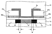
본 발명의 전기 광학 장치는, 상기 과제를 해결하기 위해, 기판과, 그 기판 상에서, 서로 교차하여 연재되는 데이터선 및 주사선과, 상기 데이터선 및 상기 주사선의 교차에 대응하여 규정되는 화소마다 형성된 화소 전극과, 상기 데이터선 또는 상기 주사선의 연재 방향을 따른 채널 길이를 갖는 채널 영역, 상기 데이터선에 전기적으로 접속된 데이터선측 소스 드레인 영역, 상기 화소 전극에 전기적으로 접 속된 화소 전극측 소스 드레인 영역, 상기 채널 영역 및 상기 데이터선측 소스 드레인 영역 간에 형성된 제 1 접합 영역, 그리고 상기 채널 영역 및 상기 화소 전극측 소스 드레인 영역 간에 형성된 제 2 접합 영역을 갖는 반도체층과, 상기 제 1 접합 영역을 덮도록 섬 형상으로 형성된 제 1 절연막과, 상기 제 2 접합 영역을 덮도록 섬 형상으로 형성된 제 2 절연막과, 상기 채널 영역에 게이트 절연막을 개재시켜 대향함과 함께, 상기 제 1 및 제 2 절연막 상에 연재되는 게이트 전극을 구비한다. In order to solve the said subject, the electro-optical device of this invention has the board | substrate, the data line and the scanning line which intersect and mutually cross each other, and the pixel formed in every pixel prescribed | regulated corresponding to the intersection of the said data line and the said scanning line. A channel region having an electrode, a channel length along the extending direction of the data line or the scan line, a data line side source drain region electrically connected to the data line, a pixel electrode side source drain region electrically connected to the pixel electrode, A semiconductor layer having a first junction region formed between the channel region and the data line side source drain region, and a second junction region formed between the channel region and the pixel electrode side source drain region and covering the first junction region; A first insulating film formed in a shape and an island shape so as to cover the second junction region The second insulating film and, by interposing a gate insulating film on the channel region with the opposite box, provided with a gate electrode extending on the first and second insulating films.
본 발명에 관련된 전기 광학 장치에 의하면, 그 동작시에, 예를 들어 데이터선으로부터 화소 전극으로의 화상 신호의 공급이 제어되면서 주사선으로부터 주사 신호가 공급되어, 소위 액티브 매트릭스 방식에 의한 화상 표시가 가능해진다. 또한, 화상 신호는 데이터선 및 화소 전극 간에 전기적으로 접속된 스위칭 소자인 트랜지스터가 주사선으로부터 공급되는 주사 신호에 따라 온-오프됨으로써, 소정의 타이밍으로 데이터선으로부터 트랜지스터를 통하여 화소 전극으로 공급된다. 화소 전극은 예를 들어 ITO (Indium Tin Oxide) 등의 투명 도전 재료로 이루어지는 투명 전극으로서, 데이터선 및 주사선의 교차에 대응하여, 기판 상에서 표시 영역이 되어야 하는 영역에 매트릭스 형상으로 복수 형성된다. According to the electro-optical device according to the present invention, during the operation, for example, the scanning signal is supplied from the scanning line while the supply of the image signal from the data line to the pixel electrode is controlled, so that image display by the so-called active matrix method is possible. Become. In addition, the image signal is turned on and off in accordance with the scan signal supplied from the scan line, the transistor which is a switching element electrically connected between the data line and the pixel electrode, thereby being supplied from the data line to the pixel electrode at a predetermined timing. The pixel electrode is a transparent electrode made of a transparent conductive material such as, for example, indium tin oxide (ITO), and is formed in plural in a matrix form in an area to be a display area on the substrate in correspondence with the intersection of the data line and the scan line.
상기 서술한 트랜지스터는 채널 영역, 데이터선측 소스 드레인 영역, 화소 전극측 소스 드레인 영역, 그리고 채널 영역 및 데이터선측 소스 드레인 영역 간에 형성된 제 1 접합 영역, 채널 영역 및 화소 전극측 소스 드레인 영역 간에 형성된 제 2 접합 영역을 갖는 반도체층과, 채널 영역에 중첩되는 게이트 전극과, 반도체 층 및 게이트 전극 간에 배치된 게이트 절연막에 의해 구축되어 있다. 또한, 트랜지스터는 반도체층을 상하로부터 2 개의 게이트 전극이 사이에 놓이거나 또는 2 개의 직렬로 접속된 채널 영역에 대해 2 개의 게이트 전극이 각각 존재하는 더블 게이트형 박막 트랜지스터가 구축되어도 된다. 또한, 3 개 이상의 게이트 전극이 있어도 된다. The above-described transistor includes a channel region, a data line side source drain region, a pixel electrode side source drain region, and a first junction region formed between the channel region and the data line side source drain region, a second region formed between the channel region and the pixel electrode side source drain region. The semiconductor layer has a junction region, a gate electrode overlapping the channel region, and a gate insulating film disposed between the semiconductor layer and the gate electrode. In the transistor, a double gate type thin film transistor in which two gate electrodes are sandwiched between the top and bottom of the semiconductor layer, or two gate electrodes are present for two channel regions connected in series may be constructed. In addition, there may be three or more gate electrodes.
본 발명에서는 특히, 제 1 접합 영역을 덮도록 섬 형상으로 형성된 제 1 절연막과, 제 2 접합 영역을 덮도록 섬 형상으로 형성된 제 2 절연막이 형성된다. 즉, 제 1 및 제 2 접합 영역은 각각 기판 상에서 평면적으로 보아 제 1 및 제 2 절연막에 의해 덮인다. 제 1 및 제 2 절연막은 예를 들어 이산화규소 (SiO2) 등의 산화막으로 이루어지고, 에칭에 의한 패터닝 등에 의해 성형된다. In the present invention, in particular, a first insulating film formed in an island shape to cover the first bonding region and a second insulating film formed in an island shape so as to cover the second bonding region are formed. That is, the first and second junction regions are respectively covered by the first and second insulating films in plan view on the substrate. The first and second insulating films are made of, for example, oxide films such as silicon dioxide (SiO 2 ), and are formed by patterning by etching or the like.
또, 반도체층에 있어서의 채널 영역에는 게이트 절연막을 개재시켜 게이트 전극이 형성된다. 게이트 전극은 상기 서술한 제 1 및 제 2 절연막 상으로까지 연재되도록 형성되어 있다. 즉, 게이트 전극은 채널 영역에 대향하는 부분에서는 게이트 절연막을 개재시켜 배치되고, 채널 영역에 인접된 제 1 접합 영역 및 제 2 접합 영역에 대향하는 부분에서는 제 1 및 제 2 절연막 각각을 개재시키거나, 또는 제 1 및 제 2 절연막에 추가하여 게이트 절연막 등의 절연막을 개재시켜 배치된다. 이 때문에 게이트 전극은 반도체층에 대해 채널 영역에서 국소적으로 근접하도록 배치되고, 제 1 및 제 2 접합 영역에서는 제 1 및 제 2 절연막이 존재하는 만큼 떨어진 위치에 배치된다. In addition, a gate electrode is formed in the channel region of the semiconductor layer via a gate insulating film. The gate electrode is formed to extend on the first and second insulating films described above. That is, the gate electrode is disposed through the gate insulating film in a portion facing the channel region, and interposes the first and second insulating films in a portion opposite to the first and second bonding regions adjacent to the channel region, or Or in addition to the first and second insulating films, interposing insulating films such as a gate insulating film. For this reason, the gate electrode is disposed so as to be locally proximate to the channel region with respect to the semiconductor layer, and in the first and second junction regions, the gate electrodes are disposed as far apart as the first and second insulating films exist.
만일 게이트 전극을 제 1 및 제 2 접합 영역에 대해 예를 들어 게이트 절연막의 막두께 정도까지 근접시키면, 이 전극 부분 또는 배선 부분이 접합 영역에 대해 크건 작건 게이트 전압과 동일 전위를 인가하는 전극으로서 기능한다. 즉, 접합 영역에서도 상정 밖의 캐리어 밀도의 변화가 발생된다. 이 때문에, 원래는 채널 영역에 게이트 전압이 인가되어 채널이 형성되는 것이 상정되어 있는 박막 트랜지스터에 있어서의 리크 전류의 발생, 온-오프 임계값의 변화 등으로 이어진다. If the gate electrode is brought close to the first and second junction regions, for example, up to the film thickness of the gate insulating film, the electrode portion or the wiring portion functions as an electrode to apply the same potential as the gate voltage, large or small, to the junction region. do. That is, a change in carrier density outside the assumption occurs in the junction region. For this reason, the leakage current, the change of the on-off threshold value, etc. in the thin film transistor which are supposed to form a channel by applying a gate voltage to a channel region originally are caused.
그런데, 본 발명에서는 특히 제 1 및 제 2 절연막이 형성되어 있기 때문에, 게이트 전극과 제 1 및 제 2 접합 영역이 상기 서술한 바와 같은 리크 전류의 발생, 온-오프 임계값의 변화 등을 일으킬 정도까지 근접되지 않는다. 따라서, 트랜지스터에 있어서의 동작 불량을 효과적으로 방지하는 것이 가능하다.However, in the present invention, especially since the first and second insulating films are formed, the gate electrode and the first and second junction regions cause the leakage current as described above, a change in the on-off threshold value, and the like. Not close. Therefore, it is possible to effectively prevent the malfunction of the transistor.
또한 본 발명에서는 특히 게이트 전극이 제 1 및 제 2 절연막 상으로까지 연재되도록 형성되어 있다. 즉 게이트 절연막은 기판 상에서 평면적으로 보아 제 1 및 제 2 접합 영역과 중첩되도록 배치되어 있다. 이 때문에, 제 1 및 제 2 접합 영역에 대해 게이트 전극보다 상층측으로부터 입사되려고 하는 광을 차광하는 것이 가능하다. 특히 반도체층에 있어서의 제 2 접합 영역은 광리크 전류가 발생하기 쉽다고 여겨지고 있다. 따라서, 제 2 접합 영역에 입사되려고 하는 광을 차광함으로써 보다 효과적으로 광리크 전류의 발생을 방지할 수 있다. In the present invention, in particular, the gate electrode is formed so as to extend on the first and second insulating films. In other words, the gate insulating film is disposed so as to overlap the first and second bonding regions in plan view on the substrate. For this reason, it is possible to shield the light which is going to be incident from the upper layer side with respect to the 1st and 2nd junction area | regions. In particular, the second junction region in the semiconductor layer is considered to be liable to generate a photoleak current. Therefore, the light leakage current can be prevented more effectively by shielding the light that is about to enter the second junction region.
또, 상기 서술한 바와 같은 우수한 차광 성능에 의해 별도로 차광막 등을 형성하지 않아도 충분한 차광을 행할 수 있다. 따라서, 각 화소의 비개구 영역 (즉, 화상을 표시하는 데에 사용되는 광이 통과하지 않는 영역) 의 배치 면적이 넓어져, 비개구 영역을 제외한 개구 영역이 보다 작아지는 것을 방지할 수 있다. 그 결과, 각 화소를 미세화해도 비교적 높은 개구율을 유지할 수 있게 된다. Further, due to the excellent light shielding performance as described above, sufficient light shielding can be performed without separately forming a light shielding film or the like. Therefore, the arrangement area of the non-opening area (i.e., the area where the light used to display the image does not pass) of each pixel is widened, and the opening area except the non-opening area can be prevented from becoming smaller. As a result, a relatively high aperture ratio can be maintained even if each pixel is made fine.
이상 설명한 바와 같이, 본 발명에 관련된 전기 광학 장치에 의하면, 트랜지스터의 동작 불량을 방지하면서, 트랜지스터에 있어서의 광리크 전류의 발생에서 기인하는 플리커 등의 표시 불량의 발생을 저감 또는 방지할 수 있다. 따라서, 본 발명의 전기 광학 장치용 기판에 의하면, 고품위의 화상 표시가 가능해진다. As described above, according to the electro-optical device according to the present invention, it is possible to reduce or prevent the occurrence of display defects such as flicker resulting from the generation of the optical leakage current in the transistor while preventing the operation failure of the transistor. Therefore, according to the board | substrate for electro-optical devices of this invention, high quality image display is attained.
본 발명의 전기 광학 장치의 일 양태에서는, 상기 기판 상에서 평면적으로 보아, 상기 제 1 절연막은 상기 데이터선측 소스 드레인 영역의 적어도 일부와 중첩되지 않도록 형성되어 있고, 상기 제 2 절연막은 상기 화소 전극측 소스 드레인 영역의 적어도 일부와 중첩되지 않도록 형성되어 있고, 상기 게이트 전극은 상기 데이터선측 소스 드레인 영역의 적어도 일부와 중첩되도록 연재되어 있으며, 상기 화소 전극측 소스 드레인 영역의 적어도 일부와 중첩되도록 연재되어 있다.In one aspect of the electro-optical device of the present invention, in plan view, the first insulating film is formed so as not to overlap at least part of the data line side source drain region, and the second insulating film is the pixel electrode side source. The gate electrode is formed to overlap at least a portion of the drain region, and the gate electrode extends to overlap at least a portion of the data line side source drain region, and extend to overlap at least a portion of the pixel electrode side source drain region.
이 양태에 의하면, 제 1 절연막은, 기판 상에서 평면적으로 보아 데이터선측 소스 드레인 영역의 적어도 일부와 중첩되지 않도록 형성되어 있으며, 게이트 전극은 제 1 절연막의 윤곽을 따르도록 하여 데이터선측 소스 드레인 영역의 적어도 일부와 중첩되도록 연재된다. 이 때문에, 반도체층에 있어서의 제 1 접합 영역에 대해 제 1 절연막을 개재시켜 떨어진 위치에 배치된 게이트 전극은, 데이터선측 소스 드레인 영역에 대해 예를 들어 게이트 절연막의 막두께 정도까지 근접하도록 배치된다. According to this aspect, the first insulating film is formed so as not to overlap at least a portion of the data line side source drain region in plan view on the substrate, and the gate electrode follows the contour of the first insulating film so that at least the It is serialized to overlap some parts. For this reason, the gate electrode arrange | positioned in the position which separated the 1st insulating film with respect to the 1st junction area | region in a semiconductor layer is arrange | positioned so that it may be close to the film thickness of a gate insulating film, for example with respect to a data line side source-drain area | region. .
또 한편으로, 제 2 절연막은 기판 상에서 평면적으로 보아 화소 전극측 소스 드레인 영역의 적어도 일부와 중첩되지 않도록 형성되어 있으며, 게이트 전극은 제 2 절연막의 윤곽을 따르도록 하여 화소 전극측 소스 드레인 영역의 적어도 일부와 중첩되도록 연재된다. 따라서, 상기 서술한 제 1 절연막의 경우와 마찬가지로, 게이트 전극은 화소 전극측 소스 드레인 영역에 대해 예를 들어 게이트 절연막의 막두께 정도까지 근접하도록 배치된다. On the other hand, the second insulating film is formed so as not to overlap at least a part of the pixel electrode side source drain region in plan view on the substrate, and the gate electrode follows the contour of the second insulating film so that at least the It is serialized to overlap some parts. Therefore, similarly to the case of the first insulating film described above, the gate electrode is arranged to be close to the pixel electrode side source drain region to, for example, the thickness of the gate insulating film.
또한, 데이터선측 소스 드레인 영역 및 화소 전극측 소스 드레인 영역은 고농도로 도핑된 도전층이다. 이 때문에, 상기 서술한 바와 같이, 게이트 전극이 데이터선측 소스 드레인 영역 또는 화소 전극측 소스 드레인 영역에 근접하도록 배치되었다 하더라도, 게이트 전극에 생기는 전계가 데이터선측 소스 드레인 영역 및 화소 전극측 소스 드레인 영역에 전기적인 영향을 주어 트랜지스터에 동작 불량이 발생하는 경우는 거의 또는 실용상 전혀 없다. In addition, the data line side source drain region and the pixel electrode side source drain region are conductive layers heavily doped. For this reason, as described above, even if the gate electrode is arranged to be close to the data line side source drain region or the pixel electrode side source drain region, the electric field generated in the gate electrode is applied to the data line side source drain region and the pixel electrode side source drain region. There is little or no practical use of electrical effects resulting in malfunction of transistors.
게이트 전극이 데이터선측 소스 드레인 영역 또는 화소 전극측 소스 드레인 영역에 근접하도록 배치됨으로써, 예를 들어 데이터선측 소스 드레인 영역 또는 화소 전극측 소스 드레인 영역의 상층측으로부터 제 1 및 제 2 접합 영역에 대해 비스듬하게 입사되려고 하는 광을 차광하는 것이 가능해진다. 따라서, 보다 효과적으로 광리크 전류의 발생에서 기인하는 플리커 등의 표시 불량의 발생을 저감 또는 방지할 수 있다. 따라서, 고품위의 화상 표시가 가능해진다. The gate electrode is disposed so as to be close to the data line side source drain region or the pixel electrode side source drain region, for example, so as to be oblique with respect to the first and second junction regions from the upper layer side of the data line side source drain region or the pixel electrode side source drain region. It is possible to shield light that is about to be incident. Therefore, it is possible to more effectively reduce or prevent the occurrence of display defects such as flicker due to the generation of the optical leakage current. Therefore, high quality image display becomes possible.
본 발명의 전기 광학 장치의 다른 양태에서는, 상기 게이트 절연막은 상기 채널 영역에 추가하여 상기 제 1 및 제 2 접합 영역에 대향하는 영역에 상기 제 1 및 제 2 절연막의 하지층으로서 형성되어 있다.In another aspect of the electro-optical device of the present invention, the gate insulating film is formed as a base layer of the first and second insulating films in a region opposite to the first and second bonding regions in addition to the channel region.
이 양태에 의하면, 게이트 절연막이 채널 영역에 추가하여 제 1 및 제 2 접합 영역에 대향하는 영역에도 형성되어 있다. 그리고, 게이트 절연막은 제 1 및 제 2 절연막의 하지층이 된다. 즉, 제 1 및 제 2 절연막은 각각 게이트 절연막의 상층에 배치된다. According to this aspect, the gate insulating film is formed in a region facing the first and second junction regions in addition to the channel region. The gate insulating film becomes an underlayer of the first and second insulating films. That is, the first and second insulating films are disposed on the upper layer of the gate insulating film, respectively.
이와 같이 구성함으로써, 게이트 전극은 반도체층에 대해 제 1 및 제 2 접합 영역에 대향하는 부분에서는 제 1 및 제 2 절연막의 두께만큼 떨어진 위치에 배치된다. 따라서, 게이트 전극에 생긴 전계가 제 1 및 제 2 접합 영역에 전기적인 영향을 주는 것을 보다 효과적으로 방지할 수 있다. 따라서, 트랜지스터에 있어서의 동작 불량을 보다 확실하게 방지하는 것이 가능하다. With this configuration, the gate electrode is disposed at a position separated by the thickness of the first and second insulating films in the portion facing the first and second bonding regions with respect to the semiconductor layer. Therefore, it is possible to more effectively prevent the electric field generated in the gate electrode from electrically affecting the first and second junction regions. Therefore, it is possible to more reliably prevent the malfunction of the transistor.
본 발명의 전기 광학 장치의 다른 양태에서는, 상기 게이트 절연막은 상기 제 1 및 제 2 접합 영역에 대향하는 영역에 형성되어 있지 않고, 상기 제 1 및 제 2 절연막은 각각 상기 게이트 절연막보다 두껍다.In another aspect of the electro-optical device of the present invention, the gate insulating film is not formed in a region facing the first and second bonding regions, and the first and second insulating films are thicker than the gate insulating film, respectively.
이 양태에 의하면, 게이트 절연막은 제 1 및 제 2 접합 영역에 대향하는 영역에 형성되어 있지 않다. 이 때문에, 제 1 및 제 2 절연막은 반도체층에 대해 게이트 절연막을 개재시키지 않고 대향 배치된다. According to this aspect, the gate insulating film is not formed in the region facing the first and second bonding regions. For this reason, the 1st and 2nd insulating films are arrange | positioned facing a semiconductor layer without interposing a gate insulating film.
여기에서 특히 제 1 및 제 2 절연막은 각각 게이트 절연막보다 두꺼워지도록 형성되어 있다. 이 때문에, 게이트 전극은 반도체층에 대해 제 1 및 제 2 접합 영역에 대향하는 부분에서는 제 1 및 제 2 절연막의 두께와 게이트 절연막의 두께의 차분만큼 떨어진 위치에 배치된다. 바꾸어 말하면, 게이트 전극은 제 1 및 제 2 접합 영역에 대향하는 부분에서는 채널 영역에 대향하는 부분과 비교하여 확실히 반도체층으로부터 떨어진 위치에 배치된다. 따라서, 게이트 전극에 생기는 전계가 제 1 및 제 2 접합 영역에 전기적인 영향을 주는 것을 보다 효과적으로 방지할 수 있다. 따라서, 트랜지스터에 있어서의 동작 불량을 보다 확실하게 방지하는 것이 가능하다. In particular, the first and second insulating films are formed to be thicker than the gate insulating film, respectively. For this reason, the gate electrode is disposed at a position spaced apart by the difference between the thickness of the first and second insulating films and the thickness of the gate insulating film in the portion facing the first and second bonding regions with respect to the semiconductor layer. In other words, the gate electrode is disposed at a position away from the semiconductor layer in a portion opposite to the first and second junction regions, as compared with the portion facing the channel region. Therefore, it is possible to more effectively prevent the electric field generated in the gate electrode from electrically affecting the first and second junction regions. Therefore, it is possible to more reliably prevent the malfunction of the transistor.
본 발명의 전기 광학 장치의 다른 양태에서는, 상기 제 1 및 제 2 절연막은 서로 동일 층에 동일 막으로 형성된다. In another aspect of the electro-optical device of the present invention, the first and second insulating films are formed on the same layer with the same film.
이 양태에 의하면, 제 1 및 제 2 절연막이 서로 동일 층에 동일 막으로 형성되기 때문에, 제 1 및 제 2 절연막을 동일한 성막 공정으로 형성하는 것이 가능해진다. 또한, 제 1 및 제 2 절연막은 동일한 성막 공정으로 형성되는 것이라면, 예를 들어 막의 두께 등은 서로 상이해도 된다. 제 1 및 제 2 절연막을 동일한 성막 공정으로 형성함으로써, 제조 공정의 장기화 및 복잡 고도화 등을 방지하는 것이 가능해진다. According to this embodiment, since the first and second insulating films are formed on the same layer with the same film, it is possible to form the first and second insulating films in the same film forming process. In addition, as long as the 1st and 2nd insulating films are formed by the same film forming process, the thickness of a film, etc. may differ, for example. By forming the first and second insulating films in the same film forming process, it is possible to prevent prolongation of the manufacturing process, increase in complexity, and the like.
본 발명의 전기 광학 장치의 다른 양태에서는, 상기 제 1 절연막은, 상기 기판 상에서 평면적으로 보아, 상기 제 1 접합 영역에 추가하여 상기 데이터선측 소스 드레인 영역을 적어도 부분적으로 덮도록 형성되어 있으며, 상기 게이트 전극은 상기 제 1 절연막에 있어서의 상기 데이터선측 소스 드레인 영역을 덮도록 연재되어 있다.In another aspect of the electro-optical device of the present invention, the first insulating film is formed so as to at least partially cover the data line side source drain region in addition to the first junction region in plan view on the substrate. An electrode is extended to cover the data line side source drain region in the first insulating film.
이 양태에 의하면, 제 1 절연막은, 기판 상에서 평면적으로 보아, 제 1 접합 영역에 추가하여 데이터선측 소스 드레인 영역을 적어도 부분적으로 덮도록 형성되 어 있다. 그리고, 게이트 전극은 제 1 절연막에 있어서의 데이터선측 소스 드레인 영역을 덮도록 연재되어 있다. 즉, 게이트 전극은, 기판 상에서 평면적으로 보아, 데이터선측 소스 드레인 영역에 적어도 부분적으로 중첩되도록 배치된다. 이 때문에 예를 들어 데이터선측 소스 드레인 영역의 상층측으로부터 제 1 접합 영역에 대해 비스듬하게 입사되려고 하는 광을 게이트 전극에 의해 차광하는 것이 가능해진다. 따라서, 보다 효과적으로 광리크 전류의 발생에서 기인하는 플리커 등의 표시 불량의 발생을 저감 또는 방지할 수 있다. 따라서, 고품위의 화상 표시가 가능해진다. According to this aspect, the first insulating film is formed so as to at least partially cover the data line side source drain region in addition to the first junction region in plan view on the substrate. The gate electrode is extended so as to cover the data line side source drain region in the first insulating film. That is, the gate electrode is disposed so as to be at least partially overlapped with the data line side source drain region in plan view on the substrate. For this reason, for example, it becomes possible to light-shield the light which is going to be obliquely incident on the first junction region from the upper layer side of the data line side source drain region by the gate electrode. Therefore, it is possible to more effectively reduce or prevent the occurrence of display defects such as flicker due to the generation of the optical leakage current. Therefore, high quality image display becomes possible.
본 발명의 전기 광학 장치의 다른 양태에서는, 상기 제 2 절연막은, 상기 기판 상에서 평면적으로 보아, 상기 제 2 접합 영역에 추가하여 상기 화소 전극측 소스 드레인 영역을 적어도 부분적으로 덮도록 형성되어 있으며, 상기 게이트 전극은 상기 제 2 절연막에 있어서의 상기 화소 전극측 소스 드레인 영역을 덮도록 연재되어 있다.In another aspect of the electro-optical device of the present invention, the second insulating film is formed so as to at least partially cover the pixel electrode side source drain region in addition to the second bonding region in plan view on the substrate. The gate electrode is extended to cover the source drain region of the pixel electrode side in the second insulating film.
이 양태에 의하면, 제 2 절연막은, 기판 상에서 평면적으로 보아, 제 2 접합 영역에 추가하여 화소 전극측 소스 드레인 영역을 적어도 부분적으로 덮도록 형성되어 있다. 그리고, 게이트 전극은 제 2 절연막에 있어서의 화소 전극측 소스 드레인 영역을 덮도록 연재되어 있다. 즉, 게이트 전극은, 기판 상에서 평면적으로 보아, 화소 전극측 소스 드레인 영역에 적어도 부분적으로 중첩되도록 배치된다. 이 때문에, 예를 들어 화소 전극측 소스 드레인 영역의 상층측으로부터 제 1 접합 영역에 대해 비스듬하게 입사되려고 하는 광을 게이트 전극에 의해 차광하 는 것이 가능해진다. 따라서, 보다 효과적으로 광리크 전류의 발생에서 기인하는 플리커 등의 표시 불량의 발생을 저감 또는 방지할 수 있다. 따라서, 고품위의 화상 표시가 가능해진다. 또, 채널 영역과 제 2 접합 영역의 계면에서 가장 광리크 전류가 발생하기 쉽다는 점에서, 이러한 양태에 의하면, 그 계면에서의 차광성의 향상을 도모할 수 있다. According to this aspect, the second insulating film is formed so as to at least partially cover the pixel electrode side source drain region in addition to the second bonding region in plan view on the substrate. The gate electrode is extended to cover the pixel electrode side source drain region in the second insulating film. That is, the gate electrode is disposed to be at least partially overlapped with the source drain region on the pixel electrode side in plan view on the substrate. For this reason, for example, it becomes possible to shield the light which is going to be obliquely incident on the first junction region from the upper layer side of the pixel electrode side source drain region by the gate electrode. Therefore, it is possible to more effectively reduce or prevent the occurrence of display defects such as flicker due to the generation of the optical leakage current. Therefore, high quality image display becomes possible. In addition, since the optical leakage current is most likely to occur at the interface between the channel region and the second junction region, the light shielding property at the interface can be improved according to this embodiment.
본 발명의 전기 광학 장치의 다른 양태에서는, 상기 제 1 및 제 2 절연막의 적어도 일방은, 상기 기판 상에서 평면적으로 보아, 상기 채널 영역으로부터 소정 거리 떨어진 위치에 배치되어 있다.In another aspect of the electro-optical device of the present invention, at least one of the first and second insulating films is disposed at a position away from the channel region in plan view on the substrate.
이 양태에 의하면, 제 1 및 제 2 절연막의 적어도 일방은, 기판 상에서 평면적으로 보아, 채널 영역으로부터 소정 거리 떨어진 위치에 배치된다. 또한, 여기에서의 「소정 거리」란 제 1 및 제 2 절연막이 채널 영역의 유지 특성에 영향을 주지 않는 거리이다. 구체적으로는 예를 들어 0.125㎛ 정도이고, 제조 마진 또는 패터닝 정밀도가 가미되어도 된다. According to this aspect, at least one of the 1st and 2nd insulating films is arrange | positioned in the position which is predetermined distance from the channel area seen planarly on a board | substrate. In addition, the "predetermined distance" here is the distance which the 1st and 2nd insulating film does not affect the holding | maintenance characteristic of a channel region. Specifically, it is about 0.125 micrometers, for example, and manufacturing margin or patterning precision may be added.
제 1 및 제 2 절연막을 채널 영역으로부터 소정 거리 떨어진 위치에 배치함으로써, 제 1 및 제 2 절연막이 채널 영역의 유지 특성에 영향을 주지 않도록 하는 것이 가능하다. 따라서, 트랜지스터가 온으로 되어 있을 때에, 채널 영역에 흐르는 전류 (즉, 온 전류) 의 저하를 방지할 수 있다. 따라서, 고품질의 화상을 표시하는 것이 가능해진다. By arranging the first and second insulating films at positions away from the channel region, it is possible to prevent the first and second insulating films from affecting the retention characteristics of the channel regions. Therefore, when the transistor is turned on, it is possible to prevent a decrease in the current flowing in the channel region (that is, the on current). Therefore, it becomes possible to display a high quality image.
본 발명의 전기 광학 장치의 다른 양태에서는, 상기 제 1 및 제 2 절연막의 적어도 일방은 상기 반도체층에 질화막을 개재시켜 대향하도록 배치되어 있다.In another aspect of the electro-optical device of the present invention, at least one of the first and second insulating films is disposed so as to face the semiconductor layer via a nitride film.
이 양태에 의하면, 반도체층과 제 1 및 제 2 절연막의 적어도 일방과의 사이에는 질화막이 형성되어 있다. 질화막은 예를 들어 제 1 및 제 2 절연막을 에칭에 의해 패터닝할 때 등에 보호막으로서 기능한다. 따라서, 과도한 에칭에 의해 게이트 절연막이나 반도체층이 손상되는 것을 방지할 수 있다. 따라서, 제조 공정의 복잡 고도화 등을 방지하는 것이 가능해진다. According to this aspect, a nitride film is formed between the semiconductor layer and at least one of the first and second insulating films. The nitride film functions as a protective film, for example, when patterning the first and second insulating films by etching. Therefore, it is possible to prevent the gate insulating film or the semiconductor layer from being damaged by excessive etching. Therefore, it becomes possible to prevent complicated advancement of a manufacturing process.
또한, 질화막은 차광 성능을 가지고 있기 때문에, 반도체층에 입사되려고 하는 광을 차광하는 것이 가능하다. 따라서, 반도체층에 있어서의 광리크 전류의 발생을 방지한다는 효과를 높이는 것도 가능하다. In addition, since the nitride film has light shielding performance, it is possible to shield light that is about to be incident on the semiconductor layer. Therefore, it is also possible to heighten the effect of preventing generation of the optical leakage current in the semiconductor layer.
본 발명의 전기 광학 장치의 다른 양태에서는, 상기 제 2 접합 영역은, 상기 기판 상에서 평면적으로 보아, 상기 데이터선 및 상기 주사선이 교차하는 교차 영역 내에 적어도 부분적으로 배치되어 있다.In another aspect of the electro-optical device of the present invention, the second bonding region is disposed at least partially within an intersection region where the data line and the scanning line cross each other in plan view.
이 양태에 의하면, 제 2 접합 영역은, 기판 상에서 평면적으로 보아, 주사선 및 데이터선이 교차하는 교차 영역 내에 적어도 부분적으로 배치되어 있다. 주사선 및 데이터선을 교차시킴으로써, 교차 영역에 있어서의 차광 성능은 향상된다. 따라서, 광리크 전류가 발생하기 쉽다고 여겨지고 있는 제 2 접합 영역을 차광 성능이 높은 교차 영역 내에 배치함으로써, 보다 효과적으로 광리크 전류의 발생을 방지할 수 있다. 따라서, 고품질의 화상을 표시하는 것이 가능해진다. According to this aspect, the second bonding region is disposed at least partially in an intersection region where the scanning lines and the data lines intersect in plan view. By intersecting the scanning lines and the data lines, the light shielding performance in the intersection area is improved. Therefore, by arrange | positioning the 2nd junction area | region which is considered to generate | occur | produce an optical leak current in the intersection area with high light shielding performance, generation | occurrence | production of an optical leak current can be prevented more effectively. Therefore, it becomes possible to display a high quality image.
본 발명의 전기 광학 장치의 다른 양태에서는, 상기 제 2 접합 영역은 LDD 영역이다.In another aspect of the electro-optical device of the present invention, the second junction region is an LDD region.
이 양태에 의하면, 반도체층이 LDD 영역 (즉, 예를 들어 이온 임플랜테이션 법 등의 불순물 주입에 의해 반도체층에 불순물을 주입하여 이루어지는 불순물 영역) 을 가지고 있으며, LDD 형 박막 트랜지스터로서 구축된다. 또한, 제 2 접합 영역에 추가하여, 제 1 접합 영역도 LDD 영역이어도 된다. According to this aspect, the semiconductor layer has an LDD region (i.e., an impurity region formed by implanting impurities into the semiconductor layer by impurity implantation, for example, ion implantation method), and is constructed as an LDD type thin film transistor. In addition to the second bonding region, the first bonding region may also be an LDD region.
만일 제 2 접합 영역으로서 형성된 LDD 영역 (이하, 적당히 「화소 전극측 LDD 영역」이라고 한다) 에 광리크 전류가 발생되면, LDD 구조를 갖는 트랜지스터의 특성상, 트랜지스터가 오프로 되어 있을 때에, 데이터선측 소스 드레인 영역 및 화소 전극측 소스 드레인 영역에 흐르는 전류 (즉, 오프 전류) 가 증가한다. If the optical leakage current is generated in the LDD region (hereinafter referred to as "pixel electrode side LDD region" suitably) formed as the second junction region, the data line side source when the transistor is turned off due to the characteristics of the transistor having the LDD structure. Current (that is, off current) flowing in the drain region and the pixel electrode side source drain region increases.
그런데, 본 양태에서는 특히, 화소 전극측 LDD 영역에 입사되는 광을 게이트 전극에 의해 효과적으로 차광할 수 있다. 따라서, 상기 서술한 바와 같은 오프 전류의 증가를 효과적으로 방지할 수 있어, 고품질의 화상을 표시하는 것이 가능해진다.By the way, especially in this aspect, the light incident on the pixel electrode side LDD region can be shielded effectively by the gate electrode. Therefore, the increase of the off current as mentioned above can be prevented effectively, and it becomes possible to display a high quality image.
본 발명의 전자 기기는 상기 과제를 해결하기 위해, 상기 서술한 본 발명의 전기 광학 장치를 구비하여 이루어진다.In order to solve the said subject, the electronic device of this invention is equipped with the electro-optical device of this invention mentioned above.
본 발명의 전자 기기에 의하면, 상기 서술한 본 발명의 전기 광학 장치 (단, 그 각종 양태도 포함한다) 를 구비하여 이루어지기 때문에, 고품질의 표시를 행할 수 있는 투사형 표시 장치, 휴대 전화, 전자 수첩, 워드 프로세서, 뷰파인더형 또는 모니터 직시형 비디오 테이프 리코더, 워크스테이션, 텔레비전 전화, POS 단말, 터치 패널 등의 각종 전자 기기를 실현할 수 있다. 또, 본 발명에 관련된 전자 기기로서, 예를 들어 전자 페이퍼 등의 전기 영동 장치 등도 실현하는 것이 가능하다.According to the electronic device of the present invention, the electro-optical device (including various aspects thereof) of the present invention described above is provided, and therefore, a projection display device, a mobile phone, an electronic notebook capable of high-quality display can be provided. Various electronic devices such as a word processor, a viewfinder type or a monitor direct view video tape recorder, a workstation, a television telephone, a POS terminal, and a touch panel can be realized. Moreover, as an electronic device which concerns on this invention, electrophoretic apparatuses, such as an electronic paper, etc. can also be implement | achieved.
본 발명의 전기 광학 장치의 제조 방법은, 상기 과제를 해결하기 위해, 기판 상에 채널 영역, 데이터선측 소스 드레인 영역, 화소 전극측 소스 드레인 영역, 상기 채널 영역 및 상기 데이터선측 소스 드레인 영역 간에 형성된 제 1 접합 영역, 그리고 상기 채널 영역 및 상기 화소 전극측 소스 드레인 영역 간에 형성된 제 2 접합 영역을 갖는 반도체층을 형성하는 공정과, 상기 기판 상에서 평면적으로 보아, 상기 반도체층을 덮도록 게이트 절연막을 형성하는 공정과, 상기 기판 상에서 평면적으로 보아, 상기 게이트 절연막을 덮도록 형성된 절연막을 패터닝하여, 상기 기판 상에서 평면적으로 보아, 상기 제 1 접합 영역을 덮도록 섬 형상으로 형성된 제 1 절연막, 및 상기 제 2 접합 영역을 덮도록 형성된 제 2 절연막을 형성하는 공정과, 상기 채널 영역에 게이트 절연막을 개재시켜 대향하도록, 그리고 상기 기판 상에서 평면적으로 보아, 상기 제 1 및 제 2 절연막 상에 연재되도록 게이트 전극을 형성하는 공정과, 서로 교차하여 연재되도록 주사선 및 데이터선을 형성하는 공정과, 상기 주사선 및 상기 데이터선의 교차에 대응하여 규정되는 화소마다 화소 전극을 형성하는 공정을 구비한다.In order to solve the above problems, a method of manufacturing an electro-optical device according to the present invention includes a channel formed between a channel region, a data line side source drain region, a pixel electrode side source drain region, the channel region and the data line side source drain region. Forming a semiconductor layer having a first junction region and a second junction region formed between the channel region and the pixel electrode side source drain region; and forming a gate insulating film so as to cover the semiconductor layer in plan view on the substrate. And a first insulating film formed in an island shape so as to cover the first junction region in plan view on the substrate, by patterning an insulating film formed on the substrate to cover the gate insulating film. Forming a second insulating film formed so as to cover a region; Forming a gate electrode so as to face each other via the insulating film and planarly on the substrate, and forming a scanning line and a data line so as to cross and intersect with each other; And forming a pixel electrode for each pixel defined corresponding to the intersection of the scan line and the data line.
본 발명에 관련된 전기 광학 장치의 제조 방법에 의하면, 먼저 기판 상에 채널 영역, 데이터선측 소스 드레인 영역, 화소 전극측 소스 드레인 영역, 채널 영역 및 데이터선측 소스 드레인 영역 간에 형성된 제 1 접합 영역, 그리고 채널 영역 및 화소 전극측 소스 드레인 영역 간에 형성된 제 2 접합 영역을 갖는 반도체층이 형성되고, 계속해서 기판 상에서 평면적으로 보아, 반도체층을 덮도록 게이트 절연막이 형성된다. According to the method of manufacturing an electro-optical device according to the present invention, first, a first junction region formed between a channel region, a data line side source drain region, a pixel electrode side source drain region, a channel region and a data line side source drain region, and a channel A semiconductor layer having a second junction region formed between the region and the pixel electrode side source drain region is formed, and then a gate insulating film is formed so as to cover the semiconductor layer in plan view on the substrate.
다음으로, 기판 상에서 평면적으로 보아, 게이트 절연막을 덮도록 절연막이 형성된다. 절연막은 패터닝되어, 기판 상에서 평면적으로 보아, 제 1 접합 영역을 덮도록 섬 형상으로 형성된 제 1 절연막, 및 제 2 접합 영역을 덮도록 형성된 제 2 절연막이 형성된다. 또한, 채널 영역에 게이트 절연막을 개재시켜 대향하도록, 또한 기판 상에서 평면적으로 보아, 제 1 및 제 2 절연막 상으로까지 연재되도록 게이트 전극이 형성된다. 게이트 전극은 미리 제 1 및 제 2 절연막이 형성됨으로써, 반도체층에 입사되려고 하는 광을 효과적으로 차광할 수 있도록, 그리고 채널 영역 이외에 전기적인 영향을 주지 않도록 형성된다. Next, the insulating film is formed so as to cover the gate insulating film in plan view on the substrate. The insulating film is patterned to form a planar view on the substrate to form a first insulating film formed in an island shape so as to cover the first bonding region, and a second insulating film formed to cover the second bonding region. In addition, the gate electrode is formed so as to face the channel region via the gate insulating film, and to extend onto the first and second insulating films in plan view on the substrate. The first and second insulating films are formed in advance, so that the gate electrode can effectively shield light that is about to be incident on the semiconductor layer, and is formed so as not to have an electrical influence other than the channel region.
마지막으로 서로 교차하여 연재되도록 주사선 및 데이터선이 형성되고, 주사선 및 데이터선의 교차에 대응하여 규정되는 화소마다 화소 전극이 형성된다. Finally, a scan line and a data line are formed so as to cross each other, and a pixel electrode is formed for each pixel defined corresponding to the intersection of the scan line and the data line.
이상 설명한 바와 같이, 본 발명에 관련된 전기 광학 장치의 제조 방법에 의하면, 상기 서술한 고품위의 화상 표시가 가능한 전기 광학 장치를 바람직하게 제조하는 것이 가능하다. As explained above, according to the manufacturing method of the electro-optical device which concerns on this invention, it is possible to manufacture the electro-optical device which can display the high quality image mentioned above preferably.
본 발명의 전기 광학 장치의 제조 방법의 일 양태에서는, 상기 반도체층을 형성하는 공정은, 상기 채널 영역, 상기 데이터선측 소스 드레인 영역, 상기 화소 전극측 소스 드레인 영역, 그리고 상기 제 1 및 제 2 접합 영역이 형성되기 전의 반도체층에 저농도의 이온을 주입함으로써, LDD 영역으로서 상기 제 1 및 제 2 접합 영역을 형성하는 공정과, 상기 제 1 및 제 2 접합 영역이 형성된 반도체층에 고농도의 이온을 주입함으로써, 상기 데이터선측 소스 드레인 영역 및 상기 화소 전극측 소스 드레인 영역을 형성하는 공정을 포함한다.In one aspect of the manufacturing method of the electro-optical device of the present invention, the step of forming the semiconductor layer includes the channel region, the data line side source drain region, the pixel electrode side source drain region, and the first and second junctions. By implanting low concentration ions into the semiconductor layer before the region is formed, forming the first and second junction regions as LDD regions, and implanting high concentration ions into the semiconductor layer on which the first and second junction regions are formed. Thereby forming the data line side source drain region and the pixel electrode side source drain region.
이 양태에 의하면, 채널 영역, 데이터선측 소스 드레인 영역, 화소 전극측 소스 드레인 영역, 그리고 제 1 및 제 2 접합 영역이 형성되기 전의 반도체층에 대해 저농도의 이온이 주입된다. 이로써, 제 1 및 제 2 접합 영역이 LDD 영역으로서 형성된다. 또, 제 1 및 제 2 접합 영역이 형성됨으로써, 제 1 및 제 2 접합 영역 간에 형성되는 채널 영역도 규정되게 된다. 이온 주입시에는 LDD 영역으로 하지 않는 부분 (예를 들어 채널 영역) 에는 예를 들어 마스크를 형성해 두어, 이온이 주입되지 않도록 한다. According to this aspect, low concentration ions are implanted into the channel region, the data line side source drain region, the pixel electrode side source drain region, and the semiconductor layer before the first and second junction regions are formed. As a result, the first and second junction regions are formed as LDD regions. In addition, by forming the first and second junction regions, the channel region formed between the first and second junction regions is also defined. During ion implantation, for example, a mask is formed in a portion (e.g., a channel region) that does not serve as an LDD region so that ions are not implanted.
또한, 제 1 및 제 2 접합 영역이 형성된 후에는 반도체층에 고농도의 이온이 주입된다. 이로써, 데이터선측 소스 드레인 영역 및 화소 전극측 소스 드레인 영역이 형성된다. 데이터선측 소스 드레인 영역 및 화소 전극측 소스 드레인 영역은 고농도로 도핑된 영역으로서 형성되기 때문에, 상기 서술한 저농도의 이온이 주입되어 있어도 되고, 주입되어 있지 않아도 된다. 반대로, 채널 영역 및 제 1 및 제 2 접합 영역에는 고농도의 이온이 주입되지 않도록 실시한다. 또한, 상기 서술한 바와 같은 공정은 전형적으로는 게이트 절연막을 형성한 후에 행해진다. In addition, after the first and second junction regions are formed, a high concentration of ions are implanted into the semiconductor layer. As a result, a data line side source drain region and a pixel electrode side source drain region are formed. Since the data line side source drain region and the pixel electrode side source drain region are formed as highly doped regions, the above-described low concentration of ions may or may not be implanted. On the contrary, a high concentration of ions are not injected into the channel region and the first and second junction regions. In addition, the process as mentioned above is typically performed after forming a gate insulating film.
이상 설명한 바와 같이, 반도체층에 저농도의 이온과 고농도의 이온의 주입을 실시함으로써, 보다 바람직하게 LDD 영역을 갖는 반도체층을 형성할 수 있다. As described above, by injecting low-concentration ions and high-concentration ions into the semiconductor layer, a semiconductor layer having an LDD region can be formed more preferably.
본 발명의 전기 광학 장치의 제조 방법의 다른 양태에서는, 상기 게이트 절연막을 형성하는 공정 후에, 상기 기판 상에서 평면적으로 보아, 상기 게이트 절연막을 덮도록 질화막을 형성하는 공정과, 상기 제 1 및 제 2 절연막을 형성하는 공 정 후에, 열인산 처리에 의해 상기 질화막을 제거하는 공정을 추가로 구비한다.In another aspect of the manufacturing method of the electro-optical device of the present invention, after the step of forming the gate insulating film, a step of forming a nitride film so as to cover the gate insulating film in plan view on the substrate, and the first and second insulating films After the process of forming a film, the step of removing the nitride film by thermal phosphoric acid treatment is further provided.
이 양태에 의하면, 게이트 절연막이 형성되면, 기판 상에서 평면적으로 보아, 게이트 절연막을 덮도록 질화막이 형성된다. 이 때문에, 상기 서술한 제 1 및 제 2 절연막은 질화막의 상층에 형성된다. 여기에서, 질화막은 예를 들어 제 1 및 제 2 절연막을 에칭에 의해 패터닝할 때 등에 보호막으로서 기능한다. 따라서, 과도한 에칭에 의해 게이트 절연막이나 반도체층이 손상되는 것을 방지할 수 있다. 따라서, 제조 공정의 복잡 고도화 등을 방지하는 것이 가능해진다. According to this aspect, when the gate insulating film is formed, a nitride film is formed so as to cover the gate insulating film in plan view on the substrate. For this reason, the 1st and 2nd insulating films mentioned above are formed in the upper layer of a nitride film. Here, the nitride film functions as a protective film, for example, when patterning the first and second insulating films by etching. Therefore, it is possible to prevent the gate insulating film or the semiconductor layer from being damaged by excessive etching. Therefore, it becomes possible to prevent complicated advancement of a manufacturing process.
제 1 및 제 2 절연막이 형성된 후에는, 질화막은 열인산 처리에 의해 제거된다. 열인산 처리는 예를 들어 섭씨 120 도 내지 130 도의 인산을 사용하여 20 분 정도의 시간을 들여서 행해진다. 이 때에 제 1 및 제 2 절연막은 예를 들어 산화막과 같은 열인산의 영향을 받지 않는 재료로 구성된다. 따라서, 열인산에 의해 질화막이 제거되고, 제 1 및 제 2 절연막은 남는다. 이와 같이, 열인산 처리를 실시함으로써 보다 용이하게 질화막의 제거를 실시할 수 있다. 또한, 제 1 및 제 2 절연막과 게이트 절연막 사이에 형성된 질화막 (즉, 제 1 및 제 2 절연막에 의해 보호되어, 열인산의 영향을 받지 않은 질화막) 은 남게 되는데, 질화막은 차광 성능을 가지고 있기 때문에, 반도체층에 입사되려고 하는 광을 차광하는 차광막으로서 기능하게 할 수 있다. 따라서, 반도체층에 있어서의 광리크 전류의 발생을 방지한다고 하는 효과를 높이는 것도 가능하다. After the first and second insulating films are formed, the nitride film is removed by thermal phosphoric acid treatment. The thermal phosphoric acid treatment is carried out by taking about 20 minutes using, for example, phosphoric acid at 120 degrees Celsius to 130 degrees Celsius. At this time, the first and second insulating films are made of a material which is not affected by thermal phosphoric acid, for example, an oxide film. Thus, the nitride film is removed by thermal phosphoric acid, leaving the first and second insulating films. In this way, the nitride film can be more easily removed by performing the thermal phosphoric acid treatment. In addition, a nitride film formed between the first and second insulating films and the gate insulating film (that is, a nitride film protected by the first and second insulating films and not affected by thermal phosphoric acid) remains, but the nitride film has light shielding performance. Can function as a light shielding film for shielding light that is about to enter the semiconductor layer. Therefore, it is also possible to heighten the effect of preventing generation of the optical leakage current in the semiconductor layer.
본 발명의 작용 및 다른 이득은 다음에 설명하는 실시하기 위한 최선의 형태로부터 명백해진다. The operation and other benefits of the present invention will become apparent from the best mode for carrying out the following description.
본 발명에 의하면, 트랜지스터의 동작 불량을 방지하면서 광리크 전류의 발생을 저감시킬 수 있으며, 고품질의 화상을 표시할 수 있는 전기 광학 장치 및 그 제조 방법, 그리고 그 전기 광학 장치를 구비하여 이루어지는 전자 기기를 제공할 수 있다.According to the present invention, an electro-optical device and a manufacturing method thereof, and an electro-optical device comprising the electro-optical device, which can reduce the generation of the optical leakage current while preventing the malfunction of the transistor, can display a high quality image. Can be provided.
이하에서는, 본 발명의 각 실시형태에 대하여 도면을 참조하면서 설명한다. 이하의 실시형태에서는 각각 본 발명의 전기 광학 장치의 일례인 구동 회로 내장형의 TFT 액티브 매트릭스 구동 방식의 액정 장치를 예로 든다.Hereinafter, each embodiment of this invention is described, referring drawings. In the following embodiment, the liquid crystal device of the TFT active-matrix drive system with a built-in drive circuit which is an example of the electro-optical device of this invention is taken as an example, respectively.
<전기 광학 장치><Electro-optical device>
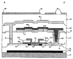
먼저, 본 실시형태에 관련된 액정 장치의 전체 구성에 대하여 도 1 및 도 2 를 참조하여 설명한다. 여기에서, 도 1 은 TFT 어레이 기판을 그 위에 형성된 각 구성 요소와 함께 대향 기판측에서 본 액정 장치의 개략적인 평면도이고, 도 2 는 도 1 의 H-H' 선 단면도이다. First, the whole structure of the liquid crystal device which concerns on this embodiment is demonstrated with reference to FIG. 1 and FIG. Here, FIG. 1 is a schematic plan view of the liquid crystal device seen from the opposing substrate side with the TFT array substrate with each component formed thereon, and FIG. 2 is a sectional view taken along the line H-H 'of FIG.
도 1 및 도 2 에 있어서, 본 실시형태에 관련된 액정 장치는 대향 배치된 TFT 어레이 기판 (10) 과 대향 기판 (20) 으로 구성되어 있다. TFT 어레이 기판 (10) 은 예를 들어 석영 기판, 유리 기판, 실리콘 기판 등의 투명 기판이다. 대향 기판 (20) 도 예를 들어, TFT 어레이 기판 (10) 과 동일한 재료로 이루어지는 투명 기판이다. TFT 어레이 기판 (10) 과 대향 기판 (20) 사이에는 액정층 (50) 이 밀봉되어 있으며, TFT 어레이 기판 (10) 과 대향 기판 (20) 은 화상 표시 영역 (10a) 의 주위에 위치하는 시일 영역에 형성된 시일재 (52) 에 의해 서로 접착되어 있다. In FIG. 1 and FIG. 2, the liquid crystal device which concerns on this embodiment is comprised from the
시일재 (52) 는 양 기판을 부착시키기 위한, 예를 들어 자외선 경화 수지, 열경화 수지 등으로 이루어지고, 제조 프로세스에 있어서 TFT 어레이 기판 (10) 상에 도포된 후, 자외선 조사, 가열 등에 의해 경화된 것이다. 또, 예를 들어 시일재 (52) 중에는 TFT 어레이 기판 (10) 과 대향 기판 (20) 의 간격 (기판 간 갭) 을 소정 값으로 하기 위한 유리 파이버 또는 유리 비즈 등의 갭재 (56) 가 산포되어 있다. 본 실시형태에 관련된 액정 장치는 프로젝터의 라이트 밸브용으로서 소형으로 확대 표시를 행하는 데에 적합하다. The
시일재 (52) 가 배치된 시일 영역의 내측에 병행하여, 화상 표시 영역 (10a) 의 프레임 영역을 규정하는 차광성의 프레임 차광막 (53) 이 대향 기판 (20) 측에 형성되어 있다. 단, 이러한 프레임 차광막 (53) 의 일부 또는 전부는 TFT 어레이 기판 (10) 측에 내장 차광막으로서 형성되어도 된다. A light shielding frame
TFT 어레이 기판 (10) 상에 있어서의, 화상 표시 영역 (10a) 의 주변에 위치하는 주변 영역에는 데이터선 구동 회로 (101) 및 샘플링 회로 (7), 주사선 구동 회로 (104), 외부 회로 접속 단자 (102) 가 각각 형성된다. The data
TFT 어레이 기판 (10) 상에 있어서의 주변 영역에 있어서, 시일 영역보다 외주측에 데이터선 구동 회로 (101) 및 외부 회로 접속 단자 (102) 가 TFT 어레이 기판 (10) 의 1 변을 따라 형성되어 있다. 또, TFT 어레이 기판 (10) 상의 주변 영역 중 시일 영역보다 내측에 위치하는 영역에는 TFT 어레이 기판 (10) 의 1 변을 따르는 화상 표시 영역 (10a) 의 1 변을 따라 그리고 프레임 차광막 (53) 에 덮이도록 하여 샘플링 회로 (7) 가 배치된다. In the peripheral region on the
주사선 구동 회로 (104) 는 TFT 어레이 기판 (10) 의 1 변에 인접하는 2 변을 따라, 그리고 프레임 차광막 (53) 에 덮이도록 하여 형성되어 있다. 또한, 이와 같이 화상 표시 영역 (10a) 의 양측에 형성된 2 개의 주사선 구동 회로 (104) 사이를 전기적으로 접속하기 위해, TFT 어레이 기판 (10) 의 남는 1 변을 따라, 그리고 프레임 차광막 (53) 에 덮이도록 하여 복수의 배선 (105) 이 형성되어 있다. The scanning
또, TFT 어레이 기판 (10) 상의 주변 영역에 있어서, 대향 기판 (20) 의 4 개의 코너부에 대향하는 영역에 상하 도통 단자 (106) 가 배치됨과 함께, 이 TFT 어레이 기판 (10) 및 대향 기판 (20) 간에는 상하 도통재가 상하 도통 단자 (106) 에 대응하여 그 단자 (106) 에 전기적으로 접속되어 형성된다. In the peripheral region on the
도 2 에 있어서, TFT 어레이 기판 (10) 상에는 구동 소자인 화소 스위칭용 TFT 나 주사선, 데이터선 등의 배선이 만들어진 적층 구조가 형성된다. 화상 표시 영역 (10a) 에는 화소 스위칭용 TFT 나 주사선, 데이터선 등의 배선의 상층에 화소 전극 (9a) 이 매트릭스 형상으로 형성되어 있다. 화소 전극 (9a) 상에는 배향막 (16) 이 형성되어 있다. 또한, 본 실시형태에서는 화소 스위칭 소자는 TFT 외에, 각종 트랜지스터 또는 TFD 등에 의해 구성되어도 된다.In Fig. 2, on the
한편, 대향 기판 (20) 에 있어서의 TFT 어레이 기판 (10) 과의 대향면 상에 차광막 (23) 이 형성되어 있다. 차광막 (23) 은 예를 들어 차광성 금속막 등으로 형성되어 있으며, 대향 기판 (20) 상의 화상 표시 영역 (10a) 내에서, 예를 들 어 격자 형상 등으로 패터닝되어 있다. 그리고, 차광막 (23) 상 (도 2 중 차광막 (23) 보다 하측) 에 ITO 등의 투명 재료로 이루어지는 대향 전극 (21) 이 복수의 화소 전극 (9a) 과 대향하여 예를 들어 베타 형상으로 형성되어 있으며, 또한 대향 전극 (21) 상 (도 2 중 대향 전극 (21) 보다 하측) 에는 배향막 (22) 이 형성되어 있다. On the other hand, the
액정층 (50) 은 예를 들어 1 종 또는 복수 종의 네마틱 액정을 혼합한 액정으로 이루어지고, 이들 1 쌍의 배향막 간에서 소정의 배향 상태를 취한다. 그리고, 액정 장치의 구동시, 각각에 전압이 인가됨으로써, 화소 전극 (9a) 과 대향 전극 (21) 사이에는 액정 유지 용량이 형성된다. The
또한, 여기에서는 도시하고 있지 않지만, TFT 어레이 기판 (10) 상에는 데이터선 구동 회로 (101), 주사선 구동 회로 (104) 외에, 복수의 데이터선에 소정 전압 레벨의 프리차지 신호를 화상 신호에 선행하여 각각 공급하는 프리차지 회로, 제조 도중이나 출하시의 당해 액정 장치의 품질, 결함 등을 검사하기 위한 검사 회로 등이 형성되어 있어도 된다.Although not shown here, on the
다음으로, 본 실시형태에 관련된 액정 장치의 화소부의 전기적인 구성에 대하여 도 3 을 참조하여 설명한다. 여기에서, 도 3 은 본 실시형태에 관련된 액정 장치의 화상 표시 영역을 구성하는 매트릭스 형상으로 형성된 복수의 화소에 있어서의 각종 소자, 배선 등의 등가 회로도이다. Next, the electrical structure of the pixel part of the liquid crystal device which concerns on this embodiment is demonstrated with reference to FIG. Here, FIG. 3 is an equivalent circuit diagram of the various elements, wirings, etc. in the several pixel formed in the matrix form which comprises the image display area of the liquid crystal device which concerns on this embodiment.
도 3 에 있어서, 화상 표시 영역 (10a) 을 구성하는 매트릭스 형상으로 형성된 복수의 화소 각각에는 화소 전극 (9a) 및 TFT (30) 가 형성되어 있다. TFT (30) 는 화소 전극 (9a) 에 전기적으로 접속되어 있으며, 액정 장치의 동작시에 화소 전극 (9a) 을 스위칭 제어한다. 화상 신호가 공급되는 데이터선 (6a) 은 TFT (30) 의 소스에 전기적으로 접속되어 있다. 데이터선 (6a) 에 기록하는 화상 신호 (S1, S2, …, Sn) 는, 이 순서로 선 순차적으로 공급해도 상관없고, 서로 인접하는 복수의 데이터선 (6a) 끼리에 대해 그룹마다 공급하도록 해도 된다.In FIG. 3, a
TFT (30) 의 게이트에는 주사선 (11a) 이 전기적으로 접속되어 있으며, 본 실시형태에 관련된 액정 장치는 소정의 타이밍으로 주사선 (11a) 에 펄스적으로 주사 신호 (G1, G2, …, Gm) 를 이 순서로 선 순차적으로 인가하도록 구성되어 있다. 화소 전극 (9a) 은 TFT (30) 의 드레인에 전기적으로 접속되어 있으며, 스위칭 소자인 TFT (30) 를 일정 기간만큼 그 스위치를 닫음으로써, 데이터선 (6a) 으로부터 공급되는 화상 신호 (S1, S2, …, Sn) 가 소정의 타이밍으로 기록된다. 화소 전극 (9a) 을 개재시켜 전기 광학 물질의 일례로서의 액정에 기록된 소정 레벨의 화상 신호 (S1, S2, …, Sn) 는 대향 기판에 형성된 대향 전극과의 사이에서 일정 기간 유지된다.The
액정층 (50) (도 2 참조) 을 구성하는 액정은 인가되는 전압 레벨에 따라 분자 집합의 배향이나 질서가 변화됨으로써 광을 변조하여, 계조 표시를 가능하게 한다. 노멀리 화이트 모드라면 각 화소의 단위로 인가된 전압에 따라 입사광에 대한 투과율이 감소되고, 노멀리 블랙 모드라면 각 화소의 단위로 인가된 전압에 따라 입사광에 대한 투과율이 증가되어, 전체적으로 액정 장치로부터는 화상 신호에 따른 콘트라스트를 갖는 광이 출사된다. The liquid crystal constituting the liquid crystal layer 50 (see FIG. 2) modulates light by changing the orientation and order of the molecular set according to the voltage level applied, thereby enabling gray scale display. In the normally white mode, the transmittance of incident light is decreased according to the voltage applied in units of pixels, and in the normally black mode, the transmittance of incident light is increased in accordance with the voltage applied in units of pixels, and the overall The light having contrast in accordance with the image signal is emitted.
여기에서 유지된 화상 신호가 리크되는 것을 방지하기 위해, 화소 전극 (9a) 과 대향 전극 (21) (도 2 참조) 사이에 형성되는 액정 용량에 대해 전기적으로 병렬로 축적 용량 (70) 이 부가되어 있다. 축적 용량 (70) 은 화상 신호의 공급에 따라 각 화소 전극 (9a) 의 전위를 일시적으로 유지하는 유지 용량으로서 기능하는 용량 소자이다. 축적 용량 (70) 의 일방의 전극은 화소 전극 (9a) 과 전기적으로 병렬하여 TFT (30) 의 드레인에 전기적으로 접속되고, 타방의 전극은 정전위가 되도록 전위 고정의 용량선 (300) 에 전기적으로 접속되어 있다. 축적 용량 (70) 에 의하면, 화소 전극 (9a) 에 있어서의 전위 유지 특성이 향상되어, 콘트라스트 향상이나 플리커의 저감과 같은 표시 특성의 향상이 가능해진다. 또한, 축적 용량 (70) 은, 후술하는 바와 같이, TFT (30) 로 입사되는 광을 차단하는 내장 차광막으로서도 기능한다. In order to prevent leakage of the image signal held here, the
다음으로, 상기 서술한 동작을 실현시키는 화소부의 구체적인 구성에 대하여, 도 1 내지 도 3 에 추가하여 도 4 내지 도 9 를 참조하여 설명한다. 여기에서 도 4 는 서로 인접하는 복수의 화소부를 나타내는 평면도이고, 도 5 는 트랜지스터에 주목하여 그 구성을 나타내는 평면도이다. 또, 도 6 은 도 4 의 A-A' 선 단면도이고, 도 7 은 도 6 에 있어서의 트랜지스터 부분의 확대도이다. 또한, 도 8 은 본 실시형태에 관련된 액정 장치의 변형예를 나타내는 평면도이고, 도 9 는 도 4 의 B-B' 선 단면도이다. Next, the specific structure of the pixel part which realizes the above-mentioned operation is demonstrated with reference to FIGS. 4-9 in addition to FIGS. FIG. 4 is a plan view showing a plurality of pixel portions adjacent to each other, and FIG. 5 is a plan view showing a configuration with attention to a transistor. 6 is a cross-sectional view taken along line AA ′ of FIG. 4, and FIG. 7 is an enlarged view of a transistor portion in FIG. 6. 8 is a plan view showing a modification of the liquid crystal device according to the present embodiment, and FIG. 9 is a cross-sectional view taken along line B-B 'of FIG. 4.
또한, 도 4 내지 도 9 에서는 각 층ㆍ각 부재를 도면 상에서 인식할 수 있을 정도의 크기로 하기 위해, 그 각 층ㆍ각 부재마다 축척을 달리하고 있다. 이 점에 대해서는, 후술하는 해당하는 각 도면에 대하여 동일하다. 도 4 내지 도 9 에서는, 도 1 또는 도 2 를 참조하여 설명한 구성 중 TFT 어레이 기판측의 구성에 대해서만 설명하는데, 설명의 편의상, 이들 도면에서는 화소 전극 (9a) 보다 상측에 위치하는 부분의 도시를 생략하고 있다. 또, 도 5 에서는 트랜지스터에 주목하여, 그 구성을 보다 상세하게 나타냄과 함께, 비개구 영역에 있어서의 트랜지스터에 대한 데이터선이나 주사선, 축적 용량을 구성하는 각종 막의 배치 관계에 대해서도 개략적으로 나타내고 있다. In addition, in FIGS. 4-9, each layer and each member differ in the scale in order to make it the magnitude | size which can be recognized on drawing. This point is the same for each corresponding drawing described later. In Figs. 4 to 9, only the configuration on the TFT array substrate side among the configurations described with reference to Fig. 1 or Fig. 2 will be described. For convenience of explanation, in the drawings, an illustration of a portion located above the
도 4 에 있어서, 화소 전극 (9a) 은 TFT 어레이 기판 (10) 상에 매트릭스 형상으로 복수 형성되어 있다. 그리고, 화소 전극 (9a) 의 종횡의 경계를 각각 따라서 데이터선 (6a) 및 주사선 (11a) 이 형성되어 있다. 주사선 (11a) 은 도 4 중 X 방향을 따라 연장되어 있으며, 데이터선 (6a) 은 주사선 (11a) 과 교차되도록, 도 4 중 Y 방향을 따라 연장되어 있다. 주사선 (11a) 및 데이터선 (6a) 이서로 교차하는 지점 각각에는, 도 5 에 확대하여 나타내는 바와 같은, 화소 스위칭용 TFT (30) 가 형성되어 있다. In FIG. 4, a plurality of
상기 서술한 주사선 (11a), 데이터선 (6a) 및 TFT (30), 그리고 축적 용량 (70), 하측 차광막 (110), 중계층 (93) 은 TFT 어레이 기판 (10) 상에서 평면적으로 보아, 화소 전극 (9a) 에 대응하는 각 화소의 개구 영역 (99a) (즉, 각 화소에 있어서, 표시에 실제로 기여하는 광이 투과 또는 반사되는 영역) 을 둘러싸는 비개구 영역 (99b) 내에 배치되어 있다. 즉, 이들 주사선 (11a), 데이터선 (6a), TFT (30), 축적 용량 (70), 하측 차광막 (110) 및 중계층 (93) 은, 표시에 방해되 지 않도록, 각 화소의 개구 영역 (99a) 이 아니라, 비개구 영역 (99b) 내에 배치되어 있다. The
비개구 영역 (99b) 은 예를 들어 TFT 어레이 기판 (10) 측의 데이터선 (6a) 이나 주사선 (11a), 또는 축적 용량 (70) 을 구성하는 도전막의 적어도 일부가 차광성을 갖는 차광막에 의해 규정되고, 이러한 차광막에 의해 각 화소에 입사되는 광을 차광할 수 있는 영역으로서, TFT 어레이 기판 (10) 측에서 규정된다. 보다 구체적으로는, 비개구 영역 (99b) 은 Y 방향을 따르는 제 1 영역 (99ba) 및 X 방향을 따르는 제 2 영역 (99bb) 을 포함한다. 또, 바람직하게는 도 2 를 참조하여 설명한 바와 같이, 대향 기판 (20) 측에서 형성된 차광막 (23) 에 의해서도, TFT 어레이 기판 (10) 측의 차광막과 함께 비개구 영역 (99b) 이 규정된다. The
이하에서는, 도 6 에 나타나 있는 화소부의 구성 요소를 하층측에서부터 순서대로 설명한다.Hereinafter, the components of the pixel portion shown in FIG. 6 will be described in order from the lower layer side.
도 6 에 있어서, 하측 차광막 (110) 은 TFT 어레이 기판 (10) 상에 배치되고, 예를 들어 텅스텐 (W), 티탄 (Ti), 티탄나이트라이드 (TiN) 등의 고융점 금속 재료 등의 차광성의 도전 재료로 이루어진다. 또, 하측 차광막 (110) 은, 도 4 또는 도 5 에 나타내는 바와 같이, 예를 들어 주사선 (11a) 의 연재 방향 (즉, X 방향) 을 따라 형성되어 있는, 즉 각 주사선 (11a) 에 대응하여 화상 표시 영역 (10a) 에 스트라이프 형상으로 형성되어 있다. 이러한 하측 차광막 (110) 에 의하면, TFT 어레이 기판 (10) 에 있어서의 이면 반사나, 복판식 프로젝터 등에 의해 다른 액정 장치로부터 발해져 합성 광학계를 통과해 오는 광 등의, 복귀광 중 TFT (30) 로 진행되는 광을 차광할 수 있다. In FIG. 6, the lower
또한, 하측 차광막 (110) 은 주사선 (11a) 과 콘택트홀 등에 의해 전기적으로 접속됨으로써, 용장적(冗長)으로 주사선으로서 기능하게 하는 것이 가능하다. In addition, the lower
하지 절연막 (12) 은 예를 들어 실리콘 산화막 등으로 이루어진다. 하지 절연막 (12) 은 TFT 어레이 기판 (10) 의 전체면에 형성됨으로써, TFT 어레이 기판 (10) 의 표면 연마시에 있어서의 거칠기나, 세정 후에 남는 오염 등으로 인하여 화소 스위칭용 TFT (30) 의 특성이 변화되는 것을 방지하는 기능을 갖는다.The
도 4 내지 도 6 에 있어서, TFT (30) 는 반도체층 (1a), 게이트 전극 (3a) 을 포함하여 구성되어 있다.4 to 6, the
반도체층 (1a) 은 예를 들어 폴리실리콘으로 이루어지고, 도 4 중 Y 방향을 따른 채널 길이를 갖는 채널 영역 (1a'), 데이터선측 LDD 영역 (1b) 및 화소 전극측 LDD 영역 (1c), 그리고 데이터선측 소스 드레인 영역 (1d) 및 화소 전극측 소스 드레인 영역 (1e) 으로 이루어진다. 즉, TFT (30) 는 LDD 구조를 가지고 있다. 또한, 데이터선측 LDD 영역 (1b) 은 본 발명의 「제 1 접합 영역」의 일례이고, 화소 전극측 LDD 영역 (1c) 은 본 발명에 관련된 「제 2 접합 영역」의 일례이다. The
데이터선측 소스 드레인 영역 (1d) 및 화소 전극측 소스 드레인 영역 (1e) 은 채널 영역 (1a') 을 기준으로 하여, Y 방향을 따라 거의 미러 대칭으로 형성되어 있다. 즉, 데이터선측 LDD 영역 (1b) 은 채널 영역 (1a') 및 데이터선측 소스 드레인 영역 (1d) 간에 형성되어 있다. 화소 전극측 LDD 영역 (1c) 은 채널 영역 (1a') 및 화소 전극측 소스 드레인 영역 (1e) 간에 형성되어 있다. 데이 터선측 LDD 영역 (1b), 화소 전극측 LDD 영역 (1c), 데이터선측 소스 드레인 영역 (1d) 및 화소 전극측 소스 드레인 영역 (1e) 은 예를 들어 이온 임플랜테이션법 등의 불순물 주입에 의해 반도체층 (1a) 에 불순물을 주입하여 이루어지는 불순물 영역이다. 데이터선측 LDD 영역 (1b) 및 화소 전극측 LDD 영역 (1c) 은 각각 데이터선측 소스 드레인 영역 (1d) 및 화소 전극측 소스 드레인 영역 (1e) 보다 불순물이 적은 저농도의 불순물 영역으로서 형성된다. 이러한 불순물 영역에 의하면, TFT (30) 의 비동작시에 있어서, 소스 영역 및 드레인 영역에 흐르는 오프 전류를 저감시키고, 또한 TFT (30) 의 동작시에 흐르는 온 전류의 저하를 억제할 수 있다. 또한, TFT (30) 는 LDD 구조를 갖는 것이 바람직하지만, 데이터선측 LDD 영역 (1b), 화소 전극측 LDD 영역 (1c) 에 불순물 주입을 실시하지 않는 오프셋 구조이어도 되고, 게이트 전극을 마스크로 하여 불순물을 고농도로 주입하여 데이터선측 소스 드레인 영역 및 화소 전극측 소스 드레인 영역을 형성하는 자기 정합형이어도 된다.The data line side
반도체층 (1a) 에 있어서의 데이터선측 LDD 영역 (1b) 및 데이터선측 소스 드레인 영역 (1d) 의 상층측에는 게이트 절연막 (2) 및 제 1 질화막 (32a) 을 개재시켜 제 1 절연막 (31a) 이 형성된다. 마찬가지로, 화소 전극측 LDD 영역 (1c) 및 화소 전극측 소스 드레인 영역 (1e) 의 상층측에는 게이트 절연막 (2) 및 제 2 질화막 (32b) 을 개재시켜 제 2 절연막 (31b) 이 형성된다. 제 1 절연막 (31a) 및 제 2 절연막 (31b) 은 예를 들어 이산화규소 (SiO2) 로 구성되어 있다. 또, 제 1 질화막 (32a) 및 제 2 질화막 (32b) 은 예를 들어 질화규소 (SiN) 로 구성되어 있으며, 반도체층 (1a) 에 상층측으로부터 입사되려고 하는 광을 차광하는 기능을 갖는다.The first
주사선 (11a) 은 반도체층 (1a) 보다 상층측에 예를 들어 실리콘 산화막 등으로 이루어지는 절연막 (202) 을 개재시켜 배치된다. 주사선 (11a) 은 예를 들어 도전성 폴리실리콘으로 이루어지고, X 방향으로 연재되도록 형성된다. 주사선 (11a) 에는 그 일부로서 차광성을 갖는 게이트 전극 (3a) 이 형성되어 있다. 게이트 전극 (3a) 은 게이트 절연막 (2) 을 개재시켜 평면적으로 보아 채널 영역 (1a') 에 중첩되도록 형성되어 있다. 또한, 게이트 전극 (3a) 은 데이터선측 LDD 영역 (1b) 및 데이터선측 소스 드레인 영역 (1d), 그리고 화소 전극측 LDD 영역 (1c) 및 화소 전극측 소스 드레인 영역 (1e) 에도 중첩되도록 형성되어 있다.The
여기에서, 게이트 전극 (3a) 은 상기 서술한 제 1 절연막 (31a) 및 제 2 절연막 (31b) 이 형성되어 있기 때문에, 제 1 절연막 (31a) 및 제 2 절연막 (31b) 상에 연재되도록 형성된다. 이 때문에, 게이트 전극 (3a) 은 데이터선측 LDD 영역 (1b) 및 데이터선측 소스 드레인 영역 (1d), 그리고 화소 전극측 LDD 영역 (1c) 및 화소 전극측 소스 드레인 영역 (1e) 과 중첩되는 영역에서는 채널 영역 (1a') 에 중첩되는 영역에 비하면, 반도체층으로부터 떨어진 위치에 배치된다. 따라서, 게이트 전극 (3a) 이 데이터선측 LDD 영역 (1b) 및 화소 전극측 LDD 영역 (1c) 에 전기적인 영향을 줄 때까지 근접되지 않는다. 따라서, 트랜지스터에 있어서의 동작 불량을 효과적으로 방지하는 것이 가능하다. 이 관점에서는, 제 1 절 연막 (31a) 및 제 2 절연막 (31b) 은 각각, 예를 들어 수십 내지 수천 ㎚ (나노미터) 정도의 막두께를 가짐과 함께 LDD 영역과 거의 동일한 윤곽 또는 한층 큰 윤곽을 갖도록 형성된다. Here, since the above-mentioned 1st insulating
또, 게이트 전극 (3a) 은 차광성을 가지고 있기 때문에, 데이터선측 LDD 영역 (1b) 및 화소 전극측 LDD 영역 (1c) 에 대해 상층측으로부터 입사되려고 하는 광은 게이트 전극 (3a) 에 의해 차광된다. 이 때문에 게이트 전극 (3a) 은 게이트 본래의 기능을 다하는 것을 조건으로 하여, 예를 들어 반사율이 높거나 또는 광흡수율이 높은 등, 차광성이 우수한 불투명한 폴리실리콘막, 금속막, 금속 실리사이드막 등의 단일층 또는 다층으로 구성되어 있는 것이 바람직하다. 단, 게이트 전극 (3a) 의 재료에 약간이라도 차광 능력 (즉, 광반사 능력 또는 광흡수 능력) 이 구비되어 있으면, 상기 서술한 바와 같은 독자적인 형상 및 배치를 갖는 한, 데이터선측 LDD 영역 (1b) 및 화소 전극측 LDD 영역 (1c) 에 대해 입사되려고 하는 광을 차광하는 기능은 상응하게 얻어진다.In addition, since the
도 7 에 있어서, 상기 서술한 제 1 절연막 (31a) 및 제 2 절연막 (32b) 은 기판 (10) 상에서 평면적으로 보아, 채널 영역 (1a') 으로부터 소정 거리 (W) 떨어진 위치에 배치되는 것이 좋다. 소정 거리 (W) 는 예를 들어 0.125㎛ 정도이고, 이와 같이 배치함으로써, 채널 영역 (1a') 의 유지 특성에 편차가 생기는 것을 억제하는 것이 가능해진다. 또, 채널 영역 (1a') 과 화소 전극측 LDD 영역 (1c) 의 계면에서 가장 광리크 전류가 발생하기 쉽다는 점에서, 이러한 구성에 의하면, 그 계면에서의 차광성의 향상을 도모할 수 있다. In FIG. 7, it is preferable that the above-described first
상기 서술한 게이트 전극 (3a) 의 구성은 어디까지나 일례이며, 예를 들어 이하에 나타내는 바와 같은 구성을 취하는 것도 가능하다. The structure of the
도 8 에 있어서 게이트 전극 (3a) 은 제 1 절연막 (31a) 및 제 2 절연막 (32b) 를 넘은 위치까지 연재되고, 데이터선측 소스 드레인 영역 (1d) 및 화소 전극측 소스 드레인 영역 (1e) 의 일부에 게이트 절연막 (2) 을 개재시켜 대향하도록 형성되어도 된다. 이와 같이 구성함으로써, 예를 들어 데이터선측 소스 드레인 영역 (1d) 및 화소 전극측 소스 드레인 영역 (1e) 의 상층측으로부터, 데이터선측 LDD 영역 (1b) 및 화소 전극측 LDD 영역 (1c) 에 대해 비스듬하게 입사되려고 하는 광을 차광하는 것이 가능해진다. 따라서, 보다 효과적으로 광리크 전류의 발생을 방지할 수 있다. In Fig. 8, the
또한, 데이터선측 소스 드레인 영역 (1d) 및 화소 전극측 소스 드레인 영역 (1e) 은 고농도로 도핑된 도전층이기 때문에, 상기 서술한 바와 같이, 게이트 전극 (3a) 이 데이터선측 소스 드레인 영역 (1d) 및 화소 전극측 소스 드레인 영역 (1e) 에 근접하도록 배치되었다 하더라도, 게이트 전극 (3a) 에 생기는 전계가 데이터선측 소스 드레인 영역 (1d) 및 화소 전극측 소스 드레인 영역 (1e) 에 전기적인 영향을 주어, 트랜지스터에 동작 불량이 발생하는 경우는 대부분 또는 실용상 전혀 없다. In addition, since the data line side
이상 설명한 바와 같이, 본 실시형태에 관련된 액정 장치에서는 제 1 절연막 (31a) 및 제 2 절연막 (32b), 그리고 제 1 질화막 (32a) 및 제 2 질화막 (32b) 을 형성함으로써 게이트 전극 (3a) 을 바람직하게 차광을 행할 수 있는 위치에 배치할 수 있다. 따라서, 반도체층 (1a) 에 입사되는 광을 보다 효과적으로 차광하여, 광리크 전류의 발생을 방지하는 것이 가능하다. As described above, in the liquid crystal device according to the present embodiment, the
도 5 에 있어서, 화소 전극측 LDD 영역 (1c) 은, 비개구 영역 (99b) 에서 제 1 영역 (99ba) 및 제 2 영역 (99bb) 이 서로 교차하는 교차 영역 (99cr) 에 배치되어 있다. 교차 영역 (99cr) 에서는 화소 전극측 LDD 영역 (1c) 에 대해 그것보다 상층측으로부터 입사되는 광 중, 도 5 에서 화살표 Py 로 나타내는 진행 방향을 따라 진행되는 광은 제 1 영역 (99ba) 에 의해 차광하는 것이 가능하고, 도 5 에서 화살표 Px 로 나타내는 진행 방향을 따라 진행되는 광은 제 2 영역 (99bb) 에 의해 차광하는 것이 가능하다. 또한, 도 5 에 있어서, 화살표 Py 는 Y 방향을 따라 진행되는 성분을 갖는 광의 진행 방향의 일례를 나타내고, 화살표 Px 는 X 방향을 따라 진행되는 성분을 갖는 광의 진행 방향의 일례를 나타낸 것이다. In FIG. 5, the pixel electrode
따라서, 교차 영역 (99cr) 에서는 게이트 전극 (3a) 에 추가하여, 제 1 영역 (99ba) 및 제 2 영역 (99bb) 에 의해 화소 전극측 LDD 영역 (1c) 에 대해 진행되는 광을 차광할 수 있다. 따라서, 화소 전극측 LDD 영역 (1c) 에 입사되는 광을 효과적으로 저감시키는 것이 가능해진다.Therefore, in the crossing region 99cr, in addition to the
여기에서, 그 상세한 내용에 대해서는 후술하는데, 특히 화소 전극측 LDD 영역 (1c) 에 광이 조사된 경우에는, 데이터선측 LDD 영역 (1b) 에 광이 조사된 경우와 비교하여, TFT (30) 에 있어서의 광리크 전류가 발생하기 쉬운 것으로 본원 발명자는 추찰하고 있다. 본 실시형태에서는, 반도체층 (1a) 에 형성되는 각종 영역 중 화소 전극측 LDD 영역 (1c) 에 대한 차광성을 말하자면 핀포인트로 높일 수 있다. 따라서, 각 화소의 TFT (30) 의 광리크 전류를 효과적으로 저감시킬 수 있다. Here, the details thereof will be described later. In particular, when light is irradiated to the pixel electrode
또, 본 실시형태에서는, 화소 전극측 LDD 영역 (1c) 에 대해 교차 영역 (99cr) 과는 별도로 차광 영역을 형성하지 않더라도, 핀포인트로 화소 전극측 LDD 영역 (1c) 에 대한 차광성을 높일 수 있다. 따라서, 이러한 핀포인트로 차광성을 높이기 위한 영역을 형성함으로써, 각 화소의 비개구 영역 (99b) 의 배치 면적이 넓어져, 개구 영역 (99a) 이 보다 작아지는 것을 방지하는 것이 가능해진다. 그 결과, 각 화소를 미세화해도, 핀포인트로 차광성을 향상시키고 또한 개구율도 보다 향상시킬 수 있다.In the present embodiment, even if the light shielding region is not formed separately from the intersecting region 99cr in the pixel electrode
도 6 에 있어서, TFT 어레이 기판 (10) 상의 TFT (30) 보다 층간 절연막 (41) 을 개재시켜 상층측에는 축적 용량 (70) 이 형성되어 있다. In FIG. 6, the
축적 용량 (70) 은 하부 용량 전극 (71) 과 상부 용량 전극 (300) 이 유전체막 (75) 을 개재시켜 대향 배치됨으로써 형성되어 있다. The
상부 용량 전극은 용량선 (300) 의 일부로서 형성되어 있다. 그 구성에 대해서는 도시를 생략하고 있는데, 용량선 (300) 은 화소 전극 (9a) 이 배치된 화상 표시 영역 (10a) 에서부터 그 주위로 연이어 형성되고, 정전위원과 전기적으로 접속된다. 이로써, 상부 용량 전극 (300) 은 고정 전위로 유지되어, 고정 전위측 용량 전극으로서 기능할 수 있다. 상부 용량 전극 (300) 은 예를 들어, Al (알루미늄), Ag (은) 등의 금속 또는 합금을 함유한 비투명한 금속막으로 형성되어 있으며, TFT (30) 를 차광하는 상측 차광막 (내장 차광막) 으로서도 기능한다. 또한, 상부 용량 전극 (300) 은 예를 들어, Ti (티탄), Cr (크롬), W (텅스텐), Ta (탄탈), Mo (몰리브덴), Pd (팔라듐) 등의 고융점 금속 중 적어도 하나를 함유하는, 금속 단체, 합금, 금속 실리사이드, 폴리실리사이드, 이들을 적층한 것 등으로 구성되어도 된다.The upper capacitor electrode is formed as part of the
도 4 또는 도 6 에 있어서, 하부 용량 전극 (71) 은 TFT (30) 의 화소 전극측 소스 드레인 영역 (1e) 및 화소 전극 (9a) 에 전기적으로 접속된 화소 전위측 용량 전극이다. 보다 구체적으로는, 하부 용량 전극 (71) 은 콘택트홀 (83) (도 4 및 도 6 참조) 을 통하여 화소 전극측 소스 드레인 영역 (1e) 과 전기적으로 접속됨과 함께, 콘택트홀 (84) (도 4 및 도 8 참조) 을 통하여 중계층 (93) 에 전기적으로 접속되어 있다. 또한, 중계층 (93) 은 콘택트홀 (85) (도 4 및 도 9 참조) 을 통하여 화소 전극 (9a) 에 전기적으로 접속되어 있다. 즉, 하부 용량 전극 (71) 은 중계층 (93) 과 함께 화소 전극측 소스 드레인 영역 (1e) 및 화소 전극 (9a) 간의 전기적인 접속을 중계한다. 하부 용량 전극 (71) 은 예를 들어 도전성 폴리실리콘, 또는 예를 들어 Al (알루미늄) 등의 금속 또는 합금을 함유한 비투명한 금속막으로 형성되어 있다. In FIG. 4 or FIG. 6, the
여기에서, 하부 용량 전극 (71) 은, 바람직하게는 화소 전위측 용량 전극으로서의 기능 외에, 상측 차광막으로서의 상부 용량 전극 (300) 과 TFT (30) 사이에 배치되는, 광흡수층 또는 차광막으로서의 기능도 갖는다. 따라서, 교차 영역 (99cr) 에 있어서, 화소 전극측 LDD 영역 (1c) 에 대해 그것보다 상층측으로부터 입사되는 광에 대하여, 상부 용량 전극 (300) 및 하부 용량 전극 (71) 각각에 의해 서도 차광하는 것이 가능하다. Here, the
유전체막 (75) 은 예를 들어 HTO (High Temperature Oxide) 막, LTO (Low Temperature Oxide) 막 등의 산화실리콘막, 또는 질화실리콘막 등으로 구성된 단층 구조, 또는 다층 구조를 가지고 있다. The
도 6 및 도 9 에 있어서, TFT 어레이 기판 (10) 상의 축적 용량 (70) 보다도 층간 절연막 (42) 을 개재시켜 상층측에는 데이터선 (6a) 및 중계층 (93) 이 형성되어 있다. 6 and 9, the
데이터선 (6a) 은 반도체층 (1a) 의 데이터선측 소스 드레인 영역 (1d) 에 절연막 (202), 층간 절연막 (41), 유전체막 (75) 및 층간 절연막 (42) 을 관통하는 콘택트홀 (81) 을 통하여 전기적으로 접속되어 있다. 데이터선 (6a) 및 콘택트홀 (81) 의 내부는, 예를 들어 Al-Si-Cu, Al-Cu 등의 Al (알루미늄) 함유 재료, 또는 Al 단체, 또는 Al 층과 TiN 층 등의 다층막으로 이루어진다. 데이터선 (6a) 은 TFT (30) 를 차광하는 기능도 가지고 있다. The
도 4 또는 도 5 에 나타내는 바와 같이, 데이터선 (6a) 은 교차 영역 (99cr) 에서 게이트 전극 (3a) 과 중첩되도록 형성된다. 따라서, 교차 영역 (99cr) 에서 화소 전극측 LDD 영역 (1c) 에 대해 그것보다 상층측으로부터 입사되는 광에 대하여 데이터선 (6a) 에 의해서도 차광하는 것이 가능해진다. As shown in FIG. 4 or 5, the
도 4 및 도 9 에 있어서, 중계층 (93) 은 층간 절연막 (42) 상에서 데이터선 (6a) (도 6 참조) 과 동층에 형성되어 있다. 데이터선 (6a) 및 중계층 (93) 은 예를 들어 금속막 등의 도전 재료로 구성되는 박막을 층간 절연막 (42) 상에 박막 형성법을 사용하여 형성해 두고, 당해 박막을 부분적으로 제거, 즉 패터닝함으로써 서로 이간시킨 상태에서 형성된다. 따라서, 데이터선 (6a) 및 중계층 (93) 을 동일 공정에서 형성할 수 있기 때문에, 장치의 제조 프로세스를 간편하게할 수 있다. 4 and 9, the
도 6 및 도 9 에 있어서, 화소 전극 (9a) 은 데이터선 (6a) 보다도 층간 절연막 (43) 을 개재시켜 상층측에 형성되어 있다. 화소 전극 (9a) 은 하부 용량 전극 (71), 콘택트홀 (83, 84 및 85), 그리고 중계층 (93) 을 개재시켜 반도체층 (1a) 의 화소 전극측 소스 드레인 영역 (1e) 에 전기적으로 접속되어 있다. 콘택트홀 (85) 은 층간 절연층 (43) 을 관통하도록 형성된 구멍부의 내벽에 ITO 등의 화소 전극 (9a) 을 구성하는 도전 재료가 성막됨으로써 형성되어 있다. 화소 전극 (9a) 의 상측 표면에는 러빙 처리 등의 소정의 배향 처리가 실시된 배향막 (16) 이 형성되어 있다. 6 and 9, the
이상으로 설명한 화소부의 구성은 각 화소부에 공통이다. 화상 표시 영역 (10a) (도 1 참조) 에는 이러한 화소부가 주기적으로 형성되어 있다. The structure of the pixel part demonstrated above is common to each pixel part. Such a pixel portion is periodically formed in the
따라서, 이상 설명한 바와 같은 본 실시형태의 액정 장치에서는, 그 동작시에 있어서, TFT (30) 의 광리크 전류의 발생에서 기인하는 표시 불량의 발생을 방지, 또는 발생해도 표시상, 표시 불량으로 시인되지 않을 정도로 저감시키는 것이 가능해진다. 또, TFT (30) 의 동작 불량이나 개구율의 저하를 방지하면서 용이하게 각 화소를 정세화할 수도 있다. 그 결과, 본 실시형태에서는 액정 장치에서 고품질의 화상을 표시할 수 있다. Therefore, in the liquid crystal device of the present embodiment as described above, at the time of its operation, the occurrence of display failure caused by the generation of the optical leakage current of the
여기에서, 상기 서술한 TFT (30) 의 동작시에, 화소 전극측 LDD 영역 (1c) 에 있어서, 데이터선측 LDD 영역 (1b) 에 비해 광리크 전류가 상대적으로 발생하기 쉬운 이유에 대하여 도 9 내지 도 15 를 참조하여 상세하게 설명한다. Here, in the operation of the above-described
우선, 테스트용 TFT 에 광을 조사한 경우에 있어서의 드레인 전류의 크기를 측정한 측정 결과에 대하여 도 10 을 참조하여 설명한다. 여기에서, 도 10 은 테스트용 TFT 에 있어서의 광조사 위치와 드레인 전류의 관계를 나타내는 그래프이다. First, the measurement result which measured the magnitude | size of the drain current in the case of irradiating light to the test TFT is demonstrated with reference to FIG. Here, FIG. 10 is a graph showing the relationship between the light irradiation position and the drain current in the test TFT.
도 10 에 있어서, 데이터 (E1) 는 테스트용 단체인 TFT, 즉 TEG (Test Element Group) 에 대해 광 스폿 (약 2.4um 의 가시광 레이저) 을 드레인 영역측에서부터 소스 영역측으로 순서대로 주사하면서 조사한 경우에 있어서의 드레인 전류의 크기를 측정한 결과를 나타내고 있다. TEG 는 채널 영역, 소스 영역 및 드레인 영역에 추가하여, 채널 영역과 소스 영역의 접합부에 형성된 소스측 접합 영역, 및 채널 영역과 드레인 영역의 접합부에 형성된 드레인측 접합 영역을 가지고 있다. In Fig. 10, the data E1 is irradiated while scanning light spots (approximately 2.4 um visible light lasers) sequentially from the drain region side to the source region side with respect to a TFT which is a test body, that is, a test element group (TEG). The result of having measured the magnitude | size of the drain current in this is shown. In addition to the channel region, the source region and the drain region, the TEG has a source side junction region formed at the junction of the channel region and the source region, and a drain side junction region formed at the junction of the channel region and the drain region.
또한, 도 10 의 횡축은 광 스폿이 조사된 광조사 위치를 나타내고 있으며, 채널 영역과 드레인측 접합 영역의 경계 및 채널 영역과 소스측 접합 영역의 경계, 그리고 채널 영역을 제로로 하고 있다. 도 10 의 종축은 드레인 전류의 크기 (단, 소정의 값으로 규격화된 상대값) 를 나타내고 있으며, 드레인 전류가 드레인 영역에서 소스 영역을 향하여 흐르고 있는 경우에는, 정(正)의 값 (즉, 플러스의 값) 을 나타내고, 드레인 전류가 소스 영역에서부터 드레인 영역을 향하여 흐르고 있는 경우에는 부(負)의 값 (즉, 마이너스의 값) 을 나타낸다. In addition, the horizontal axis | shaft of FIG. 10 has shown the light irradiation position to which the light spot was irradiated, and has made the boundary of a channel area | region and a drain side junction area | region, the boundary of a channel area and a source side junction area | region, and a channel area to zero. 10 represents the magnitude of the drain current (relative value normalized to a predetermined value). When the drain current flows from the drain region toward the source region, a positive value (that is, plus Value), and a negative value (that is, a negative value) when the drain current flows from the source region toward the drain region.
도 10 에 있어서, 데이터 (E1) 는 어느 광조사 위치에서나 플러스의 값을 나타내고 있다. 즉, 드레인 전류가 드레인 영역에서 소스 영역을 향하여 흐르고 있는 것을 나타내고 있다. 또, 데이터 (E1) 는 드레인측 접합 영역 내에서, 소스측 접합 영역 내에서보다도 큰 값을 나타내고 있다. 즉, 드레인측 접합 영역 내에 광 스폿이 조사된 경우에는, 소스측 접합 영역 내에 광 스폿이 조사된 경우보다 드레인 전류가 커지는 것을 나타내고 있다. 즉, 드레인측 접합 영역 내에 광 스폿이 조사된 경우에는, 소스측 접합 영역 내에 광 스폿이 조사된 경우보다 광리크 전류가 커지는 것을 나타내고 있다. 또한, 드레인 전류는 암(暗) 전류 (또는, 서브스레스홀드 리크, 즉 광을 조사하지 않는 상태에서도, TEG 의 오프 상태에서 소스 영역 및 드레인 영역 사이로 흐르는 누출 전류) 와 광리크 전류 (또는 광여기 전류, 즉 광이 조사됨에 따른 전자의 여기에서 기인하여 발생되는 전류) 로 구성되어 있다.In FIG. 10, data E1 has shown the positive value in any light irradiation position. That is, it shows that the drain current is flowing toward the source region from the drain region. Moreover, data E1 has shown the value larger in the drain side junction area | region than in the source side junction area | region. In other words, when the light spot is irradiated in the drain side junction region, the drain current is larger than when the light spot is irradiated in the source side junction region. That is, when the light spot is irradiated in the drain side junction area, it shows that the optical leakage current becomes larger than when the light spot is irradiated in the source side junction area. In addition, the drain current includes a dark current (or a subthreshold leak, that is, a leakage current flowing between the source region and the drain region in the OFF state of the TEG even when no light is irradiated) and the photoleak current (or photoexcitation). Current, that is, current generated due to the excitation of electrons as light is irradiated).
다음으로, 드레인측 접합 영역 내에 광 스폿이 조사된 경우가 소스측 접합 영역 내에 광 스폿이 조사된 경우보다 광리크 전류가 커지는 메커니즘에 대하여, 도 11 및 도 12 를 참조하여 설명한다. 여기에서, 도 11 은 드레인측 접합 영역에서 광여기가 발생한 경우에 있어서의 캐리어의 움직임을 나타내는 개념도이다. 도 12 는 소스측 접합 영역에서 광여기가 발생한 경우에 있어서의 캐리어의 움직임을 나타내는 개념도이다. 또한, 도 11 및 도 12 에서는, 상기 서술한 TFT (30) 가 전기적으로 접속된 화소 전극 (9a) 에 있어서의 중간 계조의 표시를 상정 하여, 소스 전위 (즉, 소스 영역의 전위) 를 4.5V, 게이트 전위 (즉, 채널 영역의 전위) 를 0V, 드레인 전위 (즉, 드레인 영역의 전위) 를 9.5V 로 하고 있다. 도 11 및 도 12 의 횡축은 TEG 를 구성하는 반도체층에 있어서의 각 영역을 나타내고 있다. 도 11 및 도 12 의 종축은 전자의 포텐셜 (페르미 레벨) 을 나타내고 있다. 전자는 부의 전하를 갖기 때문에, 각 영역에 있어서의 전위가 높을수록 전자의 포텐셜은 낮아지고, 각 영역에 있어서의 전위가 낮을수록 전자의 포텐셜은 높아진다. Next, a mechanism in which the optical leakage current becomes larger when the light spot is irradiated in the drain side junction region is larger than when the light spot is irradiated in the source side junction region will be described with reference to FIGS. 11 and 12. Here, FIG. 11 is a conceptual diagram which shows the movement of a carrier in the case where light excitation generate | occur | produced in the drain side junction area | region. 12 is a conceptual diagram showing the movement of a carrier when light excitation occurs in the source side junction region. In addition, in FIG. 11 and FIG. 12, the display of the intermediate gray level in the
도 11 은 채널 영역 및 드레인 영역 간에 형성된 드레인측 접합 영역에 광 스폿이 조사되어, 드레인측 접합 영역에서 광여기가 발생되는 경우에 있어서의 캐리어의 움직임을 나타내고 있다. Fig. 11 shows the movement of the carrier in the case where a light spot is irradiated on the drain side junction region formed between the channel region and the drain region and light excitation is generated in the drain side junction region.
도 11 에 있어서, 광리크 전류는 2 개의 전류 성분으로 이루어진다고 추정할 수 있다. In FIG. 11, it can be estimated that the optical leakage current consists of two current components.
즉, 제 1 전류 성분으로서 광여기에 의해 발생된 전자의 이동에 의한 전류 성분이 있다. 보다 구체적으로는, 드레인측 접합 영역에 있어서의 광여기에 의해 발생된 전자 (도면 중 「e」참조) 가, 드레인측 접합 영역에서부터 포텐셜이 보다 낮은 드레인 영역으로 이동함으로써 발생되는 전류 성분 (이 전류 성분은 드레인 영역에서부터 소스 영역으로 흐른다) 이다. That is, there is a current component by the movement of electrons generated by photoexcitation as the first current component. More specifically, the current component generated by electrons generated by photoexcitation in the drain-side junction region (see "e" in the drawing) moves from the drain-side junction region to a drain region having a lower potential (this current). Component flows from the drain region to the source region).
제 2 전류 성분으로서 광여기에 의해 발생된 홀 (즉, 정공, 도면 중 「h」참조) 의 이동에 의한 전류 성분이 있다. 보다 구체적으로는, 드레인측 접합 영역에 있어서의 광여기에 의해 발생된 홀이 드레인측 접합 영역에서부터 포텐셜이 보다 낮은 (즉, 전자의 포텐셜로는 보다 높은) 채널 영역으로 이동함으로써 발생하는 바이폴러 효과에서 기인하는 전류 성분이다. 즉, 채널 영역으로 이동한 홀의 정전하에 의해, 채널 영역의 포텐셜 (즉, 이른바 베이스 포텐셜) 이 포텐셜 Lc1 에서 포텐셜 Lc2 로 낮아지기 때문에, 소스 영역에서부터 드레인 영역으로 향하는 전자가 증대된다고 하는 효과에 의한 전류 성분 (이 전류 성분은, 드레인 영역에서부터 소스 영역으로 흐른다) 이다. 따라서, 드레인측 접합 영역에서 광여기가 발생되는 경우에 있어서, 제 1 및 제 2 전류 성분은 모두 드레인 전류 (바꾸어 말하면, 콜렉터 전류) 를 증대시키는 방향 (즉, 드레인 영역에서부터 소스 영역으로 흐르는 방향) 으로 발생한다. As the second current component, there is a current component due to the movement of a hole (that is, a hole, see "h" in the drawing) generated by photoexcitation. More specifically, the bipolar effect caused by the hole generated by the photoexcitation in the drain side junction region moves from the drain side junction region to a channel region having a lower potential (ie, higher in electron potential). It is a current component originating from. That is, since the potential of the channel region (i.e., the so-called base potential) is lowered from the potential Lc1 to the potential Lc2 by the electrostatic charge of the hole moved to the channel region, the current component due to the effect of increasing the electrons from the source region to the drain region. (This current component flows from the drain region to the source region). Therefore, when photoexcitation is generated in the drain side junction region, both the first and second current components increase the drain current (in other words, the collector current) (that is, the direction flowing from the drain region to the source region). Occurs as
도 12 는 채널 영역 및 소스 영역 간에 형성된 소스측 접합 영역에 광 스폿이 조사되어, 소스측 접합 영역에서 광여기가 발생되는 경우에 캐리어의 움직임을 나타내고 있다. Fig. 12 shows the movement of the carrier when light spots are irradiated to the source side junction region formed between the channel region and the source region and light excitation is generated in the source side junction region.
도 12 에 있어서, 광리크 전류는, 도 11 을 참조하여 상기 서술한 드레인측 접합 영역에서 광여기가 발생되는 경우와는 달리, 홀이 소스측 접합 영역에서부터 포텐셜이 보다 낮은 (즉, 전자의 포텐셜로는 보다 높은) 채널 영역으로 이동하는 바이폴러 효과에서 기인한 제 2 전류 성분이 지배적이라고 추정할 수 있다. 즉, 소스측 접합 영역에 있어서의 광여기에 의해 발생된 전자 (도면 중 「e」참조) 가, 소스측 접합 영역에서부터 포텐셜이 보다 낮은 소스 영역으로 이동함으로써 발생되는 제 1 전류 성분 (이 전류 성분은 소스 영역에서부터 드레인 영역으로 흐른다) 은 바이폴러 효과에서 기인한 제 2 전류 성분 (이 전류 성분은 드레인 영역에 서부터 소스 영역으로 흐른다) 보다 적다고 추정할 수 있다. In FIG. 12, unlike the case where photoexcitation is generated in the drain side junction region described above with reference to FIG. 11, the hole has a lower potential from the source side junction region (ie, electron potential). The furnace can assume that the second current component resulting from the bipolar effect moving to the higher) channel region is dominant. That is, a first current component (this current component) generated by electrons generated by photoexcitation in the source-side junction region (see "e" in the drawing) moves from the source-side junction region to a source region having a lower potential. It can be estimated that silver flows from the source region to the drain region is less than the second current component (this current component flows from the drain region to the source region) resulting from the bipolar effect.
도 12 에 있어서, 바이폴러 효과에서 기인한 제 2 전류 성분 (즉, 채널 영역으로 이동한 홀의 정(正)전하에 의해, 베이스 포텐셜이 포텐셜 Lc1 에서 포텐셜 Lc3 으로 낮아지기 때문에, 소스 영역에서부터 드레인 영역으로 향하는 전자가 증대된다고 하는 효과에 의한 전류 성분) 은 드레인 영역에서부터 소스 영역으로 흐른다. 한편, 상기 서술한 제 1 전류 성분은 소스 영역에서부터 드레인 영역으로 흐른다. 즉, 제 1 전류 성분과 제 2 전류 성분은 서로 반대 방향으로 흐른다. 여기에서, 다시 도 10 에 있어서, 소스측 접합 영역에 광 스폿을 조사한 경우에는, 드레인 전류 (데이터 (E1) 참조) 는 정의 값을 나타내고 있다. 즉, 이 경우에는 드레인 전류는 드레인 영역에서부터 소스 영역을 향하여 흐르고 있다. 따라서, 제 1 전류 성분은 암전류나 제 2 전류 성분인 바이폴러 효과에 의한 전류 성분을 억제할 뿐으로, 드레인 전류의 흐름을 소스 영역에서부터 드레인 영역을 향하게 할 정도로까지 크지 않다고 할 수 있다. In Fig. 12, since the base potential is lowered from the potential Lc1 to the potential Lc3 by the second electric current component (i.e., the positive charge of the hole moved to the channel region) due to the bipolar effect, the source region is drained from the drain region. The current component due to the effect that the electrons to be increased) flows from the drain region to the source region. On the other hand, the above-mentioned first current component flows from the source region to the drain region. That is, the first current component and the second current component flow in opposite directions to each other. Here, in FIG. 10 again, when the light spot is irradiated to the source side junction region, the drain current (refer data E1) has shown the positive value. That is, in this case, the drain current flows from the drain region toward the source region. Therefore, it can be said that the first current component only suppresses the current component due to the bipolar effect, which is the dark current or the second current component, and is not large enough to direct the flow of the drain current from the source region to the drain region.
또한, 채널 영역 및 소스 영역 간의 전위차는 채널 영역 및 드레인 영역 간의 전위차보다 작기 때문에, 소스 영역측의 공핍화(空乏化) 영역 (즉, 소스측 접합 영역) 은 드레인 영역측의 공핍화 영역 (즉, 드레인측 접합 영역) 보다 좁다. 이 때문에, 소스측 접합 영역에 광 스폿을 조사한 경우에는 드레인측 접합 영역에 광 스폿을 조사한 경우와 비교하여 광여기의 절대량이 적다. Further, since the potential difference between the channel region and the source region is smaller than the potential difference between the channel region and the drain region, the depletion region on the source region side (ie, source side junction region) is the depletion region on the drain region side (ie Narrower than the drain-side junction region). For this reason, when the light spot is irradiated to the source side junction region, the absolute amount of light excitation is small compared with the case where the light spot is irradiated to the drain side junction region.
이상, 도 11 및 도 12 를 참조하여 설명한 바와 같이, 드레인측 접합 영역에서 광여기가 발생되는 경우, 제 1 및 제 2 전류 성분은 모두 드레인 전류를 증대시 키는 방향으로 발생된다. 한편, 소스측 접합 영역에서 광여기가 발생되는 경우, 제 1 전류 성분이 제 2 전류 성분을 억제한다. 따라서, 드레인측 접합 영역 내에 광 스폿이 조사된 경우가 소스측 접합 영역 내에 광 스폿이 조사된 경우보다 드레인 전류가 커진다 (즉, 광리크 전류가 커진다).As described above with reference to FIGS. 11 and 12, when photoexcitation occurs in the drain side junction region, both the first and second current components are generated in the direction of increasing the drain current. On the other hand, when photoexcitation is generated in the source side junction region, the first current component suppresses the second current component. Therefore, the case where the light spot is irradiated in the drain side junction region is larger than the case where the light spot is irradiated in the source side junction region (that is, the photoleak current becomes large).
다음으로, 화소 전극측 소스 드레인 영역이 드레인 전위가 됨과 함께 화소 전극측 접합 영역 내에 광 스폿이 조사된 경우가 데이터선측 소스 드레인 영역이 드레인 전위가 됨과 함께 데이터선측 접합 영역 내에 광 스폿이 조사된 경우보다 광리크 전류가 커지는 메커니즘에 대하여 도 13 및 도 14 를 참조하여 설명한다. 여기에서, 도 13 은 데이터선측 소스 드레인 영역이 드레인 전위가 되는 경우에 있어서, 데이터선측 접합 영역 (바꾸어 말하면, 드레인측 접합 영역) 에서 광여기가 발생한 때에 있어서의 캐리어의 움직임을 나타내는 개념도이다. 도 14 는 화소 전극측 소스 드레인 영역이 드레인 전위가 되는 경우에 있어서, 화소 전극측 접합 영역 (바꾸어 말하면, 드레인측 접합 영역) 에서 광여기가 발생한 때에 있어서의 캐리어의 움직임을 나타내는 개념도이다. Next, when the pixel electrode side source drain region becomes the drain potential and the light spot is irradiated in the pixel electrode side junction region, the data line side source drain region becomes the drain potential and the light spot is irradiated in the data line side junction region. The mechanism by which the optical leakage current becomes larger will be described with reference to FIGS. 13 and 14. Here, FIG. 13 is a conceptual diagram showing the movement of the carrier when light excitation occurs in the data line side junction region (in other words, the drain side junction region) when the data line side source drain region becomes the drain potential. FIG. 14 is a conceptual diagram showing carrier movement when light excitation occurs in the pixel electrode side junction region (in other words, the drain side junction region) when the pixel electrode side source drain region becomes a drain potential.
이하에서는, 화소 스위칭용 TFT 를 포함하는 화소부에 전하가 유지되어 광여기가 발생된 경우를 생각해 본다. 상기 서술한 바와 같은 TEG 를 상정한 경우와 다른 점은, 화소 스위칭용 TFT 의 화소 전극측은 플로팅 상태가 될 수 있다는 점이다. 화소 스위칭용 TFT 의 화소 전극측에는 축적 용량 (70) 과 같은 유지 용량이 접속되는 경우도 있고, 용량값이 충분히 크면, 상기 서술한 TEG 를 사용한 경우와 마찬가지로 고정 전극에 가까운 상태가 되는데, 용량이 충분히 크지 않으 면, 플로팅 상태 또는 이것에 가까운 상태가 된다. 또한, 여기에서는, 용량값은 충분히 크지 않은 것으로 가정한다. Hereinafter, consider a case in which charge is held in the pixel portion including the pixel switching TFT to generate light excitation. The difference from the case where TEG as described above is assumed is that the pixel electrode side of the pixel switching TFT can be in a floating state. In some cases, a storage capacitor such as the
도 13 및 도 14 에 있어서, 액정 장치에서는, 이른바 번인(burn-in)을 방지하기 위해 교류 구동이 채용된다. 여기에서는, 중간 계조의 표시를 상정하여, 화소 전극에, 7V 를 기준 전위로 하여, 4.5V 의 마이너스 필드의 전하와 9.5V 의 플러스 필드의 전하가 교대로 유지되는 경우를 상정한다. 이 때문에 화소 스위칭용 TFT 의 소스 및 드레인은 화소 전극측 소스 드레인 영역과 데이터선측 소스 드레인 영역 사이에서 고정되지 않고 변화된다. 즉, 도 13 에 나타내는 바와 같이, 화소 전극에 마이너스 필드의 전하가 유지되는 경우 (즉, 화소 전극측 소스 드레인 영역의 전위가 데이터선측 소스 드레인 영역의 전위보다 낮아지는 경우) 에는, 화소 전극측 소스 드레인 영역은 소스가 되는 데 대해, 도 14 에 나타내는 바와 같이, 화소 전극에 플러스 필드의 전하가 유지되는 경우 (즉, 화소 전극측 소스 드레인 영역의 전위가 데이터선측 소스 드레인 영역의 전위보다 높아지는 경우) 에는 화소 전극측 소스 드레인 영역은 드레인이 된다. 13 and 14, in the liquid crystal device, alternating current drive is employed to prevent so-called burn-in. It is assumed here that the display of the intermediate gray scales assumes that the charge of the negative field of 4.5V and the charge of the positive field of 9.5V are alternately held on the pixel electrode with 7V as the reference potential. For this reason, the source and the drain of the pixel switching TFT are changed without being fixed between the pixel electrode side source drain region and the data line side source drain region. That is, as shown in FIG. 13, when the negative field charge is held in the pixel electrode (that is, when the potential of the pixel electrode side source drain region is lower than the potential of the data line side source drain region), the pixel electrode side source. When the drain region becomes a source, as shown in FIG. 14, when the positive field charge is held in the pixel electrode (that is, when the potential of the pixel electrode side source drain region becomes higher than the potential of the data line side source drain region). In the pixel electrode side, the source drain region becomes a drain.
도 13 에 있어서, 화소 전극에 마이너스 필드의 전하가 유지되는 경우에는, 화소 전극측 소스 드레인 영역이 소스 (또는 에미터) 가 되고, 데이터선측 소스 드레인 영역이 드레인 (또는 콜렉터) 이 된다. 드레인측 접합 영역인 데이터선측 접합 영역에서 광여기가 발생된 경우, 상기 서술한 바와 같이, 광여기에 의해 발생된 전자의 이동에 의한 제 1 전류 성분과 바이폴러 효과에서 기인하는 제 2 전류 성분이 발생한다. 여기에서, 바이폴러 효과에서 기인하는 제 2 전류 성분이 발 생되면 (즉, 베이스 포텐셜이 포텐셜 Lc1 에서 포텐셜 Lc2 로 낮아져, 소스인 화소 전극측 소스 드레인 영역에서부터 드레인인 데이터선측 소스 드레인 영역으로 전자가 이동하면), 플로팅 상태인 화소 전극측 소스 드레인 영역으로부터 전자가 빠지게 되어, 에미터로서의 화소 전극측 소스 드레인 영역의 포텐셜이 포텐셜 Ls1 에서 포텐셜 Ls2 로 저하된다 (전위는 상승한다). 즉, 드레인측 접합 영역인 데이터선측 접합 영역에서 광여기가 발생된 경우, 베이스 포텐셜이 저하됨과 함께 에미터로서의 화소 전극측 소스 드레인 영역의 포텐셜도 저하된다. 바꾸어 말하면, 드레인측 접합 영역인 데이터선측 접합 영역에서 광여기가 발생된 경우, 베이스 전위의 상승에 수반하여 에미터 전위도 상승한다. 이 때문에, 드레인 전류 (즉, 콜렉터 전류) 가 억제되게 된다. In FIG. 13, when the negative field charge is held in the pixel electrode, the pixel electrode side source drain region is a source (or emitter), and the data line side source drain region is a drain (or collector). When photoexcitation occurs in the data line side junction region, which is the drain side junction region, as described above, the first current component due to the movement of electrons generated by the photoexcitation and the second current component resulting from the bipolar effect Occurs. Here, when a second current component resulting from the bipolar effect is generated (i.e., the base potential is lowered from potential Lc1 to potential Lc2, electrons flow from the source pixel electrode side source drain region as the source to the data line side source drain region as the drain). When it is moved), electrons are taken out of the floating pixel electrode side source drain region, and the potential of the pixel electrode side source drain region as the emitter is lowered from the potential Ls1 to the potential Ls2 (potential rises). That is, when photoexcitation is generated in the data line side junction region, which is the drain side junction region, the base potential is lowered and the potential of the pixel electrode side source drain region as the emitter is also lowered. In other words, when photoexcitation occurs in the data line side junction region which is the drain side junction region, the emitter potential also rises with the rise of the base potential. For this reason, the drain current (ie, collector current) is suppressed.
한편, 도 14 에 있어서, 화소 전극에 플러스 필드의 전하가 유지되는 경우에는, 데이터 전극측 소스 드레인 영역이 소스 (또는 에미터) 가 되고, 화소 전극측 소스 드레인 영역이 드레인 (또는 콜렉터) 이 된다. 드레인측 접합 영역인 화소 전극측 접합 영역에서 광여기가 발생된 경우, 상기 서술한 바와 같이, 광여기에 의해 발생된 전자의 이동에 의한 제 1 전류 성분과 바이폴러 효과에서 기인하는 제 2 전류 성분이 발생한다. 여기에서, 소스가 되는 데이터선측 소스 드레인 영역은 데이터선과 접속되어 있기 때문에, 화소 전극과는 달리 플로팅 상태가 아니어서, 전위에 변화는 생기지 않는다. 바이폴러 효과에서 기인하는 제 2 전류 성분이 생기면 (즉, 베이스 포텐셜이 포텐셜 Lc1 에서 포텐셜 Lc2 로 낮아져, 소스인 데이터선측 소스 드레인 영역에서 드레인인 화소 전극 소스 드레인 영역으로 전자 가 이동하면), 플로팅 상태인 화소 전극측 소스 드레인 영역으로 전자가 흘러들어가, 콜렉터로서의 화소 전극측 소스 드레인 영역의 포텐셜이 포텐셜 Ld1 에서 포텐셜 Ld2 로 상승한다 (전위는 저하된다). 그러나, 콜렉터로서의 화소 전극측 소스 드레인 영역의 포텐셜의 상승은, 상기 서술한 소스로서의 화소 전극측 소스 드레인 영역의 포텐셜의 저하와는 달리, 드레인 전류를 억제하는 기능은 거의 없다. 드레인 전류 (즉, 콜렉터 전류) 는 에미터 전위에 대한 베이스 전위의 크기에 따라 거의 정해지기 때문에, 콜렉터 전위가 저하되어도 드레인 전류를 억제하는 기능은 거의 생기지 않는, 바꾸어 말하면, 바이폴러 트랜지스터의 포화 영역에 들어간 상태이다. On the other hand, in FIG. 14, when the positive field charge is held in the pixel electrode, the data electrode side source drain region becomes a source (or emitter), and the pixel electrode side source drain region becomes a drain (or collector). . When photoexcitation is generated in the pixel electrode side junction region which is the drain side junction region, as described above, the first current component due to the movement of electrons generated by the photoexcitation and the second current component resulting from the bipolar effect This happens. Here, since the data line side source drain region serving as the source is connected to the data line, unlike the pixel electrode, it is not in a floating state, so that no change occurs in the potential. If a second current component resulting from the bipolar effect is generated (i.e., the base potential is lowered from potential Lc1 to potential Lc2, and electrons move from the source data line side source drain region to the drain pixel pixel source drain region), the floating state. Electrons flow into the pixel electrode side source drain region, and the potential of the pixel electrode side source drain region as the collector rises from the potential Ld1 to the potential Ld2 (potential decreases). However, unlike the decrease in the potential of the pixel electrode side source drain region as the source described above, the potential of the rise of the potential of the pixel electrode side source drain region as the collector has little function of suppressing the drain current. Since the drain current (i.e., the collector current) is almost determined by the magnitude of the base potential with respect to the emitter potential, the function of suppressing the drain current hardly occurs even when the collector potential decreases, in other words, the saturation region of the bipolar transistor. It is in the state.
이상, 도 13 및 도 14 를 참조하여 설명한 바와 같이, 화소 전극에 플러스 필드의 전하가 유지되는 경우 (즉, 화소 전극측 소스 드레인 영역이 드레인이 되는 경우) 에는, 바이폴러 효과에서 기인한 제 2 전류 성분은 거의 억제되지 않는 데 대해, 화소 전극에 마이너스 필드의 전하가 유지되는 경우 (즉, 데이터측 소스 드레인 영역이 드레인이 되는 경우) 에는, 바이폴러 효과에서 기인한 제 2 전류 성분은, 플로팅 상태인 화소 전극측 소스 드레인 영역의 전위의 상승에서 기인하여 억제된다. 즉, 화소 전극측 소스 드레인 영역이 드레인이 되는 경우가 데이터측 소스 드레인 영역이 드레인이 되는 경우보다 광리크 전류에서 기인하여 드레인 전류가 증가한다. As described above with reference to FIGS. 13 and 14, when the positive field charge is held in the pixel electrode (that is, when the pixel electrode side source drain region becomes the drain), the second due to the bipolar effect is obtained. While the current component is hardly suppressed, when the negative field charge is held in the pixel electrode (that is, when the data side source drain region becomes the drain), the second current component resulting from the bipolar effect floats. This is suppressed due to the rise of the potential of the pixel electrode side source drain region in the state. That is, the drain current increases due to the optical leakage current when the pixel electrode side source drain region becomes the drain than when the data side source drain region becomes the drain.
여기에서, 도 15 는 화소 스위칭용 TFT 전체에 비교적 강한 광을 조사했을 때의 화소 전극 전위의 파형을 나타내고 있다. Here, FIG. 15 shows the waveform of the pixel electrode potential when irradiating relatively strong light to the entire pixel switching TFT.
도 15 에 있어서, 데이터 E2 는 화소 전극에 플러스 필드의 전하가 유지되는 경우 (화소 전극 전위가 전위 V1 이 되는 경우) 에 있어서의 화소 전극 전위의 변동 (Δ1) 은 화소 전극에 마이너스 필드의 전하가 유지되는 경우 (화소 전극 전위가 전위 V2 가 되는 경우) 에 있어서의 화소 전극 전위의 변동 (Δ2) 보다 큰 것을 나타내고 있다. 즉, 화소 전극에서 플러스 필드의 전하는 마이너스 필드의 전하보다 유지되기 어려운 (즉, 광 리크가 발생하기 쉬운) 것을 나타내고 있다. 이것은 화소 전극에 플러스 필드의 전하가 유지되는 경우 (즉, 화소 전극측 소스 드레인 영역이 드레인이 되는 경우) 가 화소 전극에 마이너스 필드의 전하가 유지되는 경우 (즉, 데이터선측 소스 드레인 영역이 드레인이 되는 경우) 보다 광리크 전류가 발생하기 쉽다는 상기 서술한 메커니즘과 일치하고 있다.In Fig. 15, the data E2 shows that the variation Δ1 of the pixel electrode potential in the case where the positive field charge is held on the pixel electrode (when the pixel electrode potential becomes the potential V1) indicates that the charge of the negative field is held in the pixel electrode. It is shown that it is larger than the variation (Δ2) of the pixel electrode potential in the case where it is held (when the pixel electrode potential becomes the potential V2). In other words, the charge of the positive field in the pixel electrode is less likely to be maintained than the charge of the negative field (that is, the light leakage is likely to occur). This is because when the charge of the positive field is maintained on the pixel electrode (i.e., the source drain region becomes the drain), and the charge of the negative field is maintained on the pixel electrode (i.e. the data line side source drain region becomes the drain. The same as the above-described mechanism that the optical leakage current is more likely to occur.
이상, 도 10 내지 도 15 를 참조하여 상세하게 설명한 바와 같이, 화소 스위칭용 TFT 에 있어서의 드레인측 접합 영역에서 광여기가 발생되는 경우에 드레인 전류가 증가하기 쉽다. 또한, 화소 전극측 소스 드레인 영역이 드레인이 되는 경우에 있어서 드레인 전류가 증가되기 쉽다 (반대로 말하면, 데이터선측 소스 드레인 영역이 드레인이 되는 경우에는, 바이폴러 효과에서 기인한 전류 성분이 억제되고 있다). 따라서, 본 실시형태에 관련된 액정 장치와 같이, 화소 전극측 접합 영역인 화소 전극측 LDD 영역 (1c) 에 대한 차광성을 데이터선측 접합 영역인 데이터선측 LDD 영역 (1b) 에 대한 차광성보다 높임으로써, 높은 개구율을 유지하면서 TFT (30) 에 있어서의 광리크 전류를 매우 효과적으로 저감시킬 수 있다.As described above with reference to Figs. 10 to 15, the drain current tends to increase when light excitation is generated in the drain side junction region in the pixel switching TFT. In addition, the drain current tends to increase when the pixel electrode side source drain region becomes a drain (in other words, when the data line side drain region becomes a drain, the current component resulting from the bipolar effect is suppressed). . Therefore, as in the liquid crystal device according to the present embodiment, the light shielding property for the pixel electrode
<전기 광학 장치의 제조 방법><Manufacturing method of an electro-optical device>
다음으로, 상기 서술한 본 실시형태에 관련된 액정 장치의 제조 프로세스에 대하여 도 16 내지 도 18 을 참조하여 설명한다. 여기에서, 도 16, 도 17 및 도 18 은 각각 제조 프로세스의 각 공정을 순서를 따라 나타내는 공정도이다. 또한 도 16 내지 도 18 에서는 트랜지스터 (30) 를 화상 표시용 트랜지스터 (Pix) 와 드라이버용 트랜지스터 (Dr) 로 나누어 나타내고 있다. Next, the manufacturing process of the liquid crystal device which concerns on this embodiment mentioned above is demonstrated with reference to FIGS. 16-18. Here, FIG. 16, FIG. 17, and FIG. 18 are process chart which shows each process of a manufacturing process in order, respectively. 16 to 18, the
또, 이하에서는 트랜지스터 (30) 를 형성하는 공정에 대하여 상세하게 설명하고, 이것보다 상층 및 하층에 형성되는 층의 제조 공정에 대해서는 생략하기로 한다. 예를 들어 감압 CVD 등에 의해 아모르퍼스 실리콘막을 형성하고 열처리를 실시함으로써 폴리실리콘막을 고상 성장시키거나 또는 감압 CVD 법 등에 의해 폴리실리콘막을 직접 형성하고, 그 후의 패터닝 등에 의해 반도체층 (1a) 을 형성한다. 또한, 도면에 있어서의 좌측에 배치된 반도체층 (1a) 이 화상 표시용 트랜지스터 (Pix) 를 구성하는 반도체층 (1a) 이고, 도면에 있어서의 우측에 배치된 반도체층 (1a) 이 드라이버용 트랜지스터 (Dr) 를 구성하는 반도체층 (1a) 이다. 또, 이 시점에 있어서의 반도체층 (1a) 에는 채널 영역 (1a'), 데이터선측 LDD 영역 (1b), 화소 전극측 LDD 영역 (1c), 데이터선측 소스 드레인 영역 (1d) 및 화소 전극측 소스 드레인 영역 (1e) 은 형성되어 있지 않다. 반도체층 (1a) 이 형성된 후에는 형성된 반도체층 (1a) 을 평면적으로 봐서 덮도록, 열산화 등에 의해 게이트 절연막 (2) 을 형성한다. In addition, below, the process of forming the
도 16(b) 에 나타내는 공정에서는 게이트 절연막 (2) 의 상층에 이온 주입 시의 마스크가 되는 제 1 마스크 (510) 를 형성한다. 제 1 마스크 (510) 는 화 상 표시용 트랜지스터 (Pix) 측에서는 반도체층 (1a) 의 채널 영역 (1a') 이 형성되는 부분에 대향하는 위치에 형성된다. 한편으로, 드라이버용 트랜지스터 (Dr) 측에서는 반도체층 (1a) 의 전체면을 덮도록 형성된다. 계속해서, 제 1 마스크 (510) 의 상층측으로부터 반도체층 (1a) 에 저농도 이온을 주입한다. 이 때, 저농도 이온은 반도체층 (1a) 에 있어서의 제 1 마스크 (510) 에 의해 덮여져 있지 않은 부분에만 주입된다. In the process shown in FIG. 16B, the
도 16(c) 에 나타내는 공정에서는 제 1 마스크 (510) 대신에 제 2 마스크 (520) 를 형성한다. 또한, 제 2 마스크 (520) 는 제 1 마스크 (510) 를 제거한 후에 새로 형성되어도 되고, 제 1 마스크 (510) 를 부분적으로 제거하거나, 제 1 마스크 (510) 에 부분적인 추가를 하거나 함으로써 형성되어도 된다. 제 2 마스크 (520) 는 화상 표시용 트랜지스터 (Pix) 측 및 드라이버용 트랜지스터 (Dr) 측 모두에 채널 영역 (1a'), 데이터선측 LDD 영역 (1b) 및 화소 전극측 LDD 영역 (1c) 이 형성되는 부분과 대향하는 위치에 형성된다. 계속해서, 제 2 마스크 (520) 의 상층측으로부터 반도체층 (1a) 에 고농도 이온을 주입한다. 이로써, 화상 표시용 트랜지스터 (Pix) 측에서는 채널 영역 (1a'), 데이터선측 LDD 영역 (1b), 화소 전극측 LDD 영역 (1c), 데이터선측 소스 드레인 영역 (1d) 및 화소 전극측 소스 드레인 영역 (1e) 이 형성된다. 한편으로, 드라이버용 트랜지스터 (Dr) 측에서는 데이터선측 소스 드레인 영역 (1d) 및 화소 전극측 소스 드레인 영역 (1e) 이 형성된다. In the process shown in FIG. 16C, the
도 17(a) 에 나타내는 공정에서는 게이트 절연막 (2) 을 평면적으로 봐서 덮 도록, 예를 들어 감압 CVD 법, 플라즈마 CVD 법등에 의해 질화막 (32) 을 형성한다. 질화막 (32) 은 예를 들어 SiN 을 함유하고 있으며, 0.025㎛ 정도의 두께로 형성된다. 또한, 형성한 질화막 (32) 을 평면적으로 봐서 덮도록 절연막 (31) 을 형성한다. 절연막 (31) 은 예를 들어 SiO2 를 함유하고 있으며, 0.3 ∼ 0.4㎛ 정도의 두께로 형성된다. 보다 구체적으로는 여기에서는 예를 들어, 상압 또는 감압 CVD 법 등에 의해 TEOS (테트라ㆍ에틸ㆍ오르소ㆍ실리케이트) 가스, TEB (테트라ㆍ에틸ㆍ보레이트) 가스, TMOP (테트라ㆍ메틸ㆍ옥시ㆍ포스레이트) 가스등을 사용하여 NSG (논실리케이트 유리), PSG (인실리케이트 유리), BSG (보론실리케이트 유리), BPSG (보론인실리케이트 유리) 등의 실리케이트 유리막, 질화 실리콘막이나 산화 실리콘막 등으로 이루어지는 절연막 (31) 을 형성하면 된다. In the step shown in FIG. 17A, the
도 17(b) 에 나타내는 공정에서는 절연막 (31) 을 에칭에 의해 패터닝하여, 섬 형상의 제 1 절연막 (31a) 및 제 2 절연막 (31b) 을 형성한다. 제 1 절연막 (31a) 및 제 2 절연막 (31b) 은 화상 표시용 트랜지스터 (Pix) 측에서 평면적으로 보아, 적어도 데이터선측 LDD 영역 (1b) 및 화소 전극측 LDD 영역 (1c) 을 덮도록 형성된다. 또, 이들에 추가하여 데이터선측 소스 드레인 영역 (1d) 및 화소 전극측 소스 드레인 영역 (1e) 을 덮도록 형성해도 된다. 또한, 이 에칭에 있어서, 상기 서술한 질화막 (32) 은 하층인 게이트 절연막 (2) 및 반도체층 (1a) 을 보호하는 보호막 (소위 에치 스토퍼막) 으로서 기능한다. In the process shown in FIG. 17B, the insulating
도 17(c) 에 나타내는 공정에서는 열인산 처리에 의해 질화막 (32) 을 제거 한다. 열인산 처리는 예를 들어 섭씨 120 도 내지 130 도에서 20 분 정도 행해진다. 이 열인산 처리에서는 상기 서술한 제 1 절연막 (31a) 및 제 2 절연막 (31b) 은 영향을 받지 않아 제거되지 않는다. 또, 질화막 (32) 중 제 1 절연막 (31a) 및 제 2 절연막 (31b) 에 덮인 부분도 제 1 질화막 (32a) 및 제 2 질화막 (32b) 으로서 남게 된다. 이 제 1 질화막 (32a) 및 제 2 질화막 (32b) 은 차광성을 가지고 있기 때문에, 반도체층 (1a) 에 입사되려고 하는 광을 차광한다는 기능을 구비한다.In the step shown in FIG. 17C, the
도 18(a) 에 나타내는 공정에서는 예를 들어 감압 CVD 법 등에 의해 폴리실리콘막을 퇴적한 후에, 인 (P) 을 열확산하고, 이 폴리실리콘막을 도전화함으로써 게이트 전극 (3a) 을 형성한다. 게이트 전극 (3a) 은 화상 표시용 트랜지스터 (Pix) 측에서는 채널 영역 (1a') 에 대향함과 함께, 제 1 절연막 (31a) 및 제 2 절연막 (31b) 상에 연재되도록 형성된다. 한편으로, 드라이버용 트랜지스터 (Dr) 측에서는 채널 영역 (1a') 이 형성되는 부분에 대향하도록 형성된다. In the process shown in FIG. 18A, after depositing a polysilicon film by, for example, a reduced pressure CVD method, phosphorus (P) is thermally diffused to form a
도 18(b) 에 나타내는 공정에서는 드라이버용 트랜지스터 (Dr) 측에 게이트 전극 (3a) 의 상층측으로부터 저농도의 이온을 반도체층 (1a) 에 주입한다. 이로써, 드라이버용 트랜지스터 (Dr) 측의 반도체층 (1a) 에 채널 영역 (1a'), 데이터선측 LDD 영역 (1b) 및 화소 전극측 LDD 영역 (1c) 이 형성된다. 또한, 상기 서술한 이온 주입시에 게이트 전극 (3a) 은 마스크로서 기능한다. 즉, 드라이버용 트랜지스터 (Dr) 는 자기 정합형 트랜지스터이다. In the step shown in FIG. 18B, a low concentration of ions is injected into the
이상 설명한 바와 같은 공정에 의해 트랜지스터 (30) 가 형성된다. 본 실시형태에 관련된 전기 광학 장치의 제조 방법에 의하면, 제 1 절연막 (31a) 및 제 2 절연막 (31b) 을 형성함으로써, 게이트 전극 (3a) 을 용이하게 바람직한 위치에 배치할 수 있다. 따라서, 상기 서술한 바와 같은 고품위의 화상 표시를 가능하게 하는 전기 광학 장치를 보다 용이하게 제조하는 것이 가능하다. The
<전자 기기><Electronic device>
다음으로, 상기 서술한 전기 광학 장치인 액정 장치를 각종의 전자 기기에 적용하는 경우에 대하여 설명한다. 여기에서, 도 19 는 프로젝터의 구성예를 나타내는 평면도이다. 이하에서는, 이 액정 장치를 라이트 밸브로서 사용한 프로젝터에 대하여 설명한다. Next, the case where the liquid crystal device which is the above-mentioned electro-optical device is applied to various electronic devices will be described. Here, FIG. 19 is a top view which shows the structural example of a projector. Below, the projector which used this liquid crystal device as a light valve is demonstrated.
도 19 에 나타내는 바와 같이, 프로젝터 (1100) 의 내부에는 할로겐 램프 등의 백색 광원으로 이루어지는 램프 유닛 (1102) 이 형성되어 있다. 이 램프 유닛 (1102) 으로부터 사출된 투사광은 라이트 가이드 (1104) 내에 배치된 4 장의 미러 (1106) 및 2 장의 다이크로익 미러 (1108) 에 의해 RGB 의 3 원색으로 분리되고, 각 원색에 대응하는 라이트 밸브로서의 액정 패널 (1110R, 1110B 및 1110G) 에 입사된다. As shown in FIG. 19, inside the
액정 패널 (1110R, 1110B 및 1110G) 의 구성은 상기 서술한 액정 장치와 동등하고, 화상 신호 처리 회로로부터 공급되는 R, G, B 의 원색 신호에 의해 각각 구동되는 것이다. 그리고, 이들 액정 패널에 의해 변조된 광은 다이크로익 프리즘 (1112) 에 3 방향으로부터 입사된다. 이 다이크로익 프리즘 (1112) 에서는 R 및 B 의 광이 90 도로 굴절되는 한편 G 의 광이 직진한다. 따라서, 각 색 의 화상이 합성되는 결과, 투사 렌즈 (1114) 를 통하여 스크린 등에 컬러 화상이 투사되게 된다.The configurations of the
여기에서, 각 액정 패널 (1110R, 1110B 및 1110G) 에 의한 표시 이미지에 대하여 주목하면, 액정 패널 (1110G) 에 의한 표시 이미지는 액정 패널 (1110R, 1110B) 에 의한 표시 이미지에 대해 좌우 반전하는 것이 필요해진다. Here, with respect to the display image by each
또한, 액정 패널 (1110R, 1110B 및 1110G) 에는 다이크로익 미러 (1108) 에 의해 R, G, B 의 각 원색에 대응하는 광이 입사되기 때문에, 컬러 필터를 형성할 필요는 없다. In addition, since the light corresponding to each primary color of R, G, and B enters into the
또한, 도 19 를 참조하여 설명한 전자 기기 외에도 모바일형 퍼스널 컴퓨터나, 휴대 전화, 액정 텔레비전이나, 뷰파인더형, 모니터 직시형의 비디오 테이프 리코더, 카 네비게이션 장치, 페이저, 전자 수첩, 전자식 탁상 계산기, 워드 프로세서, 워크스테이션, 텔레비전 전화, POS 단말, 터치 패널을 구비한 장치 등을 들 수 있다. 그리고, 이들 각종 전자 기기에 적용할 수 있다는 것은 말할 필요도 없다. In addition to the electronic apparatus described with reference to FIG. 19, a mobile personal computer, a mobile phone, a liquid crystal television, a viewfinder type, a monitor direct view type video tape recorder, a car navigation device, a pager, an electronic notebook, an electronic desk calculator, a word A processor, a workstation, a television telephone, a POS terminal, the apparatus provided with a touch panel, etc. are mentioned. It goes without saying that the present invention can be applied to these various electronic devices.
또, 본 발명은 상기 서술한 각 실시형태에서 설명한 액정 장치 이외에도 반사형 액정 장치 (LCOS), 플라즈마 디스플레이 (PDP), 전계 방출형 디스플레이 (FED, SED), 유기 EL 디스플레이, 디지털 마이크로미러 디바이스 (DMD), 전기 영동 장치 등에도 적용할 수 있다. In addition to the liquid crystal device described in each of the embodiments described above, the present invention is a reflection liquid crystal device (LCOS), a plasma display (PDP), a field emission display (FED, SED), an organic EL display, a digital micromirror device (DMD). It is also applicable to electrophoretic devices.
본 발명은 상기 서술한 실시형태에 한정되는 것은 아니며, 청구의 범위 및 명세서 전체로부터 판독할 수 있는 발명의 요지 또는 사상에 반하지 않는 범위에서 적절히 변경할 수 있으며, 그러한 변경을 수반하는 전기 광학 장치 및 그 제조 방법, 그리고 그 전기 광학 장치를 구비한 전자 기기도 또한 본 발명의 기술적 범위에 포함된다.The present invention is not limited to the above-described embodiments, and may be appropriately changed within a range not contrary to the spirit or spirit of the invention, which can be read from the claims and the entire specification, and the electro-optical device accompanying such a change and The manufacturing method, and the electronic device provided with the electro-optical device are also included in the technical scope of this invention.
도 1 은 본 실시형태에 관련된 액정 장치의 구성을 개략적으로 나타내는 평면도이다.1 is a plan view schematically showing the configuration of a liquid crystal device according to the present embodiment.
도 2 는 도 1 의 H-H' 선 단면도이다. FIG. 2 is a cross-sectional view taken along the line H-H 'of FIG. 1.
도 3 은 본 실시형태에 관련된 액정 장치의 화상 표시 영역을 구성하는 매트릭스 형상으로 형성된 복수의 화소에 있어서의 각종 소자, 배선 등의 등가 회로도이다.FIG. 3 is an equivalent circuit diagram of various elements, wirings, and the like in a plurality of pixels formed in a matrix shape constituting an image display area of the liquid crystal device according to the present embodiment.
도 4 는 서로 인접하는 복수의 화소부의 평면도이다. 4 is a plan view of a plurality of pixel units adjacent to each other.
도 5 는 트랜지스터에 주목하여 그 구성을 나타내는 평면도이다. Fig. 5 is a plan view showing the structure by paying attention to the transistor.
도 6 은 도 4 의 A-A' 선 단면도이다. 6 is a cross-sectional view taken along the line AA ′ of FIG. 4.
도 7 은 도 6 에 있어서의 트랜지스터 부분의 확대도이다.FIG. 7 is an enlarged view of a transistor portion in FIG. 6.
도 8 은 본 실시형태에 관련된 액정 장치의 변형예를 나타내는 단면도이다.8 is a cross-sectional view showing a modification of the liquid crystal device according to the present embodiment.
도 9 는 도 4 의 B-B' 선 단면도이다. FIG. 9 is a cross-sectional view taken along the line BB ′ of FIG. 4.
도 10 은 테스트용 TFT 에 있어서의 광조사 위치와 드레인 전류의 관계를 나타내는 그래프이다. 10 is a graph showing the relationship between the light irradiation position and the drain current in the test TFT.
도 11 은 드레인측 접합 영역에서 광여기가 발생한 경우에 있어서의 캐리어의 움직임을 나타내는 개념도이다. Fig. 11 is a conceptual diagram showing the movement of the carrier in the case where photoexcitation occurs in the drain side junction region.
도 12 는 소스측 접합 영역에서 광여기가 발생한 경우에 있어서의 캐리어의 움직임을 나타내는 개념도이다. 12 is a conceptual diagram showing the movement of a carrier when light excitation occurs in the source side junction region.
도 13 은 데이터선측 소스 드레인 영역이 드레인 전위가 되는 경우에 있어 서, 데이터선측 접합 영역 (바꾸어 말하면, 드레인측 접합 영역) 에서 광여기가 발생했을 때에 있어서의 캐리어의 움직임을 나타내는 개념도이다. FIG. 13 is a conceptual diagram showing the movement of carriers when light excitation occurs in the data line side junction region (in other words, the drain side junction region) when the data line side source drain region becomes a drain potential.
도 14 는 화소 전극측 소스 드레인 영역이 드레인 전위가 되는 경우에 있어서, 화소 전극측 접합 영역 (바꾸어 말하면, 드레인측 접합 영역) 에서 광여기가 발생했을 때에 있어서의 캐리어의 움직임을 나타내는 개념도이다. 14 is a conceptual diagram showing the movement of carriers when light excitation occurs in the pixel electrode side junction region (in other words, the drain side junction region) when the pixel electrode side source drain region becomes the drain potential.
도 15 는 화소 스위칭용 TFT 전체에 비교적 강한 광을 조사했을 때의 화소 전극 전위의 파형을 나타내고 있다. 15 shows waveforms of pixel electrode potentials when a relatively strong light is irradiated to the entire pixel switching TFT.
도 16 은 본 실시형태에 관련된 액정 장치의 제조 프로세스의 각 공정을 순서를 따라 나타내는 공정도 (그 1) 이다.FIG. 16 is a flowchart (part 1) showing each step of the manufacturing process of the liquid crystal device according to the present embodiment, in order. FIG.
도 17 은 본 실시형태에 관련된 액정 장치의 제조 프로세스의 각 공정을 순서를 따라 나타내는 공정도 (그 2) 이다.FIG. 17 is a flowchart (part 2) showing each step of the manufacturing process of the liquid crystal device according to the present embodiment in order. FIG.
도 18 은 본 실시형태에 관련된 액정 장치의 제조 프로세스의 각 공정을 순서를 따라 나타내는 공정도 (그 3) 이다.18 is a flowchart (part 3) showing each step of the manufacturing process of the liquid crystal device according to the present embodiment, in order.
도 19 는 전기 광학 장치를 적용한 전자 기기의 일례인 프로젝터의 구성을 나타내는 평면도이다. 19 is a plan view illustrating a configuration of a projector that is an example of an electronic apparatus to which an electro-optical device is applied.
*부호의 설명** Description of the sign *
1a…반도체층, 1a'…채널 영역, 1b…데이터선측 LDD 영역, 1c…화소 전극측 LDD 영역, 1d…데이터선측 소스 드레인 영역, 1e…화소 전극측 소스 드레인 영역, 2…게이트 절연막, 3a…게이트 전극, 6a…데이터선, 9a…화소 전극, 10…TFT 어레이 기판, 10a…화상 표시 영역, 11a…주사선, 30…TFT, 31a…제 1 절연막, 31b…제 2 절연막, 32a : 제 1 질화막, 32b : 제 2 질화막, 99a…개구 영역, 99b…비개구 영역, 99ba…제 1 영역, 99bb…제 2 영역, 99cr…교차 영역 1a... Semiconductor layer, 1a '... Channel region, 1b... Data line side LDD region, 1c... Pixel electrode side LDD region, 1d... Source drain region, 1e... Pixel electrode side source drain region, 2... Gate insulating film, 3a... Gate electrode, 6a...
Claims (15)
Applications Claiming Priority (2)
| Application Number | Priority Date | Filing Date | Title |
|---|---|---|---|
| JP2007233694A JP5003366B2 (en) | 2007-09-10 | 2007-09-10 | ELECTRO-OPTICAL DEVICE, MANUFACTURING METHOD THEREOF, AND ELECTRONIC DEVICE |
| JPJP-P-2007-00233694 | 2007-09-10 |
Publications (1)
| Publication Number | Publication Date |
|---|---|
| KR20090026741A true KR20090026741A (en) | 2009-03-13 |
Family
ID=40430867
Family Applications (1)
| Application Number | Title | Priority Date | Filing Date |
|---|---|---|---|
| KR1020080089260A KR20090026741A (en) | 2007-09-10 | 2008-09-10 | Electro-optical device, method of manufacturing the same, and electronic apparatus |
Country Status (4)
| Country | Link |
|---|---|
| US (1) | US7830465B2 (en) |
| JP (1) | JP5003366B2 (en) |
| KR (1) | KR20090026741A (en) |
| CN (1) | CN101388400B (en) |
Families Citing this family (6)
| Publication number | Priority date | Publication date | Assignee | Title |
|---|---|---|---|---|
| CN102160179B (en) * | 2008-09-19 | 2014-05-14 | 株式会社半导体能源研究所 | Semiconductor device and method for manufacturing same |
| JP5521495B2 (en) * | 2009-11-04 | 2014-06-11 | セイコーエプソン株式会社 | Semiconductor device substrate, semiconductor device, and electronic device |
| JP2015206819A (en) * | 2014-04-17 | 2015-11-19 | 株式会社ジャパンディスプレイ | display device |
| JP6433169B2 (en) * | 2014-06-23 | 2018-12-05 | 株式会社ジャパンディスプレイ | Thin film semiconductor device |
| CN104485338B (en) * | 2014-12-15 | 2017-06-20 | 京东方科技集团股份有限公司 | Array base palte and preparation method, liquid crystal display panel and reflective liquid-crystal display |
| CN105161496A (en) * | 2015-07-30 | 2015-12-16 | 京东方科技集团股份有限公司 | Thin film transistor array substrate and manufacturing method thereof, and display device |
Family Cites Families (14)
| Publication number | Priority date | Publication date | Assignee | Title |
|---|---|---|---|---|
| JPH10233511A (en) | 1997-02-21 | 1998-09-02 | Toshiba Corp | Thin film transistor device, its manufacture, and liquid crystal display device |
| US6590553B1 (en) * | 1999-07-23 | 2003-07-08 | Nec Corporation | Liquid crystal display device and method for driving the same |
| JP3386017B2 (en) * | 1999-10-15 | 2003-03-10 | 日本電気株式会社 | Method of manufacturing thin film transistor for liquid crystal display device |
| JP3731447B2 (en) | 2000-06-15 | 2006-01-05 | セイコーエプソン株式会社 | Electro-optical device and manufacturing method thereof |
| JP3870897B2 (en) | 2002-01-07 | 2007-01-24 | セイコーエプソン株式会社 | Electro-optical device and electronic apparatus |
| JP2004004722A (en) * | 2002-04-25 | 2004-01-08 | Seiko Epson Corp | Electrooptical device and electronic equipment |
| JP2004053630A (en) * | 2002-07-16 | 2004-02-19 | Sharp Corp | Liquid crystal display device and method for manufacturing the same |
| JP4360151B2 (en) * | 2003-08-11 | 2009-11-11 | セイコーエプソン株式会社 | Manufacturing method of substrate device |
| JP4645022B2 (en) * | 2003-11-27 | 2011-03-09 | 日本電気株式会社 | Thin film transistor array substrate and active matrix liquid crystal display device |
| JP4400239B2 (en) * | 2004-02-16 | 2010-01-20 | セイコーエプソン株式会社 | Electro-optical device and electronic apparatus |
| JP3969439B2 (en) * | 2005-07-27 | 2007-09-05 | セイコーエプソン株式会社 | Electro-optic device |
| JP4876548B2 (en) | 2005-11-22 | 2012-02-15 | セイコーエプソン株式会社 | Manufacturing method of electro-optical device |
| JP4935404B2 (en) * | 2007-02-16 | 2012-05-23 | セイコーエプソン株式会社 | Electro-optical device substrate and manufacturing method thereof, and electro-optical device and electronic apparatus |
| JP5504557B2 (en) * | 2007-09-21 | 2014-05-28 | セイコーエプソン株式会社 | Electro-optical device, mounting case for electro-optical device, and electronic apparatus |
-
2007
- 2007-09-10 JP JP2007233694A patent/JP5003366B2/en not_active Expired - Fee Related
-
2008
- 2008-08-04 US US12/185,195 patent/US7830465B2/en not_active Expired - Fee Related
- 2008-09-09 CN CN2008102159182A patent/CN101388400B/en not_active Expired - Fee Related
- 2008-09-10 KR KR1020080089260A patent/KR20090026741A/en not_active Application Discontinuation
Also Published As
| Publication number | Publication date |
|---|---|
| JP2009063955A (en) | 2009-03-26 |
| JP5003366B2 (en) | 2012-08-15 |
| US7830465B2 (en) | 2010-11-09 |
| CN101388400B (en) | 2012-05-23 |
| CN101388400A (en) | 2009-03-18 |
| US20090065783A1 (en) | 2009-03-12 |
Similar Documents
| Publication | Publication Date | Title |
|---|---|---|
| JP4349406B2 (en) | Electro-optical device substrate, electro-optical device, and electronic apparatus | |
| JP4197016B2 (en) | Electro-optical device substrate, electro-optical device, and electronic apparatus | |
| JP5034529B2 (en) | Electro-optical device substrate, electro-optical device, and electronic apparatus | |
| US7558445B2 (en) | Electro-optical device and electronic apparatus | |
| JP5157319B2 (en) | Electro-optical device and electronic apparatus | |
| US20100078666A1 (en) | Electro-optical device, electronic apparatus, and transistor | |
| JP4935404B2 (en) | Electro-optical device substrate and manufacturing method thereof, and electro-optical device and electronic apparatus | |
| KR20090026741A (en) | Electro-optical device, method of manufacturing the same, and electronic apparatus | |
| JP5428141B2 (en) | Electro-optical device and electronic apparatus including the same | |
| JP2009139417A (en) | Electro-optical device, manufacturing method therefor, and electronic device | |
| JP4123245B2 (en) | Electro-optical device and electronic apparatus | |
| JP5176434B2 (en) | Electro-optical device and electronic apparatus | |
| JP5292738B2 (en) | Electro-optical device substrate, electro-optical device, and electronic apparatus | |
| JP2009053477A (en) | Electrooptical device and electronic apparatus | |
| JP5098682B2 (en) | ELECTRO-OPTICAL DEVICE, MANUFACTURING METHOD THEREOF, AND ELECTRONIC DEVICE | |
| JP2009115883A (en) | Electrooptical device and electronic equipment | |
| JP4395807B2 (en) | Electro-optical device substrate, electro-optical device, and electronic apparatus | |
| JP2011077424A (en) | Method of manufacturing electro-optical apparatus | |
| JP2009265357A (en) | Electro-optical device and electronic device |
Legal Events
| Date | Code | Title | Description |
|---|---|---|---|
| WITN | Application deemed withdrawn, e.g. because no request for examination was filed or no examination fee was paid |