KR20090008405A - Shielded flexible circuits and methods for manufacturing same - Google Patents
Shielded flexible circuits and methods for manufacturing same Download PDFInfo
- Publication number
- KR20090008405A KR20090008405A KR1020087028721A KR20087028721A KR20090008405A KR 20090008405 A KR20090008405 A KR 20090008405A KR 1020087028721 A KR1020087028721 A KR 1020087028721A KR 20087028721 A KR20087028721 A KR 20087028721A KR 20090008405 A KR20090008405 A KR 20090008405A
- Authority
- KR
- South Korea
- Prior art keywords
- conductive
- conductor
- flexible
- support member
- layer
- Prior art date
Links
Images


Classifications
-
- H—ELECTRICITY
- H05—ELECTRIC TECHNIQUES NOT OTHERWISE PROVIDED FOR
- H05K—PRINTED CIRCUITS; CASINGS OR CONSTRUCTIONAL DETAILS OF ELECTRIC APPARATUS; MANUFACTURE OF ASSEMBLAGES OF ELECTRICAL COMPONENTS
- H05K1/00—Printed circuits
- H05K1/02—Details
-
- H—ELECTRICITY
- H05—ELECTRIC TECHNIQUES NOT OTHERWISE PROVIDED FOR
- H05K—PRINTED CIRCUITS; CASINGS OR CONSTRUCTIONAL DETAILS OF ELECTRIC APPARATUS; MANUFACTURE OF ASSEMBLAGES OF ELECTRICAL COMPONENTS
- H05K1/00—Printed circuits
- H05K1/02—Details
- H05K1/0213—Electrical arrangements not otherwise provided for
- H05K1/0216—Reduction of cross-talk, noise or electromagnetic interference
- H05K1/0218—Reduction of cross-talk, noise or electromagnetic interference by printed shielding conductors, ground planes or power plane
- H05K1/0219—Printed shielding conductors for shielding around or between signal conductors, e.g. coplanar or coaxial printed shielding conductors
- H05K1/0221—Coaxially shielded signal lines comprising a continuous shielding layer partially or wholly surrounding the signal lines
-
- H—ELECTRICITY
- H05—ELECTRIC TECHNIQUES NOT OTHERWISE PROVIDED FOR
- H05K—PRINTED CIRCUITS; CASINGS OR CONSTRUCTIONAL DETAILS OF ELECTRIC APPARATUS; MANUFACTURE OF ASSEMBLAGES OF ELECTRICAL COMPONENTS
- H05K9/00—Screening of apparatus or components against electric or magnetic fields
-
- H—ELECTRICITY
- H05—ELECTRIC TECHNIQUES NOT OTHERWISE PROVIDED FOR
- H05K—PRINTED CIRCUITS; CASINGS OR CONSTRUCTIONAL DETAILS OF ELECTRIC APPARATUS; MANUFACTURE OF ASSEMBLAGES OF ELECTRICAL COMPONENTS
- H05K1/00—Printed circuits
- H05K1/02—Details
- H05K1/03—Use of materials for the substrate
- H05K1/0393—Flexible materials
-
- H—ELECTRICITY
- H05—ELECTRIC TECHNIQUES NOT OTHERWISE PROVIDED FOR
- H05K—PRINTED CIRCUITS; CASINGS OR CONSTRUCTIONAL DETAILS OF ELECTRIC APPARATUS; MANUFACTURE OF ASSEMBLAGES OF ELECTRICAL COMPONENTS
- H05K2201/00—Indexing scheme relating to printed circuits covered by H05K1/00
- H05K2201/09—Shape and layout
- H05K2201/09209—Shape and layout details of conductors
- H05K2201/09654—Shape and layout details of conductors covering at least two types of conductors provided for in H05K2201/09218 - H05K2201/095
- H05K2201/09809—Coaxial layout
-
- H—ELECTRICITY
- H05—ELECTRIC TECHNIQUES NOT OTHERWISE PROVIDED FOR
- H05K—PRINTED CIRCUITS; CASINGS OR CONSTRUCTIONAL DETAILS OF ELECTRIC APPARATUS; MANUFACTURE OF ASSEMBLAGES OF ELECTRICAL COMPONENTS
- H05K2203/00—Indexing scheme relating to apparatus or processes for manufacturing printed circuits covered by H05K3/00
- H05K2203/07—Treatments involving liquids, e.g. plating, rinsing
- H05K2203/0703—Plating
- H05K2203/0733—Method for plating stud vias, i.e. massive vias formed by plating the bottom of a hole without plating on the walls
-
- H—ELECTRICITY
- H05—ELECTRIC TECHNIQUES NOT OTHERWISE PROVIDED FOR
- H05K—PRINTED CIRCUITS; CASINGS OR CONSTRUCTIONAL DETAILS OF ELECTRIC APPARATUS; MANUFACTURE OF ASSEMBLAGES OF ELECTRICAL COMPONENTS
- H05K3/00—Apparatus or processes for manufacturing printed circuits
- H05K3/46—Manufacturing multilayer circuits
- H05K3/4644—Manufacturing multilayer circuits by building the multilayer layer by layer, i.e. build-up multilayer circuits
-
- Y—GENERAL TAGGING OF NEW TECHNOLOGICAL DEVELOPMENTS; GENERAL TAGGING OF CROSS-SECTIONAL TECHNOLOGIES SPANNING OVER SEVERAL SECTIONS OF THE IPC; TECHNICAL SUBJECTS COVERED BY FORMER USPC CROSS-REFERENCE ART COLLECTIONS [XRACs] AND DIGESTS
- Y10—TECHNICAL SUBJECTS COVERED BY FORMER USPC
- Y10T—TECHNICAL SUBJECTS COVERED BY FORMER US CLASSIFICATION
- Y10T29/00—Metal working
- Y10T29/49—Method of mechanical manufacture
- Y10T29/49002—Electrical device making
- Y10T29/49117—Conductor or circuit manufacturing
- Y10T29/49124—On flat or curved insulated base, e.g., printed circuit, etc.
- Y10T29/49155—Manufacturing circuit on or in base
- Y10T29/49162—Manufacturing circuit on or in base by using wire as conductive path
Abstract
Description
본 발명은 (i)2006년 5이월 2일 출원된 미합중국 가출원 출원번호 60/796,716, (ii)2006년 6월 8일 출원된 미합중국 가출원 출원번호 60/811,927 의 이익을 가진다. 상기 가출원 출원번호 60/796,716 과 가출원 출원번호 60/811,927 의 전체 내용은 본 출원에서 참조로 사용되었다. The invention has the benefit of (i) US Provisional Application No. 60 / 796,716, filed May 2, 2006, and (ii) US Provisional Application No. 60 / 811,927, filed June 8, 2006. The entire contents of the provisional application No. 60 / 796,716 and provisional application No. 60 / 811,927 are used in this application by reference.
본 출원은 일반적으로 가요성 전기 회로에 관한 것이며, 더욱 상세하게는 가요성 부재에 지지되는 차폐된 전기 회로를 위한 방법과 장치에 관한 것이다. FIELD The present application generally relates to flexible electrical circuits, and more particularly to methods and apparatus for shielded electrical circuits supported on flexible members.
이동 통신 장치의 등장은 무선 디지탈 신호 전송(wireless digital signal transmission)을 통해 개인이 서로 통신하는 것을 가능하게 했다. 더욱더, 개인들은 이동 통신 장치에 의존하게 되고, 또한, WWW, 컴퓨터, 컴퓨터 네트워크 등등을 통해서 서로 데이타를 전달하게 되었다. 개인들은, 고품질 디지탈 오디오, 디지탈 비디오, 스트리밍 디지탈 비디오(streaming digital video), 사진 이미지, 컴퓨터 파일 등의, 여러 형태의 데이타를 전송하기 위해, 이동 통신 장치를 사용한다. The advent of mobile communication devices has enabled individuals to communicate with each other via wireless digital signal transmission. More and more, individuals have relied on mobile communication devices and have also communicated with each other through WWW, computers, computer networks and the like. Individuals use mobile communication devices to transmit various types of data, such as high quality digital audio, digital video, streaming digital video, photographic images, computer files, and the like.
따라서, 이러한 형태의 데이터 전송을 뒷받침하는 장치들은, 이동 통신 장치 의 디자인과 조화를 이루게 되며, 이러한 장치들은, 예를 들면, 메가 픽셀 카메라(megapixel cameras), 비디오 카메라, 및, 디지탈 오디오 레코더들을 포함한다. 더구나, 많은 상업적으로 사용되는 셀룰라폰과 개인 휴대 정보 단말기(personal digital assistant devices)는, 대량의 데이타 파일을 생성하고, 활용하고, 통신하는 전형적인 컴퓨터 기반 활용 프로그램을 동작시키는 것이 가능하다. 결과적으로, 이 분야에서는 대량의 데이타를 빠른 속도로 전송하기 위한 이동 통신 장치가 필요하다. Thus, the devices that support this type of data transmission are in harmony with the design of the mobile communication device, which includes, for example, megapixel cameras, video cameras, and digital audio recorders. do. Moreover, many commercially available cellular phones and personal digital assistant devices are capable of running typical computer-based utility programs that create, utilize, and communicate large amounts of data files. As a result, there is a need in the art for a mobile communication device for transferring large amounts of data at high speed.
이동 통신 장치를 포함하는, 많은 전자 장치들이, 라디오 주파수 스펙트럼(radio frequency spectrum)에서 전자기장(electromagnetic fields)을 발생시킨다. 특히, 도전로(conductive path)를 따라 전기적 신호를 전송하는 것이 전자기장(electromagnetic fields)을 발생시킨다. 전송 주파수(transmission frequencies)가 증가함에 따라, 대응하는 전자기장(electromagnetic fields)의 크기와 유효 공간 리치(effective spatial reach)도 따라서 증가한다. 두개의 물리적으로 연결되지 않는 도전로(conductive path)가 서로 가까이 있을 경우, 하나의 도전로(conductive path)에 의한 고주파수 전송(high frequency transmission)이, 다른 하나의 도전로(conductive path)를 따르는 전송에 대하여 전자파 장애(electromagnetic interference,EMl)를 일으킨다. 전자파 장애(electromagnetic interference,EMl)는 이동 통신 장치의 작동에 여러가지 해로운 영향을 줄 수 있다. 예를 들면, 전자파 장애(electromagnetic interference,EMl)는 전송된 데이 타의 일그러짐(distortion) 및 데이타의 전체적 손실도 일으킬 수 있다. Many electronic devices, including mobile communication devices, generate electromagnetic fields in the radio frequency spectrum. In particular, the transmission of electrical signals along conductive paths generates electromagnetic fields. As the transmission frequencies increase, the magnitude of the corresponding electromagnetic fields and the effective spatial reach also increase. When two physically unconnected conductive paths are close to each other, high frequency transmission by one conductive path follows the other conductive path. Causes electromagnetic interference (EMl). Electromagnetic interference (EMl) can have various detrimental effects on the operation of mobile communication devices. For example, electromagnetic interference (EMl) can also cause distortion of transmitted data and overall loss of data.
고속 전송 속도 때문에, 이동 통신 장치들은, 전자파 장애(electromagnetic interference,EMl)에 영향을 받지 않는 전도체(conductor)를 필요로 하게 된다. 특히, 스크린이 회전하는 힌지(hinge)를 통해 폰의 몸체와 연결되는 플립폰, 및 스크린이 평행하게 슬라이딩하는 기계적 콘넥터(connector)에 의해 폰의 몸체와 연결된 슬라이더 폰은, 회전하는 힌지 또는 기계적 컨넥터를 통해 데이타를 전송하기 위해 가요성 전도체(flexible conductor)를 필요로 하게 된다. 따라서, 고 주파수 전송 과정에서 발생하는 전자파 장애(electromagnetic interference,EMl)를 차폐할 수 있는 가요성 전도체(flexible conductor)에 대한 필요가 있다. Because of the high transmission speeds, mobile communication devices require conductors that are not affected by electromagnetic interference (EMl). In particular, a flip phone connected to the body of the phone via a hinge on which the screen rotates, and a slider phone connected to the body of the phone by a mechanical connector on which the screen slides in parallel, a rotating hinge or mechanical connector. In order to transmit the data, the flexible conductor is needed. Therefore, there is a need for a flexible conductor capable of shielding electromagnetic interference (EMl) generated during high frequency transmission.
전자파 장애(electromagnetic interference,EMl)를 차폐하는 것에 대한 종래 기술에서 잘 알려진 것은 동축 케이블(coaxial cables)이다. 동축 케이블은 공통축(common axis)의 주변에 배치된 전도체(conductor)의 쌍으로 구성된다. 제 1 전도체(conductor)는 케이블의 중심축을 따라서 놓여지고, 전송된 신호를 전달한다. 제 2 전도체(conductor)는, 전기적으로 접지(electrical ground)되어, 절연체 또는 유전체(dielectric) 물질에 의해, 상기 제1 전도체의 주변에 원통형으로 배치된다. 상기 제1 전도체를 상기 제 2 전도체로 차폐함으로써, 동축 케이블은 상기 전도체에 의해 만들어진 전자기장을, 케이블 내부의 면적으로 제한할 수 있다. 따라서, 동축 케이블은 텔레비젼 및 브로드밴드 전송(broadband transmission)을 위해 널리 사용되고 있다. Well known in the art for shielding electromagnetic interference (EMl) are coaxial cables. Coaxial cables consist of a pair of conductors arranged around a common axis. The first conductor lies along the central axis of the cable and carries the transmitted signal. The second conductor is electrically grounded and is disposed cylindrically around the first conductor by an insulator or dielectric material. By shielding the first conductor with the second conductor, the coaxial cable can limit the electromagnetic field produced by the conductor to the area inside the cable. Thus, coaxial cable is widely used for television and broadband transmission.
차폐된 가요성 회로를 위해 본 출원에서 개시하고 있는 상기 장치와 방법은, 가요성 회로에서 근접하게 위치한 전도체를 따른 고속도 데이타 전송을 가능하게 한다. 상기 장치와 방법은 플립폰 및 슬라이더 폰에서 사용되기에 적절하다. 또한, 데이타 전송 속도가 1 GHz 를 넘는 경우, EMI에 대항한 전도성 트레이스(conductive traces)를 차폐하는 것이 가능하다. 결과적으로, 몇몇 실시예에서는, 실질적인 신호 손실 또는 일그러짐(distortion) 없이, 셀폰(cell phone)이, 스트리밍 비디오 및 다른 고속도 어플리케이션을 위해 필요한 속도로 데이타를 전송하는 것이 가능하다. 다른 실시예에서, 차폐된 가요성 회로들은 2 내지 4 GHz 의 속도로 데이타를 전송하는 것이 가능하다. The apparatus and method disclosed in this application for shielded flexible circuits enables high speed data transfer along conductors located in close proximity to the flexible circuit. The apparatus and method are suitable for use in flip phones and slider phones. It is also possible to shield conductive traces against EMI when the data transfer rate exceeds 1 GHz. As a result, in some embodiments, it is possible for a cell phone to transmit data at the speed required for streaming video and other high speed applications, without substantial signal loss or distortion. In another embodiment, shielded flexible circuits are capable of transmitting data at a rate of 2 to 4 GHz.
일 실시예에서, 장치는 가요성 지지 부재(a flexible support member); 상기 가요성 지지부재와 접하고 있는 제1 전도체 및 제 2 전도체; 상기 제1 및 제2 전도체는 서로 전기적으로 절연되어 있으며; 제1 전도성 물질은 동축상으로 상기 제1 전도체의 주변에 배치되어 있고, 상기 제1 전도성 물질은 상기 제1 전도체와 전기적으로 절연되어 있고; 제2 전도성 물질은 상기 제2 전도체의 주변에 동축상으로 배치되어 있고, 상기 제2 전도성 물질은 상기 제2 전도체와 전기적으로 절연되어 있다. In one embodiment, the device comprises a flexible support member; First and second conductors in contact with the flexible support member; The first and second conductors are electrically insulated from each other; A first conductive material is disposed coaxially around the first conductor, the first conductive material being electrically insulated from the first conductor; The second conductive material is disposed coaxially around the second conductor, and the second conductive material is electrically insulated from the second conductor.
다른 일 실시예에서, 가요성 회로를 차폐하는 방법은, 가요성 지지 부재의 상부에 부착된 제1 전도 물질로부터 제1 전도체와 제2 전도체를 형성하고, 상기 제1 전도체와 제 2 전도체는 서로 전기적으로 절연되어 있으며; 상기 제1 전도체의 주변에 동축상으로 배치된 제2 전도 물질을 형성하고, 상기 제2 전도 물질은 상기 제1 전도체와 전기적으로 절연되어 있으며; 상기 제2 전도체의 주변에 동축상으로 배치된 제3 전도성 물질을 형성하고, 상기 제3 전도 물질은 상기 제 2 전도체와 전기적으로 절연되어 있는 것으로 구성된다. In another embodiment, a method of shielding a flexible circuit comprises: forming a first conductor and a second conductor from a first conductive material attached to an upper portion of the flexible support member, wherein the first conductor and the second conductor are connected to each other. Electrically insulated; Forming a second conductive material disposed coaxially around the first conductor, the second conductive material being electrically insulated from the first conductor; And forming a third conductive material disposed coaxially around the second conductor, the third conductive material being electrically insulated from the second conductor.
이러한 목적을 위해, 본원 발명의 몇몇 일면, 장점 및 새로운 구성요소들이 개시되어 있다. 본 발명의 어떤 실시예에서 이러한 모든 장점들이 발현될 필요가 없다는 것은 알 수 있다. 따라서, 예를 들어, 당업자는 여기서 제시되거나 암시되는 다른 장점들에 대해 반드시 실현할 필요 없이, 하나의 장점 또는 몇몇의 장점을 실현하는 방법으로 실현된다는 것을 알 수 있다. For this purpose, several aspects, advantages and novel components of the invention are disclosed. It will be appreciated that in some embodiments of the invention all these advantages need not be manifested. Thus, for example, one of ordinary skill in the art will recognize that one or several of the advantages may be realized without necessarily realizing the other advantages presented or implied herein.
도 1 내지 도 9를 참조하여, 본 발명의 다양한 실시예와 하나의 실시예의 예시적 적용을 나타내는 장치와 방법이 설명될 것이다. 장치에 대한 변형과 다른 실시예를 나타내는 방법들이 또한 설명될 것이다. 1 to 9, an apparatus and method will be described that illustrates various embodiments of the present invention and exemplary applications of one embodiment. Methods representing variations to the device and other embodiments will also be described.
설명을 위하여, 몇몇 실시예들은 이동 통신 장치 및/또는 이동 전화로 설명될 것이다. 여기 개시된 발명은 장치나 방법들이 사용된 문맥에 의해서 제한되지 않으며, 장치와 방법들은 다른 환경에서도 사용될 수 있다. 또한, 여기서 설명된 특별한 제한(implementation)은 설명하기 위한 것이며, 제한하기 위한 것은 아니다. 본 발명의 범위는 청구범위에 의해서만 정의된다. For illustrative purposes, some embodiments will be described with a mobile communication device and / or a mobile phone. The invention disclosed herein is not limited by the context in which the apparatus or methods are used, and the apparatus and methods may be used in other environments. Also, the particular implementation described herein is for the purpose of description and not of limitation. The scope of the invention is defined only by the claims.
이러한 특징들은 도면을 참조하여 설명된다. 도면과 그에 따른 설명들은 본 발명을 설명하기 위한 것이고, 본 발명의 범위를 제한하지 않는다. 도면을 통해서, 동일한 참조 부호는 같은 요소를 설명하기 위해 사용된다. These features are described with reference to the drawings. The drawings and the accompanying description are intended to illustrate the invention and do not limit the scope of the invention. Throughout the drawings, like reference numerals are used to describe like elements.
I. 개요 (Overview)I. Overview
본 발명의 장치와 방법은 가요성 지지 부재(a flexible support member)의 활성 신호 트레이스(active signal traces)를 차폐하는 것에 관한 것이다. The apparatus and method of the present invention are directed to shielding active signal traces of a flexible support member.
일 실시예에서, 차폐된 가요성 회로는, 상부의 가요성 비-전도성 기판(flexible non-conductive substrate)과 바닥부의 구리층으로 구성되는 베이스 가요성 물질을 사용해서 만들어진다. 이러한 실시예들에서, 교대의 트레이스(alternate trace)는 구리층에 접하고, 이들 사이의 트레이스를 차폐하기 위해 사용된다. 참조를 쉽게 하기 위해, 이러한 타입의 실시예들은, 이하에서 "교대로 접지된 트레이스에 의한 구리 단층 차폐" ("Single-Copper Layer Shielding With Alternate Grounded Traces" )실시예라고 한다. In one embodiment, the shielded flexible circuit is made using a base flexible material consisting of an upper flexible non-conductive substrate and a bottom copper layer. In such embodiments, alternate traces are used to abut the copper layer and shield the traces between them. For ease of reference, this type of embodiments are hereinafter referred to as the "Single-Copper Layer Shielding With Alternate Grounded Traces" embodiment.
다른 실시예에서, 차폐된 가요성 회로는 상부가 가요성 기판으로, 바닥부에 구리층으로 구성된 베이스 물질을 사용해서 만들어진다. 이러한 실시예들에서, 실질적으로 모든 트레이스가 활성 신호 트레이스(active signal traces)로서 사용될 수 있다. 참조를 쉽게 하기 위해, 이러한 타입의 실시예들은, 이하에서 "모든 트레이스가 차폐된 구리 단층" ("Single Copper Layer With All Traces Shielded") 실시예라고 한다.In another embodiment, the shielded flexible circuit is made using a base material composed of a copper layer at the bottom of the flexible substrate at the top. In such embodiments, substantially all traces may be used as active signal traces. For ease of reference, this type of embodiments are referred to below as the "Single Copper Layer With All Traces Shielded" embodiment.
또 다른 실시예에서, 차폐된 가요성 회로는 상부에 구리층을 포함하고, 바닥부에 구리층을 갖는 가요성 기판(flexible substrate)으로 구성된 베이스 물질을 사용해서 만들어진다. 참조를 쉽게 하기 위해, 이러한 타입의 실시예들은, 이하에서 "두개의 구리층" ("Two Copper Layer" )실시예라고 한다. In yet another embodiment, the shielded flexible circuit is made using a base material comprised of a flexible substrate having a copper layer on top and a copper layer on the bottom. For ease of reference, this type of embodiments are referred to as "Two Copper Layer" embodiments below.
또 다른 실시예에서, 차폐된 가요성 회로는, 상부에 구리층을 포함하고, 바닥부에 구리층을 포함하는 가요성 기판으로 구성된 베이스 물질을 사용해서 만들어진다. 이러한 실시예들에서, 구리는 모든 면에서 구리 트레이스를 차폐하기 위해 사용될 수 있다. 참조를 쉽게 하기 위해, 이러한 타입의 실시예들은, 이하에서 "세개의 구리층" ("Three Copper Layer" )실시예라고 한다. In another embodiment, the shielded flexible circuit is made using a base material comprised of a flexible substrate that includes a copper layer on top and a copper layer on the bottom. In such embodiments, copper may be used to shield the copper traces in all respects. For ease of reference, this type of embodiments are referred to as "Three Copper Layer" embodiments below.
추가적으로, 상기, 아래, 상부 및 바닥부라는 용어는 상세한 설명을 통해서 사용된다. 이러한 용어들이 한정하는 것으로 되어서는 안된다. 이러한 용어들은 적용할 수 있는 도면의 상대적인 방향에 따라 사용된다. 또한, "공정도"는 단지 발명의 일 실시예에 대한 것이다. 여기서 설명된 발명들은, 공정도에서 설명된 순서에 따라 제한되어서는 안될 것이다. 순서들은, 당업자들에게 적절하다고 생각되는 어떠한 순서로도 수행될 수 있다는 것을 알 수 있다. In addition, the terms above, below, top and bottom are used throughout the description. These terms should not be construed as limiting. These terms are used according to the relative direction of the drawings where applicable. Also, the "flow chart" is only for one embodiment of the invention. The inventions described herein should not be limited in the order described in the flowchart. It will be appreciated that the orders may be performed in any order deemed appropriate to those skilled in the art.
도 1A 는 하나의 전도층을 갖는 가요성 회로의 일 실시예의 사시도이다. 1A is a perspective view of one embodiment of a flexible circuit with one conductive layer.
도 1B 는 에칭된 트레이스를 갖는 도 1A의 가요성 회로의 사시도이다. 1B is a perspective view of the flexible circuit of FIG. 1A with etched traces.
도 1C 는 상기 에칭된 트레이스와 절연된 유전층(dielectric layer)을 갖는 도 1B 의 가요성 회로의 사시도이다. FIG. 1C is a perspective view of the flexible circuit of FIG. 1B with a dielectric layer insulated from the etched trace. FIG.
도 1D 는 상기 가요성 회로의 상부에서, 교대로 접지된 트레이스(alternate grounded traces)를 노출하는 채널을 갖는 상기 도 1C의 가요성 회로의 사시도이다. FIG. 1D is a perspective view of the flexible circuit of FIG. 1C with a channel on top of the flexible circuit, exposing alternating grounded traces.
도 1E 는 상부에서 상기 교대로 접지된 트레이스와 연결된 전도성 차폐층을 가진 도 1D의 가요성 회로의 사시도이다. FIG. 1E is a perspective view of the flexible circuit of FIG. 1D with a conductive shield layer connected to the alternately grounded traces at the top. FIG.
도 1F 는 상기 가요성 회로의 바닥부에서 교대로 접지된 트레이스를 노출하는 채널을 가진 도 1E의 가요성 회로의 사시도이다. 1F is a perspective view of the flexible circuit of FIG. 1E with a channel exposing alternating grounded traces at the bottom of the flexible circuit.
도 1G는 하부면에서 상기 교대로 접지된 트레이스와 연결된 전도성 차폐층을 가진 도 1F의 가요성 회로의 사시도이다. FIG. 1G is a perspective view of the flexible circuit of FIG. 1F with a conductive shielding layer connected to the alternately grounded traces at the bottom surface. FIG.
도 1H 는 교대로 접지된 트레이스를 가진 도 1G의 차폐된 가요성 회로의 하나의 구리층의 단면도이다. 1H is a cross-sectional view of one copper layer of the shielded flexible circuit of FIG. 1G with alternating grounded traces.
도 2는 교대로 접지된 트레이스를 갖는 도 1H의 가요성 회로의 구리 단층 차폐의 제조를 위한 방법의 일 실시예를 나타내는 공정도이다. FIG. 2 is a process diagram illustrating one embodiment of a method for manufacturing a copper single layer shield of the flexible circuit of FIG. 1H with alternating grounded traces. FIG.
도 3은 모든 트레이스가 차폐된 구리 단층 가요성 회로의 일 실시예의 단면도이다. 3 is a cross-sectional view of one embodiment of a copper single layer flexible circuit with all traces shielded.
도 4는 모든 트레이스가 차폐된 도 3의 구리 단층 가요성 회로를 제조하기 위한 방법의 일 실시예를 나타내는 공정도이다. 4 is a process diagram illustrating one embodiment of a method for fabricating the copper single layer flexible circuit of FIG. 3 with all traces shielded.
도 5A 는 두개의 전도층을 가진 가요성 회로의 일 실시예의 사시도이다. 5A is a perspective view of one embodiment of a flexible circuit with two conductive layers.
도 5B 는 에칭된 트레이스를 갖는 도 5의 가요성 회로의 상부 사시도이다. 5B is a top perspective view of the flexible circuit of FIG. 5 with etched traces.
도 5C 는 상기 가요성 회로의 상부에 유전층을 갖는 도 5B 의 가요성 회로의 상부 사시도이다. 5C is a top perspective view of the flexible circuit of FIG. 5B with a dielectric layer on top of the flexible circuit.
도 5D 는 상부의 에치된 트레이스 사이의 채널을 갖는 도 5C 의 가요성 회로의 상부 사시도이다. 5D is a top perspective view of the flexible circuit of FIG. 5C with a channel between the top etched traces.
도 5E 는 바닥부의 구리층과 연결되는 상부에 전도성 차폐층을 갖는 도 5D 의 가요성 회로의 상부 사시도이다. 5E is a top perspective view of the flexible circuit of FIG. 5D with a conductive shielding layer on top connected with a copper layer at the bottom.
도 5F 는 도 5E의 두 개의 구리층이 차폐된 가요성 회로의 단면도이다. 5F is a cross-sectional view of the flexible circuit with the two copper layers of FIG. 5E shielded.
도 6은 도 5F의 두 개의 구리층이 차폐된 가요성 회로의 제조를 위한 방법의 일 실시예를 나타내는 공정도이다. 6 is a process diagram illustrating one embodiment of a method for fabricating a flexible circuit with two copper layers of FIG. 5F shielded.
도 7A 는 두개의 전도층을 갖는 가요성 회로의 일 실시예의 상부 사시도이다. 7A is a top perspective view of one embodiment of a flexible circuit having two conductive layers.
도 7B 는 에치된 트레이스를 갖는 도 7A 의 가요성 회로의 상부 사시도이다. 도 7C 는 상부에 유전층과 전도성 차폐층을 갖는 도 7B 의 가요성 회로의 상부 사시도이다. 7B is a top perspective view of the flexible circuit of FIG. 7A with etched traces. 7C is a top perspective view of the flexible circuit of FIG. 7B with a dielectric layer and a conductive shield layer on top.
도 7D 는 상기 에칭된 트레이스 사이의 채널을 갖는 도 7C 의 가요성 회로의 상부 사시도이다. 7D is a top perspective view of the flexible circuit of FIG. 7C with channels between the etched traces.
도 7E 는 플레이트된 채널을 갖는 도 7D의 가요성 회로의 상부 사시도이다. 7E is a top perspective view of the flexible circuit of FIG. 7D with a plated channel.
도 7F 는 상부에 유전층을 갖는 도 7E 의 상부 사시도이다. FIG. 7F is a top perspective view of FIG. 7E with a dielectric layer on top.
도 7G 는 도 7F 의 세개층의 차폐된 가요성 회로의 단면도이다. FIG. 7G is a cross-sectional view of the three layers of shielded flexible circuit of FIG. 7F.
도 8은 도 7G 의 세 개의 구리층의 차폐된 가요성 회로를 제조하기 위한 방법의 일 실시예를 나타내는 공정도이다. FIG. 8 is a process diagram illustrating one embodiment of a method for fabricating the shielded flexible circuit of the three copper layers of FIG. 7G.
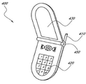
도 9A 는 힌지를 갖는 이동 통신 장치의 한 타입을 나타낸다. 9A illustrates one type of mobile communication device having a hinge.
도 9B 는 상기 이동 통신 장치의 스트린과 상기 이동 통신 장치의 몸체 사이에 전기적인 연결을 제공하는 가요성 회로를 나타낸다. 9B illustrates a flexible circuit that provides an electrical connection between the string of the mobile communication device and the body of the mobile communication device.
II. 교대로 접지된 트레이스에 의한 구리 단층 차폐(Single Copper Layer Shielding With Alternate Grounded Traces) 실시II. Single Copper Layer Shielding With Alternate Grounded Traces
도 1H는 교대로 접지된 트레이스에 의한 구리 단층 차폐(Single Copper Layer Shielding With Alternate Grounded Traces)의 일 실시예를 나타낸다. 도 2는, 차폐된 가요성 회로를 제조하기 위한, 스텝 501-508 을 포함하는 공정도를 나타내며, 도 1A 내지 1H 는 상기 방법의 각각의 단계가 실행됨에 따른 상기 차폐된 가요성 회로의 구조를 나타낸다. 여기서 설명하는 바와 같이, 방법의 각각의 단계에서의 회로의 구조와 연관되어 있는 도면들이 참조될 것이다. 이와는 대조적으로, 도 2의 방법의 각각의 스텝은 도 2 만의 참조 번호를 사용하여 참조될 것이다. 1H illustrates one embodiment of Single Copper Layer Shielding With Alternate Grounded Traces. 2 shows a process diagram comprising steps 501-508 for manufacturing a shielded flexible circuit, and FIGS. 1A-1H show the structure of the shielded flexible circuit as each step of the method is executed. . As described herein, reference will be made to the drawings associated with the structure of the circuit at each step of the method. In contrast, each step of the method of FIG. 2 will be referenced using the reference numerals of FIG. 2 only.
이러한 실시예에서, 차폐된 가요성 회로를 제조하기 위한 방법은 도 1A 에도시된 가요성 지지 부재 100 으로 시작된다. 상기 가요성 지지 부재 100은, 가요성 기판 102와 베이스 전도층 101의 두개의 층으로 구성된다. 당업자들에게 가요성 지지 부재 100은 상업적으로 만들어지며 쉽게 구입이 가능하다고 알려져 있다. 다른 실시예들에서, 상기 방법은, 상기 베이스 전도층 101을 상기 가요성 기판 102 에, 플레이팅, 라미네이팅, 증기 증착(vapor deposition) 또는 알려진 기술들을 사용해서, 부착시키는 것으로 시작된다. In this embodiment, the method for manufacturing a shielded flexible circuit begins with the
바람직한 실시예에서, 상기 가요성 기판 102는 폴리이미드(polyimide)로 만들어진다. 다른 실시예에서, 상기 가요성 기판 102는 일반적으로 사용되는 "FLEX" 또는 FR4, PET/PEN, Teflon/high speed materials 등등의 인쇄회로기판(printed circuit board, "PCB")물질들 중 하나 일 수 있다. In a preferred embodiment, the
바람직한 실시예에서, 상기 베이스 전도층 101 은 구리층이다. 다른 실시예에서, 베이스 전도층 101 은, 금 또는 은과 같은, 전기적으로 전도성 물질일 수 있다. 다른 물질들이 사용될 수 있지만, 여기서 상기 베이스 전도층 101 은 구리 베이스 전도층 101로 불리울 것이다. In a preferred embodiment, the base
전통적인 PCB 제조 방법은 상기 가요성 지지 부재 100에 툴링 홀(tooling holes) 또는 바이아스(vias)를 만들기 위해서 사용될 수 있다. Traditional PCB fabrication methods can be used to make tooling holes or vias in the
도 1B 는 스텝 501 의 완성 후에 형성된 구리 트레이스 111, 112, 113, 114를 나타낸다. 일 실시예에서, 상기 구리 트레이스 111, 112, 113,114 는 인쇄되고, 해당 기술 분야의 당업자에게 잘 알려진 포토리소그래피 기술을 사용해서 에칭된다. 포토리소그래피 기술은, 핫롤 라이네이터(hot roll laminator) 또는 진공 라미네이션 공정(vacuum lamination process)을 사용하여, 에칭 저항성 건조 필름(dry film etch resist)을 상기 베이스 전도층 101 에 라미네이팅하는 것을 필요로 한다. 많은 에칭 저항성 건조 필름(dry film etch resist)층들은 상업적으로 구할 수 있으며, Dupont® 과 같은 회사에 의해서 만들어지고 있다. 몇몇 실시예 에서, 상기 에칭 저항층 건조 필름(dry film etch resist)층의 두께는 0.0007" 내지 0.0020" 이다. 자외선(UV) 에너지와, 포토툴, Mylar®film, 또는 Mylar®glass 와 같은 적절한 도구를 사용하여, 회로 이미지는 에칭 저항층으로 전달된다. UV 에너지에 노출되지 않은 에칭 저항 부분은 그후 패널에서 화학적으로 세정된다. 예를 들어, 탄산칼륨(Potassium Carbonate)을 포함하는 용액이, 현상되지 않은(즉, UV 에너지에 노출되지 않은) 에칭 저항 부분을 세정하기 위해서 사용될 수 있다. 다음으로, 상기 현상된 에칭 저항을 통해서 노출된 상기 구리가 화학적으로 제거된다. 예를 들어, 염화제2구리 에천트(cupric chloride etchant)의 수용액이 구리를 제거하기 위해 사용될 수 있다. 선택적으로, 알칼린-베이스 에천트와 염화제2철 베이스 에천트(ferric chloride-based etchant) 등의 다른 타입의 구리 에천트가 사용될 수 있다. 1B shows copper traces 111, 112, 113, 114 formed after completion of
도 1C는, 트레이스 111, 112, 113, 114를 갖는 가요성 회로 100의 상부에 적층된, 절연성 또는 유전층을 나타낸다. 이 층은 스텝 502 에 의해서, 전기적 쇼트를 방지하고, 트레이스 111, 112, 113, 114를 오염으로부터 보호하기 위해, 방법에 있어서 후에 만들어지는 접지된 차폐(grounded shielding)로부터, 에칭된 트레이스 111, 112, 113, 114를 절연하기 위해서 만들어진다. 어떠한 유전적(dielectric) 또는 비-전도성 절연 물질(non-conductive insulative material)이라도 사용될 수 있다. 예를 들면, 일실시예에서, 유전층 121은 필름의 일 면에 부착된 써멀 세트(thermal set)를 가진 폴리이미드 필름(polyimide film)으로 만들어진다. 이 실시예에서, 상기 폴리이미드 필름(polyimide film)은 두께가 0.0005" 내지 0.0010" 의 범위이고, 부착된 써멀 세트(thermal set)의 두께는 0.0005" 내지 0.0015" 이다. 상기 필름 121은 상기 에칭된 트레이스 111, 112, 113, 114 의 상부에 위치하고, 상기 접착층은 상기 에칭된 트레이스 111, 112, 113, 114와 접한다. 그후, 오토클레이브 또는 진공 프레스를 사용해서, 상기 필름은 상기 가요성 회로 100에 라미네이트된다. 예를 들면, 기압 210 psi, 온도 385 ℉ 에서 60분간 등과 같은 라미네이션 파라미터가 사용될 수 있다. 다른 알려진 기술들은 상기 유전층 121을 상기 가요성 회로 100에 부착시키기 위해 사용될 수 있다. 1C shows an insulating or dielectric layer stacked on top of the
도 1D 는 스텝 503에 의해서 유전층 121에 형성된 채널 131, 133 을 나타낸다. 상기 채널들 131, 133 은 교대 트레이스 111, 113 에 대응하는 위치에서 형성되고, 불연속(discontinuities)을 형성하여, 후에 그들 사이의 트레이스 112를 위한 차폐를 형성한다. 상기 채널 131, 133은, 각각의 트레이스의 길이 방향으로 그 위의 유전층 121을 제거함으로써, 교대로 접지된 트레이스 111, 113을 노출시킨다. 일 실시예에서, 상기 채널들은 레이져 어블레이션 기술(laser ablation techniques)을 사용해서 형성된다. 다른 실시예에서, 다른 공정 기술, 예를 들면, 플라즈마 에칭과 화학적 밀링 등이 사용될 수 있다. 1D shows
다른 실시예에서, 채널들이 대체로 교대의 트레이스에 대응하는 위치에서 형성될 수 있다는 것이 감지된다. 다른 실시예에서, 상기 생성된 채널들 사이에서의 상기 트레이스들은 차폐된다. In another embodiment, it is sensed that the channels may be formed at locations generally corresponding to alternating traces. In another embodiment, the traces between the generated channels are shielded.
다음으로, 몇몇의 실시예에서, 상기 노출된 교대로 접지된 트레이스들 111, 113은 금속화되어(metalized) 트레이스 111, 113을 산화로부터 보호한다. 예를 들 면, 니켈과 금 화합물이 트레이스 111, 113을 금속화(metalize)하기 위해 사용될 수 있다. Next, in some embodiments, the exposed alternating grounded
도 1E 과 도 1F 는, 스텝 504와 505에 의해, 가요성 회로 100의 상부에 형성된 전도성 차폐층 141과 유전층 171을 나타낸다. 상기 전도층 141은 상기 가요성 회로 100에 적용되어, 상기 교대로 접지된 트레이스 111, 113과 전기적으로 연결되도록 된다. 상기 전도층 141은, 상기 교대로 접지된 트레이스 111, 113과 상기 유전층 121 에 부착할 수 있는 어떠한 전도성 물질로도 구성될 수 있다. 적절한 전도층 141 물질에는, 은 베이스 필름(silver based film)과 은 잉크(silver ink)를 포함하지만, 이에 제한되는 것은 아니다. 상기 전도층 141은, 상기 유전층 121 을 가요성 회로 100에 부착하기 위해 사용된 것과 유사한 기술(예를 들면, 라미네이션)을 사용하여, 상기 가요성 회로 100에 적용된다. 다음으로, 유전층 171은 상기 가요성 회로 100 에 적층되어, 상기 전도층 141의 상부에 위치하게 된다. 라미네이션과 같은 기술이 상기 유전층 171을 상기 도전층 141에 부착하기 위해 사용될 수 있다. 적절한 유전층 171 물질에는, 유전층 121을 위해 사용되는 물질들이 포함되지만, 이에 한정되지 않는다. 상기 전도층 141과 유전층 171 은 위에서 설명한 것과 같이,또는 동시에(즉, 스텝 504와 505가 한 스텝으로 행하여) 상기 가요성 회로 100에 부착될 수 있다고 생각된다. 일 실시예에서, 상기 전도층 141과 상기 유전층 171을 동시에 적용하는 것은, 전도층과 유전층으로 구성된 프리-메이드 물질을 사용해서 행하여 질 수 있다. 이러한 물질들의 예로는 Tatsuta's® PC 시리즈를 찾을 수 있다. 이러한 물질들은, 전도성 접착층(conductive adhesive layer) 과 유전층 사이에 샌드위치된, 은 포일의 전도층을 구성한다. 물질들은 상기 가요성 회로 100의 상부에 위치하여, 상기 전도성 접착층이 유전층 121과 접하게 된다. 그후, 상기 물질은 라미네이트 되거나, 아니면 상기 가요성 회로 100에 부착된다. 1E and 1F show the
도 1F 는, 스텝 506에 의해, 상기 가요성 기판 102에서, 상기 가요성 회로 100의 바닥부에 위치하고, 상기 교대로 접지된 트레이스 111, 113의 아래에 형성된, 채널 151, 152 을 나타낸다. 상기 채널 151, 152는 스텝 503에서 적용되는 테크닉과 유사한 기술(예를 들면, 레이져 어블레이션(laser ablation))을 사용하여 만들어진다. 일 실시예에서, 상기 채널들은 상기 가요성 기판 102에 형성되어, 상기 교대로 접지된 트레이스 111, 113이 트레이스의 길이 방향으로 노출된다. 다음으로, 몇몇 실시예에서, 상기 노출된 구리 트레이스 111, 113은 니켈/금 화합물을 사용하여, 산화를 막기 위해 금속화(metalize)된다. FIG. 1F shows the
도 1G 는, 스텝 507에 의해, 상기 가요성 기판 102의 아래 부분에 상기 가요성 회로 100의 사이드에 적층된 상기 전도성 차폐층 161을 나타낸다. 이러한 전도성 차폐층 161은 적층되어 상기 교대로 접지된 트레이스 111, 113과 전기적으로 연결되게 된다. 스텝 508에 대하여 앞에서 설명한 바와 같이, 상기 전도성 차폐층 161 은 상기 가요성 회로 100에 라미네이트 될 수 있으며, 또한, 구리 또는 은과 같은 어떠한 전도성 물질로도 구성될 수 있다. FIG. 1G shows the
도 1H 는, 스텝 508에 의해서, 상기 도전성 차폐층 161에 부착된 유전층 172를 나타낸다. 이러한 유전층 172는 상기 노출된 전도성 차폐층을, 전기적 간 섭(interference)과 오염으로부터 보호한다. 상기 유전층 172 는 상기 가요성 회로 100에, 라미네이션과 같은 기술을 사용해서 부착될 수 있으며, 스텝 502에서 사용되는 것과 유사한 물질(예를 들면, 폴리이미드 필름)로 구성될 수 있다. FIG. 1H shows the
스텝 504와 505에 관해서 설명한 바와 같이, 상기 전도성 차폐층 161과 상기 유전층 172 는, Tatsuta® PC series 를 포함하는 물질들과 같은 물질들을 사용하여, 한 스텝으로, 상기 가요성 회로 100에 적층될 수 있다. As described with respect to
도 1H 에서 보는 바와 같이, 중심 구리 트레이스 112 의 모든 사이드들이 차폐된다. 첫번째로 비-전도성 유전적 물질들에 의해 차폐되고, 이후 상기 비-전도성 물질(non-conductive material)은 전도성 물질들에 의해 둘러싸인다. 특히, 상기 트레이스 112 는, 유전층 121에 의해서, 상부와 사이드에서, 상기 접지면 111, 113, 141 로부터 전기적으로 절연되고, 바닥부에서 가요성 기판 102 에 의해 접지면 161로부터 전기적으로 절연된다. 이 설명에서, 상기 전도성 차폐는, 상기 트레이스 112의 상부 전도층 141, 상기 트레이스 112의 바닥부 전도층 161, 및 상기 트레이스 112의 사이드에서 상기 교대로 접지된 트레이스 111, 113 으로 구성된다. As shown in FIG. 1H, all sides of the
추가적으로, 유전층 171, 172 는, 상기 회로를 EMI 로부터 차폐하는 것이 필요하지 않다. 몇몇 실시예에서, 층 171, 172 중 하나 또는 어느 것도 적용되지 않을 수 있다. In addition,
III. "모든 트레이스가 차폐된 하나의 구리층" 실시예 ("Single Copper Layer With All Traces Shielded" Embodiments)III. "Single Copper Layer With All Traces Shielded" Embodiments
도 3은 모든 트레이스가 차폐된 하나의 구리층의 실시예를 나타낸다. 도 4는 스텝 601 - 608 을 포함하는 도 3에 나타난 차폐된 가요성 회로 900 을 제조하는 하나의 방법에 대한 공정도(a process diagram)를 나타낸다. 여기서 설명한 바와 같이 도 4의 스텝들은 도 4에서 사용된 참조번호로써 나타내어 질 것이다. 3 shows an embodiment of one copper layer with all traces shielded. FIG. 4 shows a process diagram for one method of manufacturing the shielded
도 3과 도 4의 장치의 제조를 위한 장치와 방법은 도 1A-H 와 도 2에서 나타난 실시예의 특징을 공유한다. 다시 말하면, 교대로 접지된 트레이스를 갖는 하나의 구리층에 관해 제안 및/또는 적용된 많은 가능한 물질과 기술은 모든 트레이스들이 차폐된 하나의 구리층 실시예와 연결되어 사용될 수 있다. 그러나, 두가지 세트의 실시예들간의 차이점은 아래와 같다. 3 and 4 share the features of the embodiment shown in FIGS. 1A-H and FIG. 2. In other words, many possible materials and techniques proposed and / or applied with respect to one copper layer having alternately grounded traces can be used in connection with one copper layer embodiment where all traces are shielded. However, the differences between the two sets of embodiments are as follows.
또한, 이 부분에서 설명되고 있는 실시예들에 주어진 타이틀이 제한하는 것으로 생각되어서는 안된다. 모든 트레이스 111, 112가 차폐된 필요는 없는 것으로 생각된다. 그보다는, 이러한 실시예들에서, 모든 트레이스 111, 112를 차폐하는 것은 가능하다. Also, it should not be considered as limiting the title given to the embodiments described in this section. It is believed that not all traces 111 and 112 need to be shielded. Rather, in these embodiments, it is possible to shield all traces 111, 112.
일 실시예에서, 차폐된 가요성 회로 900을 제조하기 위한 방법은 도 1A 에 나타난 부재 100과 같은 가요성 지지 부재로부터 시작된다. 도 3과 도 4를 참조하면, 활성 신호 트레이스 111, 112는 기반 전도층 101로부터, 프린트와 에칭 기술 601을 사용하여 형성된다. 유전층 121은, 스텝 604에서 적층된 차폐 141의 전도성 부분으로부터 트레이스 111, 112를 전기적으로 절연시키기 위해, 그후 트레이스 111, 112의 상부에 적층된다. In one embodiment, a method for manufacturing a shielded
다음으로, 스텝 603에서, 채널 182, 183,184 는 상기 활성 신호 트레이스 111, 112 사이에 형성된다. 상기 채널 182, 183, 184 는, 상기 트레이스 111, 112 사이에 위치한 유전층 121 부분을 제거하기 위해, 레이져 어블레이션 기술(laser ablation techniques)을 사용해서 만들어진다. 도 3에서 설명된 실시예들에서, 트레이스 111, 112 는 채널들을 노출시키지는 않는다. Next, in
결과적으로, 전도성 차폐층 141은, 스텝 604에서, 상기 유전층 121의 상부와 채널 182, 183, 184에 위치한다. 상기 전도성 차폐층 141은 스텝 604에서 상기 가요성 회로 900 의 상부에 부착되어, 가요성 기판 102와 접촉하게 된다. 다음으로, 절연층 171은, 스텝 605에서, 전도성 차폐층의 상부에 부착되게 된다. 스텝 605와 605를 수행하기 위해서, 연결된 스텝 604와 605는 a Tatsuta® PC series material을 사용하여 한번에 수행할 수 있는 것으로 생각되고 있다. As a result, the
제 2 채널 세트 185, 186, 187 은 스텝 606에서 상기 가요성 회로 900의 바닥부에 형성된다. 상기 채널 185, 186, 187은 트레이스 111, 112 사이에 위치하여, 상기 제1 채널 세트 182, 183, 184의 사이에 위치한 상기 전도성 차폐층 141을 노출한다. 상기 제2 채널 세트 185, 186, 187 은, 이러한 위치들에서의 상기 가요성 기판 102의 부분을 제거하기 위해, 레이져 어블레이션 기술(laser ablation techniques)을 적용하여 만들어진다. The second set of
전도성 차폐층 161은 그후 스텝 607에서 상기 가요성 회로 900의 바닥부에, 예를 들면, 라미네이션 기술을 사용하여, 부착된다. 이러한 전도성 차폐층 161은 채널 185, 186, 187에 적층되고, 전도성 차폐층 141과 전기적으로 연결되게 된다. 다음으로, 유전층 199는, 스텝 608에서, 또한 라미네이션 기술을 사용하여, 상기 전도성 차폐층 161에 부착된다. 스텝 604와 605에 대해 설명한 바와 같이, 스텝 607과 608은 차례로 수행되거나, 하나의 스텝으로 수행될 수 있다. The
추가적으로, 몇몇 실시예에서, 유전층 171과 199 중 하나 또는 모두는 전도층 141과 161을 절연하기 위해서 사용되지 않을 것이다. 유전층 171, 188의 부재는 트레이스 111, 112를 EMI로부터 차폐하기 위해 요구되지는 않을 것이다. Additionally, in some embodiments, one or both of
또한, 몇몇 실시예에서, 방법의 스텝 606, 상기 가요성 회로 900의 바닥부의 레이져 어블레이팅 채널(laser ablating channel)185, 186, 187은 생략될 수 있다고 인식된다. 스텝 606을 생략하는 것은, 스텝 603에서, 상기 가요성 지지부재의 상부의 채널 182, 183, 184의 레이져 어블레이션(laser ablation), 유전층 121의 부분과 상기 트레이스 111, 112 사이에 위치한 폴리이미드층 102 모두가 제거되는 것을 요구한다. Further, in some embodiments, it is recognized that
도 3에 나타난 바와 같이, 트레이스 111, 112는, 첫번째로는 유전적 차폐 (dielectric shielding)에 의해, 두번째로는 전도성 차폐(conductive shielding)에 의해 각각 360 도 차폐된다. 각각의 트레이스 111, 112 은 모든 방향에서 상기 전도성 차폐 물질과 다른 트레이스 111, 112 로부터 절연된다. 유전층 121은 상기 트레이스 111, 112의 상부와 사이드를 접지면(the ground plane) 182로부터 전기적으로 절연하고, 가요성 기판 102는 상기 트레이스 111, 112의 바닥부를, 접지 면(the ground plane) 161로부터 전기적으로 절연한다. 따라서, 각각의 트레이스 111, 112는 접지되고 전도성이 있는 차폐 물질로 둘러쌓인다. 전도층 141은, 상기 트레이스 111, 112의 상부와 사이드에 전도성 차폐를 제공하고, 바닥부 전도 층 161은 상기 트레이스 111, 112,113의 바닥부에 전도성 차폐를 제공한다. As shown in FIG. 3, traces 111 and 112 are each shielded 360 degrees, first by dielectric shielding and secondly by conductive shielding. Each
IV,."두 개의 구리층" 실시예 ("Two Copper Layer" Embodiments)IV,. "Two Copper Layer" Embodiments
도 5F 는 두개의 구리층이 차폐된 가요성 회로의 실시예를 나타낸다. 도 6은, 스텝 701 - 706을 포함하는, 도 5F 의 차폐된 가요성 회로를 제조하기 위한, 공정도를 나타내며, 도 5A - F 는 상기 방법의 각각의 스텝이 실행됨에 따라 상기 차폐된 가요성 회로의 구조를 나타낸다. 여기서 설명되는 바와 같이, 방법의 각각의 스텝에서의 상기 회로의 구조와 연결되어 있는 도면들이 참조로서 사용될 것이다. 이와는 대조적으로, 도 6의 공정도의 각각의 스텝은 도 6의 참조 번호를 사용하여 참조될 것이다. 5F shows an embodiment of a flexible circuit with two copper layers shielded. FIG. 6 shows a process diagram for manufacturing the shielded flexible circuit of FIG. 5F, comprising steps 701-706, and FIGS. 5A-F show the shielded flexible circuit as each step of the method is executed. It shows the structure of. As described herein, the figures connected with the structure of the circuit at each step of the method will be used as reference. In contrast, each step of the process diagram of FIG. 6 will be referenced using the reference numerals of FIG. 6.
설명된 실시예에서, 차폐된 가요성 회로의 제조를 위한 방법은 도 5A 에 도시된 지지 부재 200으로부터 시작된다. 상기 가요성 지지부재 200은 3개의 층으로 구성되고, 가요성 기판 202 는 상부 전도층 203과 바닥부 전도층 201 사이에 샌드위치되게 된다. 당업자에게 공지된 바와 같이 가요성 지지부재 200은 상업적으로 만들어지고 쉽게 구매할 수 있다. 다른 실시예에서, 상기 방법은, 플레이팅(plating), 라미네이션, 증기 증착(vapor deposition) 또는 다른 알려진 기술을 사용하여, 상부와 바닥부 전도층 201, 203을 상기 가요성 기판 202에 적층하는 것으로부터 시작된다. 여기서 기술되는 실시예들이, 구리로 구성된 상부와 바닥부 전도층 201, 203에 한정되지는 않으며, 기술된 실시예들은 구리 상부와 바닥부 전도층 201, 203을 활용한다. In the described embodiment, the method for manufacturing the shielded flexible circuit begins with the
또한, 교대로 접지된 트레이스에 의한 구리 단층 차폐에 관해서 제안된 된 많은 대체 물질들과 기술들이, 상기 두개의 구리층 실시예들과 연결되서 사용될 수 있다. 그러나, 이러한 두가지 실시예 세트에서의 차이점들이 이하에서 설명된다. In addition, many alternative materials and techniques proposed with respect to copper single layer shielding by alternating grounded traces can be used in conjunction with the two copper layer embodiments. However, the differences in these two sets of embodiments are described below.
도 5B 는, 스텝 701에서, 상부 구리층 203으로부터 프린트되거나 에칭된 후의 트레이스 211, 212, 213, 214를 나타낸다. 보는 바와 같이, 트레이스 211, 212, 213, 214 는, 도시된 실시예의 디자인 요구사항이 상기 트레이스 211, 212, 213, 214 가 서로 전기적으로 분리되어 있을 것을 요구하기 때문에, 서로 전기적으로 연결되어 있지 않다. 5B shows
도 5C 는, 스텝 702에서, 상기 가요성 회로 200 의 상부에 적층된 절연층 또는 유전층 221을 나타낸다. 예를 들면, 라미네이션 기술을 사용하여, 유전층 221은 상기 가요성 기판 202 과 상기 트레이스 211, 212, 213, 214 에 적층된다. 5C shows an insulating layer or
도 5D 는, 스텝 703에서 활성 신호 트레이스 211, 212, 213, 214 사이에 만들어지는 채널 231, 232, 233, 234 을 나타낸다. 상기 채널 231, 232, 233, 234 는 상기 유전층 221의 부분과 상기 트레이스 211, 212, 213, 214 사이에 위치한 상기 가요성 기판 202을 제거하기 위해, 레이져 어블레이션(laser ablation) 또는 알려진 다른 기술들을 적용하여 만들어진다. 도시된 바와 같이 상기 채널 231, 232, 233, 234는 바닥부 구리층 201의 상부를 노출하지만, 상기 트레이스 211, 212, 213, 214를 노출하지는 않는다.(즉, 트레이스 211, 212, 213, 214는 절연되어 있다. 5D shows
도 5E 는, 스텝 704에서, 상기 가요성 회로 200의 상부에 적층된 전도성 차폐층 241 을 나타낸다. 상기 전도성 차폐층 241은, 상기 가요성 회로 240에 적층되어, 상기 채널 231, 232, 233, 234에 위치하게 하며, 바닥부 전도층 201과 전기적으로 연결되게 된다. 일 실시예에서, 상기 전도성 차폐층 241은 은이 채워진 잉크이다. Dupont's® CB208 product 는 은 잉크(silver ink)이며 상업적으로 이용가능하고 당업자에게 알려져 있다. 전형적으로 은 잉크(silver ink)는, 바닥부 전도층 201을 노출시키기 위해 미리 레이저 처리된 상기 유전층 221의 표면에 스크린 프린트된다. 다른 실시예에서, 요구되는 흐름 특성the requisite flow characteristics을 갖는 다른 전도성 물질이 사용될 수 있다. FIG. 5E shows the
도 5F 는, 스텝 705와 706에서, 상기 가요성 회로 200의 상부와 바닥부에 적층된 절연성 또는 유전층 251, 252를 도시한다. 몇몇 실시예에서, 유전 필름 251, 252는 상기 가요성 회로 200에 라미네이트 된다. 상기 유전층 251, 252는 상기 가요성 회로 250을 외부적 쇼팅(external shorting)으로부터 보호하는 것으로 작용할 수 있다. FIG. 5F shows insulating or dielectric layers 251, 252 stacked on top and bottom of the
다른 실시예에서, 스텝 704는 라미네이팅 또는 전도성 필름을 상기 유전층과 상기 채널 231, 232, 233, 234에 부착하는 다른 방법으로 행하여 진다. 이러한 실시예들에서, 절연층 252는 그후, 외부적 쇼팅(external shorting)을 방지하기 위 해, 상기 절연성 차폐층 251의 상부에 부착될 수 있다. 선택적으로, 상기 전도성 차폐층 241과 상기 유전층 252 는, 동시에 Tatsuta® PC series와 같은 접착 물질에 의하여, 상기 가요성 회로 250에 적층할 수 있다. In another embodiment,
도 5F에 나타난 바와 같이, 상기 트레이스 211, 212, 213은 360도 차폐된다. 각각의 트레이스 211, 212, 213은 모든 방향에서 상기 전도성 차폐물질과 다른 트레이스 211, 212, 213으로부터 절연된다. 유전층 221은 상기 트레이스 211의 상부와 사이드를, 접지면(grounded plane) 241, 212, 213으로부터 절연하고, 상기 가요성 기판 202는 상기 트레이스 211, 212, 213의 바닥부를 접지면(grounded plane) 201로부터 절연한다. 따라서, 각각의 트레이스 211, 212, 213은 접지된 차폐 물질로 둘러싸이게 된다. 전도층 241은, 상기 트레이스 211, 212, 213의 상부와 사이드부에 전도성 차폐를 제공하고, 상기 바닥 전도층 201은 상기 트레이스 211, 212, 213의 바닥부에 전도성 차폐를 제공한다. As shown in Figure 5F, the
V. "세개의 구리층" 실시예 ("Three Copper Layer" Embodiments)V. "Three Copper Layer" Embodiments
도 7G는 세개의 구리층이 차폐된 가요성 회로의 일 실시예를 나타낸다. 도 8은, 스텝 801-808을 포함하는, 차폐된 가요성 회로의 제조를 위한 방법의 일 실시예를 위한 공정도를 나타내며, 도 7A-G 는 방법의 각각의 스텝이 실행됨에 따라 상기 차폐 가요성 회로의 구조를 나타낸다. 여기서 기술된 것과 같이, 도면들은 방법의 각각의 스텝에서의 회로의 구조와 연관되어 있는 도면들이 참조되었다. 이 와는 대조적으로 도 8의 공정도의 각각의 스텝들은 도 8 에서만의 참조 번호를 사용하여 참조될 것이다. 7G illustrates one embodiment of a flexible circuit with three copper layers shielded. 8 shows a process diagram for one embodiment of a method for manufacturing a shielded flexible circuit, comprising steps 801-808, and FIGS. 7A-G illustrate the shielding flexibility as each step of the method is executed. The structure of the circuit is shown. As described herein, the figures are referred to figures associated with the structure of the circuit at each step of the method. In contrast to this, each step of the process diagram of FIG. 8 will be referred to using a reference numeral only in FIG. 8.
일 실시예에서, 차폐된 가요성 회로를 제조하기 위한 방법은 도 7A 에 도시된 가요성 지지부재 300 으로부터 시작된다. 상기 가요성 지지부재 300은 3개의 구리층으로 구성되며, 가요성 기판 302는, 상부 전도층 303과 바닥부 전도층 301 사이에 샌드위치 된다. 가요성 지지부재 300이 상업적으로 제조되고 쉽게 구입할 수 있다는 것은 당업자들에게 알려져 있다. 다른 실시예에서, 상기 방법은, 플레이팅, 라미네이션, 증기 증착 또는 다른 알려진 기술을 사용하여, 상기 상부와 바닥부 베이스 전도층을 상기 가요성 기판에 적층하는 것으로부터 시작된다. 또 다른 실시예에서, 상기 상부와 바닥부 전도층은, 구리, 은, 또는 금과 같은 어떠한 전도성 물질로도 구성될 수 있다. In one embodiment, a method for manufacturing a shielded flexible circuit begins with the
도 7B 는, 스텝 801에서, 프린트 되고 에칭된 후에, 전기적 신호를 전달하기 위해 사용된 트레이스 311, 312, 313, 314를 도시한다. 상기 트레이스 311, 312, 313, 314는 상부 전도층 303 으로부터 에칭된다. FIG. 7B shows
도 7C 는, 스텝 802와 803 가 완료된 후의 상기 가요성 회로 300 을 도시한다. 스텝 802는, 유전성 물질 321 을 상기 가요성 회로 300의 상부에 적층하는 것을 요구한다. 상기 유전층 322는 앞서 개시된 전기적으로 절연성이 있는 어떠한 물질로도 구성될 수 있으며, 앞서 설명된 어떠한 기술을 사용하여 상기 가요성 회로에 적층될 수 있다. 스텝 803은 전도성 차폐층 322을, 유전층 321의 상부에 적층하는 것을 필요로 한다. 일 실시예에서, 상기 전도성 차폐층 322 는 구리 호 일(copper foil)이다. 상기 구리 호일은, 라미네이션 기술 또는 다른 당업계에 알려진 기술을 사용하여, 상기 가요성 회로 300에 부착된다. 7C shows the
다른 실시예에서, 스텝 802와 803은, 전도층과 유전층을 구성하는 물질을 사용하여 동시에 진행될 수 있다. 상기 물질들은, 상기 트레이스 311, 312, 313, 314와 물리적으로 접촉하고 있는 유전층을 가진 상기 가요성 회로 300에 부착된다. 다른 실시예에서, 스텝 802와 803은, 유전적 접착제(dielectric adhesive)로 상기 가요성 회로 300에 접착하고 있는 전도성 물질을 사용하여 동시에 진행될 수 있다. 이러한 실시예에서, 상기 전도성 물질은 구리 호일이고, ADH/PI/ADH 와 같은 유전 호일 결합 접착제(dielectric foil bonding adhesives)가 사용될 수 있다. In another embodiment, steps 802 and 803 may proceed simultaneously using the materials that make up the conductive and dielectric layers. The materials are attached to the
도 7D 는, 스텝 804에서, 상기 트레이스 311, 312, 313, 314 사이에 형성된 채널 331, 332, 333, 334 를 도시한다. 상기 채널 331, 332, 333, 334 는, 상기 트레이스 311, 312, 313, 314 사이에 위치한 상기 가요성 기판 302, 상기 유전층 321, 및 상기 전도성층 322 부분을 제거하여 생성된다. 상기 채널 331, 332, 333, 334는 상기 바닥부 전도층 301을 노출시킬 수 있을 정도의 충분한 깊이이다. 위에서 설명한 바와 같이, 레이저 어블레이션(laser ablation)과 같은 기술이 상기 채널 331, 332, 333, 334 를 만들기 위해 사용될 수 있다. FIG. 7D shows the
도 7E 는, 스텝 805에서, 상기 채널 331, 332, 333, 334에 적층된 구리 플레이팅 341, 342, 343, 344 을 나타낸다. 상기 구리 플레이팅은 상기 전도성 차폐층 322와 바닥부 전도층 301 사이의 전기적 연결을 제공한다. 상기 채널 341, 342, 343, 344 에 구리를 플레이트하기 위해서, SHADOW® process 와 같은 일반적인 방법들이 사용될 수 있다. SHADOW® 은, 구리 플레이트 공정을 촉진하는 흑연을 기반으로 직접 금속화(matallization)하는 프로세스이다. FIG. 7E shows the copper plating 341, 342, 343, 344 laminated to the
몇몇 실시예에서, 구리 플레이팅에 사용된 바로 그 기술과 물질들이, 상기 전도성 차폐층 322 와 바닥부 전도층 301을 전기적으로 연결시키기 위해 사용된다. 이러한 기술과 물질들은, 스크리닝 기술을 사용해서 은 잉크(silver ink)를 적용하는 것을 포함할 수 있다. In some embodiments, the very techniques and materials used for copper plating are used to electrically connect the
상기 전도성 차폐층 322와 상기 바닥부 전도층 301 사이에 전기적 연결이 형성된 후, 필요없는 구리들은, 스텝 806에서, 포토리소그래피와 같은 잘 알려진 기술을 사용해서, 상기 가요성 회로 300 으로부터 제거된다. 예를 들면, 전도성 차폐층 322의 상부에 우연히 놓여지게 된 구리들은 스텝 806에서 제거된다. After the electrical connection is made between the
도 7F 는, 스텝 807에서, 상기 전도성 차폐층 322의 상부에 적층된 유전층 351과 플레이트된 채널 341, 342, 343, 344 를 나타낸다. 도 7G 는, 스텝 808 에서, 상기 바닥부 전도층 301의 바닥부에 적층된 유전층 352 를 나타낸다. 유전층 351, 352 는 상기 가요성 회로 350 을 외부 쇼팅(external shorting) 으로부터 보호할 수 있다. 그러나, 위에서 말한 바와 같이, 몇몇 실시예들은 단지 하나의 유전층 351, 352 을 적용하거나 또는 유전층을 적용하지 않는다. FIG. 7F shows, in
도 7G 에 나타난 바와 같이, 상기 트레이스 311, 312, 313 은 360 도 차폐된다. 각각의 트레이스 311, 312, 313 은 상기 전도성 차폐 물질과 다른 트레이스 311, 312, 313 로부터 모든 방향에서 절연된다. 유전층 321은, 접지면(grounded plane) 322, 341, 342, 343, 344으로부터 상기 트레이스 311, 312, 313 의 상부와 사이드를 전기적으로 절연한다. 따라서, 각각의 트레이스 311, 312, 313 은 접지된 차폐 물질들로 둘어싸여 있다. 전도층 322는 상부 접지된 차폐 물질(top grounded shielding material)이며, 바닥부 전도층 301은 바닥부 차폐 물질이다. 상기 플레이트된 채널 341, 342, 343, 344는 상기 트레이스 311, 312, 313의 사이드들을 차폐하고, 전도층 322와 바닥부 전도층 301을 전기적으로 연결한다. As shown in FIG. 7G, the
VI. 적용예(application Example)VI. Application Example
여기서 개시된 상기 차폐된 가요성 회로를 제조하는 장치와 방법은, 일예로 플립폰에 적용될 수 있다. 도 9A 는 플립폰 400의 하나의 타입을 나타낸다. 전형적인 플립폰 400은, 몸체 420, 스크린 430과 안테나 410 으로 구성된다. 상기 몸체 420 은, 힌지 450을 통해서 상기 스크린 430에 기계적으로 연결된다. 상기 몸체 420 은, 전송되어 안테나 410 로 수신된 데이타를 처리하는 회로소자로 구성된다. 따라서 전송되어 수신된 데이타에 상응하는 이미지들이 스크린 430에 디스플레이된다. Apparatus and methods for manufacturing the shielded flexible circuits disclosed herein may be applied to flip phones, for example. 9A shows one type of
도 9B 는, 몸체 420이 스크린 430으로부터 물리적으로 분리된 후의 플립폰 400을 도시한다. 보는 바와 같이, 여기서 개시된 제조 장치 및 방법에 따른 차폐된 가요성 회로 440 은 상기 몸체 420과 상기 스크린 430 사이의 전기적 연결을 제공한다. 상기 차폐된 가요성 회로 440 은, 상기 힌지의 회전축 450 을 따라 기계 적으로 가요성이 있어야 한다. 이러한 가요성은 상기 플립폰 400 을 열고 닫기 위해서 필요하다. 더구나, 스트리밍 비디오(streaming video)와 같은 용도를 위해 요구되는 높은 데이타 전송 속도 때문에, 상기 차폐된 가요성 회로 440 에서의 상기 트레이스는, 각각의 트레이스들을 외부 소스(external source)로부터 만들어진 EMI 와 상기 가요성 회로 400의 다른 트레이스로부터 차폐할 수 있어야 한다. 따라서, 상기 차폐된 가요성 회로 440 은, 상기 플립폰 400 에서, 유리하게 상기 몸체 420 과 상기 스크린 430 사이의 전기적 연결을 제공할 수 있다. 9B shows the
실시예에서는, 상기 차폐된 가요성 회로 440의 일 실시예는 EMI 에 따른 실질적인 신호의 손실이나 일그러짐 없이, 데이타 전송 속도를, 2 내지 4 GHz 사이에서 조정할 수 있다. 또한, 이러한 실시예에서, 근접한 트레이스들의 중심간의 거리는 1 인치의 2만분의 1 정도로 작을 수 있다. In an embodiment, one embodiment of the shielded
VII. 결론 (Conclusion)VII. Conclusion
앞에서 상기 차폐된 가요성 회로의 제조를 위한 장치와 방법들을 위한 실시예들을, 본 발명이 속하는 기술 분야의 당업자가, 이러한 구성요소를 생산하고, 이러한 방법들을 실시할 수 있도록, 자세하고, 분명하며, 정확한 용어로 설명하였다. 이러한 장치과 방법은, 그러나, 앞에서 논의된 실시예들과 완전히 일치하는 변형의 여지가 있다. 결과적으로, 이러한 장치들과 방법들은 개시된 특별한 실시예들에 한정되지 않는다. 그와는 반대로, 이러한 장치들과 방법들은 본 발명의 정신과 범 위 내에서 모든 변형들을 커버한다. The embodiments for apparatuses and methods for the fabrication of the shielded flexible circuits described above are detailed, clear and detailed so that those skilled in the art can produce such components and implement these methods. , Explained in exact terms. Such devices and methods, however, are subject to variations that are in full agreement with the embodiments discussed above. As a result, these devices and methods are not limited to the particular embodiments disclosed. On the contrary, these devices and methods cover all modifications within the spirit and scope of the invention.
Claims (38)
Applications Claiming Priority (6)
| Application Number | Priority Date | Filing Date | Title |
|---|---|---|---|
| US79671606P | 2006-05-02 | 2006-05-02 | |
| US60/796,716 | 2006-05-02 | ||
| US81192706P | 2006-06-08 | 2006-06-08 | |
| US60/811,927 | 2006-06-08 | ||
| US11/739,550 | 2007-04-24 | ||
| US11/739,550 US7645941B2 (en) | 2006-05-02 | 2007-04-24 | Shielded flexible circuits and methods for manufacturing same |
Publications (1)
| Publication Number | Publication Date |
|---|---|
| KR20090008405A true KR20090008405A (en) | 2009-01-21 |
Family
ID=38694381
Family Applications (1)
| Application Number | Title | Priority Date | Filing Date |
|---|---|---|---|
| KR1020087028721A KR20090008405A (en) | 2006-05-02 | 2007-04-26 | Shielded flexible circuits and methods for manufacturing same |
Country Status (5)
| Country | Link |
|---|---|
| US (2) | US7645941B2 (en) |
| JP (1) | JP2009535848A (en) |
| KR (1) | KR20090008405A (en) |
| HK (1) | HK1131718A1 (en) |
| WO (1) | WO2007133405A2 (en) |
Cited By (2)
| Publication number | Priority date | Publication date | Assignee | Title |
|---|---|---|---|---|
| KR20170132931A (en) * | 2016-05-24 | 2017-12-05 | 엘지디스플레이 주식회사 | Cable and rollable flexible display device |
| WO2023075141A1 (en) * | 2021-10-27 | 2023-05-04 | 삼성전자 주식회사 | Electronic device comprising rf cable |
Families Citing this family (22)
| Publication number | Priority date | Publication date | Assignee | Title |
|---|---|---|---|---|
| US20090040191A1 (en) * | 2007-08-08 | 2009-02-12 | Synaptics Incorporated | Capacitive touch sensor with conductive trace lines in bonding region |
| DE102007044602A1 (en) * | 2007-09-19 | 2009-04-23 | Continental Automotive Gmbh | Multilayer printed circuit board and use of a multilayer printed circuit board |
| US9723709B2 (en) * | 2007-10-22 | 2017-08-01 | Todd Steigerwald | Method for assigning control channels |
| US8028406B2 (en) * | 2008-04-03 | 2011-10-04 | International Business Machines Corporation | Methods of fabricating coplanar waveguide structures |
| US8456851B2 (en) * | 2008-05-16 | 2013-06-04 | Apple Inc. | Flex circuit with single sided routing and double sided attach |
| KR20100104911A (en) * | 2009-03-19 | 2010-09-29 | 삼성전자주식회사 | Semiconductor package |
| TWI387407B (en) * | 2009-06-10 | 2013-02-21 | Htc Corp | Flexible printed circuit and fabrication method thereof |
| CN101932188B (en) * | 2009-06-18 | 2013-05-08 | 宏达国际电子股份有限公司 | Flexible printed circuit board and composition method thereof |
| US20110024160A1 (en) * | 2009-07-31 | 2011-02-03 | Clifton Quan | Multi-layer microwave corrugated printed circuit board and method |
| US8362856B2 (en) * | 2009-11-17 | 2013-01-29 | Raytheon Company | RF transition with 3-dimensional molded RF structure |
| US9072164B2 (en) * | 2009-11-17 | 2015-06-30 | Raytheon Company | Process for fabricating a three dimensional molded feed structure |
| US8127432B2 (en) | 2009-11-17 | 2012-03-06 | Raytheon Company | Process for fabricating an origami formed antenna radiating structure |
| KR101301105B1 (en) * | 2011-11-02 | 2013-08-27 | 포항공과대학교 산학협력단 | Transmission Line For Ship |
| JP2013187248A (en) * | 2012-03-06 | 2013-09-19 | Nec Computertechno Ltd | Dielectric film, printed circuit board and characteristic impedance adjustment method |
| US9799426B2 (en) | 2012-11-08 | 2017-10-24 | 3M Innovative Properties Company | Ribbed high density electrical cable |
| KR101705973B1 (en) * | 2015-04-22 | 2017-02-13 | 연세대학교 산학협력단 | Electromagnetic wave shileding dielectric film |
| CN106376169A (en) * | 2015-07-24 | 2017-02-01 | 宏启胜精密电子(秦皇岛)有限公司 | Circuit board and manufacturing method thereof |
| JP7390779B2 (en) * | 2017-04-28 | 2023-12-04 | 日東電工株式会社 | Flexible wiring circuit board and imaging device |
| CN111972051A (en) * | 2018-03-16 | 2020-11-20 | 华为技术有限公司 | Assembly and method for electromagnetic interference shielding |
| WO2020008729A1 (en) * | 2018-07-06 | 2020-01-09 | 天竜精機株式会社 | Transmission line, transmission line manufacturing method and transmission line manufacturing apparatus |
| EP3837503B1 (en) | 2018-08-16 | 2023-08-09 | Micro Motion, Inc. | Electromagnetic interference resistant electronics enclosure |
| CN113973420A (en) * | 2020-07-22 | 2022-01-25 | 庆鼎精密电子(淮安)有限公司 | Rigid-flex board and manufacturing method thereof |
Family Cites Families (65)
| Publication number | Priority date | Publication date | Assignee | Title |
|---|---|---|---|---|
| US3372358A (en) | 1966-04-12 | 1968-03-05 | Itt | Film transformers |
| FR1541719A (en) | 1967-07-17 | 1968-10-11 | Csf | integrated magnetic elements with a laminated structure |
| US3898595A (en) | 1970-11-02 | 1975-08-05 | Cunningham Corp | Magnetic printed circuit |
| BE785906A (en) | 1971-07-12 | 1973-01-08 | High Voltage Power Corp | ELECTROMAGNETIC INDUCTION DEVICE |
| BE862654A (en) | 1977-01-13 | 1978-07-05 | Cit Alcatel | INDUCTIVE CIRCUITS REALIZATION PROCESS |
| US4172245A (en) | 1977-09-06 | 1979-10-23 | Rte Corporation | Adjustable transformer |
| JPS55110009A (en) | 1979-02-16 | 1980-08-25 | Tohoku Metal Ind Ltd | Inductance element |
| US4383235A (en) | 1979-07-30 | 1983-05-10 | Layton Wilbur T | Bi level etched magnetic coil |
| DE3165884D1 (en) | 1980-02-01 | 1984-10-18 | Hasler Ag | Pulse transformer and its use as isolation transformer |
| US4547705A (en) | 1982-03-20 | 1985-10-15 | Tdk Corporation | Discharge lamp lightening device |
| US4622627A (en) | 1984-02-16 | 1986-11-11 | Theta-J Corporation | Switching electrical power supply utilizing miniature inductors integrally in a PCB |
| US4665357A (en) | 1984-04-23 | 1987-05-12 | Edward Herbert | Flat matrix transformer |
| US4901048A (en) | 1985-06-10 | 1990-02-13 | Williamson Windings Inc. | Magnetic core multiple tap or windings devices |
| US4799119A (en) | 1986-09-10 | 1989-01-17 | International Business Machines Corporation | Flexible circuit magnetic core winding for a core member |
| JPS63228604A (en) | 1987-03-18 | 1988-09-22 | Hitachi Ltd | High frequency transformer |
| US4800461A (en) | 1987-11-02 | 1989-01-24 | Teledyne Industries, Inc. | Multilayer combined rigid and flex printed circuits |
| US5070317A (en) | 1989-01-17 | 1991-12-03 | Bhagat Jayant K | Miniature inductor for integrated circuits and devices |
| US5177460A (en) | 1990-01-04 | 1993-01-05 | Dhyanchand P John | Summing transformer for star-delta inverter having a single secondary winding for each group of primary windings |
| JPH03276604A (en) | 1990-03-27 | 1991-12-06 | Toshiba Corp | Plane inductor |
| US5126714A (en) | 1990-12-20 | 1992-06-30 | The United States Of America As Represented By The Secretary Of The Navy | Integrated circuit transformer |
| US5349743A (en) | 1991-05-02 | 1994-09-27 | At&T Bell Laboratories | Method of making a multilayer monolithic magnet component |
| US5487214A (en) | 1991-07-10 | 1996-01-30 | International Business Machines Corp. | Method of making a monolithic magnetic device with printed circuit interconnections |
| GB2263582B (en) | 1992-01-21 | 1995-11-01 | Dale Electronics | Laser-formed electrical component and method for making same |
| US5257000A (en) | 1992-02-14 | 1993-10-26 | At&T Bell Laboratories | Circuit elements dependent on core inductance and fabrication thereof |
| JPH065448A (en) | 1992-06-22 | 1994-01-14 | Matsushita Electric Ind Co Ltd | Choke coil and power source |
| US5312674A (en) | 1992-07-31 | 1994-05-17 | Hughes Aircraft Company | Low-temperature-cofired-ceramic (LTCC) tape structures including cofired ferromagnetic elements, drop-in components and multi-layer transformer |
| US5392020A (en) | 1992-12-14 | 1995-02-21 | Chang; Kern K. N. | Flexible transformer apparatus particularly adapted for high voltage operation |
| JPH0722241A (en) | 1993-07-05 | 1995-01-24 | Matsushita Electric Ind Co Ltd | Planar inductor and production thereof |
| US5514337A (en) | 1994-01-11 | 1996-05-07 | American Research Corporation Of Virginia | Chemical sensor using eddy current or resonant electromagnetic circuit detection |
| US5481238A (en) | 1994-04-19 | 1996-01-02 | Argus Technologies Ltd. | Compound inductors for use in switching regulators |
| JPH07297055A (en) | 1994-04-26 | 1995-11-10 | Matsushita Electric Ind Co Ltd | Choke coil |
| TW265450B (en) | 1994-06-30 | 1995-12-11 | At & T Corp | Devices using metallized magnetic substrates |
| WO1996025752A1 (en) | 1995-02-15 | 1996-08-22 | Electronic Craftsmen Limited | Transformer and method of assembly |
| US5781091A (en) | 1995-07-24 | 1998-07-14 | Autosplice Systems Inc. | Electronic inductive device and method for manufacturing |
| JPH0983104A (en) | 1995-09-12 | 1997-03-28 | Murata Mfg Co Ltd | Circuit board with built-in coil |
| KR100211814B1 (en) | 1995-11-30 | 1999-08-02 | 전주범 | A pliability coil winding structure of fbt and manufacture method therefore |
| US5852870A (en) | 1996-04-24 | 1998-12-29 | Amkor Technology, Inc. | Method of making grid array assembly |
| US5793272A (en) | 1996-08-23 | 1998-08-11 | International Business Machines Corporation | Integrated circuit toroidal inductor |
| US5942965A (en) | 1996-09-13 | 1999-08-24 | Murata Manufacturing Co., Ltd. | Multilayer substrate |
| US6073339A (en) | 1996-09-20 | 2000-06-13 | Tdk Corporation Of America | Method of making low profile pin-less planar magnetic devices |
| DE19639881C2 (en) | 1996-09-27 | 1999-05-20 | Siemens Matsushita Components | Method of manufacturing an inductive component |
| JPH10116746A (en) | 1996-10-09 | 1998-05-06 | Kokusai Electric Co Ltd | Manufacture of thin-film inductor element |
| JP4030028B2 (en) | 1996-12-26 | 2008-01-09 | シチズン電子株式会社 | SMD type circuit device and manufacturing method thereof |
| US5898991A (en) | 1997-01-16 | 1999-05-04 | International Business Machines Corporation | Methods of fabrication of coaxial vias and magnetic devices |
| FI971180A (en) | 1997-03-20 | 1998-12-23 | Micronas Oy | Stripe-line inductor |
| US6353189B1 (en) * | 1997-04-16 | 2002-03-05 | Kabushiki Kaisha Toshiba | Wiring board, wiring board fabrication method, and semiconductor package |
| JPH1140915A (en) | 1997-05-22 | 1999-02-12 | Nec Corp | Printed wiring board |
| WO1998054735A1 (en) | 1997-05-27 | 1998-12-03 | Melcher Ag | Device and method for cooling a planar inductor |
| US6007758A (en) | 1998-02-10 | 1999-12-28 | Lucent Technologies Inc. | Process for forming device comprising metallized magnetic substrates |
| JPH11243016A (en) | 1998-02-25 | 1999-09-07 | Nissha Printing Co Ltd | Manufacture of printed circuit board having printed coil, printed coil sheet, and printed coil chip |
| US6144276A (en) | 1998-04-02 | 2000-11-07 | Motorola, Inc. | Planar transformer having integrated cooling features |
| US6129579A (en) | 1998-06-15 | 2000-10-10 | Segate Technology Inc. | Low inductance flex-to-PCB spring connector for a disc drive |
| US6593836B1 (en) | 1998-10-20 | 2003-07-15 | Vlt Corporation | Bobbins, transformers, magnetic components, and methods |
| JP2000182851A (en) | 1998-12-15 | 2000-06-30 | Matsushita Electric Ind Co Ltd | Inductor |
| JP2000269632A (en) * | 1999-03-17 | 2000-09-29 | Tatsuta Electric Wire & Cable Co Ltd | Shield flexible printed wiring board, manufacture thereof and reinforcing shield film therefor |
| US6040753A (en) | 1999-04-06 | 2000-03-21 | Lockheed Martin Corp. | Ultra-low-profile tube-type magnetics |
| US6211767B1 (en) | 1999-05-21 | 2001-04-03 | Rompower Inc. | High power planar transformer |
| US6262463B1 (en) | 1999-07-08 | 2001-07-17 | Integrated Micromachines, Inc. | Micromachined acceleration activated mechanical switch and electromagnetic sensor |
| TW432412B (en) | 1999-11-15 | 2001-05-01 | Compeq Mfg Co Ltd | Method for fabricating built-in printed circuit board inductor and transformer |
| CN1240086C (en) | 2000-05-19 | 2006-02-01 | P·A·哈丁 | Slot core transformers |
| AU2001294646A1 (en) | 2000-09-22 | 2002-04-02 | M-Flex Multi-Fineline Electronix, Inc. | Electronic transformer/inductor devices and methods for making same |
| AU2001296724A1 (en) | 2000-10-10 | 2002-04-22 | Primarion, Inc. | Microelectronic magnetic structure, device including the structure, and methods of forming the structure and device |
| US6383033B1 (en) | 2000-12-07 | 2002-05-07 | Delphi Technologies, Inc. | Side load electrical connector |
| US6674335B1 (en) | 2002-06-28 | 2004-01-06 | Qualcomm Incorporated | Blind linearization using cross-modulation |
| US7135952B2 (en) | 2002-09-16 | 2006-11-14 | Multi-Fineline Electronix, Inc. | Electronic transformer/inductor devices and methods for making same |
-
2007
- 2007-04-24 US US11/739,550 patent/US7645941B2/en active Active
- 2007-04-26 JP JP2009509606A patent/JP2009535848A/en active Pending
- 2007-04-26 KR KR1020087028721A patent/KR20090008405A/en not_active Application Discontinuation
- 2007-04-26 WO PCT/US2007/010009 patent/WO2007133405A2/en active Application Filing
-
2009
- 2009-10-26 HK HK09109875.2A patent/HK1131718A1/en unknown
- 2009-12-04 US US12/631,532 patent/US20100071935A1/en not_active Abandoned
Cited By (2)
| Publication number | Priority date | Publication date | Assignee | Title |
|---|---|---|---|---|
| KR20170132931A (en) * | 2016-05-24 | 2017-12-05 | 엘지디스플레이 주식회사 | Cable and rollable flexible display device |
| WO2023075141A1 (en) * | 2021-10-27 | 2023-05-04 | 삼성전자 주식회사 | Electronic device comprising rf cable |
Also Published As
| Publication number | Publication date |
|---|---|
| US20080202807A1 (en) | 2008-08-28 |
| WO2007133405A3 (en) | 2008-12-11 |
| US7645941B2 (en) | 2010-01-12 |
| US20100071935A1 (en) | 2010-03-25 |
| WO2007133405A2 (en) | 2007-11-22 |
| JP2009535848A (en) | 2009-10-01 |
| HK1131718A1 (en) | 2010-01-29 |
Similar Documents
| Publication | Publication Date | Title |
|---|---|---|
| US7645941B2 (en) | Shielded flexible circuits and methods for manufacturing same | |
| US7196273B2 (en) | Flat cable, flat cable sheet, and flat cable sheet producing method | |
| TWI458398B (en) | Shielded flexible circuits and methods for manufacturing same | |
| CN102316664B (en) | Flexible circuit board and manufacture method thereof | |
| US8982582B2 (en) | Electronic device with antenna cable bracket | |
| JP2009535848A5 (en) | ||
| JP2007234500A (en) | High-speed transmission fpc and printed circuit board to be connected to the fpc | |
| CN109219232B (en) | Circuit board having electromagnetic wave shielding function, method for manufacturing the same, and flat cable | |
| JP4414365B2 (en) | High-speed transmission board | |
| EP3449532A1 (en) | Component carrier with integrated antenna arrangement, electronic apparatus, radio communication method | |
| JP5081985B2 (en) | Cable connectors and antenna components | |
| US20230019563A1 (en) | High-frequency circuit | |
| EP2410826B1 (en) | Flexible printed circuit board with waterproof structure | |
| US20140166350A1 (en) | Methods for Forming Metallized Dielectric Structures | |
| CN114144945A (en) | Flexible cable | |
| KR20180080612A (en) | Flexible printed circuit board | |
| KR102363957B1 (en) | Cable module and manufacturing method of the same | |
| JP4907281B2 (en) | Flexible printed circuit board | |
| KR20130120101A (en) | Transmission cable, patable device including the same and method for manufacturing same | |
| CN212259433U (en) | High-frequency high-speed circuit board | |
| CN216055120U (en) | Coupling piece based on metal cover | |
| CN212910183U (en) | Flexible circuit board suitable for 5G signal transmission | |
| JP2004179381A (en) | Printed wiring board and its manufacturing method | |
| KR101924579B1 (en) | Stacked cable | |
| JP6333217B2 (en) | Method for producing hollow film cable |
Legal Events
| Date | Code | Title | Description |
|---|---|---|---|
| WITN | Application deemed withdrawn, e.g. because no request for examination was filed or no examination fee was paid |