KR20080098479A - Method of manufacturing magnetoresistive effect element - Google Patents
Method of manufacturing magnetoresistive effect elementInfo
- Publication number
- KR20080098479A KR20080098479A KR1020080104637A KR20080104637A KR20080098479A KR 20080098479 A KR20080098479 A KR 20080098479A KR 1020080104637 A KR1020080104637 A KR 1020080104637A KR 20080104637 A KR20080104637 A KR 20080104637A KR 20080098479 A KR20080098479 A KR 20080098479A
- Authority
- KR
- South Korea
- Prior art keywords
- layer
- functional layer
- magnetization
- functional
- magnetoresistive element
- Prior art date
- Legal status (The legal status is an assumption and is not a legal conclusion. Google has not performed a legal analysis and makes no representation as to the accuracy of the status listed.)
- Granted
Links
Images


Classifications
-
- G—PHYSICS
- G11—INFORMATION STORAGE
- G11B—INFORMATION STORAGE BASED ON RELATIVE MOVEMENT BETWEEN RECORD CARRIER AND TRANSDUCER
- G11B5/00—Recording by magnetisation or demagnetisation of a record carrier; Reproducing by magnetic means; Record carriers therefor
- G11B5/127—Structure or manufacture of heads, e.g. inductive
- G11B5/33—Structure or manufacture of flux-sensitive heads, i.e. for reproduction only; Combination of such heads with means for recording or erasing only
- G11B5/39—Structure or manufacture of flux-sensitive heads, i.e. for reproduction only; Combination of such heads with means for recording or erasing only using magneto-resistive devices or effects
- G11B5/3903—Structure or manufacture of flux-sensitive heads, i.e. for reproduction only; Combination of such heads with means for recording or erasing only using magneto-resistive devices or effects using magnetic thin film layers or their effects, the films being part of integrated structures
- G11B5/3906—Details related to the use of magnetic thin film layers or to their effects
- G11B5/3909—Arrangements using a magnetic tunnel junction
-
- H—ELECTRICITY
- H01—ELECTRIC ELEMENTS
- H01C—RESISTORS
- H01C17/00—Apparatus or processes specially adapted for manufacturing resistors
-
- B—PERFORMING OPERATIONS; TRANSPORTING
- B82—NANOTECHNOLOGY
- B82Y—SPECIFIC USES OR APPLICATIONS OF NANOSTRUCTURES; MEASUREMENT OR ANALYSIS OF NANOSTRUCTURES; MANUFACTURE OR TREATMENT OF NANOSTRUCTURES
- B82Y10/00—Nanotechnology for information processing, storage or transmission, e.g. quantum computing or single electron logic
-
- B—PERFORMING OPERATIONS; TRANSPORTING
- B82—NANOTECHNOLOGY
- B82Y—SPECIFIC USES OR APPLICATIONS OF NANOSTRUCTURES; MEASUREMENT OR ANALYSIS OF NANOSTRUCTURES; MANUFACTURE OR TREATMENT OF NANOSTRUCTURES
- B82Y25/00—Nanomagnetism, e.g. magnetoimpedance, anisotropic magnetoresistance, giant magnetoresistance or tunneling magnetoresistance
-
- B—PERFORMING OPERATIONS; TRANSPORTING
- B82—NANOTECHNOLOGY
- B82Y—SPECIFIC USES OR APPLICATIONS OF NANOSTRUCTURES; MEASUREMENT OR ANALYSIS OF NANOSTRUCTURES; MANUFACTURE OR TREATMENT OF NANOSTRUCTURES
- B82Y40/00—Manufacture or treatment of nanostructures
-
- G—PHYSICS
- G01—MEASURING; TESTING
- G01R—MEASURING ELECTRIC VARIABLES; MEASURING MAGNETIC VARIABLES
- G01R33/00—Arrangements or instruments for measuring magnetic variables
- G01R33/02—Measuring direction or magnitude of magnetic fields or magnetic flux
- G01R33/06—Measuring direction or magnitude of magnetic fields or magnetic flux using galvano-magnetic devices
- G01R33/09—Magnetoresistive devices
- G01R33/093—Magnetoresistive devices using multilayer structures, e.g. giant magnetoresistance sensors
-
- G—PHYSICS
- G11—INFORMATION STORAGE
- G11B—INFORMATION STORAGE BASED ON RELATIVE MOVEMENT BETWEEN RECORD CARRIER AND TRANSDUCER
- G11B5/00—Recording by magnetisation or demagnetisation of a record carrier; Reproducing by magnetic means; Record carriers therefor
- G11B5/127—Structure or manufacture of heads, e.g. inductive
- G11B5/33—Structure or manufacture of flux-sensitive heads, i.e. for reproduction only; Combination of such heads with means for recording or erasing only
- G11B5/39—Structure or manufacture of flux-sensitive heads, i.e. for reproduction only; Combination of such heads with means for recording or erasing only using magneto-resistive devices or effects
- G11B5/3903—Structure or manufacture of flux-sensitive heads, i.e. for reproduction only; Combination of such heads with means for recording or erasing only using magneto-resistive devices or effects using magnetic thin film layers or their effects, the films being part of integrated structures
- G11B5/3906—Details related to the use of magnetic thin film layers or to their effects
- G11B5/3929—Disposition of magnetic thin films not used for directly coupling magnetic flux from the track to the MR film or for shielding
-
- H—ELECTRICITY
- H01—ELECTRIC ELEMENTS
- H01F—MAGNETS; INDUCTANCES; TRANSFORMERS; SELECTION OF MATERIALS FOR THEIR MAGNETIC PROPERTIES
- H01F10/00—Thin magnetic films, e.g. of one-domain structure
- H01F10/32—Spin-exchange-coupled multilayers, e.g. nanostructured superlattices
- H01F10/324—Exchange coupling of magnetic film pairs via a very thin non-magnetic spacer, e.g. by exchange with conduction electrons of the spacer
- H01F10/3268—Exchange coupling of magnetic film pairs via a very thin non-magnetic spacer, e.g. by exchange with conduction electrons of the spacer the exchange coupling being asymmetric, e.g. by use of additional pinning, by using antiferromagnetic or ferromagnetic coupling interface, i.e. so-called spin-valve [SV] structure, e.g. NiFe/Cu/NiFe/FeMn
- H01F10/3272—Exchange coupling of magnetic film pairs via a very thin non-magnetic spacer, e.g. by exchange with conduction electrons of the spacer the exchange coupling being asymmetric, e.g. by use of additional pinning, by using antiferromagnetic or ferromagnetic coupling interface, i.e. so-called spin-valve [SV] structure, e.g. NiFe/Cu/NiFe/FeMn by use of anti-parallel coupled [APC] ferromagnetic layers, e.g. artificial ferrimagnets [AFI], artificial [AAF] or synthetic [SAF] anti-ferromagnets
-
- H—ELECTRICITY
- H01—ELECTRIC ELEMENTS
- H01F—MAGNETS; INDUCTANCES; TRANSFORMERS; SELECTION OF MATERIALS FOR THEIR MAGNETIC PROPERTIES
- H01F10/00—Thin magnetic films, e.g. of one-domain structure
- H01F10/32—Spin-exchange-coupled multilayers, e.g. nanostructured superlattices
- H01F10/324—Exchange coupling of magnetic film pairs via a very thin non-magnetic spacer, e.g. by exchange with conduction electrons of the spacer
- H01F10/3268—Exchange coupling of magnetic film pairs via a very thin non-magnetic spacer, e.g. by exchange with conduction electrons of the spacer the exchange coupling being asymmetric, e.g. by use of additional pinning, by using antiferromagnetic or ferromagnetic coupling interface, i.e. so-called spin-valve [SV] structure, e.g. NiFe/Cu/NiFe/FeMn
- H01F10/3281—Exchange coupling of magnetic film pairs via a very thin non-magnetic spacer, e.g. by exchange with conduction electrons of the spacer the exchange coupling being asymmetric, e.g. by use of additional pinning, by using antiferromagnetic or ferromagnetic coupling interface, i.e. so-called spin-valve [SV] structure, e.g. NiFe/Cu/NiFe/FeMn only by use of asymmetry of the magnetic film pair itself, i.e. so-called pseudospin valve [PSV] structure, e.g. NiFe/Cu/Co
-
- H—ELECTRICITY
- H01—ELECTRIC ELEMENTS
- H01F—MAGNETS; INDUCTANCES; TRANSFORMERS; SELECTION OF MATERIALS FOR THEIR MAGNETIC PROPERTIES
- H01F41/00—Apparatus or processes specially adapted for manufacturing or assembling magnets, inductances or transformers; Apparatus or processes specially adapted for manufacturing materials characterised by their magnetic properties
- H01F41/14—Apparatus or processes specially adapted for manufacturing or assembling magnets, inductances or transformers; Apparatus or processes specially adapted for manufacturing materials characterised by their magnetic properties for applying magnetic films to substrates
- H01F41/30—Apparatus or processes specially adapted for manufacturing or assembling magnets, inductances or transformers; Apparatus or processes specially adapted for manufacturing materials characterised by their magnetic properties for applying magnetic films to substrates for applying nanostructures, e.g. by molecular beam epitaxy [MBE]
- H01F41/302—Apparatus or processes specially adapted for manufacturing or assembling magnets, inductances or transformers; Apparatus or processes specially adapted for manufacturing materials characterised by their magnetic properties for applying magnetic films to substrates for applying nanostructures, e.g. by molecular beam epitaxy [MBE] for applying spin-exchange-coupled multilayers, e.g. nanostructured superlattices
- H01F41/303—Apparatus or processes specially adapted for manufacturing or assembling magnets, inductances or transformers; Apparatus or processes specially adapted for manufacturing materials characterised by their magnetic properties for applying magnetic films to substrates for applying nanostructures, e.g. by molecular beam epitaxy [MBE] for applying spin-exchange-coupled multilayers, e.g. nanostructured superlattices with exchange coupling adjustment of magnetic film pairs, e.g. interface modifications by reduction, oxidation
-
- G—PHYSICS
- G11—INFORMATION STORAGE
- G11B—INFORMATION STORAGE BASED ON RELATIVE MOVEMENT BETWEEN RECORD CARRIER AND TRANSDUCER
- G11B5/00—Recording by magnetisation or demagnetisation of a record carrier; Reproducing by magnetic means; Record carriers therefor
- G11B5/127—Structure or manufacture of heads, e.g. inductive
- G11B5/33—Structure or manufacture of flux-sensitive heads, i.e. for reproduction only; Combination of such heads with means for recording or erasing only
- G11B5/39—Structure or manufacture of flux-sensitive heads, i.e. for reproduction only; Combination of such heads with means for recording or erasing only using magneto-resistive devices or effects
- G11B2005/3996—Structure or manufacture of flux-sensitive heads, i.e. for reproduction only; Combination of such heads with means for recording or erasing only using magneto-resistive devices or effects large or giant magnetoresistive effects [GMR], e.g. as generated in spin-valve [SV] devices
-
- G—PHYSICS
- G11—INFORMATION STORAGE
- G11B—INFORMATION STORAGE BASED ON RELATIVE MOVEMENT BETWEEN RECORD CARRIER AND TRANSDUCER
- G11B5/00—Recording by magnetisation or demagnetisation of a record carrier; Reproducing by magnetic means; Record carriers therefor
- G11B5/127—Structure or manufacture of heads, e.g. inductive
- G11B5/31—Structure or manufacture of heads, e.g. inductive using thin films
- G11B5/3163—Fabrication methods or processes specially adapted for a particular head structure, e.g. using base layers for electroplating, using functional layers for masking, using energy or particle beams for shaping the structure or modifying the properties of the basic layers
-
- H—ELECTRICITY
- H01—ELECTRIC ELEMENTS
- H01F—MAGNETS; INDUCTANCES; TRANSFORMERS; SELECTION OF MATERIALS FOR THEIR MAGNETIC PROPERTIES
- H01F10/00—Thin magnetic films, e.g. of one-domain structure
- H01F10/32—Spin-exchange-coupled multilayers, e.g. nanostructured superlattices
- H01F10/324—Exchange coupling of magnetic film pairs via a very thin non-magnetic spacer, e.g. by exchange with conduction electrons of the spacer
- H01F10/3254—Exchange coupling of magnetic film pairs via a very thin non-magnetic spacer, e.g. by exchange with conduction electrons of the spacer the spacer being semiconducting or insulating, e.g. for spin tunnel junction [STJ]
- H01F10/3259—Spin-exchange-coupled multilayers comprising at least a nanooxide layer [NOL], e.g. with a NOL spacer
-
- H—ELECTRICITY
- H01—ELECTRIC ELEMENTS
- H01F—MAGNETS; INDUCTANCES; TRANSFORMERS; SELECTION OF MATERIALS FOR THEIR MAGNETIC PROPERTIES
- H01F41/00—Apparatus or processes specially adapted for manufacturing or assembling magnets, inductances or transformers; Apparatus or processes specially adapted for manufacturing materials characterised by their magnetic properties
- H01F41/32—Apparatus or processes specially adapted for manufacturing or assembling magnets, inductances or transformers; Apparatus or processes specially adapted for manufacturing materials characterised by their magnetic properties for applying conductive, insulating or magnetic material on a magnetic film, specially adapted for a thin magnetic film
- H01F41/325—Apparatus or processes specially adapted for manufacturing or assembling magnets, inductances or transformers; Apparatus or processes specially adapted for manufacturing materials characterised by their magnetic properties for applying conductive, insulating or magnetic material on a magnetic film, specially adapted for a thin magnetic film applying a noble metal capping on a spin-exchange-coupled multilayer, e.g. spin filter deposition
Landscapes
- Engineering & Computer Science (AREA)
- Chemical & Material Sciences (AREA)
- Nanotechnology (AREA)
- Crystallography & Structural Chemistry (AREA)
- Physics & Mathematics (AREA)
- Manufacturing & Machinery (AREA)
- Power Engineering (AREA)
- Condensed Matter Physics & Semiconductors (AREA)
- General Physics & Mathematics (AREA)
- Spectroscopy & Molecular Physics (AREA)
- Mathematical Physics (AREA)
- Theoretical Computer Science (AREA)
- Microelectronics & Electronic Packaging (AREA)
- Hall/Mr Elements (AREA)
- Magnetic Heads (AREA)
- Mram Or Spin Memory Techniques (AREA)
Abstract
자화 고착층, 비자성 중간층, 및 자화 자유층이 순차적으로 적층되어 있는 자기저항효과소자를 제조하는 방법이 개시되어 있다. 이 방법은, 상기 자화 고착층과 상기 자화 자유층 중 어느 하나가 될 자성층의 적어도 일부를 형성하는 단계와; 상기 자성층의 일부 상에 산화물, 질화물, 및 불화물(fluoride) 중 적어도 하나를 포함하는 기능층을 형성하는 단계와; 상기 기능층을 이온빔과 플라스마 조사 중 어느 하나에 노출시킴으로써 상기 기능층의 일부를 제거하는 단계를 포함한다.A method of manufacturing a magnetoresistive element in which a magnetization fixing layer, a nonmagnetic intermediate layer, and a magnetization free layer are sequentially stacked is disclosed. The method comprises the steps of forming at least a portion of a magnetic layer that will be either of the magnetization anchor layer and the magnetization free layer; Forming a functional layer on at least a portion of the magnetic layer, the functional layer comprising at least one of oxide, nitride, and fluoride; Removing a portion of the functional layer by exposing the functional layer to either ion beam or plasma irradiation.
자기저항효과소자, CIP-GMR(Current-In-Plane-Giant-Magnetoresistance), TMR(Tunneling Magnetoresistance), CPP(Current-Perpendicular-to-Plane)-GMR, 하프 메탈(half metal) Magnetoresistive element, Current-In-Plane-Giant-Magnetoresistance (CIP-GMR), Tunneling Magnetoresistance (TMR), Current-Perpendicular-to-Plane (GPP), Half metal (half metal)
Description
[종래기술문헌 1] : "Phys. Rev. B45, 806(1992), J. Appl. Phys. 69, 4774 (1981)"[Prior Art Document 1]: "Phys. Rev. B45, 806 (1992), J. Appl. Phys. 69, 4774 (1981)"
[종래기술문헌 2] : "J. Appl. Phys. 89, 6943(2001), IEEE Trans. Magn. 38, 2277 (2002)"[Prior Art Document 2]: "J. Appl. Phys. 89, 6943 (2001), IEEE Trans. Magn. 38, 2277 (2002)"
본 명세서는 2006년 2월 9일에 출원된 일본 특허 출원 2006-032261호에 포함된 주제에 관한 것으로, 그 특허 출원의 전체 내용이 본 명세서에 참고로 통합된다.This specification is related to the subject matter contained in Japanese Patent Application No. 2006-032261 for which it applied on February 9, 2006, The whole content of the patent application is integrated in this specification by reference.
본 발명은 자기저항효과 막의 막 면에 대하여 수직 방향으로 센스 전류를 흐르게 하는 구조를 갖는 자기저항효과소자를 제조하는 방법과 아울러, 자기저항효과소자, 자기저항효과 헤드, 자기 기록/재생 장치, 및 자기 기억 장치에 관한 것이다.The present invention provides a method of manufacturing a magnetoresistive element having a structure in which a sense current flows in a direction perpendicular to the film surface of the magnetoresistive film, a magnetoresistive element, a magnetoresistive head, a magnetic recording / reproducing apparatus, and It relates to a magnetic memory device.
[강자성층/비자성층/강자성층]의 샌드위치 구조의 다층 막의 면을 통하여 전류가 흐르게 함으로써 얻어지는 CIP-GMR(Current-In-Plane-Giant- Magnetoresistance)에 관하여 강자성층이 반강자성 결합을 겪지 않은 경우에도, 큰 자기저항효과가 나타나는 예가 지금까지 보고되어 있다. 구체적으로는, 비자성층을 사이에 둔 2개의 강자성층들 중 하나에 교번 바이어스 자장(alternating bias magnetic field)이 인가됨으로써 자화가 고정된다(그 층은 "자화 고착층(magnetization fixed layer)" 또는 "핀층(pin layer)"으로 불린다). 나머지 강자성층은 외부 자장(신호 자장 등)에 의해 반대로 자화된다("자화 자유층(magnetization free layer)" 또는 "자유층"으로 불린다). 따라서, 비자성층을 사이에 두고 배치된 2개의 강자성층들의 자화 방향들 간의 상대적인 각도가 변화됨으로써, 큰 자기저항효과가 달성된다. 그러한 타입의 다층은 "스핀 밸브(spin valve)"로 불린다. 상세에 대해서는 종래기술문헌 1을 참조하자.When the ferromagnetic layer does not undergo antiferromagnetic coupling with respect to CIP-GMR (Current-In-Plane-Giant- Magnetoresistance) obtained by allowing current to flow through the surface of the multilayer film of the [ferromagnetic layer / nonmagnetic layer / ferromagnetic layer] sandwich structure Even in the above, an example of showing a large magnetoresistive effect has been reported so far. Specifically, the magnetization is fixed by applying an alternating bias magnetic field to one of two ferromagnetic layers sandwiched by a nonmagnetic layer (the layer is a "magnetization fixed layer" or " Pin layer ". The remaining ferromagnetic layer is magnetized conversely by an external magnetic field (such as a signal magnetic field) (called a "magnetization free layer" or "free layer"). Therefore, a large magnetoresistive effect is achieved by changing the relative angle between the magnetization directions of two ferromagnetic layers disposed with the nonmagnetic layer interposed therebetween. Multilayers of that type are called "spin valves". See
스핀 밸브는 낮은 자장 강도에서 자화를 포화시킬 수 있으므로, 스핀 밸브는 MR 헤드로서 사용하기에 적합하다. MR 헤드는 이미 실용화되어 있지만, 현 상황에서는 MR 헤드의 자기저항의 변화율이 최대 약 20%에 머무르고 있다. 보다 높은 자기저항의 변화율(이하에서는 "MR 비"라 함)을 나타내는 MR 소자가 요구되고 있다.Because spin valves can saturate magnetization at low magnetic field strengths, spin valves are suitable for use as MR heads. Although the MR head has already been put into practical use, the rate of change of the magnetoresistance of the MR head remains at about 20% at present. There is a need for an MR element that exhibits a higher rate of change in magnetoresistance (hereinafter referred to as "MR ratio").
그러한 MR 소자의 후보로서 터널 효과를 이용한 TMR(Tunneling MagnetoResistance)이 거론되고 있다. 그러나, 그러한 효과는 전자들이 절연층을 터널링한 결과로서 발현된다. 따라서, TMR 소자는 통상적으로 높은 저항을 갖는다. MR 헤드가 높은 저항을 가지면, 하드 디스크 드라이브에 포함된 자기 헤드가 큰 노이즈를 발생시키는 문제가 생긴다. 저항을 감소시키기 위해서는, 배리어(barrier) 층의 두께가 감소되어야 한다. 그러나, 배리어층이 얇아지면, 균일한 MR 헤드가 제조될 수 없어, 핀 홀들(pin holes)에 의해 MR 비가 저하된다는 것이 알려져 있다. TMR 소자에 관하여, 낮은 저항과 높은 MR 비 간의 양립을 달성하는 데 어려움이 있다. TMR에서는, 막 면에 대하여 수직 방향으로 전류가 흐르게 되므로, 하드 디스크의 기록 밀도가 증가된다. TMR 헤드의 사이즈가 감소되면, 저항이 더욱 증가되어, 그 헤드를 사용하기가 곤란하게 된다.As candidates for such MR elements, Tunneling MagnetoResistance (TMR) using a tunnel effect has been discussed. However, such an effect is manifested as a result of electrons tunneling the insulating layer. Thus, TMR devices typically have a high resistance. If the MR head has a high resistance, there is a problem that the magnetic head included in the hard disk drive generates a large noise. To reduce the resistance, the thickness of the barrier layer must be reduced. However, it is known that when the barrier layer is thinned, a uniform MR head cannot be manufactured and the MR ratio is lowered by pin holes. With regard to the TMR element, there is a difficulty in achieving compatibility between low resistance and high MR ratio. In TMR, the current flows in the direction perpendicular to the film surface, so that the recording density of the hard disk is increased. If the size of the TMR head is reduced, the resistance is further increased, making the head difficult to use.
이에 대하여, 소자의 막 면에 대하여 수직 방향으로 센스 전류가 흐르게 되는 CPP(Current-Perpendicular-to-Plane)-GMR 소자가 후보로서 거론되고 있다. GMR 소자에서는, 전자들이 금속을 통하여 전도하여 발현한다. 따라서, GMR 소자는 낮은 저항의 이점을 갖는다. 그러나, 스핀 밸브 막의 경우, 전류의 수직 도통에 대한 저항이 작다. 따라서, 스핀 의존 전도에 기여하는 막 내의 영역의 저항 값을 증가시킴으로써 저항의 변화량을 증가시키는 것이 대단히 중요하다.In contrast, a CPP (Current-Perpendicular-to-Plane) -GMR element in which a sense current flows in a direction perpendicular to the film surface of the element has been mentioned as a candidate. In a GMR device, electrons conduct and express through the metal. Thus, the GMR element has the advantage of low resistance. However, in the case of spin valve membranes, the resistance to vertical conduction of current is small. Therefore, it is very important to increase the amount of change in the resistance by increasing the resistance value of the region in the film which contributes to the spin dependent conduction.
저항의 변화량을 증가시키기 위하여, 즉, 자기저항효과를 향상시키기 위하여, 스핀 밸브의 막 내에 절연체를 포함하는 저항 조절층을 삽입하는 기법이 고안되어 있다. 상세에 대해서는 종래기술문헌 2를 참조하자.In order to increase the amount of change in the resistance, that is, to improve the magnetoresistive effect, a technique of inserting a resistance regulating layer including an insulator into the film of the spin valve is devised. See
스핀 밸브는 전자들을 스핀 의존 산란시키는 영역(자화 고착층/스페이서 층/자화 자유층)과, 스핀 의존 산란의 정도가 낮은 영역(그라운드 층, 반강자성층, 보호층 등)으로 형성된다. 전자의 영역의 저항은 Rsd로 하고, 후자의 영역의 저항은 Rsi로 하면, 스핀 밸브의 자기저항효과는 ΔRsd/(Rsi+Rsd)로 표현될 수 있다. Rsd가 Rsi보다 더 클수록 자기저항효과가 더 커지는 자기저항효과 향상 현상에 착안한 결과로, 상술한 바와 같이 절연체를 포함하는 저항 조절층이 삽입된다.The spin valve is formed of a region (magnetism fixing layer / spacer layer / magnetization free layer) for spin-dependent scattering of electrons, and a region with low degree of spin-dependent scattering (ground layer, antiferromagnetic layer, protective layer, etc.). If the resistance of the former region is Rsd and the resistance of the latter region is Rsi, the magnetoresistive effect of the spin valve can be expressed as ΔRsd / (Rsi + Rsd). As a result of focusing on the magnetoresistive effect improving phenomenon in which Rsd is larger than Rsi, the magnetoresistive effect becomes larger. As described above, the resistance adjusting layer including the insulator is inserted.
그러나, 전류 제한 효과만으로 달성되는 자기저항효과의 향상은 한계가 있다. 자기저항효과를 더욱 향상시키기 위해서는, 자화 고착층의 스핀 의존 산란 인자들과 자화 자유층의 스핀 의존 산란 인자들을 증가시킬 필요가 있다. 이를 위하여, 하프 메탈(half metal)에 대한 연구가 활발해졌다. 여기서, "하프 메탈"이라는 표현은 페르미 레벨 근방의 전자들의 상태를 봤을 때 업스핀(up-spin) 전자들 또는 다운스핀(down-spin) 전자들 중의 어느 한쪽만의 상태 밀도를 갖는 자성 재료로서 일반적으로 정의된다. 이상적인 하프 메탈이 실현될 수 있는 경우에는, 2개의 상태가 실현될 수 있다. 즉, 자화 고착층의 자화 상태와 자화 자유층의 자화 상태가 서로 반평행인 경우와 그것들이 서로 평행인 경우에, 저항이 무한대인 상태와 저항이 낮은 또 하나의 상태의 2개의 상태가 실현될 수 있다. 따라서, 무한대의 MR 변화율이 달성될 수 있다. 실제로는, 이렇게까지 이상적인 상태가 실현될 수 없다 하더라도, 업스핀 전자들의 상태 밀도와 다운스핀 전자들의 상태 밀도 간의 차이가 종래의 재료에서 달성된 것보다 크면, 크기의 자리수가 다른 현저한 MR 비의 증가가 기대된다. 그러나, 하프 메탈은 상용화를 저해하는 큰 문제점들이 있다. 구체적인 문제점들은 다음과 같다. (1) 페로브스카이트계(perovskite-based) 하프 메탈의 경우, 결정성의 향상이 필수적이다. 그러나, 자기 헤드에서 이용되는 다결정막의 경우에는, 결정성의 향상이 본질적으로 불가능하다. (2) 일반적으로, 하프 메탈 특성이 유지될 수 있는 온도가 낮고, 실온에서는 하프 메탈이 거의 발현 하지 않는다. (3) 자화 고착층과 자화 자유층 사이에 삽입되는 스페이서 층을 구성하는 상이한 재료들 간의 계면에서 하프 메탈 특성이 소실할 가능성이 있다. 이들 중에서도, (3)의 문제점이 치명적이다. 실온에서 완벽한 하프 메탈이 제조될 수 있다 하더라도, 스페이서 층의 형성 중에 하프 메탈을 적층함으로써 TMR 막 또는 CPP-GMR 막이 형성될 때 하프 메탈의 특성이 유효하게 이용될 수 없다.However, the improvement of the magnetoresistive effect achieved only by the current limiting effect is limited. In order to further improve the magnetoresistance effect, it is necessary to increase the spin dependent scattering factors of the magnetized fixing layer and the spin dependent scattering factors of the magnetizing free layer. To this end, research on half metals has been active. Here, the expression "half metal" refers to a magnetic material having a state density of only one of up-spin electrons or down-spin electrons when the states of electrons near the Fermi level are viewed. Generally defined. If an ideal half metal can be realized, two states can be realized. That is, when the magnetization state of the magnetized fixing layer and the magnetization state of the magnetization free layer are antiparallel to each other and when they are parallel to each other, two states of an infinite resistance state and another state of low resistance can be realized. Can be. Thus, infinite MR change rate can be achieved. In practice, even if the ideal state thus far cannot be realized, if the difference between the state density of the upspin electrons and the state density of the downspin electrons is greater than that achieved in conventional materials, an increase in the significant MR ratio with different order of magnitude Is expected. However, half metals have major problems that hinder commercialization. Specific problems are as follows. (1) In the case of perovskite-based half metal, improvement of crystallinity is essential. However, in the case of the polycrystalline film used in the magnetic head, improvement of crystallinity is essentially impossible. (2) Generally, the temperature at which half metal properties can be maintained is low, and half metal is hardly expressed at room temperature. (3) There is a possibility that the half metal property is lost at the interface between the different materials constituting the spacer layer inserted between the magnetization fixing layer and the magnetization free layer. Among these, the problem of (3) is fatal. Although a perfect half metal can be produced at room temperature, the properties of the half metal cannot be effectively used when the TMR film or CPP-GMR film is formed by laminating the half metal during formation of the spacer layer.
부수적으로, 자기저항효과소자의 관점으로부터는, 완벽한 하프 메탈은 요구되지 않는다. 본질적인 필요 조건은 센스 전류를 통하여 전도하는 전자들에서의 스핀 편극율의 향상이다. 즉, 전도에 기여하는 페르미 레벨의 전자들의 스핀 편극율이다. 제안된 기법은 스핀 편극율에 착안하여 밴드 구조를 변조하기 위한 기능층을 자화 고착층과 자화 자유층에 삽입하는 것이다.Incidentally, from the viewpoint of the magnetoresistive element, a perfect half metal is not required. An essential requirement is the improvement of the spin polarization rate in the electrons conducting through the sense current. In other words, it is the spin polarization rate of Fermi level electrons which contribute to conduction. The proposed technique is to insert a functional layer for modulating band structure in the magnetization fixing layer and the magnetization free layer, focusing on the spin polarization rate.
이 기법에 따르면, 기능층은 매우 얇은 산화층 등으로 형성된다. 이 수단은 금속으로 형성된 자화 고착층 또는 자화 자유층에 극도로 얇은 산화층이 삽입될 때, 그 계면 부근에서 스핀이 편극된다고 하는 시사에 기초하고 있다. 산화층이 두꺼워지면, 소자의 저항이 증가되고, 종래의 TMR 소자의 경우에서와 같이 소자에 노이즈와 같은 악영향이 가해진다. 따라서, 산화층을 1 원자 정도의 매우 얇은 층으로 형성함으로써 저저항화의 도모를 가능케 한다.According to this technique, the functional layer is formed of a very thin oxide layer or the like. This means is based on the suggestion that the spin is polarized in the vicinity of the interface when an extremely thin oxide layer is inserted into the magnetized fixing layer or the magnetizing free layer formed of the metal. As the oxide layer becomes thicker, the resistance of the device is increased, and adverse effects such as noise are applied to the device as in the case of the conventional TMR device. Therefore, by forming the oxide layer into a very thin layer on the order of one atom, it is possible to achieve low resistance.
그러나, 일반적으로, 도 11에 도시된 바와 같이 기능층이 1 원자층 정도의 두께로 형성되면, 기능층은 섬 형상으로 되거나, 복수의 핀 홀들이 열린다. 따라서, 균일한 기능층을 형성하는 것이 곤란하다. 기능층에 홀들이 열려 있으면, 그 홀들을 통과한 전자들에 의해 야기된 전류가 션트 전류로 되고, 그에 따라 큰 스핀 의존 산란을 얻을 수 없게 된다. 그 결과, 스핀 필터링 효과가 감소된다. 따라서, 기능층은 매우 얇고 균일해야 한다.However, in general, when the functional layer is formed to a thickness of about one atomic layer as shown in Fig. 11, the functional layer becomes an island shape or a plurality of pin holes are opened. Therefore, it is difficult to form a uniform functional layer. If the holes are open in the functional layer, the current caused by the electrons passing through the holes becomes a shunt current, and thus a large spin dependent scattering cannot be obtained. As a result, the spin filtering effect is reduced. Therefore, the functional layer must be very thin and uniform.
본 발명의 제1 양태에 따르면, 자화 고착층, 비자성 중간층, 및 자화 자유층이 순차적으로 적층되어 있는 자기저항효과소자를 제조하는 방법이 제공된다. 이 방법은, 상기 자화 고착층과 상기 자화 자유층 중 어느 하나가 될 자성층의 적어도 일부를 형성하는 단계와; 상기 자성층의 일부 상에 산화물, 질화물, 및 불화물(fluoride) 중 적어도 하나를 포함하는 기능층을 형성하는 단계와; 상기 기능층을 이온빔과 플라스마 조사 중 어느 하나에 노출시킴으로써 상기 기능층의 일부를 제거하는 단계를 포함한다.According to a first aspect of the present invention, there is provided a method of manufacturing a magnetoresistive element in which a magnetization fixing layer, a nonmagnetic intermediate layer, and a magnetization free layer are sequentially stacked. The method comprises the steps of forming at least a portion of a magnetic layer that will be either of the magnetization anchor layer and the magnetization free layer; Forming a functional layer on at least a portion of the magnetic layer, the functional layer comprising at least one of oxide, nitride, and fluoride; Removing a portion of the functional layer by exposing the functional layer to either ion beam or plasma irradiation.
본 발명의 제2 양태에 따르면, 자화 고착층, 비자성 절연 중간층, 및 자화 자유층이 순차적으로 적층되어 있는 자기저항효과소자를 제조하는 방법이 제공된다. 이 방법은, 산화물, 질화물, 및 불화물 중 하나에 의해 상기 비자성 절연 중간층을 형성하는 단계와; 상기 비자성 절연 중간층을 이온빔과 플라스마 조사 중 어느 하나에 노출시킴으로써 상기 비자성 절연 중간층의 일부를 제거하는 단계를 포함한다.According to a second aspect of the present invention, there is provided a method of manufacturing a magnetoresistive element in which a magnetization fixing layer, a nonmagnetic insulating intermediate layer, and a magnetization free layer are sequentially stacked. The method comprises the steps of forming the nonmagnetic insulating interlayer with one of oxide, nitride, and fluoride; Removing a portion of the nonmagnetic insulating interlayer by exposing the nonmagnetic insulating interlayer to either an ion beam or plasma irradiation.
자기저항 효과 소자를 제조하기 위한 본 발명의 방법에 따르면, 자기저항의 큰 변화량, 높은 신뢰도, 및 높은 자기적 안정성을 보이는 자기저항 효과 소자가 제공될 수 있다. 따라서, 매우 민감한 자기 검출이 안정적으로 성취된다. 높은 기록 밀도 및 높은 출력에서도 높은 신호대 잡음비를 보이는 자기 헤드; 상기 헤드를 장착한 자기 재생 장치; 및 고집적 자기 메모리가 제공될 수 있다.According to the method of the present invention for manufacturing a magnetoresistive effect element, a magnetoresistive effect element showing a large amount of change in magnetoresistance, high reliability, and high magnetic stability can be provided. Thus, highly sensitive magnetic detection is stably achieved. Magnetic head showing high signal to noise ratio even at high recording density and high output power; A magnetic reproducing apparatus equipped with the head; And a highly integrated magnetic memory can be provided.
본 발명의 실시예들이 이하에서 첨부 도면들을 참조하여 설명될 것이다. Embodiments of the present invention will be described below with reference to the accompanying drawings.
(제1 실시예)(First embodiment)
먼저, 본 발명의 제1 실시예에 따른 제조 방법에 의해 제조된 자기저항효과(magnetoresistance effect)소자에 대해 설명한다. 도 1은 본 발명의 제조 방법에 의해 제조된 자기저항효과소자의 단면도이다. First, a magnetoresistance effect element manufactured by the manufacturing method according to the first embodiment of the present invention will be described. 1 is a cross-sectional view of a magnetoresistive element manufactured by the manufacturing method of the present invention.
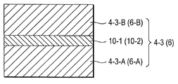
도 1에 도시된 자기저항효과소자는, 제1 전극(1); 5㎚의 두께를 갖는 Ta 층과 2㎚의 두께를 갖는 Ru 층으로 형성된 기판층(2), 15㎚ 정도의 두께를 가지며 PtMn 재료로 형성된 반강자성층(3); 3 내지 4 ㎚ 정도의 두께를 가지며 Co90Fe10 재료로 형성된 제1 자화 고착층(4-1)과, 약 0.9㎚의 두께를 가지며 Ru 재료로 형성되는 자화 반평행 결합층(4-2)과, 기능층(10-1)이 그 사이에 개재되면서 약 1.5㎚ 두께의 Co90Fe10 층에 본딩된 제2 자화 고착층(4-3)을 포함하는 자화 고착층(4); Cu 재료로 형성되고 3 ㎚ 정도의 두께를 갖는 스페이서층(5); 자화 자유층(6); 제1 보호층(7); 제2 보호층(8); 및 제2 전극(9)을 적층하여 형성되는 구조를 갖는다. The magnetoresistive element shown in FIG. 1 includes a
제1 자화 고착층(4-1)의 자화는 인접한 반강자성층(3)에 의해 본질적으로는 한 방향으로 고착된다. 제2 자화 고착층(4-3)의 자화는 자화 반평행 결합층(4-2)을 통해서 제1 자화 고착층에 반평행한 방향으로 고착된다. 자화 자유층(6)은 그 자화가 외부 자계에 따라서 변화할 수 있는 강자성층을 포함한다. 스페이서층(5)은 제2 자화 고착층(4-3)과 자화 자유층(6) 간의 자기적 결합을 차단하는 층이다. 도 1에 도시된 자기저항효과소자에서, 스페이서층(5)은 금속으로만 형성된다. The magnetization of the first magnetization fixing layer 4-1 is essentially fixed in one direction by the adjacent
상기 구성을 갖는 자기저항효과소자는 이하에서 언급하는 대로 제조된다. 먼저, 5㎚의 Ta 층과 2㎚의 Ru층이, 제1 전극(1)이 될, Cu, NiFe, Ta, Ru, CuAg 등과 같은 재료 위에, DC 마그네트론 스퍼터링에 의해서 적층되어 기판층(2)을 형성하게 된다. The magnetoresistive element having the above structure is manufactured as mentioned below. First, a Ta layer of 5 nm and a Ru layer of 2 nm are laminated by DC magnetron sputtering on a material such as Cu, NiFe, Ta, Ru, CuAg, etc., which will be the
반강자성층(3)이 될 PtMn이, 기판층(2)이 형성되었던 분위기를 깨뜨리지 않고, DC 마그네트론 스퍼터링에 의해서 기판층(2) 위에 15㎚의 두께로 형성된다. 반강자성층(3)의 형성 후에, Co90Fe10 이 반강자성층(3) 위에 3 내지 4㎚의 두께로 적층되어 제1 자화 고착층(4-1)을 형성하게 된다. Ru가 0.9㎚의 두께로 적층된 결과, 자화 반평행 결합층(4-2)이 형성된다. 다음 순서로, 적층 구성원인, 즉 제2 자화 고착층(4-3)인 Co90Fe10 이 1.5㎚의 두께로 적층된다. 제2 자화 고착층(4-3)을 형성하는 동안에, 기능층(10-1)이 도 2a 내지 도 2e에 도시된 프로세스에 의해서 제2 자화 고착층(4-3) 내에 형성된다. PtMn to be the
특정하게는, 상기 프로세스는 이하와 같다. 먼저, Fe가 피산화층이 될 제2 자화 고착층(4-3)의 일부로서 1㎚의 두께로 성장된다. 여기서, '제2 자화 고착층(4-3)의 일부' 라는 용어는 기능층(10)이 그 사이에 개재되어 상부 및 하부 영역으로 나뉘는 제2 자화 고착층의 하부 절반을 의미한다. Specifically, the process is as follows. First, Fe is grown to a thickness of 1 nm as a part of the second magnetized fixing layer 4-3 to be an oxide layer. Here, the term 'part of the second magnetization fixing layer 4-3' refers to the lower half of the second magnetization fixing layer divided into the upper and lower regions with the
제2 자화 고착층(4-3)의 일부인 Fe의 표면을 자연 산화, 이온빔 산화(IAO:Ion Assisted Oxidation), 또는 플라즈마 산화를 겪게 하여, 기능층(10-1)이 Fe의 표면 위에서 약 1.5㎚ 에서 3㎚의 두께로 성장하도록 야기한다. 여기서, IAO는 산소를 Ar 이온빔에 노출시키면서 산소를 챔버 내로 도입하여 산화를 일으키기 위한 프로세스이다. 상세 내용으로는, 이하의 관련 문헌 3을 참조하라. The surface of Fe which is part of the second magnetized adhesion layer 4-3 is subjected to spontaneous oxidation, ion assisted oxidation (IAO), or plasma oxidation, so that the functional layer 10-1 is about 1.5 above the surface of Fe. Causes growth to a thickness of 3 nm at nm. Here, IAO is a process for inducing oxygen by introducing oxygen into the chamber while exposing oxygen to an Ar ion beam. For details, see
관련 문헌 3: "J. Appl. Phys. 91,6684(2002)."Related Document 3: "J. Appl. Phys. 91,6684 (2002)."
이온빔은 통상의 밀링(milling) 요구 조건에 따라 채택되는 것보다 매우 약하고, 빔 전압은 100V 또는 그 이하로 설정된다. 이런 요구 조건 하에서 Fe를 산소 없이 이온빔에 노출하였을 때 획득되는 에칭 레이트는 0.1 내지 3 옹스트롬/분 정도의 값을 갖는다. The ion beam is much weaker than that adopted in accordance with conventional milling requirements, and the beam voltage is set at 100V or less. The etching rate obtained when Fe is exposed to an ion beam without oxygen under these requirements has a value on the order of 0.1 to 3 Angstroms / minute.
자연 산화, IAO, 및 플라즈마 산화에 관한 프로세스 요구 조건은 도 12에 도시된 표1에서 제공되었다. Process requirements for natural oxidation, IAO, and plasma oxidation are provided in Table 1 shown in FIG.
표1에서, 참조 부호 REF는, 참조될 샘플로서, 어떤 기능층도 갖지 않은 스핀 밸브 구조의 프로세스를 표시한다. 참조 부호 A-1 내지 A-4는 기능층을 준비하는 관련 프로세스에 대한 프로세스 조건을 표시한다. 참조 부호 B-1 내지 B-4는 본 발명의 기능층을 준비하는 프로세스에 대한 프로세스 조건들을 표시한다. In Table 1, reference numeral REF indicates the process of the spin valve structure without any functional layer, as a sample to be referenced. Reference numerals A-1 to A-4 denote process conditions for the relevant process for preparing the functional layer. Reference numerals B-1 to B-4 denote process conditions for the process of preparing the functional layer of the present invention.
기능층을 준비하는 종래의 프로세서에 관한 프로세스 조건과 기능층을 준비하는 본 발명의 프로세스에 관한 프로세스 조건 간의 차이는, AIT(After Ion Treatment), 즉 약한 이온빔의 조사가, 산화물 박막이 자연 산화, IAO, 및 플라즈마 산화 중의 임의의 것에 의해 형성될 때, 수행된다는 점에 있다. AIT는 매우 약 한 밀링에 의해 Fe50Co50-O 로부터 박막을 형성하기 위한 것이다. 이전에 기술된 IAO의 경우에서처럼, 매우 약한 이온 빔 조건이 본 경우에 요구된다. 예를 들어, AIT 가, 수십 나노미터 정도의 두께를 갖는 후막이 밀링에 의해 제거될 경우에 채택되는, 200V 또는 그 이상의 빔 전압과 100㎃ 또는 그 이상의 빔 전류라는 조건 하에서 수행될 때, 도 11에 도시된 대로 균일한 기능층(10)이 준비될 수 없다. 처리(treat)된 막 표면은 거칠거칠하게 되고, 이는 감지 전자 전류(17)가 기능층(10)을 통해서 부분적으로만 흐르게 되기 때문에 MR 비를 감소시키는 결과를 낳는다. 본 발명의 AIT 는 기능층이 섬 형상으로 형성되거나 또는 다수의 핀 홀이 기능층 내에 형성되는 결과를 낳지 않는다. 기능층(10)이 될 산화물 막은 도 3에 도시된 대로 균일한 두께를 갖는 박막이 되도록 형성될 수 있다. 그 결과, 전류(17)의 전체가 기능층(10)을 통해서 흐를 수 있어서 높은 MR비가 획득될 수 있다. The difference between the process conditions for the conventional processor for preparing the functional layer and the process conditions for the process of the present invention for preparing the functional layer is that AIT (After Ion Treatment), that is, irradiation of a weak ion beam, causes the oxide thin film to naturally oxidize, When formed by IAO, and any of plasma oxidation. AIT is for forming a thin film from Fe 50 Co 50 -O by very weak milling. As in the case of the previously described IAO, very weak ion beam conditions are required in this case. For example, when AIT is performed under the condition of a beam voltage of 200 V or more and a beam current of 100 mA or more, which is adopted when a thick film having a thickness of several tens of nanometers is removed by milling, FIG. The uniform
기능층(10)이 이상의 프로세스에 의해 형성된 후에, 제2 자화 고착층(4-3)의 상부 절반을 형성하게 되는 Co90Fe10 이 형성되어 제2 자화 고착층(4-3)을 완성시키게 된다. 다음으로, Cu 재료로 만들어진 스페이서층(5)이 제2 자화 고착층(4-3) 위에 3㎚의 두께로 형성된다. After the
스페이서층(5)의 형성 후에, 자화 자유층(6)이 형성된다 제2 자화 고착층(4-3)의 경우와 같이, 자화 자유층(6)은 기능층(10-2)를 포함할 수 있다. 이번에 채택되는 제조 프로세스도 제2 자화 고착층(4-3)을 제조하는 프로세스와 본질적으로 동일하기 때문에 그 설명은 생략된다. After formation of the
자화 자유층(6)의 형성 후에, Cu 재료로 형성된 제1 보호층과 Ru 재료로 형성된 제2 보호층(8)이, DC 바이어스를 이용한 마그네트론 스퍼터링에 의해서 진공 하에 계속 있으면서, 형성된다. After the formation of the magnetization
최종적으로, Cu, NiFe, Ta, Ru, CuAg 등과 같은 재료가 제2 보호층(8)의 표면 위에서 성장하도록 야기되어, 제2 전극(9)을 형성하게 된다. 이상 언급한 프로세스를 통해서, 자기저항효과소자가 완성된다. Finally, materials such as Cu, NiFe, Ta, Ru, CuAg and the like are caused to grow on the surface of the second
본 실시예에서, 기능층(10)은 Fe의 산화물로서 취해진다. 그러나, 기능층(10)은 이 재료에만 국한되지 않는다. 기능층(10)에 대한 본질적인 요구 조건은, Fe, Co, Ni, Cu, Ti, V, Cr, Mn, Mg, Al, Si, Zr, Nb, Mo, Ru, Rh, Pd, Ag, Hf, Ta, W, Re, Ir, Pt 및 Au로 구성된 그룹으로부터 선택된 적어도 하나의 성분을 함유하는 금속 또는 합금을 산화하거나, 질화시키거나, 불화(fluorinate)시켜서 형성된 산화물, 질화물, 또는 불화물이어야 한다는 점이다. In the present embodiment, the
본 발명의 제1 실시예에 따른 제조 방법으로 제조된 자기저항효과소자와 종래의 제조 방법으로 제조된 자기저항효과소자의 속성들 간의 차이가 표1을 참조하여 설명될 것이다.The difference between the properties of the magnetoresistive element manufactured by the manufacturing method according to the first embodiment of the present invention and the magnetoresistive effect element manufactured by the conventional manufacturing method will be described with reference to Table 1.
표1을 보면, 기능층(10)이 종래 기술 프로세스에 따라서 형성된 A-1, A-2, A-3 및 A-4에서, MR비는 기능층이 형성되지 않은 샘플 REF와 비교하여 증가된다. 그러나, 상당한 정도의 증가가 발견되지는 않았다. 대조적으로, 기능층이 본 발명의 프로세스에 따라 형성된 때의 샘플들인 B-1, B-2, B-3 및 B-4에서는, 본 발명의 프로세스를 따라 준비된 샘플들에 대응하여, MR비가 10 팩터(factor) 정도 증가된 다. 따라서, 본 발명의 샘플들의 유리한 점이 주목할만하다. 그 이유는 도 3에 도시된 것과 같은 균일한 기능층이, 샘플들 A-1, A-2, A-3 및 A-4 의 기능층들이 도 11에 도시된 섬 형상으로 형성되는 것과는 대조적으로, 샘플들 B-1, B-2, B-3 및 B-4 내에 형성되기 때문이다. Referring to Table 1, in A-1, A-2, A-3, and A-4 where the
도 6a는 본 발명의 프로세스를 통해서 준비된 기능층들(10-1, 10-2) 근방에서의 에어리어의 단면 TEM(Transmission electron microscope) 이미지이다. 도해된 샘플들에서, 기능층들(10-1, 10-2)은 산화물 층들이고, 따라서 주변 에어리어들의 것보다 더 백색의 콘트라스트가 획득된다. 백색 콘트라스트에 의해서, 기능층들이 균일한지 또는 조각난 섬 형상을 갖는지에 대한 판정이 이뤄질 수 있다. 도 6a에 도시된 대로, 샘플이 전자선 투과 방향으로 가능한 한 얇게 슬라이스(slice)된다 하더라도, 본질적으로 곧게 뻗은 기능층들(10-1, 10-2)은 어떤 비연속성도 없고, 매우 얇다. 한편, 도 6b는 종래 기술의 프로세스를 통해서 준비된 기능층들(10-1, 10-2)의 에어리어의 단면 TEM 이미지이다. 도 6a와는 대조적으로, 기능층들(10-1, 10-2)은 비연속성을 갖는 것으로 단정할 수 있다. 6A is a cross-sectional transmission electron microscope (TEM) image of the area in the vicinity of functional layers 10-1 and 10-2 prepared through the process of the present invention. In the illustrated samples, the functional layers 10-1 and 10-2 are oxide layers, so that a whiter contrast than that of the surrounding areas is obtained. By white contrast, a determination can be made as to whether the functional layers have a uniform or fragmented island shape. As shown in FIG. 6A, even if the sample is sliced as thin as possible in the electron beam transmission direction, the essentially straight functional layers 10-1 and 10-2 have no discontinuity and are very thin. 6B is a cross-sectional TEM image of an area of functional layers 10-1 and 10-2 prepared through a prior art process. In contrast to FIG. 6A, the functional layers 10-1 and 10-2 may be assumed to have discontinuities.
도 6a 및 도 6b에서, 기능층들(10-1, 10-2)은 백색을 띠고 그외의 부분들로부터 뚜렷하게 구별될 수 있다. 기능층들을 구별하기 힘들 때는, 그 크기가 1 ㎚ 정도로 좁혀진 빔을 채택한 EDX(Energy Dispersive X-ray Spectrosopy)에 의해서 기능층들이 식별될 수 있다. 이 경우에, 막의 성장 방향을 따라 0.5 ㎚ 내지 1㎚의 간격으로 측정 포인트들이 제공된다. 기능층들은 측정 포인트들에 대해서 소자의 분포가 그려졌을 때 획득되는, 산소, 질화물, 인광물질(phosphor), 플루오르 등 과 같은 것의 농도 분포의 반값 폭(half-value width)으로부터 계산될 수도 있다. In FIGS. 6A and 6B, the functional layers 10-1 and 10-2 are white in color and can be clearly distinguished from the other parts. When the functional layers are difficult to distinguish, the functional layers can be identified by Energy Dispersive X-ray Spectrosopy (EDX) employing a beam whose size is narrowed down to 1 nm. In this case, measurement points are provided at intervals of 0.5 nm to 1 nm along the growth direction of the film. The functional layers may be calculated from the half-value width of the concentration distribution of such as oxygen, nitride, phosphor, fluorine, etc., obtained when the device distribution is plotted relative to the measurement points.
도 7은 AIT 에 대한 조건이 샘플 B-2에 대해서 변화했을 때에 획득되는 결과를 보여주는데, 이는 본 발명의 전형적 예의 프로세스이다. 프로세싱 시간은 막이 Fe50Co50-O 재료로부터 0.3 ㎚ 의 두께로 형성되도록 조정되고 변화된다. 그 결과로부터 알 수 있는 것처럼, 빈 전압이 110V 를 초과하면 MR 비는 감소한다. 빔 전압이 210V까지 증가될 때, MR 비는 0.3%의 값을 가진다고 이해되는데, 이는 어떤 기능층도 없는 샘플 REF의 경우에 획득된 MR 비보다 낮은 것이다. 이 실험 결과로부터, AIT의 빔 전압은 양호하게는 110V 또는 그 이하가 된다. 7 shows the results obtained when the conditions for AIT changed for Sample B-2, which is a typical example process of the present invention. The processing time is adjusted and varied so that the film is formed to a thickness of 0.3 nm from the Fe 50 Co 50 -O material. As can be seen from the result, the MR ratio decreases when the empty voltage exceeds 110V. When the beam voltage is increased to 210V, it is understood that the MR ratio has a value of 0.3%, which is lower than the MR ratio obtained for the sample REF without any functional layer. From this experimental result, the beam voltage of the AIT is preferably 110V or less.
RF 플라즈마의 조사는 또는 매우 약한 에너지 조건들을 요구한다. 이 에너지의 적합한 범위는 15W 내지 30W이다. 대조적으로, 기판을 세정하기 위해 사용되는 100W 등의 강한 에너지 조건 하에서는, 막의 표면은 열화되어 MR 비가 감소된다. Irradiation of the RF plasma or requires very weak energy conditions. A suitable range of this energy is 15W to 30W. In contrast, under strong energy conditions, such as 100 W, used to clean the substrate, the surface of the film is degraded to reduce the MR ratio.
(제1 변형예)(First modification)
도 4는 도 1에 도시된 제1 실시예의 제1 변형예로서, 삼층 구조(복합 구조, synthetic structure)가 아닌 단일 자화 고착층을 갖는 자기저항효과소자를 도시하였다. FIG. 4 is a first modification of the first embodiment shown in FIG. 1, and illustrates a magnetoresistive element having a single magnetized fixing layer rather than a three-layer structure (synthetic structure).
도 4에서 본 변형예의 자기저항효과소자는, 제1 전극(1'), 5㎚의 두께를 갖는 Ta층/2㎚의 두께를 갖는 Ru층을 포함하는 기판층(2'), 15㎚ 정도의 두께로 PtMn 재료로 형성되는 반강자성층(3'), Co90Fe10 층으로부터 형성된 자화 고착층(4'), 3㎚ 정도의 두께로 Cu로 형성된 스페이서층(5'), Co90Fe10 층으로 형성된 자화 자유층(6'), 약 1㎚의 두께로 Cu로 형성된 제1 보호층(7'), 약 5㎚의 두께로 Ru로부터 형성된 제2 보호층(8'), 및 제2 전극(9')이 적층된 구조를 갖는다. 기능층(10')은 자화 고착층(4') 내로 삽입된다. As shown in Fig. 4, the magnetoresistive element of the modified example includes a first electrode 1 ', a substrate layer 2' including a Ta layer having a thickness of 5 nm and a Ru layer having a thickness of 2 nm, about 15 nm. An antiferromagnetic layer 3 'formed of a PtMn material at a thickness of 3', a magnetized fixing layer 4 'formed from a Co 90 Fe 10 layer, a spacer layer 5' made of Cu at a thickness of about 3 nm, and a Co 90 Fe Magnetization free layer 6 'formed of ten layers, a first protective layer 7' formed of Cu to a thickness of about 1 nm, a second protective layer 8 'formed from Ru to a thickness of about 5 nm, and It has a structure in which two electrodes 9 'are stacked. The functional layer 10 'is inserted into the magnetization fixing layer 4'.
제1 변형예에서도, 제1 실시예에서 획득된 효과와 유사한 효과가 산출된다. Also in the first modification, an effect similar to the effect obtained in the first embodiment is calculated.
(제2 변형예)(Second modification)
도 5는 도 1에 도시되는 제1 실시예의 제2 변형예로서, 스페이서층을 개재하여, 자화 고착층 및 자화 자유층의 위치가, 도 1에 도시된 제1 실시예의 자화 고착층 및 자화 자유층의 위치와 역으로 되어 있는 자기저항효과소자를 도시한다.FIG. 5 is a second modification of the first embodiment shown in FIG. 1, wherein the positions of the magnetization fixing layer and the magnetization free layer are positioned via the spacer layer, and the magnetization fixing layer and the magnetization free of the first embodiment shown in FIG. 1. The magnetoresistive effect element is shown in reverse with the position of the layer.
도 5에 도시된 바와 같이, 본 변형예의 자기저항효과소자는, 제1 전극(1"); 5nm 두께의 Ta층 및 2nm 두께의 Ru층으로 형성된 기판층(2"); 기능층(10-2")을 협지하도록 1.5nm 정도의 Co90Fe10층을 자화층에 부착(affix)함으로써 형성된 자화 자유층(6"); Cu로 형성되고 막 두께가 3nm 정도인 스페이서층(5"); 기능층(10-1")을 협지하도록 1.5nm 정도의 Co90Fe10층을 자화층에 부착함으로써 형성된 제2 자화 고착층(4-3"); Ru로 형성되고 막 두께가 0.9nm 정도인 자화 반평행 결합층(4-2"); Co90Fe10으로 형성되고 막 두께가 3~4nm 정도인 제1 자화 고착층(4-1"); PtMn으로 형성되고 막 두께가 15nm 정도인 반강자성층(3"), Ru로 형성되고 막 두께가 5nm 정도인 보호층(8"), 및 제2 전극(9")을 적층한 구조를 갖는다. 제2 변형예에서도, 제1실시예와 마찬가지의 효과가 얻어진다.As shown in Fig. 5, the magnetoresistive element of this modification includes a
(제2 실시예)(2nd Example)
지금부터, 본 발명의 제2 실시예의 자기저항효과소자의 제조 방법을 설명한다. 제2 실시예는 기능층의 재료가 변경된다는 점에서 제1 실시예와는 다르다. 따라서, 제1 실시예와 제2 실시예간의 명확한 차이점에 대하여 설명하고, 유사한 부분에 대해서는 생략한다.The manufacturing method of the magnetoresistive element of the second embodiment of the present invention will now be described. The second embodiment differs from the first embodiment in that the material of the functional layer is changed. Therefore, clear differences between the first embodiment and the second embodiment will be described, and similar parts will be omitted.
제1 전극(1)에서 자화 반평행 결합층(4-2)까지를 제1 실시예에서 설명하는 프로세스들을 통해 형성한 후에, 적층 부재이며 제2 자화 고착층(4-3)으로서 역할을 하는 Co90Fe10을 1.5nm로 적층한다. 제2 자화 고착층(4-3)의 형성 과정 중에, 도 2의 (a) 내지 도 2의 (e)에 도시된 바와 같은 프로세스를 통해 기능층(10-1)을 형성한다.After forming from the
구체적으로는, 프로세스들은 다음과 같다. 먼저, 피산화층으로 되는 제2 자화 고착층(4-3)의 일부로서 Fe50Co50을 1nm 두께로 성장시킨다. 여기서, "제2 자화 고착층(4-3")의 일부"란, 제1 실시예에서도 설명한 바와 같이, 기능층(10-1)을 협지하여 상하로 분단된 제2 자화 고착층의 아래 절반을 의미한다.Specifically, the processes are as follows. First, Fe 50 Co 50 is grown to a thickness of 1 nm as part of the second magnetized fixing layer 4-3 to be the layer to be oxidized. Here, "part of the second magnetization adhesion layer 4-3" is the lower half of the second magnetization adhesion layer divided up and down by sandwiching the functional layer 10-1 as described in the first embodiment. Means.
재2 자화 고착층(4-3)의 일부인 Fe50Co50의 표면은 자연 산화, 이온 빔 산화(IAO : Ion Assisted Oxidation), 또는 플라즈마 산화 처리되어, Fe50Co50의 표면에 약 1.5nm 내지 3nm 두께의 기능층(10-1)이 성장하게 된다. 여기서, 이온 빔은 통상의 밀링 조건에서 비해서 매우 약해, 빔 전압은 100V 이하로 설정하고 있다. 이 조건에서의 이온 빔을 산소 없이 하여 Co90Fe10에 조사한 경우의 에칭 레이트는 3Å/min 정도이다.The surface of Fe 50 Co 50 , which is part of the second magnetization fixing layer 4-3, is subjected to spontaneous oxidation, ion beam oxidation (IAO), or plasma oxidation, so that the surface of Fe 50 Co 50 is about 1.5 nm to The 3 nm thick functional layer 10-1 is grown. Here, the ion beam is very weak compared with normal milling conditions, and the beam voltage is set at 100 V or less. The etching rate in the case of irradiating Co 90 Fe 10 with the ion beam under these conditions without oxygen is about 3 μs / min.
자연 산화, IAO 및 플라즈마 산화에 대한 프로세스 조건은 도 13에 도시된 표 2에 제공된 바와 같다.Process conditions for natural oxidation, IAO and plasma oxidation are as provided in Table 2 shown in FIG.
표 2에서,참조 기호 REF는 참조용 샘플로서 기능층이 없는 스핀 밸브 구조의 프로세스를 나타내고 있다. C-1∼C-4는, 종래의 기능층 작성 프로세스의 프로세스 조건을 나타내고 있다. D-1∼D-4는 본 발명의 기능층 작성 프로세스의 프로세스 조건을 나타내고 있다.In Table 2, the reference symbol REF shows the process of the spin valve structure without a functional layer as a reference sample. C-1 to C-4 have shown the process conditions of the conventional functional layer creation process. D-1 to D-4 represent the process conditions of the functional layer creation process of the present invention.
종래의 기능층 작성 프로세스의 프로세스 조건과의 차이는, 제1 실시예에서와 같이, 자연 산화, IAO 및 플라즈마 산화 중 어느 하나로 형성된 산화막을 박막화 할 때에 AIT(After Ion Treatment)를 행하고 있는 것이다. 이 AIT를 행함으로써, 기능층(10)을, 섬 형상이 되거나, 복수의 핀 홀을 갖지 않고, 일정한 두께를 유지하면서 박막층으로 형성될 수 있다.The difference from the process conditions of the conventional functional layer creation process is that after Ion treatment (AIT) is performed when the oxide film formed by any one of natural oxidation, IAO and plasma oxidation is thinned as in the first embodiment. By performing this AIT, the
기능층(10)을 전술한 프로세스에 의해 형성 한 후, 제2 자화 고착층(4-3)의 위의 절반이 되는 Co90Fe10을 형성하는 프로세스로부터 제2 전극(9)을 형성할 때까지의 프로세스는 제1 실시예와 마찬가지이기 때문에,설명을 생략한다.When the
또한, 본 실시예에서는, 기능층(10)을 FeCo의 산화물이라고 하고 있지만, 제1 실시예와 마찬가지로, 이것에 한정되지 않는다. Fe, Co, Ni, Cu, Ti, V, Cr, Mn, Mg, Al, Si, Zr, Nb, Mo, Ru, Rh, Pd, Ag, Hf, Ta, W, Re, Ir, Pt, Au로 이루 어진 그룹으로부터 선택된 적어도 하나의 부재를 포함하는 금속 혹은 합금을 산화, 질화, 플루오르화함으로써 얻을 수 있는 산화물, 질화물, 또는 플루오르화물이면 된다.In addition, in this embodiment, although the
다음에 본 발명의 제2 실시예의 제조 방법으로 제작한 자기저항효과소자와 종래의 제조 방법으로 제작한 자기저항효과소자와의 특성상의 차이에 대해서 표 2를 이용하여 설명한다. 표 2로부터, 기능층(10)의 모재로서 FeCo 합금을 이용했을 경우에도, 종래의 프로세스 플로우로 작성한 샘플 그룹 C에서는 MR 증가량이 크지는 않았다. 그러나, 본 발명의 프로세스 플로우로 작성한 샘플 그룹 D에서의 MR 증가량은 매우 크다. 이것도, 똑같은 기능층(10)이 그룹 D에서 얻어지기 때문에라고 생각된다.Next, the difference in characteristics between the magnetoresistive element produced by the manufacturing method of the second embodiment of the present invention and the magnetoresistive element manufactured by the conventional manufacturing method will be described using Table 2. From Table 2, even when FeCo alloy was used as the base material of the
제2 실시예의 방법에서 자기저항효과소자를 형성한 경우, 조건을 제1 실시예와 동일하게 빔 전압 100V이하, RF 플라즈마로 한 경우에는 RF 파워를 l5W로부터 30W로 한 경우에만, 기능층의 효과를 충분히 활용할 수 있고, 높은 MR를 얻을 수 있다.In the case of forming the magnetoresistive element in the method of the second embodiment, the effect of the functional layer only when the RF power is set from l5W to 30W when the condition is set to a beam voltage of 100V or less and RF plasma as in the first embodiment. Can be utilized sufficiently and a high MR can be obtained.
또한, 제1 실시예와 제2 실시예의 조성을 포함하는 Co1 - XFex 합금(50≤x≤1O0)을 이용하면, 더욱 고 MR화를 실현할 수 있다.Further, by using the Co 1 - X Fex alloy (50≤x≤100) including the compositions of the first embodiment and the second embodiment, higher MR can be realized.
(제3 실시예) (Third Embodiment)
다음에 본 발명의 제3 실시예인 자기저항효과소자의 제조 방법에 대해서 설명한다. 제3 실시예에서는, 제2 실시예와 같이 제1 실시예의 기능층(10)과는 그 재 료를 변화시키고 있는 점에 있다. 따라서, 제1 실시예와 명확하게 다른 부분에 대해서 설명하고, 같은 부분에 대해서는 설명을 생략한다.Next, a method of manufacturing a magnetoresistive element as a third embodiment of the present invention will be described. In the third embodiment, the material is changed from the
제1 전극(1)으로부터 자화 반평행 결합층(4-2)까지를 제1 실시예에 기재된 프로세스로 형성한 후, 적층 부재이고 제2 자화 고착층(4-3)인 Co90Fe10을 1.5nm로 적층한다. 이 제2 자화 고착층(4-3)의 형성 과정 중에, 도 2의 (a) 내지 (e)에 도시한 바와 같은 프로세스에 의해 기능층(10-1)을 형성한다.After forming from the
구체적으로는,다음과 같은 프로세스다. 우선,피산화층이 되는 제2 자화 고착층(4-3)의 일부로서 Ti를 1nm의 두께로 성장시킨다. 여기서 "제2 자화 고착층(4-3)의 일부"란, 제1 실시예에서도 설명한 바와 같이, 기능층(10-1)을 협지하여 상하로 분단된 제2자화 고착층의 아래 절반을 의미한다.Specifically, the process is as follows. First, Ti is grown to a thickness of 1 nm as a part of the second magnetized fixing layer 4-3 to be an oxidation layer. Here, "part of the second magnetization fixing layer 4-3" refers to the lower half of the second magnetization fixing layer divided up and down by sandwiching the functional layer 10-1 as described in the first embodiment. do.
다음으로,상기 제2 자화 고착층(4-3)의 일부인 Ti의 표면을 자연 산화, 혹은 이온 빔 산화(IAO : lon Assisted 0xidation), 혹은 플라즈마 산화함으로써, 이 표면에 막 두께 1.5∼3nm 정도의 기능층(10-1)을 성장시킨다. 이온 빔은 통상의 밀링 조건에 비교해서 매우 약하게, 빔 전압을 I0OV 이하로 설정하고 있다. 이 조건에서의 이온 빔을 산소가 없이 하여 Ti에 조사했을 경우의 에칭 레이트는, 0.1∼3Å/min 정도다.Next, the surface of Ti, which is a part of the second magnetized fixing layer 4-3, is naturally oxidized, ion beam oxidation (IAO: lon Assisted 0xidation), or plasma oxidation, and the surface has a thickness of about 1.5 to 3 nm. The functional layer 10-1 is grown. The ion beam sets the beam voltage to I0OV or less very weakly compared to normal milling conditions. The etching rate in the case of irradiating Ti with an ion beam under this condition without oxygen is about 0.1 to 3 mW / min.
자연 산화, IAO 및 플라즈마 산화 각각의 프로세스 조건은 표 3에 도시한다.The process conditions for natural oxidation, IAO and plasma oxidation, respectively, are shown in Table 3.
표 3에서,참조 번호 REF는 참조용 샘플로서 기능층이 없은 스핀 밸브 구조의 프로세스를 나타내고 있다. E-1∼E-4는, 종래의 기능층 작성 프로세스의 프로 세스 조건을 나타내고 있다. F-1∼F-4는 본 발명의 기능층 작성 프로세스의 프로세스 조건을 나타내고 있다.In Table 3, reference numeral REF indicates a process of a spin valve structure without a functional layer as a reference sample. E-1 to E-4 show the process conditions of the conventional functional layer creation process. F-1 to F-4 have shown the process conditions of the functional layer preparation process of this invention.
종래의 기능층 작성 프로세스의 프로세스 조건과의 차이는, 제1 실시예와 같이 자연 산화, IAO 및 플라즈마 산화 중 어느 하나에 의해 형성된 산화막을 박막화 할 때에 AIT(After Ion Treatment)를 행하고 있는 것이다. 이 AIT를 행함으로써, 기능층(10)을, 섬 형상이 되거나, 복수의 핀 홀을 갖지 않고, 균일한 막 두께를 유지하면서 박막화하는 것이 가능하게 된다.The difference from the process conditions of the conventional functional layer creation process is that AIT (After Ion Treatment) is performed when the oxide film formed by any one of natural oxidation, IAO and plasma oxidation is thinned as in the first embodiment. By performing this AIT, the
기능층(10)을 전술한 프로세스에 의해 형성 한 후, 제2 자화 고착층(4-3)의 위의 절반이 되는 Co90Fe10을 형성하는 프로세스로부터 제2 전극(9)을 형성할 때 까지의 프로세스는 제1 실시예와 마찬가지이기 때문에,설명을 생략한다.When the
또한,본 실시예 에서는,기능층(10)을 Ti의 산화물이라고 하고 있다. 그러나, 이것에 한정되지 않고, Fe, Co, Ni, Cu, Ti, V, Cr, Mn, Mg, Al, Si, Zr, Nb, Mo, Ru, Rh, Pd, Ag, Hf, Ta, W, Re, Ir, Pt 및 Au로 이루어지는 그룹으로부터 선택된 적어도 하나의 금속 혹은 합금을 산화, 질화, 플루오르화함으로써 얻을 수 있는 산화물, 질화물,또는 플루오르화물이면 된다.In this embodiment, the
본 발명의 제3 실시예의 제조 방법으로 제작한 자기저항효과소자와 종래의 제조 방법으로 제작한 자기저항효과소자와의 특성상의 차이에 대해서 표 3을 이용하여 설명한다. 기능층의 모재로서 Ti를 이용했을 경우에도, 종래의 프로세스 플로우로 작성한 샘플 그룹 E에서는 MR증가량이 크지는 않았다. 그러나, 본 발명의 프로세스 플로우로 작성한 샘플 그룹 F에서의 MR 증가량은 매우 크다. 이것도, 똑같은 기능층이 그룹 F에서 얻어지기 때문에라고 생각된다.The difference in characteristics between the magnetoresistive element produced by the manufacturing method of the third embodiment of the present invention and the magnetoresistive effect element produced by the conventional manufacturing method will be described using Table 3. Even when Ti was used as the base material of the functional layer, the amount of MR increase was not large in sample group E prepared by the conventional process flow. However, the MR increase amount in the sample group F created by the process flow of the present invention is very large. This is also considered to be because the same functional layer is obtained from the group F.
제3 실시예의 방법에서 자기저항효과소자를 형성했을 경우, 조건을 제1 실시예와 동일하게 빔 전압 100V이하, RF 플라즈마라고 했을 경우에는, RF 파워를 l5W로부터 30V로 했을 경우에만, 기능층의 효과를 충분히 활용할 수 있고, 높은 MR을 얻을 수 있다. When the magnetoresistive element is formed in the method of the third embodiment, the conditions are the same as in the first embodiment, the beam voltage is 100V or less, and the RF plasma is used. The effect can be fully utilized, and a high MR can be obtained.
(제4 실시예)(Example 4)
다음으로, 본 발명의 제4 실시예의 자기저항효과소자의 제조 방법에 대해서 설명한다. 제4 실시예에서는,제2 실시예와 마찬가지로, 제1 실시예의 기능층(10)과는 그 재료를 변화시키고 있는 점에 차이가 있다. 따라서, 제1 실시예와 명확하게 차이가 되는 부분에 대해서 설명하고, 마찬가지의 부분에 대해서는 설명을 생략한다.Next, a method of manufacturing the magnetoresistive element of the fourth embodiment of the present invention will be described. In the fourth embodiment, similar to the second embodiment, there is a difference in that the material is changed from the
제1 전극(1)으로부터 자화 반평행 결합층(4-2)까지를 제1 실시예에 기재된 프로세스로 형성한 후, 적층 부재이고 제2 자화 고착층(4-3)인 Co90Fe10를 1.5nm적층한다. 이 제2 자화 고착증(4-3) 형성 과정 중에, 도 2의 (a) 내지 (e)에 도시한 바와 같은 프로세스에 의해 기능층(10-1)을 형성한다.After forming from the
구체적으로는,다음과 같은 프로세스다. 우선,피산화층이 되는 제2 자화 고착층(4-3)의 일부로서 Ti를 1nm의 두께로 성장시킨다. 여기서, "제2 자화 고착층(4-3)의 일부"란, 제1 실시예에서도 설명한 바와 같이, 기능층(10-1)을 협지하여 상하로 분단된 제2 자화 고착층의 아래 절반이다.Specifically, the process is as follows. First, Ti is grown to a thickness of 1 nm as a part of the second magnetized fixing layer 4-3 to be an oxidation layer. Here, "part of the second magnetization fixing layer 4-3" is the lower half of the second magnetization fixing layer which is divided up and down by sandwiching the functional layer 10-1 as described in the first embodiment. .
상기 제2 자화 고착층(4-3)의 일부인 Zr의 표면을 자연 산화, 이온 빔 산화(IAO), 혹은 플라즈마 산화함으로써, Zr의 표면에 막 두께 1.5 ~ 3nm 정도의 기능층(10-1)을 성막한다. 여기서, 이온 빔은 통상의 밀링 조건에 비해 매우 약하고, 빔 전압은 10OV 이하로 설정된다. 이 조건에서 이온 빔을 산소없는 Ti에 노출했을 경우의 에칭 레이트는 0.1 ~ 3Å/min(angstrom/min) 정도이다.The functional layer 10-1 having a thickness of about 1.5 to 3 nm on the surface of Zr by natural oxidation, ion beam oxidation (IAO), or plasma oxidation of the surface of Zr which is a part of the second magnetized fixing layer 4-3. Tabernacle Here, the ion beam is very weak compared to normal milling conditions, and the beam voltage is set to 10 OV or less. Under these conditions, the etching rate when the ion beam is exposed to oxygen-free Ti is about 0.1 to 3 dB / min (angstrom / min).
자연 산화, IAO, 및 플라즈마 산화 각각의 프로세스 조건은 도 15에 도시된 표 4에 주어진 바와 같다.Process conditions for natural oxidation, IAO, and plasma oxidation, respectively, are as given in Table 4 shown in FIG. 15.
표 4에서, 참조 부호 REF는, 참조용 샘플로서, 기능층이 없은 스핀 밸브 구조의 프로세스를 나타내고 있다. 참조 부호 G-1 ~ G-4는, 종래의 기능층 작성 프로세스의 프로세스 조건을 나타내고 있다. 참조 부호 H-1 ~ H-4는 본 발명의 기능층 작성 프로세스의 프로세스 조건을 나타내고 있다.In Table 4, reference numeral REF indicates a process of a spin valve structure without a functional layer as a reference sample. Reference numerals G-1 to G-4 indicate the process conditions of the conventional functional layer creation process. Reference numerals H-1 to H-4 indicate the process conditions of the functional layer creation process of the present invention.
종래의 기능층 작성 프로세스의 프로세스 조건과 본 발명의 기능층 작성 프로세스의 프로세스 조건 간의 차이는, 제1 실시예와 같이, 자연 산화, IAO, 및 플라즈마 산화 중 어느 하나에 의해 형성된 산화막을 박막화할 때 AIT(After Ion Treatment)를 행한다는 것이다. AIT를 행함으로써, 기능층(10)이, 섬 형상으로 형성되거나 복수의 핀홀을 갖지 않고 균일한 두께를 유지한 채 박막으로 형성되는 것이 가능하게 된다.The difference between the process conditions of the conventional functional layer creation process and the process conditions of the functional layer creation process of the present invention is similar to that of the first embodiment when thinning the oxide film formed by any one of natural oxidation, IAO, and plasma oxidation. It is to perform After Ion Treatment (AIT). By performing AIT, the
전술한 프로세스에 의해 기능층(10)을 형성 한 후, 제2 자화 고착층(4-3)의 상측 반쪽(upper half)이 되는 Co90Fe10를 형성하는 프로세스로부터 제2 전극(9)을 형성하는 프로세스까지의 프로세스들은 제1 실시예와 마찬가지이므로, 여기서 그에 대한 설명은 생략한다.After forming the
본 실시예에서는, 기능층(10)을 Zr의 산화물로 한다. 그러나, 기능층(10)은 이 재료에 한정되지 않는다. 기능층(10)을 위한 필수 조건은 Fe, Co, Ni, Cu, Ti, V, Cr, Mn, Mg, Al, Si, Zr, Nb, Mo, Ru, Rh, Pd, Ag, Hf, Ta, W, Re, Ir, Pt 및 Au 중 적어도 하나를 포함하는 금속 혹은 합금을 산화, 질화, 또는 불화함으로써 형성된 산화물, 질화물, 또는 불화물이라는 것이다.In this embodiment, the
다음에, 본 발명의 제4 실시예의 제조 방법으로 제작한 자기저항 효과소자와 종래의 제조 방법으로 제작한 자기저항 효과소자와의 특성상의 차이에 대해 표 4를 참조하여 설명할 것이다. 기능층의 모재로서 Zr를 이용하는 경우에도, 종래의 프로세스 플로우에 따라 작성한 샘플 그룹 G에서는 MR 증가량이 크지 않다. 그러나, 본 발명의 프로세스 플로우로 작성한 샘플 그룹 H에서의 MR 증가량은 매우 크다. 이것도, 똑같은 기능층을 그룹 H에서 얻을 수 있기 때문인 것으로 생각된다.Next, the difference in characteristics between the magnetoresistive element manufactured by the manufacturing method of the fourth embodiment of the present invention and the magnetoresistive effect element produced by the conventional manufacturing method will be described with reference to Table 4. Even when Zr is used as the base material of the functional layer, the MR increase amount is not large in the sample group G prepared according to the conventional process flow. However, the MR increase amount in the sample group H created by the process flow of the present invention is very large. This is considered to be because the same functional layer can be obtained from the group H.
제4 실시예의 방법에서 자기저항 효과소자를 형성하는 경우, 제1 실시예와 동일한 조건 하에, 즉, 빔 전압 100V 이하인 RF 플라즈마로 한 경우에는, RF 파워를 15W ~ 30W로 설정하는 경우에만 기능층의 효과를 십분 활용할 수 있고, 높은 MR 비를 얻을 수 있다.In the case of forming the magnetoresistive element in the method of the fourth embodiment, the functional layer is set only when the RF power is set to 15 W to 30 W under the same conditions as in the first embodiment, that is, when the RF plasma has a beam voltage of 100 V or less. You can take full advantage of the effect of and obtain a high MR ratio.
제1 내지 제4 실시예에서는, 여러 가지 재료의 기능층(10)을 제조하는 방법 으로 도 2a ~ 2e에 도시한 박막화 공정이 유용한 것으로 나타냈다. 추가로, 기능층(10)으로 Ti, Cr, Zr, Hf, V, A1, Mg, 또는 Cu를 이용하는 경우에도, 동일한 방식으로 그 재료에 박막화 공정을 실시함으로써 똑같은 기능층을 얻을 수 있고, 높은 MR 비를 얻을 수 있다는 것이 이해될 것이다.In the first to fourth embodiments, the thinning process shown in Figs. 2A to 2E has been shown to be useful as a method for producing the
(제5 실시예)(Example 5)
이제, 본 발명의 제5 실시예에 따른 자기저항 효과소자의 제조 방법에 대해서 설명할 것이다. 제5 실시예는 제1 내지 제4 실시예와는 달리, 기능층(10)가 적층체로 되어 있다. 그 외에 대해서는 제5 실시예가 제1 내지 제4 실시예와 본질적으로 동일하기 때문에, 제5 실시예와 제1 내지 제4 실시예간의 명백히 다른 부분에 대해서 설명하고, 같은 부분에 대해서는 설명을 생략한다.Now, a method of manufacturing the magnetoresistive element according to the fifth embodiment of the present invention will be described. In the fifth embodiment, unlike the first to fourth embodiments, the
제1 전극(1)부터 자화 반평행 결합층(4-2)까지를 제1 실시예에 기재된 프로세스에 의해 형성한 후, 적층체이고 제2 자화 고착층(4-3)인 Co90Fe10를 1.5nm로 적층한다. 제2 자화 고착층(4-3)을 형성하는 과정 동안, 도 2a-2e에 도시한 바와 같은 프로세스에 의해 기능층(10-1)을 형성한다.A first electrode (1) from the magnetization anti-parallel coupling layer, the layered product after the one formed by the process described in the first embodiment to (4-2) and the second magnetically fixed layer (4-3) of Co 90 Fe 10 Is laminated at 1.5 nm. During the process of forming the second magnetized fixing layer 4-3, the functional layer 10-1 is formed by a process as shown in FIGS. 2A-2E.
구체적으로, 상기 프로세스들은 다음과 같다. 우선, 피산화층이 되는 제2 자화 고착층(4-3)의 일부로서 Fe를 0.15nm의 두께로 성막하고, 계속해서 Zr를 0.15nm의 두께로 성막한다. 여기서, "제2 자화 고착층(4-3)의 일부"라는 용어는, 제1 실시예에 있어서도 설명한 바와 같이, 기능층(10-1)을 개재하여 상부와 하부로 분단된 제2 자화 고착층 하측 반쪽(lower half)이다.Specifically, the processes are as follows. First, Fe is formed into a thickness of 0.15 nm as a part of the second magnetized fixing layer 4-3 to be an oxidation layer, and then Zr is formed into a thickness of 0.15 nm. Here, the term " part of the second magnetization fixing layer 4-3 ", as described in the first embodiment, is the second magnetization fixing part divided into the upper part and the lower part through the functional layer 10-1. Lower half of layer.
상기 제2 자화 고착층(4-3)의 일부인 Fe 및 Zr를 자연 산화, 이온 빔 산화(IAO), 혹은 플라즈마 산화함으로써, Fe 및 Zr의 표면에 막 두께 1.5 ~ 3nm 정도의 기능층(10-1)을 성막한다. 여기서, 이온 빔은 통상의 밀링 조건에 비해 매우 약하고, 빔 전압은 10OV 이하로 설정된다. 이 조건에서의 이온 빔을 산소 없이 Fe 및 Zr로 이루어진 다층체(multilayer body)에 조사했을 경우의 에칭 레이트는 약 0.1 ~ 3Å/min 정도이다.The functional layer 10-having a thickness of about 1.5 to 3 nm is formed on the surface of Fe and Zr by natural oxidation, ion beam oxidation (IAO), or plasma oxidation of Fe and Zr, which are part of the second magnetized fixing layer 4-3. We form 1). Here, the ion beam is very weak compared to normal milling conditions, and the beam voltage is set to 10 OV or less. The etching rate when the ion beam is irradiated to a multilayer body made of Fe and Zr without oxygen is about 0.1 to 3
자연 산화, IAO, 및 플라즈마 산화 각각의 프로세스 조건은 도 16에 도시된 표 5에 제공되는 바와 같다.Process conditions for natural oxidation, IAO, and plasma oxidation, respectively, are as provided in Table 5 shown in FIG.
표 5에서, 참조 부호 REF는, 참조용 샘플로서, 기능층이 없는 스핀 밸브 구조의 프로세스를 나타내고 있다. 참조 부호 I-1 ~ I-4는 종래의 기능층 작성 프로세스의 프로세스 조건을 나타내고 있다. 참조 부호 J-1 ~ J-4는 본 발명의 기능층 작성 프로세스의 프로세스 조건을 나타내고 있다.In Table 5, reference numeral REF denotes a process of a spin valve structure without a functional layer as a reference sample. Reference numerals I-1 to I-4 indicate the process conditions of the conventional functional layer creation process. Reference numerals J-1 to J-4 indicate the process conditions of the functional layer creation process of the present invention.
종래의 기능층 작성 프로세스의 프로세스 조건과 본 발명의 기능층 작성 프로세스의 프로세스 조건 간의 차이는, 제1 실시예의 경우와 마찬가지로, 자연 산화, IAO, 플라즈마 산화 중 어느 하나에 의해 형성된 산화막을 박막화할 때에 AIT(After Ion Treatment)를 행한다는 것이다. AIT를 행함으로써, 기능층(10)이, 섬 형상으로 형성되거나 복수의 핀홀을 갖지 않고 균일한 막 두께를 유지한채 박막화되는 것이 가능하다.The difference between the process conditions of the conventional functional layer creation process and the process conditions of the functional layer creation process of the present invention is similar to that of the first embodiment, when thinning the oxide film formed by any one of natural oxidation, IAO, and plasma oxidation. It is to perform After Ion Treatment (AIT). By performing AIT, the
기능층(l0)을 전술한 프로세스에 의해 형성 한 후, 제2 자화 고착층(4-3)의 상측 반쪽이 되는 Co90Fe10를 형성하는 프로세스로부터 제2 전극(9)을 형성하는 프로세스까지의 프로세스들은 제1 실시예와 동일하므로, 그들에 대한 설명은 생략한다.After the
본 실시예에서는, 기능층(10)을 Fe-Zr의 산화물로 하고 있다. 그러나, 기능층(10)은 이 재료에 한정되지 않는다. 기능층(10)을 위한 필수 조건은, Fe, Co, Ni, Cu, Ti, V, Cr, Mn, Mg, Al, Si, Zr, Nb, Mo, Ru, Rh, Pd, Ag, Hf, Ta, W, Re, Ir, Pt, 및 Au 중 적어도 하나를 포함하는 금속 혹은 합금을 산화, 질화, 또는 불화함으로써 형성되는 산화물, 질화물, 또는 불화물이라는 것이다.In this embodiment, the
이제, 본 발명의 제5 실시예의 제조 방법으로 제작한 자기저항 효과소자와 종래의 제조 방법으로 제작한 자기저항 효과소자의 특성상의 차이에 대해서 표 5를 참조하여 설명할 것이다. 기능층의 모재로서 Zr를 이용하는 경우에도, 종래의 프로세스 플로우로 작성한 샘플 그룹 I에서는 MR 증가량이 크지 않다. 그러나, 본 발명의 프로세스 플로우로 작성한 샘플 그룹 J에서의 MR 증가량은 매우 크다. 이것도, 똑같은 기능층을 그룹 J에서 얻을 수 있기 때문인 것으로 생각된다. 또한, 기능층(10)이 다층체이기 때문에, 기능층(10)이 단층으로 형성된 제2 실시예와 제3 실시예보다 큰 MR을 얻을 수 있다. 그 이유는, 기능층(10)의 전자 구조의 변조가 전도 전자에 어떠한 스핀 편극 효과를 가져오고, 이로써 큰 스핀 필터링 효과를 만들어 내는 것이라 생각된다.Now, the difference in characteristics between the magnetoresistive element manufactured by the manufacturing method of the fifth embodiment of the present invention and the magnetoresistive effect element produced by the conventional manufacturing method will be described with reference to Table 5. Even when Zr is used as the base material of the functional layer, the MR increase amount is not large in the sample group I created by the conventional process flow. However, the MR increase amount in the sample group J created by the process flow of the present invention is very large. This is considered to be because the same functional layer can be obtained from the group J. In addition, since the
본 실시예의 경우에도, 박막화 공정에 AIT가 사용되는 경우에, 제1 실시예와 동일한 조건, 즉, 빔 전압 100V 이하의 RF 플라즈마로 하면, RF 파워를 15W ~ 30W 로 설정했을 경우에만 기능층의 효과를 십분 활용할 수 있고, 높은 MR 비를 얻을 수 있다.Also in this embodiment, when AIT is used in the thinning process, if the RF plasma is set to the same conditions as those of the first embodiment, that is, the beam voltage of 100 V or less, only the RF power is set to 15 W to 30 W. The effect can be fully utilized and high MR ratio can be obtained.
본 실시예에서의 적층체의 조합은 상술한 예에 한정되는 것은 아니다. 적층체는, Ti, Cr, Zr, Hf, V, Al, Mg, 및 Cu로부터 선택되는 2 종류 이상의 재료로 형성된 적층체이기만 하면 본 실시예와 마찬가지의 효과를 발휘할 수 있다.The combination of the laminated bodies in this embodiment is not limited to the above-mentioned example. The laminate can exhibit the same effects as in the present embodiment as long as it is a laminate formed of two or more materials selected from Ti, Cr, Zr, Hf, V, Al, Mg, and Cu.
(제6 실시예)(Example 6)
제1 내지 제5 실시예에서는, 기능층이 자화 고착층이나 자화 자유층 중 어느 하나 혹은 이들 둘 모두에 포함되는 것으로 가정했다. 제6 실시예는, 기능층이 자화 고착층이나 자화 자유층 중 어느 하나에 들어가 있을 경우에 달성되는 MR 비와, 기능층이 자화 고착층과 자화 자유층 둘 다에 들어가 있을 경우에 달성되는 MR 비 간의 차이에 대해 검토한다.In the first to fifth embodiments, it is assumed that the functional layer is included in either or both of the magnetization fixing layer and the magnetization free layer. The sixth embodiment is an MR ratio attained when the functional layer is in either the magnetized fixation layer or the magnetized free layer, and the MR attained when the functional layer is in both the magnetized fixation layer and the magnetized free layer. Review the differences between the ratios.
자기저항 효과소자에 요구되는 특성으로는 저항 변화율과 함께 자기 특성이 있다. 특히, 자화 자유층의 보자력 Hc와 자화 왜곡 λ이 증대하면, 자기 특성은 노이즈의 원인이 되거나 신호인 외부 자장에의 응답성이 나빠지게 된다. 상기 소자가 자기 헤드로 사용된 경우, S/N(signal-to-noise) 비를 손실하게 된다. 따라서, 자화 자유층의 Hc 및 λ를 최소화해야 한다. 일반적으로, 강자성체에 산소가 혼입되면, Hc나 λ가 증대하는 것으로 알려져 있다. 본 발명의 기능층은 주로 산화층으로부터 형성되므로, 기능층이 자화 자유층에 삽입되는 경우에 Hc 및 λ이 증대하여, 이로써 S/N비가 열화해 버릴 가능성이 있다. 그러나 자기 특성 열화에 의한 손실과 MR 향상으로, MR 향상의 장점이 크면, 자화 자유층에 기능층을 삽입해도 문제가 없다. 게다가, 기능층이 자화 자유층에만 삽입되는 구성이 실제 디바이스로서 실현하기 쉽다는 장점이 있다.The characteristics required for the magnetoresistive effect element include magnetic characteristics along with the resistance change rate. In particular, when the coercive force Hc and the magnetization distortion λ of the magnetization free layer increase, the magnetic property causes noise or the responsiveness to an external magnetic field that is a signal becomes worse. When the device is used as a magnetic head, the signal-to-noise ratio is lost. Therefore, Hc and λ of the magnetization free layer should be minimized. In general, when oxygen is mixed into the ferromagnetic material, it is known that Hc or λ increases. Since the functional layer of the present invention is mainly formed from an oxide layer, Hc and λ may increase when the functional layer is inserted into the magnetization free layer, thereby deteriorating the S / N ratio. However, there is no problem even if the functional layer is inserted into the magnetization free layer if the MR enhancement is large due to the loss of magnetic properties and the MR improvement. In addition, there is an advantage that the configuration in which the functional layer is inserted only in the magnetization free layer is easy to realize as an actual device.
일례로서, 제1 실시예에 있어서 자화 고착층에 기능층이 있다는 전제 하에, 기능층이 자화 자유층에 있는 경우와 기능층이 자화 자유층에 없는 경우라는 각각의 상황이 주어진다. 도 17에 도시된 표 6은 MR 비를 측정한 결과에 대해 나타낸다. 동시에, 표 6에는 자유층의 자기 특성이 양호하게 되는 구성(Co90Fe10 1nm/Ni80Fe20 3.5nm)을 나타낸다.As an example, under the premise that the functional layer is in the magnetized fixing layer in the first embodiment, each situation is given when the functional layer is in the magnetization free layer and when the functional layer is not in the magnetization free layer. Table 6 shown in FIG. 17 shows the results of measuring MR ratios. At the same time, Table 6 shows a configuration (Co 90 Fe 10 1nm / Ni 80 Fe 20 3.5nm) in which the magnetic properties of the free layer are improved.
표 6에 따르면, 제1 내지 제6 실시예의 결과와 같이, 자화 고착층에서, 자연 산화, IAO, 및 플라즈마 산화 중 어느 하나에 의해 형성된 산화막을 박막화할 때 AIT를 행한 샘플들 B-1~B-4, L-1~L-4, 0-1~0-4이, AIT를 행하지 않은 샘플들 A-1 ~ A-4, K-1 ~ K4, M-1 ~ M-4보다 MR 비가 크다는 것이 이해될 것이다. A-2와 K-2 사이, 및 M-2, B-1와 L-1, O-1 사이의 비교로부터 명백하듯이, 자화 고착층에만 기능층을 삽입한 경우에는 MR 비 향상의 효과가 상당히 감소한다.According to Table 6, as in the results of the first to sixth embodiments, in the magnetized fixing layer, samples B-1 to B which performed AIT when thinning the oxide film formed by any one of natural oxidation, IAO, and plasma oxidation MR ratios of -4, L-1 to L-4, and 0-1 to 0-4 do not AIT than samples A-1 to A-4, K-1 to K4, and M-1 to M-4 It will be understood that large. As apparent from the comparison between A-2 and K-2 and between M-2, B-1 and L-1, O-1, the effect of MR ratio is improved when the functional layer is inserted only in the magnetized fixation layer. Decreases considerably.
샘플 B-1~B-4, L-1~L-4, 및 0-1~0-4의 그룹끼리 비교하고, 샘플 A-1~A-4, K-1~K4, 및 M-1~M-4의 그룹끼리 비교함으로써, 자화 자유층에 기능층이 삽입되어 있는 샘플들이 보다 큰 스핀 필터링 효과를 보일 수 있다. 따라서, 보다 큰 MR 비를 얻는 것이 가능하게 된다.The groups of samples B-1 to B-4, L-1 to L-4, and 0-1 to 0-4 are compared, and samples A-1 to A-4, K-1 to K4, and M-1. By comparing the groups of ˜M-4, samples in which the functional layer is inserted into the magnetization free layer may exhibit greater spin filtering effect. Therefore, it is possible to obtain a larger MR ratio.
(제7 실시예)(Example 7)
제1 내지 제6 실시예들과 관련하여 기술된 자기저항 효과 소자들에서, 스페 이서층(5)은 구리로부터 형성된다. 제7 실시예에서, 스페이서층(5)으로서 저항 조절층을 가진 자기저항 효과 소자에 의하여 본 발명의 장점이 도출되는지 여부에 대한 검토가 수행되어 왔다. 여기에서 이용된 저항 조절층은 Cu로 된 금속 경로를 갖는 Al-O로부터 형성된 NOL(Nano Oxide Layer)이다. Cu 금속 경로는 절연부인 Al-O를 관통하고, 자화 고착층과 자화 자유층을 오믹 방식(ohmic manner)으로 접속한다.In the magnetoresistive effect elements described in connection with the first to sixth embodiments, the
제7 실시예의 자기저항 효과 소자의 개념도가 도 9에 도시된다. 제7 실시예의 구조는, 스핀에 의존하는 자화 고착층(104), 스페이서층(105), 및 자유층(106)의 부근으로 전류가 한정되는, 소위 CCP(Current-Confined Path) 효과를 나타낸다. 따라서, MR 비가 증가된다. 일 예로서, 도 18에 도시된 표 7은 제1 내지 제5 실시예들과 관련하여 기술된 기능층들과 Cu 금속 경로를 갖는 Al-NOL 구조의 스페이서층이 함께 조합되어 있는 자기저항 효과 소자에서의 MR 비의 측정 결과를 도시한다.The conceptual diagram of the magnetoresistive element of the seventh embodiment is shown in FIG. The structure of the seventh embodiment exhibits a so-called Current-Confined Path (CCP) effect in which a current is limited to the vicinity of the magnetization fixing layer 104, the
표 7에 따르면, 각각이 Cu 금속 경로를 갖는 Al-NOL 구조의 스페이서층(105)을 갖는 자기저항 효과 소자들(P-1 내지 P-4, 및 Q-1 내지 Q-4)의 MR 비들은, 각각이 제1 내지 제5 실시예들과 관련하여 기술된 구조를 갖는 MR 비들(소자들 A-1 내지 A-4, 및 B-1 내지 B-4에 의하여 달성됨)의 약 6 내지 7배이다.According to Table 7, MR ratios of magnetoresistive elements P-1 to P-4, and Q-1 to Q-4, each having a
이상과 같이, Cu 금속 경로를 갖는 Al-NOL 구조의 스페이서층(105)을 갖는 자기저항 효과 소자는 또한 본 발명의 장점을 유지할 수 있다(즉, 자화 고착층 및 자화 자유층을 산화 및 AIT 처리하여 형성된 기능층에 의하여 실현된 MR 비의 향 상).As described above, the magnetoresistive effect element having the
(제8 실시예)(Example 8)
제1 내지 제6 실시예에서, 기능층의 위치는 자화 고착층과 자화 자유층 사이의 실질적으로 중간의 위치 부근에 위치되는 것으로 가정한다. 그러나, 자화 고착층 또는 자화 자유층에서의 스핀 필터링 효과는 어느 곳에서나 균일하게 이루어져야 한다.In the first to sixth embodiments, it is assumed that the position of the functional layer is located near the position substantially intermediate between the magnetization fixing layer and the magnetization free layer. However, the spin filtering effect in the magnetized fixing layer or the magnetizing free layer should be uniform everywhere.
그러나, 제7 실시예에 도시된 스페이서의 저항 조절층을 갖는 자기저항 효과 소자의 경우, 전류 한정 효과는 스페이서로의 거리가 짧을수록 더 커진다. 따라서, 자화 고착층과 자화 자유층 사이의 경계 부근에서 일어나는 스핀 의존 스캐터링 현상의 증가가 매우 중요하다. 따라서, 자화 고착층 및 자화 자유층에 대한 기능층의 위치 의존성이 조사될 것이다.However, in the case of the magnetoresistive element having the resistance adjusting layer of the spacer shown in the seventh embodiment, the current limiting effect becomes larger as the distance to the spacer becomes shorter. Therefore, the increase in the spin dependent scattering phenomenon occurring near the boundary between the magnetized fixing layer and the magnetizing free layer is very important. Thus, the positional dependence of the functional layer on the magnetization anchor layer and the magnetization free layer will be investigated.
비교예로서, 제7 실시예의 자화 고착층과 자화 자유층 사이의 위치(경계로부터 1.5 nm)에 기능층이 위치되는 자기저항 효과 소자의 MR 비가, 본 실시예의 기능층이 하나의 위치(경계로부터 0.7 nm의 위치)에 위치되는 구성을 갖는 자기저항 효과 소자의 MR 비와 비교된다. 비교의 결과는 도 19에 도시된 표 8에 제공된다.As a comparative example, the MR ratio of the magnetoresistive element in which the functional layer is located at a position (1.5 nm from the boundary) between the magnetization fixing layer and the magnetization free layer of the seventh embodiment, is characterized in that the functional layer of this embodiment has one position (from the boundary). And the MR ratio of the magnetoresistive element having a configuration located at a position of 0.7 nm). The results of the comparisons are provided in Table 8 shown in FIG.
표 8로부터 역시 자명한 바와 같이, 샘플 R 그룹에서 얻어진 MR 비들 및 S 그룹에서 얻어진 MR 비들은 샘플 그룹 P 및 샘플 그룹 Q에서 얻어진 MR 비들보다 더 큰 것을 확인할 수 있다. 또한, 기능층이 스페이서층에 가까와질수록, 스핀 필터링 효과가 두드러지는 것으로 이해된다. 전술된 실시예의 경우에서와 같이, 샘플 R 그룹 및 샘플 S 그룹이 서로 비교될 때, 도 2a 내지 2e에 도시된 것과 같은 박막 형성 프로세스를 통하여 형성된 기능층에서 MR 비가 더 커지는 것으로 이해된다.As also apparent from Table 8, it can be seen that the MR ratios obtained in the sample group R and the MR ratios obtained in the sample group R are larger than those obtained in the sample group P and the sample group Q. It is also understood that the closer the functional layer is to the spacer layer, the more pronounced the spin filtering effect is. As in the case of the embodiment described above, when the sample R group and the sample S group are compared with each other, it is understood that the MR ratio becomes larger in the functional layer formed through the thin film forming process as shown in Figs. 2A to 2E.
(제9 실시예)(Example 9)
제1 내지 제8 실시예들 모두에서, 자화 고착층 또는 자화 자유층에 기능층이 제공되며, 기능층은 MR 비의 향상에 중요한 역할을 하는 것으로 확인되었다. 그러나, MR 비 변동의 원인이 되는 스핀 의존 스캐터링은 자화 고착층 또는 자화 자유층에서 단독으로 발현되지 않는다. 스페이서층과 자화 고착층 사이의 경계 또는 자화 자유층과 스페이서층 사이의 경계에서도 전도 전자들은 스핀 의존 스캐터링된다.In all of the first to eighth embodiments, a functional layer is provided in the magnetized sticking layer or the magnetized free layer, and the functional layer has been found to play an important role in improving the MR ratio. However, spin dependent scattering, which causes MR ratio fluctuations, is not manifested alone in the magnetization fixation layer or in the magnetization free layer. Even at the boundary between the spacer layer and the magnetization anchor layer or at the boundary between the magnetization free layer and the spacer layer, the conduction electrons are spin dependent scattered.
따라서, 제9 실시예에서는, 스페이서층과 자화 고착층 또는 자화 자유층 사이의 경계에서 기능층이 스핀 의존 스캐터링을 증가시키는, 자화 고착층 또는 자화 자유층에서의 기능층의 위치에 대한 검토가 수행된다.Therefore, in the ninth embodiment, the consideration of the position of the functional layer in the magnetized fixation layer or the magnetization free layer, in which the functional layer increases spin-dependent scattering at the boundary between the spacer layer and the magnetized layer or the magnetized free layer, Is performed.
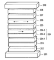
도 8은 제9 실시예의 자기저항 효과 소자를 도시한다. 도 8에서, 본 실시예의 자기저항 효과 소자는, 제1 전극(201); 5 nm의 Ta 층 및 2 nm의 Ru 층을 포함하는 기판층(202); 약 15 nm의 두께로 PtMn으로부터 형성된 반강자성층(203); 3 내지 4 nm 정도의 두께로 Co90Fe10으로부터 형성된 제1 자화 고착층(204-1), 약 0.9 nm 정도의 두께로 Ru로부터 형성된 자화 반평행 결합층(204-2), 및 Co90Fe10 층으로부터 형성된 제2 자화 고착층(204-3)을 포함하는 자화 고착층(204); 약 3 nm의 두께로 Cu로부터 형성된 스페이서층(205); Co90Fe10 층으로부터 형성된 자화 자유층(206); 약 1nm의 두께로 Cu로부터 형성된 제1 보호층(207); 약 5 nm의 두께로 Ru로부터 형성된 제2 보호층(208); 및 제2 전극(209)을 적층한 구조를 갖는다.8 shows the magnetoresistive effect element of the ninth embodiment. In Fig. 8, the magnetoresistive effect element of this embodiment includes: a
기능층(210-1)은 제2 자화 고착층(204-3)과 스페이서층(205) 사이의 경계를 따라 존재하고, 기능층(210-2)은 자화 자유층(206)과 스페이서층(205) 사이의 경계를 따라 존재한다. 제2 자화 고착층(204-3) 및 기능층(210-1)의 전체 두께는 약 3 nm이고, 자화 자유층(206) 및 기능층(210-2)의 전체 두께는 약 3 nm이다.The functional layer 210-1 exists along the boundary between the second magnetization fixing layer 204-3 and the
도 20에 도시된 바와 같이, 표 9는 자화 고착층에 기능층이 제공되는 자기저항 효과 소자에서 얻어진 MR 비, 및 자화 고착층과 스페이서층 사이의 경계를 따라 기능층이 존재하는 자기저항 효과 소자에서 얻어진 MR 비의 크기 사이의 비교를 도시한다. 제1 실시예에서 이용된 Fe의 산화물층이 기능층에 적용된다. 제1 실시예의 샘플 그룹들 A-1 내지 A-4 및 B-1 내지 B-4에 대하여 이용되는 산화 조건들, AIT 조건들, 등이 그대로 이용된다.As shown in FIG. 20, Table 9 shows the MR ratio obtained in the magnetoresistive element in which the functional layer is provided in the magnetized layer, and the magnetoresistive element in which the functional layer exists along the boundary between the magnetized layer and the spacer layer. The comparison between the magnitudes of the MR ratios obtained is shown. An oxide layer of Fe used in the first embodiment is applied to the functional layer. Oxidation conditions, AIT conditions, and the like used for the sample groups A-1 to A-4 and B-1 to B-4 of the first embodiment are used as they are.
표 9에 따르면, 제2 자화 고착층(204-3)과 스페이서층(205) 사이의 경계를 따라 기능층(210-1)이 삽입되거나, 자화 자유층(206)과 스페이서층(205) 사이의 경계를 따라 기능층(210-2)이 삽입되는 경우에도, 제1 내지 제8 실시예들에서 도출된 것과 유사한 스핀 필터링 효과가 도출된다. 더욱이, 제1 내지 제8 실시예들의 경우와 같이, 도 2a - 2e에 도시된 박막 형성 프로세스를 통해 기능층들이 형성되는 샘플들(U-1, U-2, U-3, 및 U-4)의 MR 비들은, 도 2a - 2e에 도시된 바와 같은 박막 형성 프로세스를 포함하지 않는 프로세스를 통해 형성되는 기능층들을 갖는 자기저항 효과 소자의 샘플들(T-1, T-2, T-3, 및 T-4)의 MR 비들보다 더 크게 되는 것이 이해된다. 그 이유는, 제1 실시예 등과 관련하여 기술된 바와 같이, 도 2a - 2e에 도시된 프로세스로 균일한 두께를 갖는 기능층이 성장될 수 있기 때문이다.According to Table 9, the functional layer 210-1 is inserted along the boundary between the second magnetization fixing layer 204-3 and the
전술된 바와 같이, 제9 실시예에서, 제2 자화 고착층(204-3)과 스페이서층(205) 사이의 경계를 따라 기능층(210-1)이 삽입되거나, 자화 자유층(206)과 스페이서층(205) 사이의 경계를 따라 기능층(210-2)이 삽입된다. 그러나, 기능층이 두 경계들 사이에 삽입될 수 있다. 그 경우에, 제2 자화 고착층에 의한 스핀 필터링 효과와 자화 자유층에 의한 스핀 필터링 효과의 상승 효과가 나타난다. 더욱이, 보다 높은 MR 비를 갖는 자기저항 효과 소자가 제조될 수 있다.As described above, in the ninth embodiment, the functional layer 210-1 is inserted along the boundary between the second magnetization fixing layer 204-3 and the
(제10 실시예)(Example 10)
전술된 실시예들 모두 GMR 구조의 자기저항 효과 소자들에 관한 것이지만, 본 발명은 GMR 구조로 한정되는 것은 아니며, TMR 구조에도 적용될 수 있다. 본 실시예에서는, 기능층이 TMR 구조로부터 형성되는 자기저항 효과 소자가 도시된다. TMR 구조에서, GMR 구조의 기능층은 배리어층에 상당한다. TMR 구조의 자기저항 효과 소자는 현재 하드 디스크 드라이브의 재생 헤드의 RA의 감소의 문제가 있다. 더 낮은 RA를 얻기 위하여, 배리어층의 두께가 감소되어야 한다. 또한, 배리어층의 두께가 감소되는 경우, 배리어층에서의 핀홀들의 형성 및 MR의 심각한 감소의 문제를 야기시킨다.Although the above-described embodiments all relate to magnetoresistive effect elements of a GMR structure, the present invention is not limited to the GMR structure, but may also be applied to a TMR structure. In this embodiment, a magnetoresistive element in which the functional layer is formed from the TMR structure is shown. In the TMR structure, the functional layer of the GMR structure corresponds to the barrier layer. The magnetoresistive effect element of the TMR structure currently has a problem of reducing the RA of the playhead of the hard disk drive. In order to obtain lower RA, the thickness of the barrier layer must be reduced. In addition, when the thickness of the barrier layer is reduced, it causes a problem of the formation of pinholes in the barrier layer and a serious reduction of the MR.
도 10에서, 본 실시예의 자기저항 효과 소자는, 제1 전극(201); 5 nm의 Ta 층 및 2 nm의 Ru 층을 포함하는 기판층(202); 15 nm 두께로 PtMn으로부터 형성된 반강자성층(203); 3 내지 4 nm 정도의 두께로 Co90Fe10로부터 형성된 제1 자화 고착층(204-1), 약 0.9 nm 정도의 두께로 Ru로부터 형성된 자화 반평행 결합층(204-2), 및 2 nm 정도의 두께로 Co90Fe10 층으로부터 형성된 제2 자화 고착층(204-3)을 포함하는 자화 고착층(204); AlO로부터 형성된 배리어층(211); 약 2 nm의 Co75Fe25 층 및 3.5 nm의 Ni80Fe20 층을 갖는 2층 구조를 갖는 자화 자유층(206); 약 1 nm의 두께로 Cu로부터 형성된 제1 보호층(207); 약 5 nm의 두께로 Ru로부터 형성된 제2 보호층(8); 및 제2 전극(9)을 적층한 구조를 갖는다.In Fig. 10, the magnetoresistive effect element of this embodiment includes: a
도 21에 도시된 표 10은 배리어층(211)을 형성하기 위한 프로세스들을 도시한다.Table 10 shown in FIG. 21 shows processes for forming the barrier layer 211.
표 10은 도 2a - 2e에 도시된 프로세스들을 통하여 배리어층들이 형성되는 샘플들 w-1, w-2, w-3, 및 w-4 모두는 시작으로부터 두꺼운 AlO로부터 형성된 샘플들 V-1, V-2, V-3, 및 V-4에 의하여 보여지는 것들 보다 더 큰 MR 비들을 나타낸다. 그 이유는 핀홀들의 수가 감소되고 균일한 배리어층이 생성되기 때문이다.Table 10 shows that the samples w-1, w-2, w-3, and w-4 in which the barrier layers are formed through the processes shown in FIGS. 2A-2E are all samples V-1, formed from thick AlO from the beginning, MR ratios greater than those shown by V-2, V-3, and V-4. This is because the number of pinholes is reduced and a uniform barrier layer is created.
제10 실시예에서, 배리어층은 Al의 산화물로서 간주된다. 그러나, 배리어층은 이 재료에 한정되는 것은 아니다. 배리어층에 대한 필수 요건은, Fe, Co, Ni, Cu, Ti, V, Cr, Mn, Mg, Al, Si, Zr, Nb, Mo, Ru, Rh, Pd, Ag, Hf, Ta, W, Re, Ir, Pt, 및 Au를 포함하는 그룹으로부터 선택된 적어도 하나를 포함하는 금속 또는 합금을 산화, 질화, 또는 플루오르화(fluorinating)시킴으로써 형성된 산화물, 질화 물, 또는 플루오르화물(fluoride)로 되는 것이다. 이 경우에도, 배리어층은 박막 형성 프로세스를 통하여 균일하게 될 수 있다.In the tenth embodiment, the barrier layer is regarded as an oxide of Al. However, the barrier layer is not limited to this material. Essential requirements for the barrier layer are Fe, Co, Ni, Cu, Ti, V, Cr, Mn, Mg, Al, Si, Zr, Nb, Mo, Ru, Rh, Pd, Ag, Hf, Ta, W, Oxides, nitrides, or fluorides formed by oxidizing, nitriding, or fluorinating a metal or alloy comprising at least one selected from the group comprising Re, Ir, Pt, and Au. Even in this case, the barrier layer can be made uniform through the thin film forming process.
제10 실시예에서, 배리어층은 본 발명의 프로세스들을 거친다. 제1 내지 제9 실시예들의 경우에서와 같이, 본 발명은 또한 자화 고착층 또는 자화 자유층에 삽입되는 기능층을 형성하는 프로세스로서 자연스럽게 적용된다.In a tenth embodiment, the barrier layer is subjected to the processes of the present invention. As in the case of the first through ninth embodiments, the present invention also naturally applies as a process of forming a functional layer to be inserted into a magnetized anchoring layer or a magnetized free layer.
본 발명은 설명된 실시예들에 한정되는 것은 아니다. 실제 단계에서, 본 발명의 요지로부터 벗어나지 않고 변형되면서 구성 요소들이 구현될 수 있다. 본 실시예들에서 기술된 복수의 구성 요소들의 적절한 조합에 의하여 다양한 발명들이 생성될 수 있다. 예를 들면, 일부 구성 요소들은 상기 실시예들에 기술된 구성 요소들 모두로부터 제거될 수 있다. 더욱이, 상이한 실시예들에 기술된 구성 요소들은 또한 적절하게 조합될 수 있다.The invention is not limited to the described embodiments. In actual steps, components may be implemented with modifications without departing from the spirit of the invention. Various inventions can be produced by an appropriate combination of a plurality of components described in the present embodiments. For example, some components may be removed from all of the components described in the above embodiments. Moreover, the components described in the different embodiments can also be combined as appropriate.
도 1은 본 발명의 제1 내지 제8 실시예에 따른 자기저항효과소자의 구조도이다.1 is a structural diagram of a magnetoresistive element according to the first to eighth embodiments of the present invention.
도 2a-2e는 본 발명의 기능층 및 배리어층의 형성에 관한 도면들이다.2A-2E illustrate the formation of a functional layer and a barrier layer of the present invention.
도 3은 본 발명의 프로세스를 통하여 작성된 기능층의 스핀 필터링 효과를 보여주는 도면이다.3 is a view showing the spin filtering effect of the functional layer created through the process of the present invention.
도 4는 본 발명의 제1 실시예의 제1 변형예에 따른 자기저항효과소자의 구조도이다.4 is a structural diagram of a magnetoresistive element according to a first modification of the first embodiment of the present invention.
도 5는 본 발명의 제1 실시예의 제2 변형예에 따른 자기저항효과소자의 구조도이다.5 is a structural diagram of a magnetoresistive element according to a second modification of the first embodiment of the present invention.
도 6a 및 6b는 본 발명의 프로세스를 통하여 작성된 기능층의 TEM 이미지와 종래의 프로세스를 통하여 작성된 기능층의 TEM 이미지를 각각 보여준다.6A and 6B show TEM images of functional layers created through the process of the present invention and TEM images of functional layers created through the conventional process, respectively.
도 7은 본 발명의 프로세스 중의 AIT 처리에서의 인가된 전압과 MR 비 간의 상관 관계를 보여주는 그래프이다.7 is a graph showing the correlation between the applied voltage and MR ratio in AIT processing during the process of the present invention.
도 8은 본 발명의 제9 실시예에 따른 자기저항효과소자의 구조도이다.8 is a structural diagram of a magnetoresistive element according to a ninth embodiment of the present invention.
도 9는 본 발명의 제7 실시예에 따른 자기저항효과소자의 구조도이다.9 is a structural diagram of a magnetoresistive element according to a seventh embodiment of the present invention.
도 10은 본 발명의 제10 실시예에 따른 자기저항효과소자의 구조도이다.10 is a structural diagram of a magnetoresistive element according to a tenth embodiment of the present invention.
도 11은 종래의 프로세스를 통하여 작성된 기능층의 스핀 필터링 효과를 보여주는 도면이다.11 is a diagram illustrating spin filtering effects of a functional layer created through a conventional process.
도 12는 실시예에 따라서 제작된 샘플들에 대한 프로세스 필요 조건들을 보 여주는 표이다.12 is a table showing process requirements for samples fabricated in accordance with an embodiment.
도 13은 실시예에 따라서 제작된 샘플들에 대한 프로세스 필요 조건들을 보여주는 표이다.13 is a table showing process requirements for samples fabricated in accordance with an embodiment.
도 14는 실시예에 따라서 제작된 샘플들에 대한 프로세스 필요 조건들을 보여주는 표이다.14 is a table showing process requirements for samples fabricated in accordance with an embodiment.
도 15는 실시예에 따라서 제작된 샘플들에 대한 프로세스 필요 조건들을 보여주는 표이다.15 is a table showing process requirements for samples fabricated in accordance with an embodiment.
도 16은 실시예에 따라서 제작된 샘플들에 대한 프로세스 필요 조건들을 보여주는 표이다.16 is a table showing process requirements for samples fabricated in accordance with an embodiment.
도 17은 샘플들에 대한 MR 비의 측정 결과를 보여주는 표이다.17 is a table showing measurement results of MR ratios for samples.
도 18은 샘플들에 대한 MR 비의 측정 결과를 보여주는 표이다.18 is a table showing measurement results of MR ratios for samples.
도 19는 샘플들에 대한 MR 비의 측정 결과를 보여주는 표이다.19 is a table showing measurement results of MR ratios for samples.
도 20은 자기저항효과소자의 샘플들에서 얻어진 MR 비의 크기 간의 비교를 보여주는 표이다.20 is a table showing a comparison between the magnitudes of the MR ratios obtained in the samples of the magnetoresistive element.
도 21은 실시예에 따라서 제작된 샘플들에 대한 프로세스 필요 조건들을 보여주는 표이다.21 is a table showing process requirements for samples made according to the embodiment.
<도면의 주요 부분에 대한 부호의 설명><Explanation of symbols for main parts of the drawings>
1 : 제1 전극1: first electrode
2 : 기판층2: substrate layer
3 : 반강자성층3: antiferromagnetic layer
4 : 자화 고착층4: magnetization fixing layer
5 : 스페이서 층5: spacer layer
6 : 자화 자유층6: magnetization free layer
7 : 제1 보호층7: first protective layer
8 : 제2 보호층8: second protective layer
9 : 제2 전극9: second electrode
Claims (7)
Applications Claiming Priority (2)
| Application Number | Priority Date | Filing Date | Title |
|---|---|---|---|
| JPJP-P-2006-032261 | 2006-02-09 | ||
| JP2006032261A JP4514721B2 (en) | 2006-02-09 | 2006-02-09 | Magnetoresistive element manufacturing method, magnetoresistive element, magnetoresistive head, magnetic recording / reproducing apparatus, and magnetic storage apparatus |
Related Parent Applications (1)
| Application Number | Title | Priority Date | Filing Date |
|---|---|---|---|
| KR1020070013222A Division KR100912154B1 (en) | 2006-02-09 | 2007-02-08 | Method for manufacturing magnetoresistance effect element |
Publications (2)
| Publication Number | Publication Date |
|---|---|
| KR20080098479A true KR20080098479A (en) | 2008-11-10 |
| KR100922247B1 KR100922247B1 (en) | 2009-10-15 |
Family
ID=38444324
Family Applications (2)
| Application Number | Title | Priority Date | Filing Date |
|---|---|---|---|
| KR1020070013222A Expired - Fee Related KR100912154B1 (en) | 2006-02-09 | 2007-02-08 | Method for manufacturing magnetoresistance effect element |
| KR1020080104637A Expired - Fee Related KR100922247B1 (en) | 2006-02-09 | 2008-10-24 | Method for manufacturing magnetoresistance effect element |
Family Applications Before (1)
| Application Number | Title | Priority Date | Filing Date |
|---|---|---|---|
| KR1020070013222A Expired - Fee Related KR100912154B1 (en) | 2006-02-09 | 2007-02-08 | Method for manufacturing magnetoresistance effect element |
Country Status (4)
| Country | Link |
|---|---|
| US (1) | US7897201B2 (en) |
| JP (1) | JP4514721B2 (en) |
| KR (2) | KR100912154B1 (en) |
| CN (1) | CN101017668A (en) |
Families Citing this family (21)
| Publication number | Priority date | Publication date | Assignee | Title |
|---|---|---|---|---|
| JP4786331B2 (en) | 2005-12-21 | 2011-10-05 | 株式会社東芝 | Method for manufacturing magnetoresistive element |
| JP4514721B2 (en) | 2006-02-09 | 2010-07-28 | 株式会社東芝 | Magnetoresistive element manufacturing method, magnetoresistive element, magnetoresistive head, magnetic recording / reproducing apparatus, and magnetic storage apparatus |
| JP2007299880A (en) | 2006-04-28 | 2007-11-15 | Toshiba Corp | Magnetoresistive element and method of manufacturing magnetoresistive element |
| JP4550777B2 (en) | 2006-07-07 | 2010-09-22 | 株式会社東芝 | Magnetoresistive element manufacturing method, magnetoresistive element, magnetic head, magnetic recording / reproducing apparatus, and magnetic memory |
| JP5044157B2 (en) * | 2006-07-11 | 2012-10-10 | 株式会社東芝 | Magnetoresistive element, magnetic head, and magnetic reproducing apparatus |
| JP4388093B2 (en) | 2007-03-27 | 2009-12-24 | 株式会社東芝 | Magnetoresistive element, magnetic head, magnetic recording / reproducing apparatus |
| US7932571B2 (en) * | 2007-10-11 | 2011-04-26 | Everspin Technologies, Inc. | Magnetic element having reduced current density |
| JP5361201B2 (en) | 2008-01-30 | 2013-12-04 | 株式会社東芝 | Method for manufacturing magnetoresistive element |
| JP5150284B2 (en) | 2008-01-30 | 2013-02-20 | 株式会社東芝 | Magnetoresistive element and manufacturing method thereof |
| JP5039006B2 (en) | 2008-09-26 | 2012-10-03 | 株式会社東芝 | Magnetoresistive element manufacturing method, magnetoresistive element, magnetic head assembly, and magnetic recording / reproducing apparatus |
| JP5032429B2 (en) * | 2008-09-26 | 2012-09-26 | 株式会社東芝 | Magnetoresistive element manufacturing method, magnetoresistive element, magnetic head assembly, and magnetic recording / reproducing apparatus |
| JP5039007B2 (en) | 2008-09-26 | 2012-10-03 | 株式会社東芝 | Magnetoresistive element manufacturing method, magnetoresistive element, magnetic head assembly, and magnetic recording / reproducing apparatus |
| JP5032430B2 (en) * | 2008-09-26 | 2012-09-26 | 株式会社東芝 | Magnetoresistive element manufacturing method, magnetoresistive element, magnetic head assembly, and magnetic recording / reproducing apparatus |
| JP2010080839A (en) | 2008-09-29 | 2010-04-08 | Toshiba Corp | Method of manufacturing magneto-resistance effect device, the magneto-resistance effect device, magnetic head assembly, and magnetic recording and reproducing apparatus |
| JP4991901B2 (en) * | 2010-04-21 | 2012-08-08 | 株式会社東芝 | Magnetoresistive element and magnetic recording / reproducing apparatus |
| JP4991920B2 (en) * | 2010-09-01 | 2012-08-08 | 株式会社東芝 | Method for manufacturing magnetoresistive element |
| JP5629608B2 (en) * | 2011-02-25 | 2014-11-26 | 株式会社東芝 | Magnetoresistive element, magnetic head assembly, magnetic recording / reproducing apparatus, memory cell array, and method of manufacturing magnetoresistive element |
| US8884386B2 (en) * | 2012-02-02 | 2014-11-11 | Taiwan Semiconductor Manufacturing Company, Ltd. | MRAM device and fabrication method thereof |
| KR20130138137A (en) * | 2012-06-08 | 2013-12-18 | 주식회사 엘지화학 | High flux reverse osmosis membrane comprising surface treated zeolite and manufacturing method thereof |
| CA2958388A1 (en) | 2016-04-27 | 2017-10-27 | Rolls-Royce Corporation | Supercritical transient storage of refrigerant |
| JP7202267B2 (en) * | 2019-08-06 | 2023-01-11 | 株式会社日立ハイテク | Magnetoresistive element and magnetoresistive device |
Family Cites Families (150)
| Publication number | Priority date | Publication date | Assignee | Title |
|---|---|---|---|---|
| US5304975A (en) * | 1991-10-23 | 1994-04-19 | Kabushiki Kaisha Toshiba | Magnetoresistance effect element and magnetoresistance effect sensor |
| FR2685489B1 (en) * | 1991-12-23 | 1994-08-05 | Thomson Csf | LOW MAGNETIC FIELD SENSOR WITH MAGNETORESISTIVE EFFECT. |
| US5448515A (en) | 1992-09-02 | 1995-09-05 | Mitsubishi Denki Kabushiki Kaisha | Magnetic thin film memory and recording/reproduction method therefor |
| US5549978A (en) | 1992-10-30 | 1996-08-27 | Kabushiki Kaisha Toshiba | Magnetoresistance effect element |
| US5780176A (en) * | 1992-10-30 | 1998-07-14 | Kabushiki Kaisha Toshiba | Magnetoresistance effect element |
| JP3184352B2 (en) | 1993-02-18 | 2001-07-09 | 松下電器産業株式会社 | Memory element |
| EP0629998A2 (en) * | 1993-06-18 | 1994-12-21 | International Business Machines Corporation | Magnetoresistive film, method of its fabrication and magnetoresistive sensor |
| JPH08504303A (en) * | 1993-10-06 | 1996-05-07 | フィリップス エレクトロニクス ネムローゼ フェン ノートシャップ | Magnetoresistive device and magnetic head using such device |
| US6002553A (en) | 1994-02-28 | 1999-12-14 | The United States Of America As Represented By The United States Department Of Energy | Giant magnetoresistive sensor |
| US5583725A (en) | 1994-06-15 | 1996-12-10 | International Business Machines Corporation | Spin valve magnetoresistive sensor with self-pinned laminated layer and magnetic recording system using the sensor |
| US5874886A (en) * | 1994-07-06 | 1999-02-23 | Tdk Corporation | Magnetoresistance effect element and magnetoresistance device |
| DE69611804D1 (en) | 1995-04-17 | 2001-03-29 | Read Rite Corp | Formation of an insulating thin film by a large number of ion beams |
| US5777542A (en) * | 1995-08-28 | 1998-07-07 | Kabushiki Kaisha Toshiba | Magnetoresistance effect device and manufacturing method thereof |
| WO1997011499A1 (en) * | 1995-09-21 | 1997-03-27 | Tdk Corporation | Magnetic transducer |
| FR2742571B1 (en) * | 1995-12-15 | 1998-01-16 | Commissariat Energie Atomique | MULTI-LAYERED STRUCTURE AND SENSOR AND METHOD FOR PRODUCING THE SAME |
| JP3293437B2 (en) * | 1995-12-19 | 2002-06-17 | 松下電器産業株式会社 | Magnetoresistive element, magnetoresistive head and memory element |
| US6084752A (en) * | 1996-02-22 | 2000-07-04 | Matsushita Electric Industrial Co., Ltd. | Thin film magnetic head |
| TW367493B (en) | 1996-04-30 | 1999-08-21 | Toshiba Corp | Reluctance component |
| US5668688A (en) | 1996-05-24 | 1997-09-16 | Quantum Peripherals Colorado, Inc. | Current perpendicular-to-the-plane spin valve type magnetoresistive transducer |
| JPH11510911A (en) | 1996-06-12 | 1999-09-21 | フィリップス エレクトロニクス ネムローゼ フェンノートシャップ | Magnetoresistive magnetic field sensor |
| US5768183A (en) * | 1996-09-25 | 1998-06-16 | Motorola, Inc. | Multi-layer magnetic memory cells with improved switching characteristics |
| US5768181A (en) * | 1997-04-07 | 1998-06-16 | Motorola, Inc. | Magnetic device having multi-layer with insulating and conductive layers |
| DE69820524T2 (en) | 1997-05-09 | 2004-09-23 | Kabushiki Kaisha Toshiba, Kawasaki | Magnetic element and magnetic head or memory element using this element |
| JP3472087B2 (en) | 1997-06-30 | 2003-12-02 | Tdk株式会社 | Film structure, electronic device, recording medium, and method for producing oxide conductive thin film |
| JP3182399B2 (en) | 1997-09-17 | 2001-07-03 | 株式会社東芝 | Soft magnetic alloy film and manufacturing method thereof, magnetic head, and magnetic disk |
| DE69827737D1 (en) | 1997-09-29 | 2004-12-30 | Matsushita Electric Industrial Co Ltd | Magnetoresistance effect device, magnetoresistive head and method of manufacturing a magnetoresistance effect device |
| US6033584A (en) * | 1997-12-22 | 2000-03-07 | Advanced Micro Devices, Inc. | Process for reducing copper oxide during integrated circuit fabrication |
| JP3679593B2 (en) * | 1998-01-28 | 2005-08-03 | キヤノン株式会社 | Magnetic thin film element, magnetic thin film memory element and recording / reproducing method thereof |
| US6303218B1 (en) | 1998-03-20 | 2001-10-16 | Kabushiki Kaisha Toshiba | Multi-layered thin-film functional device and magnetoresistance effect element |
| JP4409656B2 (en) | 1998-03-20 | 2010-02-03 | 株式会社東芝 | Magnetoresistive element and magnetic reproducing apparatus |
| US6313973B1 (en) | 1998-06-30 | 2001-11-06 | Kabushiki Kaisha Toshiba | Laminated magnetorestrictive element of an exchange coupling film, an antiferromagnetic film and a ferromagnetic film and a magnetic disk drive using same |
| JP3234814B2 (en) | 1998-06-30 | 2001-12-04 | 株式会社東芝 | Magnetoresistive element, magnetic head, magnetic head assembly, and magnetic recording device |
| JP2000091667A (en) * | 1998-09-09 | 2000-03-31 | Read Rite Smi Kk | Spin valve magnetoresistance sensor and thin-film magnetic head |
| JP2000099922A (en) * | 1998-09-17 | 2000-04-07 | Sony Corp | Magnetic tunnel element and method of manufacturing the same |
| US6542342B1 (en) * | 1998-11-30 | 2003-04-01 | Nec Corporation | Magnetoresistive effect transducer having longitudinal bias layer directly connected to free layer |
| JP2000228004A (en) | 1998-11-30 | 2000-08-15 | Nec Corp | Magneto-resistive element, reproducing head and recording and reproducing system |
| JP2000188435A (en) | 1998-12-22 | 2000-07-04 | Sony Corp | Magnetic tunneling junction element and method of manufacturing the same, magnetic head using the same, magnetic sensor, magnetic memory, and magnetic recording / reproducing device, magnetic sensor device, magnetic memory device |
| US6348274B1 (en) * | 1998-12-28 | 2002-02-19 | Kabushiki Kaisha Toshiba | Magnetoresistive element and magnetic recording apparatus |
| JP2000215414A (en) * | 1999-01-25 | 2000-08-04 | Hitachi Ltd | Magnetic sensor |
| US6567246B1 (en) * | 1999-03-02 | 2003-05-20 | Matsushita Electric Industrial Co., Ltd. | Magnetoresistance effect element and method for producing the same, and magnetoresistance effect type head, magnetic recording apparatus, and magnetoresistance effect memory element |
| JP3601690B2 (en) | 1999-03-02 | 2004-12-15 | 松下電器産業株式会社 | Magnetoresistive element and manufacturing method thereof, magnetoresistive head, magnetic recording device, magnetoresistive memory element |
| JP2000293982A (en) | 1999-04-08 | 2000-10-20 | Victor Co Of Japan Ltd | Magnetic memory |
| US6330137B1 (en) | 1999-06-11 | 2001-12-11 | Read-Rite Corporation | Magnetoresistive read sensor including a carbon barrier layer and method for making same |
| US6436526B1 (en) * | 1999-06-17 | 2002-08-20 | Matsushita Electric Industrial Co., Ltd. | Magneto-resistance effect element, magneto-resistance effect memory cell, MRAM and method for performing information write to or read from the magneto-resistance effect memory cell |
| US6275363B1 (en) | 1999-07-23 | 2001-08-14 | International Business Machines Corporation | Read head with dual tunnel junction sensor |
| JP2001094173A (en) | 1999-09-22 | 2001-04-06 | Fujitsu Ltd | Magnetic sensor, magnetic head and magnetic disk drive |
| KR100373473B1 (en) * | 1999-09-24 | 2003-02-25 | 가부시끼가이샤 도시바 | Magnetoresistance device, magnetoresistance head, magnetoreproducing device, and magnetic stacked body |
| US6556390B1 (en) * | 1999-10-28 | 2003-04-29 | Seagate Technology Llc | Spin valve sensors with an oxide layer utilizing electron specular scattering effect |
| JP2001143227A (en) | 1999-11-18 | 2001-05-25 | Fujitsu Ltd | Magnetic sensor |
| US6770382B1 (en) | 1999-11-22 | 2004-08-03 | Headway Technologies, Inc. | GMR configuration with enhanced spin filtering |
| JP3623417B2 (en) | 1999-12-03 | 2005-02-23 | アルプス電気株式会社 | Spin valve thin film magnetic element and thin film magnetic head |
| JP2001176027A (en) * | 1999-12-14 | 2001-06-29 | Nec Corp | Magnetoresistance effect head and magnetic memory device using the same |
| US6560077B2 (en) * | 2000-01-10 | 2003-05-06 | The University Of Alabama | CPP spin-valve device |
| US6639762B2 (en) * | 2000-01-24 | 2003-10-28 | Alps Electric Co., Ltd. | Spin valve thin-film magnetic device having free magnetic layer in ferrimagnetic state and manufacturing method therefor |
| JP2001216612A (en) | 2000-01-31 | 2001-08-10 | Alps Electric Co Ltd | Spin valve type thin film magnetic element and thin film magnetic head provided with the same |
| JP2001229511A (en) | 2000-02-10 | 2001-08-24 | Fujitsu Ltd | Magnetoresistive film, magnetoresistive head, information reproducing apparatus, and method of manufacturing magnetoresistive film |
| US6353318B1 (en) * | 2000-03-10 | 2002-03-05 | Read-Rite Corporation | Magnetoresistive sensor having hard biased current perpendicular to the plane sensor |
| US6603642B1 (en) | 2000-03-15 | 2003-08-05 | Tdk Corporation | Magnetic transducer having a plurality of magnetic layers stacked alternately with a plurality of nonmagnetic layers and a fixed-orientation-of-magnetization layer and thin film magnetic head including the magnetic transducer |
| US6469926B1 (en) | 2000-03-22 | 2002-10-22 | Motorola, Inc. | Magnetic element with an improved magnetoresistance ratio and fabricating method thereof |
| JP3462832B2 (en) | 2000-04-06 | 2003-11-05 | 株式会社日立製作所 | Magnetic resistance sensor, magnetic head and magnetic recording / reproducing apparatus using the same |
| US6522507B1 (en) * | 2000-05-12 | 2003-02-18 | Headway Technologies, Inc. | Single top spin valve heads for ultra-high recording density |
| US6452763B1 (en) | 2000-06-06 | 2002-09-17 | International Business Machines Corporation | GMR design with nano oxide layer in the second anti-parallel pinned layer |
| US6473275B1 (en) | 2000-06-06 | 2002-10-29 | International Business Machines Corporation | Dual hybrid magnetic tunnel junction/giant magnetoresistive sensor |
| JP2001358380A (en) | 2000-06-13 | 2001-12-26 | Alps Electric Co Ltd | Spin-valve thin-film magnetic element and thin-film magnetic head provided with the element |
| US6517896B1 (en) | 2000-08-07 | 2003-02-11 | Headway Technologies, Inc. | Spin filter bottom spin valve head with continuous spacer exchange bias |
| US6767655B2 (en) | 2000-08-21 | 2004-07-27 | Matsushita Electric Industrial Co., Ltd. | Magneto-resistive element |
| US6853520B2 (en) * | 2000-09-05 | 2005-02-08 | Kabushiki Kaisha Toshiba | Magnetoresistance effect element |
| JP3559513B2 (en) * | 2000-09-05 | 2004-09-02 | 株式会社東芝 | Magnetoresistive element, method and apparatus for manufacturing the same, and magnetic reproducing apparatus |
| JP3618654B2 (en) * | 2000-09-11 | 2005-02-09 | 株式会社東芝 | Magnetoresistive element, magnetic head, and magnetic recording / reproducing apparatus |
| JP3833512B2 (en) | 2000-10-20 | 2006-10-11 | 株式会社東芝 | Magnetoresistive effect element |
| JP4896587B2 (en) | 2000-10-20 | 2012-03-14 | 株式会社東芝 | Magnetoresistive element, magnetic head, and magnetic reproducing apparatus |
| US6937446B2 (en) * | 2000-10-20 | 2005-08-30 | Kabushiki Kaisha Toshiba | Magnetoresistance effect element, magnetic head and magnetic recording and/or reproducing system |
| JP2002150512A (en) | 2000-11-08 | 2002-05-24 | Sony Corp | Magnetoresistive element and magnetoresistive head |
| US7059201B2 (en) * | 2000-12-20 | 2006-06-13 | Fidelica Microsystems, Inc. | Use of multi-layer thin films as stress sensors |
| US6771473B2 (en) | 2001-01-22 | 2004-08-03 | Matsushita Electric Industrial Co., Ltd. | Magnetoresistive element and method for producing the same |
| US6809900B2 (en) | 2001-01-25 | 2004-10-26 | Seagate Technology Llc | Write head with magnetization controlled by spin-polarized electron current |
| US6905780B2 (en) * | 2001-02-01 | 2005-06-14 | Kabushiki Kaisha Toshiba | Current-perpendicular-to-plane-type magnetoresistive device, and magnetic head and magnetic recording-reproducing apparatus using the same |
| JP2004022614A (en) * | 2002-06-13 | 2004-01-22 | Alps Electric Co Ltd | Magnetic sensor element and method of manufacturing the same |
| US6992869B2 (en) | 2001-02-06 | 2006-01-31 | Yamaha Corporation | Magnetic resistance device |
| US6686068B2 (en) * | 2001-02-21 | 2004-02-03 | International Business Machines Corporation | Heterogeneous spacers for CPP GMR stacks |
| US6704175B2 (en) | 2001-03-28 | 2004-03-09 | Tdk Corporation | Current perpendicular-to-the-plane magnetoresistance read head |
| JP3590006B2 (en) * | 2001-06-22 | 2004-11-17 | 株式会社東芝 | Magnetoresistive element, magnetic head, and magnetic reproducing device |
| US6636389B2 (en) * | 2001-08-03 | 2003-10-21 | International Business Machines Corporation | GMR magnetic transducer with nano-oxide exchange coupled free layers |
| JP2003086866A (en) | 2001-09-13 | 2003-03-20 | Anelva Corp | Manufacturing method of giant magnetoresistive thin film of spin valve type |
| JP3958947B2 (en) * | 2001-09-14 | 2007-08-15 | アルプス電気株式会社 | Magnetic sensing element and manufacturing method thereof |
| US6888703B2 (en) | 2001-09-17 | 2005-05-03 | Headway Technologies, Inc. | Multilayered structures comprising magnetic nano-oxide layers for current perpindicular to plane GMR heads |
| JP3967237B2 (en) | 2001-09-19 | 2007-08-29 | 株式会社東芝 | Magnetoresistive element, method for manufacturing the same, magnetic reproducing element, and magnetic memory |
| US6937447B2 (en) * | 2001-09-19 | 2005-08-30 | Kabushiki Kaisha Toshiba | Magnetoresistance effect element, its manufacturing method, magnetic reproducing element and magnetic memory |
| JP2003110168A (en) * | 2001-10-01 | 2003-04-11 | Alps Electric Co Ltd | Magnetic detection device and method for its manufacture |
| FR2830971B1 (en) | 2001-10-12 | 2004-03-12 | Commissariat Energie Atomique | MAGNETORESISTIVE DEVICE WITH IMPROVED PERFORMANCE SPIN VALVE |
| KR200262282Y1 (en) * | 2001-10-19 | 2002-03-18 | 박우희 | Water cabinet |
| JP2003162806A (en) * | 2001-11-27 | 2003-06-06 | Hitachi Ltd | Perpendicular magnetic recording medium and magnetic storage device |
| JP2003198004A (en) * | 2001-12-27 | 2003-07-11 | Fujitsu Ltd | Magnetoresistance effect element |
| JP4184668B2 (en) | 2002-01-10 | 2008-11-19 | 富士通株式会社 | CPP structure magnetoresistive effect element |
| JP3749873B2 (en) * | 2002-03-28 | 2006-03-01 | 株式会社東芝 | Magnetoresistive element, magnetic head, and magnetic reproducing apparatus |
| JP4382333B2 (en) * | 2002-03-28 | 2009-12-09 | 株式会社東芝 | Magnetoresistive element, magnetic head, and magnetic reproducing apparatus |
| JP2004031545A (en) | 2002-06-25 | 2004-01-29 | Alps Electric Co Ltd | Magnetic detector and its manufacturing method |
| JP2004095110A (en) | 2002-09-03 | 2004-03-25 | Hitachi Ltd | Spin valve type magnetic head having partial current confinement layer, method for manufacturing the same, and current confinement method |
| JP3648504B2 (en) | 2002-09-06 | 2005-05-18 | 株式会社東芝 | Magnetoresistive element, magnetic head, and magnetic reproducing apparatus |
| JP4435521B2 (en) | 2002-09-11 | 2010-03-17 | 株式会社東芝 | Method for manufacturing magnetoresistive element |
| US7218484B2 (en) | 2002-09-11 | 2007-05-15 | Kabushiki Kaisha Toshiba | Magnetoresistance effect element, magnetic head, and magnetic reproducing apparatus |
| JP4284049B2 (en) * | 2002-09-25 | 2009-06-24 | 株式会社日立グローバルストレージテクノロジーズ | Magnetoresistive sensor, magnetoresistive head and manufacturing method thereof |
| JP3836788B2 (en) | 2002-12-26 | 2006-10-25 | 株式会社東芝 | Magnetoresistive element, magnetoresistive head, and magnetic recording / reproducing apparatus |
| US6800565B2 (en) * | 2003-01-13 | 2004-10-05 | Veeco Instruments, Inc. | Method of forming thin oxidation layer by cluster ion beam |
| JP3673796B2 (en) * | 2003-01-14 | 2005-07-20 | Tdk株式会社 | Magnetoresistive element manufacturing method, magnetic head, head suspension assembly, and magnetic disk apparatus |
| US6929957B2 (en) | 2003-09-12 | 2005-08-16 | Headway Technologies, Inc. | Magnetic random access memory designs with patterned and stabilized magnetic shields |
| JP4336753B2 (en) * | 2003-09-26 | 2009-09-30 | 富山県 | Ultra-thin film fabrication method |
| JP3954553B2 (en) * | 2003-09-30 | 2007-08-08 | 富士通株式会社 | Recording medium and manufacturing method thereof |
| JP2005116703A (en) * | 2003-10-06 | 2005-04-28 | Alps Electric Co Ltd | Magnetic detecting element |
| JP2005136309A (en) * | 2003-10-31 | 2005-05-26 | Toshiba Corp | Magnetoresistive element, magnetic head, head suspension assembly, magnetic reproducing apparatus, magnetoresistive element manufacturing method, and magnetoresistive element manufacturing apparatus |
| US20050141148A1 (en) * | 2003-12-02 | 2005-06-30 | Kabushiki Kaisha Toshiba | Magnetic memory |
| JP2005166896A (en) | 2003-12-02 | 2005-06-23 | Toshiba Corp | Magnetic memory |
| JP4776164B2 (en) | 2003-12-25 | 2011-09-21 | 株式会社東芝 | Magnetoresistive element, magnetic head, magnetic reproducing device, and magnetic memory |
| JP3993175B2 (en) | 2004-02-26 | 2007-10-17 | 株式会社東芝 | Current confinement type vertical energization GMR head assembly, magnetic recording / reproducing apparatus, and method for specifying proper sense current direction of current confinement type vertical energization GMR head |
| US7390529B2 (en) | 2004-05-26 | 2008-06-24 | Headway Technologies, Inc. | Free layer for CPP GMR having iron rich NiFe |
| JP2005353236A (en) | 2004-06-14 | 2005-12-22 | Fujitsu Ltd | Magnetic recording medium, method for manufacturing the same, and magnetic storage device |
| KR200373473Y1 (en) * | 2004-06-15 | 2005-01-15 | 김청용 | Burlap bag manufacture heald polishing device |
| US7611912B2 (en) | 2004-06-30 | 2009-11-03 | Headway Technologies, Inc. | Underlayer for high performance magnetic tunneling junction MRAM |
| US7331100B2 (en) * | 2004-07-07 | 2008-02-19 | Headway Technologies, Inc. | Process of manufacturing a seed/AFM combination for a CPP GMR device |
| US7576956B2 (en) * | 2004-07-26 | 2009-08-18 | Grandis Inc. | Magnetic tunnel junction having diffusion stop layer |
| JP2006049426A (en) | 2004-08-02 | 2006-02-16 | Toshiba Corp | Magnetoresistive element, method of manufacturing the same, and magnetic head and magnetic reproducing apparatus using the same |
| JP4822680B2 (en) | 2004-08-10 | 2011-11-24 | 株式会社東芝 | Method for manufacturing magnetoresistive element |
| JP4594679B2 (en) * | 2004-09-03 | 2010-12-08 | 株式会社東芝 | Magnetoresistive element, magnetic head, magnetic recording / reproducing apparatus, and magnetic memory |
| JP5095076B2 (en) | 2004-11-09 | 2012-12-12 | 株式会社東芝 | Magnetoresistive effect element |
| US20060114620A1 (en) * | 2004-11-30 | 2006-06-01 | Tdk Corporation | Granular type free layer and magnetic head |
| JP4521316B2 (en) | 2005-05-26 | 2010-08-11 | 株式会社東芝 | Magnetoresistive element, magnetic head, and magnetic recording / reproducing apparatus |
| US7583481B2 (en) * | 2005-09-23 | 2009-09-01 | Headway Technologies, Inc. | FCC-like trilayer AP2 structure for CPP GMR EM improvement |
| JP4550713B2 (en) * | 2005-10-21 | 2010-09-22 | 株式会社東芝 | Method for manufacturing magnetoresistive element |
| JP4786331B2 (en) * | 2005-12-21 | 2011-10-05 | 株式会社東芝 | Method for manufacturing magnetoresistive element |
| JP4864464B2 (en) | 2006-01-11 | 2012-02-01 | 株式会社東芝 | Magnetoresistive element, manufacturing method thereof, magnetic head, magnetic reproducing apparatus and magnetic memory using the same |
| KR100790978B1 (en) | 2006-01-24 | 2008-01-02 | 삼성전자주식회사 | Bonding method at low temperature, and semiconductor package mounting method using same |
| JP4514721B2 (en) | 2006-02-09 | 2010-07-28 | 株式会社東芝 | Magnetoresistive element manufacturing method, magnetoresistive element, magnetoresistive head, magnetic recording / reproducing apparatus, and magnetic storage apparatus |
| US7610674B2 (en) | 2006-02-13 | 2009-11-03 | Headway Technologies, Inc. | Method to form a current confining path of a CPP GMR device |
| US7599157B2 (en) | 2006-02-16 | 2009-10-06 | Hitachi Global Storage Technologies Netherlands B.V. | Current-perpendicular-to-the-plane (CPP) magnetoresistive sensor with high-resistivity amorphous ferromagnetic layers |
| JP2007299880A (en) | 2006-04-28 | 2007-11-15 | Toshiba Corp | Magnetoresistive element and method of manufacturing magnetoresistive element |
| JP4550777B2 (en) * | 2006-07-07 | 2010-09-22 | 株式会社東芝 | Magnetoresistive element manufacturing method, magnetoresistive element, magnetic head, magnetic recording / reproducing apparatus, and magnetic memory |
| JP4550778B2 (en) * | 2006-07-07 | 2010-09-22 | 株式会社東芝 | Method for manufacturing magnetoresistive element |
| JP4490950B2 (en) * | 2006-07-07 | 2010-06-30 | 株式会社東芝 | Magnetoresistive element manufacturing method and magnetoresistive element |
| JP5044157B2 (en) * | 2006-07-11 | 2012-10-10 | 株式会社東芝 | Magnetoresistive element, magnetic head, and magnetic reproducing apparatus |
| JP2008085220A (en) * | 2006-09-28 | 2008-04-10 | Toshiba Corp | Magnetoresistive element, magnetic head, and magnetic reproducing apparatus |
| US7872838B2 (en) | 2007-02-09 | 2011-01-18 | Headway Technologies, Inc. | Uniformity in CCP magnetic read head devices |
| JP4388093B2 (en) | 2007-03-27 | 2009-12-24 | 株式会社東芝 | Magnetoresistive element, magnetic head, magnetic recording / reproducing apparatus |
| US8031441B2 (en) | 2007-05-11 | 2011-10-04 | Headway Technologies, Inc. | CPP device with an enhanced dR/R ratio |
| US8325449B2 (en) * | 2007-08-27 | 2012-12-04 | Headway Technologies, Inc. | CPP device with improved current confining structure and process |
| US7978442B2 (en) * | 2007-10-03 | 2011-07-12 | Tdk Corporation | CPP device with a plurality of metal oxide templates in a confining current path (CCP) spacer |
| US8014109B2 (en) * | 2007-10-04 | 2011-09-06 | Hitachi Global Storage Technologies Netherlands B.V. | Current-perpendicular-to-the-plane (CPP) magnetoresistive sensor with antiparallel-pinned layer containing silicon |
| JP5032430B2 (en) * | 2008-09-26 | 2012-09-26 | 株式会社東芝 | Magnetoresistive element manufacturing method, magnetoresistive element, magnetic head assembly, and magnetic recording / reproducing apparatus |
| JP5039007B2 (en) * | 2008-09-26 | 2012-10-03 | 株式会社東芝 | Magnetoresistive element manufacturing method, magnetoresistive element, magnetic head assembly, and magnetic recording / reproducing apparatus |
| JP5039006B2 (en) * | 2008-09-26 | 2012-10-03 | 株式会社東芝 | Magnetoresistive element manufacturing method, magnetoresistive element, magnetic head assembly, and magnetic recording / reproducing apparatus |
| JP5032429B2 (en) * | 2008-09-26 | 2012-09-26 | 株式会社東芝 | Magnetoresistive element manufacturing method, magnetoresistive element, magnetic head assembly, and magnetic recording / reproducing apparatus |
-
2006
- 2006-02-09 JP JP2006032261A patent/JP4514721B2/en not_active Expired - Fee Related
-
2007
- 2007-02-08 KR KR1020070013222A patent/KR100912154B1/en not_active Expired - Fee Related
- 2007-02-08 US US11/703,830 patent/US7897201B2/en active Active
- 2007-02-09 CN CNA2007100055112A patent/CN101017668A/en active Pending
-
2008
- 2008-10-24 KR KR1020080104637A patent/KR100922247B1/en not_active Expired - Fee Related
Also Published As
| Publication number | Publication date |
|---|---|
| US20070202249A1 (en) | 2007-08-30 |
| KR100922247B1 (en) | 2009-10-15 |
| KR20070081102A (en) | 2007-08-14 |
| JP4514721B2 (en) | 2010-07-28 |
| KR100912154B1 (en) | 2009-08-14 |
| JP2007214333A (en) | 2007-08-23 |
| US7897201B2 (en) | 2011-03-01 |
| CN101017668A (en) | 2007-08-15 |
Similar Documents
| Publication | Publication Date | Title |
|---|---|---|
| KR100922247B1 (en) | Method for manufacturing magnetoresistance effect element | |
| JP4358132B2 (en) | Orthogonal current type spin valve structure and manufacturing method thereof, and orthogonal current type dual spin valve structure and manufacturing method thereof | |
| US8048492B2 (en) | Magnetoresistive effect element and manufacturing method thereof | |
| US8484830B2 (en) | Method of manufacturing a CPP structure with enhanced GMR ratio | |
| JP3836788B2 (en) | Magnetoresistive element, magnetoresistive head, and magnetic recording / reproducing apparatus | |
| JP4421822B2 (en) | Bottom spin valve magnetoresistive sensor element and manufacturing method thereof | |
| US8012316B2 (en) | FCC-like trilayer AP2 structure for CPP GMR EM improvement | |
| US8917485B2 (en) | Magnetoresistive effect element, magnetic head, and magnetic disk apparatus | |
| US20090040661A1 (en) | Tunneling magnetic sensing element and method for making the same | |
| JP2005050842A (en) | Exchange bonding film, its forming method and magnetic detection element employing it | |
| JP2003338644A (en) | Magnetic detection element and its manufacturing method | |
| JP4303329B2 (en) | Method for manufacturing magnetoresistive film and method for manufacturing magnetoresistive head | |
| JP3869557B2 (en) | Magnetoresistive film and magnetoresistive head | |
| US7106560B2 (en) | Magnetic sensor with second antiferromagnetic layer having smaller depth in height direction than free layer | |
| EP1475847A1 (en) | Magnetic reluctance element and method for preparation thereof and nonvolatile memory comprising the element | |
| JP3137598B2 (en) | Magnetoresistive element, magnetic transducer and antiferromagnetic film | |
| JP3607265B2 (en) | Magnetoresistive element | |
| JP2007194327A (en) | Tunnel type magnetic sensor | |
| JP3321615B2 (en) | Magnetoresistive element and magnetic transducer | |
| JP3153739B2 (en) | Magnetoresistive element and magnetic transducer | |
| JP2000150236A (en) | Exchange coupling film, magnetoresistive element, magnetoresistive head, and method of manufacturing exchange coupling film | |
| JP2004153284A (en) | Method of manufacturing magnetoresistive element | |
| JP2004047683A (en) | Magnetic detection element and its manufacturing method | |
| JP2003304013A (en) | Magnetism detecting element and its manufacturing method | |
| JPH09115113A (en) | Magnetoresistive head |
Legal Events
| Date | Code | Title | Description |
|---|---|---|---|
| A107 | Divisional application of patent | ||
| A201 | Request for examination | ||
| PA0107 | Divisional application |
St.27 status event code: A-0-1-A10-A16-div-PA0107 St.27 status event code: A-0-1-A10-A18-div-PA0107 |
|
| PA0201 | Request for examination |
St.27 status event code: A-1-2-D10-D11-exm-PA0201 |
|
| E902 | Notification of reason for refusal | ||
| PE0902 | Notice of grounds for rejection |
St.27 status event code: A-1-2-D10-D21-exm-PE0902 |
|
| PG1501 | Laying open of application |
St.27 status event code: A-1-1-Q10-Q12-nap-PG1501 |
|
| T11-X000 | Administrative time limit extension requested |
St.27 status event code: U-3-3-T10-T11-oth-X000 |
|
| T11-X000 | Administrative time limit extension requested |
St.27 status event code: U-3-3-T10-T11-oth-X000 |
|
| T11-X000 | Administrative time limit extension requested |
St.27 status event code: U-3-3-T10-T11-oth-X000 |
|
| P11-X000 | Amendment of application requested |
St.27 status event code: A-2-2-P10-P11-nap-X000 |
|
| P13-X000 | Application amended |
St.27 status event code: A-2-2-P10-P13-nap-X000 |
|
| E701 | Decision to grant or registration of patent right | ||
| PE0701 | Decision of registration |
St.27 status event code: A-1-2-D10-D22-exm-PE0701 |
|
| GRNT | Written decision to grant | ||
| PR0701 | Registration of establishment |
St.27 status event code: A-2-4-F10-F11-exm-PR0701 |
|
| PR1002 | Payment of registration fee |
Fee payment year number: 1 St.27 status event code: A-2-2-U10-U11-oth-PR1002 |
|
| PG1601 | Publication of registration |
St.27 status event code: A-4-4-Q10-Q13-nap-PG1601 |
|
| FPAY | Annual fee payment |
Payment date: 20120924 Year of fee payment: 4 |
|
| PR1001 | Payment of annual fee |
Fee payment year number: 4 St.27 status event code: A-4-4-U10-U11-oth-PR1001 |
|
| LAPS | Lapse due to unpaid annual fee | ||
| PC1903 | Unpaid annual fee |
Not in force date: 20131010 Payment event data comment text: Termination Category : DEFAULT_OF_REGISTRATION_FEE St.27 status event code: A-4-4-U10-U13-oth-PC1903 |
|
| PC1903 | Unpaid annual fee |
Ip right cessation event data comment text: Termination Category : DEFAULT_OF_REGISTRATION_FEE Not in force date: 20131010 St.27 status event code: N-4-6-H10-H13-oth-PC1903 |
|
| R18 | Changes to party contact information recorded |
Free format text: ST27 STATUS EVENT CODE: A-5-5-R10-R18-OTH-X000 (AS PROVIDED BY THE NATIONAL OFFICE) |
|
| R18-X000 | Changes to party contact information recorded |
St.27 status event code: A-5-5-R10-R18-oth-X000 |