KR20080098335A - Expanded redistribution layer bump wafer semiconductor device and manufacturing method thereof - Google Patents
Expanded redistribution layer bump wafer semiconductor device and manufacturing method thereof Download PDFInfo
- Publication number
- KR20080098335A KR20080098335A KR1020080042039A KR20080042039A KR20080098335A KR 20080098335 A KR20080098335 A KR 20080098335A KR 1020080042039 A KR1020080042039 A KR 1020080042039A KR 20080042039 A KR20080042039 A KR 20080042039A KR 20080098335 A KR20080098335 A KR 20080098335A
- Authority
- KR
- South Korea
- Prior art keywords
- organic material
- wafer
- dies
- die
- ubm
- Prior art date
- Legal status (The legal status is an assumption and is not a legal conclusion. Google has not performed a legal analysis and makes no representation as to the accuracy of the status listed.)
- Granted
Links
Images


Classifications
-
- H—ELECTRICITY
- H10—SEMICONDUCTOR DEVICES; ELECTRIC SOLID-STATE DEVICES NOT OTHERWISE PROVIDED FOR
- H10W—GENERIC PACKAGES, INTERCONNECTIONS, CONNECTORS OR OTHER CONSTRUCTIONAL DETAILS OF DEVICES COVERED BY CLASS H10
- H10W72/00—Interconnections or connectors in packages
-
- H—ELECTRICITY
- H10—SEMICONDUCTOR DEVICES; ELECTRIC SOLID-STATE DEVICES NOT OTHERWISE PROVIDED FOR
- H10P—GENERIC PROCESSES OR APPARATUS FOR THE MANUFACTURE OR TREATMENT OF DEVICES COVERED BY CLASS H10
- H10P72/00—Handling or holding of wafers, substrates or devices during manufacture or treatment thereof
- H10P72/70—Handling or holding of wafers, substrates or devices during manufacture or treatment thereof for supporting or gripping
- H10P72/74—Handling or holding of wafers, substrates or devices during manufacture or treatment thereof for supporting or gripping using temporarily an auxiliary support
- H10P72/7402—Wafer tapes, e.g. grinding or dicing support tapes
-
- H—ELECTRICITY
- H10—SEMICONDUCTOR DEVICES; ELECTRIC SOLID-STATE DEVICES NOT OTHERWISE PROVIDED FOR
- H10W—GENERIC PACKAGES, INTERCONNECTIONS, CONNECTORS OR OTHER CONSTRUCTIONAL DETAILS OF DEVICES COVERED BY CLASS H10
- H10W72/00—Interconnections or connectors in packages
- H10W72/01—Manufacture or treatment
- H10W72/019—Manufacture or treatment of bond pads
-
- H—ELECTRICITY
- H10—SEMICONDUCTOR DEVICES; ELECTRIC SOLID-STATE DEVICES NOT OTHERWISE PROVIDED FOR
- H10W—GENERIC PACKAGES, INTERCONNECTIONS, CONNECTORS OR OTHER CONSTRUCTIONAL DETAILS OF DEVICES COVERED BY CLASS H10
- H10W74/00—Encapsulations, e.g. protective coatings
- H10W74/01—Manufacture or treatment
- H10W74/019—Manufacture or treatment using temporary auxiliary substrates
-
- H—ELECTRICITY
- H10—SEMICONDUCTOR DEVICES; ELECTRIC SOLID-STATE DEVICES NOT OTHERWISE PROVIDED FOR
- H10P—GENERIC PROCESSES OR APPARATUS FOR THE MANUFACTURE OR TREATMENT OF DEVICES COVERED BY CLASS H10
- H10P72/00—Handling or holding of wafers, substrates or devices during manufacture or treatment thereof
- H10P72/70—Handling or holding of wafers, substrates or devices during manufacture or treatment thereof for supporting or gripping
- H10P72/74—Handling or holding of wafers, substrates or devices during manufacture or treatment thereof for supporting or gripping using temporarily an auxiliary support
- H10P72/7416—Handling or holding of wafers, substrates or devices during manufacture or treatment thereof for supporting or gripping using temporarily an auxiliary support used during dicing or grinding
-
- H—ELECTRICITY
- H10—SEMICONDUCTOR DEVICES; ELECTRIC SOLID-STATE DEVICES NOT OTHERWISE PROVIDED FOR
- H10P—GENERIC PROCESSES OR APPARATUS FOR THE MANUFACTURE OR TREATMENT OF DEVICES COVERED BY CLASS H10
- H10P72/00—Handling or holding of wafers, substrates or devices during manufacture or treatment thereof
- H10P72/70—Handling or holding of wafers, substrates or devices during manufacture or treatment thereof for supporting or gripping
- H10P72/74—Handling or holding of wafers, substrates or devices during manufacture or treatment thereof for supporting or gripping using temporarily an auxiliary support
- H10P72/743—Handling or holding of wafers, substrates or devices during manufacture or treatment thereof for supporting or gripping using temporarily an auxiliary support used as a support during manufacture of interconnect decals or build up layers
-
- H—ELECTRICITY
- H10—SEMICONDUCTOR DEVICES; ELECTRIC SOLID-STATE DEVICES NOT OTHERWISE PROVIDED FOR
- H10W—GENERIC PACKAGES, INTERCONNECTIONS, CONNECTORS OR OTHER CONSTRUCTIONAL DETAILS OF DEVICES COVERED BY CLASS H10
- H10W70/00—Package substrates; Interposers; Redistribution layers [RDL]
- H10W70/60—Insulating or insulated package substrates; Interposers; Redistribution layers
- H10W70/62—Insulating or insulated package substrates; Interposers; Redistribution layers characterised by their interconnections
- H10W70/65—Shapes or dispositions of interconnections
- H10W70/654—Top-view layouts
- H10W70/655—Fan-out layouts
-
- H—ELECTRICITY
- H10—SEMICONDUCTOR DEVICES; ELECTRIC SOLID-STATE DEVICES NOT OTHERWISE PROVIDED FOR
- H10W—GENERIC PACKAGES, INTERCONNECTIONS, CONNECTORS OR OTHER CONSTRUCTIONAL DETAILS OF DEVICES COVERED BY CLASS H10
- H10W72/00—Interconnections or connectors in packages
- H10W72/01—Manufacture or treatment
- H10W72/012—Manufacture or treatment of bump connectors, dummy bumps or thermal bumps
- H10W72/01221—Manufacture or treatment of bump connectors, dummy bumps or thermal bumps using local deposition
- H10W72/01225—Manufacture or treatment of bump connectors, dummy bumps or thermal bumps using local deposition in solid form, e.g. by using a powder or by stud bumping
-
- H—ELECTRICITY
- H10—SEMICONDUCTOR DEVICES; ELECTRIC SOLID-STATE DEVICES NOT OTHERWISE PROVIDED FOR
- H10W—GENERIC PACKAGES, INTERCONNECTIONS, CONNECTORS OR OTHER CONSTRUCTIONAL DETAILS OF DEVICES COVERED BY CLASS H10
- H10W72/00—Interconnections or connectors in packages
- H10W72/01—Manufacture or treatment
- H10W72/0198—Manufacture or treatment batch processes
-
- H—ELECTRICITY
- H10—SEMICONDUCTOR DEVICES; ELECTRIC SOLID-STATE DEVICES NOT OTHERWISE PROVIDED FOR
- H10W—GENERIC PACKAGES, INTERCONNECTIONS, CONNECTORS OR OTHER CONSTRUCTIONAL DETAILS OF DEVICES COVERED BY CLASS H10
- H10W72/00—Interconnections or connectors in packages
- H10W72/20—Bump connectors, e.g. solder bumps or copper pillars; Dummy bumps; Thermal bumps
- H10W72/241—Dispositions, e.g. layouts
- H10W72/247—Dispositions of multiple bumps
- H10W72/248—Top-view layouts, e.g. mirror arrays
-
- H—ELECTRICITY
- H10—SEMICONDUCTOR DEVICES; ELECTRIC SOLID-STATE DEVICES NOT OTHERWISE PROVIDED FOR
- H10W—GENERIC PACKAGES, INTERCONNECTIONS, CONNECTORS OR OTHER CONSTRUCTIONAL DETAILS OF DEVICES COVERED BY CLASS H10
- H10W72/00—Interconnections or connectors in packages
- H10W72/20—Bump connectors, e.g. solder bumps or copper pillars; Dummy bumps; Thermal bumps
- H10W72/251—Materials
- H10W72/252—Materials comprising solid metals or solid metalloids, e.g. PbSn, Ag or Cu
-
- H—ELECTRICITY
- H10—SEMICONDUCTOR DEVICES; ELECTRIC SOLID-STATE DEVICES NOT OTHERWISE PROVIDED FOR
- H10W—GENERIC PACKAGES, INTERCONNECTIONS, CONNECTORS OR OTHER CONSTRUCTIONAL DETAILS OF DEVICES COVERED BY CLASS H10
- H10W72/00—Interconnections or connectors in packages
- H10W72/20—Bump connectors, e.g. solder bumps or copper pillars; Dummy bumps; Thermal bumps
- H10W72/29—Bond pads specially adapted therefor
-
- H—ELECTRICITY
- H10—SEMICONDUCTOR DEVICES; ELECTRIC SOLID-STATE DEVICES NOT OTHERWISE PROVIDED FOR
- H10W—GENERIC PACKAGES, INTERCONNECTIONS, CONNECTORS OR OTHER CONSTRUCTIONAL DETAILS OF DEVICES COVERED BY CLASS H10
- H10W72/00—Interconnections or connectors in packages
- H10W72/90—Bond pads, in general
- H10W72/921—Structures or relative sizes of bond pads
- H10W72/922—Bond pads being integral with underlying chip-level interconnections
-
- H—ELECTRICITY
- H10—SEMICONDUCTOR DEVICES; ELECTRIC SOLID-STATE DEVICES NOT OTHERWISE PROVIDED FOR
- H10W—GENERIC PACKAGES, INTERCONNECTIONS, CONNECTORS OR OTHER CONSTRUCTIONAL DETAILS OF DEVICES COVERED BY CLASS H10
- H10W72/00—Interconnections or connectors in packages
- H10W72/90—Bond pads, in general
- H10W72/941—Dispositions of bond pads
- H10W72/9413—Dispositions of bond pads on encapsulations
-
- H—ELECTRICITY
- H10—SEMICONDUCTOR DEVICES; ELECTRIC SOLID-STATE DEVICES NOT OTHERWISE PROVIDED FOR
- H10W—GENERIC PACKAGES, INTERCONNECTIONS, CONNECTORS OR OTHER CONSTRUCTIONAL DETAILS OF DEVICES COVERED BY CLASS H10
- H10W74/00—Encapsulations, e.g. protective coatings
- H10W74/10—Encapsulations, e.g. protective coatings characterised by their shape or disposition
- H10W74/111—Encapsulations, e.g. protective coatings characterised by their shape or disposition the semiconductor body being completely enclosed
- H10W74/129—Encapsulations, e.g. protective coatings characterised by their shape or disposition the semiconductor body being completely enclosed forming a chip-scale package [CSP]
-
- H—ELECTRICITY
- H10—SEMICONDUCTOR DEVICES; ELECTRIC SOLID-STATE DEVICES NOT OTHERWISE PROVIDED FOR
- H10W—GENERIC PACKAGES, INTERCONNECTIONS, CONNECTORS OR OTHER CONSTRUCTIONAL DETAILS OF DEVICES COVERED BY CLASS H10
- H10W74/00—Encapsulations, e.g. protective coatings
- H10W74/10—Encapsulations, e.g. protective coatings characterised by their shape or disposition
- H10W74/131—Encapsulations, e.g. protective coatings characterised by their shape or disposition the semiconductor body being only partially enclosed
- H10W74/141—Encapsulations, e.g. protective coatings characterised by their shape or disposition the semiconductor body being only partially enclosed the encapsulations being on at least the sidewalls of the semiconductor body
Landscapes
- Internal Circuitry In Semiconductor Integrated Circuit Devices (AREA)
- Dicing (AREA)
- Mechanical Treatment Of Semiconductor (AREA)
- Engineering & Computer Science (AREA)
- Manufacturing & Machinery (AREA)
- Wire Bonding (AREA)
Abstract
반도체 장치는, 먼저 웨이퍼를 제공하고, 톱니형 스트리트 가이드에 의해 지정되고, 웨이퍼의 활성 표면상에 본드 패드를 갖는 것에 의해 제조된다. 웨이퍼는 다이싱 테이프로 감싸진다. 웨이퍼는 복수의 다이들 각각 사이에 복수의 간격들을 갖는 복수의 다이들에서 톱니형 스트리트 가이드를 따라 단일화된다. 다이싱 테이프는 미리 지정된 거리까지 복수의 간격들을 확장하기 위해 신장된다. 유기물질은 복수의 간격들 각각에 용착된다. 유기물질의 상면은 복수의 다이들에서 제 1 다이의 상면과 실질적으로 동일평면이다. 재배선 층은 유기물질 부분의 상단에 패턴화된다. 범프 하의 금속화층(UBM)은 전기적 통신 되게 유기물질의 상단에, 재배선 층을 통하고, 본드 패드와 용착된다.The semiconductor device is first manufactured by providing a wafer, designated by a toothed street guide, and having a bond pad on the active surface of the wafer. The wafer is wrapped with dicing tape. The wafer is unified along the serrated street guide in a plurality of dies having a plurality of gaps between each of the plurality of dies. The dicing tape is stretched to extend the plurality of gaps up to a predetermined distance. The organic material is deposited at each of the plurality of gaps. The top surface of the organic material is substantially coplanar with the top surface of the first die in the plurality of dies. The redistribution layer is patterned on top of the organic material portion. The metallization layer (UBM) under the bump is deposited on the top of the organic material, through the redistribution layer, and with the bond pads in electrical communication.
Description
본 발명은 반도체 장치에 관한 것으로, 더욱 상세하게는, 확장된 재배선 층들을 갖는 범프 웨이퍼에 관한 것이다.TECHNICAL FIELD The present invention relates to a semiconductor device, and more particularly, to a bump wafer having extended redistribution layers.
웨이퍼 다이싱 이후에 각 유닛의 패키지를 어셈블리하는 통상적인 공정 대신에, 웨이퍼 레벨 패키징(WLP)은 웨이퍼 레벨에 집적 회로를 패키징하는 기술이라고 부른다. 패키지 결과가 다이로서 실제로 동일한 크기를 갖는 것 이후로, 웨이퍼 레벨 패키징은 본래 전형적인 칩 스케일 패키징(CSP) 기술이다. 웨이퍼 레벨 패키징은 장치 상호연결과 장치 보호 공정을 포함하기 위해 웨이퍼 제조 공정들을 확장하는 것으로 구성된다. 여려 예에서, 재배선 층과 범프 기술은 패키징을 용이하게 하기 위해 사용된다.Instead of the conventional process of assembling a package of each unit after wafer dicing, wafer level packaging (WLP) is called a technique for packaging integrated circuits at the wafer level. Since the package results are actually the same size as the die, wafer level packaging is inherently a typical chip scale packaging (CSP) technique. Wafer level packaging consists of extending wafer fabrication processes to include device interconnect and device protection processes. In many instances, redistribution layers and bump techniques are used to facilitate packaging.
범프 기술을 사용한 웨이퍼 레벨 패키지들은, 웨이퍼 상 각각 장치에 상호 연결 시스템 그리고 리루팅(rerouting)된 얇은 필름 금속의 복수 층을 용착하는, 추가 단계로 통상의 웨이퍼 제조("fab") 공정을 확장한다. 상호 연결 시스템은 동일한 표준 포토리소그래피와 장치 제조 자체 내에 수행되는 얇은 필름 용착 기술을 사용하면서 달성된다.Wafer-level packages using bump technology extend the conventional wafer fabrication ("fab") process to an additional step, depositing multiple layers of interconnected system and rerouted thin film metal on each device on the wafer. . The interconnect system is achieved using the same standard photolithography and thin film deposition techniques performed within the device fabrication itself.
상호 연결의 추가 레벨은 각 칩의 주위 본딩 패드들을 범프 하의 금속화층(UBM) 패드들의 배열 영역에 재배선하고, 패드들은 칩의 면 상에 고르게 배치된다. 응용 회로 기판에 장치를 접속하는데 이용되는 솔더 볼들 또는 범프들은 후속적으로 UBM 패드들의 상단에 배치된다. 외부 연결의 WLP's 수단을 제공하는 것 외에, 재배선 층과 범프 기술의 사용은 또한 상호 연결을 위한 더 크고 더 많은 강한 볼들의 이용을 허용하여 각 칩의 신뢰성을 개선하고, 반도체 장치의 입력/출력(I/O) 시스템의 더 양호한 열 처리의 결과를 낳는다.An additional level of interconnection redistributes peripheral bonding pads of each chip to an array area of metallization layer (UBM) pads under bumps, with the pads evenly disposed on the face of the chip. Solder balls or bumps used to connect the device to the application circuit board are subsequently placed on top of the UBM pads. In addition to providing WLP's means of external connection, the use of redistribution layers and bump technology also allows the use of larger and more powerful balls for interconnection, improving the reliability of each chip, and improving the input / output of semiconductor devices. This results in better heat treatment of the (I / O) system.
범프 다이 구성은, 개별적으로 WLP 기술을 포함하고, 특정한 범위마다 더 많은 I/O 용량 부를 용착하기 위해 증가하는 압력에 직면한다. 그렇지만, 일반적으로 범프들을 용착하는 특정한 범위 일반적으로 제한되어 왔다.Bump die configurations include WLP technology individually, and face increasing pressure to deposit more I / O capacity portions per specific range. However, generally the specific range of welding bumps has generally been limited.
상기와 같은 문제를 해결하기 위한 것으로, 본 발명의 목적은, 특정한 범위마다 I/O가 증가할 수 있기 위해, WLP와 같은 응용물의 이용을 위한, 범프 다이의 상면의 범위를 증가하기 위한 방법을 제공하는 것이다.SUMMARY OF THE INVENTION In order to solve the above problems, an object of the present invention is to provide a method for increasing the range of the top surface of a bump die, for use of applications such as WLP, in order to increase I / O per specific range. To provide.
따라서, 제 1 실시예에 따르면, 본 발명은, 상면, 저면, 그리고 둘레 면을 갖는 다이와; 상기 상면에 형성되는 본드 패드와; 제 1 다이와 접속되고 상기 다이의 상기 둘레면 주위에 배치되는 유기물질과; 상기 유기물질의 상단에 형성되는 범프 하의 금속화 층(UBM); 상기 범프 하의 금속화 층과 상기 본드 패드를 접속하는 재배선층(RDL); 을 포함하는 것을 특징으로 하는 반도체 장치에 관한 것이다.Accordingly, according to the first embodiment, the present invention provides a die assembly comprising: a die having a top surface, a bottom surface, and a perimeter surface; A bond pad formed on the upper surface; An organic material connected to the first die and disposed around the circumferential surface of the die; A metallization layer under bump (UBM) formed on top of the organic material; A redistribution layer (RDL) connecting the metallization layer under the bump and the bond pad; It relates to a semiconductor device comprising a.
제 2 실시예에 따르면, 본 발명은 웨이퍼를 제공하는 단계와; 톱니형 스트리트 가이드에 의해 지정되는 단계와; 웨이퍼의 활성면 상에 형성되는 본드 패드를 구비하는 단계와; 다이싱 테이프로 상기 웨이퍼를 테이핑하는 단계와; 복수의 다이들 각각 사이에 복수의 간격들을 갖는 복수의 다이들에서 상기 톱니형 스트리트 가이드를 따라 상기 웨이퍼를 단일화하는 단계와; 미리 지정된 거리까지 복수의 간격들을 확장하기 위해 다이싱 테이프를 신장하는 단계와; 유기물질의 상면이 복수의 다이들의 제 1 다이의 상면과 실질적으로 동일평면이고, 상기 복수의 간격들 각각에 유기물질을 용착하는 단계와; 상기 유기물질 부분의 상단에 재배선 층을 패턴화하는 단계와; 상기 본드 패드와, 재배선 층을 통해, 전기 통신 되게 상기 유기물질 의 상단에 범프 하의 금속화 층(UBM)을 용착하는 단계를; 포함하는 것을 특징으로 하는 반도체 장치의 제조 방법에 관한 것이다.According to a second embodiment, there is provided a method comprising the steps of providing a wafer; A step designated by the serrated street guide; Providing a bond pad formed on the active surface of the wafer; Taping the wafer with dicing tape; Singulating the wafer along the serrated street guide at a plurality of dies having a plurality of gaps between each of the plurality of dies; Stretching the dicing tape to extend the plurality of intervals to a predetermined distance; Depositing an organic material at an upper surface of the organic material substantially coplanar with a top surface of the first die of the plurality of dies, each of the plurality of gaps; Patterning a redistribution layer on top of the organic material portion; Depositing a metallization layer under bump (UBM) on top of the organic material in electrical communication with the bond pad and a redistribution layer; It is related with the manufacturing method of the semiconductor device characterized by the above-mentioned.
제 2 실시예에 있어서, 본 발명은 웨이퍼를 제공하는 단계와; 톱니형 스트리트 가이드로 지정되는 단계와; 상기 웨이퍼의 활성면 상단에 형성되는 본드 패드를 구비하는 단계와; 제 1 다이싱 테이프로 상기 웨이퍼를 테이핑하는 단계와; 복수의 다이들 각각 사이에 복수의 제 1 간격들을 구비하는 복수의 다이들에서 톱니형 스트리트 가이드를 따라 웨이퍼를 단일화하는 단계와; 제 1 다이싱 테이프에서 복수의 다이들을 피킹하는 단계와; 복수의 다이들 각각의 사이에 미리 지정된 폭의 복수의 제 2 간격들을 획득하기 위해 제 1 웨이퍼 지지 시스템상에 복수의 다이들을 배치하는 단계와; 리코트된 웨이퍼를 위해 복수의 간격들 각각에 유기물질을 용착하는 단계와; 유기물질의 상면은 복수의 다이들의 제 1 다이들의 상면과 실질적으로 동일평면이고; 상기 리코트된 웨이퍼를 제 2 웨이퍼 지지 시스템상으로 이송하는 단계와; 상기 유기물질 부분의 상단에 재배선 층을 패턴화하는 단계와; 상기 본드 패드와 전기 통신 되게, 재배선 층을 통해, 유기물질 상단에 범프 하의 금속화 층(UBM) 용착하는 단계를; 포함하는 것을 특징으로 하는 반도체 장치의 제조 방법에 관한 것이다.In a second embodiment, the present invention provides a method including providing a wafer; Designated as a toothed street guide; Providing a bond pad formed on top of an active surface of the wafer; Taping the wafer with a first dicing tape; Unifying a wafer along the serrated street guide in the plurality of dies having a plurality of first spacings between each of the plurality of dies; Picking a plurality of dies in a first dicing tape; Placing a plurality of dies on the first wafer support system to obtain a plurality of second spacings of a predetermined width between each of the plurality of dies; Depositing an organic material at each of the plurality of intervals for the recoated wafer; The top surface of the organic material is substantially coplanar with the top surface of the first dies of the plurality of dies; Transferring the recoated wafer onto a second wafer support system; Patterning a redistribution layer on top of the organic material portion; Depositing a metallized layer (UBM) under bumps on top of the organic material through a redistribution layer in electrical communication with the bond pad; It is related with the manufacturing method of the semiconductor device characterized by the above-mentioned.
제 2 실시예에 있어서, 본 발명은 제공하는 상면, 저면, 그리고 둘레 면을 구비하는 다이를 제공하는 단계와; 상기 상면에 본드 패드를 제공하는 단계와; 상기 제 1 다이에 접속하고 상기 다이의 둘레면 주위에 배치되는 유기물질을 제공하는 단계와; 상기 유기물질의 상단에 형성되는 범프 하의 금속화 층(UBM)을 제공하 는 단계와; 상기 범프 하의 금속화 층에 본드 패드를 접속하는 재배선층(RDL) 제공하는 단계를; 포함하는 것을 특징으로 하는 반도체 제조 장치의 제조 방법에 관한 것이다.In a second embodiment, the present invention provides a method comprising the steps of: providing a die having a top surface, a bottom surface, and a circumferential surface; Providing a bond pad on the top surface; Providing an organic material connected to the first die and disposed about a circumferential surface of the die; Providing a metallization layer (UBM) under bumps formed on top of the organic material; Providing a redistribution layer (RDL) connecting a bond pad to the metallization layer under the bump; It is related with the manufacturing method of the semiconductor manufacturing apparatus characterized by the above-mentioned.
본 발명의 하나의 또는 그 이상의 실시예들이 상세하게 기술되면서, 상기 실시예들의 변형물과 응용물이 본 발명의 범위를 벗어남이 없이 첨부된 특허청구범위의 설명에서 제조되는 것으로 당업자는 해석할 수 있을 것이다.While one or more embodiments of the invention have been described in detail, those skilled in the art can interpret that variations and applications of these embodiments are made in the description of the appended claims without departing from the scope of the invention. There will be.
동일 또는 유사한 구성요소를 표현하는 도면부호를 포함하는 도면을 참조하여 후술하면서 본 발명은 하나 또는 그 이상의 실시예로 설명된다. 본 발명의 목적을 달성하기 위한 최적의 방안에 의해 본 발명이 설명되면서, 후술하는 명세서와 도면에 의해 뒷받침되면서 첨부된 특허청구범위와 특허청구범위의 균등물에 의해 정의되는 발명의 범위와 정신의 안에서 내포 가능한 대안물, 변형물과 균등물을 포함하는 것으로 의도되는 본 발명의 구성요소들의 기능에 의해 본 발명은 해석될 것이다.The invention is described in one or more embodiments, described below, with reference to the drawings, which include the same or similar components. While the invention has been described in terms of an optimal means for achieving the object of the invention, the scope and spirit of the invention as defined by the appended claims and equivalents thereof, supported by the following description and drawings. The invention will be construed by the function of the components of the invention intended to include alternatives, modifications and equivalents which may be implied therein.
도 1은 웨이퍼 레벨 칩 스케일 패키지(wafer level chip scale package)의 종래 제조 방법의 예(100)를 나타내는 도면이다. 복수의 칩들(chips)(102)은 웨이퍼(wafer)에서 절삭된다. 각 칩(102)은 칩(102)의 활성 표면(active surface) 상에 위치되는 복수의 돌출된 본딩 패드들(bonding pads)(104)을 갖는다.1 is a diagram illustrating an example 100 of a conventional method of manufacturing a wafer level chip scale package. The plurality of
상기 복수의 칩들(102)은 신축형 필름(retractable film)(106)의 상면에 배 치된다. 상기 신축형 필름(106) 프레임(frame)(108)에 의해 고정된다. 상기 프레임(108)은 픽스쳐(fixture)(110)에 의해 고정되고 신축형 필름(106)은 작업 플랫폼(work platform)(112) 상에 배치되고 특정한 거리까지 신장 된다. 상기 플랫폼(112)은 상기 픽스쳐(110)에 상대하여 상승할 수 있다. 상기 웨이퍼는 복수의 칩들(102)로 커터기(cutter)에 의해 절삭된다. 즉, 도시된 바와 같이 상기 복수의 칩들(102)은 반도체 패키지(semiconductor package)로 인캡슐화되고(encapsulated) 다음으로, 커터기(118)에 의해 절삭(sawn)된다. 샤프트(114)는 픽스쳐(110)에 상대하여 플랫폼(112)을 들어올리기 위해 상향으로 이동한다.The plurality of
본 발명은 추가 범프들을 수용하기 위해 넓어지는 상면을 제공하는 범프 웨이퍼 반도체 장치(bumped wafer semiconductor device)의 종래 제조 방법(100)을 개선한다. 상기 추가 범프들은 웨이퍼 수율(yields)에 영향을 줄 수 있는 추가 웨이퍼 재료의 사용 없이 각 칩의 보다 큰 입력/출력 (I/O) 용량을 초래한다.The present invention improves on the
도 2a는 확장된 재배선층(RDL) 범프 웨이퍼(exteded redistribution layer bumped wafer)의 제 1 실시예를 나타내는 평면도이다. 본 발명(200)은 병합된 다이(die)를 갖는다. 범프들(204)은 다양한 솔더(solder)들과 금(Au)과 같은 전도성의 금속으로 제조된다.FIG. 2A is a plan view illustrating a first embodiment of an extended redistribution layer bumped wafer. FIG. The
본 발명(200)은 반도체 다이(202)의 활성 면(active side) 상에 용착되는 복수의 본드 패드들(206)을 포함한다. 상기 본딩 패드(bonding pads)(206)들은 도금 공정 또는 다른 공정에 의해 상기 다이(202)의 전극 단자들 상에 용착될 수 있다. 또한, 범프들(204)처럼, 본딩 패드들(206)의 재료들은 알루미늄(Al)과 같은 전도성 금속으로 제조될 수 있다. 본딩 패드들(206)은 솔더링(soldering) 공정에 의해 기판에 접합 될 수 있다.The
일련의 금속 트레이스(trace)들은, 더욱 상세히 기술하면, 도 2b에 도시된 바와 같이 범프 하의 금속화 층(UBM)(802)을 경유하여 범프들(204)까지 전기적으로 본드 패드들(206)을 연결한다.The series of metal traces, described in more detail, electrically connects the
본 발명의 목적을 위해서 "유기물질"로서 언급되는 주위 물질(surrounding material)(208)은 도시된 바와 같이 다이(202)의 둘레면(peripheral surface)(214) 주위에 용착된다. 상기 유기물질은, 후술하는 바와 같이, 종래 기술의 유기물질을 기초로 하고 개선된다. 상기 유기물질은 벤조사이클로부텐계(BCB), 폴리이미드(PI) 재료 또는 유사한 재료와 같은 재료들을 포함할 수 있다.Surrounding
도시된 바와 같이, 몇몇의 범프들(204)은 열(rows)을 따라 조직화되고 상기 유기물질(208) 상에 형성된다. 본 발명(200)에 따르면, 상기 범프들(204)은 각각의 유기 물질(208)에서 상기 다이(202)의 각 면(216,218,220,222) 상에 형성된다.As shown, some
도 2b는 도 2a에 도시된 본 발명(200)의 제 1 실시예를 나타내는 측면도이다. 더욱 상세하게는, 다이(202)는 유기물질(208)에 의해 좌측면(216)과 우측면(220)으로 도시된 바와 같이 둘러싸인다. 범프들(204)은 다이(202)의 활성면(active surface)(212) 상에 배치된다. 일련의 재배선층(redistribution layers)(RDL)(210)은 도시된 바와 같이 UBMs(802)을 경유하여 본드 패드들(204)을 전기적으로 연결한다.FIG. 2B is a side view showing the first embodiment of the
도 2c 는 범프(204)와 본드 패드(206) 사이에 전기적으로 통신 되는 재배선 트레이스들(224)을 병합하는 재배선 층(210)의 부분 확대도이다. 재배선 트레이스들(224)는 통상의 기술들을 사용하여 재배선 층(210)에서 집적된다.2C is an enlarged partial view of the
도 3a 및 도 3b 는 확장된 재배선층 범프 웨이퍼의 제조 방법에 따른 제 1 실시예의 제 1단계를 나타내는 측면도와 평면도이다. 웨이퍼(300)는 일련의 톱니형 스트리트 가이드(saw street guide)(302)에 의해 지정되면서 제공된다. 본드 패드(206) 도시된 바와 같이 상기 웨이퍼(300)의 상면(304) 내에서 집적된다.3A and 3B are a side view and a plan view showing a first step of the first embodiment according to the method of manufacturing the expanded redistribution layer bump wafer. Wafer 300 is provided and designated by a series of
도 4a 및 도 4b는 상기 제조 방법의 제 1 실시예에 따른 제 2단계를 나타내는 측면도와 평면도이다. 웨이퍼(300)는 다이싱 테이프(dicing tape)(404)에 부착된다. 웨이퍼(300)는 커팅 소스(cutting source)(402)에 의해 제 1 단계 동안 도시된 바와 같은 제조물들(400)로 단일화(singulate)된다. 커팅 소스(402)는 톱 또는 레이저 절삭 도구를 포함할 수 있다.4A and 4B are a side view and a plan view showing a second step according to the first embodiment of the manufacturing method.
단일화에 앞서, 웨이퍼(300)는 단일화 처리 동안 제자리에서 다양한 분할물들(400)을 보유하는 다이싱 테이프(404) 상에 배치된다. 단일화 처리에 후속하여, 일련의 간격들(406)이 도시된 바와 같이 각각의 분할물들(400) 사이에 형성된다.Prior to unification, the
도 5a 및 도 5b는 상기 제조 방법의 제 1 실시예에 따른 웨이퍼 분할물들의 확장 방향을 표시하는 제 3단계를 나타낸다. 웨이퍼(300)는 도시된 각각의 분할물들에서 확장 과정을 거친다. 다이싱 테이프(404)는 미리 지정된 거리(504)를 구비하는 일련의 간격들(502)을 위해 다양한 기술(예, 확장 테이블의 사용)로 신장할 수 있다. 도시된 열(506)은 웨이퍼 확장 과정에 의해 거치게 되는 다양한 확장 방향들을 표시한다.5A and 5B show a third step of indicating the expansion direction of wafer segments according to the first embodiment of the manufacturing method.
도 6a 및 도 6b는 상기 제조 방법의 제 1 실시예에 따른 복수의 간격들에 유기물질의 증착하는 제 4단계를 나타낸다. 도 5a 및 도 5b에 도시된 바와 같은 다양한 간격들(502)은 (여기서 유기물질(602)로 지정되는) 전술한 유기물질(208)로 채워진다. 채워진 분할물들(600)의 상면과 일치하는 면(604)은 유기물질(602)의 상면에 일치하는 면(606)과 실질적으로 동일평면이다.6A and 6B illustrate a fourth step of depositing an organic material at a plurality of intervals according to the first embodiment of the manufacturing method. The
유기물질(602)응용(application)은 스핀 코팅(spin-coating) ,니들 디스펜싱 (needle dispensing) 또는 유사한 응용에 의해 수행될 수 있다.The
도 7a 및 도 7b는 상기 제조 방법의 제 1 실시예에 따른 재배선 층들(702)에서 패턴화되는 제 5 단계(700)를 나타낸다. 유연한 요소의 형상으로 웨이퍼(300) 상에서 액티브 스트럭쳐(active structure)와 결합한 본드 패드(206) 사이에 전기적 연결을 실현하는 재배선 층(702)의 제작은, 복수의 포토리소그래픽(photolithographic) 공정 단계를 요구할 수 있다. 본 발명에 있어서, 웨이퍼 분할물(300)은 먼저, 충분히 노출되고 개량되어야 하는, 포토레지스트(photoresist)와 같이 코팅되어야 한다. 상기 포토레지스트 단계는 금속 층과 같이 코팅되면서 수행되고, 이후에 상기 포토레지스트는 직선형이 된다. 상기 포토레지스트의 단계와 금속 코팅 처리 단계들은 요구되는 층의 결과가 얻어질 때까지 반복 된다.7A and 7B show a
본 발명에 있어서, 층들(702)의 패턴화는 통상의 리소그래픽(lithographic) 공정에 의해 실현된다. 재배선층(702) 상에 위치되는 시드 층(seed layer)과 Cu/Ni 층의 증착은 다음 단계에서 수행된다. 금(Au)은 전체 재배선층 상에 용착될 수 있 다. 본 발명에 있어서 실제 전기적 전도체는, 가장 작은 전기 저항을 갖는, 구리(Cu)로 구성된다. 구리는 도 2c에 도시된 트레이싱(224)에서 해석되는 실시예과 유사한 금속 트레이싱(metal tracings)으로 형성될 수 있다.In the present invention, the patterning of the
상기 층(702)의 형성과 패턴화의 상기 설명된 방법은 후술하는 개략적인 설명으로 나타낼 수 있다. (a) 시드 층의 용착 단계, (b) EPR 1(제 1 에폭시 포토레지스트)을 코팅화와 패턴화(리소그래피 제 1 단계) 하는 단계, (c) 시드 층 상에 Cu/Ni층 결과물의 산출물을 리루트 플래이팅(reroute plating)하는 단계, (d) Au로 리루트 트레이스(reroute trace)를 코팅하는 단계, (e) EPR 2(제 2 에폭시 포토레지스트 )를 코팅화와 패턴화(리소그래피 제 2 단계) 하는 단계, (f) (요구되는 바와 같이) Au층에 선택적인 에칭(etching)하는 단계(습식 에칭, CPM, 또는 제거/스트리핑(stripping)).The above-described method of forming and patterning the
상기 설명된 실시예의 제조 방법에 있어서, 니켈(Ni)층은 구리(Cu)층을 위해 부착층으로서 작용한다. 이번에는 구리(Cu)층이 금(Au) 덮개 층을 위해 부착층으로서 작용한다. 금(Au) 층은 산화될 수 없으므로, 한편으로 금 층은 솔더 재료를 위해 안전한 부착층으로서 작용한다. 구리(Cu)(전도성의)층이 금(Au) 층에 의해 부식되는 것에서 대부분 보호된다.In the manufacturing method of the above-described embodiment, the nickel (Ni) layer serves as an adhesion layer for the copper (Cu) layer. This time the copper (Cu) layer acts as an adhesion layer for the gold (Au) cover layer. Since the Au layer cannot be oxidized, on the one hand the gold layer serves as a safe adhesion layer for the solder material. The copper (Cu) (conductive) layer is mostly protected from corrosion by the gold (Au) layer.
그러나 본 발명의 기능으로 평가될 수 있는 것으로서, 재배선 층(702)을 형성한 다른 방법들 그리고 관련된 재료들이 응용 주문을 위해 이용될 수 있다. 사용된 방식과 이용된 재료에 관계없이, 층들(702)의 목적은 본드 패드들(206)에서 범프들(204)로 후술하는 바와 같이 전기적 접속을 제공하는 것이다.However, as can be appreciated as a function of the present invention, other methods of forming the
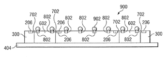
도 8a 및 도 8b는 상기 제조 방법의 제 1 실시예에 따른 몇몇은 유기물질 상에 형성되는 복수의 범프 하의 금속화 층(802)(UMMs)을 성형하는 제 6 단계(800)를 나타내는 도면이다. UBM층은 범프 칩과 패키징 기판을 접속하는 범프와 기판상의 패드 사이에서 구성요소들이 확산하는 것을 막는 차단벽으로서 활성화할 수 있다. 또한, UBM층은 기판상의 패드와 범프 사이의 부착력을 개선한다.8A and 8B illustrate a
또한, UBM층은 솔더에 기반한 범프와 상기 UBM 층 사이에 개량된 칩 접합 특성을 확보하는 습식 층으로서 활성화할 수 있다. 상기와 같은 이점은, A는 예를 들어 금 또는 니켈과 같이 저융점금속(non-refractory metal)이고 B--C는 티타늄/텅스텐(Ti/W)과 같이 쌍을 이루는 합금인, A/B--C의 두개층 구조에 응용되거나, A는 저고융점금속이고 B와 C는 고융점금속인 A/B/C의 세개층 구조에 응용된다.In addition, the UBM layer can be activated as a wet layer to ensure improved chip bonding properties between the solder based bumps and the UBM layer. Such advantages include A / B, where A is a non-refractory metal such as gold or nickel and B--C is a paired alloy such as titanium / tungsten (Ti / W). It is applied to a two-layer structure of --C, or A and a three-layer structure of A / B / C, a low melting point metal and B and C is a high melting point metal.
RDL층(702)의 형성과 같이, UBM(802) 구성요소들의 형성은 다양한 방법론으로 일관하여 수행할 수 있다. UBM(802) 용착은 물리적 증착(예, 스퍼터링(sputtering), 증발), 화학 기상 증착, 또는 다른 유사한 방법들과 같은 여러 방법을 통해 이루어진다. 일례로, UBM(802)는 한가지 금속 또는 적어도 하나의 고융점금속을 포함하는 합금으로 구성된다. 또한, UBM(802)는 단일 고융점금속 또는 합금 층 또는 다수의 층들로 구성될 수 있다. 제조방법의 일례에 있어서, UBM(802)은 수소(H) 열처리 공정에 영향을 받을 수 있다.As with the formation of the
도 9a 및 9b는 상기 제조방법의 제 1 실시예에 따른 상기 범프 하의 금속화 층(802) 상단에 복수의 범프들(902)의 형성을 포함하는 제 7 단계(900)를 나타낸다. 범프들(902)은 여러 기술로 한결같이 형성될 수 있다. 일례로, 범프 전극 들(902)은 포토리소그래피의 전자 부품상에 미리 지정된 레지스트 패턴(resist pattern)을 형성하는 단계를 포함하고, 금속 와이어(wire)에서 금속 볼(ball)을 형성하는 볼(ball) 범프 방법에 의하거나, 솔더, 또는 금(Au) 또는 구리와 같은 금속을 이용하면서 미리 지정된 두께까지 성장되는 레지스트 패턴을 갖는 전해동 도금(electrolytic plating) 방법을 이용하여 형성된다. 또한, 어떤 방법으로라도, 여러 제조방법은 범프들(902)을 제조하는 것으로 이행될 수 있다.9A and 9B illustrate a
도 10a 및 10b 는 상기 제조방법의 제 1 실시예에 따른 제 2 웨이퍼 단일화 단계를 도시하는 제 8 단계(902)를 나타낸다. 웨이퍼 어셈블리(wafer assembly)(300)는 폼 갭(form gap)(904)으로 커팅 소스(402)에 의해 제 2 단계 동안 단일화된다. 상기 방법을 겪는 동안, 도 10a 및 도 10b에 도시된 바와 같은 다양한 다이들(200)과 전술한 예들은 개개의 웨이퍼(300)에서 생산되는 칩 전체의 더 작은 부분(portion)을 나타낸다. 따라서, 후술하는 제 2 단일화 단계의 결과, 다수의 다이들(200)은, 유기물질이 완전히 다이(202)의 둘레 면을 감싸고 범프들(204)이 전술한 바와 같이 다의 각 옆면을 따라 열을 지어 형성되는, 도 2a 및 도 2b 에 도시된 실시예처럼 된다.10A and 10B show an
제 1 실시예에 있어서, 도 10a 및 도 10b에 도시된 후술하는 단일화 단계에서, 개개의 다이들(200)은 다이싱 테이프(404)에서 각 다이(202)를 제거하기 위한 다이 픽 앤 플레이스 공정(die pick and place process)에 의해 제거된다.In the first embodiment, in the singulation step described below in FIGS. 10A and 10B, the individual dies 200 are die pick and place processes for removing each die 202 from the dicing
도 11a 및 도 11b는 도 2a 및 도 2b에서 각각 측면도와 평면도로 도시된 확장된 재배선 층들 범프 웨이퍼 장치(200) 제조방법의 제 2 실시예에 따른 제 3단계 를 나타낸다. 도시된 바와 같이 제 2 실시예는 전술한 제 1 실시예의 상기 첫 번째 두 단계(예, 웨이퍼를 제공하는 단계와 다이싱 테이프(404) 상 각각의 분할물로 단일화하는 단계)가 할당된다. 또한, 다양한 특징(feature)들이 다시 재현된다.11A and 11B show a third step according to a second embodiment of a method of manufacturing the expanded redistribution layers bump
다음 단계로서, 웨이퍼(300) 분할물(500)들은 다이싱 테이프(404)에서 취득되고 도시된 바와 같이 이른바 "웨이퍼 지지 시스템"(wafer support system)(405) 상에 배치된다. 웨이퍼 지지 시스템은 논리적으로 제 2 다이싱 테이프(405)를 포함할 수 있다. 그렇지만, 웨이퍼 지지 시스템은 또한 유리, 세라믹, 라미네이트(laminate), 또는 실리콘(Si) 기판과 같은 일시적인 웨이퍼 지지 시스템이 될 수 있다. 본 발명에서, 톱니형 다이들(202)은 다이싱 테이프(404)에서 취득되고 통상적인 픽 앤 플레이스(pick and place) 기계들을 이용하여 웨이퍼 지지 시스템(405) 상에 배치된다. 픽 앤 플레이스 공정은 각각의 분할물(550)사이에 미리 지정된 폭과 거리(412)를 갖는 갭(gap)(406)이 되게 한다.As a next step,
도 12a 및 도 12b는 도 2a 및 도 2b에 도시된 확장된 재배선 층들 범프 웨이퍼 장치(200)의 제조방법의 제 2 실시예에 따른 제 4단계를 나타낸다. 유기물질(602)은 분할물들(650)에 유사한 스핀 코팅, 니들 디스펜싱, 또는 전술한 다른 방식으로 다시 응용된다. 분할물(650)의 면(642)은 유기물질(602)의 면(654)과 실질적으로 동일 평면이다.12A and 12B show a fourth step according to a second embodiment of a method of manufacturing the expanded redistribution layers bump
다음으로, 도 13a 및 도 13b는 도 2a 및 도 2b에 도시된 장치(200)의 제조방법의 제 2 실시예에 따른 제 5단계를 나타낸다. 리코티드 웨이퍼(recoated wafer)(300)는 제 2 웨이퍼 지지 시스템(408) 상으로 이송된다. 제 2 웨이퍼 지지 시스템은 다시 유리, 실리콘(Si) 기판 재료들, 세라믹, 그리고 라미네이트 재료들을 포함할 수 있다.13A and 13B show a fifth step according to the second embodiment of the manufacturing method of the
도 14a 및 도 14b는 각각 측면도와 평면도인 2a 및 도 2b에 도시된 장치(200)의 제조방법의 제 2 실시예에 따른 제 6단계를 나타낸다. 도 7a 및 도 7b에 도시된 단계와 유사한 단계(750)에 있어서, 재배선 층들(702)은 본드 패드들(206)과 일치하기 위해 유기물질(602) 부분 상단에 형성된다.14A and 14B show a sixth step according to a second embodiment of the method of manufacturing the
도 15a 및 도 15b는 장치(200)의 제조방법의 제 2 실시예에 따른 제 7 단계(850)를 나타낸다. 단계(850)는 UBM(802) 용착 공정인 도 8a 및 도 8b에 도시된 단계와 또한 유사하다.15A and 15B show a
도 16a 및 도 16b는 장치(200)의 제조방법의 제 2 실시예에 따른 제 8 단계(950)를 나타낸다. 일련의 범프들(902)은 도 9a 및 도 9b에 도시된 것과 유사한 공정에서 UBMs(802) 상단에 용착된다.16A and 16B show an
도 17a 및 도 17b는 장치(200)의 제조방법의 제 2 실시예에 따른 제 9 단계(960)를 나타낸다. 도 18a 및 도 18b는 장치들의 제조방법의 제 2 실시예에 따른 일련의 단일화된 다이들(202)을 위해 제 2 단일화 공정인 제 10 단계(970)를 나타낸다. 도 18a 및 도 18b에 도시된 바와 같이, 웨이퍼(300)는 추가 다이싱 테이프(410) 상으로 이송된다. 픽 앤 플레이스 공정은 다음으로 다이싱 테이프(410)에서 복수의 단일화된 다이들(202)을 제거하기 위해 이용된다.17A and 17B show a
범프 웨이퍼 응용을 위한 확장된 재배선 층을 구체화하는 장치(200)와 같은, 반도체 장치들은 여러 응용물에서 다양한 기능(functionality)과 가요 성(flexibility)을 제공할 수 있다. 유기물질(602)의 사용은, 정해진 표면 면적 안에서 추가 입력/출력(I/O) 처리량을 허용하는, 다이(202) 외 측에 범프들(902)의 배치를 가능하게 한다. 또한, 웨이퍼(300) 재료 대신에 유기물질(602)의 사용에 의해, 각각의 웨이퍼마다 산출은 증가 된다. 유기물질(602)은 다수의 실행에서 다양한 다이들을 수용하기에 필요한 만큼 두껍게 형성될 수 있다.Semiconductor devices, such as the
본 발명의 하나의 또는 그 이상의 실시예들이 상세하게 기술되면서, 상기 실시예들의 변형물과 응용물이 본 발명의 범위를 벗어남이 없이 첨부된 특허청구범위의 설명에서 제조되는 것으로 당업자는 해석할 수 있을 것이다.While one or more embodiments of the invention have been described in detail, those skilled in the art can interpret that variations and applications of these embodiments are made in the description of the appended claims without departing from the scope of the invention. There will be.
도 1은 웨이퍼 레벨 칩 스케일 패키지(wafer level chip scale package)의 종래 제조 방법의 예(100)를 나타내는 도면이다.1 is a diagram illustrating an example 100 of a conventional method of manufacturing a wafer level chip scale package.
도 2a는 확장된 재배선층(RDL) 범프 웨이퍼(exteded redistribution layer bumped wafer)의 제 1 실시예를 나타내는 평면도이다.FIG. 2A is a plan view illustrating a first embodiment of an extended redistribution layer bumped wafer. FIG.
도 2b는 도 2a에 도시된 본 발명(200)의 제 1 실시예를 나타내는 측면도이다.FIG. 2B is a side view showing the first embodiment of the
도 2c 는 범프(204)와 본드 패드(206) 사이에 전기적으로 통신 되는 재배선 트레이스들(224)을 병합하는 재배선 층(210)의 부분 확대도이다.2C is an enlarged partial view of the
도 3a 및 도 3b 는 확장된 재배선층 범프 웨이퍼의 제조 방법에 따른 제 1 실시예의 제 1단계를 나타내는 측면도와 평면도이다.3A and 3B are a side view and a plan view showing a first step of the first embodiment according to the method of manufacturing the expanded redistribution layer bump wafer.
도 4a 및 도 4b는 상기 제조 방법의 제 1 실시예에 따른 제 2단계를 나타내는 측면도와 평면도이다.4A and 4B are a side view and a plan view showing a second step according to the first embodiment of the manufacturing method.
도 5a 및 도 5b는 상기 제조 방법의 제 1 실시예에 따른 웨이퍼 분할물들의 확장 방향을 표시하는 제 3단계를 나타낸다.5A and 5B show a third step of indicating the expansion direction of wafer segments according to the first embodiment of the manufacturing method.
도 6a 및 도 6b는 상기 제조 방법의 제 1 실시예에 따른 복수의 간격들에 유기물질의 증착하는 제 4단계를 나타낸다.6A and 6B illustrate a fourth step of depositing an organic material at a plurality of intervals according to the first embodiment of the manufacturing method.
도 7a 및 도 7b는 상기 제조 방법의 제 1 실시예에 따른 재배선 층들(702)에서 패턴화되는 제 5 단계(700)를 나타낸다.7A and 7B show a
도 8a 및 도 8b는 상기 제조 방법의 제 1 실시예에 따른 몇몇은 유기물질 상 에 형성되는 복수의 범프 하의 금속화 층(802)(UMMs)을 성형하는 제 6 단계(800)를 나타내는 도면이다.8A and 8B show a
도 9a 및 9b는 상기 제조방법의 제 1 실시예에 따른 상기 범프 하의 금속화 층(802) 상단에 복수의 범프들(902)의 형성을 포함하는 제 7 단계(900)를 나타낸다.9A and 9B illustrate a
도 10a 및 10b 는 상기 제조방법의 제 1 실시예에 따른 제 2 웨이퍼 단일화 단계를 도시하는 제 8 단계(902)를 나타낸다.10A and 10B show an
도 11a 및 도 11b는 도 2a 및 도 2b에서 각각 측면도와 평면도로 도시된 확장된 재배선 층들 범프 웨이퍼 장치(200) 제조방법의 제 2 실시예에 따른 제 3단계를 나타낸다.11A and 11B show a third step according to a second embodiment of a method of manufacturing the expanded redistribution layers bump
도 12a 및 도 12b는 도 2a 및 도 2b에 도시된 확장된 재배선 층들 범프 웨이퍼 장치(200)의 제조방법의 제 2 실시예에 따른 제 4단계를 나타낸다.12A and 12B show a fourth step according to a second embodiment of a method of manufacturing the expanded redistribution layers bump
도 13a 및 도 13b는 도 2a 및 도 2b에 도시된 장치(200)의 제조방법의 제 2 실시예에 따른 제 5단계를 나타낸다.13A and 13B show a fifth step according to the second embodiment of the method of manufacturing the
도 14a 및 도 14b는 각각 측면도와 평면도인 2a 및 도 2b에 도시된 장치(200)의 제조방법의 제 2 실시예에 따른 제 6단계를 나타낸다.14A and 14B show a sixth step according to a second embodiment of the method of manufacturing the
도 15a 및 도 15b는 장치(200)의 제조방법의 제 2 실시예에 따른 제 7 단계(850)를 나타낸다.15A and 15B show a
도 16a 및 도 16b는 장치(200)의 제조방법의 제 2 실시예에 따른 제 8 단계(950)를 나타낸다.16A and 16B show an
도 17a 및 도 17b는 장치(200)의 제조방법의 제 2 실시예에 따른 제 9 단계(960)를 나타낸다.17A and 17B show a
도 18a 및 도 18b는 장치들의 제조방법의 제 2 실시예에 따른 일련의 단일화된 다이들(202)을 위해 제 2 단일화 공정인 제 10 단계(970)를 나타낸다.18A and 18B show a
Claims (27)
Applications Claiming Priority (2)
| Application Number | Priority Date | Filing Date | Title |
|---|---|---|---|
| US11/744,743 | 2007-05-04 | ||
| US11/744,743 US7687318B2 (en) | 2007-05-04 | 2007-05-04 | Extended redistribution layers bumped wafer |
Publications (2)
| Publication Number | Publication Date |
|---|---|
| KR20080098335A true KR20080098335A (en) | 2008-11-07 |
| KR101497697B1 KR101497697B1 (en) | 2015-03-02 |
Family
ID=39938940
Family Applications (1)
| Application Number | Title | Priority Date | Filing Date |
|---|---|---|---|
| KR1020080042039A Active KR101497697B1 (en) | 2007-05-04 | 2008-05-06 | Semiconductor device and manufacturing method thereof |
Country Status (4)
| Country | Link |
|---|---|
| US (3) | US7687318B2 (en) |
| KR (1) | KR101497697B1 (en) |
| SG (3) | SG162789A1 (en) |
| TW (1) | TWI425583B (en) |
Families Citing this family (27)
| Publication number | Priority date | Publication date | Assignee | Title |
|---|---|---|---|---|
| US7723159B2 (en) * | 2007-05-04 | 2010-05-25 | Stats Chippac, Ltd. | Package-on-package using through-hole via die on saw streets |
| US8445325B2 (en) | 2007-05-04 | 2013-05-21 | Stats Chippac, Ltd. | Package-in-package using through-hole via die on saw streets |
| US7829998B2 (en) | 2007-05-04 | 2010-11-09 | Stats Chippac, Ltd. | Semiconductor wafer having through-hole vias on saw streets with backside redistribution layer |
| TWI387014B (en) * | 2008-06-05 | 2013-02-21 | 南茂科技股份有限公司 | Die reconfiguration structure with sacrificial substrate and packaging method thereof |
| US8021907B2 (en) | 2008-06-09 | 2011-09-20 | Stats Chippac, Ltd. | Method and apparatus for thermally enhanced semiconductor package |
| US8298917B2 (en) * | 2009-04-14 | 2012-10-30 | International Business Machines Corporation | Process for wet singulation using a dicing singulation structure |
| US8420554B2 (en) * | 2010-05-03 | 2013-04-16 | Memc Electronic Materials, Inc. | Wafer support ring |
| JP5594661B2 (en) * | 2010-06-15 | 2014-09-24 | ルネサスエレクトロニクス株式会社 | Semiconductor device |
| JP5539077B2 (en) | 2010-07-09 | 2014-07-02 | ローム株式会社 | Semiconductor device |
| US9324659B2 (en) * | 2011-08-01 | 2016-04-26 | Stats Chippac, Ltd. | Semiconductor device and method of forming POP with stacked semiconductor die and bumps formed directly on the lower die |
| US8617927B1 (en) * | 2011-11-29 | 2013-12-31 | Hrl Laboratories, Llc | Method of mounting electronic chips |
| KR101411813B1 (en) * | 2012-11-09 | 2014-06-27 | 앰코 테크놀로지 코리아 주식회사 | Semiconductor device and manufacturing method thereof |
| US10079160B1 (en) | 2013-06-21 | 2018-09-18 | Hrl Laboratories, Llc | Surface mount package for semiconductor devices with embedded heat spreaders |
| TWI566339B (en) * | 2014-11-11 | 2017-01-11 | 矽品精密工業股份有限公司 | Electronic package and its manufacturing method |
| US10515939B2 (en) | 2015-02-17 | 2019-12-24 | Mediatek Inc. | Wafer-level package having multiple dies arranged in side-by-side fashion and associated yield improvement method |
| US10037293B2 (en) | 2015-02-17 | 2018-07-31 | Nephos (Hefei) Co. Ltd. | Wafer-level package having asynchronous FIFO buffer used to deal with data transfer between different dies and associated method |
| US9385083B1 (en) | 2015-05-22 | 2016-07-05 | Hrl Laboratories, Llc | Wafer-level die to package and die to die interconnects suspended over integrated heat sinks |
| US10026672B1 (en) | 2015-10-21 | 2018-07-17 | Hrl Laboratories, Llc | Recursive metal embedded chip assembly |
| US9508652B1 (en) | 2015-11-24 | 2016-11-29 | Hrl Laboratories, Llc | Direct IC-to-package wafer level packaging with integrated thermal heat spreaders |
| US9698108B1 (en) | 2015-12-23 | 2017-07-04 | Intel Corporation | Structures to mitigate contamination on a back side of a semiconductor substrate |
| US9985040B2 (en) | 2016-01-14 | 2018-05-29 | Micron Technology, Inc. | Integrated circuitry and 3D memory |
| US10483239B2 (en) * | 2016-12-20 | 2019-11-19 | Sandisk Semiconductor (Shanghai) Co. Ltd. | Semiconductor device including dual pad wire bond interconnection |
| US10566268B1 (en) * | 2018-09-26 | 2020-02-18 | Nxp Usa, Inc. | Package to die connection system and method therefor |
| US10950562B1 (en) | 2018-11-30 | 2021-03-16 | Hrl Laboratories, Llc | Impedance-matched through-wafer transition using integrated heat-spreader technology |
| US12604733B2 (en) * | 2022-03-31 | 2026-04-14 | Intel Corporation | Package structures with collapse control features |
| US12604754B2 (en) | 2022-03-31 | 2026-04-14 | Intel Corporation | Package structures with non-uniform interconnect features |
| US12598989B2 (en) | 2022-03-31 | 2026-04-07 | Intel Corporation | Package structures with patterned die backside layer |
Family Cites Families (20)
| Publication number | Priority date | Publication date | Assignee | Title |
|---|---|---|---|---|
| EP0011418A1 (en) * | 1978-11-20 | 1980-05-28 | THE GENERAL ELECTRIC COMPANY, p.l.c. | Manufacture of electroluminescent display devices |
| JPH01280340A (en) * | 1988-05-06 | 1989-11-10 | Nec Corp | Manufacture of semiconductor device |
| US6511901B1 (en) * | 1999-11-05 | 2003-01-28 | Atmel Corporation | Metal redistribution layer having solderable pads and wire bondable pads |
| TW451436B (en) * | 2000-02-21 | 2001-08-21 | Advanced Semiconductor Eng | Manufacturing method for wafer-scale semiconductor packaging structure |
| TW502344B (en) * | 2000-12-07 | 2002-09-11 | Advanced Semiconductor Eng | Chip scale package structure and its manufacturing method |
| JP3848080B2 (en) * | 2000-12-19 | 2006-11-22 | 富士通株式会社 | Manufacturing method of semiconductor device |
| KR20020091327A (en) * | 2001-05-31 | 2002-12-06 | 삼성전자 주식회사 | Wafer level package having a package body at its side surface and method for manufacturing the same |
| US6787895B1 (en) * | 2001-12-07 | 2004-09-07 | Skyworks Solutions, Inc. | Leadless chip carrier for reduced thermal resistance |
| TW544882B (en) * | 2001-12-31 | 2003-08-01 | Megic Corp | Chip package structure and process thereof |
| US7208344B2 (en) * | 2004-03-31 | 2007-04-24 | Aptos Corporation | Wafer level mounting frame for ball grid array packaging, and method of making and using the same |
| US20050227382A1 (en) * | 2004-04-02 | 2005-10-13 | Hui Angela T | In-situ surface treatment for memory cell formation |
| JP2005322858A (en) | 2004-05-11 | 2005-11-17 | Shinko Electric Ind Co Ltd | Manufacturing method of semiconductor device |
| KR20060115095A (en) * | 2005-05-04 | 2006-11-08 | 삼성전기주식회사 | Surface acoustic wave device package with excellent airtightness |
| US7208345B2 (en) * | 2005-05-11 | 2007-04-24 | Infineon Technologies Ag | Method of manufacturing a semiconductor device comprising stacked chips and a corresponding semiconductor device |
| US7728437B2 (en) * | 2005-11-23 | 2010-06-01 | Fairchild Korea Semiconductor, Ltd. | Semiconductor package form within an encapsulation |
| US7750452B2 (en) * | 2007-05-04 | 2010-07-06 | Stats Chippac, Ltd. | Same size die stacked package having through-hole vias formed in organic material |
| US8390107B2 (en) * | 2007-09-28 | 2013-03-05 | Intel Mobile Communications GmbH | Semiconductor device and methods of manufacturing semiconductor devices |
| SG152086A1 (en) * | 2007-10-23 | 2009-05-29 | Micron Technology Inc | Packaged semiconductor assemblies and associated systems and methods |
| US8030136B2 (en) * | 2008-05-15 | 2011-10-04 | Stats Chippac, Ltd. | Semiconductor device and method of conforming conductive vias between insulating layers in saw streets |
| US8093151B2 (en) * | 2009-03-13 | 2012-01-10 | Stats Chippac, Ltd. | Semiconductor die and method of forming noise absorbing regions between THVS in peripheral region of the die |
-
2007
- 2007-05-04 US US11/744,743 patent/US7687318B2/en active Active
-
2008
- 2008-04-02 TW TW097111945A patent/TWI425583B/en active
- 2008-04-14 SG SG201004169-7A patent/SG162789A1/en unknown
- 2008-04-14 SG SG2013070099A patent/SG194354A1/en unknown
- 2008-04-14 SG SG200802844-1A patent/SG147384A1/en unknown
- 2008-05-06 KR KR1020080042039A patent/KR101497697B1/en active Active
-
2010
- 2010-02-11 US US12/704,345 patent/US8716853B2/en active Active
-
2014
- 2014-03-14 US US14/214,120 patent/US9406647B2/en active Active
Also Published As
| Publication number | Publication date |
|---|---|
| SG194354A1 (en) | 2013-11-29 |
| US20100140799A1 (en) | 2010-06-10 |
| US20080272368A1 (en) | 2008-11-06 |
| SG147384A1 (en) | 2008-11-28 |
| KR101497697B1 (en) | 2015-03-02 |
| US8716853B2 (en) | 2014-05-06 |
| US9406647B2 (en) | 2016-08-02 |
| TWI425583B (en) | 2014-02-01 |
| US20140197540A1 (en) | 2014-07-17 |
| US7687318B2 (en) | 2010-03-30 |
| TW200903677A (en) | 2009-01-16 |
| SG162789A1 (en) | 2010-07-29 |
Similar Documents
| Publication | Publication Date | Title |
|---|---|---|
| KR101497697B1 (en) | Semiconductor device and manufacturing method thereof | |
| US11508635B2 (en) | Semiconductor package having routable encapsulated conductive substrate and method | |
| KR102597994B1 (en) | Connection structure and method of forming the same | |
| US7843052B1 (en) | Semiconductor devices and fabrication methods thereof | |
| CN102543923B (en) | Semiconductor device and manufacture method thereof | |
| KR102067840B1 (en) | A semiconductor device and a method of making a semiconductor device | |
| TWI427754B (en) | a package in a package using via die on a saw blade | |
| KR101523383B1 (en) | Semiconductor device and manufacturing method thereof | |
| CN109904127B (en) | Packaging structure and packaging method | |
| KR101514137B1 (en) | Method for fabricating semiconductor package and semiconductor package using the same | |
| US20180130769A1 (en) | Substrate Based Fan-Out Wafer Level Packaging | |
| CN104733379A (en) | Semiconductor device and method of forming fine pitch rdl over semiconductor die in fan-out package | |
| KR101235498B1 (en) | Methods and systems for packaging integrated circuits with integrated passive components | |
| KR101571604B1 (en) | Single mask package apparatus and method | |
| KR101758999B1 (en) | Semiconductor device and manufacturing method thereof | |
| CN104425419A (en) | Semiconductor device and manufacturing method thereof | |
| US20240203919A1 (en) | Integrated circuit having exposed leads | |
| US20180130720A1 (en) | Substrate Based Fan-Out Wafer Level Packaging | |
| CN121035063A (en) | Electronic devices and methods for manufacturing electronic devices | |
| KR20170036235A (en) | Wafer level fan out package and method for manufacturing the same | |
| KR20170036238A (en) | Laminated wafer level fan out package and method for manufacturing the same |
Legal Events
| Date | Code | Title | Description |
|---|---|---|---|
| PA0109 | Patent application |
St.27 status event code: A-0-1-A10-A12-nap-PA0109 |
|
| PG1501 | Laying open of application |
St.27 status event code: A-1-1-Q10-Q12-nap-PG1501 |
|
| A201 | Request for examination | ||
| E13-X000 | Pre-grant limitation requested |
St.27 status event code: A-2-3-E10-E13-lim-X000 |
|
| P11-X000 | Amendment of application requested |
St.27 status event code: A-2-2-P10-P11-nap-X000 |
|
| P13-X000 | Application amended |
St.27 status event code: A-2-2-P10-P13-nap-X000 |
|
| PA0201 | Request for examination |
St.27 status event code: A-1-2-D10-D11-exm-PA0201 |
|
| E902 | Notification of reason for refusal | ||
| PE0902 | Notice of grounds for rejection |
St.27 status event code: A-1-2-D10-D21-exm-PE0902 |
|
| T11-X000 | Administrative time limit extension requested |
St.27 status event code: U-3-3-T10-T11-oth-X000 |
|
| R17-X000 | Change to representative recorded |
St.27 status event code: A-3-3-R10-R17-oth-X000 |
|
| P11-X000 | Amendment of application requested |
St.27 status event code: A-2-2-P10-P11-nap-X000 |
|
| P13-X000 | Application amended |
St.27 status event code: A-2-2-P10-P13-nap-X000 |
|
| R17-X000 | Change to representative recorded |
St.27 status event code: A-3-3-R10-R17-oth-X000 |
|
| E701 | Decision to grant or registration of patent right | ||
| PE0701 | Decision of registration |
St.27 status event code: A-1-2-D10-D22-exm-PE0701 |
|
| GRNT | Written decision to grant | ||
| PR0701 | Registration of establishment |
St.27 status event code: A-2-4-F10-F11-exm-PR0701 |
|
| PR1002 | Payment of registration fee |
St.27 status event code: A-2-2-U10-U11-oth-PR1002 Fee payment year number: 1 |
|
| PG1601 | Publication of registration |
St.27 status event code: A-4-4-Q10-Q13-nap-PG1601 |
|
| R18-X000 | Changes to party contact information recorded |
St.27 status event code: A-5-5-R10-R18-oth-X000 |
|
| S20-X000 | Security interest recorded |
St.27 status event code: A-4-4-S10-S20-lic-X000 |
|
| FPAY | Annual fee payment |
Payment date: 20180208 Year of fee payment: 4 |
|
| PR1001 | Payment of annual fee |
St.27 status event code: A-4-4-U10-U11-oth-PR1001 Fee payment year number: 4 |
|
| FPAY | Annual fee payment |
Payment date: 20190212 Year of fee payment: 5 |
|
| PR1001 | Payment of annual fee |
St.27 status event code: A-4-4-U10-U11-oth-PR1001 Fee payment year number: 5 |
|
| S22-X000 | Recordation of security interest cancelled |
St.27 status event code: A-4-4-S10-S22-lic-X000 |
|
| R18-X000 | Changes to party contact information recorded |
St.27 status event code: A-5-5-R10-R18-oth-X000 |
|
| FPAY | Annual fee payment |
Payment date: 20200214 Year of fee payment: 6 |
|
| PR1001 | Payment of annual fee |
St.27 status event code: A-4-4-U10-U11-oth-PR1001 Fee payment year number: 6 |
|
| PR1001 | Payment of annual fee |
St.27 status event code: A-4-4-U10-U11-oth-PR1001 Fee payment year number: 7 |
|
| PR1001 | Payment of annual fee |
St.27 status event code: A-4-4-U10-U11-oth-PR1001 Fee payment year number: 8 |
|
| PR1001 | Payment of annual fee |
St.27 status event code: A-4-4-U10-U11-oth-PR1001 Fee payment year number: 9 |
|
| PR1001 | Payment of annual fee |
St.27 status event code: A-4-4-U10-U11-oth-PR1001 Fee payment year number: 10 |
|
| PR1001 | Payment of annual fee |
St.27 status event code: A-4-4-U10-U11-oth-PR1001 Fee payment year number: 11 |
|
| PN2301 | Change of applicant |
St.27 status event code: A-5-5-R10-R13-asn-PN2301 St.27 status event code: A-5-5-R10-R11-asn-PN2301 |
|
| P22-X000 | Classification modified |
St.27 status event code: A-4-4-P10-P22-nap-X000 |