US10026672B1 - Recursive metal embedded chip assembly - Google Patents
Recursive metal embedded chip assembly Download PDFInfo
- Publication number
- US10026672B1 US10026672B1 US15/299,348 US201615299348A US10026672B1 US 10026672 B1 US10026672 B1 US 10026672B1 US 201615299348 A US201615299348 A US 201615299348A US 10026672 B1 US10026672 B1 US 10026672B1
- Authority
- US
- United States
- Prior art keywords
- carrier
- integrated circuit
- packaging
- circuit chips
- thermally conductive
- Prior art date
- Legal status (The legal status is an assumption and is not a legal conclusion. Google has not performed a legal analysis and makes no representation as to the accuracy of the status listed.)
- Active
Links
Images


Classifications
-
- H—ELECTRICITY
- H01—ELECTRIC ELEMENTS
- H01L—SEMICONDUCTOR DEVICES NOT COVERED BY CLASS H10
- H01L23/00—Details of semiconductor or other solid state devices
- H01L23/34—Arrangements for cooling, heating, ventilating or temperature compensation ; Temperature sensing arrangements
- H01L23/36—Selection of materials, or shaping, to facilitate cooling or heating, e.g. heatsinks
- H01L23/373—Cooling facilitated by selection of materials for the device or materials for thermal expansion adaptation, e.g. carbon
- H01L23/3736—Metallic materials
-
- H—ELECTRICITY
- H01—ELECTRIC ELEMENTS
- H01L—SEMICONDUCTOR DEVICES NOT COVERED BY CLASS H10
- H01L21/00—Processes or apparatus adapted for the manufacture or treatment of semiconductor or solid state devices or of parts thereof
- H01L21/02—Manufacture or treatment of semiconductor devices or of parts thereof
- H01L21/04—Manufacture or treatment of semiconductor devices or of parts thereof the devices having at least one potential-jump barrier or surface barrier, e.g. PN junction, depletion layer or carrier concentration layer
- H01L21/48—Manufacture or treatment of parts, e.g. containers, prior to assembly of the devices, using processes not provided for in a single one of the subgroups H01L21/06 - H01L21/326
- H01L21/4814—Conductive parts
- H01L21/4871—Bases, plates or heatsinks
- H01L21/4882—Assembly of heatsink parts
-
- H—ELECTRICITY
- H01—ELECTRIC ELEMENTS
- H01L—SEMICONDUCTOR DEVICES NOT COVERED BY CLASS H10
- H01L21/00—Processes or apparatus adapted for the manufacture or treatment of semiconductor or solid state devices or of parts thereof
- H01L21/02—Manufacture or treatment of semiconductor devices or of parts thereof
- H01L21/04—Manufacture or treatment of semiconductor devices or of parts thereof the devices having at least one potential-jump barrier or surface barrier, e.g. PN junction, depletion layer or carrier concentration layer
- H01L21/50—Assembly of semiconductor devices using processes or apparatus not provided for in a single one of the subgroups H01L21/06 - H01L21/326, e.g. sealing of a cap to a base of a container
- H01L21/56—Encapsulations, e.g. encapsulation layers, coatings
- H01L21/568—Temporary substrate used as encapsulation process aid
-
- H—ELECTRICITY
- H01—ELECTRIC ELEMENTS
- H01L—SEMICONDUCTOR DEVICES NOT COVERED BY CLASS H10
- H01L23/00—Details of semiconductor or other solid state devices
- H01L23/28—Encapsulations, e.g. encapsulating layers, coatings, e.g. for protection
- H01L23/31—Encapsulations, e.g. encapsulating layers, coatings, e.g. for protection characterised by the arrangement or shape
- H01L23/3107—Encapsulations, e.g. encapsulating layers, coatings, e.g. for protection characterised by the arrangement or shape the device being completely enclosed
-
- H—ELECTRICITY
- H01—ELECTRIC ELEMENTS
- H01L—SEMICONDUCTOR DEVICES NOT COVERED BY CLASS H10
- H01L23/00—Details of semiconductor or other solid state devices
- H01L23/34—Arrangements for cooling, heating, ventilating or temperature compensation ; Temperature sensing arrangements
- H01L23/36—Selection of materials, or shaping, to facilitate cooling or heating, e.g. heatsinks
- H01L23/367—Cooling facilitated by shape of device
- H01L23/3675—Cooling facilitated by shape of device characterised by the shape of the housing
-
- H—ELECTRICITY
- H01—ELECTRIC ELEMENTS
- H01L—SEMICONDUCTOR DEVICES NOT COVERED BY CLASS H10
- H01L24/00—Arrangements for connecting or disconnecting semiconductor or solid-state bodies; Methods or apparatus related thereto
- H01L24/93—Batch processes
- H01L24/95—Batch processes at chip-level, i.e. with connecting carried out on a plurality of singulated devices, i.e. on diced chips
- H01L24/96—Batch processes at chip-level, i.e. with connecting carried out on a plurality of singulated devices, i.e. on diced chips the devices being encapsulated in a common layer, e.g. neo-wafer or pseudo-wafer, said common layer being separable into individual assemblies after connecting
-
- H—ELECTRICITY
- H01—ELECTRIC ELEMENTS
- H01L—SEMICONDUCTOR DEVICES NOT COVERED BY CLASS H10
- H01L21/00—Processes or apparatus adapted for the manufacture or treatment of semiconductor or solid state devices or of parts thereof
- H01L21/02—Manufacture or treatment of semiconductor devices or of parts thereof
- H01L21/04—Manufacture or treatment of semiconductor devices or of parts thereof the devices having at least one potential-jump barrier or surface barrier, e.g. PN junction, depletion layer or carrier concentration layer
- H01L21/50—Assembly of semiconductor devices using processes or apparatus not provided for in a single one of the subgroups H01L21/06 - H01L21/326, e.g. sealing of a cap to a base of a container
- H01L21/56—Encapsulations, e.g. encapsulation layers, coatings
- H01L21/561—Batch processing
-
- H—ELECTRICITY
- H01—ELECTRIC ELEMENTS
- H01L—SEMICONDUCTOR DEVICES NOT COVERED BY CLASS H10
- H01L2224/00—Indexing scheme for arrangements for connecting or disconnecting semiconductor or solid-state bodies and methods related thereto as covered by H01L24/00
- H01L2224/01—Means for bonding being attached to, or being formed on, the surface to be connected, e.g. chip-to-package, die-attach, "first-level" interconnects; Manufacturing methods related thereto
- H01L2224/18—High density interconnect [HDI] connectors; Manufacturing methods related thereto
- H01L2224/23—Structure, shape, material or disposition of the high density interconnect connectors after the connecting process
- H01L2224/24—Structure, shape, material or disposition of the high density interconnect connectors after the connecting process of an individual high density interconnect connector
- H01L2224/241—Disposition
- H01L2224/24135—Connecting between different semiconductor or solid-state bodies, i.e. chip-to-chip
- H01L2224/24137—Connecting between different semiconductor or solid-state bodies, i.e. chip-to-chip the bodies being arranged next to each other, e.g. on a common substrate
-
- H—ELECTRICITY
- H01—ELECTRIC ELEMENTS
- H01L—SEMICONDUCTOR DEVICES NOT COVERED BY CLASS H10
- H01L2224/00—Indexing scheme for arrangements for connecting or disconnecting semiconductor or solid-state bodies and methods related thereto as covered by H01L24/00
- H01L2224/01—Means for bonding being attached to, or being formed on, the surface to be connected, e.g. chip-to-package, die-attach, "first-level" interconnects; Manufacturing methods related thereto
- H01L2224/18—High density interconnect [HDI] connectors; Manufacturing methods related thereto
- H01L2224/23—Structure, shape, material or disposition of the high density interconnect connectors after the connecting process
- H01L2224/24—Structure, shape, material or disposition of the high density interconnect connectors after the connecting process of an individual high density interconnect connector
- H01L2224/241—Disposition
- H01L2224/24151—Connecting between a semiconductor or solid-state body and an item not being a semiconductor or solid-state body, e.g. chip-to-substrate, chip-to-passive
- H01L2224/24153—Connecting between a semiconductor or solid-state body and an item not being a semiconductor or solid-state body, e.g. chip-to-substrate, chip-to-passive the body and the item being arranged next to each other, e.g. on a common substrate
- H01L2224/24195—Connecting between a semiconductor or solid-state body and an item not being a semiconductor or solid-state body, e.g. chip-to-substrate, chip-to-passive the body and the item being arranged next to each other, e.g. on a common substrate the item being a discrete passive component
Definitions
- the present disclosure is directed in general to wafer level packaging of integrated circuits and in particular to multi-scale and multi-chip integration.
- wire bonds have been used in the prior art for both connecting contacts on a chip to its package and also for chip to chip connections when multiple chips reside in a single package.
- the wire bonds now are so large compared with the device geometries of modern integrated chips (ICs) that their size can make it difficult to couple modern ICs either with pins in the packaging in which the ICs reside or with neighboring ICs when multiple ICs are packaged together.
- U.S. Pat. No. 8,617,927 which is incorporated herein, teaches a method of mounting electronic dies or chips into an electroformed heat spreader offering an integrated solution to thermal management at the single-level wafer-scale integration.
- U.S. application Ser. No. 15/169,591, incorporated herein addresses another important technology in connecting die to package using electroplated and suspended interconnects over integrated heat spreaders.
- U.S. application Ser. No. 14/950,667 (141211) which is also incorporated herein, addresses another aspect of the single-level wafer-scale integration of direct IC-to-package wafer-level packaging with integrated thermal heat spreaders.
- R-MECA recursive metal-embedded chip assembly
- component modules each comprise at least one of an assembly prepared using the metal embedded chip assembly (MECA) process, an Integrated Circuit (IC) chip, a macro cell, and a die, embedding a heat spreader material on the assembly, releasing the carrier substrate from the two or more component modules and forming interconnects between the component modules, by forming multilayer interconnects on the side where the carrier substrate was released.
- MECA metal embedded chip assembly
- IC Integrated Circuit
- the disclosure covers the product made by the process comprising, dicing of one or more metal embedded chip assembly (MECA) modules, assembling the MECA modules on a carrier substrate with face-down, attaching a packaging substrate, embedding metal by filling the holes in the packaging substrate, releasing the substrate, flipping the wafer and forming interconnects, wherein MECA modules comprise of assemblies prepared using the metal embedded chip assembly process and/or any Integrated Circuit (IC) chips and/or any macro cell and/or a die fabricated in any technology.
- MECA metal embedded chip assembly
- the disclosure also provides for a process of integrating discrete components to the MECA modules and recursively using the process described above to achieve a large scale integration with integrated thermal spreaders.
- Certain embodiments may provide various technical features depending on the implementation.
- a technical feature of some embodiments may include the capability to provide for large scale integration of different technology dies.
- FIG. 1 illustrates a process flow of metal embedded chip assembly (MECA);
- FIGS. 2, 3 and 4 illustrate detailed steps of the process flow in FIG. 1 ;
- FIG. 5 illustrates a process flow of recursive metal embedded chip assembly (R-MECA), according to an embodiment of the present disclosure
- FIGS. 6, 7 and 8 illustrate detailed steps of recursive metal embedded chip assembly (R-MECA) of FIG. 5 , according to an embodiment of the present disclosure
- FIG. 9A illustrates multi-chip (COTS) integration in copper electroformed heat spreader with front side interconnects
- FIG. 9B illustrates module integration with second embedded heat spreader board-to-MECA_0 interconnects as part of a module integration process flow, according to an embodiment of the present disclosure
- FIG. 10A illustrates integration of discrete components to the assembled module of FIG. 9B , according to an embodiment of the present disclosure
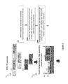
- FIG. 10B illustrates a scaled rendering of MECA-integrated Ku-band power amplifier module demonstrating IP re-use through heterogeneous COTS integration according to an embodiment of the present disclosure
- FIG. 11 illustrates multi-scale integration of dies, chips and IP blocks into a single packaged module with integrated heat spreader, according to an embodiment of the present disclosure.
- the proposed technology presents a recursive metal-embedded chip assembly (R-MECA) technology for heterogeneous integration of multiple die from diverse device technologies.
- R-MECA recursive metal-embedded chip assembly
- One of the features of this disclosure is the “recursive” aspect of this integration technology, which enables integration of increasingly-complex subsystems while bridging different scales for devices, interconnects and components. Additionally, high thermal management performance is maintained through the multiple recursive levels of R-MECA, a key requirement for high-performance heterogeneous integration of digital, analog mixed signal and RF subsystems.
- wire bonding techniques are used when it comes to interconnecting heterogeneous devices.
- This disclosure introduces a new technology which effectively replaces prior art wire bonding techniques with a new die to package and die to die interconnects which may be conveniently suspended over electrically conductive surfaces such as integrated heat sinks (or heat spreaders) which may be included in the packaging.
- the new technology is particularly suitable for wafer-level integration and wafer-level processing, which enables parallel interconnection of a multitude of chips at the wafer scale.
- chips from diverse technologies and different thicknesses are initially embedded in a metal heat spreader surrounded by a mesh wafer serving as a host.
- the approach uses metal embedding on the backside of the chips as a key differentiator to achieve among other things, high-density integration and built-in thermal management.
- wafer-level front side interconnects are fabricated to interconnect the various chips with each other.
- the wafer is then diced into individual MECA modules, and forms the level one for multi-scale R-MECA integration. These modules are subsequently integrated into another wafer or board using the same integration approach recursively. Additional components such as discrete passive resistors, capacitors, inductors can be integrated at the second level, once the high-resolution, high-density integration has been performed at the level zero.
- MECA Metal Embedded Chip Assembly
- the standard MECA integration process flow 100 is illustrated in FIG. 1 .
- this MECA process flow comprises of preparing various IC chips or IP blocks that make up an integrated chip or a module ( 110 ), followed by assembling these blocks on a substrate to form an integrated chip assembly ( 120 ), followed by a metal embedding process ( 130 ) and subsequently releasing the substrate and flipping the wafer ( 140 ).
- the final step 150 comprises of exposing the pads for forming the interconnects between the various blocks.
- FIGS. 2, 3 and 4 describe this MECA process steps in detail.
- the first step 110 in the MECA process is to dice the IC chips or the IP blocks or macros that need to be put together and interconnected in the MECA process. They can be from one or more different technologies or from the same technology family. In the illustration of FIG. 2, 111 represent a die from an IC chip, while 112 is another die from a different technology and 113 is an IP Macro. They are first diced in step 110 .
- Next step 120 comprises of several sub-steps 120 A and 120 B.
- step 120 IC chips and a mesh wafer (packaging form) are only temporarily bonded face down on a carrier wafer coated with adhesive.
- step 120 A the dies of chips and macros are mounted on a carrier substrate face down and temporarily bonded using a die bonder 123 .
- a pre-fabricated packaging form 122 with pre-fabricated through-substrate holes is installed, aligned and temporarily bonded onto the carrier substrate 121 .
- This chip assembly on the substrate can take place at room temperature with a die bonder.
- the packaging form can be made from a substrate or other suitable material.
- FIG. 3 illustrates the next two steps, 130 and 140 .
- a high-thermal conductivity (e.g., copper) heat spreader is electroformed on the backside of the chips, enabling high-density chip integration as well as high-performance thermal management due to the intimate contact between the heat spreader and the chips.
- Step 130 comprises of three sub-steps.
- a layer of metal, such as copper is sputtered on the assembly from the step 120 B.
- the holes in the packaging substrate are filled with a metal such as copper.
- the sputtering of metal in the step 130 A is used as a seed layer and then the material of choice is electroformed on top of this seed layer.
- Planarization takes place after electroforming, to remove any protruding metal.
- step 140 A involves releasing the substrate 121 from the temporary carrier by any known means, followed by flipping the substrate (step 140 B) to get the IC Chips and macros face up and embedded in the metal heat sink 131 .
- FIG. 4 describes the last step in the MECA process.
- This step 150 comprises of chip delayering to expose the pads for interconnect and to form the interconnects.
- Step 150 A comprises of any front side processing needed to perform multi-layer interconnects and may use standard IC process technologies and standard micro fabrication technologies to realize high-resolution front side chip-to-chip and chip-to-package interconnects.
- the final step 150 B involves dicing the individual MECA modules as desired.
- each of the component modules comprise at least one of an assembly prepared using the metal embedded chip assembly (MECA) process, an Integrated Circuit (IC) chip, a macro cell, and a die.
- MECA metal embedded chip assembly
- IC Integrated Circuit
- the modules which feature different IP blocks, and typically different die and interconnect scales, are then integrated using the recursive MECA approach, which is a structured repeat of the process shown in FIG. 1 .
- This recursive MECA (R-MECA) process 500 illustrated in FIG. 5 comprises of five major steps.
- the first step 510 starts off with two or more MECA modules prepared in the process 100 described earlier.
- This step 510 is followed by assembling these MESA modules on a substrate to form an integrated module assembly ( 520 ), followed by a metal embedding process ( 530 ) and subsequently releasing the substrate and flipping the wafer ( 540 ).
- the final step 550 comprises of exposing the pads of these integrated MECA modules for forming the interconnects between the various modules.
- FIGS. 6, 7 and 8 describe this R-MECA process steps in detail. It must be noted that the process 500 not only can integrate several MECA modules, it can also integrate IC chips and IP macros with one or more MECA modules.
- the first step 510 in the R-MECA process is to dice and sort out the MECA modules and/or IC chips or the IP blocks or macros of similar or dissimilar technologies that need to be put together and interconnected in the MECA process.
- 511 represent a die from a MECA module 1
- 512 is another die from a different technology MECA module. They are first diced in step 510 .
- Next step 520 comprises of several sub-steps 520 A and 520 B.
- MECA modules and other IC chips or macros and a mesh wafer (packaging substrate) are only temporarily bonded face down on a carrier wafer coated with adhesive.
- step 520 A the dies of modules and chips are mounted and aligned to micron level resolution on a carrier substrate face down and temporarily bonded using a die bonder 523 .
- step 520 B a pre-fabricated packaging substrate 522 with pre-fabricated through-substrate holes is installed, aligned and temporarily bonded onto the carrier substrate 521 .
- This R-MECA assembly on the substrate can take place at room temperature with a die bonder.
- FIG. 7 illustrates the next two steps, 530 and 540 .
- a high-thermal conductivity (e.g., copper) heat spreader is electroformed on the backside of the assembly, enabling high-density chip integration as well as high-performance thermal management due to the intimate contact between the heat spreader and the assembled MECA modules.
- Step 530 comprises of three sub-steps.
- a layer of metal, such as copper is sputtered on the assembly from the step 520 B.
- the holes in the packaging substrate are filled with a metal such as copper.
- the sputtering of metal in the step 530 A is used as a seed layer and then the material of choice is electroformed on top of this seed layer.
- Planarization takes place after electroforming, to remove any protruding metal.
- polishing instead or in addition to, in step 530 C to get rid of the protruding metal out of the package and to get a smooth finish.
- step 540 A involves releasing the substrate 121 from the temporary carrier by any known means, followed by flipping the substrate (step 540 B) to get the MECA modules face up and embedded in the metal heat sink 531 .
- FIG. 8 describes the last step in the R-MECA process.
- This step 550 comprises of delayering to expose the pads for interconnect and to form the interconnects between the MECA modules.
- Step 550 A comprises of any front side processing needed to perform multi-layer interconnects and may use standard IC process technologies and standard micro fabrication technologies to realize high-resolution front side module-to-module and module-to-package interconnects.
- An optional step 550 B can be used to populate discrete components such as inductors, resistors and capacitors and wire bond them to this multi-module assembly.
- step 550 C one can dice and separate the individual recursive MECA modules assembly as desired.
- the final step 550 D is to repeat this recursive process as needed to build and integrate hierarchies (tier-1, tier-2 etc.) of R-MECA module assemblies with integrated heat spreaders.
- FIG. 9A and FIG. 9B A conceptual schematic of R-MECA featuring two-tier integration is shown in FIG. 9A and FIG. 9B .
- the MECA_0 module is fabricated using the standard MECA process 910 ( FIG. 9A ), co-assembling multiple bare die in a tightly integrated metal matrix and silicon framework with high-density front side interconnects.
- each MECA_0 module can then be treated as a complex module and integrated into a second-tier MECA module using a similar process flow 920 .
- the MECA_1 assembly consists of the MECA_0 module embedded in an integrated metallic heat spreader and interconnected through front side electroplated conductors as illustrated in FIG. 9B .
- Process flow 1010 illustrated in FIG. 10A illustrates a scaled rendering of MECA-integrated Ku-band power amplifier module demonstrating module/IC/macro re-use through heterogeneous integration of commercial off-the-shelf components with R-MECA modules recursively, according to an embodiment of the present disclosure.
- FIG. 11 illustrates multi-scale integration of dies 1160 , chips 1161 and IP blocks 1162 into a single packaged module 1170 with integrated heat spreader, according to an embodiment of the present disclosure.
- This recursive module integration process described above allows for a very large scale integration while simultaneously addressing the thermal issues that come with large scale integration. This also provides for a scalable approach with built-in thermal spreaders.
- packaging form materials include Silicon, quartz, PolyChlorinated Biphenyls (PCB), FR4, SiC, metal plates and various polymers.
- the preferred substrate thickness is around 200 um thick.
- the substrate thickness typically ranges from 50-3000 um and needs to be at least 1 um thicker than the thickest chip to be integrated.
- the substrate cavity size is typically at least 1 um larger than the chip array dimensions.
- the thickness of the recursive packaging substrate must be at least 1 micron thicker than the thickness of the thickest MECA sub-modules (packaging substrate in process 500 must be thicker than packaging substrate in process 100 ).
- heat spreader materials include Copper, gold, silver, copper alloys, copper-diamond, copper-CNT, and other high thermal conductivity materials or composites known by experts in the field.
- the heat spreaders have thickness similar to the packaging substrate stated earlier. Heat spreaders are typically deposited using deposition techniques such as Electroplating/Electroforming.
- Interconnect materials for both the processes 100 and 500 are materials with high electrical conductivity such as gold, copper or silver or combination alloys there-of for the conductors and BCB, SU-8, polyimide, air, SiO2, SiN and Al2O3 or combination there-of for the dielectric layers that feature low dielectric loss tangent.
- Interconnect materials used for conductors and dielectrics can vary in thickness from 0.1 to 500 um with a preferred thickness of 5 um for conductors and 3 um for dielectrics.
- the width/pitch can vary from 0.5 to 500 um (preferred 25 um).
- Deposition techniques such as electroplating, sputtering, or evaporation for the metallic conductors can be used.
- spin coating, PECVD or ALD processes can be used to deposit the dielectrics.
- Carrier substrate materials can be silicon, glass or other materials with low surface roughness.
- the IC chips or macros can be made from SiC, Si, SiGe, GaAs, InP, alumina, PCB or other materials known in the art.
- the substrate can have width or length ranging from 0.025 mm to 25 mm and thickness ranging from 1 to 1000 um.
- An example interconnect process described in step 550 for chip-to-chip or chip-to-board interconnects can use the following process steps and technologies or variants there-of: (1) Sputter a metal seed layer or membrane (example is Ti/Au for a thickness preferably of 200/1000 A with a range of 100-500 A to 500 to 10000 A respectively); (2) Spin coat and pattern a layer of photoresist; (3) Plate gold (preferably 3 um, with range from 1 to 10 um) to form metal 1 layer interconnects; (4) Strip resist and etch metal seed layer (e.g.: ion mill or wet etching); (5) Spin coat or deposit a dielectric layer (e.g., BCB, SU-8, SiO2, SiN) with thickness of 0.1 to 10 um (preferably 3 um); (6) Pattern the layer using photo-definition, or dry etch techniques to open up regions on the plated gold to be contacted from metal 1 layer interconnects to metal 2 layer interconnects; (7) Sputter a new metal seed layer; (8)
- the purposed technology in this disclosure offers methods to develop a low-cost and manufacturable wafer-level integration technology for various systems including RF subsystems. It addresses thermal management and other limitations in high-frequency subsystems featuring high-power-density active devices such as GaN devices and GaN RF MMIC circuits.
- the technology offered in this disclosure offers several advantages.
- heterogeneously-integrated chip modules still rely on conventional wire bonding and die attach to connect to large discrete capacitors and resistors required for biasing and filtering.
- the approach presented here relies on parallel processing and microfabrication technologies to integrate these modules with the discrete components, while addressing low loss interconnects with no wire bonds from the module to the RF boards.
- it offers integrated thermal management, where modules are embedded in high thermal conductivity heat spreaders.
- Another main advantage of the proposed concepts is the recursive nature of the process that allows multi-scale integration with integrated metal embedding techniques.
- the concepts of this disclosure is applicable to a wide variety of companies and product lines and it can offer significant added value by direct and indirect cost savings, added functionalities which can increase customer base and market share, and opportunities for increased revenues.
- Two major applications of this technology are in cooling and integration (IP re-use for example) in high power RF front-ends and digital and analog mixed signal designs.
- process 500 described herein it may be desirable to use process 500 described herein to integrate dies of different technology characteristics.
- the recursive nature of this process with the integrated heat spreader will support very large scale integration including discrete components, beyond the capabilities of today's technologies.
Abstract
A recursive metal-embedded chip assembly (R-MECA) process and method is described for heterogeneous integration of multiple die from diverse device technologies. The recursive aspect of this integration technology enables integration of increasingly-complex subsystems while bridging different scales for devices, interconnects and components. Additionally, the proposed concepts include high thermal management performance that is maintained through the multiple recursive levels of R-MECA, which is a key requirement for high-performance heterogeneous integration of digital, analog mixed signal and RF subsystems. At the wafer-scale, chips from diverse technologies and different thicknesses are initially embedded in a metal heat spreader surrounded by a mesh wafer host. An embodiment uses metal embedding on the backside of the chips as a key differentiator for high-density integration, and built-in thermal management. After die embedding, wafer-level front side interconnects are fabricated to interconnect the various chips and with each other. The wafer is then diced into individual metal-embedded chip assembly (MECA) modules, and forms the level one for multi-scale R-MECA integration. These modules are subsequently integrated into another wafer or board using the same integration approach recursively. Additional components such as discrete passive resistors, capacitors and inductors can be integrated at the second level, once the high-resolution, high-density integration has been performed at level zero. This recursive integration offers a practical solution to build very large scale integrated systems and subsystems.
Description
This Application is related to and claims priority and benefit of U.S. Provisional Patent Application Ser. No. 62/244,659, filed on Oct. 21, 2015, which is hereby incorporated by reference in its entirety.
This application is related to U.S. patent application Ser. No. 13/306,827 filed on Nov. 29, 2011, now U.S. Pat. No. 8,617,927 which is incorporated herein by reference. This application is also related to U.S. patent application Ser. No. 14/950,667 filed on Nov. 24, 2015, now U.S. Pat. No. 9,508,652 which is incorporated herein by reference. This application is also related to U.S. patent application Ser. No. 15/169,591 filed on May 31, 2016 which is incorporated herein by reference.
The present disclosure is directed in general to wafer level packaging of integrated circuits and in particular to multi-scale and multi-chip integration.
A variety of technologies are known for single-level wafer-scale integration. However, some of these include integration of multiple chips but fail to address effective thermal management, which is a major issue in integrating multiple chips. The next step in the technological evolution is the multi-scale integration, particularly one that is easily scalable and this area is yet to be developed due to the compounding thermal management issues that come with this large multi-scale integration.
Historically, wire bonds have been used in the prior art for both connecting contacts on a chip to its package and also for chip to chip connections when multiple chips reside in a single package. In today's technologies, the wire bonds now are so large compared with the device geometries of modern integrated chips (ICs) that their size can make it difficult to couple modern ICs either with pins in the packaging in which the ICs reside or with neighboring ICs when multiple ICs are packaged together.
U.S. Pat. No. 8,617,927 which is incorporated herein, teaches a method of mounting electronic dies or chips into an electroformed heat spreader offering an integrated solution to thermal management at the single-level wafer-scale integration. U.S. application Ser. No. 15/169,591, incorporated herein, addresses another important technology in connecting die to package using electroplated and suspended interconnects over integrated heat spreaders. U.S. application Ser. No. 14/950,667 (141211), which is also incorporated herein, addresses another aspect of the single-level wafer-scale integration of direct IC-to-package wafer-level packaging with integrated thermal heat spreaders. While these technologies address various aspects of single-level wafer-scale integration while offering solutions to thermal management problems, there is a dire need to expand the scope to multi-level wafer-scale integration while at the same time solving the massive thermal management issues that come with this large scale multi-level integration.
To address one or more of the above-deficiencies of the prior art, one embodiment described in this disclosure provides for a recursive metal-embedded chip assembly (R-MECA) process comprising, assembling two or more component modules face-down on a carrier substrate, wherein component modules each comprise at least one of an assembly prepared using the metal embedded chip assembly (MECA) process, an Integrated Circuit (IC) chip, a macro cell, and a die, embedding a heat spreader material on the assembly, releasing the carrier substrate from the two or more component modules and forming interconnects between the component modules, by forming multilayer interconnects on the side where the carrier substrate was released.
The disclosure covers the product made by the process comprising, dicing of one or more metal embedded chip assembly (MECA) modules, assembling the MECA modules on a carrier substrate with face-down, attaching a packaging substrate, embedding metal by filling the holes in the packaging substrate, releasing the substrate, flipping the wafer and forming interconnects, wherein MECA modules comprise of assemblies prepared using the metal embedded chip assembly process and/or any Integrated Circuit (IC) chips and/or any macro cell and/or a die fabricated in any technology.
The disclosure also provides for a process of integrating discrete components to the MECA modules and recursively using the process described above to achieve a large scale integration with integrated thermal spreaders.
Certain embodiments may provide various technical features depending on the implementation. For example, a technical feature of some embodiments may include the capability to provide for large scale integration of different technology dies.
Although specific features have been enumerated above, various embodiments may include some, none, or all of the enumerated features. Additionally, other technical features may become readily apparent to one of ordinary skill in the art after review of the following figures and description.
For a more complete understanding of the present disclosure and its features, reference is now made to the following description taken in conjunction with the accompanying drawings, in which like reference numerals represent like parts:
It should be understood at the outset that, although example embodiments are illustrated below, the present technology may be implemented using any number of techniques, whether currently known or not. The present technology should in no way be limited to the example implementations, drawings, and techniques illustrated below. Additionally, the drawings are not necessarily drawn to scale.
The proposed technology presents a recursive metal-embedded chip assembly (R-MECA) technology for heterogeneous integration of multiple die from diverse device technologies. One of the features of this disclosure is the “recursive” aspect of this integration technology, which enables integration of increasingly-complex subsystems while bridging different scales for devices, interconnects and components. Additionally, high thermal management performance is maintained through the multiple recursive levels of R-MECA, a key requirement for high-performance heterogeneous integration of digital, analog mixed signal and RF subsystems.
Even today, wire bonding techniques are used when it comes to interconnecting heterogeneous devices. This disclosure introduces a new technology which effectively replaces prior art wire bonding techniques with a new die to package and die to die interconnects which may be conveniently suspended over electrically conductive surfaces such as integrated heat sinks (or heat spreaders) which may be included in the packaging. The new technology is particularly suitable for wafer-level integration and wafer-level processing, which enables parallel interconnection of a multitude of chips at the wafer scale.
In an embodiment of this technology, at the wafer-scale, chips from diverse technologies and different thicknesses are initially embedded in a metal heat spreader surrounded by a mesh wafer serving as a host. The approach uses metal embedding on the backside of the chips as a key differentiator to achieve among other things, high-density integration and built-in thermal management. After die embedding, wafer-level front side interconnects are fabricated to interconnect the various chips with each other. The wafer is then diced into individual MECA modules, and forms the level one for multi-scale R-MECA integration. These modules are subsequently integrated into another wafer or board using the same integration approach recursively. Additional components such as discrete passive resistors, capacitors, inductors can be integrated at the second level, once the high-resolution, high-density integration has been performed at the level zero.
For complex high-power RF subsystems requiring highly integrated heterogeneous device technologies as well as bulky passive components such as discrete off-the-shelf resistors, inductors and capacitors, the proposed technology of Metal Embedded Chip Assembly (MECA) approach is particularly revolutionary because it can be implemented sequentially in a recursive manner (R-MECA) with increasingly complex modules and high-performance thermal management.
The standard MECA integration process flow 100 is illustrated in FIG. 1 . At the highest level, this MECA process flow comprises of preparing various IC chips or IP blocks that make up an integrated chip or a module (110), followed by assembling these blocks on a substrate to form an integrated chip assembly (120), followed by a metal embedding process (130) and subsequently releasing the substrate and flipping the wafer (140). The final step 150 comprises of exposing the pads for forming the interconnects between the various blocks. FIGS. 2, 3 and 4 describe this MECA process steps in detail.
The first step 110 in the MECA process is to dice the IC chips or the IP blocks or macros that need to be put together and interconnected in the MECA process. They can be from one or more different technologies or from the same technology family. In the illustration of FIG. 2, 111 represent a die from an IC chip, while 112 is another die from a different technology and 113 is an IP Macro. They are first diced in step 110. Next step 120 comprises of several sub-steps 120A and 120B. In step 120, IC chips and a mesh wafer (packaging form) are only temporarily bonded face down on a carrier wafer coated with adhesive. In step 120A, the dies of chips and macros are mounted on a carrier substrate face down and temporarily bonded using a die bonder 123. Next (in step 120B), a pre-fabricated packaging form 122 with pre-fabricated through-substrate holes is installed, aligned and temporarily bonded onto the carrier substrate 121. This chip assembly on the substrate can take place at room temperature with a die bonder. The packaging form can be made from a substrate or other suitable material.
Such MECA modules can now be further packaged using the same integration approach at a larger scale, where the requirements on chip assembly and interconnect density are not as stringent. This is illustrated in a recursive MECA process described in FIG. 5 , according to embodiment 500 of this disclosure. In this recursive MECA process, each of the component modules comprise at least one of an assembly prepared using the metal embedded chip assembly (MECA) process, an Integrated Circuit (IC) chip, a macro cell, and a die. In this illustration of embodiment 500, first two or more MECA modules (MECA_0_A and MECA_0_B etc.) were fabricated using the process illustrated in FIG. 1 .
The modules, which feature different IP blocks, and typically different die and interconnect scales, are then integrated using the recursive MECA approach, which is a structured repeat of the process shown in FIG. 1 .
This recursive MECA (R-MECA) process 500 illustrated in FIG. 5 comprises of five major steps. The first step 510 starts off with two or more MECA modules prepared in the process 100 described earlier. This step 510 is followed by assembling these MESA modules on a substrate to form an integrated module assembly (520), followed by a metal embedding process (530) and subsequently releasing the substrate and flipping the wafer (540). The final step 550 comprises of exposing the pads of these integrated MECA modules for forming the interconnects between the various modules. FIGS. 6, 7 and 8 describe this R-MECA process steps in detail. It must be noted that the process 500 not only can integrate several MECA modules, it can also integrate IC chips and IP macros with one or more MECA modules.
The first step 510 in the R-MECA process is to dice and sort out the MECA modules and/or IC chips or the IP blocks or macros of similar or dissimilar technologies that need to be put together and interconnected in the MECA process. In the illustration of FIG. 6, 511 represent a die from a MECA module 1, while 512 is another die from a different technology MECA module. They are first diced in step 510. Next step 520 comprises of several sub-steps 520A and 520B. In step 520, MECA modules and other IC chips or macros and a mesh wafer (packaging substrate) are only temporarily bonded face down on a carrier wafer coated with adhesive. In step 520A, the dies of modules and chips are mounted and aligned to micron level resolution on a carrier substrate face down and temporarily bonded using a die bonder 523. Next (in step 520B), a pre-fabricated packaging substrate 522 with pre-fabricated through-substrate holes is installed, aligned and temporarily bonded onto the carrier substrate 521. This R-MECA assembly on the substrate can take place at room temperature with a die bonder.
A conceptual schematic of R-MECA featuring two-tier integration is shown in FIG. 9A and FIG. 9B . First, the MECA_0 module is fabricated using the standard MECA process 910 (FIG. 9A ), co-assembling multiple bare die in a tightly integrated metal matrix and silicon framework with high-density front side interconnects. Second, each MECA_0 module can then be treated as a complex module and integrated into a second-tier MECA module using a similar process flow 920. The MECA_1 assembly consists of the MECA_0 module embedded in an integrated metallic heat spreader and interconnected through front side electroplated conductors as illustrated in FIG. 9B .
A good example is a second level integration with a printed wiring board since most high-performance electronics require biasing and filtering network that still rely on the use of discrete bulk components such as resistors, capacitors and inductors. This is illustrated in the process flow 1010 illustrated in FIG. 10A . Process method 1020 in FIG. 10B illustrates a scaled rendering of MECA-integrated Ku-band power amplifier module demonstrating module/IC/macro re-use through heterogeneous integration of commercial off-the-shelf components with R-MECA modules recursively, according to an embodiment of the present disclosure.
Examples of packaging form materials include Silicon, quartz, PolyChlorinated Biphenyls (PCB), FR4, SiC, metal plates and various polymers. The preferred substrate thickness is around 200 um thick. The substrate thickness typically ranges from 50-3000 um and needs to be at least 1 um thicker than the thickest chip to be integrated. The substrate cavity size is typically at least 1 um larger than the chip array dimensions. The thickness of the recursive packaging substrate must be at least 1 micron thicker than the thickness of the thickest MECA sub-modules (packaging substrate in process 500 must be thicker than packaging substrate in process 100).
Examples of heat spreader materials include Copper, gold, silver, copper alloys, copper-diamond, copper-CNT, and other high thermal conductivity materials or composites known by experts in the field. The heat spreaders have thickness similar to the packaging substrate stated earlier. Heat spreaders are typically deposited using deposition techniques such as Electroplating/Electroforming.
Interconnect materials for both the processes 100 and 500 are materials with high electrical conductivity such as gold, copper or silver or combination alloys there-of for the conductors and BCB, SU-8, polyimide, air, SiO2, SiN and Al2O3 or combination there-of for the dielectric layers that feature low dielectric loss tangent. Interconnect materials used for conductors and dielectrics can vary in thickness from 0.1 to 500 um with a preferred thickness of 5 um for conductors and 3 um for dielectrics. The width/pitch can vary from 0.5 to 500 um (preferred 25 um). Deposition techniques such as electroplating, sputtering, or evaporation for the metallic conductors can be used. For the dielectrics, spin coating, PECVD or ALD processes can be used to deposit the dielectrics.
Carrier substrate materials can be silicon, glass or other materials with low surface roughness. The IC chips or macros can be made from SiC, Si, SiGe, GaAs, InP, alumina, PCB or other materials known in the art. The substrate can have width or length ranging from 0.025 mm to 25 mm and thickness ranging from 1 to 1000 um.
An example interconnect process described in step 550 for chip-to-chip or chip-to-board interconnects can use the following process steps and technologies or variants there-of: (1) Sputter a metal seed layer or membrane (example is Ti/Au for a thickness preferably of 200/1000 A with a range of 100-500 A to 500 to 10000 A respectively); (2) Spin coat and pattern a layer of photoresist; (3) Plate gold (preferably 3 um, with range from 1 to 10 um) to form metal 1 layer interconnects; (4) Strip resist and etch metal seed layer (e.g.: ion mill or wet etching); (5) Spin coat or deposit a dielectric layer (e.g., BCB, SU-8, SiO2, SiN) with thickness of 0.1 to 10 um (preferably 3 um); (6) Pattern the layer using photo-definition, or dry etch techniques to open up regions on the plated gold to be contacted from metal 1 layer interconnects to metal 2 layer interconnects; (7) Sputter a new metal seed layer; (8) Spin coat and pattern a layer of photoresist to create metal 2 layer; (9) Plate gold (preferably 5 um) with thickness ranging 0.5 to 500 um to form “metal 2 layer” interconnects; (10) Strip resist and etch metal seed layer.
The purposed technology in this disclosure offers methods to develop a low-cost and manufacturable wafer-level integration technology for various systems including RF subsystems. It addresses thermal management and other limitations in high-frequency subsystems featuring high-power-density active devices such as GaN devices and GaN RF MMIC circuits.
Compared to current technology, the technology offered in this disclosure offers several advantages. Currently, heterogeneously-integrated chip modules still rely on conventional wire bonding and die attach to connect to large discrete capacitors and resistors required for biasing and filtering. In contrast, the approach presented here relies on parallel processing and microfabrication technologies to integrate these modules with the discrete components, while addressing low loss interconnects with no wire bonds from the module to the RF boards. In addition, it offers integrated thermal management, where modules are embedded in high thermal conductivity heat spreaders. Another main advantage of the proposed concepts is the recursive nature of the process that allows multi-scale integration with integrated metal embedding techniques.
The concepts of this disclosure is applicable to a wide variety of companies and product lines and it can offer significant added value by direct and indirect cost savings, added functionalities which can increase customer base and market share, and opportunities for increased revenues. Two major applications of this technology are in cooling and integration (IP re-use for example) in high power RF front-ends and digital and analog mixed signal designs.
In particular configurations, it may be desirable to use process 500 described herein to integrate dies of different technology characteristics. In other configurations, the recursive nature of this process with the integrated heat spreader will support very large scale integration including discrete components, beyond the capabilities of today's technologies.
Modifications, additions, or omissions may be made to the systems, apparatuses, and methods described herein without departing from the scope of the technology. The components of the systems and apparatuses may be integrated or separated. Moreover, the operations of the systems and apparatuses may be performed by more, fewer, or other components. The methods may include more, fewer, or other steps. Additionally, steps may be performed in any suitable order. As used in this document, “each” refers to each member of a set or each member of a subset of a set.
To aid the Patent Office, and any readers of any patent issued on this application in interpreting the claims appended hereto, applicants wish to note that they do not intend any of the appended claims or claim elements to invoke paragraph 6 of 35 U.S.C. Section 112 as it exists on the date of filing hereof unless the words “means for” or “step for” are explicitly used in the particular claim.
Claims (32)
1. A product made by the process comprising:
assembling two or more component modules face-down on a carrier substrate, wherein component modules each comprise at least one of an assembly prepared using the metal embedded chip assembly (MECA) process, an integrated circuit (IC) chip, a macro cell, and a die;
attaching a packaging form to the carrier substrate such that the two or more component modules extend into a cavity defined by the packaging form;
embedding a heat spreader material in the cavity defined by the packaging form;
releasing the carrier substrate from the two or more component modules;
forming interconnects between the component modules; and
connecting discrete components to the two or more component modules by wire bonding, wherein the discrete components are elementary electronic devices constructed as single units.
2. The product of claim 1 , wherein the packaging form is selected from silicon, quartz, PolyChlorinated Biphenyls (PCB), Fiberglass reinforced epoxy laminates FR-4, Silicon Carbide (SiC) and polymer.
3. The product of claim 1 , wherein the thickness of the packaging form is at least one micron thicker than the greatest height of the metal embedded chip assembly modules.
4. The product of claim 1 , further comprising the step of dicing the two or more component modules from one or more dies before assembling the two or more component modules.
5. The product of claim 1 , further comprising at least one of planarizing and polishing after the step of embedding metal and before the step of releasing the carrier substrate.
6. The product of claim 1 , further comprising repeating the operations of claim 1 to recursively integrate additional metal embedded chip assembly modules.
7. The product of claim 1 , wherein embedding the heat spreader comprises depositing the heat spreader material using electroplating or electroforming.
8. The product of claim 1 , wherein the heat spreader material is selected from Copper, gold, silver, copper alloys and copper-diamond.
9. The product of claim 1 , further comprising the step of flipping the carrier substrate before forming interconnects.
10. The product of claim 1 , wherein the carrier substrate material is Silicon or Glass.
11. A recursive embedded chip assembly process comprising:
attaching at least two integrated circuit chips to a carrier, wherein at least one of the integrated circuit chips has been assembled by an embedded chip assembly process;
attaching packaging to the carrier such that the at least two integrated circuit chips are in a cavity defined by the packaging and the carrier;
adding a thermally conductive material on the integrated circuit chips to embed the integrated circuit chips in the thermally conductive material;
separating the carrier from the at least two integrated circuit chips; and
interconnecting the at least two integrated circuit chips,
wherein the step of attaching the at least two integrated circuit chips to the carrier comprises bonding the at least two integrated circuit chips to the carrier, and
wherein the step of attaching the packaging to the carrier comprises bonding the packaging to the carrier at an outer periphery of the carrier.
12. The process of claim 11 , wherein the at least one of the integrated circuit chips comprises at least two semiconductor or microelectronic chips embedded together in a thermally conductive material.
13. The process of claim 11 , wherein the embedded chip assembly process comprises:
attaching two integrated circuit chips to a carrier;
attaching packaging to the carrier such that the two integrated circuit chips are in a cavity defined by the packaging and the carrier;
adding a thermally conductive material on the integrated circuit chips to embed the integrated circuit chips in the thermally conductive material;
separating the carrier from the two integrated circuit chips; and
interconnecting the two integrated circuit chips, the two interconnected circuit chips defining the at least one of the integrated circuit chips.
14. The embedded chip assembly process of claim 13 , wherein the step of separating the carrier from the two integrated circuit chips further comprises separating the carrier from the packaging and the thermally conductive material.
15. The process of claim 11 , wherein the interconnected at least two integrated circuit chips, the thermally conductive material, and the packaging form a recursive metal embedded chip assembly.
16. The process of claim 15 , wherein the recursive metal embedded chip assembly is a multi-chip component, the process further comprising:
attaching the multi-chip component and an additional multi-chip component to a carrier;
attaching packaging to the carrier such that the multi-chip components are in a cavity defined by the packaging and the carrier;
adding a thermally conductive material on the multi-chip components to embed the multi-chip components in the thermally conductive material;
separating the carrier from the multi-chip components and the packaging;
interconnecting the multi-chip components.
17. The process of claim 11 , wherein the steps are recursively applied to create a number of recursive embedded chip assemblies.
18. The process of claim 17 , wherein one recursive embedded chip assembly is attachable to another recursive embedded chip assembly.
19. A recursive embedded chip assembly process comprising:
attaching at least two integrated circuit chips to a carrier, wherein at least one of the integrated circuit chips has been assembled by an embedded chip assembly process;
attaching packaging to the carrier such that the at least two integrated circuit chips are in a cavity defined by the packaging and the carrier;
adding a thermally conductive material on the integrated circuit chips to embed the integrated circuit chips in the thermally conductive material;
separating the carrier from the at least two integrated circuit chips;
interconnecting the at least two integrated circuit chips; and
separating the carrier from the packaging and the thermally conductive material before the step of interconnecting the at least two integrated circuit chips.
20. A recursive embedded chip assembly process that forms a recursive metal-embedded chip assembly module, the process comprising:
assembling two or more component modules on a carrier substrate, wherein at least one of the component modules includes a metal-embedded chip assembly comprising at least two semiconductor or microelectronic chips embedded together in a thermally conductive material, and at least one of the component modules is selected from the group consisting of: a metal-embedded chip assembly comprising at least two semiconductor or microelectronic chips embedded together in a thermally conductive material and an Integrated Circuit (IC) chip;
attaching packaging to the carrier substrate such that the two or more component modules are in a cavity defined by the packaging and the carrier substrate;
adding a thermally conductive material on the two or more component modules in the cavity to embed the two component modules in the thermally conductive material;
releasing the carrier substrate from the two or more component modules; and
forming interconnects between the released two or more component modules, wherein the released two or more component modules, the thermally conductive material, the packaging and the interconnects form the recursive metal-embedded chip assembly module.
21. A recursive embedded chip assembly process that forms a recursive embedded chip assembly module, the process comprising:
assembling contents comprising two or more component modules having surfaces on a carrier substrate, the component modules including at least one embedded chip assembly, wherein the embedded chip assembly comprises at least two semiconductor or microelectronic chips embedded together in a thermally conductive material;
attaching packaging to the carrier substrate such that the two or more component modules are in a cavity defined by the packaging and the substrate;
adding a thermally conductive material on the contents in the cavity to embed the contents in the thermally conductive material;
releasing the carrier substrate from the two or more component modules; and
forming interconnects between the released component modules on a surface of the component modules which was facing the substrate, wherein the contents, the thermally conductive material, the packaging and the interconnects form the recursive embedded chip assembly module.
22. The process of claim 21 , further comprising:
connecting discrete components to the two or more component modules by wire bonding, wherein the discrete components are elementary electronic devices constructed as single units.
23. The process of claim 21 , further comprising at least one of planarizing and polishing after the step of adding the thermally conductive material and before the step of releasing the carrier substrate.
24. The process of claim 21 , wherein adding the thermally conductive material comprises depositing the thermally conductive material using electroplating or electroforming.
25. The process of claim 21 , wherein the packaging is selected from silicon, quartz, PolyChlorinated Biphenyls (PCB), Fiberglass reinforced epoxy laminates FR-4, Silicon Carbide (SiC) and polymer.
26. The process of claim 21 , further comprising the step of dicing the two or more MECA component modules from one or more dies before assembling the two or more component modules.
27. The process of claim 21 , wherein the thickness of the packaging is at least one micron thicker than the greatest height of the embedded chip assembly modules.
28. The process of claim 21 , further comprising repeating the operations of claim 1 to recursively integrate additional embedded chip assembly modules.
29. The process of claim 21 , further comprising the step of flipping the carrier substrate before forming the interconnects.
30. The process of claim 21 , wherein the thermally conductive material is selected from Copper, gold, silver, copper alloys and copper-diamond.
31. The process of claim 21 , wherein the interconnects comprise copper or gold or silver as conductors.
32. The process of claim 21 , wherein the carrier substrate material is Silicon or Glass.
Priority Applications (2)
| Application Number | Priority Date | Filing Date | Title |
|---|---|---|---|
| US15/299,348 US10026672B1 (en) | 2015-10-21 | 2016-10-20 | Recursive metal embedded chip assembly |
| US15/951,875 US10483184B1 (en) | 2015-10-21 | 2018-04-12 | Recursive metal embedded chip assembly |
Applications Claiming Priority (2)
| Application Number | Priority Date | Filing Date | Title |
|---|---|---|---|
| US201562244659P | 2015-10-21 | 2015-10-21 | |
| US15/299,348 US10026672B1 (en) | 2015-10-21 | 2016-10-20 | Recursive metal embedded chip assembly |
Related Child Applications (1)
| Application Number | Title | Priority Date | Filing Date |
|---|---|---|---|
| US15/951,875 Division US10483184B1 (en) | 2015-10-21 | 2018-04-12 | Recursive metal embedded chip assembly |
Publications (1)
| Publication Number | Publication Date |
|---|---|
| US10026672B1 true US10026672B1 (en) | 2018-07-17 |
Family
ID=62837220
Family Applications (2)
| Application Number | Title | Priority Date | Filing Date |
|---|---|---|---|
| US15/299,348 Active US10026672B1 (en) | 2015-10-21 | 2016-10-20 | Recursive metal embedded chip assembly |
| US15/951,875 Active US10483184B1 (en) | 2015-10-21 | 2018-04-12 | Recursive metal embedded chip assembly |
Family Applications After (1)
| Application Number | Title | Priority Date | Filing Date |
|---|---|---|---|
| US15/951,875 Active US10483184B1 (en) | 2015-10-21 | 2018-04-12 | Recursive metal embedded chip assembly |
Country Status (1)
| Country | Link |
|---|---|
| US (2) | US10026672B1 (en) |
Cited By (10)
| Publication number | Priority date | Publication date | Assignee | Title |
|---|---|---|---|---|
| US10943883B1 (en) | 2019-09-19 | 2021-03-09 | International Business Machines Corporation | Planar wafer level fan-out of multi-chip modules having different size chips |
| US11101191B2 (en) | 2019-11-22 | 2021-08-24 | International Business Machines Corporation | Laminated circuitry cooling for inter-chip bridges |
| US11158520B2 (en) | 2019-03-11 | 2021-10-26 | Hrl Laboratories, Llc | Method to protect die during metal-embedded chip assembly (MECA) process |
| US11300754B2 (en) | 2019-08-27 | 2022-04-12 | Hrl Laboratories, Llc | Offset patterned micro-lens and micro-optical bench including the same |
| CN116368614A (en) * | 2020-09-24 | 2023-06-30 | Hrl实验室有限责任公司 | Wafer level integrated microstructured heat spreader |
| US11733297B1 (en) | 2023-03-27 | 2023-08-22 | PseudolithIC, Inc. | Built in self-test of heterogeneous integrated radio frequency chiplets |
| US11756848B1 (en) | 2023-01-17 | 2023-09-12 | PseudolithIC, Inc. | Chip integration into cavities of a host wafer using lateral dielectric material bonding |
| WO2023205538A1 (en) * | 2022-04-22 | 2023-10-26 | Raytheon Company | Low cost panel aesa with thermal management |
| US11810876B1 (en) | 2023-03-10 | 2023-11-07 | PseudolithIC, Inc. | Heterogeneous integration of radio frequency transistor chiplets having interconnection tuning circuits |
| CN116368614B (en) * | 2020-09-24 | 2024-05-03 | Hrl实验室有限责任公司 | Wafer level integrated microstructured heat spreader |
Citations (73)
| Publication number | Priority date | Publication date | Assignee | Title |
|---|---|---|---|---|
| US3681513A (en) | 1971-01-26 | 1972-08-01 | American Lava Corp | Hermetic power package |
| US4159221A (en) | 1975-12-24 | 1979-06-26 | International Business Machines Corporation | Method for hermetically sealing an electronic circuit package |
| US5073521A (en) | 1989-11-15 | 1991-12-17 | Olin Corporation | Method for housing a tape-bonded electronic device and the package employed |
| US5198385A (en) | 1991-01-11 | 1993-03-30 | Harris Corporation | Photolithographic formation of die-to-package airbridge in a semiconductor device |
| US5262351A (en) | 1990-08-21 | 1993-11-16 | Thomson-Csf | Process for manufacturing a multilayer integrated circuit interconnection |
| US5276455A (en) | 1991-05-24 | 1994-01-04 | The Boeing Company | Packaging architecture for phased arrays |
| US5371404A (en) | 1993-02-04 | 1994-12-06 | Motorola, Inc. | Thermally conductive integrated circuit package with radio frequency shielding |
| US5583377A (en) * | 1992-07-15 | 1996-12-10 | Motorola, Inc. | Pad array semiconductor device having a heat sink with die receiving cavity |
| US5953594A (en) | 1997-03-20 | 1999-09-14 | International Business Machines Corporation | Method of making a circuitized substrate for chip carrier structure |
| US6018459A (en) | 1997-11-17 | 2000-01-25 | Cray Research, Inc. | Porous metal heat sink |
| US6028367A (en) | 1999-05-07 | 2000-02-22 | Taiwan Semiconductor Manufacturing Company, Ltd. | Bonds pads equipped with heat dissipating rings and method for forming |
| US6249439B1 (en) | 1999-10-21 | 2001-06-19 | Hughes Electronics Corporation | Millimeter wave multilayer assembly |
| US20030006499A1 (en) | 1999-05-20 | 2003-01-09 | Hyundai Micro Electronics Co., Ltd. | Semiconductor chip package and method of fabricating same |
| US20040126931A1 (en) | 1998-09-03 | 2004-07-01 | Hembree David R. | Chip on board and heat sink attachment methods |
| US20050077596A1 (en) | 2003-07-14 | 2005-04-14 | Michael Bauer | Semiconductor component with electromagnetic shielding device |
| US20050077614A1 (en) | 2003-10-10 | 2005-04-14 | Chengalva Suresh K. | Semiconductor device heat sink package and method |
| US6900765B2 (en) | 2003-07-23 | 2005-05-31 | The Boeing Company | Method and apparatus for forming millimeter wave phased array antenna |
| US20050155752A1 (en) | 2003-11-19 | 2005-07-21 | Larson Ralph I. | Thermal interface and method of making the same |
| US6989592B2 (en) | 2002-05-01 | 2006-01-24 | The Boeing Company | Integrated power module with reduced thermal impedance |
| US20060027635A1 (en) | 2004-08-09 | 2006-02-09 | Schaenzer Matthew J | Thermally coupling an integrated heat spreader to a heat sink base |
| US7015060B1 (en) | 2004-12-08 | 2006-03-21 | Hrl Laboratories, Llc | Cloverleaf microgyroscope with through-wafer interconnects and method of manufacturing a cloverleaf microgyroscope with through-wafer interconnects |
| US20060091509A1 (en) | 2004-11-03 | 2006-05-04 | Broadcom Corporation | Flip chip package including a non-planar heat spreader and method of making the same |
| US7067397B1 (en) | 2005-06-23 | 2006-06-27 | Northrop Gruman Corp. | Method of fabricating high yield wafer level packages integrating MMIC and MEMS components |
| US20060157223A1 (en) | 2005-01-18 | 2006-07-20 | Gelorme Jeffrey D | Heterogeneous thermal interface for cooling |
| US20060292747A1 (en) | 2005-06-27 | 2006-12-28 | Loh Ban P | Top-surface-mount power light emitter with integral heat sink |
| US20070015666A1 (en) | 2005-03-31 | 2007-01-18 | American Superconductor Corp. | Mesh-type stabilizer for filamentary coated superconductors |
| US20070075420A1 (en) | 2005-09-30 | 2007-04-05 | Intel Corporation | Microelectronic package having direct contact heat spreader and method of manufacturing same |
| US20070247851A1 (en) | 2006-04-21 | 2007-10-25 | Villard Russel G | Light Emitting Diode Lighting Package With Improved Heat Sink |
| US7292381B1 (en) | 2005-09-08 | 2007-11-06 | Hrl Laboratories, Llc | Method for conforming a micro-electronic array to arbitrary shapes |
| US20070290326A1 (en) | 2006-06-19 | 2007-12-20 | Northrop Grumman Space & Missions Systems Corp. | Multi-dimensional wafer-level integrated antenna sensor micro packaging |
| US20080099770A1 (en) | 2006-10-31 | 2008-05-01 | Medendorp Nicholas W | Integrated heat spreaders for light emitting devices (LEDs) and related assemblies |
| US20080128897A1 (en) | 2006-12-05 | 2008-06-05 | Tong Wa Chao | Heat spreader for a multi-chip package |
| US20080179725A1 (en) | 2007-01-30 | 2008-07-31 | Phoenix Precision Technology Corporation | Package structure with circuits directly connected to semiconductor chip |
| US20080298021A1 (en) | 2007-05-31 | 2008-12-04 | Ali Ihab A | Notebook computer with hybrid diamond heat spreader |
| US20090108437A1 (en) | 2007-10-29 | 2009-04-30 | M/A-Com, Inc. | Wafer scale integrated thermal heat spreader |
| US20090134421A1 (en) | 2004-10-25 | 2009-05-28 | Cree, Inc. | Solid metal block semiconductor light emitting device mounting substrates and packages |
| US20090294941A1 (en) | 2008-05-30 | 2009-12-03 | Oh Jihoon | Package-on-package system with heat spreader |
| US20090309209A1 (en) | 2008-06-12 | 2009-12-17 | Yu-Ren Chen | Die Rearrangement Package Structure and the Forming Method Thereof |
| US7733265B2 (en) | 2008-04-04 | 2010-06-08 | Toyota Motor Engineering & Manufacturing North America, Inc. | Three dimensional integrated automotive radars and methods of manufacturing the same |
| US20100140799A1 (en) | 2007-05-04 | 2010-06-10 | Stats Chippac, Ltd. | Extended Redistribution Layers Bumped Wafer |
| US7777315B2 (en) | 2006-05-19 | 2010-08-17 | Fairchild Semiconductor Corporation | Dual side cooling integrated power device module and methods of manufacture |
| US20100285637A1 (en) | 2004-09-29 | 2010-11-11 | Broadcom Corporation | Die Down Ball Grid Array Packages and Method for Making Same |
| US20100283144A1 (en) | 2007-12-26 | 2010-11-11 | Steve Xin Liang | In-situ cavity circuit package |
| US20100320588A1 (en) | 2009-06-22 | 2010-12-23 | Stats Chippac, Ltd. | Semiconductor Device and Method of Forming Prefabricated Heat Spreader Frame with Embedded Semiconductor Die |
| US20100327465A1 (en) | 2009-06-25 | 2010-12-30 | Advanced Semiconductor Engineering, Inc. | Package process and package structure |
| US20110049558A1 (en) | 2008-03-25 | 2011-03-03 | Lin Charles W C | Semiconductor chip assembly with post/base heat spreader, signal post and cavity |
| US7947906B2 (en) * | 2005-10-04 | 2011-05-24 | Samsung Electro-Mechanics Co., Ltd. | Printed circuit board and manufacturing method thereof |
| US8013434B2 (en) | 2007-06-22 | 2011-09-06 | Light Ocean Technology Corp. | Thin double-sided package substrate and manufacture method thereof |
| US20110291249A1 (en) | 2010-05-26 | 2011-12-01 | Stats Chippac, Ltd. | Semiconductor Device and Method of Forming Conductive Posts and Heat Sink Over Semiconductor Die Using Leadframe |
| US8093690B2 (en) | 2008-10-31 | 2012-01-10 | Advanced Semiconductor Engineering, Inc. | Chip package and manufacturing method thereof |
| US8178964B2 (en) | 2007-03-30 | 2012-05-15 | Advanced Chip Engineering Technology, Inc. | Semiconductor device package with die receiving through-hole and dual build-up layers over both side-surfaces for WLP and method of the same |
| US8178963B2 (en) | 2007-01-03 | 2012-05-15 | Advanced Chip Engineering Technology Inc. | Wafer level package with die receiving through-hole and method of the same |
| US20120129298A1 (en) | 2010-11-22 | 2012-05-24 | Bridge Semiconductor Corporation | Method of making stackable semiconductor assembly with bump/flange heat spreader and dual build-up circuitry |
| US20120139095A1 (en) | 2010-12-03 | 2012-06-07 | Manusharow Mathew J | Low-profile microelectronic package, method of manufacturing same, and electronic assembly containing same |
| US20120217627A1 (en) | 2011-02-24 | 2012-08-30 | Unimicron Technology Corporation | Package structure and method of fabricating the same |
| US20120241942A1 (en) | 2011-03-25 | 2012-09-27 | Fujitsu Semiconductor Limited | Semiconductor device and method of manufacturing the same |
| US20120276403A1 (en) | 2010-02-04 | 2012-11-01 | Kazushi Nakagawa | Heat sink material |
| US8334592B2 (en) | 2007-09-11 | 2012-12-18 | Dow Corning Corporation | Thermal interface material, electronic device containing the thermal interface material, and methods for their preparation and use |
| US8375576B2 (en) | 2005-04-28 | 2013-02-19 | Stats Chippac Ltd. | Method for manufacturing wafer scale heat slug system |
| US20130093085A1 (en) | 2011-10-18 | 2013-04-18 | Stmicroelectronics Asia Pacific Pte Ltd. | Dual interlock heatsink assembly for enhanced cavity pbga packages, and method of manufacture |
| US8580608B2 (en) * | 2010-11-01 | 2013-11-12 | Unimicron Technology Corporation | Fabrication method of package structure having embedded semiconductor component |
| US8617927B1 (en) * | 2011-11-29 | 2013-12-31 | Hrl Laboratories, Llc | Method of mounting electronic chips |
| US8644020B2 (en) | 2010-12-01 | 2014-02-04 | Google Inc. | Cooling heat-generating electronics |
| US20140084445A1 (en) | 2012-09-21 | 2014-03-27 | Taiwan Semiconductor Manufacturing Company, Ltd. | Thermal Dissipation Through Seal Rings in 3DIC Structure |
| US8754522B2 (en) | 2008-07-07 | 2014-06-17 | Infineon Technologies Ag | Repairable semiconductor device and method |
| US8759147B2 (en) | 2010-12-31 | 2014-06-24 | Samsung Electronics Co., Ltd. | Semiconductor packages and methods of fabricating the same |
| US20140332974A1 (en) | 2013-05-13 | 2014-11-13 | Amanda E. Schuckman | Providing a void-free filled interconnect structure in a layer of a package substrate |
| US8927339B2 (en) * | 2010-11-22 | 2015-01-06 | Bridge Semiconductor Corporation | Method of making thermally enhanced semiconductor assembly with bump/base/flange heat spreader and build-up circuitry |
| US20150007965A1 (en) | 2013-07-05 | 2015-01-08 | Toyota Motor Engineerig & Manufacturing North America, Inc. | Cooling Assemblies Having Porous Three Dimensional Surfaces |
| US9040420B2 (en) | 2005-03-01 | 2015-05-26 | Semiconductor Energy Laboratory Co., Ltd. | Manufacturing method of semiconductor device including peeling layers from substrates by etching |
| US9337124B1 (en) * | 2014-11-04 | 2016-05-10 | Hrl Laboratories, Llc | Method of integration of wafer level heat spreaders and backside interconnects on microelectronics wafers |
| US9385083B1 (en) * | 2015-05-22 | 2016-07-05 | Hrl Laboratories, Llc | Wafer-level die to package and die to die interconnects suspended over integrated heat sinks |
| US9508652B1 (en) * | 2015-11-24 | 2016-11-29 | Hrl Laboratories, Llc | Direct IC-to-package wafer level packaging with integrated thermal heat spreaders |
Family Cites Families (6)
| Publication number | Priority date | Publication date | Assignee | Title |
|---|---|---|---|---|
| US8664043B2 (en) * | 2009-12-01 | 2014-03-04 | Infineon Technologies Ag | Method of manufacturing a laminate electronic device including separating a carrier into a plurality of parts |
| JP2011198866A (en) * | 2010-03-18 | 2011-10-06 | Renesas Electronics Corp | Semiconductor device, and method of manufacturing the same |
| US9318411B2 (en) * | 2013-11-13 | 2016-04-19 | Brodge Semiconductor Corporation | Semiconductor package with package-on-package stacking capability and method of manufacturing the same |
| US9275955B2 (en) * | 2013-12-18 | 2016-03-01 | Intel Corporation | Integrated circuit package with embedded bridge |
| US10433413B2 (en) * | 2014-08-15 | 2019-10-01 | Unimicron Technology Corp. | Manufacturing method of circuit structure embedded with heat-dissipation block |
| US9842814B1 (en) | 2016-04-22 | 2017-12-12 | Hrl Laboratories, Llc | Integrated RF subsystem |
-
2016
- 2016-10-20 US US15/299,348 patent/US10026672B1/en active Active
-
2018
- 2018-04-12 US US15/951,875 patent/US10483184B1/en active Active
Patent Citations (81)
| Publication number | Priority date | Publication date | Assignee | Title |
|---|---|---|---|---|
| US3681513A (en) | 1971-01-26 | 1972-08-01 | American Lava Corp | Hermetic power package |
| US4159221A (en) | 1975-12-24 | 1979-06-26 | International Business Machines Corporation | Method for hermetically sealing an electronic circuit package |
| US5073521A (en) | 1989-11-15 | 1991-12-17 | Olin Corporation | Method for housing a tape-bonded electronic device and the package employed |
| US5262351A (en) | 1990-08-21 | 1993-11-16 | Thomson-Csf | Process for manufacturing a multilayer integrated circuit interconnection |
| US5198385A (en) | 1991-01-11 | 1993-03-30 | Harris Corporation | Photolithographic formation of die-to-package airbridge in a semiconductor device |
| US5276455A (en) | 1991-05-24 | 1994-01-04 | The Boeing Company | Packaging architecture for phased arrays |
| US5583377A (en) * | 1992-07-15 | 1996-12-10 | Motorola, Inc. | Pad array semiconductor device having a heat sink with die receiving cavity |
| US5371404A (en) | 1993-02-04 | 1994-12-06 | Motorola, Inc. | Thermally conductive integrated circuit package with radio frequency shielding |
| US5953594A (en) | 1997-03-20 | 1999-09-14 | International Business Machines Corporation | Method of making a circuitized substrate for chip carrier structure |
| US6018459A (en) | 1997-11-17 | 2000-01-25 | Cray Research, Inc. | Porous metal heat sink |
| US20040126931A1 (en) | 1998-09-03 | 2004-07-01 | Hembree David R. | Chip on board and heat sink attachment methods |
| US6028367A (en) | 1999-05-07 | 2000-02-22 | Taiwan Semiconductor Manufacturing Company, Ltd. | Bonds pads equipped with heat dissipating rings and method for forming |
| US20030006499A1 (en) | 1999-05-20 | 2003-01-09 | Hyundai Micro Electronics Co., Ltd. | Semiconductor chip package and method of fabricating same |
| US6249439B1 (en) | 1999-10-21 | 2001-06-19 | Hughes Electronics Corporation | Millimeter wave multilayer assembly |
| US6989592B2 (en) | 2002-05-01 | 2006-01-24 | The Boeing Company | Integrated power module with reduced thermal impedance |
| US20050077596A1 (en) | 2003-07-14 | 2005-04-14 | Michael Bauer | Semiconductor component with electromagnetic shielding device |
| US6900765B2 (en) | 2003-07-23 | 2005-05-31 | The Boeing Company | Method and apparatus for forming millimeter wave phased array antenna |
| US20050077614A1 (en) | 2003-10-10 | 2005-04-14 | Chengalva Suresh K. | Semiconductor device heat sink package and method |
| US20050155752A1 (en) | 2003-11-19 | 2005-07-21 | Larson Ralph I. | Thermal interface and method of making the same |
| US20060027635A1 (en) | 2004-08-09 | 2006-02-09 | Schaenzer Matthew J | Thermally coupling an integrated heat spreader to a heat sink base |
| US7364063B2 (en) | 2004-08-09 | 2008-04-29 | Intel Corporation | Thermally coupling an integrated heat spreader to a heat sink base |
| US20100285637A1 (en) | 2004-09-29 | 2010-11-11 | Broadcom Corporation | Die Down Ball Grid Array Packages and Method for Making Same |
| US20090134421A1 (en) | 2004-10-25 | 2009-05-28 | Cree, Inc. | Solid metal block semiconductor light emitting device mounting substrates and packages |
| US20060091509A1 (en) | 2004-11-03 | 2006-05-04 | Broadcom Corporation | Flip chip package including a non-planar heat spreader and method of making the same |
| US7271479B2 (en) | 2004-11-03 | 2007-09-18 | Broadcom Corporation | Flip chip package including a non-planar heat spreader and method of making the same |
| US7015060B1 (en) | 2004-12-08 | 2006-03-21 | Hrl Laboratories, Llc | Cloverleaf microgyroscope with through-wafer interconnects and method of manufacturing a cloverleaf microgyroscope with through-wafer interconnects |
| US20060157223A1 (en) | 2005-01-18 | 2006-07-20 | Gelorme Jeffrey D | Heterogeneous thermal interface for cooling |
| US9040420B2 (en) | 2005-03-01 | 2015-05-26 | Semiconductor Energy Laboratory Co., Ltd. | Manufacturing method of semiconductor device including peeling layers from substrates by etching |
| US20070015666A1 (en) | 2005-03-31 | 2007-01-18 | American Superconductor Corp. | Mesh-type stabilizer for filamentary coated superconductors |
| US8375576B2 (en) | 2005-04-28 | 2013-02-19 | Stats Chippac Ltd. | Method for manufacturing wafer scale heat slug system |
| US7067397B1 (en) | 2005-06-23 | 2006-06-27 | Northrop Gruman Corp. | Method of fabricating high yield wafer level packages integrating MMIC and MEMS components |
| US20060292747A1 (en) | 2005-06-27 | 2006-12-28 | Loh Ban P | Top-surface-mount power light emitter with integral heat sink |
| US7292381B1 (en) | 2005-09-08 | 2007-11-06 | Hrl Laboratories, Llc | Method for conforming a micro-electronic array to arbitrary shapes |
| US20070075420A1 (en) | 2005-09-30 | 2007-04-05 | Intel Corporation | Microelectronic package having direct contact heat spreader and method of manufacturing same |
| US7947906B2 (en) * | 2005-10-04 | 2011-05-24 | Samsung Electro-Mechanics Co., Ltd. | Printed circuit board and manufacturing method thereof |
| US20070247851A1 (en) | 2006-04-21 | 2007-10-25 | Villard Russel G | Light Emitting Diode Lighting Package With Improved Heat Sink |
| US7777315B2 (en) | 2006-05-19 | 2010-08-17 | Fairchild Semiconductor Corporation | Dual side cooling integrated power device module and methods of manufacture |
| US20070290326A1 (en) | 2006-06-19 | 2007-12-20 | Northrop Grumman Space & Missions Systems Corp. | Multi-dimensional wafer-level integrated antenna sensor micro packaging |
| US20080099770A1 (en) | 2006-10-31 | 2008-05-01 | Medendorp Nicholas W | Integrated heat spreaders for light emitting devices (LEDs) and related assemblies |
| US7808013B2 (en) | 2006-10-31 | 2010-10-05 | Cree, Inc. | Integrated heat spreaders for light emitting devices (LEDs) and related assemblies |
| US20080128897A1 (en) | 2006-12-05 | 2008-06-05 | Tong Wa Chao | Heat spreader for a multi-chip package |
| US8178963B2 (en) | 2007-01-03 | 2012-05-15 | Advanced Chip Engineering Technology Inc. | Wafer level package with die receiving through-hole and method of the same |
| US20080179725A1 (en) | 2007-01-30 | 2008-07-31 | Phoenix Precision Technology Corporation | Package structure with circuits directly connected to semiconductor chip |
| US8178964B2 (en) | 2007-03-30 | 2012-05-15 | Advanced Chip Engineering Technology, Inc. | Semiconductor device package with die receiving through-hole and dual build-up layers over both side-surfaces for WLP and method of the same |
| US20100140799A1 (en) | 2007-05-04 | 2010-06-10 | Stats Chippac, Ltd. | Extended Redistribution Layers Bumped Wafer |
| US20080298021A1 (en) | 2007-05-31 | 2008-12-04 | Ali Ihab A | Notebook computer with hybrid diamond heat spreader |
| US8013434B2 (en) | 2007-06-22 | 2011-09-06 | Light Ocean Technology Corp. | Thin double-sided package substrate and manufacture method thereof |
| US8334592B2 (en) | 2007-09-11 | 2012-12-18 | Dow Corning Corporation | Thermal interface material, electronic device containing the thermal interface material, and methods for their preparation and use |
| US20090108437A1 (en) | 2007-10-29 | 2009-04-30 | M/A-Com, Inc. | Wafer scale integrated thermal heat spreader |
| US20100283144A1 (en) | 2007-12-26 | 2010-11-11 | Steve Xin Liang | In-situ cavity circuit package |
| US8241962B2 (en) * | 2008-03-25 | 2012-08-14 | Bridge Semiconductor Corporation | Method of making a semiconductor chip assembly with a post/base heat spreader, a signal post and a cavity |
| US20110049558A1 (en) | 2008-03-25 | 2011-03-03 | Lin Charles W C | Semiconductor chip assembly with post/base heat spreader, signal post and cavity |
| US20110059578A1 (en) | 2008-03-25 | 2011-03-10 | Bridge Semiconductor Corporation | Method of making a semiconductor chip assembly with a post/base heat spreader, a signal post and a cavity |
| US7733265B2 (en) | 2008-04-04 | 2010-06-08 | Toyota Motor Engineering & Manufacturing North America, Inc. | Three dimensional integrated automotive radars and methods of manufacturing the same |
| US7683469B2 (en) | 2008-05-30 | 2010-03-23 | Stats Chippac Ltd. | Package-on-package system with heat spreader |
| US20090294941A1 (en) | 2008-05-30 | 2009-12-03 | Oh Jihoon | Package-on-package system with heat spreader |
| US20090309209A1 (en) | 2008-06-12 | 2009-12-17 | Yu-Ren Chen | Die Rearrangement Package Structure and the Forming Method Thereof |
| US8754522B2 (en) | 2008-07-07 | 2014-06-17 | Infineon Technologies Ag | Repairable semiconductor device and method |
| US8093690B2 (en) | 2008-10-31 | 2012-01-10 | Advanced Semiconductor Engineering, Inc. | Chip package and manufacturing method thereof |
| US20100320588A1 (en) | 2009-06-22 | 2010-12-23 | Stats Chippac, Ltd. | Semiconductor Device and Method of Forming Prefabricated Heat Spreader Frame with Embedded Semiconductor Die |
| US20100327465A1 (en) | 2009-06-25 | 2010-12-30 | Advanced Semiconductor Engineering, Inc. | Package process and package structure |
| US20120276403A1 (en) | 2010-02-04 | 2012-11-01 | Kazushi Nakagawa | Heat sink material |
| US20110291249A1 (en) | 2010-05-26 | 2011-12-01 | Stats Chippac, Ltd. | Semiconductor Device and Method of Forming Conductive Posts and Heat Sink Over Semiconductor Die Using Leadframe |
| US8580608B2 (en) * | 2010-11-01 | 2013-11-12 | Unimicron Technology Corporation | Fabrication method of package structure having embedded semiconductor component |
| US20120129298A1 (en) | 2010-11-22 | 2012-05-24 | Bridge Semiconductor Corporation | Method of making stackable semiconductor assembly with bump/flange heat spreader and dual build-up circuitry |
| US8927339B2 (en) * | 2010-11-22 | 2015-01-06 | Bridge Semiconductor Corporation | Method of making thermally enhanced semiconductor assembly with bump/base/flange heat spreader and build-up circuitry |
| US8644020B2 (en) | 2010-12-01 | 2014-02-04 | Google Inc. | Cooling heat-generating electronics |
| US20120139095A1 (en) | 2010-12-03 | 2012-06-07 | Manusharow Mathew J | Low-profile microelectronic package, method of manufacturing same, and electronic assembly containing same |
| US8759147B2 (en) | 2010-12-31 | 2014-06-24 | Samsung Electronics Co., Ltd. | Semiconductor packages and methods of fabricating the same |
| US20120217627A1 (en) | 2011-02-24 | 2012-08-30 | Unimicron Technology Corporation | Package structure and method of fabricating the same |
| US20120241942A1 (en) | 2011-03-25 | 2012-09-27 | Fujitsu Semiconductor Limited | Semiconductor device and method of manufacturing the same |
| US20130093085A1 (en) | 2011-10-18 | 2013-04-18 | Stmicroelectronics Asia Pacific Pte Ltd. | Dual interlock heatsink assembly for enhanced cavity pbga packages, and method of manufacture |
| US8617927B1 (en) * | 2011-11-29 | 2013-12-31 | Hrl Laboratories, Llc | Method of mounting electronic chips |
| US9059140B1 (en) * | 2011-11-29 | 2015-06-16 | Hrl Laboratories, Llc | Simultaneous controlled depth hot embossing and active side protection during packaging and assembly of wide bandgap devices |
| US9214404B1 (en) | 2011-11-29 | 2015-12-15 | Hrl Laboratories, Llc | Apparatus for mounting microelectronic chips |
| US20140084445A1 (en) | 2012-09-21 | 2014-03-27 | Taiwan Semiconductor Manufacturing Company, Ltd. | Thermal Dissipation Through Seal Rings in 3DIC Structure |
| US20140332974A1 (en) | 2013-05-13 | 2014-11-13 | Amanda E. Schuckman | Providing a void-free filled interconnect structure in a layer of a package substrate |
| US20150007965A1 (en) | 2013-07-05 | 2015-01-08 | Toyota Motor Engineerig & Manufacturing North America, Inc. | Cooling Assemblies Having Porous Three Dimensional Surfaces |
| US9337124B1 (en) * | 2014-11-04 | 2016-05-10 | Hrl Laboratories, Llc | Method of integration of wafer level heat spreaders and backside interconnects on microelectronics wafers |
| US9385083B1 (en) * | 2015-05-22 | 2016-07-05 | Hrl Laboratories, Llc | Wafer-level die to package and die to die interconnects suspended over integrated heat sinks |
| US9508652B1 (en) * | 2015-11-24 | 2016-11-29 | Hrl Laboratories, Llc | Direct IC-to-package wafer level packaging with integrated thermal heat spreaders |
Non-Patent Citations (44)
| Title |
|---|
| Brown, D.F. et al., "High-speed, enhancement-mode GaN power switch with regrown n+ GaN ohmic contacts and staircase field plates," IEEE Electron Device Letters, vol. 34, No. 9, pp. 1118-1120, Sep. 2013. |
| Chen, K. C., et al., "Thermal Management and Novel Package Design of High Power Light Emitting Diodes," National Cheng Kung University, Taiwan, 2008 Electronic Components and Technology Conference, pp. 795-797, (May 2008). |
| Ejeckam, F. et al., "Diamond for enhanced GaN device performance," in Proc. IEEE Intersociety Conference on Thermal and Thermomechanical Phenomena in Electronic Systems (ITherm), Orlando, FL, May 27-30, 2014, pp. 1206-1209. |
| Faqir, M. et al.,"Improved thermal management for GaN power electronics: Silver diamond composite packages," Microelectronics Reliability, vol. 52, Issue 12, pp. 3022-3025, 2012. |
| Feeler, R., et al., "Next-Generation Microchannel Coolers," Northrop Grumman, Proceedings of SPIE, vol. 6876, pp. 687608-1-687608-8, (2008). |
| Final Office Action issued for U.S. Appl. No. 14/703,545 dated May 24, 2016. |
| From U.S. Appl. No. 14/286,923 (unpublished; non-publication requested) Final Office Action dated May 17, 2017. |
| Herrault F. et al., "Silicon-Packaged GaN Power HEMTs with Integrated Heat Spreaders," Electronic Components and Technology Conference (ECTC), 2015 IEEE 65.sup.th, Conference: (May 26 to May 29, 2015). |
| Margomenos A. et al., "Novel Packaging, Cooling and Interconnection Method for GaN High Performance Power Amplifiers and GaN Based RF Front-Ends," Proceedings of the 7.sup.th European Microwave Integrated Circuits Conference, pp. 615-618, (Oct. 29-30, 2012). |
| Margomenos, A. et al., "Wafer-Level Packaging Method Incorporating Embedded Thermal Management for GaN-Based Rf Front-Ends," IEEE Intersociety Conference on Therman and Thermomechanical Phenomena in Electronic Systems (ITHERM), May 27-30, 2014 in Orlando, Florida. |
| Margomenos, A. et al., "Wafer-level packaging method incorporating embedded thermal management for GaN-based RF front-ends," in Proc. IEEE Intersociety conference on Thermal and Thermomechanical Phenomena in Electronic Systems (ITHERM), Orlando, FL, May 27-30, 2014, pp. 976-981. |
| Margomenos, A. et al., "X-Band Highly Efficient GaN Power Amplifier Utilizing Built-In Electroformed Heat Sinks for Advanced Thermal Management," IEEE International Microwave Symposium, pp. 1-4, (Jun. 2-7, 2013). |
| Nochetto, H.C. et al., "GaN HEMT junction temperature dependence on diamond substrate anisotropy and thermal boundary resistance," in Proc. IEEE Compound Semiconductor Integrated Circuit Symposium (CSICS), La Jolla, CA, Oct. 14-17, 2012, pp. 1-4. |
| Non-final Office Action issued for U.S. Appl. No. 13/306,827 dated Mar. 7, 2013. |
| Non-final Office Action issued for U.S. Appl. No. 14/054,572 dated Sep. 19, 2014. |
| Non-final Office Action issued for U.S. Appl. No. 14/080,691 dated Apr. 16, 2015. |
| Non-final Office Action issued for U.S. Appl. No. 14/286,923 dated Nov. 1, 2016. |
| Non-final Office Action issued for U.S. Appl. No. 14/532,761 dated Oct. 6, 2015. |
| Non-final Office Action issued for U.S. Appl. No. 14/703,545 dated Dec. 15, 2015. |
| Non-final Office Action issued for U.S. Appl. No. 14/703,545 dated Oct. 3, 2016. |
| Non-final Office Action issued for U.S. Appl. No. 15/169,591 dated Dec. 2, 2016. |
| Notice of Allowance issued for U.S. Appl. No. 13/306,827 dated Aug. 15, 2013. |
| Notice of Allowance issued for U.S. Appl. No. 14/054,572 dated Feb. 12, 2015. |
| Notice of Allowance issued for U.S. Appl. No. 14/080,691 dated Aug. 12, 2015. |
| Notice of Allowance issued for U.S. Appl. No. 14/532,761(now U.S. Pat. No. 9,337,124) dated Jan. 15, 2016. |
| Notice of Allowance issued for U.S. Appl. No. 14/720,619 dated Feb. 24, 2016. |
| Notice of Allowance issued for U.S. Appl. No. 14/950,667(now U.S. Pat. No. 9,508,652) dated Aug. 2, 2016. |
| P. Chang-Chien et al., "MMIC Packaging and Heterogeneous Integration Using Wafer-Scale Assembly," CS Mantech Conference, pp. 143-146, (May 14-17, 2007). |
| Requirement for Restriction issued for U.S. Appl. No. 13/306,827 dated Jan. 9, 2013. |
| Requirement for Restriction issued for U.S. Appl. No. 14/054,572 dated Jul. 10, 2014. |
| Requirement for Restriction issued for U.S. Appl. No. 14/080,691 dated Dec. 17, 2014. |
| Requirement for Restriction issued for U.S. Appl. No. 14/720,619 dated Sep. 28, 2015. |
| Shinohara, K. et al., "Scaling of GaN HEMTs and Schottky diodes for submillimeter-wave MMIC applications," IEEE Trans. Electron Devices, vol. 60, No. 10, pp. 2982-2996, 2013. |
| U.S. Appl. No. 13/306,827, Margomenos, et al., filed Nov. 2011. |
| U.S. Appl. No. 14/054,572, Margomenos, et al., filed Oct. 2013. |
| U.S. Appl. No. 14/080,691, Margomenos, et al., filed Nov. 2013. |
| U.S. Appl. No. 14/286,923, Margomenos et al, filed May 2014. |
| U.S. Appl. No. 14/532,761, Herrault et al, filed Nov. 2014. |
| U.S. Appl. No. 14/703,545, Margomenos, et al., filed May 2015. |
| U.S. Appl. No. 14/720,619, Herrault, et al., filed May 2015. |
| U.S. Appl. No. 14/950,667, Herrault et al., filed Nov. 24, 2015. |
| U.S. Appl. No. 15/136,835, Herrault et al., filed Apr. 22, 2016. |
| U.S. Appl. No. 15/169,591, Herrault et al., filed May 31, 2016. |
| Woo et al, "Effects of Various Metal Seed Layers on the Surface Morphology and Structural Composition of the Electroplated Copper Layer", Apr. 2009, Metals and Materials International, vol. 15, No. 2, pp. 293-297. |
Cited By (13)
| Publication number | Priority date | Publication date | Assignee | Title |
|---|---|---|---|---|
| US11158520B2 (en) | 2019-03-11 | 2021-10-26 | Hrl Laboratories, Llc | Method to protect die during metal-embedded chip assembly (MECA) process |
| US11300754B2 (en) | 2019-08-27 | 2022-04-12 | Hrl Laboratories, Llc | Offset patterned micro-lens and micro-optical bench including the same |
| US10943883B1 (en) | 2019-09-19 | 2021-03-09 | International Business Machines Corporation | Planar wafer level fan-out of multi-chip modules having different size chips |
| US11101191B2 (en) | 2019-11-22 | 2021-08-24 | International Business Machines Corporation | Laminated circuitry cooling for inter-chip bridges |
| CN116368614A (en) * | 2020-09-24 | 2023-06-30 | Hrl实验室有限责任公司 | Wafer level integrated microstructured heat spreader |
| US11721605B2 (en) | 2020-09-24 | 2023-08-08 | Hrl Laboratories, Llc | Wafer-level integrated micro-structured heat spreaders |
| CN116368614B (en) * | 2020-09-24 | 2024-05-03 | Hrl实验室有限责任公司 | Wafer level integrated microstructured heat spreader |
| US11917746B2 (en) | 2022-04-22 | 2024-02-27 | Raytheon Company | Low cost panel AESA with thermal management |
| WO2023205538A1 (en) * | 2022-04-22 | 2023-10-26 | Raytheon Company | Low cost panel aesa with thermal management |
| US11756848B1 (en) | 2023-01-17 | 2023-09-12 | PseudolithIC, Inc. | Chip integration into cavities of a host wafer using lateral dielectric material bonding |
| US11810876B1 (en) | 2023-03-10 | 2023-11-07 | PseudolithIC, Inc. | Heterogeneous integration of radio frequency transistor chiplets having interconnection tuning circuits |
| US11940495B1 (en) | 2023-03-27 | 2024-03-26 | PseudolithIC, Inc. | Built in self-test of heterogeneous integrated radio frequency chiplets |
| US11733297B1 (en) | 2023-03-27 | 2023-08-22 | PseudolithIC, Inc. | Built in self-test of heterogeneous integrated radio frequency chiplets |
Also Published As
| Publication number | Publication date |
|---|---|
| US10483184B1 (en) | 2019-11-19 |
Similar Documents
| Publication | Publication Date | Title |
|---|---|---|
| US10483184B1 (en) | Recursive metal embedded chip assembly | |
| US11705411B2 (en) | Chip package with antenna element | |
| US20200294924A1 (en) | High density organic bridge device and method | |
| US7397117B2 (en) | Chip package with die and substrate | |
| US9837372B1 (en) | Wafer-level die to package and die to die interconnects suspended over integrated heat sinks | |
| US9911700B2 (en) | Embedded packages | |
| TWI630664B (en) | Package structures and method of forming the same | |
| US9337124B1 (en) | Method of integration of wafer level heat spreaders and backside interconnects on microelectronics wafers | |
| US10068840B2 (en) | Electrical interconnect for an integrated circuit package and method of making same | |
| US10923430B2 (en) | High density cross link die with polymer routing layer | |
| US20170125331A1 (en) | Interconnection substrates for interconnection between circuit modules, and methods of manufacture | |
| CN113491007A (en) | Method of protecting die during Metal Embedded Chip Assembly (MECA) processing | |
| US9455162B2 (en) | Low cost interposer and method of fabrication | |
| US20230386950A1 (en) | 3d fan-out packaging structure of interconnection system with ultra-high density and method for manufacturing the same | |
| KR20240013097A (en) | Package containing integrated devices combined via bridge | |
| US11721605B2 (en) | Wafer-level integrated micro-structured heat spreaders | |
| CN116368614B (en) | Wafer level integrated microstructured heat spreader | |
| CN114503258A (en) | Package including die and die-side redistribution layer (RDL) |
Legal Events
| Date | Code | Title | Description |
|---|---|---|---|
| STCF | Information on status: patent grant |
Free format text: PATENTED CASE |
|
| MAFP | Maintenance fee payment |
Free format text: PAYMENT OF MAINTENANCE FEE, 4TH YEAR, LARGE ENTITY (ORIGINAL EVENT CODE: M1551); ENTITY STATUS OF PATENT OWNER: LARGE ENTITY Year of fee payment: 4 |