KR20080098257A - 집적 광학 소자 및 이에 사용되는 공간 필터의 제조 방법 - Google Patents
집적 광학 소자 및 이에 사용되는 공간 필터의 제조 방법 Download PDFInfo
- Publication number
- KR20080098257A KR20080098257A KR1020070043709A KR20070043709A KR20080098257A KR 20080098257 A KR20080098257 A KR 20080098257A KR 1020070043709 A KR1020070043709 A KR 1020070043709A KR 20070043709 A KR20070043709 A KR 20070043709A KR 20080098257 A KR20080098257 A KR 20080098257A
- Authority
- KR
- South Korea
- Prior art keywords
- substrate
- integrated optical
- groove
- optical device
- spatial filter
- Prior art date
- Legal status (The legal status is an assumption and is not a legal conclusion. Google has not performed a legal analysis and makes no representation as to the accuracy of the status listed.)
- Granted
Links
- 230000003287 optical effect Effects 0.000 title claims abstract description 33
- 238000004519 manufacturing process Methods 0.000 title claims abstract description 7
- 239000000758 substrate Substances 0.000 claims abstract description 39
- 238000003486 chemical etching Methods 0.000 claims description 3
- 238000005520 cutting process Methods 0.000 claims description 2
- 229910003460 diamond Inorganic materials 0.000 claims description 2
- 239000010432 diamond Substances 0.000 claims description 2
- 238000005459 micromachining Methods 0.000 claims description 2
- 238000000034 method Methods 0.000 abstract description 13
- 230000010287 polarization Effects 0.000 abstract description 10
- 230000000171 quenching effect Effects 0.000 abstract description 5
- 239000013307 optical fiber Substances 0.000 description 10
- GQYHUHYESMUTHG-UHFFFAOYSA-N lithium niobate Chemical compound [Li+].[O-][Nb](=O)=O GQYHUHYESMUTHG-UHFFFAOYSA-N 0.000 description 8
- 230000015572 biosynthetic process Effects 0.000 description 6
- 230000008033 biological extinction Effects 0.000 description 4
- 238000010586 diagram Methods 0.000 description 3
- 238000010791 quenching Methods 0.000 description 3
- 230000000694 effects Effects 0.000 description 2
- 238000012986 modification Methods 0.000 description 2
- 230000004048 modification Effects 0.000 description 2
- 238000012545 processing Methods 0.000 description 2
- 239000000126 substance Substances 0.000 description 2
- 229910013641 LiNbO 3 Inorganic materials 0.000 description 1
- 230000002159 abnormal effect Effects 0.000 description 1
- 230000000903 blocking effect Effects 0.000 description 1
- 230000015556 catabolic process Effects 0.000 description 1
- 238000007796 conventional method Methods 0.000 description 1
- 239000013078 crystal Substances 0.000 description 1
- 230000003247 decreasing effect Effects 0.000 description 1
- 238000006731 degradation reaction Methods 0.000 description 1
- 238000005530 etching Methods 0.000 description 1
- 230000003993 interaction Effects 0.000 description 1
- 230000001678 irradiating effect Effects 0.000 description 1
- 239000000463 material Substances 0.000 description 1
- 238000003672 processing method Methods 0.000 description 1
- 230000001902 propagating effect Effects 0.000 description 1
- 238000012546 transfer Methods 0.000 description 1
- 238000009834 vaporization Methods 0.000 description 1
- 230000008016 vaporization Effects 0.000 description 1
- 238000001039 wet etching Methods 0.000 description 1
Images


Classifications
-
- G—PHYSICS
- G02—OPTICS
- G02B—OPTICAL ELEMENTS, SYSTEMS OR APPARATUS
- G02B6/00—Light guides; Structural details of arrangements comprising light guides and other optical elements, e.g. couplings
- G02B6/10—Light guides; Structural details of arrangements comprising light guides and other optical elements, e.g. couplings of the optical waveguide type
- G02B6/12—Light guides; Structural details of arrangements comprising light guides and other optical elements, e.g. couplings of the optical waveguide type of the integrated circuit kind
- G02B6/126—Light guides; Structural details of arrangements comprising light guides and other optical elements, e.g. couplings of the optical waveguide type of the integrated circuit kind using polarisation effects
-
- G—PHYSICS
- G02—OPTICS
- G02B—OPTICAL ELEMENTS, SYSTEMS OR APPARATUS
- G02B6/00—Light guides; Structural details of arrangements comprising light guides and other optical elements, e.g. couplings
- G02B6/0001—Light guides; Structural details of arrangements comprising light guides and other optical elements, e.g. couplings specially adapted for lighting devices or systems
- G02B6/0011—Light guides; Structural details of arrangements comprising light guides and other optical elements, e.g. couplings specially adapted for lighting devices or systems the light guides being planar or of plate-like form
- G02B6/0013—Means for improving the coupling-in of light from the light source into the light guide
- G02B6/0015—Means for improving the coupling-in of light from the light source into the light guide provided on the surface of the light guide or in the bulk of it
- G02B6/0016—Grooves, prisms, gratings, scattering particles or rough surfaces
-
- G—PHYSICS
- G02—OPTICS
- G02B—OPTICAL ELEMENTS, SYSTEMS OR APPARATUS
- G02B6/00—Light guides; Structural details of arrangements comprising light guides and other optical elements, e.g. couplings
- G02B6/10—Light guides; Structural details of arrangements comprising light guides and other optical elements, e.g. couplings of the optical waveguide type
- G02B6/12—Light guides; Structural details of arrangements comprising light guides and other optical elements, e.g. couplings of the optical waveguide type of the integrated circuit kind
- G02B6/122—Basic optical elements, e.g. light-guiding paths
- G02B6/125—Bends, branchings or intersections
-
- G—PHYSICS
- G02—OPTICS
- G02B—OPTICAL ELEMENTS, SYSTEMS OR APPARATUS
- G02B6/00—Light guides; Structural details of arrangements comprising light guides and other optical elements, e.g. couplings
- G02B6/10—Light guides; Structural details of arrangements comprising light guides and other optical elements, e.g. couplings of the optical waveguide type
- G02B6/12—Light guides; Structural details of arrangements comprising light guides and other optical elements, e.g. couplings of the optical waveguide type of the integrated circuit kind
- G02B2006/12083—Constructional arrangements
- G02B2006/12109—Filter
Landscapes
- Physics & Mathematics (AREA)
- General Physics & Mathematics (AREA)
- Optics & Photonics (AREA)
- Engineering & Computer Science (AREA)
- Microelectronics & Electronic Packaging (AREA)
- Optical Integrated Circuits (AREA)
Abstract
Description
Claims (6)
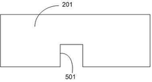
- 기판과,상기 기판의 상면에 길이 방향으로 형성된 도파로와,상기 기판의 하면에 형성된 공간 필터를 포함하여 이루어지며,상기 공간 필터는 상기 기판의 하면에 형성된 그루브로서 이 그루브를 이루는 적어도 일부의 표면에 비정질 영역 및 마이크로 크랙이 형성된 것을 특징으로 하는 집적 광학 소자.
- 제1항에 있어서, 상기 그루브는 복수 개 형성되며, 길이 방향으로 상기 기판의 1/4 지점, 1/2 지점, 3/4 지점에 형성된 것을 특징으로 하는 집적 광학 소자.
- 제1항에 있어서, 상기 그루브의 폭은 최대 500 ㎛이고, 깊이는 상기 기판 두께의 최대 70%인 것을 특징으로 하는 집적 광학 소자.
- (가) 집적 광학 소자 기판의 일 면에 그루브 (groove)를 형성하는 단계와,(나) 상기 그루브를 이루는 적어도 일부의 표면을 레이저 조사에 의해 비정질화시키고 이 비정질화된 표면에 마이크로 크랙을 형성하는 단계를 포함하여 이루어진 것을 특징으로 하는 집적 광학 소자용 공간 필터의 제조 방법.
- 제4항에 있어서, 상기 (가) 단계에서 상기 그루브는 다이싱 소우 (dicing saw), 화학적 식각, 다이아몬드 컷팅, 또는 마이크로 머시닝 (micro-machining)에 의하여 형성하는 것을 특징으로 하는 집적 광학 소자용 공간 필터의 제조 방법.
- 제4항에 있어서, 상기 (나) 단계에서 레이저의 펄스 및 출력을 조절하여 비정질화 및 마이크로 크랙의 양을 조절하는 것을 특징으로 하는 집적 광학 소자용 공간 필터의 제조 방법.
Priority Applications (1)
| Application Number | Priority Date | Filing Date | Title |
|---|---|---|---|
| KR1020070043709A KR100900898B1 (ko) | 2007-05-04 | 2007-05-04 | 집적 광학 소자 및 이에 사용되는 공간 필터의 제조 방법 |
Applications Claiming Priority (1)
| Application Number | Priority Date | Filing Date | Title |
|---|---|---|---|
| KR1020070043709A KR100900898B1 (ko) | 2007-05-04 | 2007-05-04 | 집적 광학 소자 및 이에 사용되는 공간 필터의 제조 방법 |
Publications (2)
| Publication Number | Publication Date |
|---|---|
| KR20080098257A true KR20080098257A (ko) | 2008-11-07 |
| KR100900898B1 KR100900898B1 (ko) | 2009-06-03 |
Family
ID=40285821
Family Applications (1)
| Application Number | Title | Priority Date | Filing Date |
|---|---|---|---|
| KR1020070043709A Active KR100900898B1 (ko) | 2007-05-04 | 2007-05-04 | 집적 광학 소자 및 이에 사용되는 공간 필터의 제조 방법 |
Country Status (1)
| Country | Link |
|---|---|
| KR (1) | KR100900898B1 (ko) |
Cited By (1)
| Publication number | Priority date | Publication date | Assignee | Title |
|---|---|---|---|---|
| CN108761640A (zh) * | 2018-06-12 | 2018-11-06 | 黑龙江工业学院 | 一种光纤耦合的高偏振消光比波导起偏器及其制造方法 |
Families Citing this family (1)
| Publication number | Priority date | Publication date | Assignee | Title |
|---|---|---|---|---|
| CN103760691B (zh) * | 2014-01-24 | 2016-05-11 | 东南大学 | 一种偏振态控制的多模干涉型光开关及其制备方法 |
Family Cites Families (4)
| Publication number | Priority date | Publication date | Assignee | Title |
|---|---|---|---|---|
| US5321779A (en) | 1992-11-06 | 1994-06-14 | The Charles Stark Draper Laboratory, Inc. | Optical substrate with light absorbing segments |
| US5475772A (en) | 1994-06-02 | 1995-12-12 | Honeywell Inc. | Spatial filter for improving polarization extinction ratio in a proton exchange wave guide device |
| US6351575B1 (en) | 1999-12-23 | 2002-02-26 | Litton Systems, Inc. | Multifunction integrated optics chip having improved polarization extinction ratio |
| US6418246B1 (en) | 1999-12-23 | 2002-07-09 | Litton Systems, Inc. | Lateral trenching for cross coupling suppression in integrated optics chips |
-
2007
- 2007-05-04 KR KR1020070043709A patent/KR100900898B1/ko active Active
Cited By (1)
| Publication number | Priority date | Publication date | Assignee | Title |
|---|---|---|---|---|
| CN108761640A (zh) * | 2018-06-12 | 2018-11-06 | 黑龙江工业学院 | 一种光纤耦合的高偏振消光比波导起偏器及其制造方法 |
Also Published As
| Publication number | Publication date |
|---|---|
| KR100900898B1 (ko) | 2009-06-03 |
Similar Documents
| Publication | Publication Date | Title |
|---|---|---|
| US9958608B2 (en) | Passive optical diode on semiconductor substrate | |
| JP2000314815A (ja) | コンパクト光導波路 | |
| US9778542B2 (en) | High power visible laser with a laser-fabricated nonlinear waveguide | |
| EP3100088B1 (fr) | Méthode de fabrication d'un guide d'onde optique à structure " ridge " à faibles pertes de couplage entre le guide d'onde optique à structure " ridge " et une fibre optique, et guide d'onde optique à structure " ridge " fabriqué par cette méthode | |
| US20020085824A1 (en) | Index trimming of optical waveguide devices using ultrashort laser pulses for arbitrary control of signal amplitude, phase, and polarization | |
| US20080264910A1 (en) | Process for Fabricating Optical Waveguides | |
| KR100900898B1 (ko) | 집적 광학 소자 및 이에 사용되는 공간 필터의 제조 방법 | |
| JP3895287B2 (ja) | サファイア基板の分割方法及び分割装置 | |
| US9097852B2 (en) | Multi-mode interference device | |
| WO2023286408A1 (ja) | 導波素子、光走査素子および光変調素子 | |
| JP2007003969A (ja) | 光学素子 | |
| CA2361952A1 (en) | Laser ablation of waveguide structures | |
| KR101788400B1 (ko) | 평면형 광파 회로 기반의 집적 광학 칩 | |
| KR101787209B1 (ko) | 포화 흡수체 및 그 제조 방법, 그리고 이를 이용한 펄스 레이저 장치 | |
| JP2010188370A (ja) | レーザ加工装置及びレーザ加工方法 | |
| Bado et al. | Dramatic improvements in waveguide manufacturing with femtosecond lasers | |
| JP3921987B2 (ja) | フォトニック結晶導波路及びその製造方法 | |
| Bachman et al. | Post-fabrication tuning of Silicon microring resonators by femtosecond laser modification | |
| TW201923401A (zh) | 光學構件以及其製造之方法 | |
| JPWO2014142347A1 (ja) | しみ出し光発生素子およびしみ出し光発生デバイス | |
| JP4947212B2 (ja) | 光導波路の製造方法 | |
| US20160334580A1 (en) | Optical waveguide interconnect | |
| KR20110002164A (ko) | 광섬유 코어 모드 차단기 및 그 제조 방법 | |
| Farrell | Silicon-based photonic crystal waveguides and couplers | |
| Dong et al. | Stress-induced waveguides written by femtosecond laser in phosphate glass |
Legal Events
| Date | Code | Title | Description |
|---|---|---|---|
| A201 | Request for examination | ||
| PA0109 | Patent application |
Patent event code: PA01091R01D Comment text: Patent Application Patent event date: 20070504 |
|
| PA0201 | Request for examination | ||
| PG1501 | Laying open of application | ||
| E902 | Notification of reason for refusal | ||
| PE0902 | Notice of grounds for rejection |
Comment text: Notification of reason for refusal Patent event date: 20081128 Patent event code: PE09021S01D |
|
| E701 | Decision to grant or registration of patent right | ||
| PE0701 | Decision of registration |
Patent event code: PE07011S01D Comment text: Decision to Grant Registration Patent event date: 20090525 |
|
| GRNT | Written decision to grant | ||
| PR0701 | Registration of establishment |
Comment text: Registration of Establishment Patent event date: 20090528 Patent event code: PR07011E01D |
|
| PR1002 | Payment of registration fee |
Payment date: 20090529 End annual number: 3 Start annual number: 1 |
|
| PG1601 | Publication of registration | ||
| PR1001 | Payment of annual fee |
Payment date: 20120430 Start annual number: 4 End annual number: 4 |
|
| FPAY | Annual fee payment |
Payment date: 20130502 Year of fee payment: 5 |
|
| PR1001 | Payment of annual fee |
Payment date: 20130502 Start annual number: 5 End annual number: 5 |
|
| FPAY | Annual fee payment |
Payment date: 20140502 Year of fee payment: 6 |
|
| PR1001 | Payment of annual fee |
Payment date: 20140502 Start annual number: 6 End annual number: 6 |
|
| FPAY | Annual fee payment |
Payment date: 20150504 Year of fee payment: 7 |
|
| PR1001 | Payment of annual fee |
Payment date: 20150504 Start annual number: 7 End annual number: 7 |
|
| FPAY | Annual fee payment |
Payment date: 20190502 Year of fee payment: 11 |
|
| PR1001 | Payment of annual fee |
Payment date: 20190502 Start annual number: 11 End annual number: 11 |
|
| PR1001 | Payment of annual fee |
Payment date: 20200504 Start annual number: 12 End annual number: 12 |
|
| PR1001 | Payment of annual fee |
Payment date: 20210504 Start annual number: 13 End annual number: 13 |