KR20080098257A - Integrated optical device and method of manufacturing spatial filter used therein - Google Patents
Integrated optical device and method of manufacturing spatial filter used therein Download PDFInfo
- Publication number
- KR20080098257A KR20080098257A KR1020070043709A KR20070043709A KR20080098257A KR 20080098257 A KR20080098257 A KR 20080098257A KR 1020070043709 A KR1020070043709 A KR 1020070043709A KR 20070043709 A KR20070043709 A KR 20070043709A KR 20080098257 A KR20080098257 A KR 20080098257A
- Authority
- KR
- South Korea
- Prior art keywords
- substrate
- integrated optical
- groove
- optical device
- spatial filter
- Prior art date
- Legal status (The legal status is an assumption and is not a legal conclusion. Google has not performed a legal analysis and makes no representation as to the accuracy of the status listed.)
- Granted
Links
- 230000003287 optical effect Effects 0.000 title claims abstract description 33
- 238000004519 manufacturing process Methods 0.000 title claims abstract description 7
- 239000000758 substrate Substances 0.000 claims abstract description 39
- 238000003486 chemical etching Methods 0.000 claims description 3
- 238000005520 cutting process Methods 0.000 claims description 2
- 229910003460 diamond Inorganic materials 0.000 claims description 2
- 239000010432 diamond Substances 0.000 claims description 2
- 238000005459 micromachining Methods 0.000 claims description 2
- 238000000034 method Methods 0.000 abstract description 13
- 230000010287 polarization Effects 0.000 abstract description 10
- 230000000171 quenching effect Effects 0.000 abstract description 5
- 239000013307 optical fiber Substances 0.000 description 10
- GQYHUHYESMUTHG-UHFFFAOYSA-N lithium niobate Chemical compound [Li+].[O-][Nb](=O)=O GQYHUHYESMUTHG-UHFFFAOYSA-N 0.000 description 8
- 230000015572 biosynthetic process Effects 0.000 description 6
- 230000008033 biological extinction Effects 0.000 description 4
- 238000010586 diagram Methods 0.000 description 3
- 238000010791 quenching Methods 0.000 description 3
- 230000000694 effects Effects 0.000 description 2
- 238000012986 modification Methods 0.000 description 2
- 230000004048 modification Effects 0.000 description 2
- 238000012545 processing Methods 0.000 description 2
- 239000000126 substance Substances 0.000 description 2
- 229910013641 LiNbO 3 Inorganic materials 0.000 description 1
- 230000002159 abnormal effect Effects 0.000 description 1
- 230000000903 blocking effect Effects 0.000 description 1
- 230000015556 catabolic process Effects 0.000 description 1
- 238000007796 conventional method Methods 0.000 description 1
- 239000013078 crystal Substances 0.000 description 1
- 230000003247 decreasing effect Effects 0.000 description 1
- 238000006731 degradation reaction Methods 0.000 description 1
- 238000005530 etching Methods 0.000 description 1
- 230000003993 interaction Effects 0.000 description 1
- 230000001678 irradiating effect Effects 0.000 description 1
- 239000000463 material Substances 0.000 description 1
- 238000003672 processing method Methods 0.000 description 1
- 230000001902 propagating effect Effects 0.000 description 1
- 238000012546 transfer Methods 0.000 description 1
- 238000009834 vaporization Methods 0.000 description 1
- 230000008016 vaporization Effects 0.000 description 1
- 238000001039 wet etching Methods 0.000 description 1
Images


Classifications
-
- G—PHYSICS
- G02—OPTICS
- G02B—OPTICAL ELEMENTS, SYSTEMS OR APPARATUS
- G02B6/00—Light guides; Structural details of arrangements comprising light guides and other optical elements, e.g. couplings
- G02B6/10—Light guides; Structural details of arrangements comprising light guides and other optical elements, e.g. couplings of the optical waveguide type
- G02B6/12—Light guides; Structural details of arrangements comprising light guides and other optical elements, e.g. couplings of the optical waveguide type of the integrated circuit kind
- G02B6/126—Light guides; Structural details of arrangements comprising light guides and other optical elements, e.g. couplings of the optical waveguide type of the integrated circuit kind using polarisation effects
-
- G—PHYSICS
- G02—OPTICS
- G02B—OPTICAL ELEMENTS, SYSTEMS OR APPARATUS
- G02B6/00—Light guides; Structural details of arrangements comprising light guides and other optical elements, e.g. couplings
- G02B6/0001—Light guides; Structural details of arrangements comprising light guides and other optical elements, e.g. couplings specially adapted for lighting devices or systems
- G02B6/0011—Light guides; Structural details of arrangements comprising light guides and other optical elements, e.g. couplings specially adapted for lighting devices or systems the light guides being planar or of plate-like form
- G02B6/0013—Means for improving the coupling-in of light from the light source into the light guide
- G02B6/0015—Means for improving the coupling-in of light from the light source into the light guide provided on the surface of the light guide or in the bulk of it
- G02B6/0016—Grooves, prisms, gratings, scattering particles or rough surfaces
-
- G—PHYSICS
- G02—OPTICS
- G02B—OPTICAL ELEMENTS, SYSTEMS OR APPARATUS
- G02B6/00—Light guides; Structural details of arrangements comprising light guides and other optical elements, e.g. couplings
- G02B6/10—Light guides; Structural details of arrangements comprising light guides and other optical elements, e.g. couplings of the optical waveguide type
- G02B6/12—Light guides; Structural details of arrangements comprising light guides and other optical elements, e.g. couplings of the optical waveguide type of the integrated circuit kind
- G02B6/122—Basic optical elements, e.g. light-guiding paths
- G02B6/125—Bends, branchings or intersections
-
- G—PHYSICS
- G02—OPTICS
- G02B—OPTICAL ELEMENTS, SYSTEMS OR APPARATUS
- G02B6/00—Light guides; Structural details of arrangements comprising light guides and other optical elements, e.g. couplings
- G02B6/10—Light guides; Structural details of arrangements comprising light guides and other optical elements, e.g. couplings of the optical waveguide type
- G02B6/12—Light guides; Structural details of arrangements comprising light guides and other optical elements, e.g. couplings of the optical waveguide type of the integrated circuit kind
- G02B2006/12083—Constructional arrangements
- G02B2006/12109—Filter
Landscapes
- Physics & Mathematics (AREA)
- General Physics & Mathematics (AREA)
- Optics & Photonics (AREA)
- Engineering & Computer Science (AREA)
- Microelectronics & Electronic Packaging (AREA)
- Optical Integrated Circuits (AREA)
Abstract
본 발명은 높은 편광 소광 특성을 지니는 집적 광학 소자 및 이에 사용되는 공간 필터의 제조 방법에 관한 것이다. 본 발명은 기판의 상면에 길이 방향으로 도파로가 형성되고, 상기 기판의 하면에 그루브가 형성되며, 이 그루브를 이루는 적어도 일부의 표면에 비정질 영역 및 마이크로 크랙이 형성된 것을 특징으로 하는 집적 광학 소자를 제공한다. 또한, 본 발명은 집적 광학 소자 기판의 일 면에 그루브를 형성하는 단계와, 상기 그루브를 이루는 적어도 일부의 표면을 레이저 조사에 의해 비정질화시키고 이 비정질화된 표면에 마이크로 크랙을 형성하는 단계를 포함하여 이루어진 것을 특징으로 하는 집적 광학 소자용 공간 필터의 제조 방법을 제공한다.BACKGROUND OF THE INVENTION 1. Field of the Invention The present invention relates to integrated optical devices having high polarization quenching properties and methods of manufacturing spatial filters used therein. The present invention provides an integrated optical device, wherein a waveguide is formed in a longitudinal direction on a top surface of a substrate, grooves are formed on a bottom surface of the substrate, and amorphous regions and microcracks are formed on at least a portion of the surface of the substrate. do. The present invention also includes forming a groove on one surface of an integrated optical device substrate, and amorphizing at least a portion of the surface constituting the groove by laser irradiation and forming microcracks on the amorphous surface. It provides a manufacturing method of a spatial filter for an integrated optical device, characterized in that made.
Description
도 1은 집적 광학 소자를 개략적으로 나타낸 사시도이다.1 is a perspective view schematically showing an integrated optical device.
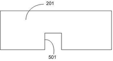
도 2는 공간 필터에 의한 TM 모드 제거 방법을 나타내는 개념도이다.2 is a conceptual diagram illustrating a method of removing a TM mode by a spatial filter.
도 3a는 다이싱 소우에 의해 형성된 그루브의 개념도이고, 도 3b는 레이저 조사에 의해 생성된 리튬니오베이트 기판 면의 비정질 영역 및 마이크로 크랙을 나타내는 개념도이다.3A is a conceptual diagram of a groove formed by dicing saw, and FIG. 3B is a conceptual diagram illustrating an amorphous region and micro cracks on a surface of a lithium niobate substrate generated by laser irradiation.
* 도면의 주요 부분에 대한 부호의 설명 *Explanation of symbols on the main parts of the drawings
101: 입력단 광섬유 102: 출력단 광섬유101: input end optical fiber 102: output end optical fiber
201: 리튬니오베이트 기판 301: 광도파로201: lithium niobate substrate 301: optical waveguide
401,402: TM 모드 광 501, 501a, 501b, 501c: 그루브401, 402:
601: 비정질 영역 701: 마이크로 크랙601: amorphous region 701: microcracks
본 발명은 높은 편광 소광 특성을 지니는 집적 광학 소자 및 이에 사용되는 공간 필터의 제조 방법에 관한 것이다. BACKGROUND OF THE INVENTION 1. Field of the Invention The present invention relates to integrated optical devices having high polarization quenching properties and methods of manufacturing spatial filters used therein.
양자 교환 (proton exchange) 방법에 의해 제조된 광도파로를 가지는 집적 광학 소자에 있어서, 기판으로 이용한 리튬니오베이트 (LiNbO3)는 단일 광축 결정 (uniaxial crystal)으로 빛의 편광 방향에 따라 굴절률이 다르게 보이는 성질이 있다. 리튬니오베이트 기판에 양자 교환을 하게 되면 이상 굴절률은 증가하는 반면, 정상 굴절률은 감소하게 된다. In an integrated optical device having an optical waveguide manufactured by a proton exchange method, lithium niobate (LiNbO 3 ) used as a substrate is a uniaxial crystal, and its refractive index is different depending on the polarization direction of light. There is a nature. Proton exchange on the lithium niobate substrate increases the abnormal refractive index while decreasing the normal refractive index.
양자 교환에 의해 증가된 이상굴절률을 보는 빛만이 도파되는데, X-cut, Y-cut 리튬니오베이트 기판의 경우 TE (Transverse Electric) 모드 광 (light)만이 도파로를 따라 도파된다. 도파되지 못하는 모드의 빛은 리튬니오베이트 기판 내부에서 대부분 소멸된다. 그러나, 일부 TM (Transverse Magnetic) 모드 성분이 기판 바닥면에서 반사되어 집적 광학 소자 출력단 광섬유에 입사되어, 집적 광학 소자 편광 소광 특성 저하를 초래하게 된다. TM 모드 성분의 출력단 광섬유로의 진행을 막는 방법으로 리튬니오베이트 기판 바닥면에 그루브 (groove)를 형성하고, 그루브를 공간 필터로 이용하는 방법이 있다. Only light that sees an increased refractive index increased by proton exchange is guided. In the case of X-cut and Y-cut lithium niobate substrates, only TE (Transverse Electric) mode light is guided along the waveguide. Light in the non-guided mode is mostly dissipated inside the lithium niobate substrate. However, some transverse magnetic (TM) mode components are reflected at the bottom surface of the substrate and are incident on the integrated optical element output optical fiber, resulting in degradation of the integrated optical element polarization quenching characteristics. As a method of preventing the TM mode component from advancing to the optical fiber, a groove is formed on the bottom surface of the lithium niobate substrate, and the groove is used as a space filter.
그루브를 형성하는 방법으로는 물리적 가공 방법으로 다이싱 소우 (dicing saw), 레이저 가공 등이 있으며, 화학적 방법으로는 케미컬을 이용한 습식 식각 방법이 있다. Grooves are formed by dicing saws, lasers, etc. as physical processing methods, and chemical etching methods include wet etching using chemicals.
그런데, 종래의 기술에 의한 다이싱 소우에 의한 그루브 형성은, 가공 면에서의 TM 모드 성분 재반사에 의해 편광 소광 특성이 만족스럽지 않다. By the way, the groove formation by dicing saw by a conventional technique is not satisfactory in polarization extinction characteristic by TM-mode component rereflection in a process surface.
또한, 레이저 가공에 의한 그루브 형성은, 레이저의 작은 스폿 (spot) 크기 로 인해 그루브 형성에 많은 시간이 소요되며, 그루브의 깊이가 일정하지 않아 Y형 광 분할기 특성을 가지는 집적 광학 소자의 출력단 두 개의 편광 소광 특성이 일치하지 않는 경우가 빈번하다. In addition, groove formation by laser processing takes a lot of time for groove formation due to the small spot size of the laser, and because the depth of the groove is not constant, two output stages of the integrated optical element having Y-type light splitter characteristics are obtained. Frequently, polarization extinction characteristics do not coincide.
또한, 케미컬을 이용한 습식 방법에 의한 그루브 형성은, 별도의 식각용 마스크를 필요로 하는 등의 공정 절차가 복잡하다는 단점을 가지고 있다.In addition, groove formation by a wet method using a chemical has a disadvantage in that a process procedure such as requiring a separate etching mask is complicated.
본 발명은 이러한 종래의 문제점들을 해결하기 위하여 안출된 것으로서, 본 발명은 TM 모드 성분의 출력단 광섬유로의 진행을 막기 위해 기판 바닥면에 그루브를 형성하되, 이 그루브를 이루는 표면을 레이저 조사에 의해 개질시킴으로써, 상기 그루브의 공간 필터로서의 성능을 향상시키는 데 그 목적이 있다.The present invention has been made to solve the above-mentioned problems, the present invention is to form a groove on the bottom surface of the substrate to prevent the progression of the TM mode component to the output optical fiber, the surface forming the groove is modified by laser irradiation This aims to improve the performance of the grooves as a spatial filter.
이러한 목적은 다음의 본 발명의 구성에 의하여 달성될 수 있다.This object can be achieved by the following configuration of the present invention.
(1) 기판과, (1) a substrate;
상기 기판의 상면에 길이 방향으로 형성된 도파로와, A waveguide formed in a longitudinal direction on an upper surface of the substrate,
상기 기판의 하면에 형성된 공간 필터를 포함하여 이루어지며, Including a space filter formed on the lower surface of the substrate,
상기 공간 필터는 상기 기판의 하면에 형성된 그루브로서 이 그루브를 이루는 적어도 일부의 표면에 비정질 영역 및 마이크로 크랙이 형성된 것을 특징으로 하는 집적 광학 소자.The spatial filter is a groove formed on a lower surface of the substrate, wherein an amorphous region and micro cracks are formed on at least a portion of the surface of the substrate.
(2) (가) 집적 광학 소자 기판의 일 면에 그루브 (groove)를 형성하는 단계와, (2) (a) forming a groove on one surface of the integrated optical element substrate,
(나) 상기 그루브를 이루는 적어도 일부의 표면을 레이저 조사에 의해 비정질화시키고 이 비정질화된 표면에 마이크로 크랙을 형성하는 단계를 포함하여 이루어진 것을 특징으로 하는 집적 광학 소자용 공간 필터의 제조 방법.(B) amorphizing at least a portion of the surface constituting the groove by laser irradiation, and forming microcracks on the amorphous surface.
이하, 첨부 도면에 따라 본 발명의 최선의 실시 상태를 상세히 설명하겠다.BEST MODE FOR CARRYING OUT THE INVENTION Hereinafter, the best mode of carrying out the present invention will be described in detail with reference to the accompanying drawings.
도 1에 의하면, 본 발명의 일 실시예에 따른 집적 광학 소자는 리튬니오베이트 기판(201)과, 이 기판(201)의 상면에 길이 방향으로 형성된 광도파로(301)와, 상기 기판(201)의 하면에 형성된 공간 필터(도시되지 않음)를 포함하여 이루어진다. 상기 광도파로(301)의 입력단과 출력단은 각각 입력단 광섬유(101)와 출력단 광섬유(102)와 연결된다.Referring to FIG. 1, an integrated optical device according to an exemplary embodiment includes a
여기서, 상기 공간 필터는 상기 기판(201)의 하면에 형성된 그루브로서 이 그루브를 이루는 적어도 일부의 표면에 비정질 영역 및 마이크로 크랙이 형성된 것을 특징으로 한다. 이에 따라, 출력단 광섬유로 진행하는 TM 모드가 공간 필터의 비정질화된 표면과 마이크로 크랙에 의해 산란 및 흡수되어 TM 모드 진행이 효과적으로 억제된다. 따라서, 본 발명에 의하면, 높은 편광 소광 특성을 가지는 집적 광학 소자를 얻을 수 있다.Here, the spatial filter is a groove formed on the lower surface of the
도 2는 도 1의 기판 방향 단면을 나타낸 도면이다. 도 2에 나타낸 바와 같이, 상기 그루브의 위치는, TM 모드 광(401, 402)의 효과적인 차단을 위해, 집적 광학 소자의 길이 방향으로 가운데 지점(501b)을 포함하여, 1/4 지점(501a)과, 3/4 지점(501c)을 선택하는 것이 바람직하다.FIG. 2 is a cross-sectional view of the substrate in FIG. 1. As shown in FIG. 2, the position of the groove includes a
또한, 상기 그루브의 깊이와 폭은, 집적 광학 소자가 파손되지 않는 경우라 면, 깊이는 깊을수록, 폭은 넓을수록 편광 소광 특성의 향상이 기대되나, 바람직하게는 폭은 500 ㎛ 이하, 깊이는 기판 두께의 70%를 넘지 않는 것이 좋다.In addition, the depth and width of the groove are expected to improve the polarization quenching characteristics as the depth is deeper and the width is wider when the integrated optical device is not damaged, but the width is preferably 500 μm or less and the depth is It is recommended not to exceed 70% of the substrate thickness.
이하에서는, 도 3a 및 도 3b에 따라 본 발명에 의한 집적 광학 소자용 공간 필터를 제조하는 방법에 대하여 상세히 설명하겠다.Hereinafter, a method of manufacturing a spatial filter for an integrated optical device according to the present invention will be described in detail with reference to FIGS. 3A and 3B.
먼저, 집적 광학 소자 기판(201)의 일 면에 그루브(501)를 형성한다 (도 3a). First, a
본 발명에서, 상기 그루브(501)는 다이싱 소우 (dicing saw), 화학적 식각, 다이아몬드 컷팅, 또는 마이크로 머시닝 (micro-machining)에 의하여 형성할 수 있다. In the present invention, the
이 그루브 형성 공정은 양자 교환을 이용한 광도파로(301) 형성 전 또는 후 언제라도 가능하나, 입력단 광섬유(101)와 출력단 광섬유(102)를 집적 광학 소자와 접합하는 공정 이전에 이루어져야 한다.This groove forming process may be performed at any time before or after the formation of the
그 다음, 상기 그루브(501)를 이루는 적어도 일부의 표면을 레이저 조사에 의해 비정질화시키고 이 비정질화된 표면에 마이크로 크랙(701)을 형성한다 (도 3b). 도면 부호 601은 레이저 조사에 의하여 표면이 개질된 비정질 영역을 나타낸다. Next, at least a portion of the surface constituting the
상기 기판(201)의 바닥면에 형성된 그루브(501)를 이루는 표면에 레이저를 조사함으로써, 가공 부분 주변에 열 변형을 발생시켜 상기 그루브 표면을 비정질화시키고, 열 왜곡에 의한 파손을 유도하여 마이크로 크랙 (micro crack)을 형성한다.By irradiating the surface of the
예컨대, 다이싱 소우에 의해 형성된 그루브 면에 CO2 레이저 또는 Nd:YAG 레이저를 조사한다. 레이저 펄스는 기판에 연속적으로 흡수되며, 일정 레벨의 열 에너지를 흡수한 후에 기판을 순간적으로 기화시킨다. 상호 작용에 의해 기화한 물질이 웨이퍼에서 열 에너지를 빼앗으므로 기판으로의 열 영향을 최소화할 수 있다. 레이저의 스폿 사이즈가 수 ㎛에 불과하므로, 집적 광학 소자는 프로그래밍된 자동 이송 장치 등을 이용하여 레이저 스폿 사이즈에 비해 넓은 면적을 갖는 그루브 표면에 대한 레이저 가공을 수월하게 시행할 수 있다.For example, a groove surface formed by dicing saw is irradiated with a CO 2 laser or an Nd: YAG laser. The laser pulses are continuously absorbed by the substrate and vaporize the substrate instantly after absorbing a certain level of thermal energy. The vaporization of the material by interaction deprives the wafer of thermal energy, minimizing the thermal effect on the substrate. Since the spot size of the laser is only a few micrometers, the integrated optical device can easily perform laser processing on the groove surface having a larger area than the laser spot size by using a programmed automatic transfer device or the like.
이때, 집적 광학 소자가 물리적으로 파손되거나, 또는 광도파로 특성에 영향을 미치지 않는 범위에서 레이저의 펄스와 출력을 조절하여 상기 그루브 표면에 레이저의 열 에너지에 의한 비정질 영역(601) 형성 및 마이크로 크랙(701) 형성 등과 같은 표면 개질 효과가 크게 발생할 수 있도록 조절한다. 마이크로 크랙 또는 비정질 영역이 클수록 집적 광학 소자의 편광 소광 특성은 향상된다.At this time, by forming the
이상, 본 발명을 도시된 예를 중심으로 하여 설명하였으나 이는 예시에 지나지 아니하며, 본 발명은 본 발명의 기술분야에서 통상의 지식을 가진 자에게 자명한 다양한 변형 및 균등한 기타의 실시예를 수행할 수 있다는 사실을 이해하여야 한다. In the above, the present invention has been described with reference to the illustrated examples, which are merely examples, and the present invention may be embodied in various modifications and other embodiments that are obvious to those skilled in the art. Understand that you can.
본 발명에 의하면, 다이싱 소우 방법 등에 의해 기판 하면에 그루브를 형성하여 작업 시간을 단축시킬 수 있고, 레이저 조사에 의해 그루브 표면에 비정질 영 역 및 마이크로 크랙을 형성하여 집적 광학 소자의 편광 소광 특성을 향상시킬 수 있게 된다.According to the present invention, grooves can be formed on the bottom surface of the substrate by a dicing saw method or the like to shorten the working time, and amorphous regions and microcracks are formed on the groove surface by laser irradiation to improve the polarization extinction characteristics of the integrated optical device. It can be improved.
Claims (6)
Priority Applications (1)
| Application Number | Priority Date | Filing Date | Title |
|---|---|---|---|
| KR1020070043709A KR100900898B1 (en) | 2007-05-04 | 2007-05-04 | Integrated optical device and method of manufacturing spatial filter used therein |
Applications Claiming Priority (1)
| Application Number | Priority Date | Filing Date | Title |
|---|---|---|---|
| KR1020070043709A KR100900898B1 (en) | 2007-05-04 | 2007-05-04 | Integrated optical device and method of manufacturing spatial filter used therein |
Publications (2)
| Publication Number | Publication Date |
|---|---|
| KR20080098257A true KR20080098257A (en) | 2008-11-07 |
| KR100900898B1 KR100900898B1 (en) | 2009-06-03 |
Family
ID=40285821
Family Applications (1)
| Application Number | Title | Priority Date | Filing Date |
|---|---|---|---|
| KR1020070043709A Active KR100900898B1 (en) | 2007-05-04 | 2007-05-04 | Integrated optical device and method of manufacturing spatial filter used therein |
Country Status (1)
| Country | Link |
|---|---|
| KR (1) | KR100900898B1 (en) |
Cited By (1)
| Publication number | Priority date | Publication date | Assignee | Title |
|---|---|---|---|---|
| CN108761640A (en) * | 2018-06-12 | 2018-11-06 | 黑龙江工业学院 | A kind of high polarization extinction ratio waveguide polarizer and its manufacturing method of fiber coupling |
Families Citing this family (1)
| Publication number | Priority date | Publication date | Assignee | Title |
|---|---|---|---|---|
| CN103760691B (en) * | 2014-01-24 | 2016-05-11 | 东南大学 | Multi-mode interference-type photoswitch of a kind of polarization state control and preparation method thereof |
Family Cites Families (4)
| Publication number | Priority date | Publication date | Assignee | Title |
|---|---|---|---|---|
| US5321779A (en) | 1992-11-06 | 1994-06-14 | The Charles Stark Draper Laboratory, Inc. | Optical substrate with light absorbing segments |
| US5475772A (en) | 1994-06-02 | 1995-12-12 | Honeywell Inc. | Spatial filter for improving polarization extinction ratio in a proton exchange wave guide device |
| US6351575B1 (en) | 1999-12-23 | 2002-02-26 | Litton Systems, Inc. | Multifunction integrated optics chip having improved polarization extinction ratio |
| US6418246B1 (en) | 1999-12-23 | 2002-07-09 | Litton Systems, Inc. | Lateral trenching for cross coupling suppression in integrated optics chips |
-
2007
- 2007-05-04 KR KR1020070043709A patent/KR100900898B1/en active Active
Cited By (1)
| Publication number | Priority date | Publication date | Assignee | Title |
|---|---|---|---|---|
| CN108761640A (en) * | 2018-06-12 | 2018-11-06 | 黑龙江工业学院 | A kind of high polarization extinction ratio waveguide polarizer and its manufacturing method of fiber coupling |
Also Published As
| Publication number | Publication date |
|---|---|
| KR100900898B1 (en) | 2009-06-03 |
Similar Documents
| Publication | Publication Date | Title |
|---|---|---|
| US9958608B2 (en) | Passive optical diode on semiconductor substrate | |
| JP2000314815A (en) | Compact optical waveguide | |
| US9778542B2 (en) | High power visible laser with a laser-fabricated nonlinear waveguide | |
| EP3100088B1 (en) | Method for producing a ridge optical waveguide having low coupling losses between the ridge optical waveguide and an optical fibre, and a ridge optical waveguide made using this method | |
| US20020085824A1 (en) | Index trimming of optical waveguide devices using ultrashort laser pulses for arbitrary control of signal amplitude, phase, and polarization | |
| US20080264910A1 (en) | Process for Fabricating Optical Waveguides | |
| KR100900898B1 (en) | Integrated optical device and method of manufacturing spatial filter used therein | |
| JP3895287B2 (en) | Method and apparatus for dividing sapphire substrate | |
| US9097852B2 (en) | Multi-mode interference device | |
| WO2023286408A1 (en) | Waveguide element, optical scanning element and optical modulation element | |
| JP2007003969A (en) | Optical element | |
| CA2361952A1 (en) | Laser ablation of waveguide structures | |
| KR101788400B1 (en) | Planar lightwave circuit based integrated optical chip | |
| KR101787209B1 (en) | Saturable absorber and manufacturing method thereof, and pulse laser device using the same | |
| JP2010188370A (en) | Laser beam machining apparatus and laser beam machining method | |
| Bado et al. | Dramatic improvements in waveguide manufacturing with femtosecond lasers | |
| JP3921987B2 (en) | Photonic crystal waveguide and manufacturing method thereof | |
| Bachman et al. | Post-fabrication tuning of Silicon microring resonators by femtosecond laser modification | |
| TW201923401A (en) | Optical component and method for the production thereof | |
| JPWO2014142347A1 (en) | Exudation light generating element and exudation light generating device | |
| JP4947212B2 (en) | Manufacturing method of optical waveguide | |
| US20160334580A1 (en) | Optical waveguide interconnect | |
| KR20110002164A (en) | Fiber Optic Core Mode Breaker and Manufacturing Method Thereof | |
| Farrell | Silicon-based photonic crystal waveguides and couplers | |
| Dong et al. | Stress-induced waveguides written by femtosecond laser in phosphate glass |
Legal Events
| Date | Code | Title | Description |
|---|---|---|---|
| A201 | Request for examination | ||
| PA0109 | Patent application |
Patent event code: PA01091R01D Comment text: Patent Application Patent event date: 20070504 |
|
| PA0201 | Request for examination | ||
| PG1501 | Laying open of application | ||
| E902 | Notification of reason for refusal | ||
| PE0902 | Notice of grounds for rejection |
Comment text: Notification of reason for refusal Patent event date: 20081128 Patent event code: PE09021S01D |
|
| E701 | Decision to grant or registration of patent right | ||
| PE0701 | Decision of registration |
Patent event code: PE07011S01D Comment text: Decision to Grant Registration Patent event date: 20090525 |
|
| GRNT | Written decision to grant | ||
| PR0701 | Registration of establishment |
Comment text: Registration of Establishment Patent event date: 20090528 Patent event code: PR07011E01D |
|
| PR1002 | Payment of registration fee |
Payment date: 20090529 End annual number: 3 Start annual number: 1 |
|
| PG1601 | Publication of registration | ||
| PR1001 | Payment of annual fee |
Payment date: 20120430 Start annual number: 4 End annual number: 4 |
|
| FPAY | Annual fee payment |
Payment date: 20130502 Year of fee payment: 5 |
|
| PR1001 | Payment of annual fee |
Payment date: 20130502 Start annual number: 5 End annual number: 5 |
|
| FPAY | Annual fee payment |
Payment date: 20140502 Year of fee payment: 6 |
|
| PR1001 | Payment of annual fee |
Payment date: 20140502 Start annual number: 6 End annual number: 6 |
|
| FPAY | Annual fee payment |
Payment date: 20150504 Year of fee payment: 7 |
|
| PR1001 | Payment of annual fee |
Payment date: 20150504 Start annual number: 7 End annual number: 7 |
|
| FPAY | Annual fee payment |
Payment date: 20190502 Year of fee payment: 11 |
|
| PR1001 | Payment of annual fee |
Payment date: 20190502 Start annual number: 11 End annual number: 11 |
|
| PR1001 | Payment of annual fee |
Payment date: 20200504 Start annual number: 12 End annual number: 12 |
|
| PR1001 | Payment of annual fee |
Payment date: 20210504 Start annual number: 13 End annual number: 13 |