KR20070080098A - Liquid crystal display - Google Patents
Liquid crystal display Download PDFInfo
- Publication number
- KR20070080098A KR20070080098A KR1020060011211A KR20060011211A KR20070080098A KR 20070080098 A KR20070080098 A KR 20070080098A KR 1020060011211 A KR1020060011211 A KR 1020060011211A KR 20060011211 A KR20060011211 A KR 20060011211A KR 20070080098 A KR20070080098 A KR 20070080098A
- Authority
- KR
- South Korea
- Prior art keywords
- electrode
- storage
- width
- conductor
- liquid crystal
- Prior art date
- Legal status (The legal status is an assumption and is not a legal conclusion. Google has not performed a legal analysis and makes no representation as to the accuracy of the status listed.)
- Ceased
Links
Images


Classifications
-
- G—PHYSICS
- G02—OPTICS
- G02F—OPTICAL DEVICES OR ARRANGEMENTS FOR THE CONTROL OF LIGHT BY MODIFICATION OF THE OPTICAL PROPERTIES OF THE MEDIA OF THE ELEMENTS INVOLVED THEREIN; NON-LINEAR OPTICS; FREQUENCY-CHANGING OF LIGHT; OPTICAL LOGIC ELEMENTS; OPTICAL ANALOGUE/DIGITAL CONVERTERS
- G02F1/00—Devices or arrangements for the control of the intensity, colour, phase, polarisation or direction of light arriving from an independent light source, e.g. switching, gating or modulating; Non-linear optics
- G02F1/01—Devices or arrangements for the control of the intensity, colour, phase, polarisation or direction of light arriving from an independent light source, e.g. switching, gating or modulating; Non-linear optics for the control of the intensity, phase, polarisation or colour
- G02F1/13—Devices or arrangements for the control of the intensity, colour, phase, polarisation or direction of light arriving from an independent light source, e.g. switching, gating or modulating; Non-linear optics for the control of the intensity, phase, polarisation or colour based on liquid crystals, e.g. single liquid crystal display cells
- G02F1/133—Constructional arrangements; Operation of liquid crystal cells; Circuit arrangements
- G02F1/1333—Constructional arrangements; Manufacturing methods
- G02F1/1337—Surface-induced orientation of the liquid crystal molecules, e.g. by alignment layers
- G02F1/133707—Structures for producing distorted electric fields, e.g. bumps, protrusions, recesses, slits in pixel electrodes
-
- G—PHYSICS
- G01—MEASURING; TESTING
- G01N—INVESTIGATING OR ANALYSING MATERIALS BY DETERMINING THEIR CHEMICAL OR PHYSICAL PROPERTIES
- G01N19/00—Investigating materials by mechanical methods
- G01N19/10—Measuring moisture content, e.g. by measuring change in length of hygroscopic filament; Hygrometers
-
- F—MECHANICAL ENGINEERING; LIGHTING; HEATING; WEAPONS; BLASTING
- F25—REFRIGERATION OR COOLING; COMBINED HEATING AND REFRIGERATION SYSTEMS; HEAT PUMP SYSTEMS; MANUFACTURE OR STORAGE OF ICE; LIQUEFACTION SOLIDIFICATION OF GASES
- F25B—REFRIGERATION MACHINES, PLANTS OR SYSTEMS; COMBINED HEATING AND REFRIGERATION SYSTEMS; HEAT PUMP SYSTEMS
- F25B45/00—Arrangements for charging or discharging refrigerant
-
- G—PHYSICS
- G02—OPTICS
- G02F—OPTICAL DEVICES OR ARRANGEMENTS FOR THE CONTROL OF LIGHT BY MODIFICATION OF THE OPTICAL PROPERTIES OF THE MEDIA OF THE ELEMENTS INVOLVED THEREIN; NON-LINEAR OPTICS; FREQUENCY-CHANGING OF LIGHT; OPTICAL LOGIC ELEMENTS; OPTICAL ANALOGUE/DIGITAL CONVERTERS
- G02F1/00—Devices or arrangements for the control of the intensity, colour, phase, polarisation or direction of light arriving from an independent light source, e.g. switching, gating or modulating; Non-linear optics
- G02F1/01—Devices or arrangements for the control of the intensity, colour, phase, polarisation or direction of light arriving from an independent light source, e.g. switching, gating or modulating; Non-linear optics for the control of the intensity, phase, polarisation or colour
- G02F1/13—Devices or arrangements for the control of the intensity, colour, phase, polarisation or direction of light arriving from an independent light source, e.g. switching, gating or modulating; Non-linear optics for the control of the intensity, phase, polarisation or colour based on liquid crystals, e.g. single liquid crystal display cells
- G02F1/133—Constructional arrangements; Operation of liquid crystal cells; Circuit arrangements
- G02F1/1333—Constructional arrangements; Manufacturing methods
- G02F1/1343—Electrodes
- G02F1/134309—Electrodes characterised by their geometrical arrangement
-
- G—PHYSICS
- G02—OPTICS
- G02F—OPTICAL DEVICES OR ARRANGEMENTS FOR THE CONTROL OF LIGHT BY MODIFICATION OF THE OPTICAL PROPERTIES OF THE MEDIA OF THE ELEMENTS INVOLVED THEREIN; NON-LINEAR OPTICS; FREQUENCY-CHANGING OF LIGHT; OPTICAL LOGIC ELEMENTS; OPTICAL ANALOGUE/DIGITAL CONVERTERS
- G02F1/00—Devices or arrangements for the control of the intensity, colour, phase, polarisation or direction of light arriving from an independent light source, e.g. switching, gating or modulating; Non-linear optics
- G02F1/01—Devices or arrangements for the control of the intensity, colour, phase, polarisation or direction of light arriving from an independent light source, e.g. switching, gating or modulating; Non-linear optics for the control of the intensity, phase, polarisation or colour
- G02F1/13—Devices or arrangements for the control of the intensity, colour, phase, polarisation or direction of light arriving from an independent light source, e.g. switching, gating or modulating; Non-linear optics for the control of the intensity, phase, polarisation or colour based on liquid crystals, e.g. single liquid crystal display cells
- G02F1/133—Constructional arrangements; Operation of liquid crystal cells; Circuit arrangements
- G02F1/136—Liquid crystal cells structurally associated with a semi-conducting layer or substrate, e.g. cells forming part of an integrated circuit
- G02F1/1362—Active matrix addressed cells
- G02F1/136213—Storage capacitors associated with the pixel electrode
-
- F—MECHANICAL ENGINEERING; LIGHTING; HEATING; WEAPONS; BLASTING
- F25—REFRIGERATION OR COOLING; COMBINED HEATING AND REFRIGERATION SYSTEMS; HEAT PUMP SYSTEMS; MANUFACTURE OR STORAGE OF ICE; LIQUEFACTION SOLIDIFICATION OF GASES
- F25B—REFRIGERATION MACHINES, PLANTS OR SYSTEMS; COMBINED HEATING AND REFRIGERATION SYSTEMS; HEAT PUMP SYSTEMS
- F25B2345/00—Details for charging or discharging refrigerants; Service stations therefor
- F25B2345/003—Control issues for charging or collecting refrigerant to or from a cycle
-
- G—PHYSICS
- G02—OPTICS
- G02F—OPTICAL DEVICES OR ARRANGEMENTS FOR THE CONTROL OF LIGHT BY MODIFICATION OF THE OPTICAL PROPERTIES OF THE MEDIA OF THE ELEMENTS INVOLVED THEREIN; NON-LINEAR OPTICS; FREQUENCY-CHANGING OF LIGHT; OPTICAL LOGIC ELEMENTS; OPTICAL ANALOGUE/DIGITAL CONVERTERS
- G02F1/00—Devices or arrangements for the control of the intensity, colour, phase, polarisation or direction of light arriving from an independent light source, e.g. switching, gating or modulating; Non-linear optics
- G02F1/01—Devices or arrangements for the control of the intensity, colour, phase, polarisation or direction of light arriving from an independent light source, e.g. switching, gating or modulating; Non-linear optics for the control of the intensity, phase, polarisation or colour
- G02F1/13—Devices or arrangements for the control of the intensity, colour, phase, polarisation or direction of light arriving from an independent light source, e.g. switching, gating or modulating; Non-linear optics for the control of the intensity, phase, polarisation or colour based on liquid crystals, e.g. single liquid crystal display cells
- G02F1/133—Constructional arrangements; Operation of liquid crystal cells; Circuit arrangements
- G02F1/136—Liquid crystal cells structurally associated with a semi-conducting layer or substrate, e.g. cells forming part of an integrated circuit
- G02F1/1362—Active matrix addressed cells
- G02F1/136227—Through-hole connection of the pixel electrode to the active element through an insulation layer
-
- G—PHYSICS
- G02—OPTICS
- G02F—OPTICAL DEVICES OR ARRANGEMENTS FOR THE CONTROL OF LIGHT BY MODIFICATION OF THE OPTICAL PROPERTIES OF THE MEDIA OF THE ELEMENTS INVOLVED THEREIN; NON-LINEAR OPTICS; FREQUENCY-CHANGING OF LIGHT; OPTICAL LOGIC ELEMENTS; OPTICAL ANALOGUE/DIGITAL CONVERTERS
- G02F2201/00—Constructional arrangements not provided for in groups G02F1/00 - G02F7/00
- G02F2201/40—Arrangements for improving the aperture ratio
Landscapes
- Physics & Mathematics (AREA)
- Nonlinear Science (AREA)
- General Physics & Mathematics (AREA)
- Chemical & Material Sciences (AREA)
- Crystallography & Structural Chemistry (AREA)
- Mathematical Physics (AREA)
- Optics & Photonics (AREA)
- Engineering & Computer Science (AREA)
- Spectroscopy & Molecular Physics (AREA)
- Power Engineering (AREA)
- Microelectronics & Electronic Packaging (AREA)
- Geometry (AREA)
- Liquid Crystal (AREA)
- Thermal Sciences (AREA)
- Health & Medical Sciences (AREA)
- Life Sciences & Earth Sciences (AREA)
- Analytical Chemistry (AREA)
- Biochemistry (AREA)
- General Health & Medical Sciences (AREA)
- Immunology (AREA)
- Pathology (AREA)
- General Engineering & Computer Science (AREA)
- Mechanical Engineering (AREA)
- Thin Film Transistor (AREA)
Abstract
Description
도 1은 본 발명의 한 실시예에 따른 액정 표시 장치용 박막 트랜지스터 표시판의 배치도이다.1 is a layout view of a thin film transistor array panel for a liquid crystal display according to an exemplary embodiment of the present invention.
도 2는 본 발명의 한 실시예에 따른 액정 표시 장치의 공통 전극 표시판의 배치도이다.2 is a layout view of a common electrode display panel of a liquid crystal display according to an exemplary embodiment of the present invention.
도 3은 본 발명의 한 실시예에 따른 액정 표시 장치의 배치도이다.3 is a layout view of a liquid crystal display according to an exemplary embodiment of the present invention.
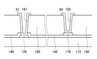
도 4는 도 3의 액정 표시 장치를 Ⅳ-Ⅳ 선을 따라 잘라 도시한 단면도이다.4 is a cross-sectional view of the liquid crystal display of FIG. 3 taken along the line IV-IV.
도 5는 도 3의 액정 표시 장치를 Ⅴ-Ⅴ 선을 따라 잘라 도시한 단면도이다.FIG. 5 is a cross-sectional view of the liquid crystal display of FIG. 3 taken along the line VV. FIG.
도 6은 본 발명의 다른 한 실시예에 따른 액정 표시 장치의 배치도이다.6 is a layout view of a liquid crystal display according to another exemplary embodiment of the present invention.
도 7은 도 6의 액정 표시 장치를 Ⅶ-Ⅶ 선을 따라 잘라 도시한 단면도이다.FIG. 7 is a cross-sectional view of the liquid crystal display of FIG. 6 taken along the line VII-VII. FIG.
도 8은 도 6의 액정 표시 장치를 Ⅷ-Ⅷ 선을 따라 잘라 도시한 단면도이다.FIG. 8 is a cross-sectional view of the liquid crystal display of FIG. 6 taken along the line VII-VII. FIG.
<도면 부호의 설명><Description of Drawing>
81, 82...접촉 보조 부재 81, 82 ... contact aid member
73, 74, 75a, 75b, 76a, 76b, 92, 93, 94a, 94b, 95a, 95b...절개부73, 74, 75a, 75b, 76a, 76b, 92, 93, 94a, 94b, 95a, 95b ...
100...박막 트랜지스터 표시판 110...기판Thin Film Transistor Display ...
121, 129...게이트선 124...게이트 전극121, 129 ...
131...유지 전극선 137...유지 전극131 Holding Electrode Wire 137 Holding Electrode
140...게이트 절연막 151, 154...반도체140 Gate
161, 163, 165...저항성 접촉층 171, 179...데이터선161, 163, 165 ...
173...소스 전극 175...드레인 전극173
177...유지 도전체 180...보호막177 Holding Conductor 180 Shield
181, 182, 185...접촉 구멍 191...화소 전극181, 182, 185
200...색필터 표시판 210...기판200 ...
220...차광 부재 230...색필터220 ... light-
250...덮개막 270...공통 전극250
본 발명은 액정 표시 장치에 관한 것으로서, 특히 절개부를 가지는 액정 표시 장치에 관한 것이다.The present invention relates to a liquid crystal display device, and more particularly, to a liquid crystal display device having a cutout.
액정 표시 장치는 현재 가장 널리 사용되고 있는 평판 표시 장치 중 하나로서, 화소 전극과 공통 전극 등 전기장 생성 전극이 형성되어 있는 두 장의 표시판과 그 사이에 들어 있는 액정층을 포함한다. 액정 표시 장치는 전기장 생성 전극에 전압을 인가하여 액정층에 전기장을 생성하고 이를 통하여 액정층의 액정 분자들의 방향을 결정하고 입사광의 편광을 제어함으로써 영상을 표시한다.The liquid crystal display is one of the most widely used flat panel display devices, and includes two display panels on which an electric field generating electrode such as a pixel electrode and a common electrode are formed, and a liquid crystal layer interposed therebetween. The liquid crystal display generates an electric field in the liquid crystal layer by applying a voltage to the field generating electrode, thereby determining an orientation of liquid crystal molecules of the liquid crystal layer and controlling the polarization of incident light to display an image.
액정 표시 장치 중에서도 전기장이 인가되지 않은 상태에서 액정 분자를 그 장축이 표시판에 대하여 수직을 이루도록 배열한 수직 배향 방식(vertically aligned mode) 액정 표시 장치는 대비비가 크고 기준 시야각이 넓어서 각광받고 있다.Among the liquid crystal display devices, a vertically aligned mode liquid crystal display in which liquid crystal molecules are arranged such that their long axes are perpendicular to the display panel without an electric field applied to the liquid crystal display device has a high contrast ratio and a wide reference viewing angle.
수직 배향 방식 액정 표시 장치에서 광시야각을 구현하기 위한 방법으로는 전기장 생성 전극에 절개부를 형성하는 방법과 전기장 생성 전극 위 또는 아래에 돌기를 형성하는 방법 등이 있다. 절개부 또는 돌기는 액정 분자가 기울어지는 방향을 결정해 주므로, 이들을 다양하게 배치하여 액정 분자의 경사 방향을 여러 방향으로 분산시킴으로써 기준 시야각을 넓힐 수 있다.Methods for implementing a wide viewing angle in a vertical alignment liquid crystal display include a method of forming a cutout in the field generating electrode and a method of forming protrusions on or under the field generating electrode. Since the incision or protrusion determines the direction in which the liquid crystal molecules are inclined, the reference viewing angle can be widened by disposing the variously arranged and dispersing the inclination directions of the liquid crystal molecules in various directions.
절개부를 형성하는 경우, 절개부의 면적이 넓을수록 액정 제어에 유리하지만 액정 표시 장치의 개구율은 저하된다.In the case where the cutout is formed, the larger the area of the cutout is, the more favorable the liquid crystal control is, but the aperture ratio of the liquid crystal display is lowered.
따라서, 본 발명이 이루고자 하는 기술적 과제는 액정 표시 장치의 액정을 잘 제어하면서도 액정 표시 장치의 개구율을 향상한 액정 표시 장치를 제공하는 것이다.Accordingly, an object of the present invention is to provide a liquid crystal display device in which the aperture ratio of the liquid crystal display device is improved while controlling the liquid crystal of the liquid crystal display device well.
본 발명의 한 특징에 따른 박막 트랜지스터 표시판은 기판, 상기 기판 위에 형성되어 있으며, 게이트 전극을 포함하는 게이트선 및 유지 전극을 포함하는 유지 전극선, 상기 기판 위에 형성되어 있는 게이트 절연막, 상기 게이트 절연막 위에 형성되어 있는 반도체층, 상기 게이트 절연막 및 상기 반도체층 위에 형성되어 있는 데이터선 및 드레인 전극, 상기 게이트 절연막 위에 상기 데이터선과 함께 형성되고, 상기 드레인 전극과 연결되어 있는 유지 도전체, 상기 데이터선, 드레인 전 극 및 유지 도전체 위에 형성되어 있는 보호막, 그리고 그리고 상기 보호막 위에 형성되어 있고, 상기 드레인 전극과 연결되어 있으며 복수의 절개부를 가지는 화소 전극을 포함하고, 상기 유지 전극 및 상기 유지 도전체는 상기 절개부와 중첩하는 사선부를 가지고, 상기 게이트 절연막을 사이에 두고 서로 중첩한다.A thin film transistor array panel according to an aspect of the present invention is formed on a substrate, a gate line including a gate electrode, and a storage electrode line including a storage electrode, a gate insulating film formed on the substrate, and a gate insulating film. A semiconductor layer, a data line and a drain electrode formed on the gate insulating film and the semiconductor layer, a storage conductor formed on the gate insulating film together with the data line and connected to the drain electrode, and the data line and the drain electrode. A protective film formed on the pole and the storage conductor, and a pixel electrode formed on the protective film and connected to the drain electrode and having a plurality of cutouts, wherein the storage electrode and the storage conductor are the cutouts. Has an oblique portion overlapping with the above The gate insulating film is interposed therebetween.
서로 중첩하는 상기 유지 전극의 폭과 상기 유지 도전체의 폭은 서로 같을 수 있다.The width of the storage electrode overlapping each other and the width of the storage conductor may be the same.
서로 중첩하는 상기 유지 전극의 폭과 상기 유지 도전체의 폭은 서로 다를 수 있다.The width of the storage electrode overlapping each other and the width of the storage conductor may be different from each other.
서로 중첩하는 상기 유지 전극의 폭은 상기 유지 도전체의 폭보다 클 수 있다.The width of the storage electrodes overlapping each other may be greater than the width of the storage conductor.
상기 유지 전극의 폭은 상기 유지 도전체의 폭보다 0.1㎛ 내지 10㎛ 클 수 있다.The width of the sustain electrode may be 0.1 μm to 10 μm greater than the width of the sustain conductor.
서로 중첩하는 상기 유지 도전체의 폭은 상기 유지 전극의 폭보다 클 수 있다.The width of the storage conductor overlapping each other may be greater than the width of the storage electrode.
상기 유지 도전체의 폭은 상기 유지 전극의 폭보다 0.1㎛ 내지 10㎛ 클 수 있다.The width of the storage conductor may be 0.1 μm to 10 μm greater than the width of the storage electrode.
본 발명의 실시예에 따른 액정 표시 장치는 제1 기판, 상기 제1 기판 위에 형성되어 있으며, 게이트 전극을 포함하는 게이트선 및 유지 전극을 포함하는 유지 전극선, 상기 기판 위에 형성되어 있는 게이트 절연막, 상기 게이트 절연막 위에 형성되어 있는 반도체층, 상기 게이트 절연막 및 상기 반도체층 위에 형성되어 있 는 데이터선 및 드레인 전극, 상기 게이트 절연막 위에 상기 데이터선과 함께 형성되고, 상기 드레인 전극과 연결되어 있는 유지 도전체, 상기 데이터선, 드레인 전극 및 유지 도전체 위에 형성되어 있는 보호막, 그리고 상기 보호막 위에 형성되어 있고, 상기 드레인 전극과 연결되어 있으며 제1 절개부를 가지는 화소 전극, 상기 제1 기판과 마주하는 제2 기판, 상기 제2 기판 위에 형성되어 있으며, 제2 절개부를 가지는 공통 전극, 그리고 상기 제1 기판과 상기 제2 기판 사이에 들어 있는 액정층을 포함하며, 상기 상기 유지 전극 및 상기 유지 도전체는 상기 절개부와 중첩하는 사선부를 가지고, 상기 게이트 절연막을 사이에 두고 서로 중첩한다.A liquid crystal display according to an exemplary embodiment of the present invention includes a first substrate, a gate line including a gate electrode, and a storage electrode line including a storage electrode, a gate insulating layer formed on the substrate, and A semiconductor layer formed over a gate insulating film, a data line and a drain electrode formed over the gate insulating film and the semiconductor layer, a storage conductor formed on the gate insulating film together with the data line, and connected to the drain electrode; A protective film formed on the data line, the drain electrode and the storage conductor, and a pixel electrode formed on the protective film and connected to the drain electrode and having a first cutout, a second substrate facing the first substrate, and A common electrode formed on the second substrate and having a second cutout; Includes the first liquid crystal layer that contains between the first substrate and the second substrate, wherein the sustain electrode and the sustain conductors across the with unit diagonal which overlaps with the cutting portion, wherein the gate insulating film overlaps each other.
상기 액정층의 유절율(ε), 상기 액정층 두께(d), 상기 보호막의 유전율(ε'), 그리고 상기 보호막의 두께(d')는 εd'/ε'd>0.1을 만족할 수 있다.The dielectric constant (ε) of the liquid crystal layer, the liquid crystal layer thickness (d), the dielectric constant (ε ') of the protective film, and the thickness (d') of the protective film may satisfy εd '/ ε'd> 0.1.
서로 중첩하는 상기 유지 전극의 폭과 상기 유지 도전체의 폭은 서로 같을 수 있다.The width of the storage electrode overlapping each other and the width of the storage conductor may be the same.
서로 중첩하는 상기 유지 전극의 폭과 상기 유지 도전체의 폭은 서로 다를 수 있다.The width of the storage electrode overlapping each other and the width of the storage conductor may be different from each other.
상기 유지 전극의 폭은 상기 유지 도전체의 폭보다 0.1㎛ 내지 10㎛ 클 수 있다.The width of the sustain electrode may be 0.1 μm to 10 μm greater than the width of the sustain conductor.
상기 유지 도전체의 폭은 상기 유지 전극의 폭보다 0.1㎛ 내지 10㎛ 클 수 있다.The width of the storage conductor may be 0.1 μm to 10 μm greater than the width of the storage electrode.
상기 제2 절개부는 상기 제1 절개부와 교대로 배치되어 있을 수 있다.The second cutout may be alternately arranged with the first cutout.
상기 액정 표시 장치는 상기 제2 기판 위에 형성되어 있는 차광 부재, 그리 고 상기 제2 기판 및 상기 차광 부재 위에 형성되어 있는 색필터를 더 포함할 수 있다.The liquid crystal display may further include a light blocking member formed on the second substrate, and a color filter formed on the second substrate and the light blocking member.
첨부한 도면을 참고로 하여 본 발명의 실시예에 대하여 본 발명이 속하는 기술 분야에서 통상의 지식을 가진 자가 용이하게 실시할 수 있도록 상세히 설명한다. 그러나 본 발명은 여러 가지 상이한 형태로 구현될 수 있으며 여기에서 설명하는 실시예에 한정되지 않는다.DETAILED DESCRIPTION Embodiments of the present invention will be described in detail with reference to the accompanying drawings so that those skilled in the art may easily implement the present invention. As those skilled in the art would realize, the described embodiments may be modified in various different ways, all without departing from the spirit or scope of the present invention.
도면에서 여러 층 및 영역을 명확하게 표현하기 위하여 두께를 확대하여 나타내었다. 명세서 전체를 통하여 유사한 부분에 대해서는 동일한 도면 부호를 붙였다. 층, 막, 영역, 판 등의 부분이 다른 부분 "위에" 있다고 할 때, 이는 다른 부분 "바로 위에" 있는 경우뿐 아니라 그 중간에 또 다른 부분이 있는 경우도 포함한다. 반대로 어떤 부분이 다른 부분 "바로 위에" 있다고 할 때에는 중간에 다른 부분이 없는 것을 뜻한다.In the drawings, the thickness of layers, films, panels, regions, etc., are exaggerated for clarity. Like parts are designated by like reference numerals throughout the specification. When a part of a layer, film, region, plate, etc. is said to be "on" another part, this includes not only the other part being "right over" but also another part in the middle. On the contrary, when a part is "just above" another part, there is no other part in the middle.
그러면 도 1 내지 도 3을 참고로 하여 본 발명의 한 실시예에 따른 박막 트랜지스터 표시판 및 이를 포함한 액정 표시 장치에 대하여 상세하게 설명한다. 도 1은 본 발명의 한 실시예에 따른 액정 표시 장치용 박막 트랜지스터 표시판의 배치도이고, 도 2는 도 1의 박막 트랜지스터 표시판을 Ⅱ-Ⅱ 선을 따라 잘라 도시한 단면도이고, 도 3은 도 1의 박막 트랜지스터 표시판을 Ⅲ-Ⅲ 선을 따라 잘라 도시한 단면도이다.Next, a thin film transistor array panel and a liquid crystal display including the same according to an exemplary embodiment of the present invention will be described in detail with reference to FIGS. 1 to 3. 1 is a layout view of a thin film transistor array panel for a liquid crystal display according to an exemplary embodiment of the present invention. FIG. 2 is a cross-sectional view of the thin film transistor array panel of FIG. 1 taken along a line II-II. FIG. 3 is a cross-sectional view of FIG. The thin film transistor array panel is cut along the III-III line.
본 실시예에 따른 액정 표시 장치는 박막 트랜지스터 표시판(100), 공통 전극 표시판(200), 그리고 이들 두 표시판(100, 200) 사이에 들어 있는 액정층(3)을 포함한다.The liquid crystal display according to the present exemplary embodiment includes a thin film
먼저, 도 1, 도 3을 참고로 하여 박막 트랜지스터 표시판에 대하여 설명한다.First, a thin film transistor array panel will be described with reference to FIGS. 1 and 3.
투명한 유리 또는 플라스틱 따위로 만들어진 절연 기판(110) 위에 복수의 게이트선(gate line)(121) 및 복수의 유지 전극선(storage electrode line)(131)이 형성되어 있다.A plurality of
게이트선(121)은 게이트 신호를 전달하며 주로 가로 방향으로 뻗어 있다. 각 게이트선(121)은 위로 돌출한 복수의 게이트 전극(gate electrode)(124)과 다른 층 또는 외부 구동 회로와의 접속을 위한 넓은 끝 부분(129)을 포함한다. 게이트 신호를 생성하는 게이트 구동 회로(도시하지 않음)는 기판(110) 위에 부착되는 가요성 인쇄 회로막(flexible printed circuit film)(도시하지 않음) 위에 장착되거나, 기판(110) 위에 직접 장착되거나, 기판(110)에 집적될 수 있다. 게이트 구동 회로가 기판(110) 위에 집적되어 있는 경우 게이트선(121)이 연장되어 이와 직접 연결될 수 있다.The
유지 전극선(131)은 소정의 전압을 인가 받으며, 게이트선(121)과 거의 나란하게 뻗는다. 각 유지 전극선(131)은 인접한 두 게이트선(121) 사이에 위치하며 두 게이트선(121)과 거의 동일한 거리를 두고 있다. 유지 전극선(131)은 아래위로 확장된 유지 전극(storage electrode)(137)을 포함하는데, 유지 전극(137)은 유지 전극선(131)이 위아래도 돌출한 형태의 가로부(137c), 가로부(137c)로부터 상하 사선 방향으로 각각 뻗어 나간 제1 사선부(137d) 및 제2 사선부(137e), 가로부(137c) 의 오른쪽으로부터 세로 방향으로 뻗은 수직부(137b), 수직부(137d)로부터 왼쪽 방향으로 사선으로 뻗은 제1 사선부(137a)를 포함한다. 그러나 유지 전극선(131)의 모양 및 배치는 여러 가지로 변형될 수 있다.The
게이트선(121) 및 유지 전극선(131)은 알루미늄(Al)이나 알루미늄 합금 등 알루미늄 계열 금속, 은(Ag)이나 은 합금 등 은 계열 금속, 구리(Cu)나 구리 합금 등 구리 계열 금속, 몰리브덴(Mo)이나 몰리브덴 합금 등 몰리브덴 계열 금속, 크롬(Cr), 탄탈륨(Ta) 및 티타늄(Ti) 따위로 만들어질 수 있다. 그러나 이들은 물리적 성질이 다른 두 개의 도전막(도시하지 않음)을 포함하는 다중막 구조를 가질 수도 있다. 이 중 한 도전막은 신호 지연이나 전압 강하를 줄일 수 있도록 비저항(resistivity)이 낮은 금속, 예를 들면 알루미늄 계열 금속, 은 계열 금속, 구리 계열 금속 등으로 만들어진다. 이와는 달리, 다른 도전막은 다른 물질, 특히 ITO(indium tin oxide) 및 IZO(indium zinc oxide)와의 물리적, 화학적, 전기적 접촉 특성이 우수한 물질, 이를테면 몰리브덴 계열 금속, 크롬, 탄탈륨, 티타늄 등으로 만들어진다. 이러한 조합의 좋은 예로는 크롬 하부막과 알루미늄 (합금) 상부막 및 알루미늄 (합금) 하부막과 몰리브덴 (합금) 상부막을 들 수 있다. 그러나 게이트선(121) 및 유지 전극선(131)은 이외에도 여러 가지 다양한 금속 또는 도전체로 만들어질 수 있다.The
게이트선(121) 및 유지 전극선(131)의 측면은 기판(110) 면에 대하여 경사져 있으며 그 경사각은 약 30° 내지 약 80°인 것이 바람직하다.Side surfaces of the
게이트선(121) 및 유지 전극선(131) 위에는 질화규소(SiNx) 또는 산화규소(SiOx) 따위로 만들어진 게이트 절연막(gate insulating layer)(140)이 형성되어 있다.A
게이트 절연막(140) 위에는 수소화 비정질 규소(hydrogenated amorphous silicon)(비정질 규소는 약칭 a-Si로 씀) 또는 다결정 규소(polysilicon) 등으로 만들어진 복수의 선형 반도체(151)가 형성되어 있다. 선형 반도체(151)는 주로 세로 방향으로 뻗으며, 게이트 전극(124)을 향하여 뻗어 나온 복수의 돌출부(projection)(154)를 포함한다. 선형 반도체(151)는 게이트선(121) 및 유지 전극선(131) 부근에서 너비가 넓어져 이들을 폭넓게 덮고 있다.A plurality of
반도체(151) 위에는 복수의 선형 및 섬형 저항성 접촉 부재(ohmic contact)(161, 165)가 형성되어 있다. 저항성 접촉 부재(161, 165)는 인 따위의 n형 불순물이 고농도로 도핑되어 있는 n+ 수소화 비정질 규소 따위의 물질로 만들어지거나 실리사이드(silicide)로 만들어질 수 있다. 선형 저항성 접촉 부재(161)는 복수의 돌출부(163)를 가지고 있으며, 이 돌출부(163)와 섬형 저항성 접촉 부재(165)는 쌍을 이루어 반도체(151)의 돌출부(154) 위에 배치되어 있다.A plurality of linear and island ohmic
반도체(151)와 저항성 접촉 부재(161, 165)의 측면 역시 기판(110) 면에 대하여 경사져 있으며 그 경사각은 30° 내지 80° 정도인 것이 바람직하다.Side surfaces of the
저항성 접촉 부재(161, 165) 및 게이트 절연막(140) 위에는 복수의 데이터선(data line)(171)과 복수의 드레인 전극(drain electrode)(175) 및 복수의 유지 도 전체(storage conductor)(177)가 형성되어 있다.A plurality of
데이터선(171)은 데이터 전압을 전달하며 주로 세로 방향으로 뻗어 게이트선(121)과 교차한다. 각 데이터선은 게이트 전극(124)을 향하여 뻗은 복수의 소스 전극(source electrode)(173)과 다른 층 또는 외부 구동 회로와의 접속을 위한 넓은 끝 부분(179)을 포함한다. 데이터 전압을 생성하는 데이터 구동 회로(도시하지 않음)는 기판(110) 위에 부착되는 가요성 인쇄 회로막(도시하지 않음) 위에 장착되거나, 기판(110) 위에 직접 장착되거나, 기판(110)에 집적될 수 있다. 데이터 구동 회로가 기판(110) 위에 집적되어 있는 경우, 데이터선(171)이 연장되어 이와 직접 연결될 수 있다.The
드레인 전극(175)은 데이터선(171)과 분리되어 있으며 게이트 전극(124)을 중심으로 소스 전극(173)과 마주 본다. 각 드레인 전극(175)은 막대형인 한쪽 끝 부분과 유지 도전체(177)를 가지고 있으며, 막대형 끝 부분은 U자형으로 구부러진 소스 전극(173)으로 일부 둘러싸여 있다.The
하나의 게이트 전극(124), 하나의 소스 전극(173) 및 하나의 드레인 전극(175)은 반도체(151)의 돌출부(154)와 함께 하나의 박막 트랜지스터(thin film transistor, TFT)를 이루며, 박막 트랜지스터의 채널(channel)은 소스 전극(173)과 드레인 전극(175) 사이의 돌출부(154)에 형성된다.One
유지 도전체(177)는 드레인 전극(175)의 소스 전극(173)으로 둘러싸여 있는 막대형 끝 부분으로부터 연장되어 사선 방향으로 뻗은 제1 사선부(177a), 제1 사선부(177a)로부터 연장되어 세로 방향으로 뻗은 수직부(177b), 수직부(177b)로부터 연장되어 가로 방향으로 뻗은 가로부(177c), 가로부(177c)로부터 상하 사선 방향으로 각각 뻗어 나간 제2 사선부(177d) 및 제3 사선부(177e)를 포함한다. 이러한 유지 도전체(177)의 각 부분은 유지 전극(137)의 각 부분과 중첩한다. 본 실시예에 따른 박막 트랜지스터 표시판의 유지 도전체(177)의 폭은 유지 전극(137)의 폭보다 좁거나 같을 수 있고, 유지 전극(137)의 폭은 유지 도전체(177)의 폭보다 약 0㎛ 내지 약 10㎛ 정도 넓을 수 있다.The
데이터선(171)과 드레인 전극(175) 및 유지 도전체(177)는 몰리브덴, 크롬, 탄탈륨 및 티타늄 등 내화성 금속(refractory metal) 또는 이들의 합금으로 만들어지는 것이 바람직하며, 내화성 금속막(도시하지 않음)과 저저항 도전막(도시하지 않음)을 포함하는 다중막 구조를 가질 수 있다. 다중막 구조의 예로는 크롬 또는 몰리브덴 (합금) 하부막과 알루미늄 (합금) 상부막의 이중막, 몰리브덴 (합금) 하부막과 알루미늄 (합금) 중간막과 몰리브덴 (합금) 상부막의 삼중막을 들 수 있다. 그러나 데이터선(171)과 드레인 전극(175) 및 유지 도전체(177)는 이외에도 여러 가지 다양한 금속 또는 도전체로 만들어질 수 있다.The
데이터선(171)과 드레인 전극(175) 및 유지 도전체(177) 또한 그 측면이 기판(110) 면에 대하여 30° 내지 80° 정도의 경사각으로 기울어진 것이 바람직하다.The
저항성 접촉 부재(161, 165)는 그 아래의 반도체(151)와 그 위의 데이터선(171) 및 드레인 전극(175) 사이에만 존재하며 접촉 저항을 낮추어 준다. 대부분의 곳에서는 선형 반도체(151)가 데이터선(171)보다 좁지만, 앞서 설명하였듯이 게 이트선(121) 및 유지 전극선(131)과 만나는 부분에서 너비가 넓어져 표면의 프로파일을 부드럽게 함으로써 데이터선(171)이 단선되는 것을 방지한다. 반도체(151)는 소스 전극(173)과 드레인 전극(175) 사이를 비롯하여 데이터선(171) 및 드레인 전극(175)에 가리지 않고 노출된 부분을 가지고 있다.The
데이터선(171), 드레인 전극(175), 유지 도전체(177) 및 노출된 반도체(151) 부분 위에는 보호막(passivation layer)(180)이 형성되어 있다. 보호막(180)은 무기 절연물 또는 유기 절연물 따위로 만들어지며 표면이 평탄할 수 있다. 무기 절연물의 예로는 질화규소와 산화규소를 들 수 있다. 유기 절연물은 감광성(photosensitivity)을 가질 수 있으며 그 유전 상수(dielectric constant)는 약 4.0 이하인 것이 바람직하다. 그러나 보호막(180)은 유기막의 우수한 절연 특성을 살리면서도 노출된 반도체(151) 부분에 해가 가지 않도록 하부 무기막과 상부 유기막의 이중막 구조를 가질 수 있다.A
보호막(180)에는 데이터선(171)의 끝 부분(179)과 드레인 전극(175)을 각각 드러내는 복수의 접촉 구멍(contact hole)(182, 185)이 형성되어 있으며, 보호막(180)과 게이트 절연막(140)에는 게이트선(121)의 끝 부분(129)을 드러내는 복수의 접촉 구멍(181)이 형성되어 있다.In the
보호막(180) 위에는 복수의 화소 전극(pixel electrode)(191) 및 복수의 접촉 보조 부재(contact assistant)(81, 82)가 형성되어 있다. 이들은 ITO 또는 IZO 등의 투명한 도전 물질이나 알루미늄, 은, 크롬 또는 그 합금 등의 반사성 금속으로 만들어질 수 있다.A plurality of
화소 전극(191)은 접촉 구멍(185)을 통하여 드레인 전극(175)과 물리적ㅇ전기적으로 연결되어 있으며, 드레인 전극(175)으로부터 데이터 전압을 인가 받는다. 데이터 전압이 인가된 화소 전극(191)은 공통 전압(common voltage)을 인가 받는 공통 전극 표시판(200)의 공통 전극(common electrode)(270)과 함께 전기장을 생성함으로써 두 전극 사이의 액정층(3)의 액정 분자(도시하지 않음)의 방향을 결정한다. 이와 같이 결정된 액정 분자의 방향에 따라 액정층을 통과하는 빛의 편광이 달라진다. 화소 전극(191)과 공통 전극(270)은 축전기[이하 "액정 축전기(liquid crystal capacitor)"라 함]를 이루어 박막 트랜지스터가 턴 오프된 후에도 인가된 전압을 유지한다.The
앞서 설명하였듯이, 유지 도전체(177)는 유지 전극(137)을 비롯한 유지 전극선(131)과 중첩한다. 화소 전극(191)과 전기적으로 연결된 유지 도전체(177)가 유지 전극선(131)과 중첩하여 이루는 축전기를 "유지 축전기(storage capacitor)"라 하며, 유지 축전기는 액정 축전기의 전압 유지 능력을 강화한다. 본 발명의 실시예에 따른 액정 표시 장치의 박막 트랜지스터 표시판에서 서로 중첩하여 유지 축전기를 이루는 유지 전극(137)과 유지 도전체(177)는 화소 전극의 절개부(92-95b) 아래에 배치되어 있는 사선부(137a, 137d, 137e, 177a, 177d, 177e)를 가지는데, 이러한 사선부(137a, 137d, 137e, 177a, 177d, 177e)의 폭은 화소 전극의 절개부(92-95b)의 폭과 같은 것이 바람직하다.As described above, the
각 화소 전극(191)은 게이트선(121) 또는 데이터선(171)과 거의 평행한 네 개의 주 변을 가지며 모퉁이가 모따기되어 있는(chamfered) 대략 사각형 모양이다. 화소 전극(191)의 모딴 빗변은 게이트선(121)에 대하여 약 45°의 각도를 이룬다.Each
화소 전극(191)에는 중앙 절개부(92, 93), 하부 절개부(94a, 95a) 및 상부 절개부(94b, 95b)가 형성되어 있으며, 화소 전극(191)은 이들 절개부(92-95b)에 의하여 복수의 영역(partition)으로 분할된다. 절개부(92-95b)는 화소 전극(191)을 이등분하는 가상의 가로 중심선에 대하여 거의 반전 대칭을 이룬다.The
하부 및 상부 절개부(94a-95b)는 대략 화소 전극(191)의 왼쪽 변, 위쪽 변에서부터 오른쪽 변으로 비스듬하게 뻗어 있으며, 화소 전극(191)의 가로 중심선에 대하여 하반부와 상반부에 각각 위치하고 있다. 하부 및 상부 절개부(94a-95b)는 게이트선(121)에 대하여 약 45°의 각도를 이루며 서로 수직하게 뻗어 있다.The lower and
중앙 절개부(92)는 화소 전극(191)의 중앙에 배치되어 있으며, 왼쪽 변에 위치한 입구를 가지고 있다. 중앙 절개부(92)의 입구는 하부 절개부(94a, 95a)와 상부 절개부(94b, 95b)에 각각 거의 평행한 한 쌍의 빗변을 가지고 있다. 중앙 절개부(93)는 화소 전극(191)의 가로 중심선으로부터 화소 전극(191)의 왼쪽 변으로 비스듬하게 뻗은 한 쌍의 사선부를 가진다. The
따라서 화소 전극(191)의 하반부는 중앙 절개부(93) 및 하부 절개부(94a, 95a)에 의하여 네 개의 영역(partition)으로 나누어지고, 상반부 또한 중앙 절개부(93) 및 상부 절개부(94b, 95b)에 의하여 네 개의 영역으로 분할된다. 이 때, 영역의 수효 또는 절개부의 수효는 화소 전극(191)의 크기, 화소 전극(191)의 가로변과 세로 변의 길이 비, 액정층(3)의 종류나 특성 등 설계 요소에 따라서 달라질 수 있다.Therefore, the lower half of the
절개부(92-95b) 중 중앙 절개부(93)와 하부 절개부(94a)는 유지 도전체(177)의 제1 내지 제3 사선부(177a, 177d, 177e) 및 유지 전극(137)의 사선부()와 중첩한다. The
이와 같이, 개구율을 저하시키는 유지 전극(137) 및 유지 도전체(177)를 역시 개구율을 저하시키는 절개부(92-95b)와 중첩하도록 형성하면 액정 표시 장치의 개구율을 향상할 수 있다.As described above, when the sustain
접촉 보조 부재(81, 82)는 각각 접촉 구멍(181, 182)을 통하여 게이트선(121)의 끝 부분(129) 및 데이터선(171)의 끝 부분(179)과 연결된다. 접촉 보조 부재(81, 82)는 게이트선(121)의 끝 부분(129) 및 데이터선(171)의 끝 부분(179)과 외부 장치와의 접착성을 보완하고 이들을 보호한다.The contact
한편, 본 발명의 실시예에 따른 액정 표시 장치에서, 액정의 유절율이 ε이고, 액정 표시 장치의 셀 간격이 d이고, 보호막(180)의 유전율이 ε'이고, 보호막(180)의 두께가 d'인 경우, εd'/ε'd>0.1을 만족하는 것이 바람직하다.On the other hand, in the liquid crystal display according to the embodiment of the present invention, the dielectric constant of the liquid crystal is ε, the cell gap of the liquid crystal display is d, the dielectric constant of the
다음으로, 도 2 내지 도 4를 참고로 하여, 공통 전극 표시판(200)에 대하여 설명한다. Next, the common
투명한 유리 또는 플라스틱 등으로 만들어진 절연 기판(210) 위에 차광 부재(light blocking member)(220)가 형성되어 있다. 차광 부재(220)는 블랙 매트릭스(black matrix)라고도 하며 빛샘을 막아준다. 차광 부재(220)는 화소 전극(191)과 마주보며 화소 전극(191)과 거의 동일한 모양을 가지는 복수의 개구부(225)를 가지고 있으며, 화소 전극(191) 사이의 빛샘을 막는다. 그러나 차광 부재(22)는 게이 트선(121) 및 데이터선(171)에 대응하는 부분과 박막 트랜지스터에 대응하는 부분으로 이루어질 수 있다.A
기판(210) 위에는 또한 복수의 색필터(230)가 형성되어 있다. 색필터(230)는 차광 부재(230)로 둘러싸인 영역 내에 대부분 존재하며, 화소 전극(191) 열을 따라서 세로 방향으로 길게 뻗을 수 있다. 각 색필터(230)는 적색, 녹색 및 청색의 삼원색 등 기본색(primary color) 중 하나를 표시할 수 있다.A plurality of
색필터(230) 및 차광 부재(220) 위에는 덮개막(overcoat)(250)이 형성되어 있다. 덮개막(250)은 (유기) 절연물로 만들어질 수 있으며, 색필터(230)가 노출되는 것을 방지하고 평탄면을 제공한다. An
덮개막(250) 위에는 ITO, IZO 등의 투명한 도전체 따위로 이루어진 공통 전극(270)이 형성되어 있다. The
공통 전극(270)은 복수의 절개부(73, 74, 75a, 75b, 76a, 76b) 집합을 가진다.The
하나의 절개부(73-75b) 집합은 하나의 화소 전극(191)과 마주하며 중앙 절개부(73, 74), 하부 절개부(75a, 76a) 및 상부 절개부(75b. 76b)를 포함한다. 절개부(73-75b) 각각은 화소 전극(191)의 인접 절개부(92-95b) 사이 또는 절개부(94a-95b)와 화소 전극(191)의 모딴 빗변 사이에 배치되어 있다. 또한, 각 절개부(73-75b 는 화소 전극(191)의 하부 절개부(94a, 95a) 또는 상부 절개부(94b, 95b)와 평행하게 뻗은 적어도 하나의 사선부를 포함하며, 각 사선부에는 움푹 팬 노치(notch)를 포함할 수 있다. 공통 전극(270) 절개부(73-75b)의 노치는 절개부(73- 75b) 위에 위치한 액정 분자들의 경사 방향을 결정한다. 노치는 화소 전극(191)의 절개부(92-95b)에도 형성될 수 있고, 생략될 수도 있다.One set of cutouts 73-75b faces a
하부 및 상부 절개부(75a, 75b, 76a, 76b) 각각은 사선부와 가로부 및 세로부를 포함한다. 사선부는 대략 화소 전극(191)의 위쪽 또는 아래쪽 변에서 오른쪽 변으로 뻗는다. 가로부 및 세로부는 사선부의 각 끝에서부터 화소 전극(191)의 변을 따라 변과 중첩하면서 뻗으며 사선부와 둔각을 이룬다.Each of the lower and
중앙 절개부(73, 74)는 중앙 가로부, 한 쌍의 사선부 및 한 쌍의 종단 세로부를 포함한다. 중앙 가로부는 대략 화소 전극(191)의 오른쪽 변 또는 중앙에서부터 화소 전극(191)의 가로 중심선을 따라 왼쪽으로 뻗으며, 한 쌍의 사선부는 중앙 가로부의 끝에서부터 화소 전극(191)의 왼쪽 변을 향하여 각각 하부 및 상부 절개부(75a, 75b)와 거의 나란하게 뻗는다. 종단 세로부는 해당 사선부의 끝에서부터 화소 전극(191)의 오른쪽 변을 따라 오른쪽 변과 중첩하면서 뻗으며 사선부와 둔각을 이룬다.The
절개부(73-75b)의 수효 또한 설계 요소에 따라 달라질 수 있으며, 차광 부재(220)가 절개부(73-75b)와 중첩하여 절개부(73-75b) 부근의 빛샘을 차단할 수 있다.The number of cutouts 73-75b may also vary according to design factors, and the
표시판(100, 200)의 안쪽 면에는 배향막(alignment layer)(11, 21)이 도포되어 있으며, 이들은 수직 배향막일 수 있다. 표시판(100, 200)의 바깥쪽 면에는 편광자(polarizer)(도시하지 않음)가 구비되어 있을 수 있는데, 두 편광자의 편광축은 직교하며 이중 한 편광축은 게이트선(121)에 대하여 나란한 것이 바람직하다. 반사형 액정 표시 장치의 경우에는 두 개의 편광자 중 하나가 생략될 수 있다.Alignment layers 11 and 21 are coated on inner surfaces of the
본 실시예에 따른 액정 표시 장치는 액정층의 지연을 보상하기 위한 위상 지연막(retardation film)(도시하지 않음)을 더 포함할 수 있다. 액정 표시 장치는 또한 편광자, 위상 지연막, 표시판(100, 200) 및 액정층(3)에 빛을 공급하는 조명부(backlight unit)(도시하지 않음)를 포함할 수 있다.The liquid crystal display according to the present exemplary embodiment may further include a phase retardation film (not shown) for compensating for the delay of the liquid crystal layer. The liquid crystal display may also include a polarizer, a phase retardation film,
액정층(3)은 음의 유전율 이방성을 가지며, 액정층(3)의 액정 분자는 전기장이 없는 상태에서 그 장축이 두 표시판(100, 200)의 표면에 대하여 수직을 이루도록 배향되어 있다. 따라서 입사광은 직교 편광자를 통과하지 못하고 차단된다.The
공통 전극(270)에 공통 전압을 인가하고 화소 전극(191)에 데이터 전압을 인가하면 표시판(100, 200)의 표면에 거의 수직인 전기장(전계)이 생성된다. 액정 분자들은 전기장에 응답하여 그 장축이 전기장의 방향에 수직을 이루도록 방향을 바꾸고자 한다. 앞으로는 화소 전극(191)과 공통 전극(270)을 통틀어 전기장 생성 전극이라 한다.When a common voltage is applied to the
전기장 생성 전극(191, 270)의 절개부(73-75b, 92-95b)와 화소 전극(191)의 변은 전기장을 왜곡하여 액정 분자들의 경사 방향을 결정하는 수평 성분을 만들어낸다. 전기장의 수평 성분은 절개부(73-75b, 92-95b)의 변과 화소 전극(191)의 변에 거의 수직이다.The cutouts 73-75b and 92-95b of the
도 3을 참고하면, 하나의 절개부 집합(73-75b, 92-95b)은 화소 전극(191)을 복수의 부영역(sub-area)으로 나누며, 각 부영역은 화소 전극(191)의 주 변과 빗각을 이루는 두 개의 주 변(major edge)을 가진다. 각 부영역 위의 액정 분자들은 대부분 주 변에 수직인 방향으로 기울어지므로, 기울어지는 방향을 추려보면 대략 네 방향이다. 이와 같이 액정 분자가 기울어지는 방향을 다양하게 하면 액정 표시 장치의 기준 시야각이 커진다.Referring to FIG. 3, one set of cutouts 73-75b and 92-95b divides the
적어도 하나의 절개부(73-75b, 92-95b)는 돌기(protrusion)(도시하지 않음)나 함몰부(depression)(도시하지 않음)로 대체할 수 있다. 돌기는 유기물 또는 무기물로 만들어질 수 있고 전기장 생성 전극(191, 270)의 위 또는 아래에 배치될 수 있다.At least one incision 73-75b, 92-95b may be replaced with a protrusion (not shown) or depression (not shown). The protrusions may be made of organic or inorganic materials and may be disposed above or below the
한편, 본 발명의 실시예에 따른 박막 트랜지스터 표시판의 화소 전극(191)의 절개부 집합(92-95b) 중 일부 아래에는 화소 전극과 동일한 전압이 인가되는 유지 도전체(177)가 배치되어 있다. 이처럼 화소 전극(191)의 절개부 집합(92-95b) 아래에 전압이 인가되는 유지 도전체(177)가 배치되어 있는 경우, 화소 전극(191)의 절개부 집합(92-95b)이 액정 분자들의 기울어지는 방향을 제어할 수 있는 정도의 크기를 가지는 전기장의 수평 성분을 만들기 위하여 다음의 관계를 만족해야 한다.On the other hand, a sustain
VSC<VP(1+εd'/ε'd)V SC <V P (1 + εd '/ ε'd)
여기서, VSC는 유지 도전체(177)에 인가되는 전압이고, VP는 화소 전극(191)에 인가되는 전압이고, ε과 d는 액정의 유전율 및 셀 간격이고, ε' 및 d'은 보호막(180)의 유전율 및 두께이다.Here, V SC is a voltage applied to the
본 발명의 실시예에 따른 박막 트랜지스터 표시판의 경우, 유지 도전체(177)와 화소 전극(191)에는 동일한 데이터 전압이 인가되므로, VSC와 VP는 같고, εd'/ ε'd>0.1 이므로, 위의 식을 만족한다.In the case of the thin film transistor array panel according to the exemplary embodiment of the present invention, since the same data voltage is applied to the
따라서, 본 발명의 실시예에 따른 액정 표시 장치의 박막 트랜지스터 표시판은 화소 전극(191)의 절개부(92-95b) 아래에 절개부(92-95b)와 폭이 같은 사선부를 가지는 유지 전극(137) 및 유지 도전체(177)를 배치함으로써, 유지 전극(137) 및 유지 도전체(177)가 화소 전극(191)의 절개부(92-95b) 아래에 배치되어 있지 않은 일반적인 액정 표시 장치와 비교하여 액정 표시 장치의 개구율은 증가하면서, 화소 전극(191)이 가지는 절개부(92-95b) 집합이 액정 분자들의 기울어지는 방향을 제어할 수 있는 정도의 크기를 가지는 전기장의 수평 성분을 만들 수 있다.Therefore, the thin film transistor array panel of the liquid crystal display according to the exemplary embodiment of the present invention has a sustain
그러면 도 6 내지 도 8을 참고하여 본 발명의 다른 실시예에 따른 액정 표시 장치에 대하여 상세하게 설명한다. 도 6은 본 발명의 다른 한 실시예에 따른 액정 표시 장치의 배치도이고, 도 7은 도 6의 액정 표시 장치를 Ⅶ-Ⅶ 선을 따라 잘라 도시한 단면도이고, 도 8은 도 6의 액정 표시 장치를 Ⅷ-Ⅷ 선을 따라 잘라 도시한 단면도이다.Next, a liquid crystal display according to another exemplary embodiment of the present invention will be described in detail with reference to FIGS. 6 to 8. FIG. 6 is a layout view of a liquid crystal display according to another exemplary embodiment. FIG. 7 is a cross-sectional view of the liquid crystal display of FIG. 6 taken along the line VII-VII. FIG. 8 is a liquid crystal display of FIG. 6. Is a cross-sectional view taken along the line Ⅷ-Ⅷ.
본 실시예에 따른 액정 표시 장치도 박막 트랜지스터 표시판(100), 공통 전극 표시판(200) 및 이들 두 표시판(100, 200) 사이에 들어 있는 액정층(3)을 포함한다.The liquid crystal display according to the present exemplary embodiment also includes a thin film
본 실시예에 따른 표시판(100, 200)의 층상 구조는 도 1 내지 도 5와 거의 동일하다.The layered structure of the
박막 트랜지스터 표시판(100)에 대하여 설명하자면, 기판(110) 위에 게이트 전극(124)을 포함하는 복수의 게이트선(121), 유지 전극(137)을 포함하는 복수의 유지 전극선(131)이 형성되어 있고, 그 위에 게이트 절연막(140), 돌출부(154)를 포함하는 복수의 선형 반도체(151), 돌출부(163)를 포함하는 복수의 선형 저항성 접촉 부재(161) 및 복수의 섬형 저항성 접촉 부재(165)가 차례로 형성되어 있다. 저항성 접촉 부재(161, 165) 위에는 소스 전극(173)을 포함하는 복수의 데이터선(171), 복수의 드레인 전극(175)이 형성되어 있고, 데이터선(171)과 동일한 층으로 함께 형성되고 드레인 전극(175)과 연결되어 있는 유지 도전체(177)가 형성되어 있고, 그 위에 보호막(180)이 형성되어 있다. 보호막(180) 및 게이트 절연막(140)에는 복수의 접촉 구멍(181, 182, 185)이 형성되어 있으며, 그 위에는 복수의 화소 전극(191), 복수의 접촉 보조 부재(81, 82) 및 배향막(11)이 형성되어 있다.Referring to the thin film
공통 전극 표시판(200)에 대하여 설명하자면, 차광 부재(220), 복수의 색필터(230), 공통 전극(270) 및 배향막(21)이 절연 기판(210) 위에 형성되어 있다.To describe the common
그러나 도 1 내지 도 5에 도시한 액정 표시 장치와 달리, 유지 전극(137)의 폭은 도전체(177)의 폭보다 좁거나 같을 수 있고, 유지 도전체(177)의 폭은 유지 전극(137)의 폭보다 약 0㎛ 내지 약 10㎛ 정도 넓을 수 있다.However, unlike the liquid crystal display shown in FIGS. 1 to 5, the width of the
본 실시예에 따른 액정 표시 장치의 유지 전극(137) 및 유지 도전체(177) 역시 절개부(92-95b)와 중첩하는 사선부를 가지고, 액정의 유절율이 ε이고, 액정 표시 장치의 셀 간격이 d이고, 보호막(180)의 유전율이 ε'이고, 보호막(180)의 두께가 d'인 경우, εd'/ε'd>0.1을 만족한다.The sustain
따라서, 본 발명의 실시예에 따른 액정 표시 장치의 박막 트랜지스터 표시판의 유지 전극(137) 및 유지 도전체(177)는 화소 전극(191)의 절개부(92-95b)와 중 첩하는 사선부를 가짐으로써, 유지 전극(137) 및 유지 도전체(177)가 화소 전극(191)의 절개부(92-95b) 아래에 배치되어 있는 사선부를 가지지 않은 일반적인 액정 표시 장치와 비교하여 액정 표시 장치의 개구율은 증가하면서, 화소 전극(191)이 가지는 절개부(92-95b) 집합이 액정 분자들의 기울어지는 방향을 제어할 수 있는 정도의 크기를 가지는 전기장의 수평 성분을 만들 수 있다.Therefore, the sustain
이상과 같이, 본 발명에서는 본 실시예에 따른 액정 표시 장치의 박막 트랜지스터 표시판은 화소 전극의 절개부와 중첩하는 사선부를 가지는 유지 전극 및 유지 도전체를 포함함으로써, 유지 전극 및 유지 도전체가 사선부를 가지지 않는 일반적인 액정 표시 장치와 비교하여 액정 표시 장치의 개구율은 증가하면서, 화소 전극이 가지는 절개부 집합이 액정 분자들의 기울어지는 방향을 제어할 수 있는 정도의 크기를 가지는 전기장의 수평 성분을 만들 수 있다.As described above, in the present invention, the thin film transistor array panel of the liquid crystal display according to the present exemplary embodiment includes a sustain electrode and a sustain conductor having an oblique portion overlapping with the cutout of the pixel electrode, so that the sustain electrode and the sustain conductor do not have a diagonal portion. Compared with a general liquid crystal display device, the aperture ratio of the liquid crystal display device is increased, and the horizontal component of the electric field may have a size that allows the set of cutouts of the pixel electrode to control the inclination direction of the liquid crystal molecules.
이상에서 본 발명의 바람직한 실시예에 대하여 상세하게 설명하였지만 본 발명의 권리범위는 이에 한정되는 것은 아니고 다음의 청구범위에서 정의하고 있는 본 발명의 기본 개념을 이용한 당업자의 여러 변형 및 개량 형태 또한 본 발명의 권리범위에 속하는 것이다.Although the preferred embodiments of the present invention have been described in detail above, the scope of the present invention is not limited thereto, and various modifications and improvements of those skilled in the art using the basic concepts of the present invention defined in the following claims are also provided. It belongs to the scope of rights.
Claims (15)
Priority Applications (4)
| Application Number | Priority Date | Filing Date | Title |
|---|---|---|---|
| KR1020060011211A KR20070080098A (en) | 2006-02-06 | 2006-02-06 | Liquid crystal display |
| CN2007100020132A CN101017294B (en) | 2006-02-06 | 2007-01-15 | Liquid crystal display device |
| US11/702,696 US7817214B2 (en) | 2006-02-06 | 2007-02-05 | Liquid crystal display device |
| JP2007026541A JP2007213069A (en) | 2006-02-06 | 2007-02-06 | Liquid crystal display |
Applications Claiming Priority (1)
| Application Number | Priority Date | Filing Date | Title |
|---|---|---|---|
| KR1020060011211A KR20070080098A (en) | 2006-02-06 | 2006-02-06 | Liquid crystal display |
Publications (1)
| Publication Number | Publication Date |
|---|---|
| KR20070080098A true KR20070080098A (en) | 2007-08-09 |
Family
ID=38471121
Family Applications (1)
| Application Number | Title | Priority Date | Filing Date |
|---|---|---|---|
| KR1020060011211A Ceased KR20070080098A (en) | 2006-02-06 | 2006-02-06 | Liquid crystal display |
Country Status (4)
| Country | Link |
|---|---|
| US (1) | US7817214B2 (en) |
| JP (1) | JP2007213069A (en) |
| KR (1) | KR20070080098A (en) |
| CN (1) | CN101017294B (en) |
Cited By (2)
| Publication number | Priority date | Publication date | Assignee | Title |
|---|---|---|---|---|
| US20200326297A1 (en) * | 2016-08-10 | 2020-10-15 | Multerra Bio, Inc. | Apparatuses and methods for detecting molecules and binding energy |
| US12078635B2 (en) | 2015-02-10 | 2024-09-03 | Analog Devices, Inc. | Apparatuses and methods for detecting molecules and binding energy |
Families Citing this family (8)
| Publication number | Priority date | Publication date | Assignee | Title |
|---|---|---|---|---|
| KR20090103461A (en) * | 2008-03-28 | 2009-10-01 | 삼성전자주식회사 | Liquid crystal display |
| KR20100035318A (en) * | 2008-09-26 | 2010-04-05 | 삼성전자주식회사 | Liquid crystal display |
| US8736779B2 (en) * | 2008-11-19 | 2014-05-27 | Sharp Kabushiki Kaisha | Active matrix substrate, liquid crystal display panel, liquid crystal display device, method for manufacturing active matrix substrate, method for manufacturing liquid crystal display panel, and method for driving liquid crystal display panel |
| CN101799603B (en) * | 2009-02-11 | 2015-12-02 | 北京京东方光电科技有限公司 | TFT-LCD array substrate and manufacture method thereof |
| CN102200664B (en) * | 2011-06-13 | 2014-08-13 | 深圳市华星光电技术有限公司 | Liquid crystal display panel and pixel electrode thereof |
| CN103365000B (en) * | 2012-04-05 | 2016-02-24 | 群康科技(深圳)有限公司 | Display panels and pixel electrode structure thereof |
| KR102542186B1 (en) * | 2016-04-04 | 2023-06-13 | 삼성디스플레이 주식회사 | Display device |
| CN109427848B (en) | 2017-08-30 | 2021-02-26 | 京东方科技集团股份有限公司 | OLED display panel and preparation method thereof, and OLED display device |
Family Cites Families (5)
| Publication number | Priority date | Publication date | Assignee | Title |
|---|---|---|---|---|
| CN1148600C (en) * | 1996-11-26 | 2004-05-05 | 三星电子株式会社 | Liquid crystal display using organic insulating material and manufacturing methods thereof |
| KR100890022B1 (en) * | 2002-07-19 | 2009-03-25 | 삼성전자주식회사 | LCD and its driving method |
| KR100984345B1 (en) * | 2003-05-30 | 2010-09-30 | 삼성전자주식회사 | Thin film transistor array panel and liquid crystal display including the same |
| JP3642489B2 (en) * | 2003-06-11 | 2005-04-27 | シャープ株式会社 | Liquid crystal display |
| KR20050001707A (en) * | 2003-06-26 | 2005-01-07 | 삼성전자주식회사 | Thin film transistor array panel and liquid crystal display including the panel |
-
2006
- 2006-02-06 KR KR1020060011211A patent/KR20070080098A/en not_active Ceased
-
2007
- 2007-01-15 CN CN2007100020132A patent/CN101017294B/en active Active
- 2007-02-05 US US11/702,696 patent/US7817214B2/en active Active
- 2007-02-06 JP JP2007026541A patent/JP2007213069A/en active Pending
Cited By (3)
| Publication number | Priority date | Publication date | Assignee | Title |
|---|---|---|---|---|
| US12078635B2 (en) | 2015-02-10 | 2024-09-03 | Analog Devices, Inc. | Apparatuses and methods for detecting molecules and binding energy |
| US20200326297A1 (en) * | 2016-08-10 | 2020-10-15 | Multerra Bio, Inc. | Apparatuses and methods for detecting molecules and binding energy |
| US11639931B2 (en) * | 2016-08-10 | 2023-05-02 | Analog Devices, Inc. | Apparatuses and methods for detecting molecules and binding energy |
Also Published As
| Publication number | Publication date |
|---|---|
| CN101017294B (en) | 2011-05-04 |
| JP2007213069A (en) | 2007-08-23 |
| US7817214B2 (en) | 2010-10-19 |
| US20070206125A1 (en) | 2007-09-06 |
| CN101017294A (en) | 2007-08-15 |
Similar Documents
| Publication | Publication Date | Title |
|---|---|---|
| TWI416733B (en) | Thin film transistor array panel and liquid crystal display including the panel | |
| CN101017294B (en) | Liquid crystal display device | |
| US20080121893A1 (en) | Display panel | |
| KR20070087395A (en) | Display panel | |
| KR20060082105A (en) | Thin film transistor array panel | |
| KR20060114921A (en) | Liquid crystal display | |
| JP2006058894A (en) | Liquid crystal display | |
| KR20070112955A (en) | Liquid crystal display | |
| KR20070089359A (en) | Liquid crystal display | |
| US7830488B2 (en) | Liquid crystal display | |
| KR20080100642A (en) | Liquid crystal display | |
| KR20080051536A (en) | Liquid crystal display | |
| KR20060060843A (en) | Thin film transistor array panel and manufacturing method thereof | |
| KR20150070647A (en) | Liquid crystal display | |
| KR20060034802A (en) | Transflective Liquid Crystal Display | |
| KR102156258B1 (en) | Thin film transistor array panel | |
| KR20070016567A (en) | Liquid crystal display | |
| KR101272329B1 (en) | Liquid crystal display | |
| KR20070031580A (en) | Liquid crystal display | |
| JP2007011372A (en) | Liquid crystal display | |
| KR20060047183A (en) | Liquid crystal display | |
| KR20080036367A (en) | Display board | |
| KR20080049983A (en) | Liquid crystal display | |
| KR20060130340A (en) | Liquid crystal display | |
| KR20050103684A (en) | Thin film transistor array panel |
Legal Events
| Date | Code | Title | Description |
|---|---|---|---|
| PA0109 | Patent application |
Patent event code: PA01091R01D Comment text: Patent Application Patent event date: 20060206 |
|
| PG1501 | Laying open of application | ||
| A201 | Request for examination | ||
| PA0201 | Request for examination |
Patent event code: PA02012R01D Patent event date: 20110207 Comment text: Request for Examination of Application Patent event code: PA02011R01I Patent event date: 20060206 Comment text: Patent Application |
|
| E902 | Notification of reason for refusal | ||
| PE0902 | Notice of grounds for rejection |
Comment text: Notification of reason for refusal Patent event date: 20120706 Patent event code: PE09021S01D |
|
| N231 | Notification of change of applicant | ||
| PN2301 | Change of applicant |
Patent event date: 20120913 Comment text: Notification of Change of Applicant Patent event code: PN23011R01D |
|
| E601 | Decision to refuse application | ||
| PE0601 | Decision on rejection of patent |
Patent event date: 20130227 Comment text: Decision to Refuse Application Patent event code: PE06012S01D Patent event date: 20120706 Comment text: Notification of reason for refusal Patent event code: PE06011S01I |