KR101665220B1 - A versatile zero-voltage switch resonant inverter for industrial dielectric barrier discharge generator applications - Google Patents
A versatile zero-voltage switch resonant inverter for industrial dielectric barrier discharge generator applications Download PDFInfo
- Publication number
- KR101665220B1 KR101665220B1 KR1020147029941A KR20147029941A KR101665220B1 KR 101665220 B1 KR101665220 B1 KR 101665220B1 KR 1020147029941 A KR1020147029941 A KR 1020147029941A KR 20147029941 A KR20147029941 A KR 20147029941A KR 101665220 B1 KR101665220 B1 KR 101665220B1
- Authority
- KR
- South Korea
- Prior art keywords
- signal
- current
- dielectric barrier
- barrier discharge
- power
- Prior art date
Links
Images


Classifications
-
- H—ELECTRICITY
- H05—ELECTRIC TECHNIQUES NOT OTHERWISE PROVIDED FOR
- H05B—ELECTRIC HEATING; ELECTRIC LIGHT SOURCES NOT OTHERWISE PROVIDED FOR; CIRCUIT ARRANGEMENTS FOR ELECTRIC LIGHT SOURCES, IN GENERAL
- H05B45/00—Circuit arrangements for operating light-emitting diodes [LED]
-
- Y—GENERAL TAGGING OF NEW TECHNOLOGICAL DEVELOPMENTS; GENERAL TAGGING OF CROSS-SECTIONAL TECHNOLOGIES SPANNING OVER SEVERAL SECTIONS OF THE IPC; TECHNICAL SUBJECTS COVERED BY FORMER USPC CROSS-REFERENCE ART COLLECTIONS [XRACs] AND DIGESTS
- Y02—TECHNOLOGIES OR APPLICATIONS FOR MITIGATION OR ADAPTATION AGAINST CLIMATE CHANGE
- Y02B—CLIMATE CHANGE MITIGATION TECHNOLOGIES RELATED TO BUILDINGS, e.g. HOUSING, HOUSE APPLIANCES OR RELATED END-USER APPLICATIONS
- Y02B20/00—Energy efficient lighting technologies, e.g. halogen lamps or gas discharge lamps
- Y02B20/30—Semiconductor lamps, e.g. solid state lamps [SSL] light emitting diodes [LED] or organic LED [OLED]
Landscapes
- Inverter Devices (AREA)
- Dc-Dc Converters (AREA)
Abstract
오존 발생에 이용되는 것과 같은 유전체 장벽 방전 시스템(dielectric barrier discharge system)을 위한 전력 시스템은 유전체 장벽 방전 셀 스택에 전력을 공급하는 신호를 출력하는 풀 브릿지 인버터 스테이지(full bridge inverter stage) 및 병렬 공진 탱크(parallel resonant tank)를 포함할 수 있다. 인버터 스테이지는 전부하(full load)로부터 경부하(light load)에 이르기까지 모든 부하 상태에서 소프트 스위칭(soft switching)을 가능하게 하기 위해 펄스폭 변조(PWM)와 주파수 변조(FM)의 조합을 이용하여 제어된다. 전류 제어 루프 오차 증폭기 보상기는 인버터 스테이지를 위한 스위칭 신호를 발생하는 위상 변이 PWM 제어기 칩에 듀티 사이클 조정 신호를 제공할 수 있다. 피드백 신호는 FM을 제공하기 위해 PWM 제어기 칩의 클록 주파수 시상수(clock frequency time constant)를 조정하는 데에도 이용된다. 일 실시예로, 피드백 신호는 전류 제어 루프 오차 증폭기 보상기의 출력에 연결된 인버팅 증폭기의 출력이다.The power system for a dielectric barrier discharge system, such as that used for ozone generation, includes a full bridge inverter stage and a parallel resonant tank, which output a signal to power the dielectric barrier discharge cell stack. and a parallel resonant tank. The inverter stage utilizes a combination of pulse width modulation (PWM) and frequency modulation (FM) to enable soft switching under all load conditions, from full load to light load. . The current control loop error amplifier compensator may provide a duty cycle adjustment signal to a phase shifting PWM controller chip that generates a switching signal for the inverter stage. The feedback signal is also used to adjust the clock frequency time constant of the PWM controller chip to provide FM. In one embodiment, the feedback signal is the output of the inverting amplifier connected to the output of the current controlled loop error amplifier compensator.
Description
오존은 예를 들면 반도체 와이퍼 및 반도체 공정 장비의 공정 챔버를 세정하기, 반도체 웨이퍼상에 절연막을 입히기, 그리고 물, 음식 및 다른 소모품 또는 산업용 제품을 소독하기 등을 포함하여 많은 산업용과 반도체 공정 응용에 이용된다.Ozone can be used in many industrial and semiconductor process applications, including cleaning process chambers of semiconductor wipers and semiconductor process equipment, applying insulating films on semiconductor wafers, and disinfecting water, food and other consumables or industrial products, .
오존 발생을 위한 한 가지 기술은 유전체 장벽 방전을 수반하는데, 여기서 고순도 산소(high purity oxygen)가 고전압 AC 전원의 인가에 의해 생성되는 전기 방전에 노출된다. 전기 방전은 산소 분자를 원자 상태로 분해하여, 산소가 오존(O3)과 산소(O2)의 혼합물로 재결합하게 한다. 이런 기술의 경우, 오존 농도는 오존 발생 시스템의 출력 전력에 비례한다. 비록 출력 전력을 증가시키는 것이 오존 농도를 증가시킨다하더라도, 성능 및 신뢰성에 대한 기대치 및 공간적 제약은 종종 대조적인 제약조건을 제공한다.
One technique for ozone generation involves dielectric barrier discharge, where high purity oxygen is exposed to electrical discharge generated by application of high voltage AC power. Electrical discharge decomposes oxygen molecules into atomic states, allowing oxygen to recombine into a mixture of ozone (O 3 ) and oxygen (O 2 ). In this technique, the ozone concentration is proportional to the output power of the ozone generating system. Even though increasing the output power increases ozone concentration, expectations and spatial constraints on performance and reliability often provide contrasting constraints.
오존 발생기 및 다른 유전체 장벽 방전 시스템을 위한 전력 시스템 및 전력 제어 기술이 본원에 설명된다.Power systems and power control techniques for ozone generators and other dielectric barrier discharge systems are described herein.
특정 실시예에 따르면, 전통적인 하드 스위칭 토폴로지(hard switching topology)를 대신해서 병렬 공진 토폴로지(parallel resonant topology)를 이용하는 듀얼 공진 인버터 전력 스테이지(dual resonant inverter power stage)와; 경부하(light load)이더라도 임의의 동작하에서 우수한 동적 범위와 안정성을 달성하는 조합형 펄스 폭 변조 및 주파수 변조 제어 방식(a combined pulse width modulation(PWM) and frequency modulation(FM) control scheme)을 갖는 전력 시스템이 제공된다.According to a particular embodiment, there is a dual resonant inverter power stage using a parallel resonant topology instead of a conventional hard switching topology; A power system with a combined pulse width modulation (PWM) and frequency modulation (FM) control scheme that achieves excellent dynamic range and stability under any operating conditions, even under light loads. / RTI >
이 실시예에 따른 전력 시스템은 궁극적으로 고전압 AC 신호를 하나 이상의 유전체 장벽 방전 셀로 공급하는 공진 탱크(resonant tank) 및 변압기(transformer) 신호를 제공하는 인버터 스테이지와; 스위칭 신호를 상기 인버터 스테이지로 제공하는 피드백 제어 회로를 포함한다. 인버터 스테이지는 피드백 제어 회로를 통해 FM 제어와 조합된 PWM 및 위상 변이 ZVS(Zero Voltage Switch)와 함께 동작되는 풀 브릿지(full bridge)일 수 있다.The power system according to this embodiment ultimately comprises an inverter stage providing a resonant tank and a transformer signal for supplying a high voltage AC signal to one or more dielectric barrier discharge cells; And a feedback control circuit for providing a switching signal to the inverter stage. The inverter stage may be a full bridge operated with PWM and phase shifting Zero Voltage Switch (ZVS) combined with FM control via feedback control circuitry.
본 발명의 한 양상에 따르면, 본 발명의 전력 시스템 및 전력 제어 기술은 전체 전력으로 오존을 발생하는데 요구되는 출력 전력 미만에서 동작하는 능력을 제공하면서 증가된 출력 전력을 가능하게 한다. 일 실시예로, 20kHz 내지 40kHz의 범위에서 동작하는 시스템의 출력 전력은 5kW에서 10kW까지 증가될 수 있지만, 전력 시스템의 최대 출력의 약 1%에서 전체 전력에 이르기까지 동작하는 능력을 제공한다(주의:5% 오존 농도의 5kW 시스템의 최대 출력은 ~250W 출력 전력이다). 구체적인 실시예로, 5kW 출력 전력이 각기 가능한 두 개의 전력 트레인(power train)이 10kW 출력 전력을 달성하는데 이용된다.According to one aspect of the invention, the power system and power control techniques of the present invention enable increased output power while providing the ability to operate below the output power required to generate ozone at full power. In one embodiment, the output power of a system operating in the range of 20 kHz to 40 kHz may be increased from 5 kW to 10 kW, but provides the ability to operate from about 1% of the maximum power of the power system to full power : The maximum output of 5kW system with 5% ozone concentration is ~ 250W output power). In a specific embodiment, two power trains, each capable of 5 kW output power, are utilized to achieve an output power of 10 kW.
본 발명의 다른 양상에서, 본 발명의 전력 시스템 및 전력 제어 기술이 이전의 시스템의 사이즈를 증가시키지 않으면서 달성된다. 일 실시예로, 전력 시스템은 종래의 비공진 전력 변환기와 비교하여 더 작은 공간에 설치된다.In another aspect of the invention, the power system and power control techniques of the present invention are accomplished without increasing the size of the prior system. In one embodiment, the power system is installed in a smaller space compared to a conventional non-resonant power converter.
본 개요는 이후의 상세한 설명에서 추가로 설명되는 개념 중에서 선정된 개념을 간략한 형태로 소개하기 위해 제공된다. 이 개요는 청구된 주제의 핵심 특징이나 필수 특징을 식별하려는 것이 아니며, 청구된 주제의 범주를 제한하는데 이용되는 것도 아니다.
This summary is provided to introduce in a simplified form selected concepts from the concepts further described in the following detailed description. This summary is not intended to identify key features or essential features of the claimed subject matter, nor is it used to limit the scope of the claimed subject matter.
도 1a는 본 발명의 일 실시예에 따른 유전체 장벽 방전기를 위한 전력 스테이지의 기본도이다.
도 1b는 본 발명의 일 실시예에 따른 전력 스테이지의 소프트 스위칭 방식 및 최종 출력의 일련의 구성도를 도시한다.
도 2a는 오존 셀 스택의 등가의 전기적 모델이다.
도 2b는 오존을 발생하는 유전체 장벽 방전 셀을 나타낸 것으로, 고 전압 AC 전력 신호가 본 발명의 일 실시예의 전력 시스템에 의해 제공될 수 있다.
도 3은 본 발명의 일 실시예에 따른 공진 인버터 전력 스테이지를 갖는 단일 전력 트레인의 개략도이다.
도 4는 본 발명의 일 실시예에 따른 유전체 장벽 방전 전력 시스템의 블록도이다.
도 5a 및 도 5b는 본 발명의 제 1 실시예에 따른 PWM 및 TM 전류 루프 제어 방식의 기본 블록도(도 5a)와, 전력 루프를 갖는 시스템 레벨 제어 방식의 기본 블록도(도 5b)를 도시한다.
도 6a 및 도 6b는 본 발명의 특정 실시예에 따른 도 5a에 도시된 PWM 및 FM 전류 루프 제어 방식의 개략도를 도시한다.
도 7은 본 발명의 제 2 실시예에 따른 PWM 및 FM 전류 루프 제어 방식의 기본 블록도를 도시한다.
도 8은 본 발명의 제 3 실시예에 따른 PWM 및 FM 전류 루프 제어 방식의 기본 블록도를 도시한다.
도 9는 본 발명의 제 4 실시예에 따른 PWM 및 FM 전류 루프 제어 방식의 기본 블록도를 도시한다.
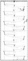
도 10은 본 발명의 일 실시예에 따른 PWM 및 FM 제어를 갖는 ZVS 공진 인버터 전류 루프의 시뮬레이션 개략도이다.
도 11a 내지 도 11d는 경부하 상태에서 본 주제의(subject) ZVS 공진 인버터의 일 실시예의 시뮬레이션 그림 및 스코프 파형(scope waveform)을 도시한다.
도 12a 내지 도 12d는 전부하 상태(full load conditions)에서 본 주제의 ZVS 공진 인버터의 일 실시예의 시뮬레이션 그림 및 스코프 파형을 도시한다.1A is a schematic diagram of a power stage for a dielectric barrier discharge device in accordance with an embodiment of the present invention.
FIG. 1B shows a diagram of a series of soft switching schemes and final outputs of a power stage in accordance with an embodiment of the present invention.
Figure 2a is an equivalent electrical model of an ozone cell stack.
FIG. 2B shows a dielectric barrier discharge cell that generates ozone, and a high voltage AC power signal may be provided by the power system of an embodiment of the present invention.
3 is a schematic diagram of a single power train having a resonant inverter power stage in accordance with one embodiment of the present invention.
4 is a block diagram of a dielectric barrier discharge power system in accordance with an embodiment of the present invention.
5A and 5B show a basic block diagram (Fig. 5A) of a PWM and TM current loop control scheme according to a first embodiment of the present invention (Fig. 5A) and a basic block diagram of a system level control scheme with a power loop do.
Figures 6A and 6B show schematic diagrams of the PWM and FM current loop control schemes shown in Figure 5A in accordance with certain embodiments of the present invention.
7 shows a basic block diagram of a PWM and FM current loop control scheme according to a second embodiment of the present invention.
8 shows a basic block diagram of a PWM and FM current loop control scheme according to a third embodiment of the present invention.
9 shows a basic block diagram of a PWM and FM current loop control scheme according to a fourth embodiment of the present invention.
10 is a simulation schematic diagram of a ZVS resonant inverter current loop with PWM and FM control in accordance with an embodiment of the invention.
FIGS. 11A to 11D show a simulation picture and a scope waveform of an embodiment of a subject ZVS resonant inverter in a light load state. FIG.
Figures 12A-12D illustrate simulation and scope waveforms of one embodiment of a ZVS resonant inverter of the present subject matter in full load conditions.
본원에는 오존 발생기를 포함하여 유전체 장벽 방전기를 위한 개선된 제어 및 전력 출력을 가능하게 하는 기술과 회로가 개시된다.Disclosed herein are techniques and circuits that enable improved control and power output for a dielectric barrier discharge including an ozone generator.
본 발명의 일 실시예에 따르면, 완전 전력을 통해 오존을 발생하는데 요구되는 출력 전력 미만에서 동작하는 능력을 제공하면서 증가된 출력 전력을 가능하게하는 전력 시스템 및 전력 제어 기술이 제공된다. 본 발명의 구체적인 구현예에 따르면, 약 20-40kHz의 주파수 범위와 10kW의 출력 전력의 전력 시스템이 10kW의 ~1% 이하에 대한 제어로 제공된다. 구체적인 실시예에서, 5kW 출력 전력이 각기 가능한 두 개의 전력 트레인이 10kW 출력 전력을 달성하는데 이용된다.According to one embodiment of the present invention, a power system and a power control technique are provided that enable increased output power while providing the ability to operate below the output power required to generate ozone through full power. According to a specific embodiment of the invention, a power system with a frequency range of about 20-40 kHz and an output power of 10 kW is provided for control of less than 1% of 10 kW. In a specific embodiment, two power trains, each capable of 5 kW output power, are used to achieve 10 kW output power.
도 1a는 본 발명의 일 실시예에 따라 유전체 정벽 방전기를 위한 전력 스테이지의 기본도를 예시한다. 도 1a에 도시된 전력 스테이지에서, 4개의 스위치(121, 122, 123, 124)는 인입 DC 버스 전압 입력(Vbus)을 공진 인덕터 Lr(105)와 오존 셀 스택(110)으로 표시된 병렬 공진 탱크 네트워크를 통해 정현파로 변환하는 풀 브릿지로서 배열된다. 스위치(121, 122, 123, 124)는, 제한적인 것은 아니지만, 바이폴라 접합 트랜지스터(BJT)와; 절연 게이트 바이폴라 접합 트랜지스터(IGBT)와; 금속 산화물 반도체 전계 효과 트랜지스터(MOSFET) 및 고전자 이동도 트랜지스터(HEMTs)를 포함하는 전계 효과 트랜지스터(FET)를 포함한 임의의 적절한 스위치일 수 있다.Figure 1A illustrates a basic diagram of a power stage for a dielectric side wall discharge in accordance with one embodiment of the present invention. 1a, four
공진 탱크(인덕터(105) 단독으로 제공되거나 또는 부하(110)의 캐패시터(111)와 조합하여 제공됨)는 풀 브릿지 전력원으로부터 AC 전압을 수신하고, 제어된 진폭의 고전압 정형파의 형태로 공진(또는 사실상 공진인) AC 전압을 유전체 장벽 방전 셀(110)에게 제공한다. 변압기(도면에는 도시되지 않음)는 신호를 원하는 레벨까지 점증(step up)시키기 위해 포함될 수 있다. 변압기의 효과는 Vout/N으로서 Vout을 나타냄으로써 단순화된 모델로 포함될 수 있으며, 여기서 N은 변압기 권선량이다.A resonant tank (either provided solely by
유전체 장벽 방전기의 셀(혹은 부하)(110)는 병렬 캐패시터(111)와 저항기(112)에 의해 모델링될 수 있다. 비록 캐패시터(111)가 셀(110)의 일부로서 도시되었지만, 모델링된 캐패시터의 캐패시턴스는 셀의 자연 캐패시턴스에 덧붙여서 독립적인 개별 캐패시터를 포함할 수도 있다.The cell (or load) 110 of the dielectric barrier discharge can be modeled by a
도 2a는 오존이 발생될 수 있기 전에 출력에서 요구되는 전압을 고려한 오존 셀 스택의 전기 회로 모델을 도시한다. 특히, 전압 클램프 Do(213)(도 1a의 기본도에는 도시되지 않음)는 오존을 발생하는 유전체 장벽 방전기 셀을 모델링할 때 저항기(212)와 직렬로 포함될 수 있다. 오존 농도는 출력 전력에 비례하므로, 오존 셀은 전압 클램프(213)와 직렬인 저항기(212)에 의해 모델링될 수 있다(예를 들면, 도 3에 도시된 저항기(312)와 전압 클램프(313)를 참조하라). 동작시, 오존은 출력 전압이 클램프의 전압보다 큰 특정 전압에 도달한 이후에 발생될 수 있는데, 이것은 저항기 Ro(212)에서 전력의 소비로서 모델링된다. 만약 출력 전압이 클램프의 전압(Do) 미만이면, Ro(212)는 전류를 도전할 수 없어서 전력 소비를 허용하고, 어떠한 오존 농도도 발생되지 않는다.Figure 2a shows an electrical circuit model of an ozone cell stack that takes into account the voltage required at the output before ozone can be generated. In particular, a voltage clamp Do 213 (not shown in the diagram of FIG. 1A) may be included in series with
출력 캐패시턴스 Co(도 1a의 캐패시터(111)로서 모델링됨)는 Co=Cd0*Cd1/(Cd0+Cd1)로서 주어질 수 있으며, 여기서 Cd0는 직렬의 전압 클램프(213) 및 저항기(212)와 병렬인 캐패시터(211)이고, Cd1은 접지된 캐패시터(214)이다.The output capacitance Co (modeled as the
도 2b는 자신의 고전압 AC 전력을 제공하기 위해 본원에 설명된 전력 스테이지 구성을 이용할 수 있는 유전체 장벽 방전 셀의 한 유형을 나타낸다. 도 2b에 도시된 것처럼, 셀(200)은 AC 전력(201)의 인가시 제 1 유전체 장벽막(203)으로부터 갭(204)을 거쳐 제 2 전극(205)으로 전기 방전(202)을 발생하는 제 1 전극(도시 안 됨)을 포함할 수 있다. 선택적인 제 2 유전체 장벽막(도시 안 됨)이 제 2 전극(205)상에 배치될 수 있다. 제 2 전극(205)으로부터 접지로 전하를 운반하는데 물이 이용될 수 있다. 구체적인 실시예에서, 제 1 유전체 장벽막(203)은 산화 알루미늄(Al2O3)으로 형성되고, 제 2 전극(205)은 텅스텐으로 형성된다.Figure 2B illustrates one type of dielectric barrier discharge cell that can utilize the power stage configuration described herein to provide its high voltage AC power. 2B, the
오존 발생 응용인 경우, 갭을 통과하는 산소(O2)는 갭 양단의 전기 방전에 의해 산소 원자로 쪼개져서, 산소 원자가 오존(O3)과 산소(O2)의 혼합물로 재결합될 수 있게 한다.In the case of ozone generation applications, oxygen (O 2 ) passing through the gap is split into oxygen atoms by electrical discharge across the gap, allowing oxygen atoms to recombine into a mixture of ozone (O 3 ) and oxygen (O 2 ).
도 3은 본 발명의 일 실시예에 따른 공진 인버터 전력 스테이지를 갖는 단일 전력 트레인의 개략도이다. 전력 트레인은 본 발명의 일 실시예에 따라 오존 발생기를 모델링하는데 이용될 수 있는 유전체 정벽 방전 셀의 전기 모델을 포함한다. 도 3에 도시된 것처럼, 전력 스테이지 인버터(320)의 스위치는 IGBT(321, 322, 323, 324)를 이용하여 구현되는데, 이것은 풀 브릿지내에 배열되며 인입 DC 버스 전압 입력(Vbus)을 병렬 공진 탱크 네트워크를 통해(공진 탱크(330), 변압기(340) 및 오존 셀 스택(310)을 통해) 정현파형으로 변환한다. 비록 IGBT가 도 3에 도시된 실시예와 관련하여 예시 및 설명되었지만, 실시예가 이것에만 제한되는 것은 아니며, 다른 적절한 트랜지스터 유형이 이용될 수도 있음을 유의해야 한다.3 is a schematic diagram of a single power train having a resonant inverter power stage in accordance with one embodiment of the present invention. The power train includes an electrical model of a dielectric-sited-wall discharge cell that can be used to model an ozone generator in accordance with one embodiment of the present invention. 3, the switches of the
공진 탱크(330)는 전력 스테이지(320)의 풀 브릿지 IGBT와 고전압 변압기(340)를 드라이브 회로내의 비대칭성으로 인한 장해로부터 보호하는 블로킹 캐패시터(blocking capacitor) Cb(331)와; 공진 인덕터 Lr(325)(이것은 변압기 누설 인덕턴스를 포함할 수 있다)와; 고전압 점증 변압기 Xfm(340)(자화된 인덕턴스 Lm(341)를 가짐)와; 오존 부하 셀 스택(310)(캐패시턴스 Co(311), 임피던스 Ro(312)및 클램프 전압 Do(313)를 가짐)을 포함할 수 있다. 5kW 단일 전력 트레인으로, 변압기 출력 전압은 전 출력 부하 동작(full output load operation)에서 30kHz의 스위칭 주파수(fsw) 부근에서 약 8kV 피크-피크까지 점증할 수 있다. 공진 탱크의 주파수 fres는 ![]()
![]()
![]()
![]()
비록 도면에는 도시되지 않았더라도, 제한하는 것은 아니지만, 성분들의 성능을 개선하거나 최적화하기 위한 목적으로 유전체 장벽 방전 전력 시스템내에 추가 회로가 포함될 수도 있다. 예를 들어, 전력 스테이지 공진 탱크의 회로내에는 성분들의 허용한계(tolerance)에 다양한 변화가 있을 수 있고, 이러한 변화는 전력 스테이지의 성능을 열화하는 방식으로 Fres에 영향을 미칠 수 있다. 따라서, 일부 실시예에서, 공진 주파수 fres보다 살짝 높은 주파수(~40kHz)로부터 시작해서 인버터 출력 공진 탱크의 곡선을 따라가면서 추척함으로써 동작하는 튜닝 회로(tuning circuit)가 포함될 수 있다. 이러한 추적은 원하는 입력 전력이 달성될 때 중지된다. 이런 유형의 회로를 피크 전력 포인트 검색 회로(peak power point search circuit)라고 할 수 있다. 이 회로는 전력 스테이지의 개별 인버터가 최대 출력 전력을 발생하는 것을 보장하는데 이용된다. 이런 회로의 예시적인 실시예는 미국 특허 출원 공개 번호 제2007/0108040호에 설명되며, 이 미국 출원은 본원에서 전체적으로 참조하고 있다. 이러한 자동 셀프-튜닝(auto self-tuning) 설계는 인버터 전력 스테이지의 성분 허용한계, 스위칭 주파수 변화, 온도 변화 및 오존 셀 스택 노화를 복사한다는 점에서 일부 유리한 점을 제공한다.Although not shown in the drawings, additional circuitry may be included within the dielectric barrier discharge power system for purposes of, but not limited to, improving or optimizing the performance of components. For example, there may be various variations in the tolerance of the components in the circuit of the power stage resonant tank, and such a change may affect the Fres in a manner that degrades the performance of the power stage. Thus, in some embodiments, a tuning circuit may be included that operates by tracking along the curve of the inverter output resonance tank starting at a frequency slightly higher than the resonance frequency fres (~ 40 kHz). This tracking stops when the desired input power is achieved. This type of circuit can be called a peak power point search circuit. This circuit is used to ensure that individual inverters of the power stage generate the maximum output power. An exemplary embodiment of such a circuit is described in U.S. Patent Application Publication No. 2007/0108040, which is incorporated herein by reference in its entirety. This automatic self-tuning design offers some advantages in that it replicates component tolerances, switching frequency variations, temperature changes, and ozone cell stack aging of the inverter power stage.
도 1a로 다시 돌아가서, 제어 신호 A는 제 1 스위치(121)를 구동하고, 제어 신호 B는 제 2 스위치(122)를 구동하며, 제어 신호 C는 제 3 스위치(123)를 구동하고, 제어 신호 D는 제 4 스위치(124)를 구동한다. 동작시, 제어 신호 A 및 D는 정현 파형의 하부 레일(lower rail)에 대해 제 1 스위치(121)와 제 4 스위치(124)를 각각 턴-온하는데 이용되고, 제어 신호 B 및 C는 정현 파형의 상부 레일(higher rail)에 대해 제 2 스위치(122)와 제 3 스위치(123)를 각각 턴-온하는데 이용된다. 단순화된 타이밍도가 도 1b에 도시되는데, 이 도면은 본 발명의 일 실시예에 따른 영 전압 스위치(ZVS) 스위칭 방식 및 그 결과 출력 응답을 예시한다. ZVS 스위칭 방식은 소프트 스위칭 기술이다. 소프트 스위칭 기술은 영 전압에서 스위칭-온하고 영 전류에서 스위칭-오프하는데 공진 기술을 이용한다. 무시 가능한 스위칭 손실이 이 장치에서 발생할 수 있다.1A, the control signal A drives the
도 1b에 도시된 것처럼, 제어 신호에 위상 변이를 병합함으로써, 모든 스위치를 오프함으로써 초래되는 출력 전압에서의 링잉(ringing)을 최소화하는 것이 가능하다. A 및 D 제어 신호와, B 및 C 제어 신호에 대해 이용되는 위상 변이량은 시스템의 함수이며, 본 주제의 전력 스테이지가 이용되는 특정 시스템에서의 링잉을 막기 위한 임의의 적절한 위상 변이일 수 있다.As shown in Fig. 1B, it is possible to minimize ringing at the output voltage caused by turning all switches off by merging the phase shift in the control signal. The amount of phase shift used for the A and D control signals and the B and C control signals is a function of the system and can be any suitable phase shift to prevent ringing in the particular system in which the power stage of this subject is used.
본 발명의 다양한 실시예에 따르면, 전력 스테이지 제어 신호 A, B, C 및 D는 위상 변이 ZVS를 위해 조합형 펄스 폭 변조(PWM) 및 주파수 변조(FM) 제어 방식을 통해 발생된다.According to various embodiments of the present invention, the power stage control signals A, B, C, and D are generated via a combined pulse width modulation (PWM) and frequency modulation (FM) control scheme for the phase shift ZVS.
도 4는 본 발명의 일 실시예에 따른 유전체 장벽 방전기 시스템의 블록도를 도시한다. 도 4를 참조하면, 전력 스테이지(410)는 고전압 AC 전력을 부하(420)에 제공하기 위해서 DC 버스 전압 VDC를 AC 신호로 변환한다. 특정 실시예에서, 전력 스테이지(410)의 구성과 부하(420)는 도 1a 및/또는 도 3에 도시된 것처럼 배열된다. 전력 스테이지 제어 신호 A, B, C 및 D는 피드백 루프의 일부를 형성하는 제어 회로(430)에 의해 발생 및 제어된다. 제어 회로(430)는 FM 제어와 조합된 위상 변이 ZVS PWM을 포함할 수 있다. 특정 실시예로, 전력 스테이지 제어 신호를 위한 신호 발생기는 위상 변조 및 가변 주파수 가능 PWM 칩이다. 물론, 일부 실시예로, 위상, 듀티 사이클 및 주파수의 제어를 가능하게 하는 임의의 회로 또는 칩이 이용될 수 있는데, 여기서 출력 신호의 적어도 듀티 사이클과 주파수는 이 회로나 칩에 대한 하나 이상의 입력에 의해 조정될 수 있다. 제어 신호 A, B, C 및 D의 펄스폭은 제어 회로(430)의 PWM 피드백 제어 방식에 의해 제어되고, 제어 신호 A, B, C 및 D의 주파수는 제어 회로(430)의 FM 피드백 제어 방식에 의해 제어된다. 특정 실시예에 따르면, PWM 및 FM 피드백 제어 방식은 전류 루프 제어 방식으로 구현되며, 여기서 출력 전류는 전력 스테이지의 출력에서 감지되어, 전력 스테이지에 되공급되는 신호의 펄스폭 및 주파수를 제어하는데 이용된다.4 shows a block diagram of a dielectric barrier discharge system in accordance with an embodiment of the present invention. 4, the
일 실시예에 따르면, PWM 제어와 PM의 통합은 단독의 PWM 기반 제어 방식의 경부하 하드 스위칭에 대항한다. 경부하에서는 인버터 출력 전압의 펄스폭이 크게 감소하므로 하드 스위칭이 일어난다. 이후에 이것은 공진 인덕터의 전류가 그에 따라 크게 감소하게 만든다. 그러므로, 공진 인덕터에 충분히 저장된 에너지가 없다면, 반도체 전력 장치는 소프트 스위칭을 더 이상 지속시키지 못한다.According to one embodiment, the integration of the PWM control and the PM is against light load hard switching of a single PWM based control scheme. Under the light load, the pulse width of the inverter output voltage is greatly reduced and hard switching occurs. This in turn causes the resonant inductor's current to decrease accordingly. Therefore, if there is not enough stored energy in the resonant inductor, the semiconductor power device will no longer sustain soft switching.
하드 스위칭에서, 접합 캐패시턴스에 저장된 에너지는 각각의 턴-온에서 트랜지스터로 방전된다. 그러므로, 하드 스위칭은 전력 손실, 전압/전류 스파이크(spike) 및 전자기 간섭(EMI) 문제들을 초래할 수 있다. 본원에 설명된 소프트 스위칭 토폴로지와 함께 조합형 PWM 및 FM 제어 방식은 추가의 냉각 시스템에 대한 필요성을 없앤다. 예를 들어, 전술한 것처럼, 스위칭 신호를 제어하는데 오로지 PWM만 이용될 때, 하드 스위칭이 경부하에서 발생할 수도 있다. 이와 대조적으로, 본 발명의 일 실시예의 조합형 PWM 및 FM 제어 방식은 모든 부하(전부하 및 경부하)에 대해 소프트 스위칭을 가능하게 한다.In hard switching, the energy stored in the junction capacitance is discharged to the transistor at each turn-on. Therefore, hard switching can result in power loss, voltage / current spikes, and electromagnetic interference (EMI) problems. Combined PWM and FM control schemes with the soft switching topologies described herein eliminate the need for additional cooling systems. For example, as described above, when only PWM is used to control the switching signal, hard switching may occur at light loads. In contrast, the combined PWM and FM control scheme of an embodiment of the present invention enables soft switching for all loads (full load and light load).
"경부하" 조건은 특정 시스템에 따르며, 일반적으로 전부하의 약 5%인 것으로 이해된다. 실제로, 경부하와 관련한 특정 비율은 오존이 계속 발생될 수 있는 비율이다. 본 개시물에서 예로서 예시된 것처럼, 본 발명의 실시예는 전부하의 5% 미만에서 동작할 수 있고, 오존이 발생되지 않을 때에도 기능할 수 있다.The "light load" condition is dependent on the particular system and is generally understood to be about 5% of the total load. In fact, the specific rate associated with light load is the rate at which ozone can still be generated. As illustrated by way of example in this disclosure, embodiments of the present invention can operate at less than 5% of full load and can function even when no ozone is generated.
동작시, 본 주제의 조합형 PWM 및 FM 제어 방식은 경부하에서 주파수를 증가시켜서, 이전에 감소된 펄스폭이 무시될 수 있게 한다. 동작동안, PWM 및 FM 제어 방식은 병렬로 실행되지만, PWM과 FM에 제공되는 가중치는 부하 상태의 변화에 따라 가변한다. 이것은 개선된 동적 범위 성능을 가져온다. 예를 들어, 정규 동작(전부하를 포함한)에서, 듀티 사이클은 오존 출력 전력을 제어하는데 이용되고, 반면에 경부하와 관련해서는 스위칭 주파수를 증가시킴으로써 이 전력이 더 감소된다. 또한, 특정 실시예에서 전력 시스템의 전력 스테이지가 최대 출력 전력의 0%까지 떨어지게 소프트 스위칭(예컨대, 영전압 스위칭)하도록 구성되므로, 전력 시스템의 신뢰성이 개선될 수 있다.In operation, the combined PWM and FM control schemes of the present subject matter increase the frequency under light load, allowing previously reduced pulse widths to be ignored. During operation, the PWM and FM control schemes run in parallel, but the weights provided to PWM and FM vary with changes in load conditions. This results in improved dynamic range performance. For example, in normal operation (including full load), the duty cycle is used to control the ozone output power, while with respect to light load this power is further reduced by increasing the switching frequency. Further, the reliability of the power system can be improved since, in certain embodiments, the power stage of the power system is configured to soft-switch (e. G., Zero voltage switching) to less than 0% of the maximum output power.
도 5a는 일 실시예에 따른 전류 루프 제어 방식의 블록도를 도시한다. 이 도면은 완벽한 전류 루프 제어 방식을 위한 각각의 개별 이득의 전달 함수 블록을 제공한다. 함수 블록은 전치 증폭기 이득 블록(Pre-amp Gain Bock)(501), 전류 루프 보상 이득 블록(current loop Compensation Gain Bock)(502), PWM 이득 블록(503), FM 이득 블록(504), 공진 탱크 및 부하 이득 블록(505) 및 피드백 이득 블록(506)을 포함한다.5A shows a block diagram of a current loop control scheme in accordance with one embodiment. This figure provides a transfer function block for each discrete gain for a complete current loop control scheme. The function block includes a pre-amplifier gain block 501, a current loop
일 실시예에 따르면, 전류 루프내의 각각의 개별 이득 블록의 수식은 다음과 같다.According to one embodiment, the formula of each discrete gain block in the current loop is:
"전치 증폭기 이득 블록""Preamplifier gain block"
![]()
![]()
전류 루프 "보상기 이득 블록"Current Loop "Compensator Gain Block"
![]()
![]()
"공진 탱크 및 부하 이득 블록""Resonant tank and load gain block"
![]()
![]()
예를 들어,E.g,
![]()
![]()
![]()
![]()
전류 "피드백 이득 블록"Current "feedback gain block"
![]()
![]()
PWM 이득 블록 및 FM 이득 블록과 관련해서는, Kpwm≠Kfm=상수이다.With respect to the PWM gain block and the FM gain block, Kpwm ≠ Kfm = constant.
도 5a를 참조하면, 전류 설정 포인트(Iset)가 특정 값으로 제공된다. 특정 실시예에서, 이것은 프로세서를 이용하여 수행될 수 있다(도 5b와 관련한 이하의 설명을 참조하라). 또한, 인버터 전력 스테이지(도 4의 도면부호(410) 참조하며, 도 5a에 도시된 것처럼 공진 탱크 및 부하 이득 블록(505)을 포함함)로부터 출력된 실제 전류(Iout)는 전류 센서에 의해 측정될 수 있으며, 피드백 이득 블록(506)을 통해 피드백 루프로 입력될 수 있다. Iset(이것은 전치 증폭기 이득 블록(501)에 대응하는 전치 증폭기 스테이지를 통해 증폭될 수도 있다)와 피드백 이득 블록(506)으로부터 출력된 전류(Ifbk)는 대표적인 이득 블록(502)을 갖는 전류 루프 보상기에서 더해진다. 다음, 이 이득 스테이지의 출력은 위상 변이 PWM 및 FM 제어기 회로 또는 칩(대응하는 PWM 이득 블록(503)과 FM 이득 블록(504)을 가짐)에 이해 이용되어, 전력 스테이지의 게이트 드라이브(도 6a 및 도 6b 참조)에 대해 스위칭 주파수(Fsw)를 발생시킨다. 피드백 루프는 Iset 값과 동일한 레벨로 출력 전류를 유지하는 방식으로 수행한다.Referring to FIG. 5A, a current set point Iset is provided as a specific value. In certain embodiments, this may be done using a processor (see the discussion below with respect to Figure 5b). Also, the actual current Iout output from the inverter power stage (
경부하의 경우, 전류 루프 보상기 이득 블록(503)은 PWM 칩의 클록의 주파수 시상수(frequency time constant)를 변경하는데 이용되는데, 이것은 주파수 변조로 하여금 Fsw가 시상수에 역비례하므로 발생하게 한다. 그러므로, 전력이 순간적으로 떨어질 때 주파수 변조 제어는 주파수를 낮추어 전력이 적절한 레벨로 유지될 수 있도록 한다.At light load, the current loop compensator gain block 503 is used to change the frequency time constant of the clock of the PWM chip, which causes frequency modulation to occur because Fsw is inversely proportional to the time constant. Therefore, when power momentarily drops, the frequency modulation control lowers the frequency so that the power can be maintained at an appropriate level.
도 5a에 도시된 전류 루프 도면은 아날로그 제어 방식을 예시한다. 다른 실시예로, 도 5a에 도시된 아날로그 제어 방식을 대신하거나 또는 추가적으로 도 5b에 도시된 것같은 디지털 제어 방식이 활용될 수 있다. 도 5b는 ZVS 공진 인버터를 위한 제어 방식의 전력 루프와 내부 전류 루프를 갖는 시스템 수준 도면을 제공한다. 전류 루프 부분은 도 5a와 관련하여 설명된 것과 유사하게 기능을 수행한다. 일 실시예에 따르면, 전력 루프는 디지털 제어 방식을 이용하고, 전력 루프는 프로세서를 이용하여 구현된다. 제한하려는 것은 아니지만, 프로세서는 저가의 마이크로프로세서(μP) 또는 디지털 신호 처리기(DSP)일 수 있다. 메모리는 프로세서의 일부로 포함될 수도 있고, 또는 별도의 성분으로 포함될 수도 있다. 동작시, 마이크로프로세서는 전력 설정 포인트(Pset)를 발행한다. 또한, 실제 입력 전력은 두 개의 DC 입력 공급원(Kvb(s)(508a) 및 Kib(s)(508b)같은)으로부터의 이득과 스케일링되어 입력 전력 이득 블록과 함께 곱셈된 DC 버스 전압(도 4의 VDC 또는 도 1 및 도 3에 도시된 Vbus) 및 DC 버스 전류(도 1 및 도 3의 Ibus 참조)를 이용하여 측정된다. 스케일링 및 곱셈된 DC 입력 공급원의 곱은 전력 피드백 신호(Pfbk)를 만든다. 전력 설정 포인트 Pset과 전력 피드백 Pfbk는 함께 더해져서 디지털 전력 루프 보상기(PID)로 공급된다. PID의 출력은 도 5a와 관련해 설명된 것처럼 전류 설정 포인트 Iset이다.The current loop diagram shown in Figure 5A illustrates an analog control scheme. In another embodiment, a digital control scheme may be utilized in place of or in addition to the analog control scheme shown in FIG. 5A, such as that shown in FIG. 5B. Figure 5b provides a system-level diagram with a controlled power loop and an internal current loop for a ZVS resonant inverter. The current loop portion performs a function similar to that described with respect to FIG. 5A. According to one embodiment, the power loop utilizes a digital control scheme and the power loop is implemented using a processor. Although not intended to be limiting, a processor may be a low cost microprocessor (μP) or a digital signal processor (DSP). The memory may be included as part of the processor, or it may be included as a separate component. In operation, the microprocessor issues a power set point (Pset). In addition, the actual input power is scaled with the gain from the two DC input sources (such as Kvb (s) 508a and Kib (s) 508b) to produce a DC bus voltage multiplied with the input power gain block V DC or Vbus shown in Figures 1 and 3) and the DC bus current (see Ibus in Figures 1 and 3). The product of the scaled and multiplied DC input sources produces a power feedback signal (Pfbk). The power set point Pset and the power feedback Pfbk are added together and fed to the digital power loop compensator (PID). The output of the PID is the current setpoint Iset as described in connection with FIG.
도 5a에서처럼, 도 5b에 도시된 도면은 전력 루프(내부 전류 루프와 함께 제어 방식에 대해 각각의 개별 이득의 전달 함수 블록을 제공한다. 일 실시예에 따르면, 전류 루프내의 각각의 개별 이득 블록의 수식은 도 5a와 관련해 제공된 것처럼 표현될 수 있으며, 전력 루프에 대한 각각의 개별 이득 블록은 다음과 같이 표현될 수 있다.As shown in Figure 5A, the diagram shown in Figure 5B provides a transfer function block of each discrete gain for a control scheme with a power loop (with an internal current loop.) According to one embodiment, each individual gain block The equation can be expressed as provided in connection with FIG. 5A, and each individual gain block for the power loop can be expressed as:
"디지털 전력 루프 보상기 이득 블록""Digital Power Loop Compensator Gain Block"
![]()
![]()
여기서, z=es / Fclk이고, Fclk=μP_Clock(프로세서로부터의 클록의 주파수)이다.Where z = e s / Fclk and Fclk = μP_Clock (the frequency of the clock from the processor).
입력 전력 이득 블록에 대해, 전력 피드백 버스 전압 "Vbus" 이득 블록은 다음과 같이 표현될 수 있다.For the input power gain block, the power feedback bus voltage "Vbus" gain block may be expressed as:
![]()
![]()
그리고 전력 피드백 버스 전류 "Ibus" 이득 블록은 다음과 같이 표현될 수 있다.And the power feedback bus current "Ibus" gain block can be expressed as:
![]()
![]()
분석을 단순화하기 위해 고차 고조파(기본 고조파에 대한)는 무시하면서 모델의 성분들은 이상화되었음을 이해해야 한다.To simplify the analysis, it is important to understand that the components of the model are idealized, ignoring the higher order harmonics (for fundamental harmonics).
다른 실시예에서, 입력 전력을 제어(그리고 도 5b에 예시된 전력 루프를 이용)하는 대신에 출력 부하 전력 제어가 이용될 수 있다. 예를 들어, 인버터 스테이지의 출력에서 감지되는 출력 오존 전압 및 인버터 전류는 제어 루프의 일부로서 이용될 수 있다. 오존 셀이 복소 임피던스처럼 동작하고 전류와 전압은 둘 다 적절히 고주파수이므로, 대역폭, 슬루율(slew rate), 샘플링 시간 및 다른 요인들은 전류와 전압의 곱을 실시간으로 찾기 위해 요구된다.In another embodiment, instead of controlling the input power (and using the power loop illustrated in Figure 5B), an output load power control may be used. For example, the output ozone voltage and inverter current sensed at the output of the inverter stage may be used as part of the control loop. Because the ozone cell behaves like a complex impedance and both current and voltage are properly high frequencies, bandwidth, slew rate, sampling time, and other factors are required to find the product of the current and voltage in real time.
또다른 실시예에서, 도 5b에 도시된 전력 루프는 오존 농도에 기반하여 폐쇄(closed)될 수 있다. 예를 들어, 오존 셀로부터의 오존 농도가 농도 트랜스듀서(concentration transducer)로 측정될 수 있고, 이 트랜스듀서의 출력은 전력 루프를 닫는데 이용될 수 있다.In yet another embodiment, the power loop shown in Figure 5B may be closed based on ozone concentration. For example, the ozone concentration from the ozone cell can be measured with a concentration transducer, and the output of this transducer can be used to close the power loop.
도 6a 및 도 6b는 도 5a와 관련하여 설명된 제어 방식을 따르는 두 개의 예시적인 전류 루프 회로 구현을 예시한다. 도 6a 및 도 6b에 도시된 것처럼, 인버테 스테이지의 출력에서의 전류는 전류 센서(601)에 의해 측정되고, Iset와 함께 전류 루프 오차 증폭기 보상기(602)에 공급된다. 일 실시예로, 도 6a에 도시된 것처럼, Iset은 전류 루프 오차 증폭기 보상기(602)의 정극성 입력 단자에 대한 입력으로서 제공되고, Ifbk는 전류 루프 오차 증폭기 보상기(602)의 부극성 입력 단자에 대한 입력으로서 제공된다. 다른 실시예에서, 도 6b에 도시된 것처럼, Iset 및 Ifbk는 합산되어, 둘 다 전류 루프 오차 증폭기 보상기(602)의 부극성 입력 단자에 제공된다. 오차 증폭기 보상기(602)의 출력은 위상 변이 PWM 제어기(603)에 대한 듀티 사이클 커맨드를 제공하고, PWM 제어기(603)가 게이트 드라이버(604)에 대해 스위칭 주파수 Fsw를 발생할 수 있게 한다. 스위칭 주파수는 오차 증폭기 보상기(602)의 출력을 수신하여 PWM 제어기(603)로 신호를 출력하는 인버팅 증폭기(605)를 통해 주파수 변조될 수 있다. 인버팅 증폭기(605)의 출력은 PWM 클록의 주파수 시상수를 변경하여, 주파수 변조가 일어나게 한다.Figures 6A and 6B illustrate two exemplary current loop circuit implementations that follow the control scheme described with respect to Figure 5A. 6A and 6B, the current at the output of the invert stage is measured by the
게이트 드라이버(604)는 예컨대 도 1a 및 도 1b와 관련하여 설명된 것(스위치(121, 122, 123, 124)) 및 도 3과 관련하여 설명된 것(전력 스테이지(320)이 스위치(321, 322, 323, 324))같은 풀 브릿지 인버터 스테이지에 대해 제어 신호 A, B, C 및 D를 발생한다.The
PWM 제어기(603)와 연결된 캐패시터 Ct와 저항기 Rt는 인버팅 증폭기(605)로부터의 전류 보상 신호에 의해 조정되는 초기 고정 주파수(initial fixed frequency)를 제공한다. 도 6a 및 도 6b에 도시된 인버팅 증폭기 구성에서, op-증폭기는 듀티 사이클(펄스폭)을 제어하는데 이용되는 신호의 배수(또는 분수)로 주파수 변조를 제어하는데 이용되는 신호를 조정하는데 이용될 수 있다. 다른 실시예로, FM 제어를 위한 증폭기의 이득은 가변 이득 증폭기를 이용함으로써 가변될 수 있다. 프로세서가 전송한 이득 제어 신호를 이용하여 이득이 제어될 수도 있다. 일 실시예로, 특정 조건이 충족될 때, 프로세서와 연관된 메모리내에 저장된 사전설정 변경(preset modification)이 이용될 수도 있다. 다른 실시예에서, 이들 조정의 사용자 제어를 가능하게 하기 위해 사용자 인터페이스가 포함될 수도 있다. 사용자 인터페이스는 프로세서에 연결되어 프로세서와 통신할 수도 있다. 선택적으로, 또는 추가적으로, 사용자 인터페이스가 전위차계(potentiometer)를 통한 저항의 수동 조정을 포함할 수도 있다(이것은 예컨대 도 6a의 R4 또는 도 6b의 R4를 조정할 수 있다).The capacitor Ct and the resistor Rt connected to the
도 7 내지 도 9는 본 발명의 일부 실시예에 따른 전류 루프 구성을 예시한다. 예를 들어, 도 7을 참조하면, 제 2 실시예에 따른 전류 루프 제어 방식은 도 5a에 도시된 방식과 유사하다. 그러나, 전력 스테이지의 게이트 드라이브(도 6a 및 도 6b의 도면부호(604) 참조)를 위한 스위칭 주파수(Fsw)를 발행하기 위해 위상 변이 PWM 및 FM 제어기에 의해 이용되는 보상기 이득 블록(702) 스테이지의 출력을 대신하여, 전류 루프 보상기와 병렬로 FM 이득 블록(704) 스테이지가 Iset(전치 증폭기 이득 블록(701)에 대응하는 전치 증폭기 스테이지를 통해 증폭될 수 있음)와, 피드백 이득 블록(706)으로부터 출력된 전류(Ifbk)를 수용한다.7-9 illustrate a current loop configuration according to some embodiments of the present invention. For example, referring to FIG. 7, the current loop control scheme according to the second embodiment is similar to that shown in FIG. 5A. However, the phase of the
도 8에 도시된 실시예의 경우, FM 이득 블록(804) 스테이지는 Iset 전류와 도 5a 또는 도 7과 관련해 설명된 것같은 피드백 이득 블록(806)으로부터 피드백 전류를 대신해 주파수를 제어하기 위해 입력 전력을 이용한다. 예를 들어, DC 버스 전압(도 4의 VDC 또는 도 1 및 도 3에 도시된 Vbus)과 DC 버스 전류(도 1 및 도 3의 Ibus 참조)는 두 개의 DC 입력 공급원(Kvb(s)(808a) 및 Kib(s)(808b)같은)으로부터의 이득과 스케일링되고, FM 이득 블록(804)을 통해 입력되기 전에 함께 곱셈된다.8, the
도 9에 도시된 실시예의 경우, FM 이득 블록(904) 스테이지는 도 8과 관련해 설명된 것처럼 입력 전력을 대신하여 주파수를 제어하기 위해 출력 전력을 이용한다.For the embodiment shown in FIG. 9, the
특정 실시예로, 도 5b와 관련해 설명된 전력 루프 부분은 도 7 내지 도 9에 도시된 전류 루프 중 하나로 구성될 수 있다.In a particular embodiment, the portion of the power loop described with respect to FIG. 5B may be comprised of one of the current loops shown in FIGS.
바람직하게는, 특정 실시예로, 전력을 유지하면서 전력선 변화를 수용하는 표준이 공간을 차지하면서 추가적인 냉각 기술도 요구할 수 있는 별도의 회로나 보호 캐패시터를 요구하지 않으면서 충족될 수 있다. 특히, 주파수 변조 제어를 이용함으로써, 전력선상의 부하로 인한 변화가 스위치를 구동하는 주파수의 변화와 전력선상의 전력을 유지하는 능력을 초래한다. 본 주제의 조합형 PWM 및 FM 제어 방식에 의해 충족될 수 있는 표준의 일 예가 SEMI F47 표준 "Specification for Semiconductor Processing Equipment Voltage Sag Immunity"로, 이것은 반도체 공정, 계측학 및 자동화 테스트 장비에서 이용되는 툴(tool)이 방해없이 끝까지 동작해야 하는 순간 전압 강하 보상 능력(또는 임계)을 정의한다.Preferably, in certain embodiments, a standard that accommodates power line changes while maintaining power can be met without requiring additional circuitry or a protective capacitor that may require additional cooling techniques while occupying space. In particular, by using frequency modulation control, a change due to a load on a power line results in a change in frequency driving the switch and the ability to maintain power on the power line. An example of a standard that can be satisfied by the combined PWM and FM control methods of this topic is the SEMI F47 standard "Specification for Semiconductor Processing Equipment Voltage Sag Immunity", which is a tool used in semiconductor process, ) Defines the instantaneous voltage drop compensation capability (or critical) that must operate to the end without interruption.
본 주제의 전력 시스템과 전력 제어 기술의 실시예는 이전의 시스템의 사이즈를 증가시키지 않으면서 구현될 수 있다. 다양한 실시예에서, 전력 시스템은 동일하거나 더 큰 출력 전력 및 제어를 제공하면서 종래의 비상주(non-resident) 전력 인버터보다 더 밀집한 공간에 설치될 수 있다.Embodiments of the power system and power control techniques of the present subject matter can be implemented without increasing the size of the previous system. In various embodiments, the power system may be installed in a more dense space than a conventional non-resident power inverter while providing the same or greater output power and control.
본 발명의 보다 나은 이해와 많은 이점들은 예시로서 제공된 다음의 예들로부터 제공될 수 있다. 다음의 예는 본 발명의 방법, 응용, 실시예 및 변형 중 일부를 예시하는 것이다. 물론 이들은 어떤 방식으로든 본 발명을 제한하지 않는 것으로 간주되어야 한다. 다양한 변화와 수정이 본 발명과 관련하여 수행될 수 있다.BRIEF DESCRIPTION OF THE DRAWINGS A better understanding of the present invention and many of its advantages can be provided from the following examples, which are provided by way of example. The following examples are illustrative of some of the methods, applications, embodiments and variations of the present invention. Of course, these should not be construed as limiting the invention in any way. Various changes and modifications may be made in connection with the present invention.
Cadence Design Systems, Inc.의 등록된 상표인 PSpice® 회로 시뮬레이터 툴이 본 발명의 일 실시예에 따라 설계된 유전체 장벽 방전기를 시뮬레이트하는데 이용되었다.A PSpice ® circuit simulator tool, a registered trademark of Cadence Design Systems, Inc., was used to simulate a dielectric barrier discharge device designed in accordance with one embodiment of the present invention.
이 예에서, 듀얼 10kW 오존 전력 트레인(전력 트레인당 5kW)을 위한 PSpice® 시뮬레이션은 본 시스템 및 방법의 기능을 예시하는 실험 결과와 비교된다. 도 10은 본 발명의 일 실시예에 따른 범용 ZVS 공진 인버터 전류 루프 설계의 PSpice® 시뮬레이션에 이용되는 PSpice® 회로도를 도시한다. 이 회로도는 도 6b에 도시된 것과 유사한 구현을 따르는데, 여기서 피드백 전류 및 전류 설정 포인트 Iset은 보상기에 입력되기 전에 합산된다. 또한, 전류는 공통 모드 잡음을 막기 위해 차동 증폭기를 이용하여 측정된다. 공진 탱크 및 오존 셀은 도 1a와 관련하여 설명된 인덕터(105), 캐패시터(111) 및 저항기(112) 구성을 이용하여 시뮬레이트된다.In this example, a PSpice ® simulation for a dual 10 kW ozone power train (5 kW per power train) is compared with experimental results illustrating the function of the system and method. 10 illustrates a PSpice ® circuit diagram used in a PSpice ® simulation of a general-purpose ZVS resonant inverter current loop design in accordance with an embodiment of the present invention. This circuit diagram follows an implementation similar to that shown in Figure 6b, where the feedback current and current set point Iset are summed before being input to the compensator. The current is also measured using a differential amplifier to prevent common mode noise. The resonant tank and ozone cell are simulated using the
시뮬레이션을 위해, 입력 Vbus 전압은 저 라인 값에서부터 고 라인 값(200-350 VDC)까지 변화되었고, Iset은 0.5-3.0 VDC(0.5% 내지 110% 부하)에서 전압원을 이용하여 변화되었다. 이러한 두 조건은 예측된 동작 범위를 포함한다.For simulation, the input Vbus voltage was varied from a low line value to a high line value (200-350 VDC), and Iset was varied using a voltage source at 0.5-3.0 VDC (0.5% to 110% load). These two conditions include the expected range of motion.
예 1-경부하(Example 1- Light Load ( LightLight Load) Load)
경부하에서 전류 루프에 대한 시뮬레이션 결과는 도 11a 내지 도 11c에 도시되며, 경부하에서 전류 루프에 대한 실험 결과는 도 11d에 도시된다. 도 11a는 Vbus가 350V에 설정되었음을 보여주고, 경부하 상태는 출력 부하 전력이 25W 미만(5kW 시스템의 최대 출력의 5% 오존 농도의 ~250V 출력 전력 경부하 상태과 비교하여)임을 보여준다. 도 11b는 인버터 스테이지 출력 전압(Vinv)과 전류(Iinv)의 구성도를 도시한다. 도 11c는 전력 스테이지 출력 전압(Vout)과 전류(Iout)의 구성도를 도시한다(즉, 오존 셀로 공급되는 전압과 전류). 도 11d는 실험 시스템과 관련하여 인버터 스테이지 출력 전압 Vinv과 전류 Iinv의 스코프 파형을 도시하며, 여기서 Vbus=300V, Ibus=0.8A, Pin=240W이다. 도 11c에 설명되고 도 11d에 도시된 파형에서 확인할 수 있듯이, PWM과 FM 제어의 조합은 경부하에서도 소프트 스위칭을 가능하게 한다. 시뮬레이션 파형이 0.5% Iset이었고 오존을 발생하는 공정 제한조건으로 인해 실험이 Iset의 ~5%까지 였으므로, 시뮬레이션 및 측정 결과 파형과 관련한 구성도의 스케일은 균일하지 않음을 유의해야 한다.The simulation results for the current loop under light load are shown in Figures 11A-11C and the experimental results for the current loop under light load are shown in Figure 11D. Figure 11a shows that Vbus is set at 350V and the light load condition shows that the output load power is less than 25W (compared to a ~ 250V output power light load of 5% ozone concentration at 5kW system maximum output). Fig. 11B shows a configuration diagram of the inverter stage output voltage Vinv and the current Iinv. 11C shows a schematic diagram of the power stage output voltage Vout and current Iout (i.e., the voltage and current supplied to the ozone cell). Figure 11d shows the scope waveform of the inverter stage output voltage Vinv and current Iinv in relation to the experimental system, where Vbus = 300V, Ibus = 0.8A, Pin = 240W. As can be seen from the waveforms shown in Fig. 11C and shown in Fig. 11D, the combination of PWM and FM control enables soft switching even at light loads. It should be noted that the scale of the schematic associated with the simulation and measurement result waveforms is not uniform since the simulated waveform was 0.5% Iset and the experiment was up to 5% of the Iset due to process constraints that generate ozone.
예2-전부하(Example 2 - Full load ( FullFull Load) Load)
전부하에서 전류 루프에 대한 시뮬레이션 결과가 도 12a 내지 도 12c에 도시되고, 전부하의 110%에서 전류 루프에 대한 실험 결과는 도 11d에 도시된다. 도 12a는 Vbus가 350V였음을 도시하고, 전부하 상태는 약 5.5kW인 출력 부하 전력을 보여준다(단일 스테이지). 도 12b는 인버터 스테이지 출력 전압(Vinv)과 전류(Iinv)의 구성도를 도시한다. 도 12c는 전력 스테이지 출력 전압(Vout)과 전류(Iout)의 구성도를 도시한다(즉, 오존 셀로 공급되는 전압과 전류). 도 12d는 실험 시스템과 관련하여 인버터 스테이지 출력 전압 Vinv과 전류 Iinv의 스코프 파형을 도시하며, 여기서 Vbus=300V, Ibus=18.3A, Pin=~5.5kW이다. 도 12c에 설명되고 도 12d에 도시된 파형에서 확인할 수 있듯이, PWM과 FM 제어의 조합은 소프트 스위칭 및 증가된 출력 전력을 가능하게 한다.The simulation results for the current loop at full load are shown in Figs. 12A to 12C, and the experimental results for the current loop at 110% of full load are shown in Fig. 11D. Figure 12a shows that the Vbus was 350V and the full load state shows an output load power of about 5.5kW (single stage). 12B shows a configuration diagram of the inverter stage output voltage Vinv and the current Iinv. 12C shows a schematic diagram of the power stage output voltage Vout and current Iout (i.e., the voltage and current supplied to the ozone cell). Figure 12d shows the scope waveform of the inverter stage output voltage Vinv and current Iinv in relation to the experimental system, where Vbus = 300V, Ibus = 18.3A, Pin = ~ 5.5kW. As can be seen in the waveforms illustrated in Figure 12C and shown in Figure 12D, the combination of PWM and FM control enables soft switching and increased output power.
본 명세서에서 "일 실시예", "실시예", "예시적인 실시예", "제 2 실시예" 등으로 언급하는 것들은 언급된 실시예와 연계하여 설명된 특정 특징, 구조 또는 특성이 본 발명의 적어도 한 실시예에 포함된다는 것을 의미한다. 여러 곳에서 이러한 표현이 나타나더라도 이것이 모두 반드시 동일한 실시예를 지칭하는 것은 아니다. 또한, 본원에 개시된 모든 발명 또는 발명의 실시예의 모든 요소 또는 제한조건은 (개별적으로 또는 임의의 조합으로) 임의의 및/또는 모든 다른 요소 또는 제한조건과 조합될 수 있거나 또는 본원에 개시된 임의의 다른 발명이나 그 실시예와 조합될 수 있고, 이러한 조합은 모두 제한없이 본 발명의 범주내에 있는 것으로 고려된다.Reference in the specification to "one embodiment", "an embodiment", "an example embodiment", "a second embodiment", etc., means that a particular feature, structure, or characteristic described in connection with the embodiment Quot; is included in at least one embodiment of < / RTI > Wherever such appearances appear in various places, they are not necessarily all referring to the same embodiment. It is also to be understood that all elements or limitations of embodiments of the invention or inventions disclosed herein may be combined (individually or in any combination) with any and / or all of the other elements or limitations, Or combinations thereof, and all such combinations are considered to be within the scope of this invention without being restricted in any way.
본원에 개시된 예들과 실시예는 단지 예시를 목적으로 하는 것임을 이해해야 하며, 그 견지에서 다양한 수정과 변경이 당업자에게 제안될 것이고 이러한 다양한 수정과 변경은 본 출원의 사상과 범주내에 포함되는 것임을 이해해야 한다.It is to be understood that the examples and embodiments disclosed herein are for illustrative purposes only, and that various modifications and changes may be suggested to those skilled in the art, and that these various modifications and changes are encompassed within the spirit and scope of the present application.
Claims (20)
인버터 스테이지(inverter stage)와,
상기 인버터 스테이지의 출력을 수신하고, 적어도 하나의 유전체 장벽 방전 셀에 전력을 공급하기 위한 신호를 출력하는 공진 탱크(resonant tank)와,
제어 회로를 포함하되,
상기 제어 회로는
소프트 스위칭(soft switching)을 위한 위상 변이를 포함하는 스위칭 신호를 상기 인버터 스테이지로 제공하는 게이트 드라이버와,
상기 게이트 드라이버를 위한 스위칭 주파수를 발생시키는 펄스폭 변조(PWM) 제어기―상기 PWM 제어기는, PWM을 수행하기 위해 상기 스위칭 주파수의 듀티 사이클을 조정하는 제 1 신호를 수신하도록 구성된 제 1 입력부와, 주파수 변조(FM)를 수행하기 위해 상기 PWM 제어기의 클록 주파수 시상수(clock frequency time constant)를 조정하는 제 2 신호를 수신하도록 구성된 제 2 입력부를 가짐―를 포함하고,
상기 제어 회로는 상기 인버터 스테이지로부터의 출력 전류를 포함하는 피드백 신호를 수신하고, 상기 피드백 신호를 이용하여 상기 제 1 신호와 상기 제 2 신호를 발생시키는
유전체 장벽 방전 전력 시스템.
A dielectric barrier discharge power system comprising:
An inverter stage,
A resonant tank for receiving the output of the inverter stage and outputting a signal for supplying power to at least one dielectric barrier discharge cell,
And a control circuit,
The control circuit
A gate driver for providing a switching signal to the inverter stage, the switching signal including a phase shift for soft switching;
A pulse width modulation (PWM) controller for generating a switching frequency for the gate driver, the PWM controller comprising: a first input configured to receive a first signal that adjusts a duty cycle of the switching frequency to perform PWM; And a second input configured to receive a second signal that adjusts a clock frequency time constant of the PWM controller to perform modulation (FM)
Wherein the control circuit receives a feedback signal comprising an output current from the inverter stage and generates the first signal and the second signal using the feedback signal
Dielectric barrier discharge power system.
상기 인버터 스테이지는 풀 브릿지(full bridge)로서 배열된 4개의 트랜지스터를 포함하는
유전체 장벽 방전 전력 시스템.
The method according to claim 1,
The inverter stage includes four transistors arranged as full bridges
Dielectric barrier discharge power system.
상기 4개의 트랜지스터는 절연 게이트 바이폴라 트랜지스터(IGBT)인
유전체 장벽 방전 전력 시스템.
3. The method of claim 2,
The four transistors are insulated gate bipolar transistors (IGBTs)
Dielectric barrier discharge power system.
상기 적어도 하나의 유전체 장벽 방전 셀에 전력을 공급하기 위한 상기 공진 탱크로부터의 신호를 점증(stepping up)시키는 변압기를 더 포함하는
유전체 장벽 방전 전력 시스템.
The method according to claim 1,
Further comprising a transformer for stepping up a signal from the resonant tank for supplying power to the at least one dielectric barrier discharge cell
Dielectric barrier discharge power system.
상기 스위칭 주파수는 20kHz 내지 40kHz의 범위내인
유전체 장벽 방전 전력 시스템.
The method according to claim 1,
The switching frequency is in the range of 20 kHz to 40 kHz
Dielectric barrier discharge power system.
상기 스위칭 주파수는 상기 공진 탱크의 공진 주파수보다 더 높게 구성되는
유전체 장벽 방전 전력 시스템.
The method according to claim 1,
Wherein the switching frequency is configured to be higher than the resonance frequency of the resonance tank
Dielectric barrier discharge power system.
상기 피드백 신호는 상기 인버터 스테이지의 출력에서 전류 센서로부터 수신된 측정된 전류 신호(a measured current signal)를 포함하는
유전체 장벽 방전 전력 시스템.
The method according to claim 1,
Wherein the feedback signal comprises a measured current signal received from the current sensor at the output of the inverter stage
Dielectric barrier discharge power system.
전체 부하 상태(all load conditions) 동안, 상기 측정된 전류 신호는 전류 설정 포인트 값(current set point value)과 비교되고, 상기 비교의 오차값은 상기 제 1 신호로 하여금 상기 측정된 전류 신호가 상기 전류 설정 포인트 값에 도달할 때까지 상기 스위칭 주파수의 듀티 사이클을 조정하여 상기 PWM을 수행하게 하고, 상기 비교의 오차값은 또한 상기 제 2 신호로 하여금 상기 클록 주파수 시상수를 변경되도록 조정하여 상기 FM을 수행하게 하며,
상기 유전체 장벽 방전 전력 시스템이 전부하 상태(full load condition)로부터 경부하 상태(light load condition)로 동작할 때 상기 제어 회로는 전력을 제어하기 위한 상기 PWM과 상기 FM에 제공되는 가중치의 양이 변하도록 구성되는
유전체 장벽 방전 전력 시스템.
8. The method of claim 7,
During all load conditions, the measured current signal is compared to a current set point value, and the error value of the comparison causes the first signal to cause the measured current signal to flow through the current Adjusts the duty cycle of the switching frequency to perform the PWM until the set point value is reached, and the error value of the comparison further adjusts the second signal to change the clock frequency time constant to perform the FM However,
When the dielectric barrier discharge power system operates from a full load condition to a light load condition, the control circuit controls the PWM to control power and the amount of weight provided to the FM, It is configured to
Dielectric barrier discharge power system.
상기 제어 회로는 상기 제 1 신호와 상기 제 2 신호를 발생하는 전류 제어 루프를 포함하되, 상기 전류 제어 루프는 상기 인버터 스테이지의 출력에서 감지되는 상기 측정된 전류 신호와 전류 설정 포인트를 이용하는
유전체 장벽 방전 전력 시스템.
8. The method of claim 7,
Wherein the control circuit includes a current control loop for generating the first signal and the second signal, wherein the current control loop is configured to use the measured current signal and the current set point sensed at the output of the inverter stage
Dielectric barrier discharge power system.
상기 전류 제어 루프는
상기 측정된 전류 신호와 상기 전류 설정 포인트를 수신하고, 상기 제 1 신호를 출력하는 오차 증폭기 보상기(error amplifier compensator)와,
상기 제 1 신호를 수신하고, 상기 제 2 신호를 출력하는 인버팅 증폭기(inverting amplifier)를 포함하는
유전체 장벽 방전 전력 시스템.
10. The method of claim 9,
The current control loop
An error amplifier compensator for receiving the measured current signal and the current set point and outputting the first signal;
And an inverting amplifier for receiving the first signal and outputting the second signal,
Dielectric barrier discharge power system.
상기 전류 제어 루프는
상기 측정된 전류 신호와 상기 전류 설정 포인트를 수신하고, 상기 제 1 신호를 출력하는 오차 증폭기 보상기와,
상기 오차 증폭기 보상기의 출력을 수신하고, 상기 제 2 신호를 출력하는 인버팅 증폭기를 포함하는
유전체 장벽 방전 전력 시스템.
10. The method of claim 9,
The current control loop
An error amplifier compensator for receiving the measured current signal and the current set point and outputting the first signal;
And an inverting amplifier for receiving an output of the error amplifier compensator and outputting the second signal
Dielectric barrier discharge power system.
상기 피드백 신호는 입력 전력 신호를 더 포함하되, 상기 입력 전력 신호는 상기 인버터 스테이지에 공급되는 측정된 DC 버스 전압과 상기 인버터 스테이지에 공급되는 측정된 DC 버스 전류의 곱(product)이고,
상기 전류 제어 루프는
상기 측정된 전류 신호와 상기 전류 설정 포인트를 수신하고, 상기 제 1 신호를 출력하는 오차 증폭기 보상기와,
상기 입력 전력 신호를 수신하고, 상기 제 2 신호를 출력하는 인버팅 증폭기를 포함하는
유전체 장벽 방전 전력 시스템.
10. The method of claim 9,
Wherein the feedback signal further comprises an input power signal, wherein the input power signal is a product of a measured DC bus voltage supplied to the inverter stage and a measured DC bus current supplied to the inverter stage,
The current control loop
An error amplifier compensator for receiving the measured current signal and the current set point and outputting the first signal;
And an inverting amplifier for receiving the input power signal and outputting the second signal
Dielectric barrier discharge power system.
상기 피드백 신호는 출력 전력 신호를 더 포함하되, 상기 출력 전력 신호는 측정된 DC 출력 전압과 상기 측정된 전류의 곱이고,
상기 전류 제어 루프는
상기 측정된 전류 신호와 상기 전류 설정 포인트를 수신하고, 상기 제 1 신호를 출력하는 오차 증폭기 보상기와,
상기 출력 전력 신호를 수신하고, 상기 제 2 신호를 출력하는 인버팅 증폭기를 포함하는
유전체 장벽 방전 전력 시스템.
10. The method of claim 9,
Wherein the feedback signal further comprises an output power signal, wherein the output power signal is a product of the measured DC output voltage and the measured current,
The current control loop
An error amplifier compensator for receiving the measured current signal and the current set point and outputting the first signal;
And an inverting amplifier for receiving the output power signal and outputting the second signal
Dielectric barrier discharge power system.
프로세서를 더 포함하되,
상기 프로세서는
상기 인버터 스테이지에 공급되는 DC 버스 전압 및 전류의 측정치를 수신하고―상기 DC 버스 전압 및 전류의 측정치는 전력 피드백 신호를 제공하기 위해 스케일링되어(scaled) 함께 곱해짐―,
상기 전력 피드백 신호를 전력 설정 포인트에 더하고,
상기 전류 제어 루프를 위한 상기 전류 설정 포인트를 출력하기 위해 상기 전력 피드백 신호와 상기 전력 설정 포인트를 이용하여 디지털 오차 보상을 수행하도록 구성되는
유전체 장벽 방전 전력 시스템.
10. The method of claim 9,
Further comprising a processor,
The processor
And receiving a measure of the DC bus voltage and current supplied to the inverter stage, wherein the measurements of the DC bus voltage and current are scaled and multiplied together to provide a power feedback signal,
Adding the power feedback signal to a power set point,
And to perform digital error compensation using the power feedback signal and the power set point to output the current set point for the current control loop
Dielectric barrier discharge power system.
적어도 하나의 유전체 장벽 방전 셀에 전력을 공급하기 위해 인버터 스테이지 및 공진 탱크를 제공하는 단계와,
제어 회로를 이용하여 상기 인버터 스테이지를 위한 스위칭 신호를 발생시키는 단계―상기 스위칭 신호는 소프트 스위칭을 위한 위상 변이를 포함함―를 포함하되,
상기 스위칭 신호를 발생시키는 단계는
상기 인버터 스테이지의 출력 전류를 전류 설정 포인트 값에서 유지하기 위해 상기 스위칭 신호의 스위칭 주파수의 펄스폭 변조(이하, PWM)를 수행하는 단계와,
상기 PWM을 수행하는 단계와 동시에 주파수 변조(이하, FM)를 수행하는 단계―상기 FM은 경부하 상태 동안 출력 전력을 감소시키기 위해 상기 스위칭 신호의 스위칭 주파수를 증가시킴―를 포함하는
유전체 장벽 방전을 발생시키는 방법.
A method of generating a dielectric barrier discharge,
Providing an inverter stage and a resonant tank to supply power to at least one dielectric barrier discharge cell;
Generating a switching signal for the inverter stage using a control circuit, the switching signal comprising a phase shift for soft switching,
The step of generating the switching signal
Performing PWM (Pulse Width Modulation) on the switching frequency of the switching signal to maintain the output current of the inverter stage at a current setpoint value;
Performing frequency modulation (FM) concurrently with performing the PWM, the FM increasing the switching frequency of the switching signal to reduce output power during a light load condition,
A method of generating a dielectric barrier discharge.
상기 스위칭 신호는 20kHz 내지 40kHz의 범위의 주파수를 갖는
유전체 장벽 방전을 발생시키는 방법.
16. The method of claim 15,
Wherein the switching signal has a frequency in the range of 20 kHz to 40 kHz
A method of generating a dielectric barrier discharge.
상기 PWM를 수행하는 단계는
게이트 드라이버를 위해 상기 스위칭 주파수를 발생시키는 PWM 제어기를 제공하는 단계―상기 PWM 제어기는 PWM을 수행하기 위해 상기 스위칭 주파수의 듀티 사이클을 조정하는 제 1 신호를 수신하도록 구성된 제 1 입력부와, FM을 수행하기 위해 상기 PWM 제어기의 클록 주파수 시상수를 조정하는 제 2 신호를 수신하도록 구성된 제 2 입력부를 가짐―와,
상기 인버터 스테이지의 상기 출력 전류를 감지하는 단계와,
오차 증폭기 보상을 수행함으로써 상기 출력 전류를 전류 설정 포인트와 비교하는 단계와,
상기 오차 증폭기 보상을 상기 제 1 신호로서 이용하는 단계를 포함하는
유전체 장벽 방전을 발생시키는 방법.
16. The method of claim 15,
The step of performing the PWM
Providing a PWM controller for generating the switching frequency for a gate driver, the PWM controller comprising: a first input configured to receive a first signal that adjusts a duty cycle of the switching frequency to perform PWM; A second input configured to receive a second signal that adjusts the clock frequency time constant of the PWM controller to provide a second clock signal,
Sensing the output current of the inverter stage;
Comparing the output current to a current setpoint by performing an error amplifier compensation,
And using the error amplifier compensation as the first signal
A method of generating a dielectric barrier discharge.
상기 FM을 수행하는 단계는 상기 제 2 신호를 출력하는 인버팅 증폭기를 이용하여 상기 오차 증폭기 보상을 반전시키는 단계를 포함하는
유전체 장벽 방전을 발생시키는 방법.
18. The method of claim 17,
Wherein performing the FM comprises inverting the error amplifier compensation using an inverting amplifier that outputs the second signal
A method of generating a dielectric barrier discharge.
상기 FM을 수행하는 단계는 상기 인버팅 증폭기의 이득을 조정하는 단계를 더 포함하는
유전체 장벽 방전을 발생시키는 방법.
19. The method of claim 18,
Wherein performing the FM further comprises adjusting a gain of the inverting amplifier
A method of generating a dielectric barrier discharge.
상기 인버터 스테이지에 공급되는 DC 버스 전압의 측정치와, 상기 인버터 스테이지에 공급되는 DC 버스 전류의 측정치를 수신하는 단계―상기 DC 버스 전압의 측정치 및 상기 DC 버스 전류의 측정치는 전력 피드백 신호를 제공하기 위해 스케일링되어 함께 곱해짐―와,
상기 전력 피드백 신호를 전력 설정 포인트에 더하는 단계와,
상기 전류 설정 포인트를 출력하기 위해 상기 전력 피드백 신호와 상기 전력 설정 포인트를 이용하여 디지털 오차 보상을 수행하는 단계를 더 포함하는
유전체 장벽 방전을 발생시키는 방법.18. The method of claim 17,
Receiving a measure of a DC bus voltage supplied to the inverter stage and a measure of a DC bus current supplied to the inverter stage, wherein a measure of the DC bus voltage and a measure of the DC bus current are provided to provide a power feedback signal Scaled and multiplied together -
Adding the power feedback signal to a power setpoint;
And performing digital error compensation using the power feedback signal and the power set point to output the current set point
A method of generating a dielectric barrier discharge.
Applications Claiming Priority (3)
| Application Number | Priority Date | Filing Date | Title |
|---|---|---|---|
| US13/431,521 US8680777B2 (en) | 2012-03-27 | 2012-03-27 | Versatile zero-voltage switch resonant inverter for industrial dielectric barrier discharge generator applications |
| US13/431,521 | 2012-03-27 | ||
| PCT/US2013/032772 WO2013148390A1 (en) | 2012-03-27 | 2013-03-18 | A versatile zero-voltage switch resonant inverter for industrial dielectric barrier discharge generator applications |
Publications (2)
| Publication Number | Publication Date |
|---|---|
| KR20140148443A KR20140148443A (en) | 2014-12-31 |
| KR101665220B1 true KR101665220B1 (en) | 2016-10-11 |
Family
ID=49233996
Family Applications (1)
| Application Number | Title | Priority Date | Filing Date |
|---|---|---|---|
| KR1020147029941A KR101665220B1 (en) | 2012-03-27 | 2013-03-18 | A versatile zero-voltage switch resonant inverter for industrial dielectric barrier discharge generator applications |
Country Status (8)
| Country | Link |
|---|---|
| US (1) | US8680777B2 (en) |
| EP (1) | EP2834911B1 (en) |
| JP (1) | JP5923658B2 (en) |
| KR (1) | KR101665220B1 (en) |
| CN (1) | CN104205604B (en) |
| SG (1) | SG11201404303PA (en) |
| TW (1) | TWI551026B (en) |
| WO (1) | WO2013148390A1 (en) |
Families Citing this family (52)
| Publication number | Priority date | Publication date | Assignee | Title |
|---|---|---|---|---|
| US20140008211A1 (en) | 2012-07-06 | 2014-01-09 | Pacific Ozone Technology, Inc. | Ozone cell power supply apparatus and method |
| US9363862B1 (en) * | 2012-12-05 | 2016-06-07 | Universal Lighting Technologies | Automatic current and reference gain control for wide range current control |
| US9263960B2 (en) * | 2013-09-16 | 2016-02-16 | Delta Electronics, Inc. | Power converters for wide input or output voltage range and control methods thereof |
| US10431428B2 (en) | 2014-01-10 | 2019-10-01 | Reno Technologies, Inc. | System for providing variable capacitance |
| US9865432B1 (en) | 2014-01-10 | 2018-01-09 | Reno Technologies, Inc. | RF impedance matching network |
| US9844127B2 (en) | 2014-01-10 | 2017-12-12 | Reno Technologies, Inc. | High voltage switching circuit |
| US9697991B2 (en) | 2014-01-10 | 2017-07-04 | Reno Technologies, Inc. | RF impedance matching network |
| US9196459B2 (en) | 2014-01-10 | 2015-11-24 | Reno Technologies, Inc. | RF impedance matching network |
| US9755641B1 (en) | 2014-01-10 | 2017-09-05 | Reno Technologies, Inc. | High speed high voltage switching circuit |
| US9496122B1 (en) | 2014-01-10 | 2016-11-15 | Reno Technologies, Inc. | Electronically variable capacitor and RF matching network incorporating same |
| US10455729B2 (en) | 2014-01-10 | 2019-10-22 | Reno Technologies, Inc. | Enclosure cooling system |
| WO2016056925A1 (en) * | 2014-10-08 | 2016-04-14 | Powerbyproxi Limited | Inverter for inductive power transmitter |
| US9525412B2 (en) | 2015-02-18 | 2016-12-20 | Reno Technologies, Inc. | Switching circuit |
| US9306533B1 (en) | 2015-02-20 | 2016-04-05 | Reno Technologies, Inc. | RF impedance matching network |
| US10340879B2 (en) | 2015-02-18 | 2019-07-02 | Reno Technologies, Inc. | Switching circuit |
| US9729122B2 (en) | 2015-02-18 | 2017-08-08 | Reno Technologies, Inc. | Switching circuit |
| US11017983B2 (en) | 2015-02-18 | 2021-05-25 | Reno Technologies, Inc. | RF power amplifier |
| US11335540B2 (en) | 2015-06-29 | 2022-05-17 | Reno Technologies, Inc. | Impedance matching network and method |
| US11342161B2 (en) | 2015-06-29 | 2022-05-24 | Reno Technologies, Inc. | Switching circuit with voltage bias |
| US11150283B2 (en) | 2015-06-29 | 2021-10-19 | Reno Technologies, Inc. | Amplitude and phase detection circuit |
| US10984986B2 (en) | 2015-06-29 | 2021-04-20 | Reno Technologies, Inc. | Impedance matching network and method |
| US11081316B2 (en) | 2015-06-29 | 2021-08-03 | Reno Technologies, Inc. | Impedance matching network and method |
| US10692699B2 (en) | 2015-06-29 | 2020-06-23 | Reno Technologies, Inc. | Impedance matching with restricted capacitor switching |
| US11342160B2 (en) | 2015-06-29 | 2022-05-24 | Reno Technologies, Inc. | Filter for impedance matching |
| US10680457B2 (en) * | 2015-07-27 | 2020-06-09 | Witricity Corporation | Systems, methods, and apparatus implementing hybrid symmetric and asymmetric control for soft switching in wireless power transfer applications |
| US9648716B2 (en) * | 2015-09-02 | 2017-05-09 | Mks Instruments, Inc. | Direct three phase parallel resonant inverter for reactive gas generator applications |
| TWI575855B (en) * | 2016-03-25 | 2017-03-21 | Resonance control device | |
| CN106301050B (en) * | 2016-08-30 | 2019-04-09 | 辽宁开普医疗系统有限公司 | Series parallel resonance inverter control circuit and its control method |
| JP6772922B2 (en) * | 2017-03-24 | 2020-10-21 | 株式会社デンソー | Resonant inverter |
| US11476091B2 (en) | 2017-07-10 | 2022-10-18 | Reno Technologies, Inc. | Impedance matching network for diagnosing plasma chamber |
| US11101110B2 (en) | 2017-07-10 | 2021-08-24 | Reno Technologies, Inc. | Impedance matching network and method |
| US10483090B2 (en) | 2017-07-10 | 2019-11-19 | Reno Technologies, Inc. | Restricted capacitor switching |
| US11398370B2 (en) | 2017-07-10 | 2022-07-26 | Reno Technologies, Inc. | Semiconductor manufacturing using artificial intelligence |
| US11289307B2 (en) | 2017-07-10 | 2022-03-29 | Reno Technologies, Inc. | Impedance matching network and method |
| US10714314B1 (en) | 2017-07-10 | 2020-07-14 | Reno Technologies, Inc. | Impedance matching network and method |
| US11315758B2 (en) | 2017-07-10 | 2022-04-26 | Reno Technologies, Inc. | Impedance matching using electronically variable capacitance and frequency considerations |
| US10727029B2 (en) | 2017-07-10 | 2020-07-28 | Reno Technologies, Inc | Impedance matching using independent capacitance and frequency control |
| US11521833B2 (en) | 2017-07-10 | 2022-12-06 | Reno Technologies, Inc. | Combined RF generator and RF solid-state matching network |
| US11114280B2 (en) | 2017-07-10 | 2021-09-07 | Reno Technologies, Inc. | Impedance matching with multi-level power setpoint |
| US11393659B2 (en) | 2017-07-10 | 2022-07-19 | Reno Technologies, Inc. | Impedance matching network and method |
| EP3518257A1 (en) * | 2018-01-26 | 2019-07-31 | FRIWO Gerätebau GmbH | Transformer unit for a resonant converter |
| CN108964438B (en) * | 2018-07-19 | 2020-11-06 | 中山大学 | Ozone generation power supply start control device and method and ozone generation device |
| TWI671984B (en) | 2018-11-14 | 2019-09-11 | 群光電能科技股份有限公司 | Power supply device |
| CN109795347B (en) * | 2019-01-08 | 2022-06-21 | 狐灵灵智能科技有限公司 | Wireless intelligent charging method for electric bicycle |
| US11538662B2 (en) | 2019-05-21 | 2022-12-27 | Reno Technologies, Inc. | Impedance matching network and method with reduced memory requirements |
| CN110880857A (en) * | 2019-10-29 | 2020-03-13 | 南宁市跃龙科技有限公司 | High-power frequency conversion inversion system of medical X-ray high-voltage generator |
| GB202018200D0 (en) * | 2020-11-19 | 2021-01-06 | Daphne Tech Sa | Circuit |
| CN112410801A (en) * | 2021-01-22 | 2021-02-26 | 四川大学 | Water electrolysis hydrogen production system of current source type PWM rectifier and control method |
| CN113435041B (en) * | 2021-06-24 | 2023-09-22 | 平顶山学院 | Dielectric barrier discharge load electrical model parameter identification method, device and equipment |
| GB2605212A (en) * | 2021-07-16 | 2022-09-28 | Daphne Tech Sa | Apparatus and method for electron irradiation scrubbing |
| TWI783819B (en) * | 2021-12-13 | 2022-11-11 | 新唐科技股份有限公司 | Inductive current sensor, constant peak current circuit and dc-dc conversion apparatus |
| CN114337316A (en) * | 2022-01-14 | 2022-04-12 | 张全星 | Self-adaptive multi-phase output high-voltage power supply |
Citations (3)
| Publication number | Priority date | Publication date | Assignee | Title |
|---|---|---|---|---|
| JP2005333726A (en) | 2004-05-20 | 2005-12-02 | Toshiba Corp | Method of controlling frequency of dc-dc converter and switching power source |
| US20070205727A1 (en) | 2004-03-29 | 2007-09-06 | Mitsubishi Electric Corporation | Plasma-generation power-supply device |
| JP2009505626A (en) | 2005-08-16 | 2009-02-05 | エム ケー エス インストルメンツ インコーポレーテッド | Load resonance power supply for ozone generator |
Family Cites Families (8)
| Publication number | Priority date | Publication date | Assignee | Title |
|---|---|---|---|---|
| JP3521731B2 (en) * | 1998-02-13 | 2004-04-19 | ウシオ電機株式会社 | Dielectric barrier discharge lamp light source device |
| JP2003230280A (en) * | 2002-01-30 | 2003-08-15 | Toshiba Corp | Power converter |
| JP2005123008A (en) * | 2003-10-16 | 2005-05-12 | Harison Toshiba Lighting Corp | Driving device for dielectric barrier type low-pressure discharge lamp |
| JP4667836B2 (en) * | 2004-11-26 | 2011-04-13 | 株式会社リコー | Switching regulator and switching regulator output voltage switching method |
| KR100806624B1 (en) * | 2007-02-21 | 2008-02-25 | (주) 이이시스 | Device for controlling high voltage having capacitive load property |
| JP5010455B2 (en) * | 2007-12-25 | 2012-08-29 | ハリソン東芝ライティング株式会社 | Dielectric barrier discharge lamp lighting device |
| JP5193086B2 (en) * | 2008-07-04 | 2013-05-08 | 株式会社荏原製作所 | Discharge cell discharge circuit and discharge cell discharge circuit control system |
| KR100891506B1 (en) * | 2009-01-30 | 2009-04-06 | (주)인텍에프에이 | Power converter for ozone generator and method for controlling the same |
-
2012
- 2012-03-27 US US13/431,521 patent/US8680777B2/en active Active
-
2013
- 2013-03-13 TW TW102108925A patent/TWI551026B/en active
- 2013-03-18 CN CN201380014703.3A patent/CN104205604B/en active Active
- 2013-03-18 JP JP2015503359A patent/JP5923658B2/en active Active
- 2013-03-18 SG SG11201404303PA patent/SG11201404303PA/en unknown
- 2013-03-18 KR KR1020147029941A patent/KR101665220B1/en active IP Right Grant
- 2013-03-18 WO PCT/US2013/032772 patent/WO2013148390A1/en active Application Filing
- 2013-03-18 EP EP13768401.5A patent/EP2834911B1/en active Active
Patent Citations (3)
| Publication number | Priority date | Publication date | Assignee | Title |
|---|---|---|---|---|
| US20070205727A1 (en) | 2004-03-29 | 2007-09-06 | Mitsubishi Electric Corporation | Plasma-generation power-supply device |
| JP2005333726A (en) | 2004-05-20 | 2005-12-02 | Toshiba Corp | Method of controlling frequency of dc-dc converter and switching power source |
| JP2009505626A (en) | 2005-08-16 | 2009-02-05 | エム ケー エス インストルメンツ インコーポレーテッド | Load resonance power supply for ozone generator |
Also Published As
| Publication number | Publication date |
|---|---|
| JP5923658B2 (en) | 2016-05-24 |
| US8680777B2 (en) | 2014-03-25 |
| US20130257311A1 (en) | 2013-10-03 |
| EP2834911A4 (en) | 2016-03-30 |
| CN104205604B (en) | 2017-11-14 |
| TW201340578A (en) | 2013-10-01 |
| WO2013148390A1 (en) | 2013-10-03 |
| KR20140148443A (en) | 2014-12-31 |
| TWI551026B (en) | 2016-09-21 |
| CN104205604A (en) | 2014-12-10 |
| SG11201404303PA (en) | 2014-09-26 |
| JP2015514385A (en) | 2015-05-18 |
| EP2834911A1 (en) | 2015-02-11 |
| EP2834911B1 (en) | 2019-01-09 |
Similar Documents
| Publication | Publication Date | Title |
|---|---|---|
| KR101665220B1 (en) | A versatile zero-voltage switch resonant inverter for industrial dielectric barrier discharge generator applications | |
| US11329568B2 (en) | Multi-phase resonant converter and method of controlling it | |
| Lee et al. | A compensation technique for smooth transitions in a noninverting buck–boost converter | |
| Shafiei et al. | Analysis and implementation of a fixed-frequency $ LCLC $ resonant converter with capacitive output filter | |
| TWI670919B (en) | Power supply with resonant converter and control method thereof | |
| JP5183492B2 (en) | Audio power conversion system | |
| JP6254861B2 (en) | High frequency power supply | |
| TWI439036B (en) | Power converter, dc voltage converting circuit and control method thereof | |
| JP2011526478A (en) | Resonant power converter | |
| US20100327771A1 (en) | Method for controlling gas discharge lamps | |
| Oncu et al. | Pulse density modulation controlled converter for PV systems | |
| WO2006018912A1 (en) | Zero voltage switching high-frequency inverter | |
| WO2018157796A1 (en) | Resonant converter | |
| US20230065763A1 (en) | A resonant inverter and conversion method | |
| Choi et al. | Modeling, analysis and design of 10 kW parallel module zero-voltage zero-current switched full bridge PWM converter | |
| Theodoridis et al. | Robust MOSFET driver for RF, class-D inverters | |
| Khosrogorji et al. | A new design strategy for DC/DC LLC resonant converter: Concept, modeling, and fabrication | |
| Chen et al. | A digital adaptive control method for optimizing valley current of active clamp flyback converter | |
| Mao et al. | Design optimisation of a 1 MHz half-bridge CLL resonant converter | |
| Tang et al. | A frequency‐doubling modulation method for LLC with optimizing thermal balance of power switches | |
| Ali et al. | A nine-switch interleaved three-phase AC-DC single stage isolated converter implemented with SiC MOSFETs | |
| Li et al. | Burst FM control of LLC resonant converter with multiplier for high efficiency and low ripple in TWT power supply | |
| Mao et al. | IGBT and GaN Hybrid Half-Bridge Applications Based on Multi-Sampling Technology Considering Cost, Efficiency and Transient Performance | |
| Lam et al. | A novel valley fill high power factor electronic ballast with dimming feature and low crest factor. Part II. controller circuit design | |
| Mazumder et al. | Fuel cell power conditioner for stationary power system: towards optimal design from reliability, efficiency, and cost standpoint |
Legal Events
| Date | Code | Title | Description |
|---|---|---|---|
| A201 | Request for examination | ||
| A302 | Request for accelerated examination | ||
| AMND | Amendment | ||
| E902 | Notification of reason for refusal | ||
| AMND | Amendment | ||
| E601 | Decision to refuse application | ||
| AMND | Amendment | ||
| E902 | Notification of reason for refusal | ||
| AMND | Amendment | ||
| X701 | Decision to grant (after re-examination) | ||
| GRNT | Written decision to grant | ||
| FPAY | Annual fee payment |
Payment date: 20190925 Year of fee payment: 4 |