KR101624441B1 - Shift register unit and gate driver circuit - Google Patents
Shift register unit and gate driver circuit Download PDFInfo
- Publication number
- KR101624441B1 KR101624441B1 KR1020147019948A KR20147019948A KR101624441B1 KR 101624441 B1 KR101624441 B1 KR 101624441B1 KR 1020147019948 A KR1020147019948 A KR 1020147019948A KR 20147019948 A KR20147019948 A KR 20147019948A KR 101624441 B1 KR101624441 B1 KR 101624441B1
- Authority
- KR
- South Korea
- Prior art keywords
- pull
- tft
- shift register
- node
- voltage signal
- Prior art date
Links
Images


Classifications
-
- G—PHYSICS
- G09—EDUCATION; CRYPTOGRAPHY; DISPLAY; ADVERTISING; SEALS
- G09G—ARRANGEMENTS OR CIRCUITS FOR CONTROL OF INDICATING DEVICES USING STATIC MEANS TO PRESENT VARIABLE INFORMATION
- G09G3/00—Control arrangements or circuits, of interest only in connection with visual indicators other than cathode-ray tubes
- G09G3/20—Control arrangements or circuits, of interest only in connection with visual indicators other than cathode-ray tubes for presentation of an assembly of a number of characters, e.g. a page, by composing the assembly by combination of individual elements arranged in a matrix no fixed position being assigned to or needed to be assigned to the individual characters or partial characters
- G09G3/34—Control arrangements or circuits, of interest only in connection with visual indicators other than cathode-ray tubes for presentation of an assembly of a number of characters, e.g. a page, by composing the assembly by combination of individual elements arranged in a matrix no fixed position being assigned to or needed to be assigned to the individual characters or partial characters by control of light from an independent source
- G09G3/36—Control arrangements or circuits, of interest only in connection with visual indicators other than cathode-ray tubes for presentation of an assembly of a number of characters, e.g. a page, by composing the assembly by combination of individual elements arranged in a matrix no fixed position being assigned to or needed to be assigned to the individual characters or partial characters by control of light from an independent source using liquid crystals
- G09G3/3611—Control of matrices with row and column drivers
- G09G3/3648—Control of matrices with row and column drivers using an active matrix
-
- G—PHYSICS
- G09—EDUCATION; CRYPTOGRAPHY; DISPLAY; ADVERTISING; SEALS
- G09G—ARRANGEMENTS OR CIRCUITS FOR CONTROL OF INDICATING DEVICES USING STATIC MEANS TO PRESENT VARIABLE INFORMATION
- G09G3/00—Control arrangements or circuits, of interest only in connection with visual indicators other than cathode-ray tubes
- G09G3/20—Control arrangements or circuits, of interest only in connection with visual indicators other than cathode-ray tubes for presentation of an assembly of a number of characters, e.g. a page, by composing the assembly by combination of individual elements arranged in a matrix no fixed position being assigned to or needed to be assigned to the individual characters or partial characters
- G09G3/34—Control arrangements or circuits, of interest only in connection with visual indicators other than cathode-ray tubes for presentation of an assembly of a number of characters, e.g. a page, by composing the assembly by combination of individual elements arranged in a matrix no fixed position being assigned to or needed to be assigned to the individual characters or partial characters by control of light from an independent source
- G09G3/36—Control arrangements or circuits, of interest only in connection with visual indicators other than cathode-ray tubes for presentation of an assembly of a number of characters, e.g. a page, by composing the assembly by combination of individual elements arranged in a matrix no fixed position being assigned to or needed to be assigned to the individual characters or partial characters by control of light from an independent source using liquid crystals
- G09G3/3611—Control of matrices with row and column drivers
- G09G3/3674—Details of drivers for scan electrodes
- G09G3/3677—Details of drivers for scan electrodes suitable for active matrices only
-
- G—PHYSICS
- G11—INFORMATION STORAGE
- G11C—STATIC STORES
- G11C19/00—Digital stores in which the information is moved stepwise, e.g. shift registers
- G11C19/28—Digital stores in which the information is moved stepwise, e.g. shift registers using semiconductor elements
-
- G—PHYSICS
- G09—EDUCATION; CRYPTOGRAPHY; DISPLAY; ADVERTISING; SEALS
- G09G—ARRANGEMENTS OR CIRCUITS FOR CONTROL OF INDICATING DEVICES USING STATIC MEANS TO PRESENT VARIABLE INFORMATION
- G09G2310/00—Command of the display device
- G09G2310/02—Addressing, scanning or driving the display screen or processing steps related thereto
- G09G2310/0264—Details of driving circuits
- G09G2310/0286—Details of a shift registers arranged for use in a driving circuit
-
- G—PHYSICS
- G09—EDUCATION; CRYPTOGRAPHY; DISPLAY; ADVERTISING; SEALS
- G09G—ARRANGEMENTS OR CIRCUITS FOR CONTROL OF INDICATING DEVICES USING STATIC MEANS TO PRESENT VARIABLE INFORMATION
- G09G2310/00—Command of the display device
- G09G2310/06—Details of flat display driving waveforms
- G09G2310/067—Special waveforms for scanning, where no circuit details of the gate driver are given
-
- G—PHYSICS
- G09—EDUCATION; CRYPTOGRAPHY; DISPLAY; ADVERTISING; SEALS
- G09G—ARRANGEMENTS OR CIRCUITS FOR CONTROL OF INDICATING DEVICES USING STATIC MEANS TO PRESENT VARIABLE INFORMATION
- G09G2320/00—Control of display operating conditions
- G09G2320/04—Maintaining the quality of display appearance
- G09G2320/043—Preventing or counteracting the effects of ageing
Landscapes
- Engineering & Computer Science (AREA)
- Chemical & Material Sciences (AREA)
- Crystallography & Structural Chemistry (AREA)
- Physics & Mathematics (AREA)
- Computer Hardware Design (AREA)
- General Physics & Mathematics (AREA)
- Theoretical Computer Science (AREA)
- Shift Register Type Memory (AREA)
- Control Of Indicators Other Than Cathode Ray Tubes (AREA)
- Liquid Crystal Display Device Control (AREA)
Abstract
임계 전압들에서의 드리프트 및 출력 단자를 풀링하는 동작에 존재하는 인터벌에 의해 일어나는 출력 오류들을 억제하도록 구성되어, 시프트 레지스터 유닛의 안정성을 향상하기 위한 시프트 레지스터 유닛 및 게이트 드라이버 회로가 제공된다. 시프트 레지스터 유닛은 입력 모듈, 제1 출력 모듈, 풀다운 구동 모듈, 풀다운 모듈, 및 제1 출력 방전 유닛을 포함한다. 풀다운 구동 모듈은 제1 클럭 신호 입력 단자 및 제2 클럭 신호 입력 단자에 연결되고, 제1 클럭 신호에 응답하여 제1 클럭 신호를 제1 풀다운 노드에 제공하고, 제2 클럭 신호에 응답하여 제2 클럭 신호를 제2 풀다운 노드에 제공하고, 풀업 노드에서의 전압 신호에 응답하여 제1 풀다운 노드 및 제2 풀다운 노드에 제1 저전압 신호를 제공하고, 제1 풀다운 노드에서의 전압 신호에 응답하여 제1 저전압 신호를 제2 풀다운 노드에 제공하고, 제2 풀다운 노드에서의 전압 신호에 응답하여 제1 저전압 신호를 제1 풀다운 노드에 제공하도록 구성된다.A shift register unit and a gate driver circuit are provided for suppressing output errors caused by an interval existing in an operation of pulling out the output terminal and the drift at the threshold voltages so as to improve the stability of the shift register unit. The shift register unit includes an input module, a first output module, a pull-down drive module, a pull-down module, and a first output discharge unit. The pull-down driving module is coupled to the first clock signal input terminal and the second clock signal input terminal and provides a first clock signal to the first pull-down node in response to the first clock signal, Up node and provides a first low voltage signal to the first pull-down node and a second pull-down node in response to the voltage signal at the pull-up node, 1 low voltage signal to the second pull-down node and to provide a first low voltage signal to the first pull-down node in response to the voltage signal at the second pull-down node.
Description
본 개시는 액정 디스플레이 기술 분야에 관한 것으로서, 상세하게는 시프트 레지스터 유닛 및 게이트 드라이버 회로에 관한 것이다.This disclosure relates to the field of liquid crystal display technology, and more particularly to a shift register unit and a gate driver circuit.
박막 트랜지스터 액정 디스플레이(TFT-LCD)의 드라이버들은 게이트 드라이버 회로 및 데이터 드라이버 회로를 주로 포함한다. 게이트 드라이버 회로는 시프트 레지스터 유닛들을 통해 입력 클럭 신호를 변환하고, 그 후 액정 디스플레이(LCD) 패널의 게이트 라인에 변환된 클럭 신호를 공급한다. 게이트 드라이버 회로는 동일한 프로세스에서 TFT들과 함께 LCD 패널에 형성될 수 있다. 게이트 드라이버 회로는 시프트 레지스터 유닛들의 복수의 스테이지를 포함하고, 시프트 레지스터 유닛의 각 스테이지는 대응 게이트 라인에 연결되어 게이트 구동 신호를 출력한다. 시프트 레지스터 유닛들의 개별 스테이지들은 서로 연결되고, 시작 신호가 개별 스테이지들 중 제1 스테이지에 입력되고, 게이트 라인들에 게이트 구동 신호들이 순차적으로 출력된다. 시프트 레지스터 유닛의 현재 스테이지의 입력 단자는 시프트 레지스터 유닛의 이전 스테이지의 출력 단자에 연결되고, 시프트 레지스터 유닛의 다음 스테이지의 출력 단자가 시프트 레지스터 유닛의 현재 스테이지의 제어 단자에 연결된다.The drivers of thin film transistor liquid crystal displays (TFT-LCDs) mainly include gate driver circuits and data driver circuits. The gate driver circuit converts the input clock signal through the shift register units and then supplies the converted clock signal to the gate line of the liquid crystal display (LCD) panel. The gate driver circuit can be formed on the LCD panel together with the TFTs in the same process. The gate driver circuit includes a plurality of stages of shift register units, and each stage of the shift register unit is connected to a corresponding gate line to output a gate driving signal. The individual stages of the shift register units are connected to each other, the start signal is input to the first one of the individual stages, and the gate drive signals are sequentially output to the gate lines. The input terminal of the current stage of the shift register unit is connected to the output terminal of the previous stage of the shift register unit and the output terminal of the next stage of the shift register unit is connected to the control terminal of the current stage of the shift register unit.
전술한 구조의 게이트 드라이버 회로는 LCD 패널에 설정된다. 현재, 게이트 드라이버 회로 설계에서, 일반적으로 게이트 구동 신호가 출력된 행(row)에 대응하지 않는 시프트 레지스터 유닛의 출력 단자에서의 전위를 풀다운(pull down)하기 위해 풀다운 노드가 배치된다. 그러나, 풀다운 노드가 오랜 시간 동안 직류(DC) 고레벨 동작 상태에 있으면, 관련 박막 트랜지스터들의 임계 전압들에서 드리프트들(drifts)을 초래할 것이고, 노이즈 감소에서의 불리한 효과를 갖는다. 한편, 풀다운 노드에서의 전압 신호가 교류(AC) 신호이면, 임계 전압들에서의 드리프트에 의해 일어나는 효과가 감소될 수 있지만, 출력 오류들이 일어날 수 있고, 결국 교류 신호로 풀 다운하는 동작에서 인터벌(interval)이 존재하기 때문에 판독 및 기입 오류들이 발생될 수 있다.The gate driver circuit of the above structure is set on the LCD panel. At present, in a gate driver circuit design, a pull-down node is arranged to pull down a potential at an output terminal of a shift register unit which does not generally correspond to a row in which a gate drive signal is outputted. However, if the pulldown node is in a high DC operating state for a long time, it will result in drifts at the threshold voltages of the associated thin film transistors and have an adverse effect on noise reduction. On the other hand, if the voltage signal at the pull-down node is an alternating current (AC) signal, the effect caused by drifting at the threshold voltages can be reduced, but output errors can occur and eventually an interval < RTI ID = 0.0 > interval < / RTI >
종래 기술에서의 기술적 문제를 해결하기 위해, 본 개시의 실시예들에서, 임계 전압들에서의 드리프트 및 출력 단자를 풀다운하는 동작에 존재하는 인터벌에 의해 일어나는 출력 오류들을 억제하도록 구성되어, 시프트 레지스터 유닛의 안정성을 향상하기 위한 시프트 레지스터 유닛 및 게이트 드라이버 회로가 제공된다.In order to solve the technical problem in the prior art, in the embodiments of the present disclosure, it is configured to suppress output errors caused by an interval existing in the operation of pulling down the drift and the output terminal at the threshold voltages, A shift register unit and a gate driver circuit are provided.
본 개시의 실시예들에서 제공되는 시프트 레지스터 유닛은 시프트 레지스터 유닛의 입력 신호 단자 및 제1 클럭 신호 입력 단자에 연결되고, 입력 신호 및 제1 클럭 신호에 응답하여 입력 신호를 풀업 노드에 제공하도록 구성된 입력 모듈; 제2 클럭 신호 입력 단자에 연결되고, 풀업 노드에서의 전압 신호에 응답하여 제2 클럭 신호를 시프트 레지스터 유닛의 제1 출력 단자에 제공하도록 구성된 제1 출력 모듈; 상기 제1 클럭 신호 입력 단자 및 상기 제2 클럭 신호 입력 단자에 연결되고, 상기 제1 클럭 신호에 응답하여 상기 제1 클럭 신호를 제1 풀다운 노드에 제공하고, 상기 제2 클럭 신호에 응답하여 상기 제2 클럭 신호를 제2 풀다운 노드에 제공하고, 상기 풀업 노드에서의 전압 신호에 응답하여 제1 저전압 신호를 상기 제1 풀다운 노드 및 상기 제2 풀다운 노드에 제공하고, 상기 제1 풀다운 노드에서의 전압 신호에 응답하여 상기 제1 저전압 신호를 상기 제2 풀다운 노드에 제공하고, 그리고 상기 제2 풀다운 노드에서의 전압 신호에 응답하여 상기 제1 저전압 신호를 상기 제1 풀다운 노드에 제공하도록 구성된 풀다운 구동 모듈; 상기 제1 풀다운 노드에서의 전압 신호 및 상기 제2 풀다운 노드에서의 전압 신호에 응답하여 상기 제1 저전압 신호를 상기 풀업 노드에 제공하도록 구성된 풀다운 모듈; 상기 제1 풀다운 노드에서의 전압 신호 및 상기 제2 풀다운 노드에서의 전압 신호에 응답하여 제2 저전압 신호를 상기 시프트 레지스터 유닛의 제1 출력 단자에 제공하도록 구성된 제1 출력 방전 유닛을 포함한다. 풀업 노드는 입력 모듈과 제1 출력 모듈의 연결 지점이고, 제1 풀다운 노드 및 제2 풀다운 노드는 둘 다 풀다운 구동 모듈과 풀다운 모듈의 연결 지점들이다. 제1 저전압 신호는 제2 저전압 신호보다 작거나 같다.The shift register unit provided in the embodiments of the present disclosure is connected to the input signal terminal and the first clock signal input terminal of the shift register unit and is configured to provide an input signal to the pull-up node in response to the input signal and the first clock signal Input module; A first output module coupled to a second clock signal input terminal and configured to provide a second clock signal to a first output terminal of the shift register unit in response to a voltage signal at the pullup node; A second clock signal input terminal coupled to the first clock signal input terminal and responsive to the first clock signal for providing the first clock signal to a first pull-down node, Providing a second clock signal to a second pull-down node, responsive to a voltage signal at the pull-up node, providing a first undervoltage signal to the first pull-down node and the second pull-down node, A pull down drive configured to provide said first undervoltage signal to said second pull down node in response to a voltage signal and to provide said first undervoltage signal to said first pull down node in response to a voltage signal at said second pull down node; module; A pull down module configured to provide the first low voltage signal to the pull-up node in response to a voltage signal at the first pull-down node and a voltage signal at the second pull-down node; And a first output discharge unit configured to provide a second low voltage signal to a first output terminal of the shift register unit in response to a voltage signal at the first pull-down node and a voltage signal at the second pull-down node. The pull-up node is the connection point between the input module and the first output module, and both the first pull-down node and the second pull-down node are connection points of the pull-down driving module and the pull-down module. The first low voltage signal is less than or equal to the second low voltage signal.
시프트 레지스터 유닛에서, 풀다운 구동 모듈은 제1 클럭 신호 입력 단자 및 제2 클럭 신호 입력 단자에 연결되고, 제1 클럭 신호에 응답하여 제1 클럭 신호를 제1 풀다운 노드에 제공하고, 제2 클럭 신호에 응답하여 제2 클럭 신호를 제2 풀다운 노드에 제공하고; 풀업 노드에서의 전압 신호에 응답하여 제1 풀다운 노드 및 제2 풀다운 노드에 제1 저전압 신호를 제공하고; 제1 풀다운 노드에서의 전압 신호에 응답하여 제1 저전압 신호를 제2 풀다운 노드에 제공하고; 그리고 제2 풀다운 노드에서의 전압 신호에 응답하여 제1 저전압 신호를 제1 풀다운 노드에 제공하도록 구성된다. 여기에서, 제1 풀다운 노드 및 제2 풀다운 노드는 둘 다 풀다운 구동 모듈과 풀다운 모듈의 연결 지점들이다. 비-출력 국면 동안, 제1 풀다운 노드에서의 전압 신호 및 제2 풀다운 노드에서의 전압 신호는 소자들의 임계 전압들에서의 드리프트들에 의해 일어나는 출력 오류들을 효과적으로 억제하는 AC 신호들이며, 이로써 노이즈 감소 효과가 증가한다. 한편, 제1 풀다운 노드에서의 전압 신호와 제2 풀다운 노드에서의 전압 신호는 상호 보완적이어서 제1 출력 방전 모듈은 항상 비-출력 국면 동안 제1 출력 단자를 방전하며, 이로써 제1 출력 단자가 풀다운되어야 하는 구간 동안 제1 출력 단자가 풀다운되지 않는 시간 인터벌에 의해 일어나는 출력 오류들을 제거한다.In the shift register unit, the pull-down driving module is connected to the first clock signal input terminal and the second clock signal input terminal, and provides a first clock signal to the first pull-down node in response to the first clock signal, Providing a second clock signal to the second pull-down node in response to the second clock signal; Providing a first undervoltage signal to a first pull-down node and a second pull-down node in response to a voltage signal at the pull-up node; Providing a first undervoltage signal to a second pull-down node in response to a voltage signal at a first pull-down node; And to provide a first undervoltage signal to the first pull-down node in response to the voltage signal at the second pull-down node. Here, both the first pull-down node and the second pull-down node are connection points of the pull-down driving module and the pull-down module. During the non-output phase, the voltage signal at the first pull-down node and the voltage signal at the second pull-down node are AC signals that effectively suppress output errors caused by drifts in the threshold voltages of the elements, . On the other hand, the voltage signal at the first pull-down node and the voltage signal at the second pull-down node are complementary so that the first output discharge module always discharges the first output terminal during the non-output phase, And eliminates output errors caused by time intervals during which the first output terminal is not pulled down during a period that must be pulled down.
선택적으로, 입력 모듈은 시프트 레지스터 유닛의 입력 신호 단자에 동시에 연결된 게이트 및 소스, 및 제2 박막 트랜지스터(TFT)의 소스에 연결된 드레인을 갖는 제1 TFT; 및 제1 클럭 신호 입력 단자에 연결된 게이트 및 풀업 노드에 연결된 드레인을 갖는 제2 TFT를 포함한다.Alternatively, the input module may include: a first TFT having a gate and a source simultaneously connected to the input signal terminal of the shift register unit, and a drain connected to the source of the second thin film transistor (TFT); And a second TFT having a gate connected to the first clock signal input terminal and a drain connected to the pull-up node.
입력 신호는 풀업 노드에서의 전위를 증가시키기 위해 제1 TFT 및 제2 TFT를 통해 풀업 노드에 제공된다.An input signal is provided to the pull-up node via the first TFT and the second TFT to increase the potential at the pull-up node.
선택적으로, 제1 출력 모듈은 풀업 노드에 연결된 게이트, 제2 클럭 신호 입력 단자에 연결된 드레인, 및 제1 출력 단자에 연결된 소스를 갖는 제3 TFT; 및 풀업 노드와 제1 출력 단자 사이에 연결된 커패시터를 포함한다.Optionally, the first output module further comprises: a third TFT having a gate coupled to the pull-up node, a drain coupled to the second clock signal input terminal, and a source coupled to the first output terminal; And a capacitor connected between the pull-up node and the first output terminal.
풀업 노드가 고레벨인 경우, 제3 TFT는 턴온되고, 제2 클럭 신호가 제3 TFT를 통해 출력 단자에 제공될 수 있고, 커패시터는 풀업 노드에서 전위를 유지하도록 구성되며, 이로써 제3 TFT가 일정 기간 동안 턴온된 채로 유지된다.Up node is at a high level, a third TFT may be turned on, a second clock signal may be provided at an output terminal through a third TFT, and the capacitor is configured to maintain a potential at the pull-up node, And remains turned on for a period of time.
선택적으로, 풀다운 구동 모듈은 제1 클럭 신호 입력 단자에 동시에 연결된 게이트 및 드레인, 및 제1 풀다운 노드에 연결된 소스를 갖는 제4 TFT; 제2 클럭 신호 입력 단자에 동시에 연결된 게이트 및 소스, 및 제2 풀다운 노드에 연결된 드레인을 갖는 제5 TFT; 풀업 노드에 연결된 게이트, 제1 풀다운 노드에 연결된 드레인, 및 제7 TFT의 드레인에 연결된 소스를 갖는 제6 TFT; 풀업 노드에 연결된 게이트 및 제1 저전압 신호 입력 단자에 연결된 소스를 갖는 제7 TFT; 풀업 노드에 연결된 게이트, 제2 풀다운 노드에 연결된 드레인, 및 제9 TFT의 드레인에 연결된 소스를 갖는 제8 TFT; 풀업 노드에 연결된 게이트 및 제1 저전압 신호 입력 단자에 연결된 소스를 갖는 제9 TFT; 제2 풀다운 노드에 연결된 게이트, 제1 풀다운 노드에 연결된 드레인, 및 제1 저전압 신호 입력 단자에 연결된 소스를 갖는 제10 TFT; 및 제1 풀다운 노드에 연결된 게이트, 제2 풀다운 노드에 연결된 소스, 및 제1 저전압 신호 입력 단자에 연결된 드레인을 갖는 제11 TFT를 포함한다.Alternatively, the pull-down driving module may include a fourth TFT having a gate and a drain simultaneously connected to the first clock signal input terminal, and a source coupled to the first pull-down node; A fifth TFT having a gate and a source simultaneously connected to a second clock signal input terminal, and a drain connected to a second pull-down node; A sixth TFT having a gate connected to the pull-up node, a drain connected to the first pull-down node, and a source connected to the drain of the seventh TFT; A seventh TFT having a gate connected to the pull-up node and a source connected to the first low-voltage signal input terminal; An eighth TFT having a gate connected to the pull-up node, a drain connected to the second pull-down node, and a source connected to the drain of the ninth TFT; A ninth TFT having a gate connected to the pull-up node and a source connected to the first low-voltage signal input terminal; A tenth TFT having a gate connected to the second pull-down node, a drain connected to the first pull-down node, and a source connected to the first low-voltage signal input terminal; And a tenth TFT having a gate connected to the first pull-down node, a source connected to the second pull-down node, and a drain connected to the first low-voltage signal input terminal.
풀다운 구동 모듈은 제4 TFT를 통해 제1 풀다운 노드를 충전하고, 제5 TFT를 통해 제2 풀다운 노드를 충전하고, 제6 TFT, 제7 TFT, 및 제10 TFT를 통해 제1 풀다운 노드를 방전하고, 제8 TFT, 제9 TFT, 및 제11 TFT를 통해 제2 풀다운 노드를 방전한다. 제1 풀다운 노드에서의 전위 및 제2 풀다운 노드에서의 전위가 둘 다 비-출력 국면 동안 AC 신호이기 때문에, 소자들의 임계 전압에서의 드리프트들에 의해 일어나는 출력 오류들은 효과적으로 억제될 수 있고, 이에 따라 노이즈 감소 효과가 증가할 수 있다. 제1 풀다운 노드에서의 전압 신호와 제2 풀다운 노드에서의 전압 신호는 상호 보완적이어서 제1 출력 방전 모듈은 항상 비-출력 국면 동안 제1 출력 단자를 방전하며, 이로써 제1 출력 단자를 풀다운하는 동작에 존재하는 인터벌에 의해 일어나는 출력 오류를 제거한다.The pull-down driving module charges the first pull-down node through the fourth TFT, charges the second pull-down node through the fifth TFT, and discharges the first pull-down node through the sixth TFT, the seventh TFT, And discharges the second pull-down node through the eighth TFT, the ninth TFT, and the eleventh TFT. Since both the potential at the first pull-down node and the potential at the second pull-down node are AC signals during the non-output phase, output errors caused by drifts in the device's threshold voltage can be effectively suppressed, The noise reduction effect can be increased. The voltage signal at the first pull-down node and the voltage signal at the second pull-down node are complementary so that the first output discharge module always discharges the first output terminal during the non-output phase, thereby pulling down the first output terminal Eliminates output errors caused by intervals present in the operation.
선택적으로, 풀다운 모듈은 제1 풀다운 노드에 연결된 게이트, 풀업 노드에 연결된 소스, 및 제13 TFT의 드레인에 연결된 드레인을 갖는 제12 TFT; 제1 풀다운 노드에 연결된 게이트 및 제1 저전압 신호 입력 단자에 연결된 드레인을 갖는 제13 TFT, 제2 풀다운 노드에 연결된 게이트, 풀업 노드에 연결된 소스, 및 제15 TFT의 소스에 연결된 드레인을 갖는 제14 TFT; 및 제2 풀다운 노드에 연결된 게이트 및 제1 저전압 신호 입력 단자에 연결된 드레인을 갖는 제15 TFT를 포함한다.Alternatively, the pull down module may include a twelfth TFT having a gate coupled to the first pull-down node, a source coupled to the pull-up node, and a drain coupled to a drain of the thirteenth TFT; Having a gate connected to the first pull-down node and a drain connected to the first low-voltage signal input terminal, a gate connected to the second pull-down node, a source connected to the pull-up node, TFT; And a fifteenth TFT having a gate connected to the second pull-down node and a drain connected to the first low-voltage signal input terminal.
풀다운 모듈은 AC 신호들에 의해 일어나는 노이즈를 제거하기 위해 제1 풀다운 노드에서의 전압 신호 및 제2 풀다운 노드에서의 전압 신호에 응답하여 풀업 노드를 지속적으로 방전한다.The pull-down module continuously discharges the pull-up node in response to the voltage signal at the first pull-down node and the voltage signal at the second pull-down node to eliminate noise caused by the AC signals.
선택적으로, 제1 출력 방전 모듈은 제1 풀다운 노드에 연결된 게이트, 제1 출력 단자에 연결된 드레인, 및 제2 저전압 신호 입력 단자에 연결된 소스를 갖는 제16 TFT; 및 제2 풀다운 노드에 연결된 게이트, 제1 출력 단자에 연결된 드레인, 및 제2 저전압 신호 입력 단자에 연결된 소스를 갖는 제17 TFT를 포함한다.Alternatively, the first output discharge module may include a sixteenth TFT having a gate connected to the first pull-down node, a drain connected to the first output terminal, and a source connected to the second low-voltage signal input terminal; And a seventeenth TFT having a gate connected to the second pull-down node, a drain connected to the first output terminal, and a source connected to the second low-voltage signal input terminal.
제1 출력 방전 모듈은 제1 풀다운 노드에서의 전압 신호 및 제2 풀다운 노드에서의 전압 신호에 응답하여 비-출력 국면 동안 제1 출력 단자를 지속적으로 방전하여, AC 신호들에 의해 일어나는 노이즈를 제거한다.The first output discharge module continuously discharges the first output terminal during the non-output phase in response to the voltage signal at the first pull-down node and the voltage signal at the second pull-down node, thereby eliminating the noise caused by the AC signals do.
선택적으로, 시프트 레지스터 유닛은 제2 클럭 신호 입력 단자에 연결되고, 풀업 노드에서의 전압 신호에 응답하여 제2 클럭 신호를 시프트 레지스터 유닛의 제2 출력 단자에 제공함으로써 시프트 레지스터 유닛보다 일 스테이지 이전의 다른 시프트 레지스터 유닛에 리셋 신호를 제공하도록 구성된 제2 출력 모듈을 더 포함한다.Optionally, the shift register unit is coupled to the second clock signal input terminal and provides a second clock signal to the second output terminal of the shift register unit in response to the voltage signal at the pullup node, And a second output module configured to provide a reset signal to the other shift register unit.
또한, 제2 출력 모듈은 풀업 노드에 연결된 게이트, 제2 클럭 신호 입력 단자에 연결된 드레인, 및 제2 출력 단자에 연결된 소스를 갖는 제18 TFT를 포함한다.The second output module also includes an eighteenth TFT having a gate coupled to the pull-up node, a drain coupled to the second clock signal input terminal, and a source coupled to the second output terminal.
선택적으로, 시프트 레지스터 유닛은 제1 풀다운 노드에서의 전압 신호 및 제2 풀다운 노드에서의 전압 신호에 응답하여 제2 저전압 신호를 제2 출력 단자에 제공하도록 구성된 제2 출력 방전 모듈을 더 포함한다.Optionally, the shift register unit further comprises a second output discharge module configured to provide a second low voltage signal to the second output terminal in response to the voltage signal at the first pull-down node and the voltage signal at the second pull-down node.
제2 출력 방전 모듈은 제1 풀다운 노드에 연결된 게이트, 제2 출력 단자에 연결된 드레인, 및 제2 저전압 신호 입력 단자에 연결된 소스를 갖는 제19 TFT; 및 제2 풀다운 노드에 연결된 게이트, 제2 출력 단자에 연결된 드레인, 및 제2 저전압 신호 입력 단자에 연결된 소스를 갖는 제20 TFT를 포함한다.A ninth TFT having a gate connected to the first pull-down node, a drain connected to the second output terminal, and a source connected to the second low-voltage signal input terminal; And a gate connected to the second pull-down node, a drain connected to the second output terminal, and a source connected to the second low-voltage signal input terminal.
제2 출력 방전 모듈은 제1 풀다운 노드에서의 전압 신호 및 제2 풀다운 노드에서의 전압 신호에 응답하여 비-출력 국면 동안 제2 출력 단자를 지속적으로 방전하여, AC 신호들에 의해 일어나는 노이즈를 제거한다.The second output discharge module continuously discharges the second output terminal during the non-output phase in response to the voltage signal at the first pull-down node and the voltage signal at the second pull-down node, thereby eliminating the noise caused by the AC signals do.
선택적으로, 시프트 레지스터 유닛은 제2 클럭 신호 입력 단자에 연결되고, 풀업 노드에서의 전압 신호에 응답하여 제2 클럭 신호를 제3 출력 단자에 제공함으로써 시프트 레지스터 유닛보다 일 스테이지 다음의 다른 시프트 레지스터 유닛에 시작 신호를 제공하도록 구성된 제3 출력 모듈을 더 포함한다.Alternatively, the shift register unit may be connected to the second clock signal input terminal and may provide a second clock signal to the third output terminal in response to the voltage signal at the pull-up node, thereby causing the other shift register unit And a third output module configured to provide a start signal to the second output module.
또한, 제3 출력 모듈은 풀업 노드에 연결된 게이트, 제2 클럭 신호 입력 단자에 연결된 드레인, 및 제3 출력 단자에 연결된 소스를 갖는 제21 TFT를 포함한다.The third output module further includes a twenty-first TFT having a gate connected to the pull-up node, a drain connected to the second clock signal input terminal, and a source connected to the third output terminal.
선택적으로, 시프트 레지스터 유닛은 제1 풀다운 노드에서의 전압 신호 및 제2 풀다운 노드에서의 전압 신호에 응답하여 제1 저전압 신호를 제3 출력 단자에 제공하도록 구성된 제3 출력 방전 모듈을 더 포함한다.Optionally, the shift register unit further comprises a third output discharge module configured to provide a first low voltage signal to the third output terminal in response to the voltage signal at the first pull-down node and the voltage signal at the second pull-down node.
제3 출력 방전 모듈은 제1 풀다운 노드에 연결된 게이트, 제3 출력 단자에 연결된 드레인, 및 제1 저전압 신호 입력 단자에 연결된 소스를 갖는 제22 TFT; 및 제2 풀다운 노드에 연결된 게이트, 제3 출력 단자에 연결된 드레인, 및 제1 저전압 신호 입력 단자에 연결된 소스를 갖는 제23 TFT를 포함한다.A third TFT having a gate connected to the first pull-down node, a drain connected to the third output terminal, and a source connected to the first low-voltage signal input terminal; And a gate connected to the second pull-down node, a drain connected to the third output terminal, and a source connected to the first low-voltage signal input terminal.
제3 출력 방전 모듈은 제1 풀다운 노드에서의 전압 신호 및 제2 풀다운 노드에서의 전압 신호에 응답하여 비-출력 국면 동안 제3 출력 단자를 지속적으로 방전하여, AC 신호들에 의해 일어나는 노이즈를 제거한다.The third output discharge module continuously discharges the third output terminal during the non-output phase in response to the voltage signal at the first pull-down node and the voltage signal at the second pull-down node, thereby eliminating the noise caused by the AC signals do.
선택적으로, 시프트 레지스터 유닛은 제3 출력 단자에서의 전압 신호에 응답하여 입력 모듈 및 풀다운 모듈에 제2 출력 단자에서의 전압 신호를 제공하도록 구성된 피드백 모듈을 더 포함한다.Optionally, the shift register unit further comprises a feedback module configured to provide a voltage signal at the second output terminal to the input module and the pull down module in response to the voltage signal at the third output terminal.
또한, 피드백 모듈은 제3 출력 단자에 연결된 게이트, 제2 TFT의 소스, 제12 TFT의 드레인, 및 제14 TFT의 드레인에 동시에 연결된 드레인, 및 제2 출력 단자에 연결된 소스를 갖는 제24 TFT를 포함한다.The feedback module further includes a twenty-fourth TFT having a gate connected to the third output terminal, a source of the second TFT, a drain of the twelfth TFT, and a drain connected to the drain of the fourteenth TFT and a source connected to the second output terminal .
피드백 회로에서의 전압 신호가 고레벨인 경우, 제2 TFT의 소스, 제13 TFT의 소스, 및 제15 TFT의 소스는 모두 고레벨이고, 이로써 제2 TFT(T2), 제13 TFT(T13), 및 제15 TFT(T15)는 턴오프되고, 한편 제1 TFT, 제12 TFT, 및 제14 TFT는 완전히 턴오프된다. 그러므로, 제1 TFT 및 제2 TFT에서의 암전류(dark current)가 풀업 노드를 방전시키는 것, 제12 TFT 및 제13 TFT에서의 암전류가 풀업 노드를 방전시키는 것, 및 제14 TFT 및 제15 TFT에서의 암전류가 풀업 노드를 방전시키는 것을 효과적으로 회피할 수 있다.The source of the second TFT, the source of the thirteenth TFT, and the source of the fifteenth TFT are all at a high level, and thereby the second TFT (T2), the thirteenth TFT (T13), and The fifteenth TFT T15 is turned off while the first TFT, the twelfth TFT, and the fourteenth TFT are completely turned off. Therefore, the dark current in the first TFT and the second TFT discharges the pull-up node, the dark current in the twelfth TFT and the thirteenth TFT discharges the pull-up node, and the dark current in the 14th TFT and the 15th TFT It is possible to effectively prevent the dark current from discharging the pull-up node.
선택적으로, 제1 저전압 신호는 제2 저전압 신호보다 작고, 제1 풀다운 노드 및 제2 풀다운 노드에서의 전위가 모두 저레벨인 경우 제1 풀다운 노드 및 제2 풀다운 노드에서의 전위들이 제2 저전압의 전위보다 낮으며, 이로써 제1 풀다운 노드 또는 제2 풀다운 노드에 연결된 게이트들 및 제2 저전압 신호 입력 단자에 연결된 소스들을 가진 트랜지스터들이 더 쉽게 턴오프되고 암전류들이 생성되는 것이 효과적으로 방지된다.Alternatively, when the potentials at the first pull-down node and the second pull-down node are both low, the potentials at the first pull-down node and the second pull-down node are at the potential of the second low- Whereby the transistors having the gates connected to the first pull-down node or the second pull-down node and the sources connected to the second low-voltage signal input terminal are more easily turned off and the generation of dark currents is effectively prevented.
본 개시의 실시예들에서 제공되는 게이트 드라이버 회로는 캐스케이드(cascade)로 연결된 시프트 레지스터 유닛들의 개별 스테이지들을 포함하는데, 시프트 레지스터 유닛의 제1 스테이지의 입력 신호 단자는 게이트 드라이버 회로의 시작 신호 단자에 연결되고, 시프트 레지스터 유닛의 제1 스테이지의 리셋 신호 단자는 시프트 레지스터 유닛의 제2 스테이지의 출력 단자들 중 어느 하나에 연결되고, 시프트 레지스터 유닛의 최종 스테이지의 입력 신호 단자는 시프트 레지스터 유닛의 이전 스테이지의 출력 단자들 중 어느 하나에 연결되고, 시프트 레지스터 유닛의 최종 스테이지의 리셋 신호 단자는 시작 신호 단자에 연결된다. 시프트 레지스터 유닛들의 제1 스테이지와 최종 스테이지를 제외하고, 시프트 레지스터 유닛들의 다른 스테이지들 각각의 입력 신호 단자는 시프트 레지스터 유닛의 이전 스테이지의 출력 단자들 중 어느 하나에 연결되고, 시프트 레지스터 유닛들의 다른 스테이지들 각각의 리셋 신호 단자는 시프트 레지스터 유닛의 다음 스테이지의 출력 단자들 중 어느 하나에 연결된다. 캐스케이드로 연결된 모든 시프트 레지스터 유닛들은 전술한 시프트 레지스터 유닛이다.The gate driver circuit provided in the embodiments of the present disclosure includes individual stages of cascade-connected shift register units, wherein the input signal terminal of the first stage of the shift register unit is connected to the start signal terminal of the gate driver circuit The reset signal terminal of the first stage of the shift register unit is connected to one of the output terminals of the second stage of the shift register unit and the input signal terminal of the last stage of the shift register unit is connected to the output terminal of the previous stage of the shift register unit Output terminal, and the reset signal terminal of the last stage of the shift register unit is connected to the start signal terminal. The input signal terminals of each of the other stages of the shift register units are connected to one of the output terminals of the previous stage of the shift register unit except for the first stage and the last stage of the shift register units, Each of the reset signal terminals is connected to one of the output terminals of the next stage of the shift register unit. All cascade-connected shift register units are the aforementioned shift register units.
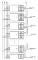
도 1은 본 개시의 제1 실시예에서 제공되는 시프트 레지스터 유닛의 구조의 개략도이다.
도 2는 본 개시의 제2 실시예에서 제공되는 다른 시프트 레지스터 유닛의 구조의 개략도이다.
도 3은 본 개시의 제3 실시예에서 제공되는, 도 1에 도시된 바와 같은 시프트 레지스터 유닛에 의해 이루어진 게이트 드라이버 회로의 구조의 개략도이다.
도 4는 본 개시의 제1 실시예에서 제공되는 시프트 레지스터 유닛의 개별 신호 단자들에서의 신호들의 타이밍도이다.
도 5는 본 개시의 제4 실시예에서 제공되는, 도 1에 도시된 바와 같은 시프트 레지스터 유닛에 의해 이루어진 게이트 드라이버 회로의 구조의 개략도이다.1 is a schematic view of the structure of a shift register unit provided in the first embodiment of the present disclosure;
2 is a schematic view of the structure of another shift register unit provided in the second embodiment of the present disclosure;
3 is a schematic diagram of the structure of a gate driver circuit made up of a shift register unit as shown in Fig. 1, which is provided in the third embodiment of the present disclosure.
4 is a timing diagram of signals at the individual signal terminals of the shift register unit provided in the first embodiment of the present disclosure;
5 is a schematic view of the structure of a gate driver circuit made up of a shift register unit as shown in Fig. 1, which is provided in the fourth embodiment of the present disclosure.
본 개시의 실시예들에서, 출력 단자가 풀다운되어야 하는 기간 동안 출력 단자가 풀다운되지 않는 시간 인터벌 및 임계 전압들에서의 드리프트에 의해 일어난 출력 오류들을 억제하도록 구성되어 시프트 레지스터 유닛의 안정성을 증가시키는 시프트 레지스터 유닛 및 게이트 드라이버 회로가 제공된다.In embodiments of the present disclosure, a shift that is configured to suppress output errors caused by drift at threshold voltages and time intervals during which the output terminal is not pulled down during the period during which the output terminal must be pulled down and shifts that increase the stability of the shift register unit A register unit and a gate driver circuit are provided.
이하, 첨부 도면을 참조하여 본 개시의 실시예들에 대한 설명이 주어질 것이다.Hereinafter, a description will be given of embodiments of the present disclosure with reference to the accompanying drawings.
본 개시의 제1 실시예에 제공되는 시프트 레지스터 유닛은 도 1에 도시된 바와 같은 구조를 갖는다. 시프트 레지스터 유닛은 입력 모듈(101), 제1 출력 모듈(102), 풀다운 구동 모듈(103), 풀다운 모듈(104), 및 제1 출력 방전 모듈(105)을 포함한다는 것을 도 1로부터 알 수 있다.The shift register unit provided in the first embodiment of the present disclosure has a structure as shown in Fig. It can be seen from FIG. 1 that the shift register unit includes an
입력 모듈(101)은 시프트 레지스터 유닛에서 입력 신호 단자 및 제1 클럭 신호 입력 단자에 연결되고, 입력 신호 및 제1 클럭 신호에 응답하여 풀업 노드에 입력 신호를 제공하도록 구성된다. 풀업 노드는 입력 모듈과 제1 출력 모듈 사이의 연결 지점이다.The
제1 출력 모듈(102)는 제2 클럭 신호 입력 단자에 연결되고, 풀업 노드에서의 전압 신호에 응답하여 시프트 레지스터 유닛에서의 제1 출력 단자에 제2 클럭 신호를 제공하도록 구성된다. The
풀다운 구동 모듈(103)은 제1 클럭 신호 입력 단자 및 제2 클럭 신호 입력 단자에 연결되고, 제1 클럭 신호에 응답하여 제1 클럭 신호를 제1 풀다운 노드에 제공하고, 제2 클럭 신호에 응답하여 제2 클럭 신호를 제2 풀다운 노드에 제공하고; 풀업 노드에서의 전압 신호에 응답하여 제1 풀다운 노드 및 제2 풀다운 노드에 제1 저전압 신호를 제공하고; 제1 풀다운 노드에서의 전압 신호에 응답하여 제1 저전압 신호를 제2 풀다운 노드에 제공하고; 그리고 제2 풀다운 노드에서의 전압 신호에 응답하여 제1 저전압 신호를 제1 풀다운 노드에 제공하도록 구성된다. 제1 풀다운 노드와 제2 풀다운 노드는 둘 다 풀다운 구동 모듈과 풀다운 모듈 사이의 연결 지점들이다.The pull-
풀다운 모듈(104)은 제1 풀다운 노드에서의 전압 신호 및 제2 풀다운 노드에서의 전압 신호에 응답하여 제1 저전압 신호를 풀업 노드에 제공하도록 구성된다.The pull down
제1 출력 방전 유닛(105)은 제1 풀다운 노드에서의 전압 신호 및 제2 풀다운 노드에서의 전압 신호에 응답하여 제2 저전압 신호를 시프트 레지스터 유닛의 제1 출력 단자에 제공하도록 구성된다.The first
본 실시예에서, 제1 저전압 신호는 제2 저전압 신호보다 작거나 같고, 제1 저전압 신호 및 제2 저전압 신호는 노드들 및/또는 이에 연결된 출력 단자들에서의 전위들을 풀다운하기 위해 모두 음의 전압들이다.In the present embodiment, the first undervoltage signal is less than or equal to the second undervoltage signal, and the first undervoltage signal and the second undervoltage signal are both negative voltages to pull down the potentials at the nodes and / admit.
본 개시의 동작 원리는 특정 실시예들을 참조하여 이하 상세히 설명될 것이다. 실시예들은 단지 본 개시의 더 나은 설명을 위한 것이고, 본 개시를 제한하지 않는다는 점에 유의해야 한다.The principles of operation of the present disclosure will be described in detail below with reference to specific embodiments. It should be noted that the embodiments are merely for a better description of the present disclosure and are not intended to limit the present disclosure.
도 1에 도시된 바와 같은 시프트 레지스터 유닛은 입력 모듈(101), 제1 출력 모듈(102), 풀다운 구동 모듈(103), 풀다운 모듈(104), 및 제1 출력 방전 모듈(105)을 포함한다.The shift register unit as shown in Fig. 1 includes an
구체적으로, 입력 모듈(101)은 시프트 레지스터 유닛의 입력 신호 단자(INPUT)에 연결된 게이트 및 소스, 및 제2 TFT(T2)의 소스에 연결된 드레인을 갖는 제1 박막 트랜지스터(TFT)(T1); 및 제1 클럭 신호(CK) 입력 단자에 연결된 게이트 및 풀업 노드(PU)에 연결된 드레인을 갖는 제2 TFT(T2)를 포함한다.Specifically, the
입력 신호는 풀업 노드(PU)에서의 전위를 증가시키기 위해 제1 TFT(T1) 및 제2 TFT(T2)를 통해 풀업 노드(PU)에 제공된다.An input signal is provided to the pull-up node (PU) through the first TFT (T1) and the second TFT (T2) to increase the potential at the pull-up node (PU).
제1 출력 모듈(102)은 풀업 노드(PU)에 연결된 게이트, 제2 클럭 신호(CKB) 입력 단자에 연결된 드레인, 및 제1 출력 단자(OT1)에 연결된 소스를 갖는 제3 TFT(T3); 및 풀업 노드(PU)와 제1 출력 단자(OT1) 사이에 연결되고, 풀업 노드(PU)에서의 전위를 유지하여 제3 TFT(T3)가 일정 기간 동안 계속 턴온되도록 구성된 커패시터(C)를 포함한다.The
풀다운 구동 모듈(103)은 제1 클럭 신호(CK) 입력 단자에 연결된 게이트 및 드레인, 및 제1 풀다운 노드(PD1)에 연결된 소스를 갖는 제4 TFT(T4); 제2 클럭 신호(CKB) 입력 단자에 동시에 연결된 게이트 및 소스, 및 제2 풀다운 노드(PD2)에 연결된 드레인을 갖는 제5 TFT(T5); 풀업 노드(PU)에 연결된 게이트, 제1 풀다운 노드(PD1)에 연결된 드레인, 및 제7 TFT(T7)의 드레인에 연결된 소스를 갖는 제6 TFT(T6); 풀업 노드(PU)에 연결된 게이트 및 제1 저전압 신호(Vgl_1) 입력 단자에 연결된 소스를 갖는 제7 TFT(T7); 풀업 노드(PU)에 연결된 게이트, 제2 풀다운 노드(PD2)에 연결된 드레인, 및 제9 TFT(T9)의 드레인에 연결된 소스를 갖는 제8 TFT(T8); 풀업 노드(PU)에 연결된 게이트 및 제1 저전압 신호(Vgl_1) 입력 단자에 연결된 소스를 갖는 제9 TFT(T9); 제2 풀다운 노드(PD2)에 연결된 게이트, 제1 풀다운 노드(PD1)에 연결된 드레인, 및 제1 저전압 신호(Vgl_1) 입력 단자에 연결된 소스를 갖는 제10 TFT(T10); 및 제1 풀다운 노드(PD1)에 연결된 게이트, 제2 풀다운 노드(PD2)에 연결된 소스, 및 제1 저전압 신호(Vgl_1) 입력 단자에 연결된 드레인을 갖는 제11 TFT(T11)를 포함한다. The pull-down driving module 103 includes a fourth TFT T4 having a gate and a drain connected to the first clock signal (CK) input terminal, and a source connected to the first pull-down node PD1; A fifth TFT (T5) having a gate and a source simultaneously connected to the second clock signal (CKB) input terminal, and a drain connected to the second pull-down node (PD2); A sixth TFT (T6) having a gate connected to the pull-up node (PU), a drain connected to the first pull-down node (PD1), and a source connected to the drain of the seventh TFT (T7); A seventh TFT (T7) having a gate connected to the pull-up node (PU) and a source connected to the first low voltage signal (Vgl_1) input terminal; An eighth TFT (T8) having a gate connected to the pull-up node (PU), a drain connected to the second pull-down node (PD2), and a source connected to the drain of the ninth TFT (T9); A ninth TFT (T9) having a gate connected to the pull-up node (PU) and a source connected to the first low voltage signal (Vgl_1) input terminal; A tenth TFT T10 having a gate connected to the second pull-down node PD2, a drain connected to the first pull-down node PD1, and a source connected to the first low-voltage signal Vgl_1 input terminal; And a tenth TFT T11 having a gate connected to the first pull-down node PD1, a source connected to the second pull-down node PD2, and a drain connected to the first low-voltage signal Vgl_1 input terminal.
풀다운 구동 모듈(103)은 제4 TFT(T4)를 통해 제1 풀다운 노드(PD1)를 충전하고, 제5 TFT(T5)를 통해 제2 풀다운 노드(PD2)를 충전하고, 제6 TFT(T6), 제7 TFT(T7), 및 제10 TFT(T10)를 통해 제1 풀다운 노드(PD1)를 방전하고, 제8 TFT(T8), 제9 TFT(T9), 및 제11 TFT(T11)를 통해 제2 풀다운 노드(PD2)를 방전한다. 제1 풀다운 노드(PD1)에서의 전위 및 제2 풀다운 노드(PD2)에서의 전위가 비-출력 국면 동안 AC 신호이기 때문에, 소자들의 임계 전압에서의 드리프트들에 의해 일어나는 출력 오류들은 효과적으로 억제될 수 있고, 이에 따라 노이즈 감소 효과가 증가할 수 있다. 제1 풀다운 노드(PD1)에서의 전압 신호와 제2 풀다운 노드(PD2)에서의 전압 신호가 상호 보완적이기 때문에, 제1 출력 방전 모듈(105)은 항상 비-출력 국면 동안 제1 출력 단자(OT1)를 방전하며, 이로써 출력 단자를 풀다운하는 동작에 존재하는 인터벌에 의해 일어나는 출력 오류를 제거한다.The pull-down
풀다운 모듈(104)은 제1 풀다운 노드(PD1)에 연결된 게이트, 풀업 노드(PU)에 연결된 소스, 및 제13 TFT(T13)의 드레인에 연결된 드레인을 갖는 제12 TFT(T12); 제1 풀다운 노드(PD1)에 연결된 게이트 및 제1 저전압 신호(Vgl_1) 입력 단자에 연결된 드레인을 갖는 제13 TFT(T13); 제2 풀다운 노드(PD2)에 연결된 게이트, 풀업 노드(PU)에 연결된 소스, 및 제15 TFT(T15)의 소스에 연결된 드레인을 갖는 제14 TFT(T14); 제2 풀다운 노드(PD2)에 연결된 게이트 및 제1 저전압 신호(Vgl_1) 입력 단자에 연결된 드레인을 갖는 제15 TFT(T15)를 포함한다.The pull-
풀다운 모듈(104)은 AC 신호들에 의해 일어나는 노이즈를 제거하기 위해 제1 풀다운 노드(PD1)에서의 전압 신호 및 제2 풀다운 노드(PD2)에서의 전압 신호에 응답하여 풀업 노드(PU)를 지속적으로 방전한다.Pull-
제1 출력 방전 모듈(105)은 제1 풀다운 노드(PD1)에 연결된 게이트, 제1 출력 단자(OT1)에 연결된 드레인, 및 제2 저전압 신호(Vgl_2) 입력 단자에 연결된 소스를 갖는 제16 TFT(T16); 및 제2 풀다운 노드(PD2)에 연결된 게이트, 제1 출력 단자(OT1)에 연결된 드레인, 및 제2 저전압 신호(Vgl_2) 입력 단자에 연결된 소스를 갖는 제17 TFT(T17)를 포함한다.The first
제1 출력 방전 모듈(105)은 제1 풀다운 노드(PD1)에서의 전압 신호 및 제2 풀다운 노드(PD2)에서의 전압 신호에 응답하여 비-출력 국면 동안 제1 출력 단자(OT1)를 지속적으로 방전하여, AC 신호들에 의해 일어나는 노이즈를 제거한다.The first
시프트 레지스터 유닛에서, 풀다운 구동 모듈(104)은 제1 클럭 신호(CK) 입력 단자 및 제2 클럭 신호(CKB) 입력 단자에 연결되고, 제1 클럭 신호(CK)에 응답하여 제1 클럭 신호(CK)를 제1 풀다운 노드(PD1)에 제공하고, 제2 클럭 신호(CKB)에 응답하여 제2 클럭 신호(CKB)를 제2 풀다운 노드(PD2)에 제공하고; 풀업 노드(PU)에서의 전압 신호에 응답하여 제1 풀다운 노드(PD1) 및 제2 풀다운 노드(PD2)에 제1 저전압 신호(Vgl_1)를 제공하고; 제1 풀다운 노드(PD1)에서의 전압 신호에 응답하여 제1 저전압 신호(Vgl_1)를 제2 풀다운 노드(PD2)에 제공하고; 그리고 제2 풀다운 노드(PD2)에서의 전압 신호에 응답하여 제1 저전압 신호(Vgl_1)를 제1 풀다운 노드(PD1)에 제공하도록 구성된다. 비-출력 국면 동안, 제1 풀다운 노드(PD1)에서의 전압 신호 및 제2 풀다운 노드(PD2)에서의 전압 신호는 소자들의 임계 전압들에서의 드리프트들에 의해 일어나는 출력 오류들을 효과적으로 억제하기 위해 모두 AC 신호들이다. 한편, 제1 풀다운 노드(PD1)에서의 전압 신호와 제2 풀다운 노드(PD2)에서의 전압 신호는 상호 보완적이어서 제1 출력 방전 모듈(105)은 항상 비-출력 국면 동안 제1 출력 단자(OT1)를 방전하며, 이로써 제1 출력 단자를 풀다운하는 동작에 존재하는 인터벌에 의해 일어나는 출력 오류를 제거한다.In the shift register unit, the pull-down
시프트 레지스터 유닛에서, 제6 TFT(T6)의 소스와 제8 TFT(T8)의 소스에 동시에 연결된 리셋 신호 입력 단자(RESET)가 또한 존재한다. 리셋 신호가 고레벨인 경우, 제6 TFT(T6) 및 제8 TFT(T8)의 소스들은 또한 고레벨이며, 이로써 제6 TFT(T6) 및 제8 TFT(T8)는 신속히 턴오프되어 암전류(dark current)가 제8 TFT(T8)를 통해 흐르는 것을 방지하여 제2 풀다운 노드(PD2)를 방전하면서, 암전류가 제6 TFT(T6)를 통해 흐르는 것을 방지하여 제1 풀다운 노드(PD1)를 방전한다.In the shift register unit, there is also a reset signal input terminal RESET simultaneously connected to the source of the sixth TFT T6 and the source of the eighth TFT T8. The source of the sixth TFT T6 and the source of the eighth TFT T8 are also at a high level so that the sixth TFT T6 and the eighth TFT T8 are quickly turned off so that the dark current Is prevented from flowing through the eighth TFT T8 to discharge the second pull-down node PD2 while preventing the dark current from flowing through the sixth TFT T6, thereby discharging the first pull-down node PD1.
제1 저전압 신호(Vgl_1)는 제2 저전압 신호(Vgl_2)보다 작으며, 이로써 제16 TFT(T16) 및 제17 TFT(T17)가 훨씬 더 쉽게 턴오프되어 암전류가 제16 TFT(T16) 및 제17 TFT(T17)를 통해 흐르는 것을 효과적으로 방지하여 출력 국면 동안 제1 출력 단자(OT1)를 방전한다.The first low voltage signal Vgl_1 is smaller than the second low voltage signal Vgl_2 so that the sixteenth TFT T16 and the seventeenth TFT T17 are much more easily turned off so that the dark current flows through the sixteenth TFTs T16, 17 TFT (T17) to discharge the first output terminal OT1 during the output phase.
도 2는 본 개시의 제2 실시예에서 제공되는 시프트 레지스터 유닛을 도시한다. 도 2를 참조하면, 여기에 도시된 시프트 레지스트 유닛은 입력 모듈(101), 제1 출력 모듈(102), 풀다운 구동 모듈(103), 풀다운 모듈(104), 및 제1 출력 방전 모듈(105)을 포함할 뿐 아니라, 제2 출력 모듈(106), 제2 출력 방전 모듈(107), 제3 출력 모듈(108), 제3 출력 방전 모듈(109), 및 피드백 모듈(110)을 포함한다.Figure 2 shows the shift register unit provided in the second embodiment of the present disclosure. 2, the shift resist unit shown here includes an
제2 실시예에서, 제2 출력 모듈(106)은 제2 클럭 신호(CKB) 입력 단자에 연결되고, 시프트 레지스터 유닛보다 일 스테이지 이전의 다른 시프트 레지스터 유닛에 리셋 신호를 제공하기 위해 풀업 노드(PU)에서의 전압 신호에 응답하여 제2 클럭 신호(CKB)를 제2 출력 단자(OT2)에 제공하도록 구성된다.In the second embodiment, the
여기에서, 제2 출력 모듈(106)은 풀업 노드(PU)에 연결된 게이트, 제2 클럭 신호(CKB) 입력 단자에 연결된 드레인, 및 제2 출력 단자(OT2)에 연결된 소스를 갖는 제18 TFT(T18)를 포함한다.Here, the
제2 출력 방전 모듈(107)은 제1 풀다운 노드(PD1)에서의 전압 신호 및 제2 풀다운 노드(PD2)에서의 전압 신호에 응답하여 제2 저전압 신호(Vgl_2)를 제2 출력 단자(OT2)에 제공하도록 구성된다.The second
여기에서, 제2 출력 방전 모듈(107)은 제1 풀다운 노드(PD1)에 연결된 게이트, 제2 출력 단자(OT2)에 연결된 드레인, 및 제2 저전압 신호(Vgl_2) 입력 단자에 연결된 소스를 갖는 제19 TFT(T19); 및 제2 풀다운 노드(PD2)에 연결된 게이트, 제2 출력 단자(OT2)에 연결된 드레인, 및 제2 저전압 신호(Vgl_2) 입력 단자에 연결된 소스를 갖는 제20 TFT(T20)를 포함한다.Here, the second
제2 출력 방전 모듈(107)은 제1 풀다운 노드(PD1)에서의 전압 신호 및 제2 풀다운 노드(PD2)에서의 전압 신호에 응답하여 비-출력 국면 동안 제2 출력 단자(OT2)를 지속적으로 방전하여, AC 신호들에 의해 일어나는 노이즈를 제거한다.The second
제3 출력 모듈(108)은 제2 클럭 신호(CKB) 입력 단자에 연결되고, 시프트 레지스터 유닛보다 일 스테이지 다음의 다른 시프트 레지스터 유닛에 시작 신호를 제공하기 위해 풀업 노드(PU)에서의 전압 신호에 응답하여 제2 클럭 신호(CKB)를 제3 출력 단자(OT3)에 제공하도록 구성된다.The
여기에서, 제3 출력 모듈(108)은 풀업 노드(PU)에 연결된 게이트, 제2 클럭 신호(CKB) 입력 단자에 연결된 드레인, 및 제3 출력 단자(OT3)에 연결된 소스를 갖는 제21 TFT(T21)를 포함한다.Here, the
제3 출력 방전 모듈(109)은 시프트 레지스터 유닛보다 일 스테이지 다음의 다른 시프트 레지스터 유닛에 시작 신호를 제공하기 위해, 제1 풀다운 노드(PD1)에서의 전압 신호 및 제2 풀다운 노드(PD2)에서의 전압 신호에 응답하여 제1 저전압 신호(Vgl_1)를 제3 출력 단자(OT3)에 제공하도록 구성된다.The third
여기에서, 제3 출력 방전 모듈(109)은 제1 풀다운 노드(PD1)에 연결된 게이트, 제3 출력 단자(OT3)에 연결된 드레인, 및 제1 저전압 신호(Vgl_1) 입력 단자에 연결된 소스를 갖는 제22 TFT(T22); 및 제2 풀다운 노드(PD2)에 연결된 게이트, 제3 출력 단자(OT3)에 연결된 드레인, 및 제1 저전압 신호(Vgl_1) 입력 단자에 연결된 소스를 갖는 제23 TFT(T23)를 포함한다.Here, the third
제3 출력 방전 모듈(109)은 제1 풀다운 노드(PD1)에서의 전압 신호 및 제2 풀다운 노드(PD2)에서의 전압 신호에 응답하여 비-출력 국면 동안 제3 출력 단자(OT3)를 지속적으로 방전하여, AC 신호들에 의해 일어나는 노이즈를 제거한다.The third
피드백 모듈(110)은 제3 출력 단자(OT3)에서의 전압 신호에 응답하여 입력 모듈(101) 및 풀다운 모듈(104)에 제2 출력 단자(OT2)에서의 전압 신호를 제공하도록 구성된다.The
여기에서, 피드백 모듈(110)은 제3 출력 단자(OT3)에 연결된 게이트, 제1 TFT(T1)의 드레인, 제12 TFT(T12)의 드레인, 및 제14 TFT(T14)의 드레인에 연결된 드레인, 및 제2 출력 단자(OT2)에 연결된 소스를 갖는 제24 TFT(T24)를 포함한다.Here, the
제2 출력 단자(OT2)에서의 출력이 고레벨인 경우, 제2 TFT(T2)의 소스, 제13 TFT(T13)의 소스, 및 제15 TFT(T15)의 소스는 모두 고레벨이며, 이로써 제2 TFT(T2), 제13 TFT(T13), 및 제15 TFT(T15)는 모두 턴오프되고, 이 때 제1 TFT(T1), 제12 TFT(T12), 및 제14 TFT(T14)는 또한 완전히 턴오프되며, 이로써 암전류가 제2 TFT(T2), 제12 TFT(T12), 및 제14 TFT(T14)에서 발생되는 것을 방지하여 풀업 노드(PU)를 방전한다. The source of the second TFT T2, the source of the thirteenth TFT T13 and the source of the fifteenth TFT T15 are all at a high level when the output from the second output terminal OT2 is at a high level, The TFT T2, the thirteenth TFT T13 and the fifteenth TFT T15 are both turned off and the first TFT T1, the twelfth TFT T12 and the fourteenth TFT T14 are also turned off Thereby completely discharging the pull-up node PU by preventing the dark current from being generated in the second TFT T2, the twelfth TFT T12, and the fourteenth TFT T14.
커패시터(C)가 풀업 노드(PU)와 제1 출력 단자(OT1) 사이에 설정되거나, 풀업 노드(PU)와 제2 출력 단자(OT2) 사이에 설정되거나, 풀업 노드(PU)와 제3 출력 단자(OT3) 사이에 설정될 수도 있다는 점에 주목해야 한다. 이들 3개의 연결 방식에서, 커패시터의 기능은 풀업 노드(PU)에서의 전위를 유지하는 것과 동일하다.In which the capacitor C is set between the pull-up node PU and the first output terminal OT1 or between the pull-up node PU and the second output terminal OT2 or between the pull-up node PU and the third output Terminal OT3, as shown in Fig. In these three connection schemes, the function of the capacitor is the same as maintaining the potential at the pull-up node (PU).
전술한 TFT들 중 어느 하나에서, 화살표를 갖는 하나의 전극은 TFT의 소스이고, 화살표의 방향은 TFT에서의 전류 방향이다.In any one of the above-described TFTs, one electrode with an arrow is the source of the TFT, and the direction of the arrow is the current direction in the TFT.
본 개시의 제2 실시예에 제공되는 시프트 레지스터 유닛에서, 시프트 레지스터 유닛의 특정 스테이지의 출력에서의 오류는 시프트 레지스터 유닛보다 일 스테이지 이전의 다른 시프트 레지스터 유닛들 및 시프트 레지스터 유닛보다 일 스테이지 다음의 다른 시프트 레지스터 유닛들의 동작 상태들에 영향을 미치지 않는데, 그 이유는 리셋 신호 및 시작 신호가 별도의 회로들을 통해 출력되기 때문이다. In the shift register unit provided in the second embodiment of the present disclosure, an error at the output of the specific stage of the shift register unit is detected by comparing the shift register unit with the other shift register units before the one shift register unit Does not affect the operational states of the shift register units because the reset signal and the start signal are output via separate circuits.
전술한 시프트 레지스터 유닛들이 캐스케이드로 연결되어 어레이 기판 상의 게이트 드라이버 회로를 형성한다. 본 개시의 실시예들에서 제공되는 게이트 드라이버 회로는 캐스케이드로 연결된 시프트 레지스터 유닛들의 개별 스테이지들을 포함하는데, 시프트 레지스터 유닛의 제1 스테이지의 입력 신호 단자는 게이트 드라이버 회로의 시작 신호 단자에 연결되고, 시프트 레지스터 유닛의 제1 스테이지의 리셋 신호 단자는 시프트 레지스터 유닛의 제2 스테이지의 출력 단자들 중 어느 하나에 연결되고, 시프트 레지스터 유닛의 최종 스테이지의 입력 신호 단자는 시프트 레지스터 유닛의 이전 스테이지의 출력 단자들 중 어느 하나에 연결되고, 시프트 레지스터 유닛의 최종 스테이지의 리셋 신호 단자는 시작 신호 단자에 연결된다. 시프트 레지스터 유닛들의 제1 스테이지와 최종 스테이지를 제외하고, 시프트 레지스터 유닛들의 나머지 스테이지 각각의 입력 신호 단자는 시프트 레지스터 유닛의 이전 스테이지의 출력 단자들 중 어느 하나에 연결되고, 시프트 레지스터 유닛들의 나머지 스테이지 각각의 리셋 신호 단자는 시프트 레지스터 유닛의 다음 스테이지의 출력 단자들 중 어느 하나에 연결된다. 전술한 캐스케이드로 연결된 시프트 레지스터 유닛들 각각은 도 1에 도시된 바와 같은 시프트 레지스터 유닛 또는 도 2에 도시된 바와 같은 시프트 레지스터 유닛이다.The aforementioned shift register units are cascaded to form the gate driver circuit on the array substrate. The gate driver circuit provided in the embodiments of the present disclosure includes individual stages of cascade-connected shift register units, wherein the input signal terminal of the first stage of the shift register unit is connected to the start signal terminal of the gate driver circuit, The reset signal terminal of the first stage of the register unit is connected to one of the output terminals of the second stage of the shift register unit and the input signal terminal of the last stage of the shift register unit is connected to the output terminals of the previous stage of the shift register unit And the reset signal terminal of the last stage of the shift register unit is connected to the start signal terminal. The input signal terminals of each of the remaining stages of the shift register units, except for the first stage and the last stage of the shift register units, are connected to one of the output terminals of the previous stage of the shift register unit, The reset signal terminal of the shift register unit is connected to one of the output terminals of the next stage of the shift register unit. Each of the aforementioned cascade-connected shift register units is a shift register unit as shown in Fig. 1 or a shift register unit as shown in Fig.
구체적으로, 어레이 기판 상의 게이트 드라이버 회로는 시프트 레지스터 유닛들의 N개의 스테이지들을 포함하는데, N은 게이트 라인들의 개수이고, 시작 신호(STV)는 입력 신호로서 시프트 레지스터 유닛의 제1 스테이지에 입력되고, 게이트 구동 신호들은 개별 게이트 라인들에 순차적으로 출력되고, 시프트 레지스터 유닛의 n번째 스테이지의 입력 신호는 시프트 레지스터 유닛의 (n-1)번째 스테이지의 출력 신호에 의해 공급되고, 시프트 레지스터 유닛의 n번째 스테이지의 리셋 신호는 시프트 레지스터 유닛의 (n+1)번째 스테이지의 출력 신호에 의해 공급되는데, 여기서 n<N이다.Specifically, the gate driver circuit on the array substrate includes N stages of shift register units, where N is the number of gate lines, the start signal STV is input to the first stage of the shift register unit as an input signal, The driving signals are sequentially output to the individual gate lines, and the input signal of the n-th stage of the shift register unit is supplied by the output signal of the (n-1) -th stage of the shift register unit, Is supplied by the output signal of the (n + 1) < th > stage of the shift register unit, where n <
도 3은 본 개시의 제3 실시예에서 제공되는 바와 같이 캐스케이드로 연결된 도 1에 도시된 바와 같은 시프트 레지스터 유닛들에 의해 형성된 어레이 기판 상의 게이트 드라이버 회로를 도시한다. 도 4는 시프트 레지스터 유닛에서 개별 신호 단자들에서의 신호들의 타이밍도이다. 이하, 어레이 기판 상의 게이트 드라이버 회로에서 시프트 레지스터 유닛의 n번째 스테이지의 동작 방법은 도 4를 참조하여 설명될 것이며, 여기서 n<N이고, N은 어레이 기판 상의 게이트 드라이버 회로에서 시프트 레지스터 유닛들의 스테이지들의 개수이다.Figure 3 shows a gate driver circuit on an array substrate formed by shift register units as shown in Figure 1 cascaded as provided in the third embodiment of the present disclosure. 4 is a timing diagram of signals at individual signal terminals in the shift register unit. Hereinafter, a method of operating the nth stage of the shift register unit in the gate driver circuit on the array substrate will be described with reference to Fig. 4, where n < N and N is the number of stages of the shift register units in the gate driver circuit on the array substrate The number.
게이트 드라이버 회로가 스캐닝 동작을 수행하는 경우, 게이트 드라이버 회로 내의 TFT들의 전부는 고레벨에서 턴온되고, 저레벨에서 턴오프된다. 제1 클럭 신호(CK) 및 제2 클럭 신호(CKB)는 서로 상반되는 국면들을 갖는다.When the gate driver circuit performs the scanning operation, all of the TFTs in the gate driver circuit are turned on at the high level and turned off at the low level. The first clock signal CK and the second clock signal CKB have opposite phases.
제1 국면(S1) 동안, 제1 클럭 신호(CK)는 저레벨이고, 제2 클럭 신호(CKB)는 고레벨인데, 시프트 레지스터 유닛의 n번째 스테이지의 입력 신호인 시프트 레지스터 유닛의 (n-1)번째 스테이지의 출력 신호(OUTPUT(n-1))는 저레벨에 있고, 시프트 레지스터 유닛의 n번째 스테이지의 리셋 신호인 시프트 레지스터의 (n+1)번째 스테이지의 출력 신호(OUTPUT(n+1))는 저레벨에 있고, 제1 풀다운 노드(PD1)는 저레벨에 있고, 제2 풀다운 노드(PD2)는 고레벨에 있다.During the first phase S1, the first clock signal CK is at a low level and the second clock signal CKB is at a high level. The (n-1) th shift register unit, which is the nth stage input signal of the shift register unit, The output signal OUTPUT (n + 1) of the (n + 1) -th stage of the shift register, which is the reset signal of the n-th stage of the shift register unit, The first pull-down node PD1 is at a low level, and the second pull-down node PD2 is at a high level.
제10 TFT(T10), 제14 TFT(T14), 제15 TFT(T15), 및 제17 TFT(T17)은 제2 풀다운 노드(PD2)에서의 고레벨 전압 신호에 응답하여 턴온되고, 제14 TFT(T14) 및 제15 TFT(T15)는 제1 저전압 신호(Vg1_1)를 풀업 노드(PU)에 제공하고, 제10 TFT(T10)는 제1 저전압 신호(Vg1_1)를 제1 풀다운 노드(PD1)에 제공하고, 제17 TFT(T17)는 제2 저전압 신호(Vg1_2)를 제1 출력 단자(OT1)에 제공한다.The tenth TFT T10, the fourteenth TFT T14, the fifteenth TFT T15 and the seventeenth TFT T17 are turned on in response to the high level voltage signal at the second pull-down node PD2, The first TFT T14 and the fifteenth TFT T15 provide the first low voltage signal Vg1_1 to the pull-up node PU and the tenth TFT T10 supplies the first low voltage signal Vg1_1 to the first pull- And the seventeenth TFT T17 supplies the second low voltage signal Vg1_2 to the first output terminal OT1.
그러므로, 제1 출력 단자(OT1)에서의 출력 신호(OUTPUT(n))는 이 경우 저레벨에 있다.Therefore, the output signal OUTPUT (n) at the first output terminal OT1 is at the low level in this case.
제2 국면(S2) 동안, 제1 클럭 신호(CK)는 고레벨에 있고, 제2 클럭 신호(CKB)는 저레벨에 있고, OUTPUT(n-1)는 고레벨에 있고, OUTPUT(n+1)는 저레벨에 있다.During the second phase S2, the first clock signal CK is at a high level, the second clock signal CKB is at a low level, OUTPUT (n-1) is at a high level, and OUTPUT (n + It is at a low level.
입력 신호(OUTPUT(n-1))가 고레벨에 있기 때문에 제1 TFT(T1)는 턴온되고, 제1 클럭 신호(CK)가 고레벨에 있기 때문에 제2 TFT(T2)는 턴온되고, 입력 신호는 제1 TFT(T1) 및 제2 TFT(T2)를 통해 커패시터(C)를 충전하고, 풀업 노드(PU)는 고레벨이다. 이 때에, 제3 TFT(T3)는 풀업 노드(PU)에서의 전압 신호에 응답하여 턴온되지만, 제2 클럭 신호(CKB)가 저레벨에 있기 때문에 제1 출력 단자(OT1)에서의 출력 신호(OUTPUT(n))는 저레벨에 있다.The first TFT T1 is turned on because the input signal OUTPUT (n-1) is at a high level and the second TFT T2 is turned on because the first clock signal CK is at a high level, The capacitor C is charged through the first TFT T1 and the second TFT T2 and the pull-up node PU is at a high level. At this time, since the third TFT T3 is turned on in response to the voltage signal at the pull-up node PU but the second clock signal CKB is at the low level, the output signal OUTPUT (n) is at a low level.
한편, 제6 TFT(T6), 제7 TFT(T7), 제8 TFT(T8), 및 제9 TFT(T9)는 풀업 노드(PU)에서의 전압 신호에 응답하여 턴온되고, 제1 풀다운 노드(PD1)는 제6 TFT(T6) 및 제7 TFT(T7)를 통해 지속적으로 방전되어 저레벨로 유지하고, 제2 풀다운 노드(PD2)는 제8 TFT(T8) 및 제9 TFT(T9)를 통해 방전되고, 제2 풀다운 노드(PD2)에서의 전위가 신속히 감소한다.On the other hand, the sixth TFT T6, the seventh TFT T7, the eighth TFT T8 and the ninth TFT T9 are turned on in response to the voltage signal at the pull-up node PU, The first pull-down transistor PD1 is continuously discharged through the sixth TFT T6 and the seventh TFT T7 to be held at the low level and the second pull-down node PD2 is connected to the eighth TFT T8 and the ninth TFT T9 And the potential at the second pull-down node PD2 is rapidly reduced.
제3 국면(S3) 동안, 제1 클럭 신호(CK)는 저레벨에 있고, 제2 클럭 신호(CKB)는 고레벨에 있고, OUTPUT(n-1)는 저레벨에 있고, OUTPUT(n+1)는 저레벨에 있다.During the third phase S3, the first clock signal CK is at a low level, the second clock signal CKB is at a high level, OUTPUT (n-1) is at a low level, and OUTPUT It is at a low level.
입력 신호(OUTPUT(n-1))가 저레벨에 있기 때문에 제1 TFT(T1)는 턴오프되고, 제1 클럭 신호(CK)가 저레벨에 있기 때문에 제2 TFT(T2)는 턴오프되지만, 풀업 노드(PU)는 커패시터(C)로 인해 고레벨로 유지된다. 한편, 제2 클럭 신호(CKB)는 고레벨에 있고, 풀업 노드(PU)에서의 전위는 커패시터(C)의 부트스트래핑 기능(bootstrapping function)으로 인해 지속적으로 증가하며, 그 결과 제3 TFT(T3)는 턴온된 채로 유지된다.The first TFT T1 is turned off because the input signal OUTPUT (n-1) is at the low level and the second TFT T2 is turned off because the first clock signal CK is at the low level, The node PU is held at a high level due to the capacitor C. [ On the other hand, the second clock signal CKB is at a high level, and the potential at the pull-up node PU continuously increases due to the bootstrapping function of the capacitor C. As a result, the third TFT T3, Is kept turned on.
한편, 제6 TFT(T6), 제7 TFT(T7), 제8 TFT(T8), 및 제9 TFT(T9)는 풀업 노드(PU)에서의 전압 신호에 응답하여 턴온된 채로 유지되고, 제1 풀다운 노드(PD1) 및 제2 풀다운 노드(PD2)는 저레벨에 있다. 이 때에, 제16 TFT(T16)는 제1 풀다운 노드(PD1)에서의 저레벨 전압 신호에 응답하여 턴오프되고, 제17 TFT(T17)는 제2 풀다운 노드(PD2)에서의 고레벨 전압 신호에 응답하여 턴오프된다.On the other hand, the sixth TFT T6, the seventh TFT T7, the eighth TFT T8, and the ninth TFT T9 are kept turned on in response to the voltage signal at the pull-up node PU, 1 pull-down node PD1 and the second pull-down node PD2 are at a low level. At this time, the sixteenth TFT T16 is turned off in response to the low level voltage signal at the first pull-down node PD1, and the seventeenth TFT T17 is turned off in response to the high level voltage signal at the second pull- And is turned off.
그러므로, 제1 출력 단자(OT1)에서의 출력 신호(OUTPUT(n))는 고레벨이다.Therefore, the output signal OUTPUT (n) at the first output terminal OT1 is at a high level.
제4 국면(S4) 동안, 제1 클럭 신호(CK)는 고레벨에 있고, 제2 클럭 신호(CKB)는 저레벨에 있고, OUTPUT(n-1)는 저레벨에 있고, OUTPUT(n+1)는 고레벨에 있다.During the fourth phase S4, the first clock signal CK is at a high level, the second clock signal CKB is at a low level, OUTPUT (n-1) is at a low level, and OUTPUT It is at a high level.
OUTPUT(n+1)가 고레벨에 있기 때문에, 제6 TFT(T6), 제7 TFT(T7), 제8 TFT(T8), 및 제9 TFT(T9)는 완전히 턴오프된다. 제1 클럭 신호(CK)가 고레벨에 있어서 제1 클럭 신호(CK)를 제1 풀다운 노드(PD1)에 제공하기 때문에 제4 TFT(T4)는 턴온되고, 제1 풀다운 노드(PD1)는 고레벨로 증가한다. 제11 TFT(T11), 제12 TFT(T12), 제13 TFT(T13), 및 제16 TFT(T16)는 제1 풀다운 노드(PD1)에서의 고레벨 전압 신호에 응답하여 턴온되고, 제12 TFT(T12) 및 제13 TFT(T13)는 풀업 노드(PU)를 방전하고, 풀업 노드(PU)는 저레벨로 신속히 감소하고; 제11 TFT(T11)는 제1 저전압 신호(Vg1_1)를 제2 풀다운 노드(PD2)에 제공하고, 제2 풀다운 노드(PD2)는 저레벨로 유지되고; 제16 TFT(T16)는 제2 저전압 신호(Vg1_2)를 제1 출력 단자(OT1)에 제공한다.The sixth TFT T6, the seventh TFT T7, the eighth TFT T8, and the ninth TFT T9 are completely turned off because OUTPUT (n + 1) is at a high level. The fourth TFT T4 is turned on because the first clock signal CK is at the high level and the first clock signal CK is supplied to the first pull-down node PD1 and the first pull-down node PD1 is turned to the high level . The eleventh TFT T11, the twelfth TFT T12, the thirteenth TFT T13 and the sixteenth TFT T16 are turned on in response to the high level voltage signal at the first pull-down node PD1, The pull-up node T12 and the thirteenth TFT T13 discharge the pull-up node PU, and the pull-up node PU rapidly decreases to the low level; The eleventh TFT T11 supplies the first low voltage signal Vg1_1 to the second pull-down node PD2, and the second pull-down node PD2 is held at the low level; The sixteenth TFT T16 provides the second low voltage signal Vg1_2 to the first output terminal OT1.
그러므로, 제1 출력 단자(OT1)에서의 출력 신호(OUTPUT(n))는 이 때에 저레벨에 있다.Therefore, the output signal OUTPUT (n) at the first output terminal OT1 is at the low level at this time.
제5 국면(S5) 동안, 제1 클럭 신호(CK)는 저레벨에 있고, 제2 클럭 신호(CKB)는 고레벨에 있고, OUTPUT(n-1)는 저레벨에 있고, OUTPUT(n+1)는 저레벨에 있다.During the fifth phase S5, the first clock signal CK is at a low level, the second clock signal CKB is at a high level, OUTPUT (n-1) is at a low level, and OUTPUT (n + It is at a low level.
제2 클럭 신호(CKB)가 고레벨에 있기 때문에 제5 TFT(T5)는 턴온되고, 제8 TFT(T8) 및 제9 TFT(T9)는 풀업 노드(PU)에서의 전압 신호에 응답하여 턴오프된 채로 유지되고, 제2 풀다운 노드(PD2)는 고레벨로 증가하고, 제10 TFT(T10), 제14 TFT(T14), 제15 TFT(T15), 및 제17 TFT(T17)는 제2 풀다운 노드(PD2)에서의 고레벨 전압 신호에 응답하여 턴온되고, 제10 TFT(T10)는 제1 저전압 신호(Vg1_1)를 제1 풀다운 노드(PD1)에 제공하고, 제1 풀다운 노드(PD1)는 저레벨로 유지되고; 제14 TFT(T14) 및 제15 TFT(T15)는 풀업 노드(PU)를 지속적으로 방전하고, 풀업 노드(PU)는 저레벨로 유지되어 제3 TFT(T3)가 턴오프되고; 한편 제17 TFT(T17)는 제2 저전압 신호(Vg1_2)를 제1 출력 단자(OT1)에 제공한다.The fifth TFT T5 is turned on because the second clock signal CKB is at a high level and the eighth TFT T8 and the ninth TFT T9 are turned off in response to the voltage signal at the pull- The fourth pull-down node PD2 is maintained at the second pull-down node PD2 and the tenth TFT T10, the fourteenth TFT T14, the fifteenth TFT T15 and the seventeenth TFT T17 are kept at the high level, The first pull-down node PD1 is turned on in response to the high level voltage signal at the node PD2 and the tenth TFT T10 provides the first low voltage signal Vg1_1 to the first pull-down node PD1, / RTI > The fourteenth TFT T14 and the fifteenth TFT T15 continuously discharge the pull-up node PU and the pull-up node PU is held at low level to turn off the third TFT T3; On the other hand, the seventeenth TFT (T17) provides the second low voltage signal (Vg1_2) to the first output terminal (OT1).
그러므로, 제1 출력 단자(OT1)에서의 출력 신호(OUTPUT(n))는 저레벨에 있다.Therefore, the output signal OUTPUT (n) at the first output terminal OT1 is at the low level.
도 5는 본 개시의 제4 실시예에서 제공되는, 도 1에 도시된 바와 같은 시프트 레지스터 유닛에 의해 구성되는 어레이 기판 상의 게이트 드라이버 회로를 도시한다. 도 5를 참조하면, 게이트 드라이버 회로에서, 시프트 레지스터 유닛의 n번째 스테이지의 제1 출력 단자(OT1(n))는 현재 행에 대해 신호를 제공하고, 시프트 레지스터 유닛의 n번째 스테이지의 제2 출력 단자(OT2(n))는 시프트 레지스터 유닛의 (n-1)번째 스테이지에 리셋 신호를 제공하고, 시프트 레지스터 유닛의 n번째 스테이지의 제3 출력 단자(OT3(n))는 시프트 레지스터 유닛의 (n+1)번째 스테이지에 시작 신호를 제공한다. 제1 출력 단자(OT1(n)), 제2 출력 단자(OT2(n)), 및 제3 출력 단자(OT3(n))는 동일한 출력 신호인 OUTPUT(n)을 갖는다.Fig. 5 shows a gate driver circuit on an array substrate constituted by a shift register unit as shown in Fig. 1, which is provided in the fourth embodiment of the present disclosure. 5, in the gate driver circuit, the first output terminal OT1 (n) of the nth stage of the shift register unit provides a signal for the current row, and the second output terminal OT1 (n) of the nth stage of the shift register unit (N-1) th stage of the shift register unit, and the third output terminal OT3 (n) of the nth stage of the shift register unit supplies the reset signal to the (n-1) th stage of the shift register unit. n + 1) < th > stage. The first output terminal OT1 (n), the second output terminal OT2 (n), and the third output terminal OT3 (n) have the same output signal OUTPUT (n).
본 개시의 제4 실시예에서 제공되는 바와 같은 어레이 기판 상의 게이트 드라이버 회로에서의 시프트 레지스터 유닛의 n번째 스테이지의 동작 방법은 이하의 도 4를 참조하여 설명될 것이며, 여기서 n<N이고, N은 어레이 기판 상의 게이트 드라이버 회로에서 시프트 레지스터 유닛들의 스테이지들의 개수이다.The operation method of the n-th stage of the shift register unit in the gate driver circuit on the array substrate as provided in the fourth embodiment of the present disclosure will be described below with reference to Fig. 4, where n & Is the number of stages of shift register units in the gate driver circuit on the array substrate.
제1 국면(S1) 동안, 제1 클럭 신호(CK)는 저레벨이고, 제2 클럭 신호(CKB)는 고레벨에 있는데, 시프트 레지스터 유닛의 n번째 스테이지의 입력 신호인 시프트 레지스터 유닛의 (n-1)번째 스테이지의 출력 신호(OUTPUT(n-1))는 저레벨에 있고, 시프트 레지스터 유닛의 n번째 스테이지의 리셋 신호인 시프트 레지스터의 (n+1)번째 스테이지의 출력 신호(OUTPUT(n+1))는 저레벨에 있고, 제1 풀다운 노드(PD1)는 저레벨에 있고, 제2 풀다운 노드(PD2)는 고레벨에 있다.During the first phase S1, the first clock signal CK is at a low level and the second clock signal CKB is at a high level. The (n-1) th shift register unit of the shift register unit, which is the nth stage input signal of the shift register unit, (N + 1) -th stage output signal OUTPUT (n-1) of the shift register, which is the reset signal of the n-th stage of the shift register unit, Is at a low level, the first pull-down node PD1 is at a low level, and the second pull-down node PD2 is at a high level.
제10 TFT(T10), 제14 TFT(T14), 제15 TFT(T15), 및 제17 TFT(T17)는 제2 풀다운 노드(PD2)에서의 고레벨 전압 신호에 응답하여 턴온된다. 여기에서, 제10 TFT(T10)는 제1 저전압 신호(Vg1_1)를 제1 풀다운 노드(PD1)에 제공하고; 제14 TFT(T14) 및 제15 TFT(T15)는 제1 저전압 신호(Vg1_1)를 풀업 노드(PU)에 제공하고, 제3 TFT(T3), 제18 TFT(T18), 및 제21 TFT(T21)는 풀업 노드(PU)에서의 전압 신호에 응답하여 턴오프되고; 그리고 제17 TFT(T17)는 제2 저전압 신호(Vg1_2)를 제1 출력 단자(OT1(n))에 제공하고, 제20 TFT(T20)는 제2 저전압 신호(Vg1_2)를 제2 출력 단자(OT2(n))에 제공하고, 그리고 제23 TFT(T23)는 제1 저전압 신호(Vg1_1)를 제3 출력 단자(OT3(n))에 제공한다.The tenth TFT T10, the fourteenth TFT T14, the fifteenth TFT T15 and the seventeenth TFT T17 are turned on in response to the high level voltage signal at the second pull-down node PD2. Here, the tenth TFT T10 supplies the first low voltage signal Vg1_1 to the first pull-down node PD1; The fourteenth TFT T14 and the fifteenth TFT T15 provide the first low voltage signal Vg1_1 to the pull-up node PU and the third TFT T3, the eighteenth TFT T18, T21 is turned off in response to the voltage signal at the pull-up node PU; The seventeenth TFT T17 supplies the second low voltage signal Vg1_2 to the first output terminal OT1 (n) and the twentieth TFT T20 supplies the second low voltage signal Vg1_2 to the second output terminal OT1 OT2 (n), and the twenty-third TFT T23 provides the first low-voltage signal Vg1_1 to the third output terminal OT3 (n).
그러므로, 이 때에, 제1 출력 단자(OT1(n))에서의 출력 신호(OUTPUT(n)), 제2 출력 단자(OT2(n))에서의 출력 신호(OUTPUT(n)), 및 제3 출력 단자(OT3(n))에서의 출력 신호(OUTPUT(n))는 모두 저레벨에 있다.Therefore, at this time, the output signal OUTPUT (n) at the first output terminal OT1 (n), the output signal OUTPUT (n) at the second output terminal OT2 And the output signal OUTPUT (n) at the output terminal OT3 (n) are all at the low level.
제2 국면(S2) 동안, 제1 클럭 신호(CK)는 고레벨에 있고, 제2 클럭 신호(CKB)는 저레벨에 있고, OUTPUT(n-1)는 고레벨에 있고, OUTPUT(n+1)는 저레벨에 있다.During the second phase S2, the first clock signal CK is at a high level, the second clock signal CKB is at a low level, OUTPUT (n-1) is at a high level, and OUTPUT (n + It is at a low level.
입력 신호(OUTPUT(n-1))가 고레벨에 있기 때문에 제1 TFT(T1)는 턴온되고, 제1 클럭 신호(CK)가 고레벨에 있기 때문에 제2 TFT(T2)는 턴온되고, 입력 신호는 제1 TFT(T1) 및 제2 TFT(T2)를 통해 커패시터(C)를 충전하고, 이로써 풀업 노드(PU)는 고레벨에 있다. 이 때에, 제3 TFT(T3), 제18 TFT(T18), 및 제21 TFT(T21)는 풀업 노드(PU)에서의 전압 신호에 응답하여 턴온된다. 그러나, 이 때에, 제2 클럭 신호(CKB)가 저레벨에 있기 때문에, 제1 출력 단자(OT1(n))에서의 출력 신호(OUTPUT(n)), 제2 출력 단자(OT2(n))에서의 출력 신호(OUTPUT(n)), 및 제3 출력 단자(OT3(n))에서의 출력 신호(OUTPUT(n))는 모두 저레벨에 있다.The first TFT T1 is turned on because the input signal OUTPUT (n-1) is at a high level and the second TFT T2 is turned on because the first clock signal CK is at a high level, The capacitor C is charged through the first TFT T1 and the second TFT T2 so that the pull-up node PU is at a high level. At this time, the third TFT T3, the eighteenth TFT T18, and the twenty-first TFT T21 are turned on in response to the voltage signal at the pull-up node PU. At this time, since the second clock signal CKB is at the low level, the output signal OUTPUT (n) at the first output terminal OT1 (n) and the output signal OUTPUT (n) at the second output terminal OT2 And the output signal OUTPUT (n) at the third output terminal OT3 (n) are all at a low level.
한편, 제6 TFT(T6), 제7 TFT(T7), 제8 TFT(T8), 및 제9 TFT(T9)는 풀업 노드(PU)에서의 전압 신호에 응답하여 턴온되고; 제1 풀다운 노드(PD1)는 제6 TFT(T6) 및 제7 TFT(T7)를 통해 지속적으로 방전되어 저레벨로 유지되고; 제2 풀다운 노드(PD2)는 제8 TFT(T8) 및 제9 TFT(T9)를 통해 지속적으로 방전되어 제2 풀다운 노드(PD2)에서의 전위는 신속히 감소한다.On the other hand, the sixth TFT T6, the seventh TFT T7, the eighth TFT T8, and the ninth TFT T9 are turned on in response to the voltage signal at the pull-up node PU; The first pull-down node PD1 is continuously discharged and held at the low level through the sixth TFT T6 and the seventh TFT T7; The second pull-down node PD2 is continuously discharged through the eighth TFT T8 and the ninth TFT T9, and the potential at the second pull-down node PD2 rapidly decreases.
제3 국면(S3) 동안, 제1 클럭 신호(CK)는 저레벨에 있고, 제2 클럭 신호(CKB)는 고레벨에 있고, OUTPUT(n-1)는 저레벨에 있고, OUTPUT(n+1)는 저레벨에 있다.During the third phase S3, the first clock signal CK is at a low level, the second clock signal CKB is at a high level, OUTPUT (n-1) is at a low level, and OUTPUT It is at a low level.
입력 신호(OUTPUT(n-1))가 저레벨에 있기 때문에 제1 TFT(T1)는 턴오프되고, 제1 클럭 신호(CK)가 저레벨에 있기 때문에 제2 TFT(T2)는 턴오프되지만, 풀업 노드(PU)는 커패시터(C)로 인해 고레벨로 계속 유지된다. 한편, 제2 클럭 신호(CKB)는 고레벨에 있고, 풀업 노드(PU)에서의 전위는 커패시터(C)의 부트스트래핑 기능(bootstrapping function)으로 인해 지속적으로 증가하고, 그리고 제3 TFT(T3), 제18 TFT(T18), 및 제21 TFT(T21)는 턴온된 채로 유지된다.The first TFT T1 is turned off because the input signal OUTPUT (n-1) is at the low level and the second TFT T2 is turned off because the first clock signal CK is at the low level, The node PU is kept at a high level due to the capacitor C. [ On the other hand, the second clock signal CKB is at a high level, the potential at the pull-up node PU continuously increases due to the bootstrapping function of the capacitor C, and the third TFT T3, The eighteenth TFT T18, and the twenty-first TFT T21 are kept turned on.
한편, 제6 TFT(T6), 제7 TFT(T7), 제8 TFT(T8), 및 제9 TFT(T9)는 풀업 노드(PU)에서의 전압 신호에 응답하여 턴온된 채로 유지되고, 제1 풀다운 노드(PD1) 및 제2 풀다운 노드(PD2)는 저레벨에 있다. 이 때에, 제16 TFT(T16), 제19 TFT(T19), 및 제22 TFT(T22)는 제1 풀다운 노드(PD1)에서의 전압 신호에 응답하여 턴오프되고, 제17 TFT(T17), 제20 TFT(T20), 및 제23 TFT(T23)는 제2 풀다운 노드(PD2)에서의 전압 신호에 응답하여 턴오프된다.On the other hand, the sixth TFT T6, the seventh TFT T7, the eighth TFT T8, and the ninth TFT T9 are kept turned on in response to the voltage signal at the pull-up node PU, 1 pull-down node PD1 and the second pull-down node PD2 are at a low level. At this time, the sixteenth TFT T16, the nineteenth TFT T19 and the twenty-second TFT T22 are turned off in response to the voltage signal at the first pull-down node PD1, and the seventeenth TFTs T17, The twentieth TFT T20 and the twenty third TFT T23 are turned off in response to the voltage signal at the second pull-down node PD2.
그러므로, 이 때에, 제1 출력 단자(OT1(n))에서의 출력 신호(OUTPUT(n)), 제2 출력 단자(OT2(n))에서의 출력 신호(OUTPUT(n)), 및 제3 출력 단자(OT3(n))에서의 출력 신호(OUTPUT(n))는 고레벨에 있다.Therefore, at this time, the output signal OUTPUT (n) at the first output terminal OT1 (n), the output signal OUTPUT (n) at the second output terminal OT2 The output signal OUTPUT (n) at the output terminal OT3 (n) is at a high level.
한편, 제24 TFT(T24)는 제2 출력 단자(OT2(n))에서의 전압 신호에 응답하여 턴온되어 제2 TFT(T2)의 소스에서의 전위, 제12 TFT(T12)의 드레인에서의 전위, 및 제14 TFT(T14)의 드레인에서의 전위는 증가하며, 이로써 제2 TFT(T2), 제12 TFT(T12), 및 제14 TFT(T14)는 암전류들이 풀업 노드(PU)를 방전하는 것을 방지하기 위해 완전히 턴오프된다.On the other hand, the twenty-fourth TFT T24 is turned on in response to the voltage signal at the second output terminal OT2 (n) to generate the electric potential at the source of the second TFT T2 and the electric potential at the drain of the twelfth TFT T12 And the potential at the drain of the fourteenth TFT T14 are increased so that the dark currents of the second TFT T2, the twelfth TFT T12 and the fourteenth TFT T14 are discharged to the pull-up node PU Lt; RTI ID = 0.0 > off < / RTI >
제4 국면(S4) 동안, 제1 클럭 신호(CK)는 고레벨에 있고, 제2 클럭 신호(CKB)는 저레벨에 있고, OUTPUT(n-1)는 저레벨에 있고, OUTPUT(n+1)는 고레벨에 있다.During the fourth phase S4, the first clock signal CK is at a high level, the second clock signal CKB is at a low level, OUTPUT (n-1) is at a low level, and OUTPUT It is at a high level.
OUTPUT(n+1)가 고레벨에 있기 때문에, 제6 TFT(T6), 제7 TFT(T7), 제8 TFT(T8), 및 제9 TFT(T9)는 턴오프된다. 제1 클럭 신호(CK)가 고레벨에 있어서 제1 클럭 신호(CK)를 제1 풀다운 노드(PD1)에 제공하기 때문에 제4 TFT(T4)는 턴온되고, 제1 풀다운 노드(PD1)는 고레벨로 증가한다. 제11 TFT(T11), 제12 TFT(T12), 제13 TFT(T13), 제16 TFT(T16), 제19 TFT(T19), 및 제22 TFT(T22)는 제1 풀다운 노드(PD1)에서의 전압 신호에 응답하여 턴온되고, 제12 TFT(T12) 및 제13 TFT(T13)는 풀업 노드(PU)를 방전하고, 풀업 노드(PU)는 저레벨로 신속히 감소하고; 제11 TFT(T11)는 제1 저전압 신호(Vg1_1)를 제2 풀다운 노드(PD2)에 제공하고, 제2 풀다운 노드(PD2)는 저레벨로 유지되고; 그리고 제16 TFT(T16)는 제2 저전압 신호(Vg1_2)를 제1 출력 단자(OT1(n))에 제공하고, 제19 TFT(T19)는 제2 저전압 신호(Vg1_2)를 제2 출력 단자(OT2(n))에 제공하고, 그리고 제22 TFT(T22)는 제1 저전압 신호(Vg1_1)를 제3 출력 단자(OT3(n))에 제공한다.Since the OUTPUT (n + 1) is at the high level, the sixth TFT T6, the seventh TFT T7, the eighth TFT T8, and the ninth TFT T9 are turned off. The fourth TFT T4 is turned on because the first clock signal CK is at the high level and the first clock signal CK is supplied to the first pull-down node PD1 and the first pull-down node PD1 is turned to the high level . The thirteenth TFT T11, the twelfth TFT T12, the thirteenth TFT T13, the sixteenth TFT T16, the nineteenth TFT T19 and the twenty-second TFT T22 are connected to the first pull- The twelfth TFT T12 and the thirteenth TFT T13 discharge the pull-up node PU, and the pull-up node PU rapidly decreases to the low level; The eleventh TFT T11 supplies the first low voltage signal Vg1_1 to the second pull-down node PD2, and the second pull-down node PD2 is held at the low level; And the sixteenth TFT T16 supplies the second low voltage signal Vg1_2 to the first output terminal OT1 (n) and the nineteenth TFT T19 supplies the second low voltage signal Vg1_2 to the second output terminal OT1 OT2 (n), and the twenty-second TFT T22 provides the first low-voltage signal Vg1_1 to the third output terminal OT3 (n).
그러므로, 이 때에, 제1 출력 단자(OT1(n))에서의 출력 신호(OUTPUT(n)), 제2 출력 단자(OT2(n))에서의 출력 신호(OUTPUT(n)), 및 제3 출력 단자(OT3(n))에서의 출력 신호(OUTPUT(n))는 저레벨에 있다.Therefore, at this time, the output signal OUTPUT (n) at the first output terminal OT1 (n), the output signal OUTPUT (n) at the second output terminal OT2 The output signal OUTPUT (n) at the output terminal OT3 (n) is at the low level.
제5 국면(S5) 동안, 제1 클럭 신호(CK)는 저레벨에 있고, 제2 클럭 신호(CKB)는 고레벨에 있고, OUTPUT(n-1)는 저레벨에 있고, OUTPUT(n+1)는 고레벨에 있다.During the fifth phase S5, the first clock signal CK is at a low level, the second clock signal CKB is at a high level, OUTPUT (n-1) is at a low level, and OUTPUT (n + It is at a high level.
제2 클럭 신호(CKB)가 고레벨에 있기 때문에 제5 TFT(T5)는 턴온되고, 제8 TFT(T8) 및 제9 TFT(T9)는 풀업 노드(PU)에서의 전압 신호에 응답하여 턴오프된 채로 유지되고, 제2 풀다운 노드(PD2)는 고레벨로 증가한다. 제10 TFT(T10), 제14 TFT(T14), 제15 TFT(T15), 제17 TFT(T17), 제20 TFT(T20), 및 제23 TFT(T23)는 제2 풀다운 노드(PD2)에서의 전압 신호에 응답하여 턴온되고, 제10 TFT(T10)는 제1 저전압 신호(Vg1_1)를 제1 풀다운 노드(PD1)에 제공하고, 그리고 제1 풀다운 노드(PD1)는 저레벨로 유지되고; 제14 TFT(T14) 및 제15 TFT(T15)는 풀업 노드(PU)를 지속적으로 방전하고, 그리고 풀업 노드(PU)는 저레벨로 유지되어 제3 TFT(T3), 제18 TFT(T18), 및 제21 TFT(T21)는 턴오프되고; 제17 TFT(T17)는 제2 저전압 신호(Vg1_2)를 제1 출력 단자(OT1(n))에 제공하고, 제20 TFT(T20)는 제2 저전압 신호(Vg1_2)를 제2 출력 단자(OT2(n))에 제공하고, 제23 TFT(T23)는 제1 저전압 신호(Vg1_1)를 제3 출력 단자(OT3(n))에 제공한다.The fifth TFT T5 is turned on because the second clock signal CKB is at a high level and the eighth TFT T8 and the ninth TFT T9 are turned off in response to the voltage signal at the pull- And the second pull-down node PD2 is increased to a high level. The tenth TFT T10, the fourteenth TFT T14, the fifteenth TFT T15, the seventeenth TFT T17, the twentieth TFT T20 and the twenty third TFT T23 are connected to the second pull- The tenth TFT T10 supplies the first low voltage signal Vg1_1 to the first pull-down node PD1, and the first pull-down node PD1 is held at the low level; The fourteenth TFT T14 and the fifteenth TFT T15 continuously discharge the pull-up node PU and the pull-up node PU is held at low level to drive the third TFT T3, the eighteenth TFT T18, And the twenty-first TFT T21 are turned off; The seventeenth TFT T17 supplies the second low voltage signal Vg1_2 to the first output terminal OT1 (n) and the twentieth TFT T20 supplies the second low voltage signal Vg1_2 to the second output terminal OT2 (n), and the twenty-third TFT T23 supplies the first low-voltage signal Vg1_1 to the third output terminal OT3 (n).
그러므로, 이 때에, 제1 출력 단자(OT1(n))에서의 출력 신호(OUTPUT(n)), 제2 출력 단자(OT2(n))에서의 출력 신호(OUTPUT(n)), 및 제3 출력 단자(OT3(n))에서의 출력 신호(OUTPUT(n))는 모두 저레벨에 있다.Therefore, at this time, the output signal OUTPUT (n) at the first output terminal OT1 (n), the output signal OUTPUT (n) at the second output terminal OT2 And the output signal OUTPUT (n) at the output terminal OT3 (n) are all at the low level.
요약하면, 본 개시의 실시예들에서의 시프트 레지스터 유닛에서, 풀다운 구동 모듈은 제1 클럭 신호 입력 단자 및 제2 클럭 신호 입력 단자에 연결되고, 제1 클럭 신호에 응답하여 제1 클럭 신호를 제1 풀다운 노드에 제공하고, 제2 클럭 신호에 응답하여 제2 클럭 신호를 제2 풀다운 노드에 제공하고; 풀업 노드에서의 전압 신호에 응답하여 제1 풀다운 노드 및 제2 풀다운 노드에 제1 저전압 신호를 제공하고; 제1 풀다운 노드에서의 전압 신호에 응답하여 제1 저전압 신호를 제2 풀다운 노드에 제공하고; 그리고 제2 풀다운 노드에서의 전압 신호에 응답하여 제1 저전압 신호를 제1 풀다운 노드에 제공하도록 구성된다. 여기에서, 제1 풀다운 노드 및 제2 풀다운 노드는 풀다운 구동 모듈과 풀다운 모듈 사이의 연결 지점들이다. 비-출력 국면 동안, 제1 풀다운 노드에서의 전압 신호 및 제2 풀다운 노드에서의 전압 신호는 소자들의 임계 전압들에서의 드리프트들에 의해 일어나는 출력 오류들을 효과적으로 억제하기 위해 AC 신호들이다. 한편, 제1 풀다운 노드에서의 전압 신호와 제2 풀다운 노드에서의 전압 신호는 상호 보완적이어서 제1 출력 방전 모듈은 항상 비-출력 국면 동안 제1 출력 단자를 방전하며, 이로써 제1 출력 단자를 풀다운하는 동작에 존재하는 인터벌에 의해 일어나는 출력 오류를 제거한다.In summary, in the shift register unit in the embodiments of the present disclosure, the pull-down drive module is connected to the first clock signal input terminal and the second clock signal input terminal, and outputs a first clock signal in response to the
당업자에게는 다음의 청구항에 의해 정의되는 바와 같은 본 개시의 사상 및 범위에서 벗어나지 않고, 전술한 실시예들에 대한 다양한 변형 및 변경이 가능할 수 있다는 점이 자명할 것이다. 이러한 변형 및 변경은 본 개시의 사상 및 범위 내에 포함된다.It will be apparent to those skilled in the art that various changes and modifications may be made to the embodiments described above without departing from the spirit and scope of the present disclosure as defined by the following claims. Such variations and modifications are within the spirit and scope of the present disclosure.
Claims (17)
상기 시프트 레지스터 유닛의 입력 신호 단자 및 제1 클럭 신호 입력 단자에 연결되고, 입력 신호 및 제1 클럭 신호에 응답하여 입력 신호를 풀업 노드(pull-up node)에 제공하도록 구성된 입력 모듈;
제2 클럭 신호 입력 단자에 연결되고, 상기 풀업 노드에서의 전압 신호에 응답하여 제2 클럭 신호를 상기 시프트 레지스터 유닛의 제1 출력 단자에 제공하도록 구성된 제1 출력 모듈;
상기 제1 클럭 신호 입력 단자 및 상기 제2 클럭 신호 인력 단자에 연결되고, 상기 제1 클럭 신호에 응답하여 상기 제1 클럭 신호를 제1 풀다운 노드(pull-down node)에 제공하고, 상기 제2 클럭 신호에 응답하여 상기 제2 클럭 신호를 제2 풀다운 노드에 제공하고, 상기 풀업 노드에서의 전압 신호에 응답하여 제1 저전압 신호를 상기 제1 풀다운 노드 및 상기 제2 풀다운 노드에 제공하고, 상기 제1 풀다운 노드에서의 전압 신호에 응답하여 상기 제1 저전압 신호를 상기 제2 풀다운 노드에 제공하고, 상기 제2 풀다운 노드에서의 전압 신호에 응답하여 상기 제1 저전압 신호를 상기 제1 풀다운 노드에 제공하도록 구성된 풀다운 구동 모듈;
상기 제1 풀다운 노드에서의 전압 신호 및 상기 제2 풀다운 노드에서의 전압 신호에 응답하여 상기 제1 저전압 신호를 상기 풀업 노드에 제공하도록 구성된 풀다운 모듈;
상기 제1 풀다운 노드에서의 전압 신호 및 상기 제2 풀다운 노드에서의 전압 신호에 응답하여 제2 저전압 신호를 상기 시프트 레지스터 유닛의 제1 출력 단자에 제공하도록 구성된 제1 출력 방전 유닛
을 포함하고,
상기 풀업 노드는 상기 입력 모듈과 상기 제1 출력 모듈의 연결 지점이고, 상기 제1 풀다운 노드 및 상기 제2 풀다운 노드는 둘 다 상기 풀다운 구동 모듈과 상기 풀다운 모듈의 연결 지점들이고, 상기 제1 저전압 신호는 상기 제2 저전압 신호보다 작거나 같은, 시프트 레지스터 유닛.As the shift register unit,
An input module coupled to the input signal terminal and the first clock signal input terminal of the shift register unit and configured to provide an input signal to a pull-up node in response to the input signal and a first clock signal;
A first output module coupled to a second clock signal input terminal and configured to provide a second clock signal to a first output terminal of the shift register unit in response to a voltage signal at the pullup node;
A first clock signal input terminal and a second clock signal input terminal coupled to the first clock signal input terminal and providing the first clock signal to a first pull-down node in response to the first clock signal, Providing a second low voltage signal to the first pull-down node and the second pull-down node in response to a voltage signal at the pull-up node, Providing a first low voltage signal to the second pull-down node in response to a voltage signal at a first pull-down node, providing the first low-voltage signal to the first pull-down node in response to a voltage signal at the second pull- A pull-down drive module configured to provide a drive signal;
A pull down module configured to provide the first low voltage signal to the pull-up node in response to a voltage signal at the first pull-down node and a voltage signal at the second pull-down node;
A first output discharge unit configured to provide a second low voltage signal to a first output terminal of the shift register unit in response to a voltage signal at the first pull-down node and a voltage signal at the second pull-
/ RTI >
Wherein the pull-up node is a connection point of the input module and the first output module, wherein both the first pull-down node and the second pull-down node are connection points of the pull-down drive module and the pull- Is less than or equal to the second low voltage signal.
상기 시프트 레지스터 유닛의 입력 신호 단자에 동시에 연결된 게이트 및 소스, 및 제2 TFT의 소스에 연결된 드레인을 갖는 제1 박막 트랜지스터 TFT; 및
상기 제1 클럭 신호 입력 단자에 연결된 게이트 및 상기 풀업 노드에 연결된 드레인을 갖는 상기 제2 TFT
를 포함하는, 시프트 레지스터 유닛.The apparatus of claim 1,
A first thin film transistor TFT having a gate and a source simultaneously connected to the input signal terminal of the shift register unit, and a drain connected to the source of the second TFT; And
A second transistor having a gate connected to the first clock signal input terminal and a drain connected to the pull-
And a shift register unit.
상기 풀업 노드에 연결된 게이트, 상기 제2 클럭 신호 입력 단자에 연결된 드레인, 및 상기 제1 출력 단자에 연결된 소스를 갖는 제3 TFT; 및
상기 풀업 노드와 상기 제1 출력 단자 사이에 연결된 커패시터
를 포함하는, 시프트 레지스터 유닛.3. The apparatus of claim 2, wherein the first output module comprises:
A third TFT having a gate coupled to the pull-up node, a drain coupled to the second clock signal input terminal, and a source coupled to the first output terminal; And
And a capacitor connected between the pull-up node and the first output terminal
And a shift register unit.
상기 제1 클럭 신호 입력 단자에 동시에 연결된 게이트 및 드레인, 및 상기 제1 풀다운 노드에 연결된 소스를 갖는 제4 TFT;
상기 제2 클럭 신호 입력 단자에 동시에 연결된 게이트 및 소스, 및 상기 제2 풀다운 노드에 연결된 드레인을 갖는 제5 TFT;
상기 풀업 노드에 연결된 게이트, 상기 제1 풀다운 노드에 연결된 드레인, 및 제7 TFT의 드레인에 연결된 소스를 갖는 제6 TFT;
상기 풀업 노드에 연결된 게이트 및 상기 제1 저전압 신호 입력 단자에 연결된 소스를 갖는 상기 제7 TFT;
상기 풀업 노드에 연결된 게이트, 상기 제2 풀다운 노드에 연결된 드레인, 및 제9 TFT의 드레인에 연결된 소스를 갖는 제8 TFT;
상기 풀업 노드에 연결된 게이트 및 상기 제1 저전압 신호 입력 단자에 연결된 소스를 갖는 상기 제9 TFT;
상기 제2 풀다운 노드에 연결된 게이트, 상기 제1 풀다운 노드에 연결된 드레인, 및 상기 제1 저전압 신호 입력 단자에 연결된 소스를 갖는 제10 TFT; 및
상기 제1 풀다운 노드에 연결된 게이트, 상기 제2 풀다운 노드에 연결된 소스, 및 상기 제1 저전압 신호 입력 단자에 연결된 드레인을 갖는 제11 TFT
를 포함하는, 시프트 레지스터 유닛.4. The apparatus of claim 3, wherein the pull-
A fourth TFT having a gate and a drain simultaneously connected to the first clock signal input terminal, and a source connected to the first pull-down node;
A fifth TFT having a gate and a source simultaneously connected to the second clock signal input terminal, and a drain connected to the second pull-down node;
A sixth TFT having a gate connected to the pull-up node, a drain connected to the first pull-down node, and a source connected to a drain of the seventh TFT;
A seventh TFT having a gate connected to the pull-up node and a source connected to the first low-voltage signal input terminal;
An eighth TFT having a gate connected to the pull-up node, a drain connected to the second pull-down node, and a source connected to a drain of the ninth TFT;
The ninth TFT having a gate connected to the pull-up node and a source connected to the first low-voltage signal input terminal;
A tenth TFT having a gate connected to the second pull-down node, a drain connected to the first pull-down node, and a source connected to the first low-voltage signal input terminal; And
A fourth TFT having a gate connected to the first pull-down node, a source connected to the second pull-down node, and a drain connected to the first low-
And a shift register unit.
상기 제1 풀다운 노드에 연결된 게이트, 상기 풀업 노드에 연결된 소스, 및 제13 TFT의 드레인에 연결된 드레인을 갖는 제12 TFT;
상기 제1 풀다운 노드에 연결된 게이트 및 상기 제1 저전압 신호 입력 단자에 연결된 드레인을 갖는 상기 제13 TFT;
상기 제2 풀다운 노드에 연결된 게이트, 상기 풀업 노드에 연결된 소스, 및 제15 TFT의 소스에 연결된 드레인을 갖는 제14 TFT; 및
상기 제2 풀다운 노드에 연결된 게이트 및 상기 제1 저전압 신호 입력 단자에 연결된 드레인을 갖는 상기 제15 TFT
를 포함하는, 시프트 레지스터 유닛.5. The apparatus of claim 4, wherein the pull-
A twelfth TFT having a gate connected to the first pull-down node, a source connected to the pull-up node, and a drain connected to a drain of the thirteenth TFT;
A thirteenth TFT having a gate connected to the first pull-down node and a drain connected to the first low-voltage signal input terminal;
A 14th TFT having a gate connected to the second pull-down node, a source connected to the pull-up node, and a drain connected to a source of the 15th TFT; And
The fifth TFT having a gate connected to the second pull-down node and a drain connected to the first low-
And a shift register unit.
상기 제1 풀다운 노드에 연결된 게이트, 상기 제1 출력 단자에 연결된 드레인, 및 상기 제2 저전압 신호 입력 단자에 연결된 소스를 갖는 제16 TFT; 및
상기 제2 풀다운 노드에 연결된 게이트, 상기 제1 출력 단자에 연결된 드레인, 및 상기 제2 저전압 신호 입력 단자에 연결된 소스를 갖는 제17 TFT
를 포함하는, 시프트 레지스터 유닛.6. The apparatus according to claim 5, wherein the first output-
A 16th TFT having a gate connected to the first pull-down node, a drain connected to the first output terminal, and a source connected to the second low-voltage signal input terminal; And
A seventh TFT having a gate connected to the second pull-down node, a drain connected to the first output terminal, and a source connected to the second low-
And a shift register unit.
상기 제1 풀다운 노드에 연결된 게이트, 상기 제2 출력 단자에 연결된 드레인, 및 상기 제2 저전압 신호 입력 단자에 연결된 소스를 갖는 제19 TFT; 및
상기 제2 풀다운 노드에 연결된 게이트, 상기 제2 출력 단자에 연결된 드레인, 및 상기 제2 저전압 신호 입력 단자에 연결된 소스를 갖는 제20 TFT
를 포함하는, 시프트 레지스터 유닛.10. The image forming apparatus according to claim 9, wherein the second output-
A nineteenth TFT having a gate connected to the first pull-down node, a drain connected to the second output terminal, and a source connected to the second low-voltage signal input terminal; And
A second TFT having a gate connected to the second pull-down node, a drain connected to the second output terminal, and a source connected to the second low-
And a shift register unit.
상기 제1 풀다운 노드에 연결된 게이트, 상기 제3 출력 단자에 연결된 드레인, 및 상기 제1 저전압 신호 입력 단자에 연결된 소스를 갖는 제22 TFT; 및
상기 제2 풀다운 노드에 연결된 게이트, 상기 제3 출력 단자에 연결된 드레인, 및 상기 제1 저전압 신호 입력 단자에 연결된 소스를 갖는 제23 TFT
를 포함하는, 시프트 레지스터 유닛.14. The display device according to claim 13, wherein the third output-
A twenty-second TFT having a gate connected to the first pull-down node, a drain connected to the third output terminal, and a source connected to the first low-voltage signal input terminal; And
A second TFT having a gate connected to the second pull-down node, a drain connected to the third output terminal, and a source connected to the first low-
And a shift register unit.
시프트 레지스터 유닛의 제1 스테이지의 입력 신호 단자는 상기 게이트 드라이버 회로의 시작 신호 단자에 연결되고, 상기 시프트 레지스터 유닛의 제1 스테이지의 리셋 신호 단자는 상기 시프트 레지스터 유닛의 제2 스테이지의 출력 단자들 중 어느 하나에 연결되고, 시프트 레지스터 유닛의 최종 스테이지의 입력 신호 단자는 시프트 레지스터 유닛의 이전 스테이지의 출력 단자들 중 어느 하나에 연결되고, 시프트 레지스터 유닛의 최종 스테이지의 리셋 신호 단자는 상기 시작 신호 단자에 연결되고,
시프트 레지스터 유닛들의 제1 스테이지 및 최종 스테이지를 제외하고, 시프트 레지스터 유닛들의 다른 스테이지들 각각의 입력 신호 단자는 시프트 레지스터 유닛의 이전 스테이지의 출력 단자들 중 어느 하나에 연결되고, 시프트 레지스터 유닛들의 다른 스테이지들 각각의 리셋 신호 단자는 상기 시프트 레지스터 유닛의 다음 스테이지의 출력 단자들 중 어느 하나에 연결되고,
캐스케이드로 연결된 시프트 레지스터 유닛들 모두가 제1항 내지 제16항 중 어느 하나의 시프트 레지스터 유닛인, 게이트 드라이버 회로.A gate driver circuit comprising separate stages of cascade-connected shift register units,
The input signal terminal of the first stage of the shift register unit is connected to the start signal terminal of the gate driver circuit and the reset signal terminal of the first stage of the shift register unit is connected to the output terminal of the second stage of the shift register unit The input signal terminal of the last stage of the shift register unit is connected to one of the output terminals of the previous stage of the shift register unit and the reset signal terminal of the last stage of the shift register unit is connected to the start signal terminal Connected,
The input signal terminals of each of the other stages of the shift register units are connected to one of the output terminals of the previous stage of the shift register unit except for the first stage and the last stage of the shift register units, Each of the reset signal terminals is connected to one of the output terminals of the next stage of the shift register unit,
The gate driver circuit according to any one of claims 1 to 16, wherein all the shift register units connected in cascade are shift register units.
Applications Claiming Priority (3)
| Application Number | Priority Date | Filing Date | Title |
|---|---|---|---|
| CN201310432095.XA CN103489484B (en) | 2013-09-22 | 2013-09-22 | Shifting register unit and gate drive circuit |
| CN201310432095.X | 2013-09-22 | ||
| PCT/CN2013/089615 WO2015039393A1 (en) | 2013-09-22 | 2013-12-17 | Shift register unit and gate driving circuit |
Publications (2)
| Publication Number | Publication Date |
|---|---|
| KR20150044835A KR20150044835A (en) | 2015-04-27 |
| KR101624441B1 true KR101624441B1 (en) | 2016-05-25 |
Family
ID=49829648
Family Applications (1)
| Application Number | Title | Priority Date | Filing Date |
|---|---|---|---|
| KR1020147019948A KR101624441B1 (en) | 2013-09-22 | 2013-12-17 | Shift register unit and gate driver circuit |
Country Status (6)
| Country | Link |
|---|---|
| US (1) | US9257084B2 (en) |
| EP (1) | EP3051537B1 (en) |
| JP (1) | JP6305545B2 (en) |
| KR (1) | KR101624441B1 (en) |
| CN (1) | CN103489484B (en) |
| WO (1) | WO2015039393A1 (en) |
Families Citing this family (36)
| Publication number | Priority date | Publication date | Assignee | Title |
|---|---|---|---|---|
| CN103489484B (en) | 2013-09-22 | 2015-03-25 | 京东方科技集团股份有限公司 | Shifting register unit and gate drive circuit |
| CN104078021B (en) * | 2014-07-17 | 2016-05-04 | 深圳市华星光电技术有限公司 | There is the gate driver circuit of self-compensating function |
| TWI541779B (en) * | 2014-07-18 | 2016-07-11 | 友達光電股份有限公司 | Shift register and method of driving shift register |
| CN104318904B (en) * | 2014-11-20 | 2017-08-01 | 京东方科技集团股份有限公司 | Shift register cell and its driving method, shift register, display device |
| CN104517575B (en) | 2014-12-15 | 2017-04-12 | 深圳市华星光电技术有限公司 | Shifting register and level-transmission gate drive circuit |
| CN104537977B (en) * | 2015-01-20 | 2017-08-11 | 京东方科技集团股份有限公司 | A kind of GOA unit and driving method, GOA circuits and display device |
| CN104700769B (en) * | 2015-04-09 | 2017-03-15 | 京东方科技集团股份有限公司 | Shift register cell, gate drive apparatus and display device |
| CN104809978B (en) * | 2015-05-21 | 2017-05-17 | 京东方科技集团股份有限公司 | Shifting register unit, driving method of shifting register unit, grid driving circuit and display device |
| CN104992663B (en) * | 2015-08-05 | 2017-09-22 | 京东方科技集团股份有限公司 | A kind of shift register cell and gate driving circuit, display panel |
| CN105070263B (en) * | 2015-09-02 | 2017-06-27 | 深圳市华星光电技术有限公司 | CMOS GOA circuits |
| CN105096891B (en) * | 2015-09-02 | 2017-03-29 | 深圳市华星光电技术有限公司 | CMOS GOA circuits |
| CN105139820B (en) * | 2015-09-29 | 2017-11-10 | 深圳市华星光电技术有限公司 | A kind of GOA circuits and liquid crystal display |
| CN105185339B (en) | 2015-10-08 | 2017-12-29 | 京东方科技集团股份有限公司 | Shift register cell, grid line drive device and driving method |
| CN105206238B (en) * | 2015-10-15 | 2017-12-15 | 武汉华星光电技术有限公司 | The display device of gate driving circuit and the application circuit |
| CN105336291B (en) * | 2015-12-04 | 2018-11-02 | 京东方科技集团股份有限公司 | Shift register cell and its driving method and display device |
| CN105609137B (en) * | 2016-01-05 | 2019-06-07 | 京东方科技集团股份有限公司 | Shift register, grid line integrated drive electronics, array substrate and display device |
| TWI570686B (en) * | 2016-01-20 | 2017-02-11 | 友達光電股份有限公司 | Driving circuit |
| CN105652535B (en) * | 2016-01-21 | 2018-09-11 | 武汉华星光电技术有限公司 | A kind of gate driving circuit and display panel |
| CN105513524B (en) * | 2016-02-01 | 2018-05-04 | 京东方科技集团股份有限公司 | Shift register cell and its driving method, gate driving circuit and display device |
| CN105528986B (en) * | 2016-02-03 | 2018-06-01 | 京东方科技集团股份有限公司 | Denoising method, denoising device, gate driving circuit and display device |
| CN106652964B (en) * | 2017-03-10 | 2019-11-05 | 京东方科技集团股份有限公司 | Shift register cell and its driving method, gate driving circuit, display device |
| CN107369421A (en) * | 2017-08-16 | 2017-11-21 | 深圳市华星光电半导体显示技术有限公司 | A kind of GOA circuits and liquid crystal display device |
| US10599242B2 (en) * | 2017-10-31 | 2020-03-24 | Wuhan China Star Optoelectronics Technology Co., Ltd. | Single-type GOA circuit and display apparatus |
| CN107993620B (en) * | 2017-11-17 | 2020-01-10 | 武汉华星光电技术有限公司 | GOA circuit |
| CN109841194B (en) * | 2017-11-27 | 2020-04-10 | 京东方科技集团股份有限公司 | Shift register and driving method thereof, grid driving circuit and display device |
| CN108564908B (en) * | 2018-01-31 | 2021-05-11 | 京东方科技集团股份有限公司 | Shifting register and driving method thereof, grid driving circuit and display device |
| CN108648705B (en) | 2018-03-30 | 2020-03-27 | 京东方科技集团股份有限公司 | Shifting register unit, driving method, grid driving circuit and display device |
| CN108447438B (en) * | 2018-04-10 | 2020-12-08 | 京东方科技集团股份有限公司 | Display device, grid drive circuit, shift register and control method thereof |
| CN108538237B (en) | 2018-04-26 | 2020-06-23 | 京东方科技集团股份有限公司 | Grid driving circuit and method and display device |
| CN110827735B (en) * | 2018-08-13 | 2021-12-07 | 京东方科技集团股份有限公司 | Shifting register unit, driving method, grid driving circuit and display device |
| CN109256078B (en) * | 2018-11-14 | 2021-02-26 | 成都中电熊猫显示科技有限公司 | Gate driver circuit and gate driver |
| CN109346007B (en) * | 2018-11-26 | 2020-10-27 | 合肥鑫晟光电科技有限公司 | Shift register unit, grid drive circuit, display device and drive method |
| CN109448656B (en) * | 2018-12-26 | 2021-01-26 | 惠科股份有限公司 | Shift register and gate drive circuit |
| CN110299112B (en) * | 2019-07-18 | 2020-09-01 | 深圳市华星光电半导体显示技术有限公司 | GOA circuit |
| CN111179813B (en) * | 2020-03-18 | 2022-05-17 | 合肥京东方卓印科技有限公司 | Shifting register unit, driving method, grid driving circuit and display device |
| CN112071256B (en) * | 2020-09-29 | 2022-06-14 | 南京中电熊猫液晶显示科技有限公司 | Grid scanning driving circuit |
Family Cites Families (23)
| Publication number | Priority date | Publication date | Assignee | Title |
|---|---|---|---|---|
| KR20050068608A (en) | 2003-12-30 | 2005-07-05 | 비오이 하이디스 테크놀로지 주식회사 | Driving circuit of liquid crystal display |
| KR101066493B1 (en) * | 2004-12-31 | 2011-09-21 | 엘지디스플레이 주식회사 | Shift register |
| US7310402B2 (en) * | 2005-10-18 | 2007-12-18 | Au Optronics Corporation | Gate line drivers for active matrix displays |
| KR20080057601A (en) | 2006-12-20 | 2008-06-25 | 삼성전자주식회사 | Gate driving circuit and display apparatus having the same |
| US7738622B2 (en) | 2006-06-23 | 2010-06-15 | Lg Display Co., Ltd. | Shift register |
| KR101300038B1 (en) * | 2006-08-08 | 2013-08-29 | 삼성디스플레이 주식회사 | Gate driving circuit and display apparatus having the same |
| CN101556833B (en) | 2008-04-11 | 2011-12-28 | 北京京东方光电科技有限公司 | Shift register and grid drive set of liquid crystal display |
| CN101604551B (en) * | 2008-06-10 | 2012-05-30 | 北京京东方光电科技有限公司 | Shift register and grid line drive device thereof |
| CN102034553B (en) * | 2009-09-25 | 2013-07-24 | 北京京东方光电科技有限公司 | Shift register and gate line driving device thereof |
| CN102237029B (en) * | 2010-04-23 | 2013-05-29 | 北京京东方光电科技有限公司 | Shift register and grid drive device and data line drive of liquid crystal display |
| KR101860732B1 (en) | 2011-07-25 | 2018-05-25 | 삼성디스플레이 주식회사 | Gate driving circuit and display device having the same |
| CN102650751B (en) | 2011-09-22 | 2014-08-06 | 京东方科技集团股份有限公司 | GOA (Gate Driver on Array) circuit, array base plate and liquid crystal display device |
| CN102654986A (en) | 2011-11-25 | 2012-09-05 | 京东方科技集团股份有限公司 | Shift register electrode, grid electrode driver, array substrate and display device |
| KR101963595B1 (en) * | 2012-01-12 | 2019-04-01 | 삼성디스플레이 주식회사 | Gate driver and display apparatus having the same |
| CN202502720U (en) * | 2012-03-16 | 2012-10-24 | 合肥京东方光电科技有限公司 | Shift register, array substrate grid drive unit, and display apparatus |
| CN102682699B (en) | 2012-04-20 | 2014-12-17 | 京东方科技集团股份有限公司 | Grid electrode driving circuit and display |
| CN102867543B (en) * | 2012-09-29 | 2015-09-16 | 合肥京东方光电科技有限公司 | Shift register, gate drivers and display device |
| CN102945651B (en) * | 2012-10-31 | 2015-02-25 | 京东方科技集团股份有限公司 | Shift register, grid driving circuit and display device |
| CN103151011B (en) * | 2013-02-28 | 2016-04-27 | 北京京东方光电科技有限公司 | A kind of shift register cell and gate driver circuit |
| CN103198781B (en) * | 2013-03-01 | 2015-04-29 | 合肥京东方光电科技有限公司 | Shifting register unit and gate driving device and display device |
| CN103226981B (en) * | 2013-04-10 | 2015-09-16 | 京东方科技集团股份有限公司 | A kind of shift register cell and gate driver circuit |
| CN103400558B (en) * | 2013-07-31 | 2015-09-09 | 京东方科技集团股份有限公司 | Shift register cell and driving method, gate driver circuit and display device |
| CN103489484B (en) | 2013-09-22 | 2015-03-25 | 京东方科技集团股份有限公司 | Shifting register unit and gate drive circuit |
-
2013
- 2013-09-22 CN CN201310432095.XA patent/CN103489484B/en active Active
- 2013-12-17 WO PCT/CN2013/089615 patent/WO2015039393A1/en active Application Filing
- 2013-12-17 KR KR1020147019948A patent/KR101624441B1/en active IP Right Grant
- 2013-12-17 US US14/366,534 patent/US9257084B2/en active Active
- 2013-12-17 EP EP13863683.2A patent/EP3051537B1/en active Active
- 2013-12-17 JP JP2016543290A patent/JP6305545B2/en active Active
Also Published As
| Publication number | Publication date |
|---|---|
| EP3051537A4 (en) | 2017-03-15 |
| JP2016537761A (en) | 2016-12-01 |
| CN103489484A (en) | 2014-01-01 |
| EP3051537B1 (en) | 2019-12-04 |
| US20150255031A1 (en) | 2015-09-10 |
| EP3051537A1 (en) | 2016-08-03 |
| CN103489484B (en) | 2015-03-25 |
| KR20150044835A (en) | 2015-04-27 |
| US9257084B2 (en) | 2016-02-09 |
| JP6305545B2 (en) | 2018-04-04 |
| WO2015039393A1 (en) | 2015-03-26 |
Similar Documents
| Publication | Publication Date | Title |
|---|---|---|
| KR101624441B1 (en) | Shift register unit and gate driver circuit | |
| CN107799087B (en) | GOA circuit and display device | |
| JP6321280B2 (en) | Gate electrode drive circuit with bootstrap function | |
| US10803823B2 (en) | Shift register unit, gate driving circuit, and driving method | |
| JP6415684B2 (en) | Gate electrode drive circuit with bootstrap function | |
| JP6415683B2 (en) | Gate electrode drive circuit with bootstrap function | |
| US10885862B2 (en) | GOA circuit, display panel and display apparatus | |
| KR102080730B1 (en) | Bidirectional scanning gate driving circuit | |
| JP6387453B2 (en) | Gate electrode drive circuit with bootstrap function | |
| KR101493186B1 (en) | Shift register unit, shift register and display apparatus | |
| JP6423957B2 (en) | Gate electrode drive circuit based on IGZO manufacturing process | |
| KR102019578B1 (en) | GOA circuit and liquid crystal display | |
| JP6329690B2 (en) | Gate electrode drive circuit with bootstrap function | |
| JP6423956B2 (en) | Gate electrode drive circuit based on IGZO manufacturing process | |
| US20160322115A1 (en) | Shift Register Unit, Driving Method Thereof, Gate Driving Circuit and Display Apparatus | |
| US20160125955A1 (en) | Shift Register, Driving Method Thereof and Gate Driving Circuit | |
| US20180211606A1 (en) | Shift register circuit and driving method therefor, gate line driving circuit and array substrate | |
| EP2833350A1 (en) | Display device | |
| KR101639496B1 (en) | Shift register, gate driving circuit, array substrate and display device | |
| US10043585B2 (en) | Shift register unit, gate drive device, display device, and control method | |
| CN109448656B (en) | Shift register and gate drive circuit | |
| JP2017530379A (en) | Gate electrode drive circuit with bootstrap function | |
| KR20130043637A (en) | Gate driver on array, shifting register and display screen | |
| CN110007628B (en) | GOA circuit and display panel | |
| CN109427409B (en) | Shift register, grid driving circuit, display panel and driving method |
Legal Events
| Date | Code | Title | Description |
|---|---|---|---|
| A201 | Request for examination | ||
| E902 | Notification of reason for refusal | ||
| E90F | Notification of reason for final refusal | ||
| E701 | Decision to grant or registration of patent right | ||
| GRNT | Written decision to grant | ||
| FPAY | Annual fee payment |
Payment date: 20190503 Year of fee payment: 4 |