EP3051537B1 - Shift register unit and gate driving circuit - Google Patents
Shift register unit and gate driving circuit Download PDFInfo
- Publication number
- EP3051537B1 EP3051537B1 EP13863683.2A EP13863683A EP3051537B1 EP 3051537 B1 EP3051537 B1 EP 3051537B1 EP 13863683 A EP13863683 A EP 13863683A EP 3051537 B1 EP3051537 B1 EP 3051537B1
- Authority
- EP
- European Patent Office
- Prior art keywords
- tft
- pull
- shift register
- register unit
- output
- Prior art date
- Legal status (The legal status is an assumption and is not a legal conclusion. Google has not performed a legal analysis and makes no representation as to the accuracy of the status listed.)
- Active
Links
- 238000007599 discharging Methods 0.000 claims description 33
- 102100023478 Transcription cofactor vestigial-like protein 1 Human genes 0.000 claims description 25
- 101710176146 Transcription cofactor vestigial-like protein 1 Proteins 0.000 claims description 25
- 239000003990 capacitor Substances 0.000 claims description 14
- 102100023477 Transcription cofactor vestigial-like protein 2 Human genes 0.000 claims description 13
- 101710176144 Transcription cofactor vestigial-like protein 2 Proteins 0.000 claims description 13
- 239000010409 thin film Substances 0.000 claims description 5
- 239000000758 substrate Substances 0.000 description 8
- 238000010586 diagram Methods 0.000 description 6
- 230000000694 effects Effects 0.000 description 6
- 230000000295 complement effect Effects 0.000 description 5
- 230000003247 decreasing effect Effects 0.000 description 4
- 239000004973 liquid crystal related substance Substances 0.000 description 3
- 238000011017 operating method Methods 0.000 description 2
- 238000000034 method Methods 0.000 description 1
Images


Classifications
-
- G—PHYSICS
- G09—EDUCATION; CRYPTOGRAPHY; DISPLAY; ADVERTISING; SEALS
- G09G—ARRANGEMENTS OR CIRCUITS FOR CONTROL OF INDICATING DEVICES USING STATIC MEANS TO PRESENT VARIABLE INFORMATION
- G09G3/00—Control arrangements or circuits, of interest only in connection with visual indicators other than cathode-ray tubes
- G09G3/20—Control arrangements or circuits, of interest only in connection with visual indicators other than cathode-ray tubes for presentation of an assembly of a number of characters, e.g. a page, by composing the assembly by combination of individual elements arranged in a matrix no fixed position being assigned to or needed to be assigned to the individual characters or partial characters
- G09G3/34—Control arrangements or circuits, of interest only in connection with visual indicators other than cathode-ray tubes for presentation of an assembly of a number of characters, e.g. a page, by composing the assembly by combination of individual elements arranged in a matrix no fixed position being assigned to or needed to be assigned to the individual characters or partial characters by control of light from an independent source
- G09G3/36—Control arrangements or circuits, of interest only in connection with visual indicators other than cathode-ray tubes for presentation of an assembly of a number of characters, e.g. a page, by composing the assembly by combination of individual elements arranged in a matrix no fixed position being assigned to or needed to be assigned to the individual characters or partial characters by control of light from an independent source using liquid crystals
- G09G3/3611—Control of matrices with row and column drivers
- G09G3/3648—Control of matrices with row and column drivers using an active matrix
-
- G—PHYSICS
- G09—EDUCATION; CRYPTOGRAPHY; DISPLAY; ADVERTISING; SEALS
- G09G—ARRANGEMENTS OR CIRCUITS FOR CONTROL OF INDICATING DEVICES USING STATIC MEANS TO PRESENT VARIABLE INFORMATION
- G09G3/00—Control arrangements or circuits, of interest only in connection with visual indicators other than cathode-ray tubes
- G09G3/20—Control arrangements or circuits, of interest only in connection with visual indicators other than cathode-ray tubes for presentation of an assembly of a number of characters, e.g. a page, by composing the assembly by combination of individual elements arranged in a matrix no fixed position being assigned to or needed to be assigned to the individual characters or partial characters
- G09G3/34—Control arrangements or circuits, of interest only in connection with visual indicators other than cathode-ray tubes for presentation of an assembly of a number of characters, e.g. a page, by composing the assembly by combination of individual elements arranged in a matrix no fixed position being assigned to or needed to be assigned to the individual characters or partial characters by control of light from an independent source
- G09G3/36—Control arrangements or circuits, of interest only in connection with visual indicators other than cathode-ray tubes for presentation of an assembly of a number of characters, e.g. a page, by composing the assembly by combination of individual elements arranged in a matrix no fixed position being assigned to or needed to be assigned to the individual characters or partial characters by control of light from an independent source using liquid crystals
- G09G3/3611—Control of matrices with row and column drivers
- G09G3/3674—Details of drivers for scan electrodes
- G09G3/3677—Details of drivers for scan electrodes suitable for active matrices only
-
- G—PHYSICS
- G11—INFORMATION STORAGE
- G11C—STATIC STORES
- G11C19/00—Digital stores in which the information is moved stepwise, e.g. shift registers
- G11C19/28—Digital stores in which the information is moved stepwise, e.g. shift registers using semiconductor elements
-
- G—PHYSICS
- G09—EDUCATION; CRYPTOGRAPHY; DISPLAY; ADVERTISING; SEALS
- G09G—ARRANGEMENTS OR CIRCUITS FOR CONTROL OF INDICATING DEVICES USING STATIC MEANS TO PRESENT VARIABLE INFORMATION
- G09G2310/00—Command of the display device
- G09G2310/02—Addressing, scanning or driving the display screen or processing steps related thereto
- G09G2310/0264—Details of driving circuits
- G09G2310/0286—Details of a shift registers arranged for use in a driving circuit
-
- G—PHYSICS
- G09—EDUCATION; CRYPTOGRAPHY; DISPLAY; ADVERTISING; SEALS
- G09G—ARRANGEMENTS OR CIRCUITS FOR CONTROL OF INDICATING DEVICES USING STATIC MEANS TO PRESENT VARIABLE INFORMATION
- G09G2310/00—Command of the display device
- G09G2310/06—Details of flat display driving waveforms
- G09G2310/067—Special waveforms for scanning, where no circuit details of the gate driver are given
-
- G—PHYSICS
- G09—EDUCATION; CRYPTOGRAPHY; DISPLAY; ADVERTISING; SEALS
- G09G—ARRANGEMENTS OR CIRCUITS FOR CONTROL OF INDICATING DEVICES USING STATIC MEANS TO PRESENT VARIABLE INFORMATION
- G09G2320/00—Control of display operating conditions
- G09G2320/04—Maintaining the quality of display appearance
- G09G2320/043—Preventing or counteracting the effects of ageing
Definitions
- the present disclosure relates to the technical field of liquid crystal display, and particularly to a shift register unit and a gate driver circuit.
- Drivers in a thin film transistor liquid crystal display mainly comprise a gate driver circuit and a data driver circuit.
- the gate driver circuit converts an inputted clock signal through shift register units and then supplies the converted clock signal on gate lines of a liquid crystal display (LCD) panel.
- the gate driver circuit can be formed on the LCD panel together with TFTs in a same process.
- the gate driver circuit comprises a plurality of stages of shift register units, and each stage of shift register unit is connected to a corresponding gate line and outputs a gate driving signal.
- the respective stages of shift register units are connected each other, a start signal is input to the first stage of the respective stages, and gate driving signals are output to the gate lines sequentially.
- An input terminal of a present stage of shift register unit is connected to an output terminal of a previous stage of shift register unit, and an output terminal of a next stage of shift register unit is connected to a control terminal of the present stage of shift register unit.
- a pull-down node is generally arranged to pull down the potential at an output terminal of a shift register unit not corresponding to a row to which a gate driving signal is output.
- the pull-down node is in a direct current (DC) high level operation state for a long time, it would cause drifts in threshold voltages of relevant thin film transistors, which has a disadvantageous effect on noise reduction.
- DC direct current
- CN 102867543 A it is known a shifting register, a grid driver and a display device.
- CN 102682699 A discloses a grid electrode driving circuit and display.
- a shift register unit and a gate driver circuit which are configured to suppress output errors caused by the drifts in the threshold voltages and the interval existed in the operation of pulling down the output terminal, and thus to enhance the stability of the shift register unit.
- the shift register unit comprises: an input module comprising a first thin film transistor TFT and a second TFT, wherein a gate and a source of the first TFT are both connected with an input signal terminal of the shift register unit, a drain of the first TFT is connected with a source of the second TFT, a gate and a drain of the second TFT are connected respectively to a first clock signal input terminal of the shift register unit and a pull-up node in the shift register unit; a first output module comprising a third TFT and a capacitor, wherein a gate, drain and source of the third TFT are connected respectively with the pull-up node, a second clock signal input terminal and a first output terminal of the shift register unit, and the capacitor is connected between the pull-up node and the first output terminal; a pull-down driving module comprising a fourth TFT, a fifth TFT, a sixth TFT, a seventh TFT, an eighth TFT, a ninth TFT, a tenth TFT and an eleventh T
- the pull-down driving module is connected to the first clock signal input terminal and the second clock signal input terminal, and is configured to provide the first clock signal to the first pull-down node in response to the first clock signal, provide the second clock signal to the second pull-down node in response to the second clock signal; provide the first low voltage signal to the first pull-down node and the second pull-down node in response to the voltage signal at the pull-up node; provide the first low voltage signal to the second pull-down node in response to the voltage signal at the first pull-down node; and provide the first low voltage signal to the first pull-down node in response to the voltage signal at the second pull-down node.
- the first pull-down node and the second pull-down node are both connection points of the pull-down driving module and the pull-down module.
- the voltage signal at the first pull-down node and the voltage signal at the second node are AC signals to effectively suppress the output errors caused by the drifts in the threshold voltages of elements, and thus the noise reduction effect is increased.
- the voltage signal at the first pull-down node and the voltage signal at the second node are complementary, such that the first output discharging module always discharges the first output terminal during the non-outputting phase, thus removing the output errors caused by the time interval in which the first output terminal is not pulled down during the period in which the first output terminal should be pulled down.
- the input signal is provided to the pull-up node through the first TFT and the second TFT, so as to make the potential at the pull-up node increased.
- the third TFT When the pull-up node is at a high level, the third TFT is turned on, and then the second clock signal can be provided to the output terminal through the third TFT; the capacitor is configured to keep the potential at the pull-up node, such that the third TFT is kept turned on during a certain period.
- the pull-down driving module charges the first pull-down node through the fourth TFT, charges the second pull-down node through the fifth TFT, discharges the first pull-down node through the sixth TFT, the seventh TFT and the tenth TFT, and discharges the second pull-down node through the eighth TFT, the ninth TFT and the eleventh TFT. Since the potential at the first pull-down node and the potential at the second pull-down node are both AC signals during the non-outputting phase, the output errors caused by the drifts in the threshold voltages of the elements can be effectively suppressed, and thus the noise reduction effect can be increased.
- the first output discharging module Since the voltage signal at the first pull-down node and the voltage signal at the second pull-down node are complementary, such that the first output discharging module always discharges the first output terminal during the non-outputting phase, thus removing the output errors caused by the interval existed in the operation of pulling down the first output terminal.
- the pull-down module discharges the pull-up node continuously in response to the voltage signal at the first pull-down node and the voltage signal at the second pull-down node, so as to remove the noise caused by the AC signals.
- the first output discharging module discharges the first output terminal continuously during the non-outputting phase in response to the voltage signal at the first pull-down node and the voltage signal at the second pull-down node, thus removing the noise caused by the AC signals.
- the shift register unit further comprises: a second output module connected to the second clock signal input terminal and configured to provide the second clock signal to a second output terminal of the shift register unit in response to the voltage signal at the pull-up node to provide a reset signal for another shift register unit one-stage previous to the shift register unit.
- the second output module comprises: an eighteenth TFT whose gate connected to the pull-up node, drain connected to the second clock signal input terminal, and source connected to the second output terminal.
- the shift register unit further comprises: a second output discharging module configured to provide the second low voltage signal to the second output terminal in response to the voltage signal at the first pull-down node and the voltage signal at the second pull-down node.
- the second output discharging module comprises: a nineteenth TFT whose gate connected to the first pull-down node, drain connected to the second output terminal, and source connected to the second low voltage signal input terminal; and a twentieth TFT whose gate connected to the second pull-down node, drain connected to the second output terminal, and source connected to the second low voltage signal input terminal.
- the second output discharging module discharges the second output terminal continuously during the non-outputting phase in response to the voltage signal at the first pull-down node and the voltage signal at the second pull-down node, thus removing the noise caused by the AC signals.
- the shift register unit further comprises a third output module connected to the second clock signal input terminal and configured to provide the second clock signal to a third output terminal in response to the voltage signal at the pull-up node to provide a start signal for another shift register unit one-stage next to the shift register unit.
- a third output module connected to the second clock signal input terminal and configured to provide the second clock signal to a third output terminal in response to the voltage signal at the pull-up node to provide a start signal for another shift register unit one-stage next to the shift register unit.
- the third output module comprises: a twenty-first TFT whose gate connected to the pull-up node, drain connected to the second clock signal input terminal, and source connected to the third output terminal.
- the shift register unit further comprises a third output discharging module configured to provide the first low voltage signal to the third output terminal in response to the voltage signal at the first pull-down node and the voltage signal at the second pull-down node.
- a third output discharging module configured to provide the first low voltage signal to the third output terminal in response to the voltage signal at the first pull-down node and the voltage signal at the second pull-down node.
- the third output discharging module comprises: a twenty-second TFT whose gate connected to the first pull-down node, drain connected to the third output terminal, and source connected to the first low voltage signal input terminal; and a twenty-third TFT whose gate connected to the second pull-down node, drain connected to the third output terminal, and source connected to the first low voltage signal input terminal.
- the third output discharging module discharges the third output terminal continuously during the non-outputting phase in response to the voltage signal at the first pull-down node and the voltage signal at the second pull-down node, thus removing the noise caused by the AC signals.
- the shift register unit further comprises a feedback module configured to provide the voltage signal at the second output terminal to the input module and the pull-down module in response to the voltage signal at the third output terminal.
- the feedback module comprises: a twenty-fourth TFT whose gate connected to the third output terminal, drain connected to the source of the second TFT, the drain of the twelfth TFT and the drain of the fourteenth TFT, and source connected to the second output terminal.
- the source of the second TFT, the source of the thirteenth TFT and the source of the fifteenth TFT are all at the high level, such that the second TFT T2, the thirteenth TFT T13 and the fifteenth TFT T15 are turned off, and meanwhile the first TFT, the twelfth TFT and the fourteenth TFT are completely turned off. Therefore, it can be effectively avoided that dark currents in the first TFT and the second TFT make the pull-up node discharged, dark currents in the twelfth TFT and the thirteenth TFT make the pull-up node discharged, and dark currents in the fourteenth TFT and the fifteenth TFT make the pull-up node discharged.
- the first low voltage signal is less than the second low voltage signal, and the potentials at the first pull-down node and the second pull-down node are less than the potential of the second low voltage when the potentials at the first pull-down node and the second pull-down node are both a low level, such that the transistors whose gates connected to the first pull-down node or the second pull-down node and sources connected to the second low voltage signal input terminal are more easily turned off, and the dark currents are effectively prevented from being generated.
- the gate driver circuit provided by claim 12 comprises respective stages of shift register units according to the invention, wherein respective stages of shift register units being connected in cascade, the input signal terminal of a first stage of shift register unit is connected to a start signal terminal of the gate driver circuit, the reset signal terminal of the first stage of shift register unit is connected to any one of the output terminals of a second stage of shift register unit, the input signal terminal of a last stage of shift register unit is connected to any one of the output terminals of its previous stage of shift register unit, and the reset signal terminal of the last stage of shift register unit is connected to the start signal terminal.
- the input signal terminal of each of other stages of shift register units is connected to any one of the output terminals of its previous stage of shift register unit, and the reset signal terminal of each of other stages of shift register units is connected to any one of the output terminals of its next stage of shift register unit.
- All the shift register units connected in cascade are the above mentioned shift register unit.
- a shift register unit and a gate driver circuit which are configured to suppress output errors caused by the drifts in the threshold voltages and the time interval in which the output terminal is not pulled down during the period in which the output terminal should be pulled down, and thus to increase stability of the shift register unit.
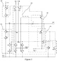
- a shift register unit provided in a first embodiment of the present disclosure has a structure as shown in Fig.1 . It can be seen from Fig.1 that the shift register unit comprises: an input module 101, a first output module 102, a pull-down driving module 103, a pull-down module 104 and a first output discharging module 105.
- the input module 101 is connected to an input signal terminal and a first clock signal input terminal in the shift register unit, and is configured to provide an input signal to a pull-up node in response to the input signal and a first clock signal.
- the pull-up node is a connection point between the input module and the first output module.
- the first output module 102 is connected to a second clock signal input terminal, and is configured to provide a second clock signal to a first output terminal in the shift register unit in response to a voltage signal at the pull-up node.
- the pull-down driving module 103 is connected to the first clock signal input terminal and the second clock signal input terminal, is configured to: provide the first clock signal to a first pull-down node in response to the first clock signal and provide the second clock signal to a second pull-down node in response to the second clock signal; provide a first low voltage signal to the first pull-down node and the second pull-down node in response to the voltage signal at the pull-up node; provide the first low voltage signal to the second pull-down node in response to a voltage signal at the first pull-down node; and provide the first low voltage signal to the first pull-down node in response to a voltage signal at the second pull-down node.
- the first pull-down node and the second pull-down node are both connection points between the pull-down driving module and the pull-down module.
- the pull-down module 104 is configured to provide the first low voltage signal to the pull-up node in response to the voltage signal at the first pull-down node and the voltage signal at the second pull-down node.
- the first output discharging unit 105 is configured to provide a second low voltage signal to the first output terminal of the shift register unit in response to the voltage signal at the first pull-down node and the voltage signal at the second pull-down node.
- the first low voltage signal is less than or equal to the second low voltage signal, and the first low voltage signal and the second low voltage signal are both negative voltages so as to pull down the potentials at the nodes and/or output terminals connected thereto.
- the shift register unit as shown in Fig.1 comprises: an input module 101, a first output module 102, a pull-down driving module 103, a pull-down module 104 and a first output discharging module 105.
- the input module 101 comprises: a first thin film transistor (TFT) T1 whose gate and source connected to the input signal terminal INPUT of the shift register unit and drain connected to a source of a second TFT T2; and the second TFT T2 whose gate connected to the first clock signal CK input terminal and drain connected to the pull-up node PU.
- TFT thin film transistor
- the input signal is provided to the pull-up node PU through the first TFT T1 and the second TFT T2, so as to make the potential at the pull-up node PU increased.
- the first output module 102 comprises: a third TFT T3 whose gate connected to the pull-up node PU, drain connected to the second clock signal CKB input terminal, and source connected to the first output terminal OT1; and a capacitor C connected between the pull-up node PU and the first output terminal OT1 and configured to keep the potential at the pull-up node PU, such that the third TFT T3 is kept turned on during a certain period.
- the pull-down driving module 103 comprises: a fourth TFT T4 whose gate and drain connected to the first clock signal CK input terminal, and source connected to the first pull-down node PD1; a fifth TFT T5 whose gate and source simultaneously connected to the second clock signal CKB input terminal, and drain connected to the second pull-down node PD2; a sixth TFT T6 whose gate connected to the pull-up node PU, drain connected to the first pull-down node PD1, and source connected to a drain of a seventh TFT T7; the seventh TFT T7 whose gate connected to the pull-up node PU and source connected to the first low voltage signal Vgl_1 input terminal; an eighth TFT T8 whose gate connected to the pull-up node PU, drain connected to the second pull-down node PD2, and source connected to a drain of a ninth TFT T9; the ninth TFT T9 whose gate connected to the pull-up node PU, and source connected to the first low voltage signal Vgl
- the pull-down driving module 103 charges the first pull-down node PD1 through the fourth TFT T4, charges the second pull-down node PD2 through the fifth TFT T5, discharges the first pull-down node PD1 through the sixth TFT T6, the seventh TFT T7 and the tenth TFT T10, and discharges the second pull-down node PD2 through the eighth TFT T8, the ninth TFT T9 and the eleventh TFT T11. Since the potential at the first pull-down node PD1 and the potential at the second pull-down node PD2 are AC signals during a non-outputting phase, the output errors caused by the drifts in the threshold voltages of the elements can be effectively suppressed, and thus the noise reduction effect can be increased.
- the first output discharging module 105 Since the voltage signal at the first pull-down node PD1 and the voltage signal at the second pull-down node PD2 are complementary, such that the first output discharging module 105 always discharges the first output terminal OT1 during the non-outputting phase, thus removing the output errors caused by the interval existed in the operation of pulling down the output terminal.
- the pull-down module 104 comprises: a twelfth TFT T12 whose gate connected to the first pull-down node PD1, source connected to the pull-up node PU, and drain connected to a drain of a thirteenth TFT T13; the thirteenth TFT T13 whose gate connected to the first pull-down node PD1 and drain connected to the first low voltage signal Vgl_1 input terminal; a fourteenth TFT T14 whose gate connected to the second pull-down node PD2, source connected to the pull-up node PU, and drain connected to a source of a fifteenth TFT T15; the fifteenth TFT T15 whose gate connected to the second pull-down node PD2, and drain connected to the first low voltage signal Vgl_1 input terminal.
- the pull-down module 104 discharges the pull-up node PU continuously in response to the voltage signal at the first pull-down node PD1 and the voltage signal at the second pull-down node PD2, so as to remove the noise caused by the AC signals.
- the first output discharging module 105 comprises: a sixteenth TFT T16 whose gate connected to the first pull-down node PD1, drain connected to the first output terminal OT1, and source connected to the second low voltage signal Vgl_2 input terminal; and a seventeenth TFT T17 whose gate connected to the second pull-down node PD2, drain connected to the first output terminal OT1, and source connected to the second low voltage signal Vgl_2 input terminal.
- the first output discharging module 105 discharges the first output terminal OT1 continuously during the non-outputting phase in response to the voltage signal at the first pull-down node PD1 and the voltage signal at the second pull-down node PD2, thus removing the noise caused by the AC signals.
- the pull-down driving module 104 is connected to the first clock signal CK input terminal and the second clock signal CKB input terminal, is configured to: provide the first clock signal CK to the first pull-down node PD1 in response to the first clock signal CK and provide the second clock signal CKB to the second pull-down node PD2 in response to the second clock signal CKB; provide the first low voltage signal Vgl_1 to the first pull-down node PD1 and the second pull-down node PD2 in response to the voltage signal at the pull-up node PU; provide the first low voltage signal Vgl_1 to the second pull-down node PD2 in response to the voltage signal at the first pull-down node PD1; and provide the first low voltage signal Vgl_1 to the first pull-down node PD1 in response to the voltage signal at the second pull-down node PD2.
- the voltage signal at the first pull-down node PD1 and the voltage signal at the second pull-down node PD2 are both AC signals so as to effectively suppress the output errors caused by the drifts in the threshold voltages of elements.
- the voltage signal at the first pull-down node PD1 and the voltage signal at the second pull-down node PD2 are complementary, such that the first output discharging module 105 always discharges the first output terminal OT1 during the non-outputting phase, thus removing the output errors caused by the interval existed in the operation of pulling down the first output terminal.
- a reset signal input terminal RESET connected simultaneously to the source of the sixth TFT T6 and the source of the eighth TFT T8.
- RESET reset signal input terminal
- the sources of the sixth TFT T6 and the eighth TFT T8 are also at the high level, such that the sixth TFT T6 and the eighth TFT T8 are turned off quickly, thus preventing dark current from flowing through the sixth TFT T6 to discharge the first pull-down node PD1 while preventing dark current from flowing through the eighth TFT T8 to discharge the second pull-down node PD2.
- the first low voltage signal Vgl_1 is less than the second low voltage signal Vgl_2, such that the sixteenth TFT T16 and the seventeenth TFT T17 are turned off more easily to effectively prevent dark currents from flowing through the sixteenth TFT T16 and the seventeenth TFT T17 to discharge the first output terminal OT1 during an output phase.
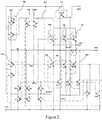
- Fig.2 shows a shift register unit provided in a second embodiment of the present disclosure.
- the shift register unit shown therein not only comprises an input module 101, a first output module 102, a pull-down driving module 103, a pull-down module 104 and a first output discharging module 105, but also comprises a second output module 106, a second output discharging module 107, a third output module 108, a third output discharging module 109 and a feedback module 110.
- the second output module 106 is connected to the second clock signal CKB input terminal, and is configured to provide the second clock signal CKB to a second output terminal OT2 in response to the voltage signal at the pull-up node PU so as to provide a reset signal for another shift register unit one-stage previous to the shift register unit.
- the second output module 106 comprises: an eighteenth TFT T18 whose gate connected to the pull-up node PU, drain connected to the second clock signal CKB input terminal, and source connected to the second output terminal OT2.
- the second output discharging module 107 is configured to provide the second low voltage signal Vgl_2 to the second output terminal OT2 in response to the voltage signal at the first pull-down node PD1 and the voltage signal at the second pull-down node PD2.
- the second output discharging module 107 comprises: a nineteenth TFT T19 whose gate connected to the first pull-down node PD1, drain connected to the second output terminal OT2, and source connected to the second low voltage signal Vgl_2 input terminal; and a twentieth TFT T20 whose gate connected to the second pull-down node PD2, drain connected to the second output terminal OT2, and source connected to the second low voltage signal Vgl_2 input terminal.
- the second output discharging module 107 discharges the second output terminal OT2 continuously during the non-outputting phase in response to the voltage signal at the first pull-down node PD1 and the voltage signal at the second pull-down node PD2, thus removing the noise caused by the AC signals.
- the third output module 108 is connected to the second clock signal CKB input terminal, and is configured to provide the second clock signal CKB to a third output terminal OT3 in response to the voltage signal at the pull-up node PU so as to provide a start signal for another shift register unit one-stage next to the shift register unit.
- the third output module 108 comprises: a twenty-first TFT T21 whose gate connected to the pull-up node PU, drain connected to the second clock signal CKB input terminal, and source connected to the third output terminal OT3.
- the third output discharging module 109 is configured to provide the first low voltage signal Vgl_1 to the third output terminal OT3 in response to the voltage signal at the first pull-down node PD1 and the voltage signal at the second pull-down node PD2, so as to provide a start signal for another shift register unit one-stage next to the shift register unit.
- the third output discharging module 109 comprises: a twenty-second TFT T22 whose gate connected to the first pull-down node PD1, drain connected to the third output terminal OT3, and source connected to the first low voltage signal Vgl_1 input terminal; and a twenty-third TFT T23 whose gate connected to the second pull-down node PD2, drain connected to the third output terminal OT3, and source connected to the first low voltage signal Vgl_1 input terminal.
- the third output discharging module 109 discharges the third output terminal OT3 continuously during the non-outputting phase in response to the voltage signal at the first pull-down node PD1 and the voltage signal at the second pull-down node PD2, thus removing the noise caused by the AC signals.
- the feedback module 110 is configured to provide the voltage signal at the second output terminal OT2 to the input module 101 and the pull-down module 104 in response to the voltage signal at the third output terminal OT3.
- the feedback module 110 comprises: a twenty-fourth TFT T24 whose gate connected to the third output terminal OT3, drain connected to the drain of the first TFT T1, the drain of the twelfth TFT T12 and the drain of the fourteenth TFT T14, and source connected to the second output terminal OT2.
- the source of the second TFT T2 When the output at the second output terminal OT2 is the high level, the source of the second TFT T2, the source of the thirteenth TFT T13 and the source of the fifteenth TFT T15 are all at the high level, such that the second TFT T2, the thirteenth TFT T13 and the fifteenth TFT T15 are all turned off, and at this time the first TFT T1, the twelfth TFT T12 and the fourteenth TFT T14 are also completely turned off, thus preventing dark currents from being generated in the second TFT T2, the twelfth TFT T12 and the fourteenth TFT T14 to discharge pull-up node PU.
- the capacitor C can be set between the pull-up node PU and the first output terminal OT1, or can be set between the pull-up node PU and the second output terminal OT2, and can also be set between the pull-up node PU and the third output terminal OT3. In these three connection manners, the function of the capacitor is the same to keep the potential at the pull-up node PU.
- one electrode with an arrow is a source of the TFT, and the direction of the arrow is a current direction in the TFT.
- an error in the output of a certain stage of shift register unit has no effect on the operation states of another shift register units one-stage pervious to the shift register unit and another shift register one-stage next to the shift register unit, since the reset signal and the start signal are output though separate circuits.
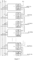
- the above described shift register units are connected in cascade to form a gate driver circuit on array substrate.
- the gate driver circuit provided in the embodiments of the present disclosure comprises respective stages of shift register units connected in cascade, wherein the input signal terminal of a first stage of shift register unit is connected to a start signal terminal of the gate driver circuit, the reset signal terminal of the first stage of shift register unit is connected to any one of the output terminals of a second stage of shift register unit, the input signal terminal of a last stage of shift register unit is connected to any one of the output terminals of its previous stage of shift register unit, and the reset signal terminal of the last stage of shift register unit is connected to the start signal terminal.
- each of the shift register units connected in cascade as above is the shift register unit as shown in Fig.1 or the shift register unit as shown in Fig.2 .
- the gate driver circuit on array substrate comprises N stages of shift register units, wherein N is the number of gate lines, the start signal STV is input to the first stage of shift register unit as the input signal, and gate driving signals are output to respective gate lines sequentially, the input signal of a n th stage of shift register unit is supplied by the output signal of a (n-1) th stage of shift register unit, and the reset signal of the n th stage of shift register unit is supplied by the output signal of a (n+1) th stage of shift register unit, where n ⁇ N.
- Fig.3 shows a gate driver circuit on array substrate formed by the shift register units as shown in Fig.1 connected in cascade as provided in a third embodiment of the present disclosure.
- Fig.4 is a timing diagram of signals at respective signal terminals in the shift register unit. Below, the operating method of the n th stage of shift register unit in the gate driver circuit on array substrate as provided in the embodiment of the present disclosure will be described with reference to Fig.4 , where n ⁇ N and N is the number of stages of shift register units in the gate driver circuit on array substrate.
- the gate driver circuit When the gate driver circuit performs the scanning operation, all of TFTs in the gate driver circuit are turned on at a high level, and are turned off at a low level.
- the first clock signal CK and the second clock signal CKB have phases opposites to each other.
- the first clock signal CK is at the low level and the second clock signal CKB is at the high level
- the output signal OUTPUT(n-1) of the (n-1) th stage of shift register unit being the input signal of the n th stage of shift register unit is at the low level
- the output signal OUTPUT(n+1) of the (n+1) th stage of shift register unit being the reset signal of the n th stage of shift register unit is at the low level
- the first pull-down node PD1 is at the low level
- the second pull-down node PD2 is at the high level.
- the tenth TFT T10, the fourteenth TFT T14, the fifteenth TFT T15 and the seventeenth TFT T17 are turned on in response to the high level voltage signal at the second pull-down node PD2, the fourteenth TFT T14 and the fifteenth TFT T15 provide the first low voltage signal Vg1_1 to the pull-up node PU, the tenth TFT T10 provide the first low voltage signal Vg1_1 to the first pull-down node PD1, and the seventeenth TFT T17 provides the second low voltage signal Vg1_2 to the first output terminal OT1.
- the output signal OUTPUT(n) at the first output terminal OT1 is at the low level at this time.
- the first clock signal CK is at the high level
- the second clock signal CKB is at the low level
- OUTPUT(n-1) is at the high level
- OUTPUT(n+1) is at the low level.
- the first TFT T1 is turned on since the input signal OUTPUT(n-1) is at the high level
- the second TFT T2 is turned on since the first clock signal CK is at the high level
- the input signal charges the capacitor C through the first TFT T1 and the second TFT T2, and the pull-up node PU is at the high level.
- the third TFT T3 is turned on in response to the voltage signal at the pull-up node PU, but the output signal OUTPUT(n) at the first output terminal OT1 is at the low level since the second clock signal CKB is at the low level.
- the sixth TFT T6, the seventh TFT T7, the eighth TFT T8 and the ninth TFT T9 are turned on in response to the voltage signal at the pull-up node PU; the first pull-down node PD1 is discharged continuously through the sixth TFT T6 and the seventh TFT T7 and thus keeps at the low level; the second pull-down node PD2 is discharged through the eighth TFT T8 and the ninth TFT T9, and the potential at the second pull-down node PD2 is decreased rapidly.
- the first clock signal CK is at the low level
- the second clock signal CKB is at the high level
- OUTPUT(n-1) is at the low level
- OUTPUT(n+1) is at the low level.
- the first TFT T1 is turned off since the input signal OUTPUT(n-1) is at the low level
- the second TFT T2 is turned off since the first clock signal CK is at the low level, but the pull-up node PU is kept at the high level due to the capacitor C.
- the second clock signal CKB is at the high level, and the potential at the pull-up node PU is increased continuously due to the bootstrapping function of the capacitor C, such that the third TFT T3 is kept turned on.
- the sixth TFT T6, the seventh TFT T7, the eighth TFT T8 and the ninth TFT T9 are kept turned on in response to the voltage signal at the pull-up node PU, and the first pull-down node PD1 and the second pull-down node PD2 are at the low level.
- the sixteenth TFT T16 is turned off in response to the low level voltage signal at the first pull-down node PD1
- the seventeenth TFT T17 is turned off in response to the high level voltage signal at the second pull-down node PD2.
- the output signal OUTPUT(n) at the first output terminal OT1 is at the high level.
- the first clock signal CK is at the high level
- the second clock signal CKB is at the low level
- OUTPUT(n-1) is at the low level
- OUTPUT(n+1) is at the high level.
- the sixth TFT T6, the seventh TFT T7, the eighth TFT T8 and the ninth TFT T9 are completely turned off since OUTPUT(n+1) is at the high level.
- the fourth TFT T4 is turned on since the first clock signal CK is at the high level to provide the first clock signal CK to the first pull-down node PD1, the first pull-down node PD1 is increased to the high level.
- the eleventh TFT T11, the twelfth TFT T12, the thirteenth TFT T13 and the sixteenth TFT T16 are turned on in response to the high level voltage signal at the first pull-down node PD1, the twelfth TFT T12 and the thirteenth TFT T13 discharge the pull-up node PU, the pull-up node PU is decreased rapidly to the low level; the eleventh TFT T11 provides the first low voltage signal Vg1_1 to the second pull-down node PD2, the second pull-down node PD2 is kept at the low level; and the sixteenth TFT T16 provides the second low voltage signal Vgl_2 to the first output terminal OT1.
- the output signal OUTPUT(n) at the first output terminal OT1 is at the low level at this time.
- the first clock signal CK is at the low level
- the second clock signal CKB is at the high level
- OUTPUT(n-1) is at the low level
- OUTPUT(n+1) is at the low level.
- the fifth TFT T5 is turned on since the second clock signal CKB is at the high level, the eighth TFT T8 and the ninth TFT T9 are kept turned off in response to the voltage signal at the pull-up node PU, the second pull-down node PD2 is increased to the high level, the tenth TFT T10, the fourteenth TFT T14, the fifteenth TFT T15 and the seventeenth TFT T17 are turned on in response to the high level voltage signal at the second pull-down node PD2, the tenth TFT T10 provides the first low voltage signal Vgl_1 to the first pull-down node PD1, and the first pull-down node PD1 is kept at the low level; the fourteenth TFT T14 and the fifteenth TFT T15 discharges the pull-up node PU continuously, the pull-up node PU is kept at the low level and thus the third TFT T3 is turned off; meanwhile the seventeenth TFT T17 provides the second low voltage signal Vgl_2 to the first output terminal OT
- the output signal OUTPUT(n) at the first output terminal OT1 is at the low level.
- Fig.5 shows a gate driver circuit on array substrate constituted by the shift register unit as shown in Fig.1 provided in a fourth embodiment of the present disclosure.
- the first output terminal OT1(n) of the n th stage of shift register unit provides a signal for the present row
- the second output terminal OT2(n) of the n th stage of shift register unit provides a reset signal to the (n-1) th stage of shift register unit
- the third output terminal OT3(n) of the n th stage of shift register unit provides a start signal to the (n+1) th stage of shift register unit.
- the first output terminal OT1(n), the second output terminal OT2(n) and the third output terminal OT3(n) have the same output signal, which is OUTPUT(n).
- n ⁇ N and N is the number of stages of shift register units in the gate driver circuit on array substrate.
- the first clock signal CK is at the low level and the second clock signal CKB is at the high level
- the output signal OUTPUT(n-1) of the (n-1) th stage of shift register unit being the input signal of the n th stage of shift register unit is at the low level
- the output signal OUTPUT(n+1) of the (n+1) th stage of shift register unit being the reset signal of the n th stage of shift register unit is at the low level
- the first pull-down node PD1 is at the low level
- the second pull-down node PD2 is at the high level.
- the tenth TFT T10, the fourteenth TFT T14, the fifteenth TFT T15 and the seventeenth TFT T17 are turned on in response to the high level voltage signal at the second pull-down node PD2.
- the tenth TFT T10 provide the first low voltage signal Vg1_1 to the first pull-down node PD1;
- the fourteenth TFT T14 and the fifteenth TFT T15 provide the first low voltage signal Vg1_1 to the pull-up node PU,
- the third TFT T3, the eighteenth TFT T18 and the twenty-first TFT T21 are turned off in response to the voltage signal at the pull-up node PU;
- the seventeenth TFT T17 provides the second low voltage signal Vgl_2 to the first output terminal OT1(n)
- the twentieth TFT T20 provides the second low voltage signal Vg1_2 to the second output terminal OT2(n)
- the twenty-third TFT T23 provides the first low voltage signal Vgl_1 to the
- the output signal OUTPUT(n) at the first output terminal OT1(n), the output signal OUTPUT(n) at the second output terminal OT2(n) at the output signal OUTPUT(n) at the third output terminal OT3(n) are all at the low level.
- the first clock signal CK is at the high level
- the second clock signal CKB is at the low level
- OUTPUT(n-1) is at the high level
- OUTPUT(n+1) is at the low level.
- the first TFT T1 is turned on since the input signal OUTPUT(n-1) is at the high level
- the second TFT T2 is turned on since the first clock signal CK is at the high level
- the input signal charges the capacitor C through the first TFT T1 and the second TFT T2, such that the pull-up node PU is at the high level.
- the third TFT T3, the eighteenth TFT T18 and the twenty-first TFT T21 are turned on in response to the voltage signal at the pull-up node PU.
- the output signal OUTPUT(n) at the first output terminal OT1(n), the output signal OUTPUT(n) at the second output terminal OT2(n) and the output signal OUTPUT(n) at the third output terminal OT3(n) are all at the low level since the second clock signal CKB is at the low level.
- the sixth TFT T6, the seventh TFT T7, the eighth TFT T8 and the ninth TFT T9 are turned on in response to the voltage signal at the pull-up node PU; the first pull-down node PD1 is discharged continuously through the sixth TFT T6 and the seventh TFT T7 and thus keeps at the low level; the second pull-down node PD2 is discharged continuously through the eighth TFT T8 and the ninth TFT T9, such that the potential at the second pull-down node PD2is decreased rapidly.
- the first clock signal CK is at the low level
- the second clock signal CKB is at the high level
- OUTPUT(n-1) is at the low level
- OUTPUT(n+1) is at the low level.
- the first TFT T1 is turned off since the input signal OUTPUT(n-1) is at the low level
- the second TFT T2 is turned off since the first clock signal CK is at the low level, but the pull-up node PU is still kept at the high level due to the capacitor C.
- the second clock signal CKB is at the high level
- the potential at the pull-up node PU is increased continuously due to the bootstrapping function of the capacitor C
- the third TFT T3, the eighteenth TFT T18 and the twenty-first TFT T21 are kept turned on.
- the sixth TFT T6, the seventh TFT T7, the eighth TFT T8 and the ninth TFT T9 are kept turned on in response to the voltage signal at the pull-up node PU, and the first pull-down node PD1 and the second pull-down node PD2 are at the low level.
- the sixteenth TFT T16, the nineteenth TFT T19 and the twenty-second TFT T22 are turned off in response to the voltage signal at the first pull-down node PD1
- the seventeenth TFT T17, twentieth TFT T20 and the twenty-third TFT T23 are turned off in response to the voltage signal at the second pull-down node PD2.
- the output signal OUTPUT(n) at the first output terminal OT1(n), the output signal OUTPUT(n) at the second output terminal OT2(n) and the output signal OUTPUT(n) at the third output terminal OT3(n) are at the high level.
- the twenty-fourth TFT T24 is turned on in response to the voltage signal at the second output terminal OT2(n), such that the potential at the source of the second TFT T2, the potential at the drain of the twelfth TFT T12 and the potential at the drain of the fourteenth TFT T14 are increased, and thus the second TFT T2, the twelfth TFT T12 and the fourteenth TFT T14 are completely turned off so as to prevent the dark currents therein from discharging the pull-up node PU.
- the first clock signal CK is at the high level
- the second clock signal CKB is at the low level
- OUTPUT(n-1) is at the low level
- OUTPUT(n+1) is at the high level.
- the sixth TFT T6, the seventh TFT T7, the eighth TFT T8 and the ninth TFT T9 are turned off since OUTPUT(n+1) is at the high level.
- the fourth TFT T4 is turned on since the first clock signal CK is at the high level to provide the first clock signal CK to the first pull-down node PD1, the first pull-down node PD1 is increased to the high level.
- the eleventh TFT T11, the twelfth TFT T12, the thirteenth TFT T13, the sixteenth TFT T16, the nineteenth TFT T19 and the twenty-second TFT T22 are turned on in response to the voltage signal at the first pull-down node PD1, the twelfth TFT T12 and the thirteenth TFT T13 discharge the pull-up node PU, and the pull-up node PU is decreased rapidly to the low level; the eleventh TFT T11 provides the first low voltage signal Vgl_1 to the second pull-down node PD2, and the second pull-down node PD2 is kept at the low level; and the sixteenth TFT T16 provides the second low voltage signal Vgl_2 to the first output terminal OT1(n), the nineteenth TFT T19 provides the second low voltage signal Vg1_2 to the second output terminal OT2(n), and the twenty-second TFT T22 provides the first low voltage signal Vgl_1 to the third output terminal OT3(n).
- the output signal OUTPUT(n) at the first output terminal OT1(n), the output signal OUTPUT(n) at the second output terminal OT2(n) and the output signal OUTPUT(n) at the third output terminal OT3(n) are at the low level.
- the first clock signal CK is at the low level
- the second clock signal CKB is at the high level
- OUTPUT(n-1) is at the low level
- OUTPUT(n+1) is at the high level.
- the fifth TFT T5 is turned on since the second clock signal CKB is at the high level, the eighth TFT T8 and the ninth TFT T9 are kept turned off in response to the voltage signal at the pull-up node PU, and the second pull-down node PD2 is increased to the high level.
- the tenth TFT T10, the fourteenth TFT T14, the fifteenth TFT T15, the seventeenth TFT T17, the twentieth TFT T20 and the twenty-third TFT T23 are turned on in response to the voltage signal at the second pull-down node PD2, the tenth TFT T10 provides the first low voltage signal Vgl_1 to the first pull-down node PD1, and the first pull-down node PD1 is kept at the low level; the fourteenth TFT T14 and the fifteenth TFT T15 discharges the pull-up node PU continuously, and the pull-up node PU is kept at the low level and thus the third TFT T3, the eighteenth TFT T18 and the twenty-first TFT T21 are turned off; the seventeenth TFT T17 provides the second low voltage signal Vg1_2 to first output terminal OT1(n), the twentieth TFT T20 provides the second low voltage signal Vg1_2 to the second output terminal OT2(n), and the twenty-third TFT T23 provides
- the output signal OUTPUT(n) at the first output terminal OT1(n), the output signal OUTPUT(n) at the second output terminal OT2(n) and the output signal OUTPUT(n) at the third output terminal OT3(n) are all at the low level.
- the pull-down driving module is connected to the first clock signal input terminal and the second clock signal input terminal, is configured to: provide the first clock signal to the first pull-down node in response to the first clock signal and provide the second clock signal to the second pull-down node in response to the second clock signal; provide the first low voltage signal to the first pull-down node and the second pull-down node in response to the voltage signal at the pull-up node; provide the first low voltage signal to the second pull-down node in response to the voltage signal at the first pull-down node; and provide the first low voltage signal to the first pull-down node in response to the voltage signal at the second pull-down node.
- the first pull-down node and the second pull-down node are connection points between the pull-down driving module and the pull-down module.
- the voltage signal at the first pull-down node and the voltage signal at the second pull-down node are AC signals to effectively suppress the output errors caused by the drifts in the threshold voltages of elements.
- the voltage signal at the first pull-down node and the voltage signal at the second pull-down node are complementary, such that the first output discharging module always discharges the first output terminal during the non-outputting phase, thus removing the output errors caused by the interval existed in the operation of pulling down the first output terminal.
Description
- The present disclosure relates to the technical field of liquid crystal display, and particularly to a shift register unit and a gate driver circuit.
- Drivers in a thin film transistor liquid crystal display (TFT-LCD) mainly comprise a gate driver circuit and a data driver circuit. The gate driver circuit converts an inputted clock signal through shift register units and then supplies the converted clock signal on gate lines of a liquid crystal display (LCD) panel. The gate driver circuit can be formed on the LCD panel together with TFTs in a same process. The gate driver circuit comprises a plurality of stages of shift register units, and each stage of shift register unit is connected to a corresponding gate line and outputs a gate driving signal. The respective stages of shift register units are connected each other, a start signal is input to the first stage of the respective stages, and gate driving signals are output to the gate lines sequentially. An input terminal of a present stage of shift register unit is connected to an output terminal of a previous stage of shift register unit, and an output terminal of a next stage of shift register unit is connected to a control terminal of the present stage of shift register unit.
- The above structured gate driver circuit is set on the LCD panel. At present, in a gate driver circuit design, a pull-down node is generally arranged to pull down the potential at an output terminal of a shift register unit not corresponding to a row to which a gate driving signal is output. However, if the pull-down node is in a direct current (DC) high level operation state for a long time, it would cause drifts in threshold voltages of relevant thin film transistors, which has a disadvantageous effect on noise reduction. On the other hand, if the voltage signal at the pull-down node is a alternate current (AC) signal, effect caused by the drifts in the threshold voltages may be reduced, however output errors may occur and in turn reading and writing errors may be generated since there is a interval in the operation of pulling down with the alternate current signal. From
CN 102867543 A it is known a shifting register, a grid driver and a display device.CN 102682699 A discloses a grid electrode driving circuit and display. - In order to solve the technical problem in the prior art, in embodiments of the present disclosure, there are provided a shift register unit and a gate driver circuit, which are configured to suppress output errors caused by the drifts in the threshold voltages and the interval existed in the operation of pulling down the output terminal, and thus to enhance the stability of the shift register unit.
- The shift register unit according to
claim 1 comprises: an input module comprising a first thin film transistor TFT and a second TFT, wherein a gate and a source of the first TFT are both connected with an input signal terminal of the shift register unit, a drain of the first TFT is connected with a source of the second TFT, a gate and a drain of the second TFT are connected respectively to a first clock signal input terminal of the shift register unit and a pull-up node in the shift register unit;
a first output module comprising a third TFT and a capacitor, wherein a gate, drain and source of the third TFT are connected respectively with the pull-up node, a second clock signal input terminal and a first output terminal of the shift register unit, and the capacitor is connected between the pull-up node and the first output terminal;
a pull-down driving module comprising a fourth TFT, a fifth TFT, a sixth TFT, a seventh TFT, an eighth TFT, a ninth TFT, a tenth TFT and an eleventh TFT, wherein a gate and a drain of the fourth TFT are both connected to the first clock signal input terminal, a gate and a drain of the fifth TFT are both connected with the second clock signal input terminal, a source of the fourth TFT and a source of the fifth TFT are connected respectively with a first pull-down node and a second pull-down node in the shift register unit, a gate of the sixth TFT and a gate of the seventh TFT are both connected with the pull-up node, a drain and source of the sixth TFT are connected respectively with the first pull-down node and a reset signal terminal of the shift register unit, a drain and source of the seventh TFT are connected respectively with the reset signal terminal and a first low voltage signal input terminal of the shift register unit, a gate of the eighth TFT and a gate of the ninth TFT are both connected with the pull-up node, a drain and source of the eighth TFT are connected respectively with the second pull-down node and the reset signal terminal, a drain and source of the ninth TFT are connected respectively with the reset signal terminal and the first low voltage signal input terminal, a gate and source of the eleventh TFT are connected respectively with the first pull-down node and the second pull-down node, a gate and drain of the tenth TFT are connected respectively with the second pull-down node and the first pull-down node, and a drain of the eleventh TFT and a source of the tenth TFT are both connected with the first low voltage signal input terminal;
a pull-down module comprising a twelfth TFT, a thirteenth TFT, a fourteenth TFT and a fifteenth TFT, wherein a gate of the twelfth TFT and a gate of the thirteenth TFT are both connected with the first pull-down node, a source and drain of the twelfth TFT are connected respectively with the pull-up node and a source of the thirteenth TFT, a drain of the thirteenth TFT is connected to the first low voltage signal input terminal, a gate of the fourteenth TFT and a gate of the fifteenth TFT are both connected with the second pull-down node, a source and drain of the fourteenth TFT are connected respectively with the pull-up node and a source of the fifteenth TFT, a drain of the fifteenth TFT is connected to the first low voltage signal input terminal;
a first output discharging module comprising an sixteenth TFT and a seventeenth TFT, wherein a gate of the sixteenth TFT and a gate of the seventeenth TFT are connected respectively with the first pull-down node and the second pull-down node, a drain of the sixteenth TFT and a drain of the seventeenth TFT are both connected with the first output terminal, and a source of the sixteenth TFT and a source of the seventeenth TFT are both connected with a second low voltage signal input terminal of the shift register unit. - In the shift register unit, the pull-down driving module is connected to the first clock signal input terminal and the second clock signal input terminal, and is configured to provide the first clock signal to the first pull-down node in response to the first clock signal, provide the second clock signal to the second pull-down node in response to the second clock signal; provide the first low voltage signal to the first pull-down node and the second pull-down node in response to the voltage signal at the pull-up node; provide the first low voltage signal to the second pull-down node in response to the voltage signal at the first pull-down node; and provide the first low voltage signal to the first pull-down node in response to the voltage signal at the second pull-down node. Herein, the first pull-down node and the second pull-down node are both connection points of the pull-down driving module and the pull-down module. During a non-outputting phase, the voltage signal at the first pull-down node and the voltage signal at the second node are AC signals to effectively suppress the output errors caused by the drifts in the threshold voltages of elements, and thus the noise reduction effect is increased. Meanwhile, the voltage signal at the first pull-down node and the voltage signal at the second node are complementary, such that the first output discharging module always discharges the first output terminal during the non-outputting phase, thus removing the output errors caused by the time interval in which the first output terminal is not pulled down during the period in which the first output terminal should be pulled down.
- The input signal is provided to the pull-up node through the first TFT and the second TFT, so as to make the potential at the pull-up node increased.
- When the pull-up node is at a high level, the third TFT is turned on, and then the second clock signal can be provided to the output terminal through the third TFT; the capacitor is configured to keep the potential at the pull-up node, such that the third TFT is kept turned on during a certain period.
- The pull-down driving module charges the first pull-down node through the fourth TFT, charges the second pull-down node through the fifth TFT, discharges the first pull-down node through the sixth TFT, the seventh TFT and the tenth TFT, and discharges the second pull-down node through the eighth TFT, the ninth TFT and the eleventh TFT. Since the potential at the first pull-down node and the potential at the second pull-down node are both AC signals during the non-outputting phase, the output errors caused by the drifts in the threshold voltages of the elements can be effectively suppressed, and thus the noise reduction effect can be increased. Since the voltage signal at the first pull-down node and the voltage signal at the second pull-down node are complementary, such that the first output discharging module always discharges the first output terminal during the non-outputting phase, thus removing the output errors caused by the interval existed in the operation of pulling down the first output terminal.
- The pull-down module discharges the pull-up node continuously in response to the voltage signal at the first pull-down node and the voltage signal at the second pull-down node, so as to remove the noise caused by the AC signals.
- The first output discharging module discharges the first output terminal continuously during the non-outputting phase in response to the voltage signal at the first pull-down node and the voltage signal at the second pull-down node, thus removing the noise caused by the AC signals.
- Optionally, the shift register unit further comprises: a second output module connected to the second clock signal input terminal and configured to provide the second clock signal to a second output terminal of the shift register unit in response to the voltage signal at the pull-up node to provide a reset signal for another shift register unit one-stage previous to the shift register unit.
- Further, the second output module comprises: an eighteenth TFT whose gate connected to the pull-up node, drain connected to the second clock signal input terminal, and source connected to the second output terminal.
- Optionally, the shift register unit further comprises: a second output discharging module configured to provide the second low voltage signal to the second output terminal in response to the voltage signal at the first pull-down node and the voltage signal at the second pull-down node.
- The second output discharging module comprises: a nineteenth TFT whose gate connected to the first pull-down node, drain connected to the second output terminal, and source connected to the second low voltage signal input terminal; and a twentieth TFT whose gate connected to the second pull-down node, drain connected to the second output terminal, and source connected to the second low voltage signal input terminal.
- The second output discharging module discharges the second output terminal continuously during the non-outputting phase in response to the voltage signal at the first pull-down node and the voltage signal at the second pull-down node, thus removing the noise caused by the AC signals.
- Optionally, the shift register unit further comprises a third output module connected to the second clock signal input terminal and configured to provide the second clock signal to a third output terminal in response to the voltage signal at the pull-up node to provide a start signal for another shift register unit one-stage next to the shift register unit.
- Further, the third output module comprises: a twenty-first TFT whose gate connected to the pull-up node, drain connected to the second clock signal input terminal, and source connected to the third output terminal.
- Optionally, the shift register unit further comprises a third output discharging module configured to provide the first low voltage signal to the third output terminal in response to the voltage signal at the first pull-down node and the voltage signal at the second pull-down node.
- The third output discharging module comprises: a twenty-second TFT whose gate connected to the first pull-down node, drain connected to the third output terminal, and source connected to the first low voltage signal input terminal; and a twenty-third TFT whose gate connected to the second pull-down node, drain connected to the third output terminal, and source connected to the first low voltage signal input terminal.
- The third output discharging module discharges the third output terminal continuously during the non-outputting phase in response to the voltage signal at the first pull-down node and the voltage signal at the second pull-down node, thus removing the noise caused by the AC signals.
- Optionally, the shift register unit further comprises a feedback module configured to provide the voltage signal at the second output terminal to the input module and the pull-down module in response to the voltage signal at the third output terminal.
- Furthermore, the feedback module comprises: a twenty-fourth TFT whose gate connected to the third output terminal, drain connected to the source of the second TFT, the drain of the twelfth TFT and the drain of the fourteenth TFT, and source connected to the second output terminal.
- When the voltage signal in the feedback circuit is at a high level, the source of the second TFT, the source of the thirteenth TFT and the source of the fifteenth TFT are all at the high level, such that the second TFT T2, the thirteenth TFT T13 and the fifteenth TFT T15 are turned off, and meanwhile the first TFT, the twelfth TFT and the fourteenth TFT are completely turned off. Therefore, it can be effectively avoided that dark currents in the first TFT and the second TFT make the pull-up node discharged, dark currents in the twelfth TFT and the thirteenth TFT make the pull-up node discharged, and dark currents in the fourteenth TFT and the fifteenth TFT make the pull-up node discharged.
- Optionally, the first low voltage signal is less than the second low voltage signal, and the potentials at the first pull-down node and the second pull-down node are less than the potential of the second low voltage when the potentials at the first pull-down node and the second pull-down node are both a low level, such that the transistors whose gates connected to the first pull-down node or the second pull-down node and sources connected to the second low voltage signal input terminal are more easily turned off, and the dark currents are effectively prevented from being generated.
- The gate driver circuit provided by claim 12 comprises respective stages of shift register units according to the invention, wherein respective stages of shift register units being connected in cascade, the input signal terminal of a first stage of shift register unit is connected to a start signal terminal of the gate driver circuit, the reset signal terminal of the first stage of shift register unit is connected to any one of the output terminals of a second stage of shift register unit, the input signal terminal of a last stage of shift register unit is connected to any one of the output terminals of its previous stage of shift register unit, and the reset signal terminal of the last stage of shift register unit is connected to the start signal terminal. Except for the first stage and the last stage of shift register units, the input signal terminal of each of other stages of shift register units is connected to any one of the output terminals of its previous stage of shift register unit, and the reset signal terminal of each of other stages of shift register units is connected to any one of the output terminals of its next stage of shift register unit. All the shift register units connected in cascade are the above mentioned shift register unit.
-
-
Fig.1 is a schematic diagram of a structure of a shift register unit provided in a first embodiment of the present disclosure; -
Fig.2 is a schematic diagram of a structure of another shift register unit provided in a second embodiment of the present disclosure; -
Fig.3 is a schematic diagram of a structure of a gate driver circuit constituted by the shift register unit as shown inFig.1 provided in a third embodiment of the present disclosure; -
Fig.4 is a timing diagram of signals at respective signal terminals in the shift register unit provided in the first embodiment of the present disclosure; and -
Fig.5 is a schematic structure diagram of a structure of a gate driver circuit constituted by the shift register unit as shown inFig.1 provided in a fourth embodiment of the present disclosure. - In the embodiments of the present disclosure, there are provided a shift register unit and a gate driver circuit, which are configured to suppress output errors caused by the drifts in the threshold voltages and the time interval in which the output terminal is not pulled down during the period in which the output terminal should be pulled down, and thus to increase stability of the shift register unit.
- Below, descriptions will be given to the embodiments of the present disclosure with reference to the accompanying drawings.
- A shift register unit provided in a first embodiment of the present disclosure has a structure as shown in
Fig.1 . It can be seen fromFig.1 that the shift register unit comprises: aninput module 101, afirst output module 102, a pull-down driving module 103, a pull-down module 104 and a firstoutput discharging module 105. - The
input module 101 is connected to an input signal terminal and a first clock signal input terminal in the shift register unit, and is configured to provide an input signal to a pull-up node in response to the input signal and a first clock signal. The pull-up node is a connection point between the input module and the first output module. - The
first output module 102 is connected to a second clock signal input terminal, and is configured to provide a second clock signal to a first output terminal in the shift register unit in response to a voltage signal at the pull-up node. - The pull-down
driving module 103 is connected to the first clock signal input terminal and the second clock signal input terminal, is configured to: provide the first clock signal to a first pull-down node in response to the first clock signal and provide the second clock signal to a second pull-down node in response to the second clock signal; provide a first low voltage signal to the first pull-down node and the second pull-down node in response to the voltage signal at the pull-up node; provide the first low voltage signal to the second pull-down node in response to a voltage signal at the first pull-down node; and provide the first low voltage signal to the first pull-down node in response to a voltage signal at the second pull-down node. The first pull-down node and the second pull-down node are both connection points between the pull-down driving module and the pull-down module. - The pull-
down module 104 is configured to provide the first low voltage signal to the pull-up node in response to the voltage signal at the first pull-down node and the voltage signal at the second pull-down node. - The first
output discharging unit 105 is configured to provide a second low voltage signal to the first output terminal of the shift register unit in response to the voltage signal at the first pull-down node and the voltage signal at the second pull-down node. - In this embodiment, the first low voltage signal is less than or equal to the second low voltage signal, and the first low voltage signal and the second low voltage signal are both negative voltages so as to pull down the potentials at the nodes and/or output terminals connected thereto.
- The operating principle of the present disclosure will be described in detail below with refer to specific embodiments. It should be noted that the embodiments are just for better explanations of the present disclosure and make no limitation on the present disclosure.
- The shift register unit as shown in
Fig.1 comprises: aninput module 101, afirst output module 102, a pull-downdriving module 103, a pull-down module 104 and a firstoutput discharging module 105. - Specifically, the
input module 101 comprises: a first thin film transistor (TFT) T1 whose gate and source connected to the input signal terminal INPUT of the shift register unit and drain connected to a source of a second TFT T2; and the second TFT T2 whose gate connected to the first clock signal CK input terminal and drain connected to the pull-up node PU. - The input signal is provided to the pull-up node PU through the first TFT T1 and the second TFT T2, so as to make the potential at the pull-up node PU increased.
- The
first output module 102 comprises: a third TFT T3 whose gate connected to the pull-up node PU, drain connected to the second clock signal CKB input terminal, and source connected to the first output terminal OT1; and a capacitor C connected between the pull-up node PU and the first output terminal OT1 and configured to keep the potential at the pull-up node PU, such that the third TFT T3 is kept turned on during a certain period.. - The pull-down driving module 103 comprises: a fourth TFT T4 whose gate and drain connected to the first clock signal CK input terminal, and source connected to the first pull-down node PD1; a fifth TFT T5 whose gate and source simultaneously connected to the second clock signal CKB input terminal, and drain connected to the second pull-down node PD2; a sixth TFT T6 whose gate connected to the pull-up node PU, drain connected to the first pull-down node PD1, and source connected to a drain of a seventh TFT T7; the seventh TFT T7 whose gate connected to the pull-up node PU and source connected to the first low voltage signal Vgl_1 input terminal; an eighth TFT T8 whose gate connected to the pull-up node PU, drain connected to the second pull-down node PD2, and source connected to a drain of a ninth TFT T9; the ninth TFT T9 whose gate connected to the pull-up node PU, and source connected to the first low voltage signal Vgl_1 input terminal; a tenth TFT T10 whose gate connected to the second pull-down node PD2, drain connected to the first pull-down node PD1, and source connected to the first low voltage signal Vgl_1 input terminal; and an eleventh TFT T11 whose gate connected to the first pull-down node PD1, source connected to the second pull-down node PD2, and drain connected to the first low voltage signal Vgl_1 input terminal.
- The pull-down
driving module 103 charges the first pull-down node PD1 through the fourth TFT T4, charges the second pull-down node PD2 through the fifth TFT T5, discharges the first pull-down node PD1 through the sixth TFT T6, the seventh TFT T7 and the tenth TFT T10, and discharges the second pull-down node PD2 through the eighth TFT T8, the ninth TFT T9 and the eleventh TFT T11. Since the potential at the first pull-down node PD1 and the potential at the second pull-down node PD2 are AC signals during a non-outputting phase, the output errors caused by the drifts in the threshold voltages of the elements can be effectively suppressed, and thus the noise reduction effect can be increased. Since the voltage signal at the first pull-down node PD1 and the voltage signal at the second pull-down node PD2 are complementary, such that the firstoutput discharging module 105 always discharges the first output terminal OT1 during the non-outputting phase, thus removing the output errors caused by the interval existed in the operation of pulling down the output terminal. - The pull-
down module 104 comprises: a twelfth TFT T12 whose gate connected to the first pull-down node PD1, source connected to the pull-up node PU, and drain connected to a drain of a thirteenth TFT T13; the thirteenth TFT T13 whose gate connected to the first pull-down node PD1 and drain connected to the first low voltage signal Vgl_1 input terminal; a fourteenth TFT T14 whose gate connected to the second pull-down node PD2, source connected to the pull-up node PU, and drain connected to a source of a fifteenth TFT T15; the fifteenth TFT T15 whose gate connected to the second pull-down node PD2, and drain connected to the first low voltage signal Vgl_1 input terminal. - The pull-
down module 104 discharges the pull-up node PU continuously in response to the voltage signal at the first pull-down node PD1 and the voltage signal at the second pull-down node PD2, so as to remove the noise caused by the AC signals. - The first
output discharging module 105 comprises: a sixteenth TFT T16 whose gate connected to the first pull-down node PD1, drain connected to the first output terminal OT1, and source connected to the second low voltage signal Vgl_2 input terminal; and a seventeenth TFT T17 whose gate connected to the second pull-down node PD2, drain connected to the first output terminal OT1, and source connected to the second low voltage signal Vgl_2 input terminal. - The first
output discharging module 105 discharges the first output terminal OT1 continuously during the non-outputting phase in response to the voltage signal at the first pull-down node PD1 and the voltage signal at the second pull-down node PD2, thus removing the noise caused by the AC signals. - In the shift register unit, the pull-down
driving module 104 is connected to the first clock signal CK input terminal and the second clock signal CKB input terminal, is configured to: provide the first clock signal CK to the first pull-down node PD1 in response to the first clock signal CK and provide the second clock signal CKB to the second pull-down node PD2 in response to the second clock signal CKB; provide the first low voltage signal Vgl_1 to the first pull-down node PD1 and the second pull-down node PD2 in response to the voltage signal at the pull-up node PU; provide the first low voltage signal Vgl_1 to the second pull-down node PD2 in response to the voltage signal at the first pull-down node PD1; and provide the first low voltage signal Vgl_1 to the first pull-down node PD1 in response to the voltage signal at the second pull-down node PD2. During the non-outputting phase, the voltage signal at the first pull-down node PD1 and the voltage signal at the second pull-down node PD2 are both AC signals so as to effectively suppress the output errors caused by the drifts in the threshold voltages of elements. Meanwhile, the voltage signal at the first pull-down node PD1 and the voltage signal at the second pull-down node PD2 are complementary, such that the firstoutput discharging module 105 always discharges the first output terminal OT1 during the non-outputting phase, thus removing the output errors caused by the interval existed in the operation of pulling down the first output terminal. - In the shift register unit, there is further a reset signal input terminal RESET connected simultaneously to the source of the sixth TFT T6 and the source of the eighth TFT T8. When a reset signal is at a high level, the sources of the sixth TFT T6 and the eighth TFT T8 are also at the high level, such that the sixth TFT T6 and the eighth TFT T8 are turned off quickly, thus preventing dark current from flowing through the sixth TFT T6 to discharge the first pull-down node PD1 while preventing dark current from flowing through the eighth TFT T8 to discharge the second pull-down node PD2.
- The first low voltage signal Vgl_1 is less than the second low voltage signal Vgl_2, such that the sixteenth TFT T16 and the seventeenth TFT T17 are turned off more easily to effectively prevent dark currents from flowing through the sixteenth TFT T16 and the seventeenth TFT T17 to discharge the first output terminal OT1 during an output phase.
-
Fig.2 shows a shift register unit provided in a second embodiment of the present disclosure. Referring toFig.2 , the shift register unit shown therein not only comprises aninput module 101, afirst output module 102, a pull-downdriving module 103, a pull-down module 104 and a firstoutput discharging module 105, but also comprises asecond output module 106, a secondoutput discharging module 107, athird output module 108, a thirdoutput discharging module 109 and afeedback module 110. - In the second embodiment, the
second output module 106 is connected to the second clock signal CKB input terminal, and is configured to provide the second clock signal CKB to a second output terminal OT2 in response to the voltage signal at the pull-up node PU so as to provide a reset signal for another shift register unit one-stage previous to the shift register unit. - Here, the
second output module 106 comprises: an eighteenth TFT T18 whose gate connected to the pull-up node PU, drain connected to the second clock signal CKB input terminal, and source connected to the second output terminal OT2. - The second
output discharging module 107 is configured to provide the second low voltage signal Vgl_2 to the second output terminal OT2 in response to the voltage signal at the first pull-down node PD1 and the voltage signal at the second pull-down node PD2. - Here, the second
output discharging module 107 comprises: a nineteenth TFT T19 whose gate connected to the first pull-down node PD1, drain connected to the second output terminal OT2, and source connected to the second low voltage signal Vgl_2 input terminal; and a twentieth TFT T20 whose gate connected to the second pull-down node PD2, drain connected to the second output terminal OT2, and source connected to the second low voltage signal Vgl_2 input terminal. - The second
output discharging module 107 discharges the second output terminal OT2 continuously during the non-outputting phase in response to the voltage signal at the first pull-down node PD1 and the voltage signal at the second pull-down node PD2, thus removing the noise caused by the AC signals. - The
third output module 108 is connected to the second clock signal CKB input terminal, and is configured to provide the second clock signal CKB to a third output terminal OT3 in response to the voltage signal at the pull-up node PU so as to provide a start signal for another shift register unit one-stage next to the shift register unit. - Here, the
third output module 108 comprises: a twenty-first TFT T21 whose gate connected to the pull-up node PU, drain connected to the second clock signal CKB input terminal, and source connected to the third output terminal OT3. - The third
output discharging module 109 is configured to provide the first low voltage signal Vgl_1 to the third output terminal OT3 in response to the voltage signal at the first pull-down node PD1 and the voltage signal at the second pull-down node PD2, so as to provide a start signal for another shift register unit one-stage next to the shift register unit. - Here, the third
output discharging module 109 comprises: a twenty-second TFT T22 whose gate connected to the first pull-down node PD1, drain connected to the third output terminal OT3, and source connected to the first low voltage signal Vgl_1 input terminal; and a twenty-third TFT T23 whose gate connected to the second pull-down node PD2, drain connected to the third output terminal OT3, and source connected to the first low voltage signal Vgl_1 input terminal. - The third
output discharging module 109 discharges the third output terminal OT3 continuously during the non-outputting phase in response to the voltage signal at the first pull-down node PD1 and the voltage signal at the second pull-down node PD2, thus removing the noise caused by the AC signals. - The
feedback module 110 is configured to provide the voltage signal at the second output terminal OT2 to theinput module 101 and the pull-down module 104 in response to the voltage signal at the third output terminal OT3. - Here, the
feedback module 110 comprises: a twenty-fourth TFT T24 whose gate connected to the third output terminal OT3, drain connected to the drain of the first TFT T1, the drain of the twelfth TFT T12 and the drain of the fourteenth TFT T14, and source connected to the second output terminal OT2. - When the output at the second output terminal OT2 is the high level, the source of the second TFT T2, the source of the thirteenth TFT T13 and the source of the fifteenth TFT T15 are all at the high level, such that the second TFT T2, the thirteenth TFT T13 and the fifteenth TFT T15 are all turned off, and at this time the first TFT T1, the twelfth TFT T12 and the fourteenth TFT T14 are also completely turned off, thus preventing dark currents from being generated in the second TFT T2, the twelfth TFT T12 and the fourteenth TFT T14 to discharge pull-up node PU.
- It should be noted that the capacitor C can be set between the pull-up node PU and the first output terminal OT1, or can be set between the pull-up node PU and the second output terminal OT2, and can also be set between the pull-up node PU and the third output terminal OT3. In these three connection manners, the function of the capacitor is the same to keep the potential at the pull-up node PU.
- In any one of the above mentioned TFTs, one electrode with an arrow is a source of the TFT, and the direction of the arrow is a current direction in the TFT.
- In the shift register unit provided in the second embodiment of the present disclosure, an error in the output of a certain stage of shift register unit has no effect on the operation states of another shift register units one-stage pervious to the shift register unit and another shift register one-stage next to the shift register unit, since the reset signal and the start signal are output though separate circuits.
- The above described shift register units are connected in cascade to form a gate driver circuit on array substrate. The gate driver circuit provided in the embodiments of the present disclosure comprises respective stages of shift register units connected in cascade, wherein the input signal terminal of a first stage of shift register unit is connected to a start signal terminal of the gate driver circuit, the reset signal terminal of the first stage of shift register unit is connected to any one of the output terminals of a second stage of shift register unit, the input signal terminal of a last stage of shift register unit is connected to any one of the output terminals of its previous stage of shift register unit, and the reset signal terminal of the last stage of shift register unit is connected to the start signal terminal. Except the first stage and the last stage of shift register units, the input signal terminal of each of other stages of shift register units is connected to any one of the output terminals of its previous stage of shift register unit, and the reset signal terminal of each of other stages of shift register units is connected to any one of the output terminals of its next stage of shift register unit. Each of the shift register units connected in cascade as above is the shift register unit as shown in
Fig.1 or the shift register unit as shown inFig.2 . - Specifically, the gate driver circuit on array substrate comprises N stages of shift register units, wherein N is the number of gate lines, the start signal STV is input to the first stage of shift register unit as the input signal, and gate driving signals are output to respective gate lines sequentially, the input signal of a nth stage of shift register unit is supplied by the output signal of a (n-1)th stage of shift register unit, and the reset signal of the nth stage of shift register unit is supplied by the output signal of a (n+1)th stage of shift register unit, where n<N.
-
Fig.3 shows a gate driver circuit on array substrate formed by the shift register units as shown inFig.1 connected in cascade as provided in a third embodiment of the present disclosure.Fig.4 is a timing diagram of signals at respective signal terminals in the shift register unit. Below, the operating method of the nth stage of shift register unit in the gate driver circuit on array substrate as provided in the embodiment of the present disclosure will be described with reference toFig.4 , where n<N and N is the number of stages of shift register units in the gate driver circuit on array substrate. - When the gate driver circuit performs the scanning operation, all of TFTs in the gate driver circuit are turned on at a high level, and are turned off at a low level. The first clock signal CK and the second clock signal CKB have phases opposites to each other.
- During a first phase S1, the first clock signal CK is at the low level and the second clock signal CKB is at the high level, the output signal OUTPUT(n-1) of the (n-1)th stage of shift register unit being the input signal of the nth stage of shift register unit is at the low level, the output signal OUTPUT(n+1) of the (n+1)th stage of shift register unit being the reset signal of the nth stage of shift register unit is at the low level, the first pull-down node PD1 is at the low level, and the second pull-down node PD2 is at the high level.
- The tenth TFT T10, the fourteenth TFT T14, the fifteenth TFT T15 and the seventeenth TFT T17 are turned on in response to the high level voltage signal at the second pull-down node PD2, the fourteenth TFT T14 and the fifteenth TFT T15 provide the first low voltage signal Vg1_1 to the pull-up node PU, the tenth TFT T10 provide the first low voltage signal Vg1_1 to the first pull-down node PD1, and the seventeenth TFT T17 provides the second low voltage signal Vg1_2 to the first output terminal OT1.
- Therefore, the output signal OUTPUT(n) at the first output terminal OT1 is at the low level at this time.
- During a second phase S2, the first clock signal CK is at the high level, the second clock signal CKB is at the low level, OUTPUT(n-1) is at the high level, and OUTPUT(n+1) is at the low level.
- The first TFT T1 is turned on since the input signal OUTPUT(n-1) is at the high level, the second TFT T2 is turned on since the first clock signal CK is at the high level, the input signal charges the capacitor C through the first TFT T1 and the second TFT T2, and the pull-up node PU is at the high level. At this time, the third TFT T3 is turned on in response to the voltage signal at the pull-up node PU, but the output signal OUTPUT(n) at the first output terminal OT1 is at the low level since the second clock signal CKB is at the low level.
- Meanwhile, the sixth TFT T6, the seventh TFT T7, the eighth TFT T8 and the ninth TFT T9 are turned on in response to the voltage signal at the pull-up node PU; the first pull-down node PD1 is discharged continuously through the sixth TFT T6 and the seventh TFT T7 and thus keeps at the low level; the second pull-down node PD2 is discharged through the eighth TFT T8 and the ninth TFT T9, and the potential at the second pull-down node PD2 is decreased rapidly.
- During a third phase S3, the first clock signal CK is at the low level, the second clock signal CKB is at the high level, OUTPUT(n-1) is at the low level, and OUTPUT(n+1) is at the low level.
- The first TFT T1 is turned off since the input signal OUTPUT(n-1) is at the low level, the second TFT T2 is turned off since the first clock signal CK is at the low level, but the pull-up node PU is kept at the high level due to the capacitor C. Meanwhile, the second clock signal CKB is at the high level, and the potential at the pull-up node PU is increased continuously due to the bootstrapping function of the capacitor C, such that the third TFT T3 is kept turned on.
- Meanwhile, the sixth TFT T6, the seventh TFT T7, the eighth TFT T8 and the ninth TFT T9 are kept turned on in response to the voltage signal at the pull-up node PU, and the first pull-down node PD1 and the second pull-down node PD2 are at the low level. At this time, the sixteenth TFT T16 is turned off in response to the low level voltage signal at the first pull-down node PD1, and the seventeenth TFT T17 is turned off in response to the high level voltage signal at the second pull-down node PD2.
- Therefore, the output signal OUTPUT(n) at the first output terminal OT1 is at the high level.
- During a fourth phase S4, the first clock signal CK is at the high level, the second clock signal CKB is at the low level, OUTPUT(n-1) is at the low level, and OUTPUT(n+1) is at the high level.
- The sixth TFT T6, the seventh TFT T7, the eighth TFT T8 and the ninth TFT T9 are completely turned off since OUTPUT(n+1) is at the high level. The fourth TFT T4 is turned on since the first clock signal CK is at the high level to provide the first clock signal CK to the first pull-down node PD1, the first pull-down node PD1 is increased to the high level. The eleventh TFT T11, the twelfth TFT T12, the thirteenth TFT T13 and the sixteenth TFT T16 are turned on in response to the high level voltage signal at the first pull-down node PD1, the twelfth TFT T12 and the thirteenth TFT T13 discharge the pull-up node PU, the pull-up node PU is decreased rapidly to the low level; the eleventh TFT T11 provides the first low voltage signal Vg1_1 to the second pull-down node PD2, the second pull-down node PD2 is kept at the low level; and the sixteenth TFT T16 provides the second low voltage signal Vgl_2 to the first output terminal OT1.
- Therefore, the output signal OUTPUT(n) at the first output terminal OT1 is at the low level at this time.
- During a fifth phase S5, the first clock signal CK is at the low level, the second clock signal CKB is at the high level, OUTPUT(n-1) is at the low level, and OUTPUT(n+1) is at the low level.
- The fifth TFT T5 is turned on since the second clock signal CKB is at the high level, the eighth TFT T8 and the ninth TFT T9 are kept turned off in response to the voltage signal at the pull-up node PU, the second pull-down node PD2 is increased to the high level, the tenth TFT T10, the fourteenth TFT T14, the fifteenth TFT T15 and the seventeenth TFT T17 are turned on in response to the high level voltage signal at the second pull-down node PD2, the tenth TFT T10 provides the first low voltage signal Vgl_1 to the first pull-down node PD1, and the first pull-down node PD1 is kept at the low level; the fourteenth TFT T14 and the fifteenth TFT T15 discharges the pull-up node PU continuously, the pull-up node PU is kept at the low level and thus the third TFT T3 is turned off; meanwhile the seventeenth TFT T17 provides the second low voltage signal Vgl_2 to the first output terminal OT1.
- Therefore, the output signal OUTPUT(n) at the first output terminal OT1 is at the low level.
-
Fig.5 shows a gate driver circuit on array substrate constituted by the shift register unit as shown inFig.1 provided in a fourth embodiment of the present disclosure. With reference toFig.5 , in the gate driver circuit, the first output terminal OT1(n) of the nth stage of shift register unit provides a signal for the present row, the second output terminal OT2(n) of the nth stage of shift register unit provides a reset signal to the (n-1)th stage of shift register unit, and the third output terminal OT3(n) of the nth stage of shift register unit provides a start signal to the (n+1)th stage of shift register unit. The first output terminal OT1(n), the second output terminal OT2(n) and the third output terminal OT3(n) have the same output signal, which is OUTPUT(n). - The operating method of the nth stage of shift register unit in the gate driver circuit on array substrate as provided in the fourth embodiment of the present disclosure will be described with reference to
Fig.4 below, where n<N and N is the number of stages of shift register units in the gate driver circuit on array substrate. - During a first phase S1, the first clock signal CK is at the low level and the second clock signal CKB is at the high level, the output signal OUTPUT(n-1) of the (n-1)th stage of shift register unit being the input signal of the nth stage of shift register unit is at the low level, the output signal OUTPUT(n+1) of the (n+1)th stage of shift register unit being the reset signal of the nth stage of shift register unit is at the low level, the first pull-down node PD1 is at the low level, and the second pull-down node PD2 is at the high level.
- The tenth TFT T10, the fourteenth TFT T14, the fifteenth TFT T15 and the seventeenth TFT T17 are turned on in response to the high level voltage signal at the second pull-down node PD2. Herein, the tenth TFT T10 provide the first low voltage signal Vg1_1 to the first pull-down node PD1; the fourteenth TFT T14 and the fifteenth TFT T15 provide the first low voltage signal Vg1_1 to the pull-up node PU, the third TFT T3, the eighteenth TFT T18 and the twenty-first TFT T21 are turned off in response to the voltage signal at the pull-up node PU; and the seventeenth TFT T17 provides the second low voltage signal Vgl_2 to the first output terminal OT1(n), the twentieth TFT T20 provides the second low voltage signal Vg1_2 to the second output terminal OT2(n), and the twenty-third TFT T23 provides the first low voltage signal Vgl_1 to the third output terminal OT3(n).
- Therefore, at this time, the output signal OUTPUT(n) at the first output terminal OT1(n), the output signal OUTPUT(n) at the second output terminal OT2(n) at the output signal OUTPUT(n) at the third output terminal OT3(n) are all at the low level.
- During a second phase S2, the first clock signal CK is at the high level, the second clock signal CKB is at the low level, OUTPUT(n-1) is at the high level, and OUTPUT(n+1) is at the low level.
- The first TFT T1 is turned on since the input signal OUTPUT(n-1) is at the high level, the second TFT T2 is turned on since the first clock signal CK is at the high level, the input signal charges the capacitor C through the first TFT T1 and the second TFT T2, such that the pull-up node PU is at the high level. At this time, the third TFT T3, the eighteenth TFT T18 and the twenty-first TFT T21 are turned on in response to the voltage signal at the pull-up node PU. However, at this time, the output signal OUTPUT(n) at the first output terminal OT1(n), the output signal OUTPUT(n) at the second output terminal OT2(n) and the output signal OUTPUT(n) at the third output terminal OT3(n) are all at the low level since the second clock signal CKB is at the low level.
- Meanwhile, the sixth TFT T6, the seventh TFT T7, the eighth TFT T8 and the ninth TFT T9 are turned on in response to the voltage signal at the pull-up node PU; the first pull-down node PD1 is discharged continuously through the sixth TFT T6 and the seventh TFT T7 and thus keeps at the low level; the second pull-down node PD2 is discharged continuously through the eighth TFT T8 and the ninth TFT T9, such that the potential at the second pull-down node PD2is decreased rapidly.
- During a third phase S3, the first clock signal CK is at the low level, the second clock signal CKB is at the high level, OUTPUT(n-1) is at the low level, and OUTPUT(n+1) is at the low level.
- The first TFT T1 is turned off since the input signal OUTPUT(n-1) is at the low level, the second TFT T2 is turned off since the first clock signal CK is at the low level, but the pull-up node PU is still kept at the high level due to the capacitor C. Meanwhile, the second clock signal CKB is at the high level, the potential at the pull-up node PU is increased continuously due to the bootstrapping function of the capacitor C, and the third TFT T3, the eighteenth TFT T18 and the twenty-first TFT T21 are kept turned on.
- Meanwhile, the sixth TFT T6, the seventh TFT T7, the eighth TFT T8 and the ninth TFT T9 are kept turned on in response to the voltage signal at the pull-up node PU, and the first pull-down node PD1 and the second pull-down node PD2 are at the low level. At this time, the sixteenth TFT T16, the nineteenth TFT T19 and the twenty-second TFT T22 are turned off in response to the voltage signal at the first pull-down node PD1, and the seventeenth TFT T17, twentieth TFT T20 and the twenty-third TFT T23 are turned off in response to the voltage signal at the second pull-down node PD2.
- Therefore, at this time, the output signal OUTPUT(n) at the first output terminal OT1(n), the output signal OUTPUT(n) at the second output terminal OT2(n) and the output signal OUTPUT(n) at the third output terminal OT3(n) are at the high level.
- Meanwhile, the twenty-fourth TFT T24 is turned on in response to the voltage signal at the second output terminal OT2(n), such that the potential at the source of the second TFT T2, the potential at the drain of the twelfth TFT T12 and the potential at the drain of the fourteenth TFT T14 are increased, and thus the second TFT T2, the twelfth TFT T12 and the fourteenth TFT T14 are completely turned off so as to prevent the dark currents therein from discharging the pull-up node PU.
- During a fourth phase S4, the first clock signal CK is at the high level, the second clock signal CKB is at the low level, OUTPUT(n-1) is at the low level, and OUTPUT(n+1) is at the high level.
- The sixth TFT T6, the seventh TFT T7, the eighth TFT T8 and the ninth TFT T9 are turned off since OUTPUT(n+1) is at the high level. The fourth TFT T4 is turned on since the first clock signal CK is at the high level to provide the first clock signal CK to the first pull-down node PD1, the first pull-down node PD1 is increased to the high level. The eleventh TFT T11, the twelfth TFT T12, the thirteenth TFT T13, the sixteenth TFT T16, the nineteenth TFT T19 and the twenty-second TFT T22 are turned on in response to the voltage signal at the first pull-down node PD1, the twelfth TFT T12 and the thirteenth TFT T13 discharge the pull-up node PU, and the pull-up node PU is decreased rapidly to the low level; the eleventh TFT T11 provides the first low voltage signal Vgl_1 to the second pull-down node PD2, and the second pull-down node PD2 is kept at the low level; and the sixteenth TFT T16 provides the second low voltage signal Vgl_2 to the first output terminal OT1(n), the nineteenth TFT T19 provides the second low voltage signal Vg1_2 to the second output terminal OT2(n), and the twenty-second TFT T22 provides the first low voltage signal Vgl_1 to the third output terminal OT3(n).
- Therefore, at this time, the output signal OUTPUT(n) at the first output terminal OT1(n), the output signal OUTPUT(n) at the second output terminal OT2(n) and the output signal OUTPUT(n) at the third output terminal OT3(n) are at the low level.
- During a fifth phase S5, the first clock signal CK is at the low level, the second clock signal CKB is at the high level, OUTPUT(n-1) is at the low level, and OUTPUT(n+1) is at the high level.
- The fifth TFT T5 is turned on since the second clock signal CKB is at the high level, the eighth TFT T8 and the ninth TFT T9 are kept turned off in response to the voltage signal at the pull-up node PU, and the second pull-down node PD2 is increased to the high level. The tenth TFT T10, the fourteenth TFT T14, the fifteenth TFT T15, the seventeenth TFT T17, the twentieth TFT T20 and the twenty-third TFT T23 are turned on in response to the voltage signal at the second pull-down node PD2, the tenth TFT T10 provides the first low voltage signal Vgl_1 to the first pull-down node PD1, and the first pull-down node PD1 is kept at the low level; the fourteenth TFT T14 and the fifteenth TFT T15 discharges the pull-up node PU continuously, and the pull-up node PU is kept at the low level and thus the third TFT T3, the eighteenth TFT T18 and the twenty-first TFT T21 are turned off; the seventeenth TFT T17 provides the second low voltage signal Vg1_2 to first output terminal OT1(n), the twentieth TFT T20 provides the second low voltage signal Vg1_2 to the second output terminal OT2(n), and the twenty-third TFT T23 provides the first low voltage signal Vgl_1 to the third output terminal OT3(n).
- Therefore, at this time, the output signal OUTPUT(n) at the first output terminal OT1(n), the output signal OUTPUT(n) at the second output terminal OT2(n) and the output signal OUTPUT(n) at the third output terminal OT3(n) are all at the low level.
- To sum up, in the shift register unit in the embodiments of the present disclosure, the pull-down driving module is connected to the first clock signal input terminal and the second clock signal input terminal, is configured to: provide the first clock signal to the first pull-down node in response to the first clock signal and provide the second clock signal to the second pull-down node in response to the second clock signal; provide the first low voltage signal to the first pull-down node and the second pull-down node in response to the voltage signal at the pull-up node; provide the first low voltage signal to the second pull-down node in response to the voltage signal at the first pull-down node; and provide the first low voltage signal to the first pull-down node in response to the voltage signal at the second pull-down node. Herein, the first pull-down node and the second pull-down node are connection points between the pull-down driving module and the pull-down module. During a non-outputting phase, the voltage signal at the first pull-down node and the voltage signal at the second pull-down node are AC signals to effectively suppress the output errors caused by the drifts in the threshold voltages of elements. Meanwhile, the voltage signal at the first pull-down node and the voltage signal at the second pull-down node are complementary, such that the first output discharging module always discharges the first output terminal during the non-outputting phase, thus removing the output errors caused by the interval existed in the operation of pulling down the first output terminal.
Claims (12)
- A shift register unit comprising:an input module (101) comprising a first thin film transistor TFT (T1) and a second TFT (T2), wherein a gate and a source of the first TFT (T1) are both connected with an input signal terminal (STV, INPUT) of the shift register unit, a drain of the first TFT (T1) is connected with a source of the second TFT (T2), a gate and a drain of the second TFT (T2) are connected respectively to a first clock signal input terminal (CK) of the shift register unit and a pull-up node (PU) in the shift register unit;a first output module (102) comprising a third TFT (T3) and a capacitor (C), wherein a gate, drain and source of the third TFT (T3) are connected respectively with the pull-up node (PU), a second clock signal input terminal (CKB) and a first output terminal (OT1) of the shift register unit, and the capacitor (C) is connected between the pull-up node (PU) and the first output terminal (OT1);a pull-down driving module (103) comprising a fourth TFT (T4), a fifth TFT (T5), a sixth TFT (T6), a seventh TFT (T7), an eighth TFT (T8), a ninth TFT (T9), a tenth TFT (T10) and an eleventh TFT (T11), wherein a gate and a drain of the fourth TFT (T4) are both connected to the first clock signal input terminal (CK), a gate and a drain of the fifth TFT (T5) are both connected with the second clock signal input terminal (CKB), a source of the fourth TFT (T4) and a source of the fifth TFT (T5) are connected respectively with a first pull-down node (PD1) and a second pull-down node (PD2) in the shift register unit, a gate of the sixth TFT (T6) and a gate of the seventh TFT (T7) are both connected with the pull-up node (PU), a drain and source of the sixth TFT (T6) are connected respectively with the first pull-down node (PD1) and a reset signal terminal (RESET) of the shift register unit, a drain and source of the seventh TFT (T7) are connected respectively with the reset signal terminal (RESET) and a first low voltage signal input terminal (Vgl_1) of the shift register unit, a gate of the eighth TFT (T8) and a gate of the ninth TFT (T9) are both connected with the pull-up node (PU), a drain and source of the eighth TFT (T8) are connected respectively with the second pull-down node (PD2) and the reset signal terminal (RESET), a drain and source of the ninth TFT (T9) are connected respectively with the reset signal terminal (RESET) and the first low voltage signal input terminal (Vgl_1), a gate and source of the eleventh TFT (T11) are connected respectively with the first pull-down node (PD1) and the second pull-down node (PD2), a gate and drain of the tenth TFT (T10) are connected respectively with the second pull-down node (PD2) and the first pull-down node (PD1), and a drain of the eleventh TFT (T11) and a source of the tenth TFT (T10) are both connected with the first low voltage signal input terminal (Vg1_1);a pull-down module (104) comprising a twelfth TFT (T12), a thirteenth TFT (T13), a fourteenth TFT (T14) and a fifteenth TFT (T15), wherein a gate of the twelfth TFT (T12) and a gate of the thirteenth TFT (T13) are both connected with the first pull-down node (PD1), a source and drain of the twelfth TFT (T12) are connected respectively with the pull-up node (PU) and a source of the thirteenth TFT (T13), a drain of the thirteenth TFT (T13) is connected to the first low voltage signal input terminal (Vgl_1), a gate of the fourteenth TFT (T14) and a gate of the fifteenth TFT (T15) are both connected with the second pull-down node (PD2), a source and drain of the fourteenth TFT (T14) are connected respectively with the pull-up node (PU) and a source of the fifteenth TFT (T15), a drain of the fifteenth TFT (T15) is connected to the first low voltage signal input terminal (Vgl_1);a first output discharging module (105) comprising an sixteenth TFT (T16) and a seventeenth TFT (T17), wherein a gate of the sixteenth TFT (T16) and a gate of the seventeenth TFT (T17) are connected respectively with the first pull-down node (PD1) and the second pull-down node (PD2), a drain of the sixteenth TFT (T16) and a drain of the seventeenth TFT (T17) are both connected with the first output terminal (OT1), and a source of the sixteenth TFT (T16) and a source of the seventeenth TFT (T17) are both connected with a second low voltage signal input terminal (Vgl_2) of the shift register unit.
- The shift register unit of claim 1, further comprising: a second output module (106) connected to the second clock signal input terminal (CKB) and configured to provide the second clock signal to a second output terminal (OT2) of the shift register unit in response to the voltage signal at the pull-up node (PU) to provide a reset signal for another shift register unit one-stage previous to the shift register unit.
- The shift register unit of claim 2, wherein the second output module (106) comprises:
an eighteenth TFT (T18) whose gate connected to the pull-up node (PU), drain connected to the second clock signal input terminal (CKB), and source connected to the second output terminal (OT2). - The shift register unit of claim 3, further comprising: a second output discharging module (107) configured to provide the second low voltage signal to the second output terminal (OT2) in response to the voltage signal at the first pull-down node (PD1) and the voltage signal at the second pull-down node (PD2).
- The shift register unit of claim 4, wherein the second output discharging module (107) comprises:a nineteenth TFT (T19) whose gate connected to the first pull-down node (PD1), drain connected to the second output terminal (OT2), and source connected to the second low voltage signal input terminal (Vgl_2); anda twentieth TFT (T20) whose gate connected to the second pull-down node (PD2), drain connected to the second output terminal (OT2), and source connected to the second low voltage signal input terminal (Vgl_2).
- The shift register unit of claim 2, further comprising a third output module (108) connected to the second clock signal input terminal (CKB) and configured to provide the second clock signal to a third output terminal (OT3) in response to the voltage signal at the pull-up node (PU) to provide a start signal for another shift register unit one-stage next to the shift register unit.
- The shift register unit of claim 6, wherein the third output module comprises:
a twenty-first TFT (T21) whose gate connected to the pull-up node (PU), drain connected to the second clock signal input terminal (CKB), and source connected to the third output terminal (OT3). - The shift register unit of claim 7, further comprising a third output discharging module (109) configured to provide the first low voltage signal to the third output terminal (OT3) in response to the voltage signal at the first pull-down node (PD1) and the voltage signal at the second pull-down node (PD2).
- The shift register unit of claim 8, wherein the third output discharging module (109) comprises:a twenty-second TFT (T22) whose gate connected to the first pull-down node (PD1), drain connected to the third output terminal (OT3), and source connected to the first low voltage signal input terminal (Vgl_1); anda twenty-third TFT (T23) whose gate connected to the second pull-down node (PD2), drain connected to the third output terminal (OT3), and source connected to the first low voltage signal input terminal (Vgl_1).
- The shift register unit of claim 6, further comprising a feedback module (110) configured to provide the voltage signal at the second output terminal (OT2) to the input module (101) and the pull-down module (104) in response to the voltage signal at the third output terminal (OT3).
- The shift register unit of claim 10, wherein the feedback module (110) comprises: a twenty-fourth TFT (T24) whose gate connected to the third output terminal (OT3), drain connected to the source of the second TFT (T2), the drain of the twelfth TFT (T12) and the drain of the fourteenth TFT (T14), and source connected to the second output terminal (OT2).
- A gate driver circuit comprising respective stages of shift register units of any one of claims 1-11, respective stages of shift register units being connected in cascade, wherein
the input signal terminal (INPUT) of a first stage (1) of shift register unit is connected to a start signal terminal (STV) of the gate driver circuit, the reset signal terminal (RESET) of the first stage (1) of shift register unit is connected to any one of the output terminals (OT1, OT2, OT3) of a second stage of shift register unit, the input signal terminal (INPUT) of a last stage (N) of shift register unit is connected to any one of the output terminals (OT1, OT2, OT3) of its previous stage of shift register unit, and the reset signal terminal (RESET) of the last stage (N) of shift register unit is connected to the start signal terminal (STV),
except for the first stage (1) and the last stage (N) of shift register units, the input signal terminal (INPUT) of each of other stages of shift register units is connected to any one of the output terminals (OT1, OT2, OT3) of its previous stage of shift register unit, and the reset signal terminal (RESET) of each of other stages of shift register units is connected to any one of the output terminals (OT1, OT2, OT3) of its next stage of shift register unit.
Applications Claiming Priority (2)
| Application Number | Priority Date | Filing Date | Title |
|---|---|---|---|
| CN201310432095.XA CN103489484B (en) | 2013-09-22 | 2013-09-22 | Shifting register unit and gate drive circuit |
| PCT/CN2013/089615 WO2015039393A1 (en) | 2013-09-22 | 2013-12-17 | Shift register unit and gate driving circuit |
Publications (3)
| Publication Number | Publication Date |
|---|---|
| EP3051537A1 EP3051537A1 (en) | 2016-08-03 |
| EP3051537A4 EP3051537A4 (en) | 2017-03-15 |
| EP3051537B1 true EP3051537B1 (en) | 2019-12-04 |
Family
ID=49829648
Family Applications (1)
| Application Number | Title | Priority Date | Filing Date |
|---|---|---|---|
| EP13863683.2A Active EP3051537B1 (en) | 2013-09-22 | 2013-12-17 | Shift register unit and gate driving circuit |
Country Status (6)
| Country | Link |
|---|---|
| US (1) | US9257084B2 (en) |
| EP (1) | EP3051537B1 (en) |
| JP (1) | JP6305545B2 (en) |
| KR (1) | KR101624441B1 (en) |
| CN (1) | CN103489484B (en) |
| WO (1) | WO2015039393A1 (en) |
Families Citing this family (36)
| Publication number | Priority date | Publication date | Assignee | Title |
|---|---|---|---|---|
| CN103489484B (en) | 2013-09-22 | 2015-03-25 | 京东方科技集团股份有限公司 | Shifting register unit and gate drive circuit |
| CN104078021B (en) * | 2014-07-17 | 2016-05-04 | 深圳市华星光电技术有限公司 | There is the gate driver circuit of self-compensating function |
| TWI541779B (en) | 2014-07-18 | 2016-07-11 | 友達光電股份有限公司 | Shift register and method of driving shift register |
| CN104318904B (en) * | 2014-11-20 | 2017-08-01 | 京东方科技集团股份有限公司 | Shift register cell and its driving method, shift register, display device |
| CN104517575B (en) * | 2014-12-15 | 2017-04-12 | 深圳市华星光电技术有限公司 | Shifting register and level-transmission gate drive circuit |
| CN104537977B (en) * | 2015-01-20 | 2017-08-11 | 京东方科技集团股份有限公司 | A kind of GOA unit and driving method, GOA circuits and display device |
| CN104700769B (en) * | 2015-04-09 | 2017-03-15 | 京东方科技集团股份有限公司 | Shift register cell, gate drive apparatus and display device |
| CN104809978B (en) * | 2015-05-21 | 2017-05-17 | 京东方科技集团股份有限公司 | Shifting register unit, driving method of shifting register unit, grid driving circuit and display device |
| CN104992663B (en) * | 2015-08-05 | 2017-09-22 | 京东方科技集团股份有限公司 | A kind of shift register cell and gate driving circuit, display panel |
| CN105096891B (en) * | 2015-09-02 | 2017-03-29 | 深圳市华星光电技术有限公司 | CMOS GOA circuits |
| CN105070263B (en) * | 2015-09-02 | 2017-06-27 | 深圳市华星光电技术有限公司 | CMOS GOA circuits |
| CN105139820B (en) * | 2015-09-29 | 2017-11-10 | 深圳市华星光电技术有限公司 | A kind of GOA circuits and liquid crystal display |
| CN105185339B (en) * | 2015-10-08 | 2017-12-29 | 京东方科技集团股份有限公司 | Shift register cell, grid line drive device and driving method |
| CN105206238B (en) * | 2015-10-15 | 2017-12-15 | 武汉华星光电技术有限公司 | The display device of gate driving circuit and the application circuit |
| CN105336291B (en) * | 2015-12-04 | 2018-11-02 | 京东方科技集团股份有限公司 | Shift register cell and its driving method and display device |
| CN105609137B (en) * | 2016-01-05 | 2019-06-07 | 京东方科技集团股份有限公司 | Shift register, grid line integrated drive electronics, array substrate and display device |
| TWI570686B (en) * | 2016-01-20 | 2017-02-11 | 友達光電股份有限公司 | Driving circuit |
| CN105652535B (en) * | 2016-01-21 | 2018-09-11 | 武汉华星光电技术有限公司 | A kind of gate driving circuit and display panel |
| CN105513524B (en) * | 2016-02-01 | 2018-05-04 | 京东方科技集团股份有限公司 | Shift register cell and its driving method, gate driving circuit and display device |
| CN105528986B (en) * | 2016-02-03 | 2018-06-01 | 京东方科技集团股份有限公司 | Denoising method, denoising device, gate driving circuit and display device |
| CN106652964B (en) * | 2017-03-10 | 2019-11-05 | 京东方科技集团股份有限公司 | Shift register cell and its driving method, gate driving circuit, display device |
| CN107369421A (en) * | 2017-08-16 | 2017-11-21 | 深圳市华星光电半导体显示技术有限公司 | A kind of GOA circuits and liquid crystal display device |
| US10599242B2 (en) * | 2017-10-31 | 2020-03-24 | Wuhan China Star Optoelectronics Technology Co., Ltd. | Single-type GOA circuit and display apparatus |
| CN107993620B (en) * | 2017-11-17 | 2020-01-10 | 武汉华星光电技术有限公司 | GOA circuit |
| CN109841194B (en) * | 2017-11-27 | 2020-04-10 | 京东方科技集团股份有限公司 | Shift register and driving method thereof, grid driving circuit and display device |
| CN108564908B (en) * | 2018-01-31 | 2021-05-11 | 京东方科技集团股份有限公司 | Shifting register and driving method thereof, grid driving circuit and display device |
| CN108648705B (en) * | 2018-03-30 | 2020-03-27 | 京东方科技集团股份有限公司 | Shifting register unit, driving method, grid driving circuit and display device |
| CN108447438B (en) * | 2018-04-10 | 2020-12-08 | 京东方科技集团股份有限公司 | Display device, grid drive circuit, shift register and control method thereof |
| CN108538237B (en) * | 2018-04-26 | 2020-06-23 | 京东方科技集团股份有限公司 | Grid driving circuit and method and display device |
| CN110827735B (en) * | 2018-08-13 | 2021-12-07 | 京东方科技集团股份有限公司 | Shifting register unit, driving method, grid driving circuit and display device |
| CN109256078B (en) * | 2018-11-14 | 2021-02-26 | 成都中电熊猫显示科技有限公司 | Gate driver circuit and gate driver |
| CN109346007B (en) * | 2018-11-26 | 2020-10-27 | 合肥鑫晟光电科技有限公司 | Shift register unit, grid drive circuit, display device and drive method |
| CN109448656B (en) * | 2018-12-26 | 2021-01-26 | 惠科股份有限公司 | Shift register and gate drive circuit |
| CN110299112B (en) * | 2019-07-18 | 2020-09-01 | 深圳市华星光电半导体显示技术有限公司 | GOA circuit |
| CN111179813B (en) * | 2020-03-18 | 2022-05-17 | 合肥京东方卓印科技有限公司 | Shifting register unit, driving method, grid driving circuit and display device |
| CN112071256B (en) * | 2020-09-29 | 2022-06-14 | 南京中电熊猫液晶显示科技有限公司 | Grid scanning driving circuit |
Family Cites Families (23)
| Publication number | Priority date | Publication date | Assignee | Title |
|---|---|---|---|---|
| KR20050068608A (en) | 2003-12-30 | 2005-07-05 | 비오이 하이디스 테크놀로지 주식회사 | Driving circuit of liquid crystal display |
| KR101066493B1 (en) * | 2004-12-31 | 2011-09-21 | 엘지디스플레이 주식회사 | Shift register |
| US7310402B2 (en) * | 2005-10-18 | 2007-12-18 | Au Optronics Corporation | Gate line drivers for active matrix displays |
| KR20080057601A (en) | 2006-12-20 | 2008-06-25 | 삼성전자주식회사 | Gate driving circuit and display apparatus having the same |
| KR101511547B1 (en) | 2006-06-23 | 2015-04-13 | 엘지디스플레이 주식회사 | A shift register |
| KR101300038B1 (en) * | 2006-08-08 | 2013-08-29 | 삼성디스플레이 주식회사 | Gate driving circuit and display apparatus having the same |
| CN101556833B (en) | 2008-04-11 | 2011-12-28 | 北京京东方光电科技有限公司 | Shift register and grid drive set of liquid crystal display |
| CN101604551B (en) * | 2008-06-10 | 2012-05-30 | 北京京东方光电科技有限公司 | Shift register and grid line drive device thereof |
| CN102034553B (en) * | 2009-09-25 | 2013-07-24 | 北京京东方光电科技有限公司 | Shift register and gate line driving device thereof |
| CN102237029B (en) * | 2010-04-23 | 2013-05-29 | 北京京东方光电科技有限公司 | Shift register and grid drive device and data line drive of liquid crystal display |
| KR101860732B1 (en) | 2011-07-25 | 2018-05-25 | 삼성디스플레이 주식회사 | Gate driving circuit and display device having the same |
| CN102650751B (en) * | 2011-09-22 | 2014-08-06 | 京东方科技集团股份有限公司 | GOA (Gate Driver on Array) circuit, array base plate and liquid crystal display device |
| CN102654986A (en) | 2011-11-25 | 2012-09-05 | 京东方科技集团股份有限公司 | Shift register electrode, grid electrode driver, array substrate and display device |
| KR101963595B1 (en) * | 2012-01-12 | 2019-04-01 | 삼성디스플레이 주식회사 | Gate driver and display apparatus having the same |
| CN202502720U (en) * | 2012-03-16 | 2012-10-24 | 合肥京东方光电科技有限公司 | Shift register, array substrate grid drive unit, and display apparatus |
| CN102682699B (en) * | 2012-04-20 | 2014-12-17 | 京东方科技集团股份有限公司 | Grid electrode driving circuit and display |
| CN102867543B (en) | 2012-09-29 | 2015-09-16 | 合肥京东方光电科技有限公司 | Shift register, gate drivers and display device |
| CN102945651B (en) * | 2012-10-31 | 2015-02-25 | 京东方科技集团股份有限公司 | Shift register, grid driving circuit and display device |
| CN103151011B (en) * | 2013-02-28 | 2016-04-27 | 北京京东方光电科技有限公司 | A kind of shift register cell and gate driver circuit |
| CN103198781B (en) * | 2013-03-01 | 2015-04-29 | 合肥京东方光电科技有限公司 | Shifting register unit and gate driving device and display device |
| CN103226981B (en) * | 2013-04-10 | 2015-09-16 | 京东方科技集团股份有限公司 | A kind of shift register cell and gate driver circuit |
| CN103400558B (en) * | 2013-07-31 | 2015-09-09 | 京东方科技集团股份有限公司 | Shift register cell and driving method, gate driver circuit and display device |
| CN103489484B (en) | 2013-09-22 | 2015-03-25 | 京东方科技集团股份有限公司 | Shifting register unit and gate drive circuit |
-
2013
- 2013-09-22 CN CN201310432095.XA patent/CN103489484B/en active Active
- 2013-12-17 EP EP13863683.2A patent/EP3051537B1/en active Active
- 2013-12-17 JP JP2016543290A patent/JP6305545B2/en active Active
- 2013-12-17 US US14/366,534 patent/US9257084B2/en active Active
- 2013-12-17 WO PCT/CN2013/089615 patent/WO2015039393A1/en active Application Filing
- 2013-12-17 KR KR1020147019948A patent/KR101624441B1/en active IP Right Grant
Non-Patent Citations (1)
| Title |
|---|
| None * |
Also Published As
| Publication number | Publication date |
|---|---|
| US9257084B2 (en) | 2016-02-09 |
| WO2015039393A1 (en) | 2015-03-26 |
| KR20150044835A (en) | 2015-04-27 |
| CN103489484B (en) | 2015-03-25 |
| CN103489484A (en) | 2014-01-01 |
| KR101624441B1 (en) | 2016-05-25 |
| EP3051537A4 (en) | 2017-03-15 |
| JP2016537761A (en) | 2016-12-01 |
| EP3051537A1 (en) | 2016-08-03 |
| US20150255031A1 (en) | 2015-09-10 |
| JP6305545B2 (en) | 2018-04-04 |
Similar Documents
| Publication | Publication Date | Title |
|---|---|---|
| EP3051537B1 (en) | Shift register unit and gate driving circuit | |
| CN107799087B (en) | GOA circuit and display device | |
| US10803823B2 (en) | Shift register unit, gate driving circuit, and driving method | |
| EP3254277B1 (en) | Shift register unit, related gate driver and display apparatus, and method for driving the same | |
| EP2846332B1 (en) | Shift register and display | |
| US9613583B2 (en) | Shift register unit and driving method therefor, shift register, display device | |
| EP2562761B1 (en) | Shift register, gate driving device and data line driving device for liquid crystal display | |
| WO2017054399A1 (en) | Shift register, drive method therefor, gate drive circuit and display apparatus | |
| US9478310B2 (en) | Shift register unit, gate driving circuit and method, display apparatus | |
| EP2498260B1 (en) | Shift register and the scanning signal line driving circuit provided there with, and display device | |
| JP6329691B2 (en) | Gate electrode drive circuit with bootstrap function | |
| JP6423957B2 (en) | Gate electrode drive circuit based on IGZO manufacturing process | |
| EP3217387A1 (en) | Shift register unit, gate driving circuit and display device | |
| JP4959813B2 (en) | Semiconductor device and display device | |
| JP6423956B2 (en) | Gate electrode drive circuit based on IGZO manufacturing process | |
| EP3151235A1 (en) | Shift register, gate integrated drive circuit, and display screen | |
| US20180211606A1 (en) | Shift register circuit and driving method therefor, gate line driving circuit and array substrate | |
| US20170186393A1 (en) | Shift register unit, gate drive device and display device | |
| CN109448656B (en) | Shift register and gate drive circuit | |
| KR20080013280A (en) | Gate driving circuit and display apparatus having the same | |
| KR20130043637A (en) | Gate driver on array, shifting register and display screen | |
| KR101639496B1 (en) | Shift register, gate driving circuit, array substrate and display device | |
| KR20100083370A (en) | Gate driving circuit and display device having the same | |
| KR20150011910A (en) | Gate driving circuit and a display apparatus having the gate driving circuit | |
| EP3367376A1 (en) | Shift register unit, gate drive device, display device, and control method |
Legal Events
| Date | Code | Title | Description |
|---|---|---|---|
| PUAI | Public reference made under article 153(3) epc to a published international application that has entered the european phase |
Free format text: ORIGINAL CODE: 0009012 |
|
| 17P | Request for examination filed |
Effective date: 20140624 |
|
| AK | Designated contracting states |
Kind code of ref document: A1 Designated state(s): AL AT BE BG CH CY CZ DE DK EE ES FI FR GB GR HR HU IE IS IT LI LT LU LV MC MK MT NL NO PL PT RO RS SE SI SK SM TR |
|
| AX | Request for extension of the european patent |
Extension state: BA ME |
|
| DAX | Request for extension of the european patent (deleted) | ||
| A4 | Supplementary search report drawn up and despatched |
Effective date: 20170215 |
|
| RIC1 | Information provided on ipc code assigned before grant |
Ipc: G11C 19/28 20060101AFI20170209BHEP Ipc: G09G 3/36 20060101ALI20170209BHEP |
|
| STAA | Information on the status of an ep patent application or granted ep patent |
Free format text: STATUS: EXAMINATION IS IN PROGRESS |
|
| 17Q | First examination report despatched |
Effective date: 20180502 |
|
| GRAP | Despatch of communication of intention to grant a patent |
Free format text: ORIGINAL CODE: EPIDOSNIGR1 |
|
| STAA | Information on the status of an ep patent application or granted ep patent |
Free format text: STATUS: GRANT OF PATENT IS INTENDED |
|
| INTG | Intention to grant announced |
Effective date: 20190626 |
|
| GRAS | Grant fee paid |
Free format text: ORIGINAL CODE: EPIDOSNIGR3 |
|
| GRAA | (expected) grant |
Free format text: ORIGINAL CODE: 0009210 |
|
| STAA | Information on the status of an ep patent application or granted ep patent |
Free format text: STATUS: THE PATENT HAS BEEN GRANTED |
|
| AK | Designated contracting states |
Kind code of ref document: B1 Designated state(s): AL AT BE BG CH CY CZ DE DK EE ES FI FR GB GR HR HU IE IS IT LI LT LU LV MC MK MT NL NO PL PT RO RS SE SI SK SM TR |
|
| REG | Reference to a national code |
Ref country code: GB Ref legal event code: FG4D |
|
| REG | Reference to a national code |
Ref country code: CH Ref legal event code: EP |
|
| REG | Reference to a national code |
Ref country code: AT Ref legal event code: REF Ref document number: 1210398 Country of ref document: AT Kind code of ref document: T Effective date: 20191215 |
|
| REG | Reference to a national code |
Ref country code: DE Ref legal event code: R096 Ref document number: 602013063741 Country of ref document: DE |
|
| REG | Reference to a national code |
Ref country code: IE Ref legal event code: FG4D |
|
| REG | Reference to a national code |
Ref country code: NL Ref legal event code: MP Effective date: 20191204 |
|
| REG | Reference to a national code |
Ref country code: LT Ref legal event code: MG4D |
|
| PG25 | Lapsed in a contracting state [announced via postgrant information from national office to epo] |
Ref country code: LT Free format text: LAPSE BECAUSE OF FAILURE TO SUBMIT A TRANSLATION OF THE DESCRIPTION OR TO PAY THE FEE WITHIN THE PRESCRIBED TIME-LIMIT Effective date: 20191204 Ref country code: NO Free format text: LAPSE BECAUSE OF FAILURE TO SUBMIT A TRANSLATION OF THE DESCRIPTION OR TO PAY THE FEE WITHIN THE PRESCRIBED TIME-LIMIT Effective date: 20200304 Ref country code: GR Free format text: LAPSE BECAUSE OF FAILURE TO SUBMIT A TRANSLATION OF THE DESCRIPTION OR TO PAY THE FEE WITHIN THE PRESCRIBED TIME-LIMIT Effective date: 20200305 Ref country code: FI Free format text: LAPSE BECAUSE OF FAILURE TO SUBMIT A TRANSLATION OF THE DESCRIPTION OR TO PAY THE FEE WITHIN THE PRESCRIBED TIME-LIMIT Effective date: 20191204 Ref country code: BG Free format text: LAPSE BECAUSE OF FAILURE TO SUBMIT A TRANSLATION OF THE DESCRIPTION OR TO PAY THE FEE WITHIN THE PRESCRIBED TIME-LIMIT Effective date: 20200304 Ref country code: SE Free format text: LAPSE BECAUSE OF FAILURE TO SUBMIT A TRANSLATION OF THE DESCRIPTION OR TO PAY THE FEE WITHIN THE PRESCRIBED TIME-LIMIT Effective date: 20191204 Ref country code: LV Free format text: LAPSE BECAUSE OF FAILURE TO SUBMIT A TRANSLATION OF THE DESCRIPTION OR TO PAY THE FEE WITHIN THE PRESCRIBED TIME-LIMIT Effective date: 20191204 |
|
| PG25 | Lapsed in a contracting state [announced via postgrant information from national office to epo] |
Ref country code: RS Free format text: LAPSE BECAUSE OF FAILURE TO SUBMIT A TRANSLATION OF THE DESCRIPTION OR TO PAY THE FEE WITHIN THE PRESCRIBED TIME-LIMIT Effective date: 20191204 Ref country code: HR Free format text: LAPSE BECAUSE OF FAILURE TO SUBMIT A TRANSLATION OF THE DESCRIPTION OR TO PAY THE FEE WITHIN THE PRESCRIBED TIME-LIMIT Effective date: 20191204 |
|
| PG25 | Lapsed in a contracting state [announced via postgrant information from national office to epo] |
Ref country code: AL Free format text: LAPSE BECAUSE OF FAILURE TO SUBMIT A TRANSLATION OF THE DESCRIPTION OR TO PAY THE FEE WITHIN THE PRESCRIBED TIME-LIMIT Effective date: 20191204 |
|
| PG25 | Lapsed in a contracting state [announced via postgrant information from national office to epo] |
Ref country code: EE Free format text: LAPSE BECAUSE OF FAILURE TO SUBMIT A TRANSLATION OF THE DESCRIPTION OR TO PAY THE FEE WITHIN THE PRESCRIBED TIME-LIMIT Effective date: 20191204 Ref country code: PT Free format text: LAPSE BECAUSE OF FAILURE TO SUBMIT A TRANSLATION OF THE DESCRIPTION OR TO PAY THE FEE WITHIN THE PRESCRIBED TIME-LIMIT Effective date: 20200429 Ref country code: CZ Free format text: LAPSE BECAUSE OF FAILURE TO SUBMIT A TRANSLATION OF THE DESCRIPTION OR TO PAY THE FEE WITHIN THE PRESCRIBED TIME-LIMIT Effective date: 20191204 Ref country code: ES Free format text: LAPSE BECAUSE OF FAILURE TO SUBMIT A TRANSLATION OF THE DESCRIPTION OR TO PAY THE FEE WITHIN THE PRESCRIBED TIME-LIMIT Effective date: 20191204 Ref country code: RO Free format text: LAPSE BECAUSE OF FAILURE TO SUBMIT A TRANSLATION OF THE DESCRIPTION OR TO PAY THE FEE WITHIN THE PRESCRIBED TIME-LIMIT Effective date: 20191204 Ref country code: NL Free format text: LAPSE BECAUSE OF FAILURE TO SUBMIT A TRANSLATION OF THE DESCRIPTION OR TO PAY THE FEE WITHIN THE PRESCRIBED TIME-LIMIT Effective date: 20191204 |
|
| REG | Reference to a national code |
Ref country code: CH Ref legal event code: PL |
|
| REG | Reference to a national code |
Ref country code: BE Ref legal event code: MM Effective date: 20191231 |
|
| PG25 | Lapsed in a contracting state [announced via postgrant information from national office to epo] |
Ref country code: IS Free format text: LAPSE BECAUSE OF FAILURE TO SUBMIT A TRANSLATION OF THE DESCRIPTION OR TO PAY THE FEE WITHIN THE PRESCRIBED TIME-LIMIT Effective date: 20200404 Ref country code: SK Free format text: LAPSE BECAUSE OF FAILURE TO SUBMIT A TRANSLATION OF THE DESCRIPTION OR TO PAY THE FEE WITHIN THE PRESCRIBED TIME-LIMIT Effective date: 20191204 Ref country code: SM Free format text: LAPSE BECAUSE OF FAILURE TO SUBMIT A TRANSLATION OF THE DESCRIPTION OR TO PAY THE FEE WITHIN THE PRESCRIBED TIME-LIMIT Effective date: 20191204 |
|
| REG | Reference to a national code |
Ref country code: DE Ref legal event code: R097 Ref document number: 602013063741 Country of ref document: DE |
|
| REG | Reference to a national code |
Ref country code: AT Ref legal event code: MK05 Ref document number: 1210398 Country of ref document: AT Kind code of ref document: T Effective date: 20191204 |
|
| PG25 | Lapsed in a contracting state [announced via postgrant information from national office to epo] |
Ref country code: MC Free format text: LAPSE BECAUSE OF FAILURE TO SUBMIT A TRANSLATION OF THE DESCRIPTION OR TO PAY THE FEE WITHIN THE PRESCRIBED TIME-LIMIT Effective date: 20191204 |
|
| PLBE | No opposition filed within time limit |
Free format text: ORIGINAL CODE: 0009261 |
|
| STAA | Information on the status of an ep patent application or granted ep patent |
Free format text: STATUS: NO OPPOSITION FILED WITHIN TIME LIMIT |
|
| PG25 | Lapsed in a contracting state [announced via postgrant information from national office to epo] |
Ref country code: IE Free format text: LAPSE BECAUSE OF NON-PAYMENT OF DUE FEES Effective date: 20191217 Ref country code: LU Free format text: LAPSE BECAUSE OF NON-PAYMENT OF DUE FEES Effective date: 20191217 Ref country code: FR Free format text: LAPSE BECAUSE OF NON-PAYMENT OF DUE FEES Effective date: 20200204 Ref country code: DK Free format text: LAPSE BECAUSE OF FAILURE TO SUBMIT A TRANSLATION OF THE DESCRIPTION OR TO PAY THE FEE WITHIN THE PRESCRIBED TIME-LIMIT Effective date: 20191204 |
|
| 26N | No opposition filed |
Effective date: 20200907 |
|
| PG25 | Lapsed in a contracting state [announced via postgrant information from national office to epo] |
Ref country code: CH Free format text: LAPSE BECAUSE OF NON-PAYMENT OF DUE FEES Effective date: 20191231 Ref country code: PL Free format text: LAPSE BECAUSE OF FAILURE TO SUBMIT A TRANSLATION OF THE DESCRIPTION OR TO PAY THE FEE WITHIN THE PRESCRIBED TIME-LIMIT Effective date: 20191204 Ref country code: SI Free format text: LAPSE BECAUSE OF FAILURE TO SUBMIT A TRANSLATION OF THE DESCRIPTION OR TO PAY THE FEE WITHIN THE PRESCRIBED TIME-LIMIT Effective date: 20191204 Ref country code: AT Free format text: LAPSE BECAUSE OF FAILURE TO SUBMIT A TRANSLATION OF THE DESCRIPTION OR TO PAY THE FEE WITHIN THE PRESCRIBED TIME-LIMIT Effective date: 20191204 Ref country code: BE Free format text: LAPSE BECAUSE OF NON-PAYMENT OF DUE FEES Effective date: 20191231 Ref country code: LI Free format text: LAPSE BECAUSE OF NON-PAYMENT OF DUE FEES Effective date: 20191231 |
|
| PG25 | Lapsed in a contracting state [announced via postgrant information from national office to epo] |
Ref country code: IT Free format text: LAPSE BECAUSE OF FAILURE TO SUBMIT A TRANSLATION OF THE DESCRIPTION OR TO PAY THE FEE WITHIN THE PRESCRIBED TIME-LIMIT Effective date: 20191204 |
|
| GBPC | Gb: european patent ceased through non-payment of renewal fee |
Effective date: 20200304 |
|
| PG25 | Lapsed in a contracting state [announced via postgrant information from national office to epo] |
Ref country code: GB Free format text: LAPSE BECAUSE OF NON-PAYMENT OF DUE FEES Effective date: 20200304 |
|
| PG25 | Lapsed in a contracting state [announced via postgrant information from national office to epo] |
Ref country code: CY Free format text: LAPSE BECAUSE OF FAILURE TO SUBMIT A TRANSLATION OF THE DESCRIPTION OR TO PAY THE FEE WITHIN THE PRESCRIBED TIME-LIMIT Effective date: 20191204 |
|
| PG25 | Lapsed in a contracting state [announced via postgrant information from national office to epo] |
Ref country code: MT Free format text: LAPSE BECAUSE OF FAILURE TO SUBMIT A TRANSLATION OF THE DESCRIPTION OR TO PAY THE FEE WITHIN THE PRESCRIBED TIME-LIMIT Effective date: 20191204 Ref country code: HU Free format text: LAPSE BECAUSE OF FAILURE TO SUBMIT A TRANSLATION OF THE DESCRIPTION OR TO PAY THE FEE WITHIN THE PRESCRIBED TIME-LIMIT; INVALID AB INITIO Effective date: 20131217 |
|
| PG25 | Lapsed in a contracting state [announced via postgrant information from national office to epo] |
Ref country code: TR Free format text: LAPSE BECAUSE OF FAILURE TO SUBMIT A TRANSLATION OF THE DESCRIPTION OR TO PAY THE FEE WITHIN THE PRESCRIBED TIME-LIMIT Effective date: 20191204 |
|
| PG25 | Lapsed in a contracting state [announced via postgrant information from national office to epo] |
Ref country code: MK Free format text: LAPSE BECAUSE OF FAILURE TO SUBMIT A TRANSLATION OF THE DESCRIPTION OR TO PAY THE FEE WITHIN THE PRESCRIBED TIME-LIMIT Effective date: 20191204 |
|
| PGFP | Annual fee paid to national office [announced via postgrant information from national office to epo] |
Ref country code: DE Payment date: 20231214 Year of fee payment: 11 |