KR101458953B1 - Method of forming phase change material layer using Ge(Ⅱ) source, and method of fabricating phase change memory device - Google Patents
Method of forming phase change material layer using Ge(Ⅱ) source, and method of fabricating phase change memory device Download PDFInfo
- Publication number
- KR101458953B1 KR101458953B1 KR1020070102585A KR20070102585A KR101458953B1 KR 101458953 B1 KR101458953 B1 KR 101458953B1 KR 1020070102585 A KR1020070102585 A KR 1020070102585A KR 20070102585 A KR20070102585 A KR 20070102585A KR 101458953 B1 KR101458953 B1 KR 101458953B1
- Authority
- KR
- South Korea
- Prior art keywords
- group
- source
- formula
- independently
- olefin
- Prior art date
Links
Images


Classifications
-
- H—ELECTRICITY
- H10—SEMICONDUCTOR DEVICES; ELECTRIC SOLID-STATE DEVICES NOT OTHERWISE PROVIDED FOR
- H10N—ELECTRIC SOLID-STATE DEVICES NOT OTHERWISE PROVIDED FOR
- H10N70/00—Solid-state devices without a potential-jump barrier or surface barrier, and specially adapted for rectifying, amplifying, oscillating or switching
- H10N70/20—Multistable switching devices, e.g. memristors
- H10N70/231—Multistable switching devices, e.g. memristors based on solid-state phase change, e.g. between amorphous and crystalline phases, Ovshinsky effect
-
- C—CHEMISTRY; METALLURGY
- C23—COATING METALLIC MATERIAL; COATING MATERIAL WITH METALLIC MATERIAL; CHEMICAL SURFACE TREATMENT; DIFFUSION TREATMENT OF METALLIC MATERIAL; COATING BY VACUUM EVAPORATION, BY SPUTTERING, BY ION IMPLANTATION OR BY CHEMICAL VAPOUR DEPOSITION, IN GENERAL; INHIBITING CORROSION OF METALLIC MATERIAL OR INCRUSTATION IN GENERAL
- C23C—COATING METALLIC MATERIAL; COATING MATERIAL WITH METALLIC MATERIAL; SURFACE TREATMENT OF METALLIC MATERIAL BY DIFFUSION INTO THE SURFACE, BY CHEMICAL CONVERSION OR SUBSTITUTION; COATING BY VACUUM EVAPORATION, BY SPUTTERING, BY ION IMPLANTATION OR BY CHEMICAL VAPOUR DEPOSITION, IN GENERAL
- C23C16/00—Chemical coating by decomposition of gaseous compounds, without leaving reaction products of surface material in the coating, i.e. chemical vapour deposition [CVD] processes
- C23C16/22—Chemical coating by decomposition of gaseous compounds, without leaving reaction products of surface material in the coating, i.e. chemical vapour deposition [CVD] processes characterised by the deposition of inorganic material, other than metallic material
- C23C16/30—Deposition of compounds, mixtures or solid solutions, e.g. borides, carbides, nitrides
- C23C16/305—Sulfides, selenides, or tellurides
-
- C—CHEMISTRY; METALLURGY
- C23—COATING METALLIC MATERIAL; COATING MATERIAL WITH METALLIC MATERIAL; CHEMICAL SURFACE TREATMENT; DIFFUSION TREATMENT OF METALLIC MATERIAL; COATING BY VACUUM EVAPORATION, BY SPUTTERING, BY ION IMPLANTATION OR BY CHEMICAL VAPOUR DEPOSITION, IN GENERAL; INHIBITING CORROSION OF METALLIC MATERIAL OR INCRUSTATION IN GENERAL
- C23C—COATING METALLIC MATERIAL; COATING MATERIAL WITH METALLIC MATERIAL; SURFACE TREATMENT OF METALLIC MATERIAL BY DIFFUSION INTO THE SURFACE, BY CHEMICAL CONVERSION OR SUBSTITUTION; COATING BY VACUUM EVAPORATION, BY SPUTTERING, BY ION IMPLANTATION OR BY CHEMICAL VAPOUR DEPOSITION, IN GENERAL
- C23C16/00—Chemical coating by decomposition of gaseous compounds, without leaving reaction products of surface material in the coating, i.e. chemical vapour deposition [CVD] processes
- C23C16/44—Chemical coating by decomposition of gaseous compounds, without leaving reaction products of surface material in the coating, i.e. chemical vapour deposition [CVD] processes characterised by the method of coating
- C23C16/455—Chemical coating by decomposition of gaseous compounds, without leaving reaction products of surface material in the coating, i.e. chemical vapour deposition [CVD] processes characterised by the method of coating characterised by the method used for introducing gases into reaction chamber or for modifying gas flows in reaction chamber
- C23C16/45523—Pulsed gas flow or change of composition over time
- C23C16/45525—Atomic layer deposition [ALD]
- C23C16/45527—Atomic layer deposition [ALD] characterized by the ALD cycle, e.g. different flows or temperatures during half-reactions, unusual pulsing sequence, use of precursor mixtures or auxiliary reactants or activations
- C23C16/45534—Use of auxiliary reactants other than used for contributing to the composition of the main film, e.g. catalysts, activators or scavengers
-
- G—PHYSICS
- G11—INFORMATION STORAGE
- G11C—STATIC STORES
- G11C13/00—Digital stores characterised by the use of storage elements not covered by groups G11C11/00, G11C23/00, or G11C25/00
- G11C13/0002—Digital stores characterised by the use of storage elements not covered by groups G11C11/00, G11C23/00, or G11C25/00 using resistive RAM [RRAM] elements
- G11C13/0004—Digital stores characterised by the use of storage elements not covered by groups G11C11/00, G11C23/00, or G11C25/00 using resistive RAM [RRAM] elements comprising amorphous/crystalline phase transition cells
-
- H—ELECTRICITY
- H10—SEMICONDUCTOR DEVICES; ELECTRIC SOLID-STATE DEVICES NOT OTHERWISE PROVIDED FOR
- H10B—ELECTRONIC MEMORY DEVICES
- H10B63/00—Resistance change memory devices, e.g. resistive RAM [ReRAM] devices
- H10B63/30—Resistance change memory devices, e.g. resistive RAM [ReRAM] devices comprising selection components having three or more electrodes, e.g. transistors
-
- H—ELECTRICITY
- H10—SEMICONDUCTOR DEVICES; ELECTRIC SOLID-STATE DEVICES NOT OTHERWISE PROVIDED FOR
- H10N—ELECTRIC SOLID-STATE DEVICES NOT OTHERWISE PROVIDED FOR
- H10N70/00—Solid-state devices without a potential-jump barrier or surface barrier, and specially adapted for rectifying, amplifying, oscillating or switching
- H10N70/011—Manufacture or treatment of multistable switching devices
- H10N70/021—Formation of the switching material, e.g. layer deposition
- H10N70/023—Formation of the switching material, e.g. layer deposition by chemical vapor deposition, e.g. MOCVD, ALD
-
- H—ELECTRICITY
- H10—SEMICONDUCTOR DEVICES; ELECTRIC SOLID-STATE DEVICES NOT OTHERWISE PROVIDED FOR
- H10N—ELECTRIC SOLID-STATE DEVICES NOT OTHERWISE PROVIDED FOR
- H10N70/00—Solid-state devices without a potential-jump barrier or surface barrier, and specially adapted for rectifying, amplifying, oscillating or switching
- H10N70/011—Manufacture or treatment of multistable switching devices
- H10N70/061—Patterning of the switching material
- H10N70/066—Patterning of the switching material by filling of openings, e.g. damascene method
-
- H—ELECTRICITY
- H10—SEMICONDUCTOR DEVICES; ELECTRIC SOLID-STATE DEVICES NOT OTHERWISE PROVIDED FOR
- H10N—ELECTRIC SOLID-STATE DEVICES NOT OTHERWISE PROVIDED FOR
- H10N70/00—Solid-state devices without a potential-jump barrier or surface barrier, and specially adapted for rectifying, amplifying, oscillating or switching
- H10N70/011—Manufacture or treatment of multistable switching devices
- H10N70/061—Patterning of the switching material
- H10N70/068—Patterning of the switching material by processes specially adapted for achieving sub-lithographic dimensions, e.g. using spacers
-
- H—ELECTRICITY
- H10—SEMICONDUCTOR DEVICES; ELECTRIC SOLID-STATE DEVICES NOT OTHERWISE PROVIDED FOR
- H10N—ELECTRIC SOLID-STATE DEVICES NOT OTHERWISE PROVIDED FOR
- H10N70/00—Solid-state devices without a potential-jump barrier or surface barrier, and specially adapted for rectifying, amplifying, oscillating or switching
- H10N70/801—Constructional details of multistable switching devices
- H10N70/821—Device geometry
- H10N70/826—Device geometry adapted for essentially vertical current flow, e.g. sandwich or pillar type devices
- H10N70/8265—Device geometry adapted for essentially vertical current flow, e.g. sandwich or pillar type devices on sidewalls of dielectric structures, e.g. mesa or cup type devices
-
- H—ELECTRICITY
- H10—SEMICONDUCTOR DEVICES; ELECTRIC SOLID-STATE DEVICES NOT OTHERWISE PROVIDED FOR
- H10N—ELECTRIC SOLID-STATE DEVICES NOT OTHERWISE PROVIDED FOR
- H10N70/00—Solid-state devices without a potential-jump barrier or surface barrier, and specially adapted for rectifying, amplifying, oscillating or switching
- H10N70/801—Constructional details of multistable switching devices
- H10N70/881—Switching materials
- H10N70/882—Compounds of sulfur, selenium or tellurium, e.g. chalcogenides
- H10N70/8825—Selenides, e.g. GeSe
-
- H—ELECTRICITY
- H10—SEMICONDUCTOR DEVICES; ELECTRIC SOLID-STATE DEVICES NOT OTHERWISE PROVIDED FOR
- H10N—ELECTRIC SOLID-STATE DEVICES NOT OTHERWISE PROVIDED FOR
- H10N70/00—Solid-state devices without a potential-jump barrier or surface barrier, and specially adapted for rectifying, amplifying, oscillating or switching
- H10N70/801—Constructional details of multistable switching devices
- H10N70/881—Switching materials
- H10N70/882—Compounds of sulfur, selenium or tellurium, e.g. chalcogenides
- H10N70/8828—Tellurides, e.g. GeSbTe
-
- H—ELECTRICITY
- H10—SEMICONDUCTOR DEVICES; ELECTRIC SOLID-STATE DEVICES NOT OTHERWISE PROVIDED FOR
- H10N—ELECTRIC SOLID-STATE DEVICES NOT OTHERWISE PROVIDED FOR
- H10N70/00—Solid-state devices without a potential-jump barrier or surface barrier, and specially adapted for rectifying, amplifying, oscillating or switching
- H10N70/801—Constructional details of multistable switching devices
- H10N70/881—Switching materials
- H10N70/884—Other compounds of groups 13-15, e.g. elemental or compound semiconductors
Landscapes
- Chemical & Material Sciences (AREA)
- Engineering & Computer Science (AREA)
- Manufacturing & Machinery (AREA)
- General Chemical & Material Sciences (AREA)
- Chemical Kinetics & Catalysis (AREA)
- Materials Engineering (AREA)
- Mechanical Engineering (AREA)
- Metallurgy (AREA)
- Organic Chemistry (AREA)
- Inorganic Chemistry (AREA)
- Crystallography & Structural Chemistry (AREA)
- Chemical Vapour Deposition (AREA)
Abstract
Ge(Ⅱ) 소오스를 사용한 상변화 물질막 형성 방법 및 상변화 메모리 소자 제조 방법을 제공한다. 반응 챔버 내에 NR1R2R3(여기서, R1, R2 및 R3는 각각 독립적으로 H, CH3, C2H5, C3H7, C4H9, Si(CH3)3, NH2, NH(CH3), N(CH3)2, NH(C2H5) 또는 N(C2H5)2임)로 표시되는 반응 기체를 공급한다. 상기 반응 챔버 내에 제1 소오스로서 Ge(Ⅱ) 소오스를 공급한다. 상기 반응 챔버 내에 제2 소오스를 공급하여 Ge함유 상변화 물질막을 형성한다. Ge(Ⅱ) 소오스는 Ge(Ⅳ) 소오스에 비해 반응성이 향상되어, 상변화 물질막을 형성할 때의 증착 온도를 감소시킬 수 있다. 나아가, NR1R2R3로 표시되는 반응 기체를 사용함으로써, 반응 기체와 Ge(Ⅱ) 소오스와의 반응성을 향상시켜 상변화 물질막의 증착 속도를 향상시킬 수 있다.A method for forming a phase change material film using a Ge (II) source and a method for manufacturing a phase change memory device are provided. In the reaction chamber, NR 1 R 2 R 3 (wherein R 1 , R 2 And R 3 are each independently H, CH 3, C 2 H 5, C 3 H 7, C 4 H 9, Si (CH 3) 3, NH 2, NH (CH 3), N (CH 3) 2, NH (C 2 H 5 ) or N (C 2 H 5 ) 2 ). A Ge (II) source is supplied as a first source into the reaction chamber. A second source is supplied into the reaction chamber to form a Ge-containing phase change material film. The Ge (Ⅱ) source has improved reactivity compared to the Ge (Ⅳ) source and can reduce the deposition temperature when forming the phase change material film. Furthermore, by using the reactive gas represented by NR 1 R 2 R 3 , the reactivity of the reactive gas with the Ge (Ⅱ) source can be improved and the deposition rate of the phase change material film can be improved.
Description
본 발명은 박막 형성 방법 및 메모리 소자 제조 방법에 관한 것으로, 더욱 자세하게는 Ge(Ⅱ) 소오스를 사용한 상변화 물질막 형성 방법 및 상변화 메모리 소자 제조 방법에 관한 것이다.The present invention relates to a thin film forming method and a memory device manufacturing method, and more particularly, to a method for forming a phase change material film using a Ge (II) source and a method for manufacturing a phase change memory element.
칼코게나이드(chalcogenide) 물질과 같은 상변화 물질(Phase Change Material)은 온도의 변화에 따라 결정 상태(crystalline state)와 비정질 상태(amorphous state)를 갖는 물질로, 상기 결정 상태에서의 비저항은 상기 비정질 상태에서의 비저항에 비해 낮다. 상변화 물질의 이러한 성질은 상기 상변화 물질을 메모리 소자로서 적용할 수 있게 하는데, 상기 상변화 물질을 메모리 소자로서 사용한 것이 최근 많이 연구되고 있는 PRAM(Phase-change Random Acess Memory)이다.A phase change material such as a chalcogenide material is a material having a crystalline state and an amorphous state in accordance with a change in temperature, State resistivity. This property of the phase-change material makes it possible to apply the phase-change material as a memory element, and the use of the phase-change material as a memory element is a phase-change random access memory (PRAM) which has been recently studied.
상기 PRAM의 단위 셀은 억세스 소자(access device) 및 상변화 저항체를 구비한다. 상기 상변화 저항체는 일반적으로 하부 전극과 상부 전극 사이에 배치된 상변화 물질 패턴을 구비하며, 상기 억세스 소자는 상기 하부 전극에 전기적으로 연결된다.The unit cell of the PRAM includes an access device and a phase change resistor. The phase change resistor generally has a phase change material pattern disposed between a lower electrode and an upper electrode, and the access element is electrically connected to the lower electrode.
도 1은 상변화 저항체에 대해 셋 또는 리셋 프로그래밍을 수행하기 위한 방법을 나타낸 그래프이다.Figure 1 is a graph illustrating a method for performing a set or reset programming for a phase change resistor.
도 1을 참조하면, 먼저 비정질 상태의 상변화 물질막을 결정화 온도(crystallization temperature; Tx)와 용융점(melting point; Tm) 사이의 온도로 일정 시간 가열한 후 냉각시키면, 상기 상변화 물질막은 비정질 상태에서 결정 상태로 변한다(셋 프로그래밍). 이에 반하여, 상기 상변화 물질막을 상기 용융점(Tm) 이상의 온도로 가열한 후 급격하게 냉각시키면, 상기 상변화 물질막은 결정 상태에서 비정질 상태로 변한다(리셋 프로그래밍).Referring to FIG. 1, when a phase change material film in an amorphous state is first heated for a certain time at a temperature between a crystallization temperature (Tx) and a melting point (Tm) and then cooled, The state changes to a crystalline state (set programming). On the other hand, when the phase change material film is heated to a temperature above the melting point (Tm) and rapidly cooled, the phase change material film changes from a crystalline state to an amorphous state (reset programming).
이 때, 상기 상변화 물질막을 결정화 온도와 용융점 사이의 온도 또는 용융점 이상의 온도로 가열시키는 것은 상기 억세스 소자를 통해 흐르는 쓰기 전류의 양에 따라 결정된다. 구체적으로, 상기 억세스 소자를 통해 쓰기 전류가 흐르면 상기 억세스 소자에 전기적으로 연결된 상기 하부 전극과 상기 상변화 물질막 사이의 계면에서 주울 열(joule heat)이 생성되는데, 상기 주울 열에 의한 온도는 상기 쓰기 전류의 양에 따라 결정될 수 있다.At this time, heating the phase-change material film to a temperature between the crystallization temperature and the melting point or to a temperature equal to or higher than the melting point is determined by the amount of the write current flowing through the access element. More specifically, when a write current flows through the access element, joule heat is generated at the interface between the lower electrode electrically connected to the access element and the phase change material layer. It can be determined according to the amount of current.
리셋 프로그래밍시 비교적 큰 값의 쓰기 전류를 인가하기 위해서는 상기 억세스 소자의 크기 또한 증대되어야 하는데, 이는 소자 집적도 증가에 대한 장애요소가 되고 있다. 이를 해결하기 위해, 상기 하부 전극과 상기 상변화 물질막 사이의 접촉 면적을 줄임으로써, 상기 쓰기 전류의 유효 전류 밀도(effective current density)를 증가시키는 방안이 연구되고 있다. 이러한 방법 중의 하나로 하부 전극의 일부 영역을 노출시키는 미세한 비아홀을 형성한 후 상기 비아홀 내에 상변화 물질을 채워 상변화 물질막을 형성함으로써, 상기 하부 전극과 상기 상변화 물질막의 접촉면적을 감소시키는 방법이 있다. 그러나, 상기 상변화 물질막은 스퍼터링법에 의해 형성되는 것이 일반적이어서, 스퍼터링법에 의해 형성된 막의 불량한 스텝 커버리지 특성으로 인해 상기 비아홀을 보이드 없이 채우는 것이 매우 힘들다.In order to apply a relatively large write current during reset programming, the size of the access element must also be increased, which is an obstacle to an increase in device integration. In order to solve this problem, a method of increasing an effective current density of the write current by reducing a contact area between the lower electrode and the phase change material film has been studied. One of such methods is to form a fine via hole exposing a part of the lower electrode and filling the via hole with a phase change material to form a phase change material film, thereby reducing the contact area between the lower electrode and the phase change material film . However, since the phase change material film is generally formed by a sputtering method, it is very difficult to fill the via hole without a void due to the poor step coverage characteristics of the film formed by the sputtering method.
본 발명이 이루고자 하는 기술적 과제는 상기한 종래기술의 문제점을 해결하기 위한 것으로, 낮은 온도에서 스텝 커버리지가 양호한 상변화 물질막을 형성하는 방법 및 이를 이용하는 상변화 메모리 소자 제조방법을 제공함에 있다.SUMMARY OF THE INVENTION The present invention provides a method of forming a phase change material layer having a good step coverage at a low temperature and a method of manufacturing a phase change memory device using the same.
상기 기술적 과제를 이루기 위하여 본 발명의 일 측면은 상변화 물질막 형성방법을 제공한다. 반응 챔버 내에 하기 화학식 1로 표시되는 반응 기체를 공급한다. 상기 반응 챔버 내에 제1 소오스로서 Ge(Ⅱ) 소오스를 공급한다. 상기 반응 챔버 내에 제2 소오스를 공급하여 Ge함유 상변화 물질막을 형성한다.According to an aspect of the present invention, there is provided a method for forming a phase change material layer. A reaction gas represented by the following formula (1) is fed into the reaction chamber. A Ge (II) source is supplied as a first source into the reaction chamber. A second source is supplied into the reaction chamber to form a Ge-containing phase change material film.
<화학식 1>≪ Formula 1 >
NR1R2R3 NR 1 R 2 R 3
상기 화학식 1에서, R1, R2 및 R3는 각각 독립적으로 H, CH3, C2H5, C3H7, C4H9, Si(CH3)3, NH2, NH(CH3), N(CH3)2, NH(C2H5) 또는 N(C2H5)2이다.In
상기 반응 기체는 암모니아(ammonia), 1차 아민(primary amine) 및 하이드라진(hydrazine)으로 이루어진 군에서 선택되는 하나일 수 있다.The reaction gas may be one selected from the group consisting of ammonia, primary amine, and hydrazine.
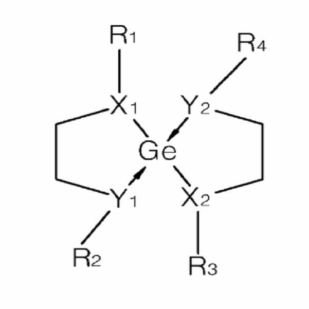
상기 Ge(Ⅱ) 소오스는 아미드 리간드(amide ligand) 포스파니도 리간드(phosphanido ligand), 알콕사이드 리간드(alkoxide ligand), 또는 티올레이트 리간드(thiolate ligand)를 포함할 수 있다. 구체적으로, 상기 Ge(Ⅱ) 소오스는 하기 화학식들 2 내지 4으로 표시되는 소오스들 중 어느 하나일 수 있다.The Ge (II) source may comprise an amide ligand, a phosphanido ligand, an alkoxide ligand, or a thiolate ligand. Specifically, the Ge (II) source may be any of the sources represented by the following formulas (2) to (4).
상기 화학식 2에서, X1 및 X2는 각각 독립적으로 N 또는 P이고, R1, R2, R3 및 R4는 각각 독립적으로 수소; C1 ~ C10의 알킬기(alkyl group); CH3가 이민기(imine group), 아민기(amine group), 알콕시기(alkoxy group) 또는 케톤기(ketone group)로 치환된 C1 ~ C10의 알킬기; CH3가 이민기, 아민기, 알콕시기 또는 케톤기로 치환되고, 상기 이민기의 N, 상기 아민기의 N, 상기 알콕시기의 O 또는 상기 케톤기의 O는 Ge와 배위 결합한 C1 ~ C10의 알킬기; C 2 ~ C12의 올레핀기(olefinic group); CH3가 이민기, 아민기, 알콕시기 또는 케톤기로 치환된 C3 ~ C12의 올레핀기; CH3가 이민기, 아민기, 알콕시기 또는 케톤기로 치환되고, 상기 이민기의 N, 상기 아민기의 N, 상기 알콕시기의 O 또는 상기 케톤기의 O는 Ge와 배위 결합한 C3 ~ C12의 올레핀기; C2 ~ C13의 아세틸렌기(acetylenic group); 알렌기(allenic group; CHCCH2); 시안기(cyano group; CN); NCX기(X는 O, S, Se 또는 Te); 아지드 리간드(azide ligand; N3); 아미드 리간드(amide ligand; NR5R6, R5 및 R6는 각각 독립적으로 수소, C1 ~ C10의 알킬기, C2 ~ C12의 올레핀기, C2 ~ C13의 아 세틸렌기 또는 알렌기); SiR7R8R9(R7, R8 및 R9는 각각 독립적으로 수소, C1 ~ C10의 알킬기, C2 ~ C12의 올레핀기, C2 ~ C13의 아세틸렌기 또는 알렌기); 또는 이들의 조합이거나, R1, R2, R3 및 R4중 둘 이상이 화학적으로 결합되어 고리 시스템을 형성한다.In Formula 2, X 1 And X 2 are each independently N or P, and R 1 , R 2 , R 3, and R 4 are each independently hydrogen; A C 1 to C 10 alkyl group; A C 1 -C 10 alkyl group in which CH 3 is substituted by an imine group, an amine group, an alkoxy group or a ketone group; CH 3 is substituted with an imine group, an amine group, an alkoxy group or a ketone group, N of the imine group, N of the amine group, O of the alkoxy group or O of the ketone group is a C 1 -C 10 alkyl group ; C 2 to C 12 olefinic groups; A C 3 to C 12 olefin group in which CH 3 is substituted with an imine group, an amine group, an alkoxy group or a ketone group; CH 3 is substituted with an imine group, an amine group, an alkoxy group or a ketone group, and N of the imine group, N of the amine group, O of the alkoxy group, or O of the ketone group is substituted with C 3 -C 12 olefin group; An acetylenic group of C 2 to C 13 ; Allenic group (CHCCH 2 ); A cyano group (CN); NCX group (X is O, S, Se or Te); Azide ligand (N 3 ); Amide ligand (NR 5 R 6 , R 5 and R 6 are each independently hydrogen, a C 1 to C 10 alkyl group, a C 2 to C 12 olefin group, a C 2 to C 13 acetylene group or an allene group); SiR 7 R 8 R 9 wherein R 7 , R 8 and R 9 are each independently hydrogen, a C 1 to C 10 alkyl group, a C 2 to C 12 olefin group, a C 2 to C 13 acetylene group or an allene group) ; Or a combination thereof, or two or more of R 1 , R 2 , R 3 and R 4 are chemically bonded to form a ring system.
상기 화학식 3에서, Y1 및 Y2는 각각 독립적으로 O 또는 S이고, R1 및 R2는 각각 독립적으로 수소; C1 ~ C10의 알킬기; CH3가 이민기, 아민기, 알콕시기 또는 케톤기로 치환된 C1 ~ C10의 알킬기; CH3가 이민기, 아민기, 알콕시기 또는 케톤기로 치환되고, 상기 이민기의 N, 상기 아민기의 N, 상기 알콕시기의 O 또는 상기 케톤기의 O는 Ge와 배위 결합한 C1 ~ C10의 알킬기; C 2 ~ C12의 올레핀기; CH3가 이민기, 아민기, 알콕시기 또는 케톤기로 치환된 C3 ~ C12의 올레핀기; CH3가 이민기, 아민기, 알콕시기 또는 케톤기로 치환되고, 상기 이민기의 N, 상기 아민기의 N, 상기 알콕시기의 O 또는 상기 케톤기의 O는 Ge와 배위 결합한 C3 ~ C12의 올레핀기; C2 ~ C13의 아세틸렌기; 알렌기(CHCCH2); 시안기(CN); NCX기(X는 O, S, Se 또는 Te); 아지드 리간드(N3); 아미드 리간드(NR3R4, R3 및 R4는 각각 독립적으로 수소, C1 ~ C10 의 알킬기, C2 ~ C12의 올레핀기, C2 ~ C13의 아세틸렌기 또는 알렌기); SiR5R6R7(R5, R6 및 R7는 각각 독립적으로 수소, C1 ~ C10의 알킬기, C2 ~ C12의 올레핀기, C2 ~ C13의 아세틸렌기 또는 알렌기); 또는 이들의 조합이거나, R1과 R2가 화학적으로 결합되어 고리 시스템을 형성한다.In Formula 3, Y 1 And Y < 2 > are each independently O or S, and R < 1 & And R < 2 > are each independently selected from the group consisting of hydrogen; Alkyl group of C 1 ~ C 10; A C 1 -C 10 alkyl group in which CH 3 is substituted by an imine group, an amine group, an alkoxy group or a ketone group; CH 3 is substituted with an imine group, an amine group, an alkoxy group or a ketone group, N of the imine group, N of the amine group, O of the alkoxy group or O of the ketone group is a C 1 -C 10 alkyl group ; C 2 to C 12 olefin groups; A C 3 to C 12 olefin group in which CH 3 is substituted with an imine group, an amine group, an alkoxy group or a ketone group; CH 3 is substituted with an imine group, an amine group, an alkoxy group or a ketone group, and N of the imine group, N of the amine group, O of the alkoxy group, or O of the ketone group is substituted with C 3 -C 12 olefin group; An acetylene group of C 2 to C 13 ; Allene group (CHCCH 2 ); A cyano group (CN); NCX group (X is O, S, Se or Te); Azide ligand (N 3 ); An amide ligand (NR 3 R 4 , R 3 and R 4 are each independently hydrogen, a C 1 to C 10 alkyl group, a C 2 to C 12 olefin group, a C 2 to C 13 acetylene group or an allylene group); SiR 5 R 6 R 7 wherein R 5 , R 6 and R 7 are each independently hydrogen, a C 1 to C 10 alkyl group, a C 2 to C 12 olefin group, a C 2 to C 13 acetylene group or an allene group) ; Or a combination thereof, or R 1 and R 2 are chemically bonded to form a ring system.
상기 화학식 4에서, X는 N 또는 P이고, Y는 O 또는 S이고, R1, R2 및 R3는 각각 독립적으로 수소; C1 ~ C10의 알킬기; CH3가 이민기, 아민기, 알콕시기 또는 케톤기로 치환된 C1 ~ C10의 알킬기; CH3가 이민기, 아민기, 알콕시기 또는 케톤기로 치환되고, 상기 이민기의 N, 상기 아민기의 N, 상기 알콕시기의 O 또는 상기 케톤기의 O는 Ge와 배위 결합한 C1 ~ C10의 알킬기; C 2 ~ C12의 올레핀기; CH3가 이민기, 아민기, 알콕시기 또는 케톤기로 치환된 C3 ~ C12의 올레핀기; CH3가 이민기, 아민기, 알콕시기 또는 케톤기로 치환되고, 상기 이민기의 N, 상기 아민기의 N, 상기 알콕시기의 O 또는 상기 케톤기의 O는 Ge와 배위 결합한 C3 ~ C12의 올레핀기; C2 ~ C13의 아세틸렌기; 알렌기(CHCCH2); 시안기(CN); NCX기(X는 O, S, Se 또는 Te); 아지드 리간드(N3); 아미드 리간드(NR4R5, R4 및 R5는 각각 독립적으로 수소, C1 ~ C10 의 알킬기, C2 ~ C12의 올레핀기, C2 ~ C13의 아세틸렌기 또는 알렌기); SiR6R7R8(R6, R7 및 R8는 각각 독립적으로 수소, C1 ~ C10의 알킬기, C2 ~ C12의 올레핀기, C2 ~ C13의 아세틸렌기 또는 알렌기); 또는 이들의 조합이거나, R1, R2 및 R3중 둘 이상이 화학적으로 결합되어 고리 시스템을 형성한다.In Formula 4, X is N or P, Y is O or S, R 1 , R 2, and R 3 are each independently hydrogen; Alkyl group of C 1 ~ C 10; A C 1 -C 10 alkyl group in which CH 3 is substituted by an imine group, an amine group, an alkoxy group or a ketone group; CH 3 is substituted with an imine group, an amine group, an alkoxy group or a ketone group, N of the imine group, N of the amine group, O of the alkoxy group or O of the ketone group is a C 1 -C 10 alkyl group ; C 2 to C 12 olefin groups; A C 3 to C 12 olefin group in which CH 3 is substituted with an imine group, an amine group, an alkoxy group or a ketone group; CH 3 is substituted with an imine group, an amine group, an alkoxy group or a ketone group, and N of the imine group, N of the amine group, O of the alkoxy group, or O of the ketone group is substituted with C 3 -C 12 olefin group; An acetylene group of C 2 to C 13 ; Allene group (CHCCH 2 ); A cyano group (CN); NCX group (X is O, S, Se or Te); Azide ligand (N 3 ); An amide ligand (NR 4 R 5 , R 4 and R 5 are each independently hydrogen, a C 1 to C 10 alkyl group, a C 2 to C 12 olefin group, a C 2 to C 13 acetylene group or an allene group); SiR 6 R 7 R 8 wherein R 6 , R 7 and R 8 are each independently hydrogen, a C 1 to C 10 alkyl group, a C 2 to C 12 olefin group, a C 2 to C 13 acetylene group or an allene group) ; Or a combination thereof, or R 1 , R 2 And R < 3 > are chemically bonded to form a ring system.
상기 기술적 과제를 이루기 위하여 본 발명의 일 측면은 다른 상변화 물질막 형성방법을 제공한다. 반응 챔버 내에 제1 소오스로서 Ge(Ⅱ) 소오스를 공급한다. 상기 반응 챔버 내에 제2 소오스를 공급하여 Ge 함유 상변화 물질막을 형성한다.According to an aspect of the present invention, there is provided a method of forming a phase change material layer. A Ge (II) source is supplied as a first source into the reaction chamber. A second source is supplied into the reaction chamber to form a Ge-containing phase change material film.
상기 Ge(Ⅱ) 소오스는 하기 화학식들 5 내지 17 중 어느 하나일 수 있다.The Ge (II) source may be any one of the following formulas 5 to 17.

상기 화학식 5에서, X1 및 X2는 각각 독립적으로 N 또는 P이고, R1, R2, R3 및 R4는 각각 독립적으로 수소, C1 ~ C10의 알킬기, C2 ~ C12의 올레핀기, C2 ~ C13의 아세틸렌기, 또는 알렌기이다.In Formula 5, X 1 And X 2 are each independently N or P, R 1, R 2, R 3 and R 4 are each independently hydrogen, C 1 ~ C 10 alkyl group, C 2 ~ C 12 olefin group, C 2 ~ C 13 , or an allylene group.

상기 화학식 6에서, X1 및 X2는 각각 독립적으로 N 또는 P이고, R1 및 R2는 각각 독립적으로 수소, C1 ~ C10의 알킬기, C2 ~ C12의 올레핀기, C2 ~ C13의 아세틸렌기 또는 알렌기이다.In Formula 6, X 1 And X 2 are each independently N or P and R 1 and R 2 are each independently selected from the group consisting of hydrogen, a C 1 to C 10 alkyl group, a C 2 to C 12 olefin group, a C 2 to C 13 acetylene group, .

상기 화학식 7에서, X1, X2, X3 및 X4는 각각 독립적으로 N 또는 P이고, R1, R2, R3, R4, R5 및 R6은 각각 독립적으로 수소, C1 ~ C10의 알킬기, C2 ~ C12의 올레핀기, C2 ~ C13의 아세틸렌기 또는 알렌기이다.Wherein X 1 , X 2 , X 3 and X 4 are each independently N or P and R 1 , R 2 , R 3 , R 4 , R 5 And R 6 are each independently hydrogen, a C 1 to C 10 alkyl group, a C 2 to C 12 olefin group, a C 2 to C 13 acetylene group, or an allene group.

상기 화학식 8에서, X1 및 X2는 각각 독립적으로 N 또는 P이고, Y1 및 Y2는 각각 독립적으로 O 또는 S이고, R1, R2, R3, R4, R5, R6, R7 및 R8은 각각 독립적으로 수소, C1 ~ C10의 알킬기, C2 ~ C12의 올레핀기, C2 ~ C13의 아세틸렌기 또는 알렌기이다.In Formula 8, X 1 and X 2 are each independently N or P, and, Y 1 and Y 2 are each independently O or S, R 1, R 2, R 3, R 4, R 5, R 6 , R 7 and R 8 are each independently hydrogen, a C 1 to C 10 alkyl group, a C 2 to C 12 olefin group, a C 2 to C 13 acetylene group or an allene group.

상기 화학식 9에서, X1, X2, X3 및 X4는 각각 독립적으로 N 또는 P이고, R1, R2, R3, R4, R5, R6, R7, R8, R9 및 R10은 각각 독립적으로 수소, C1 ~ C10의 알킬기, C2 ~ C12의 올레핀기, C2 ~ C13의 아세틸렌기 또는 알렌기이다.Wherein X 1 , X 2 , X 3 and X 4 are each independently N or P and R 1 , R 2 , R 3 , R 4 , R 5 , R 6 , R 7 , R 8 , R 9 and R 10 are each independently hydrogen, a C 1 to C 10 alkyl group, a C 2 to C 12 olefin group, a C 2 to C 13 acetylene group, or an allene group.

상기 화학식 10에서, X1, X2, X3 및 X4는 각각 독립적으로 N 또는 P이고, R1, R2, R3, R4, R5 및 R6은 각각 독립적으로 수소, C1 ~ C10의 알킬기, C2 ~ C12의 올레핀기, C2 ~ C13의 아세틸렌기 또는 알렌기이다.In Formula 10, X 1, X 2, X 3 and X 4 are each independently N or P, R 1, R 2, R 3, R 4, R 5 and R 6 are independently hydrogen, C 1 each An alkyl group having 1 to 10 carbon atoms, an olefin group having 2 to 12 carbon atoms, an acetylene group or an allene group having 2 to 13 carbon atoms.

상기 화학식 11에서, X1 및 X2는 각각 독립적으로 N 또는 P이고, Y1 및 Y2는 각각 독립적으로 O 또는 S이고, R1, R2, R3 및 R4은 각각 독립적으로 수소, C1 ~ C10의 알킬기, C2 ~ C12의 올레핀기, C2 ~ C13의 아세틸렌기 또는 알렌기이다.In Formula 11, X 1 and X 2 are each independently N or P, Y 1 and Y 2 are each independently O or S, R 1 , R 2 , R 3 and R 4 are each independently hydrogen, A C 1 to C 10 alkyl group, a C 2 to C 12 olefin group, a C 2 to C 13 acetylene group, or an allylene group.

상기 화학식 12에서, Y1 및 Y2는 각각 독립적으로 O 또는 S이고, R1 및 R2은 각각 독립적으로 수소, C1 ~ C10의 알킬기, C2 ~ C12의 올레핀기, C2 ~ C13의 아세틸렌기 또는 알렌기이다.In Formula 12, Y 1 and Y 2 are each independently O or S, R 1 and R 2 are each independently hydrogen, C 1 ~ C 10 alkyl group, C 2 ~ C 12 olefin group, C 2 ~ of An acetylene group or an allylene group of C < 13 >

상기 화학식 13에서, Y1 및 Y2는 각각 독립적으로 O 또는 S이고, R1 및 R2은 각각 독립적으로 수소, C1 ~ C10의 알킬기, C2 ~ C12의 올레핀기, C2 ~ C13의 아세틸렌기 또는 알렌기이다.In Formula 13, Y 1 and Y 2 are each independently O or S, R 1 and R 2 are each independently hydrogen, C 1 ~ C 10 alkyl group, C 2 ~ C 12 olefin group, C 2 ~ of An acetylene group or an allylene group of C < 13 >

상기 화학식 14에서, Y1, Y2, Y3 및 Y4는 각각 독립적으로 O 또는 S이고, R1, R2, R3, R4, R5 및 R6은 각각 독립적으로 수소, C1 ~ C10의 알킬기, C2 ~ C12의 올레핀기, C2 ~ C13의 아세틸렌기 또는 알렌기이다.In Formula 14, Y 1, Y 2, Y 3 and Y 4 are each independently O or S, R 1, R 2, R 3, R 4, R 5 and R 6 is hydrogen, C 1 are each independently An alkyl group having 1 to 10 carbon atoms, an olefin group having 2 to 12 carbon atoms, an acetylene group or an allene group having 2 to 13 carbon atoms.

상기 화학식 15에서, X1 및 X2는 각각 독립적으로 N 또는 P이고, Y1 및 Y2는 각각 독립적으로 O 또는 S이고, R1, R2, R3 및 R4은 각각 독립적으로 수소, C1 ~ C10의 알킬기, C2 ~ C12의 올레핀기, C2 ~ C13의 아세틸렌기 또는 알렌기이다.In Formula 15, X 1 and X 2 are each independently N or P, Y 1 and Y 2 are each independently O or S, and R 1 , R 2 , R 3, and R 4 are each independently hydrogen, A C 1 to C 10 alkyl group, a C 2 to C 12 olefin group, a C 2 to C 13 acetylene group, or an allylene group.

상기 화학식 16에서, Y1, Y2, Y3 및 Y4는 각각 독립적으로 O 또는 S이고,R1 및 R2은 각각 독립적으로 수소, C1 ~ C10의 알킬기, C2 ~ C12의 올레핀기, C2 ~ C13의 아세틸렌기 또는 알렌기이다.Y 1 , Y 2 , Y 3 and Y 4 are each independently O or S, R 1 and R 2 are each independently hydrogen, a C 1 to C 10 alkyl group, a C 2 to C 12 An olefin group, an acetylene group or an allene group of C 2 to C 13 .

상기 화학식 17에서, X는 N 또는 P이고, Y는 O 또는 S이고, R1, R2 및 R3은 각각 독립적으로 수소, C1 ~ C10의 알킬기, C2 ~ C12의 올레핀기, C2 ~ C13의 아세틸렌기 또는 알렌기이다.Wherein X is N or P, Y is O or S, R 1 , R 2 and R 3 are each independently hydrogen, a C 1 to C 10 alkyl group, a C 2 to C 12 olefin group, An acetylene group or an allylene group of C 2 to C 13 .
상기 기술적 과제를 이루기 위하여 본 발명의 다른 측면은 상변화 메모리 소 자 제조방법을 제공한다. 반응 챔버 내에 하부 전극이 형성된 기판을 로딩한다. 상기 기판이 로딩된 반응 챔버 내에 화학식 1로 표시되는 반응 기체, 제1 소오스인 Ge(Ⅱ) 소오스 및 제2 소오스를 공급하여 상기 하부 전극 상에 Ge 함유 상변화 물질막을 형성한다. 상기 상변화 물질막 상에 상부 전극을 형성한다.According to another aspect of the present invention, there is provided a method for fabricating a phase change memory device. The substrate on which the lower electrode is formed is loaded in the reaction chamber. A Ge-containing phase change material film is formed on the lower electrode by supplying a reaction gas represented by the formula (1), a first source Ge (II) source and a second source into the reaction chamber loaded with the substrate. An upper electrode is formed on the phase change material film.
상기 상변화 물질막을 형성하기 전에, 상기 하부 전극 상에 상기 하부 전극의 일부를 노출시키는 비아홀을 갖는 몰드 절연막을 형성할 수 있다. 이 경우에, 상기 상변화 물질막은 상기 비아홀 내에 형성할 수 있다. Before forming the phase change material layer, a mold insulating layer having a via hole exposing a part of the lower electrode may be formed on the lower electrode. In this case, the phase change material film can be formed in the via hole.
일 실시예에서, 상기 상변화 물질막은 상기 비아홀을 채울 수 있다.In one embodiment, the phase change material film may fill the via hole.
다른 실시예에서, 상기 상변화 물질막은 상기 비아홀의 측벽 상에 형성할 수 있다. 상기 상변화 물질막을 이방성 식각하여 상기 비아홀의 측벽 상에 상변화 물질 스페이서를 형성하고, 상기 상변화 물질 스페이서가 형성된 비아홀 내에 버퍼 절연막을 채우고, 상기 상변화 물질 스페이서의 상부면이 노출될 때까지 상기 버퍼 절연막을 평탄화 식각할 수 있다. 이 경우에, 상기 상부 전극은 상기 상변화 물질 스페이서 상에 형성할 수 있다.In another embodiment, the phase change material film may be formed on the side wall of the via hole. Anisotropically etching the phase change material layer to form a phase change material spacer on a sidewall of the via hole; filling a buffer insulation layer in a via hole formed with the phase change material spacer; The buffer insulating film can be planarized and etched. In this case, the upper electrode may be formed on the phase change material spacer.
상술한 바와 같이 본 발명에 따르면, 첫째로, Ge(Ⅱ) 소오스는 Ge(Ⅳ) 소오스에 비해 반응성이 향상되어, 상변화 물질막을 형성할 때의 증착 온도를 감소시킬 수 있다. 이러한 낮은 온도에서 증착된 상변화 물질막은 높은 공정온도에서 형성된 상변화 물질막에 비해 그레인 사이즈가 작다. 따라서, 상변화 물질막의 스텝 커버리지가 향상되어 콘택홀의 입구를 막지 않으면서 콘택홀의 측벽 상에 콘포말한 상 변화 물질막을 형성할 수 있으며, 나아가 콘택홀을 보이드 없이 채울 수 있다. As described above, according to the present invention, firstly, the Ge (II) source has improved reactivity as compared with the Ge (IV) source, and can reduce the deposition temperature when forming the phase change material film. The phase change material film deposited at such a low temperature has a smaller grain size than the phase change material film formed at a high processing temperature. Therefore, the step coverage of the phase change material film is improved, so that the phase change material film can be formed on the side wall of the contact hole without blocking the entrance of the contact hole, and the contact hole can be filled without voids.
둘째로, NR1R2R3 (여기서, R1, R2 및 R3는 각각 독립적으로 H, CH3, C2H5, C3H7, C4H9, Si(CH3)3, NH2, NH(CH3), N(CH3)2, NH(C2H5) 또는 N(C2H5)2임)로 표시되는 반응 기체를 사용함으로써, 상기 반응 기체와 Ge(Ⅱ) 소오스와의 반응성을 향상시켜 상변화 물질막의 증착 속도를 향상시킬 수 있다.Second, NR 1 R 2 R 3 , wherein R 1 , R 2 And R 3 are each independently H, CH 3, C 2 H 5, C 3 H 7, C 4 H 9, Si (CH 3) 3, NH 2, NH (CH 3), N (CH 3) 2, NH (C 2 H 5 ) or N (C 2 H 5 ) 2 ), the reactivity between the reactive gas and the Ge (Ⅱ) source is improved to improve the deposition rate of the phase change material film .
이하, 첨부한 도면들을 참조하여 본 발명의 바람직한 실시예들을 상세히 설명한다. 그러나, 본 발명은 여기서 설명되는 실시예들에 한정되지 않고 다른 형태로 구체화될 수도 있다. 오히려, 여기서 소개되는 실시예들은 개시된 내용이 철저하고 완전해질 수 있도록 그리고 당업자에게 본 발명의 사상이 충분히 전달될 수 있도록 하기 위해 제공되는 것이다. 도면들에 있어서, 층 및 영역들의 두께는 명확성을 기하여 위하여 과장된 것이다. 명세서 전체에 걸쳐서 동일한 참조번호들은 동일한 구성요소들을 나타낸다.Hereinafter, preferred embodiments of the present invention will be described in detail with reference to the accompanying drawings. However, the present invention is not limited to the embodiments described herein but may be embodied in other forms. Rather, the embodiments disclosed herein are provided so that the disclosure can be thorough and complete, and will fully convey the scope of the invention to those skilled in the art. In the drawings, the thicknesses of the layers and regions are exaggerated for clarity. Like reference numerals designate like elements throughout the specification.
상변화Phase change 물질막Material film 형성 방법 How to form
도 2는 본 발명의 일 실시예에 따른 상변화 물질막 형성 방법을 나타낸 플로우 챠트(flow chart)이다.2 is a flow chart illustrating a method of forming a phase change material film according to an embodiment of the present invention.
도 2를 참조하면, 반응 챔버 내에 기판을 로딩한다(S10). 상기 기판은 실리콘 산화물, 티타늄 산화물, 알루미늄 산화물(Al2O3), 지르코늄 산화물 또는 하프늄 산화물로 이루어진 유전막; 티타늄(Ti), 티타늄 질화물(TiN), 알루미늄, 탈륨(Ta), 탈륨 질화물(TaN) 또는 티타늄 알루미늄 질화물(TiAlN)로 이루어진 도전막; 또는 실리콘 또는 실리콘 카바이드(SiC)로 이루어진 반도체막을 포함할 수 있다. Referring to FIG. 2, a substrate is loaded in a reaction chamber (S10). Wherein the substrate is a dielectric film made of silicon oxide, titanium oxide, aluminum oxide (Al2O3), zirconium oxide, or hafnium oxide; A conductive film made of titanium (Ti), titanium nitride (TiN), aluminum, thallium (Ta), thallium nitride (TaN), or titanium aluminum nitride (TiAlN); Or a semiconductor film made of silicon or silicon carbide (SiC).
상기 반응 챔버는 냉벽형(cold wall type) 또는 열벽형(hot wall type)일 수 있다. 상기 냉벽형 반응 챔버는 열선이 구비된 기판 스테이지 및 상기 기판 스테이지 상에 위치하는 샤워 헤드를 구비할 수 있다. 상기 기판 스테이지 상에 상기 기판이 배치될 수 있다. 이러한 냉벽형 반응 챔버는 매엽식(single type)일 수 있다. 한편, 열벽형 반응 챔버는 그의 벽 내에 열선이 배치된다. 상기 열벽형 반응 챔버 내에 다수 장의 기판이 수직으로 적층될 수 있다. 이러한 반응 챔버는 수직형 & 배치식(vertical & batch type)일 수 있다.The reaction chamber may be a cold wall type or a hot wall type. The cold-walled reaction chamber may include a substrate stage having a heating wire and a showerhead positioned on the substrate stage. The substrate may be disposed on the substrate stage. The cold wall type reaction chamber may be a single type. On the other hand, the thermal wall type reaction chamber has a heat line disposed in its wall. A plurality of substrates may be vertically stacked in the thermal-walled reaction chamber. Such a reaction chamber may be a vertical & batch type.
상기 반응 챔버 내에 하기 화학식 1로 표시되는 반응 기체를 공급할 수 있다(S20).A reaction gas represented by the following formula (1) may be fed into the reaction chamber (S20).
<화학식 1>≪
NR1R2R3 NR 1 R 2 R 3
상기 화학식 1에서, R1, R2 및 R3는 각각 독립적으로 H, CH3, C2H5, C3H7, C4H9,Si(CH3)3, NH2, NH(CH3), N(CH3)2, NH(C2H5) 또는 N(C2H5)2이다.In
상기 반응 기체는 NH2기를 구비하는 반응 기체일 수 있다. 나아가, 상기 반응 기체는 암모니아(ammonia), 1차 아민(primary amine) 및 하이드라진(hydrazine)으로 이루어진 군에서 선택되는 하나의 기체일 수 있다. 상기 반응 기체를 공급하기 전, 후 또는 이와 동시에 상기 반응 챔버 내에 제1 소오스로서 Ge(Ⅱ) 소오스를 공급할 수 있다(S30). Ge(Ⅱ) 소오스에서 "Ⅱ"는 Ge의 산화 상태(oxidation state)가 +2인 것을 의미한다. 상기 Ge(Ⅱ) 소오스는 운반 기체와 함께 공급할 수 있다. 상기 운반 기체는 불활성 기체로서 아르곤(Ar), 헬륨(He) 또는 질소(N2)를 함유할 수 있다. 이와는 달리, 상기 Ge(Ⅱ) 소오스를 용매를 사용하여 녹인 후 기화기에서 급속하게 기체로 기화시켜 상기 반응 챔버 내에 공급할 수 있다.The reactive gas may be a reactive gas having an NH 2 group. Further, the reaction gas may be one gas selected from the group consisting of ammonia, primary amine, and hydrazine. The Ge (II) source may be supplied as the first source into the reaction chamber before, after, or simultaneously with the supply of the reactive gas (S30). In the Ge (II) source, "II" means that the oxidation state of Ge is +2. The Ge (II) source can be supplied with the carrier gas. The carrier gas may contain argon (Ar), helium (He) or nitrogen (N 2 ) as an inert gas. Alternatively, the Ge (II) source may be dissolved using a solvent, and then vaporized rapidly in a vaporizer to be supplied into the reaction chamber.
상기 Ge(Ⅱ) 소오스는 아미드 리간드(amide ligand), 포스파니도 리간드(phosphanido ligand), 알콕사이드 리간드(alkoxide ligand), 또는 티올레이트 리간드(thiolate ligand)를 구비할 수 있다.The Ge (II) source may have an amide ligand, a phosphanido ligand, an alkoxide ligand, or a thiolate ligand.
아미드 리간드 및/또는 포스파니도 리간드를 구비하는 Ge(Ⅱ) 소오스는 하기 화학식 2로 표시될 수 있다.The Ge (II) source having an amide ligand and / or a phosphandido ligand can be represented by the following formula (2).
<화학식 2>(2)
R1R2X1-Ge- X2R3R4 R 1 R 2 X 1 -Ge- X 2 R 3 R 4
상기 화학식 2에서, X1 및 X2는 각각 독립적으로 N 또는 P이고, R1, R2, R3 및 R4는 각각 독립적으로 수소; C1 ~ C10의 알킬기(alkyl group); CH3가 이민기(imine group), 아민기(amine group), 알콕시기(alkoxy group) 또는 케톤기(ketone group)로 치환된 C1 ~ C10의 알킬기; CH3가 이민기, 아민기, 알콕시기 또는 케톤기로 치환되고, 상기 이민기의 N, 상기 아민기의 N, 상기 알콕시기의 O 또는 상기 케톤기의 O는 Ge와 배위 결합한 C1 ~ C10의 알킬기; C 2 ~ C12의 올레핀 기(olefinic group); CH3가 이민기, 아민기, 알콕시기 또는 케톤기로 치환된 C3 ~ C12의 올레핀기; CH3가 이민기, 아민기, 알콕시기 또는 케톤기로 치환되고, 상기 이민기의 N, 상기 아민기의 N, 상기 알콕시기의 O 또는 상기 케톤기의 O는 Ge와 배위 결합한 C3 ~ C12의 올레핀기; C2 ~ C13의 아세틸렌기(acetylenic group); 알렌기(allenic group; CHCCH2); 시안기(cyano group; CN); NCX기(X는 O, S, Se 또는 Te); 아지드 리간드(azide ligand; N3); 아미드 리간드(amide ligand; NR5R6, R5 및 R6는 각각 독립적으로 수소, C1 ~ C10의 알킬기, C2 ~ C12의 올레핀기, C2 ~ C13의 아세틸렌기 또는 알렌기); SiR7R8R9(R7, R8 및 R9는 각각 독립적으로 수소, C1 ~ C10의 알킬기, C2 ~ C12의 올레핀기, C2 ~ C13의 아세틸렌기 또는 알렌기); 또는 이들의 조합이거나, R1, R2, R3 및 R4중 둘 이상이 화학적으로 결합되어 고리 시스템을 형성한다.In Formula 2, X 1 And X 2 are each independently N or P, and R 1 , R 2 , R 3, and R 4 are each independently hydrogen; A C 1 to C 10 alkyl group; A C 1 -C 10 alkyl group in which CH 3 is substituted by an imine group, an amine group, an alkoxy group or a ketone group; CH 3 is substituted with an imine group, an amine group, an alkoxy group or a ketone group, N of the imine group, N of the amine group, O of the alkoxy group or O of the ketone group is a C 1 -C 10 alkyl group ; C 2 to C 12 olefinic groups; A C 3 to C 12 olefin group in which CH 3 is substituted with an imine group, an amine group, an alkoxy group or a ketone group; CH 3 is substituted with an imine group, an amine group, an alkoxy group or a ketone group, and N of the imine group, N of the amine group, O of the alkoxy group, or O of the ketone group is substituted with C 3 -C 12 olefin group; An acetylenic group of C 2 to C 13 ; Allenic group (CHCCH 2 ); A cyano group (CN); NCX group (X is O, S, Se or Te); Azide ligand (N 3 ); Amide ligand wherein each of NR 5 R 6 , R 5 and R 6 is independently hydrogen, a C 1 to C 10 alkyl group, a C 2 to C 12 olefin group, a C 2 to C 13 acetylene group or an allene group ); SiR 7 R 8 R 9 wherein R 7 , R 8 and R 9 are each independently hydrogen, a C 1 to C 10 alkyl group, a C 2 to C 12 olefin group, a C 2 to C 13 acetylene group or an allene group) ; Or a combination thereof, or two or more of R 1 , R 2 , R 3 and R 4 are chemically bonded to form a ring system.
알콕사이드 리간드 및/또는 티올레이트 리간드를 구비하는 Ge(Ⅱ) 소오스는 하기 화학식 3으로 표시될 수 있다.A Ge (II) source having an alkoxide ligand and / or a thiolate ligand can be represented by the following formula (3).
<화학식 3>(3)
R1Y1-Ge-Y2R2 R 1 is Y 1 -Ge-Y 2 R 2
상기 화학식 3에서, Y1 및 Y2는 각각 독립적으로 O 또는 S이고, R1 및 R2는 각각 독립적으로 수소; C1 ~ C10의 알킬기; CH3가 이민기, 아민기, 알콕시기 또는 케톤기로 치환된 C1 ~ C10의 알킬기; CH3가 이민기, 아민기, 알콕시기 또는 케톤기로 치환되고, 상기 이민기의 N, 상기 아민기의 N, 상기 알콕시기의 O 또는 상기 케톤기의 O는 Ge와 배위 결합한 C1 ~ C10의 알킬기; C 2 ~ C12의 올레핀기; CH3가 이민기, 아민기, 알콕시기 또는 케톤기로 치환된 C3 ~ C12의 올레핀기; CH3가 이민기, 아민기, 알콕시기 또는 케톤기로 치환되고, 상기 이민기의 N, 상기 아민기의 N, 상기 알콕시기의 O 또는 상기 케톤기의 O는 Ge와 배위 결합한 C3 ~ C12의 올레핀기; C2 ~ C13의 아세틸렌기; 알렌기(CHCCH2); 시안기(CN); NCX기(X는 O, S, Se 또는 Te); 아지드 리간드(N3); 아미드 리간드(NR3R4, R3 및 R4는 각각 독립적으로 수소, C1 ~ C10의 알킬기, C2 ~ C12의 올레핀기, C2 ~ C13의 아세틸렌기 또는 알렌기); SiR5R6R7(R5, R6 및 R7는 각각 독립적으로 수소, C1 ~ C10의 알킬기, C2 ~ C12의 올레핀기, C2 ~ C13의 아세틸렌기 또는 알렌기); 또는 이들의 조합이거나, R1과 R2가 화학적으로 결합되어 고리 시스템을 형성한다.In Formula 3, Y 1 And Y < 2 > are each independently O or S, and R < 1 & And R < 2 > are each independently selected from the group consisting of hydrogen; Alkyl group of C 1 ~ C 10; A C 1 -C 10 alkyl group in which CH 3 is substituted by an imine group, an amine group, an alkoxy group or a ketone group; CH 3 is substituted with an imine group, an amine group, an alkoxy group or a ketone group, N of the imine group, N of the amine group, O of the alkoxy group or O of the ketone group is a C 1 -C 10 alkyl group ; C 2 to C 12 olefin groups; A C 3 to C 12 olefin group in which CH 3 is substituted with an imine group, an amine group, an alkoxy group or a ketone group; CH 3 is substituted with an imine group, an amine group, an alkoxy group or a ketone group, and N of the imine group, N of the amine group, O of the alkoxy group, or O of the ketone group is substituted with C 3 -C 12 olefin group; An acetylene group of C 2 to C 13 ; Allene group (CHCCH 2 ); A cyano group (CN); NCX group (X is O, S, Se or Te); Azide ligand (N 3 ); An amide ligand (NR 3 R 4 , R 3 and R 4 are each independently hydrogen, a C 1 to C 10 alkyl group, a C 2 to C 12 olefin group, a C 2 to C 13 acetylene group or an allylene group); SiR 5 R 6 R 7 wherein R 5 , R 6 and R 7 are each independently hydrogen, a C 1 to C 10 alkyl group, a C 2 to C 12 olefin group, a C 2 to C 13 acetylene group or an allene group) ; Or a combination thereof, or R 1 and R 2 are chemically bonded to form a ring system.
아미드 리간드와 포스파니도 리간드 중 어느 하나; 및 알콕사이드 리간드와 티올레이트 리간드 중 어느 하나를 구비하는 Ge(Ⅱ) 소오스는 하기 화학식 4으로 표시될 수 있다.Amide ligand and phosphandido ligand; And a Ge (II) source having any one of an alkoxide ligand and a thiolate ligand can be represented by the following general formula (4).
<화학식 4>≪ Formula 4 >
R1R2X-Ge-YR3 R 1 R 2 X-Ge-YR 3
상기 화학식 4에서, X는 N 또는 P이고, Y는 O 또는 S이고, R1, R2 및 R3는 각각 독립적으로 수소; C1 ~ C10의 알킬기; CH3가 이민기, 아민기, 알콕시기 또는 케톤기로 치환된 C1 ~ C10의 알킬기; CH3가 이민기, 아민기, 알콕시기 또는 케톤기로 치환되고, 상기 이민기의 N, 상기 아민기의 N, 상기 알콕시기의 O 또는 상기 케톤기의 O는 Ge와 배위 결합한 C1 ~ C10의 알킬기; C 2 ~ C12의 올레핀기; CH3가 이민기, 아민기, 알콕시기 또는 케톤기로 치환된 C3 ~ C12의 올레핀기; CH3가 이민기, 아민기, 알콕시기 또는 케톤기로 치환되고, 상기 이민기의 N, 상기 아민기의 N, 상기 알콕시기의 O 또는 상기 케톤기의 O는 Ge와 배위 결합한 C3 ~ C12의 올레핀기; C2 ~ C13의 아세틸렌기; 알렌기(CHCCH2); 시안기(CN); NCX기(X는 O, S, Se 또는 Te); 아지드 리간드(N3); 아미드 리간드(NR4R5, R4 및 R5는 각각 독립적으로 수소, C1 ~ C10의 알킬기, C2 ~ C12의 올레핀기, C2 ~ C13의 아세틸렌기 또는 알렌기); SiR6R7R8(R6, R7 및 R8는 각각 독립적으로 수소, C1 ~ C10의 알킬기, C2 ~ C12의 올레핀기, C2 ~ C13의 아세틸렌기 또는 알렌기); 또는 이들의 조합이거나, R1, R2 및 R3중 둘 이상이 화학적으로 결합되어 고리 시스템을 형성한다.In Formula 4, X is N or P, Y is O or S, R 1 , R 2, and R 3 are each independently hydrogen; Alkyl group of C 1 ~ C 10; A C 1 -C 10 alkyl group in which CH 3 is substituted by an imine group, an amine group, an alkoxy group or a ketone group; CH 3 is substituted with an imine group, an amine group, an alkoxy group or a ketone group, N of the imine group, N of the amine group, O of the alkoxy group or O of the ketone group is a C 1 -C 10 alkyl group ; C 2 to C 12 olefin groups; A C 3 to C 12 olefin group in which CH 3 is substituted with an imine group, an amine group, an alkoxy group or a ketone group; CH 3 is substituted with an imine group, an amine group, an alkoxy group or a ketone group, and N of the imine group, N of the amine group, O of the alkoxy group, or O of the ketone group is substituted with C 3 -C 12 olefin group; An acetylene group of C 2 to C 13 ; Allene group (CHCCH 2 ); A cyano group (CN); NCX group (X is O, S, Se or Te); Azide ligand (N 3 ); An amide ligand (NR 4 R 5 , R 4 and R 5 are each independently hydrogen, a C 1 to C 10 alkyl group, a C 2 to C 12 olefin group, a C 2 to C 13 acetylene group or an allene group); SiR 6 R 7 R 8 wherein R 6 , R 7 and R 8 are each independently hydrogen, a C 1 to C 10 alkyl group, a C 2 to C 12 olefin group, a C 2 to C 13 acetylene group or an allene group) ; Or a combination thereof, or R 1 , R 2 And R < 3 > are chemically bonded to form a ring system.
상기 화학식 2로 표시되는 Ge(Ⅱ) 소오스에 대한 구체적인 예들은 하기 화 학식들 5 내지 11로 표시되는 Ge(Ⅱ) 소오스일 수 있다.Specific examples of the Ge (II) source represented by the formula (2) may be a Ge (II) source represented by the following chemical formulas 5 to 11.
<화학식 5>≪ Formula 5 >

상기 화학식 5에서, X1 및 X2는 각각 독립적으로 N 또는 P이고, R1, R2, R3 및 R4는 각각 독립적으로 수소, C1 ~ C10의 알킬기, C2 ~ C12의 올레핀기, C2 ~ C13의 아세틸렌기 또는 알렌기이다.In Formula 5, X 1 And X 2 are each independently N or P, R 1, R 2, R 3 and R 4 are each independently hydrogen, C 1 ~ C 10 alkyl group, C 2 ~ C 12 olefin group, C 2 ~ C 13 < / RTI >
<화학식 6>(6)

상기 화학식 6에서, X1 및 X2는 각각 독립적으로 N 또는 P이고, R1 및 R2는 각각 독립적으로 수소, C1 ~ C10의 알킬기, C2 ~ C12의 올레핀기, C2 ~ C13의 아세틸렌기 또는 알렌기이다.In Formula 6, X 1 And X 2 are each independently N or P and R 1 and R 2 are each independently selected from the group consisting of hydrogen, a C 1 to C 10 alkyl group, a C 2 to C 12 olefin group, a C 2 to C 13 acetylene group, .
<화학식 7>≪ Formula 7 >

상기 화학식 7에서, X1, X2, X3 및 X4는 각각 독립적으로 N 또는 P이고, R1, R2, R3, R4, R5 및 R6은 각각 독립적으로 수소, C1 ~ C10의 알킬기, C2 ~ C12의 올레핀기, C2 ~ C13의 아세틸렌기 또는 알렌기이다.Wherein X 1 , X 2 , X 3 and X 4 are each independently N or P and R 1 , R 2 , R 3 , R 4 , R 5 And R 6 are each independently hydrogen, a C 1 to C 10 alkyl group, a C 2 to C 12 olefin group, a C 2 to C 13 acetylene group, or an allene group.
<화학식 8>(8)

상기 화학식 8에서, X1 및 X2는 각각 독립적으로 N 또는 P이고, Y1 및 Y2는 각각 독립적으로 O 또는 S이고, R1, R2, R3, R4, R5, R6, R7 및 R8은 각각 독립적으로 수소, C1 ~ C10의 알킬기, C2 ~ C12의 올레핀기, C2 ~ C13의 아세틸렌기 또는 알렌기이 다.In Formula 8, X 1 and X 2 are each independently N or P, and, Y 1 and Y 2 are each independently O or S, R 1, R 2, R 3, R 4, R 5, R 6 , R 7 and R 8 are each independently hydrogen, a C 1 to C 10 alkyl group, a C 2 to C 12 olefin group, a C 2 to C 13 acetylene group or an allene group.
<화학식 9>≪ Formula 9 >

상기 화학식 9에서, X1, X2, X3 및 X4는 각각 독립적으로 N 또는 P이고, R1, R2, R3, R4, R5, R6, R7, R8, R9 및 R10은 각각 독립적으로 수소, C1 ~ C10의 알킬기, C2 ~ C12의 올레핀기, C2 ~ C13의 아세틸렌기 또는 알렌기이다.Wherein X 1 , X 2 , X 3 and X 4 are each independently N or P and R 1 , R 2 , R 3 , R 4 , R 5 , R 6 , R 7 , R 8 , R 9 and R 10 are each independently hydrogen, a C 1 to C 10 alkyl group, a C 2 to C 12 olefin group, a C 2 to C 13 acetylene group, or an allene group.
<화학식 10>≪

상기 화학식 10에서, X1, X2, X3 및 X4는 각각 독립적으로 N 또는 P이고, R1, R2, R3, R4, R5 및 R6은 각각 독립적으로 수소, C1 ~ C10의 알킬기, C2 ~ C12의 올레핀기, C2 ~ C13의 아세틸렌기 또는 알렌기이다.In Formula 10, X 1, X 2, X 3 and X 4 are each independently N or P, R 1, R 2, R 3, R 4, R 5 and R 6 are independently hydrogen, C 1 each An alkyl group having 1 to 10 carbon atoms, an olefin group having 2 to 12 carbon atoms, an acetylene group or an allene group having 2 to 13 carbon atoms.
<화학식 11>≪ Formula 11 >
상기 화학식 11에서, X1 및 X2는 각각 독립적으로 N 또는 P이고, Y1 및 Y2는 각각 독립적으로 O 또는 S이고, R1, R2, R3 및 R4은 각각 독립적으로 수소, C1 ~ C10의 알킬기, C2 ~ C12의 올레핀기, C2 ~ C13의 아세틸렌기 또는 알렌기이다.In Formula 11, X 1 and X 2 are each independently N or P, Y 1 and Y 2 are each independently O or S, R 1 , R 2 , R 3 and R 4 are each independently hydrogen, A C 1 to C 10 alkyl group, a C 2 to C 12 olefin group, a C 2 to C 13 acetylene group, or an allylene group.
상기 화학식 3로 표시되는 Ge(Ⅱ) 소오스에 대한 구체적인 예들은 하기 화학식들 12 내지 16로 표시되는 Ge(Ⅱ) 소오스일 수 있다.Specific examples of the Ge (II) source represented by the formula (3) may be Ge (II) source represented by the following formulas 12 to 16.
<화학식 12>≪ Formula 12 >

상기 화학식 12에서, Y1 및 Y2는 각각 독립적으로 O 또는 S이고, R1 및 R2은 각각 독립적으로 수소, C1 ~ C10의 알킬기, C2 ~ C12의 올레핀기, C2 ~ C13의 아세틸렌기 또는 알렌기이다.In Formula 12, Y 1 and Y 2 are each independently O or S, R 1 and R 2 are each independently hydrogen, C 1 ~ C 10 alkyl group, C 2 ~ C 12 olefin group, C 2 ~ of An acetylene group or an allylene group of C < 13 >
<화학식 13>≪ Formula 13 >

상기 화학식 13에서, Y1 및 Y2는 각각 독립적으로 O 또는 S이고, R1 및 R2은 각각 독립적으로 수소, C1 ~ C10의 알킬기, C2 ~ C12의 올레핀기, C2 ~ C13의 아세틸렌기 또는 알렌기이다.In Formula 13, Y 1 and Y 2 are each independently O or S, R 1 and R 2 are each independently hydrogen, C 1 ~ C 10 alkyl group, C 2 ~ C 12 olefin group, C 2 ~ of An acetylene group or an allylene group of C < 13 >
<화학식 14>≪ Formula 14 >

상기 화학식 14에서, Y1, Y2, Y3 및 Y4는 각각 독립적으로 O 또는 S이고, R1, R2, R3, R4, R5 및 R6은 각각 독립적으로 수소, C1 ~ C10의 알킬기, C2 ~ C12의 올레핀 기, C2 ~ C13의 아세틸렌기 또는 알렌기이다.In Formula 14, Y 1, Y 2, Y 3 and Y 4 are each independently O or S, R 1, R 2, R 3, R 4, R 5 and R 6 is hydrogen, C 1 are each independently An alkyl group having 1 to 10 carbon atoms, an olefin group having 2 to 12 carbon atoms, an acetylene group or an allene group having 2 to 13 carbon atoms.
<화학식 15>≪ Formula 15 >

상기 화학식 15에서, X1 및 X2는 각각 독립적으로 N 또는 P이고, Y1 및 Y2는 각각 독립적으로 O 또는 S이고, R1, R2, R3 및 R4은 각각 독립적으로 수소, C1 ~ C10의 알킬기, C2 ~ C12의 올레핀기, C2 ~ C13의 아세틸렌기 또는 알렌기이다.In Formula 15, X 1 and X 2 are each independently N or P, Y 1 and Y 2 are each independently O or S, and R 1 , R 2 , R 3, and R 4 are each independently hydrogen, A C 1 to C 10 alkyl group, a C 2 to C 12 olefin group, a C 2 to C 13 acetylene group, or an allylene group.
<화학식 16>≪

상기 화학식 16에서, Y1, Y2, Y3 및 Y4는 각각 독립적으로 O 또는 S이고, R1 및 R2은 각각 독립적으로 수소, C1 ~ C10의 알킬기, C2 ~ C12의 올레핀기, C2 ~ C13의 아세틸렌기 또는 알렌기이다.Y 1 , Y 2 , Y 3 and Y 4 are each independently O or S, R 1 and R 2 are each independently hydrogen, a C 1 to C 10 alkyl group, a C 2 to C 12 An olefin group, an acetylene group or an allene group of C 2 to C 13 .
상기 화학식 4로 표시되는 Ge(Ⅱ) 소오스에 대한 구체적인 예는 하기 화학식 17로 표시되는 Ge(Ⅱ) 소오스일 수 있다.A specific example of the Ge (II) source represented by the formula (4) may be a Ge (II) source represented by the following formula (17).
<화학식 17>≪ Formula 17 >

상기 화학식 17에서, X는 N 또는 P이고, Y는 O 또는 S이고, R1, R2 및 R3은 각각 독립적으로 수소, C1 ~ C10의 알킬기, C2 ~ C12의 올레핀기, C2 ~ C13의 아세틸렌기 또는 알렌기이다.Wherein X is N or P, Y is O or S, R 1 , R 2 and R 3 are each independently hydrogen, a C 1 to C 10 alkyl group, a C 2 to C 12 olefin group, An acetylene group or an allylene group of C 2 to C 13 .
이러한 Ge(Ⅱ) 소오스는 Ge(Ⅳ) 소오스에 비해 Ge와 리간드(ligand) 사이의 공유결합성이 약할 뿐 아니라, Ge에 결합된 리간드의 수가 적어 리간드들에 의한 입체 장애(steric hindrance)가 적다. Ge(Ⅱ) 소오스와 Ge(Ⅳ) 소오스의 리간드의 수가 같은 경우에도, Ge(Ⅱ) 소오스의 Ge-리간드 결합들 중 배위 결합(dative bonding)은 반응 챔버 내의 열에 의해 쉽게 끊어질 수 있어, Ge에 결합된 리간드의 수가 감소하여 입체 장애가 적은 구조로 변형되기 쉽다. 따라서, Ge(Ⅱ) 소오스는 Ge(Ⅳ) 소오스에 비해 반응성이 향상되어, 상변화 물질막을 형성할 때의 성막 온도를 감소시킬 수 있다.These Ge (Ⅱ) sources are less covalent between Ge and ligands than Ge (Ⅳ) sources, and have fewer steric hindrance by ligands because of the small number of ligands bound to Ge . Even when the number of ligands of the Ge (II) source and the Ge (IV) source is the same, the dative bonding among the Ge-ligand bonds of the Ge (II) source can be easily broken by heat in the reaction chamber, The number of ligands bound to the steric hindrance decreases and the steric hindrance is less likely to be transformed into a structure. Therefore, the Ge (II) source has improved reactivity as compared with the Ge (IV) source, and can reduce the film forming temperature when forming the phase change material film.
구체적으로, 상기 화학식들 5, 6, 12, 13 및 17으로 표시되는 Ge(Ⅱ) 소오스들은 Ge에 결합된 원소들이 2개이어서 입체 장애가 적다. 상기 화학식들 7, 8, 9 및 14로 표시되는 Ge(Ⅱ) 소오스들는 Ge 에 결합된 원소들이 4개이지만, Ge의 양측에 위치한 2 개의 리간드들이 거의 동일 평면 상에 위치하므로 Ge의 상부와 하부는 입체적으로 열려있다(sterically opened). 또한, 상기 화학식들 10, 11, 15 및 16으로 표시되는 Ge(Ⅱ) 소오스들은 Ge에 결합된 원소들이 4개이지만, 하기 반응식들 1 내지 4에 나타낸 바와 같이 반응 챔버 내의 열에 의해 Ge-리간드 결합들 중 배위 결합이 쉽게 끊어져 Ge에 결합된 원소들이 2개인 상태로 변형될 수 있다.Specifically, the Ge (II) sources represented by the above-described formulas 5, 6, 12, 13, and 17 have fewer steric hindrance because two Ge-bonded elements are present. The Ge (II) sources represented by the above formulas 7, 8, 9 and 14 have four elements bonded to Ge, but two ligands located on both sides of Ge are located on almost the same plane, Is sterically opened. The Ge (II) sources represented by the above-described

상기 반응식 1에서, X1, X2, X3 및 X4는 각각 독립적으로 N 또는 P이고, R1, R2, R3, R4, R5 및 R6은 각각 독립적으로 수소, C1 ~ C10의 알킬기, C2 ~ C12의 올레핀기, C2 ~ C13의 아세틸렌기 또는 알렌기이다.In the above scheme 1, X 1, X 2, X 3 and X 4 are each independently N or P, R 1, R 2, R 3, R 4, R 5 and R 6 are independently hydrogen, C 1 each An alkyl group having 1 to 10 carbon atoms, an olefin group having 2 to 12 carbon atoms, an acetylene group or an allene group having 2 to 13 carbon atoms.

상기 반응식 2에서, X1 및 X2는 각각 독립적으로 N 또는 P이고, Y1 및 Y2는 각각 독립적으로 O 또는 S이고, R1, R2, R3 및 R4은 각각 독립적으로 수소, C1 ~ C10의 알킬기, C2 ~ C12의 올레핀기, C2 ~ C13의 아세틸렌기 또는 알렌기이다.Wherein X 1 and X 2 are each independently N or P, Y 1 and Y 2 are each independently O or S, and R 1 , R 2 , R 3 and R 4 are each independently hydrogen, A C 1 to C 10 alkyl group, a C 2 to C 12 olefin group, a C 2 to C 13 acetylene group, or an allylene group.

상기 반응식 3에서, X1 및 X2는 각각 독립적으로 N 또는 P이고, Y1 및 Y2는 각각 독립적으로 O 또는 S이고, R1, R2, R3 및 R4은 각각 독립적으로 수소, C1 ~ C10의 알킬기, C2 ~ C12의 올레핀기, C2 ~ C13의 아세틸렌기 또는 알렌기이다.Wherein X 1 and X 2 are each independently N or P, Y 1 and Y 2 are each independently O or S, and R 1 , R 2 , R 3 and R 4 are each independently hydrogen, A C 1 to C 10 alkyl group, a C 2 to C 12 olefin group, a C 2 to C 13 acetylene group, or an allylene group.

상기 반응식 4에서, Y1, Y2, Y3 및 Y4는 각각 독립적으로 O 또는 S이고, R1 및 R2은 각각 독립적으로 수소, C1 ~ C10의 알킬기, C2 ~ C12의 올레핀기, C2 ~ C13의 아세틸렌기 또는 알렌기이다.Wherein Y 1 , Y 2 , Y 3 and Y 4 are each independently O or S, R 1 and R 2 are each independently hydrogen, a C 1 to C 10 alkyl group, a C 2 to C 12 An olefin group, an acetylene group or an allene group of C 2 to C 13 .
상기 반응 기체 및 상기 Ge(Ⅱ) 소오스를 공급하기 전, 후 또는 이와 동시에 상기 반응 챔버 내에 제2 소오스를 더 공급할 수 있다(S40). 그 결과, 상기 기판 상에 Ge를 함유하는 상변화 물질막이 형성된다(S50). 상기 제2 소오스 또한 운반 기체와 함께 공급할 수 있다. 상기 운반 기체는 불활성 기체로서 아르곤(Ar), 헬륨(He) 또는 질소(N2)를 함유할 수 있다. 이와는 달리, 상기 제2 소오스를 용매를 사용하여 녹인 후 기화기에서 급속하게 기체로 기화시켜 상기 반응 챔버 내에 공급할 수 있다.The second source may be further supplied to the reaction chamber before, after, or simultaneously with the supply of the reactive gas and the Ge (II) source (S40). As a result, a phase change material film containing Ge is formed on the substrate (S50). The second source may also be supplied with the carrier gas. The carrier gas may contain argon (Ar), helium (He) or nitrogen (N 2 ) as an inert gas. Alternatively, the second source may be dissolved using a solvent, and then vaporized rapidly in a vaporizer to be supplied into the reaction chamber.
상기 제2 소오스는 Te 소오스, Sb 소오스, Bi 소오스, As 소오스, Sn 소오스, O 소오스, Au 소오스, Pd 소오스, Se 소오스, Ti 소오스 및 S 소오스로 이루어진 군에서 선택되는 하나 이상의 소오스일 수 있다. 이 때, 상기 Ge 함유 상변화 물질막은 Ge-Sb-Te막, Ge-Te막, Ge-Sb막, Ge-Bi-Te막, Ge-Te-As막, Ge-Te-Sn막, Ge-Te-Sn-O막, Ge-Te-Sn-Au막, Ge-Te-Sn-Pd막, Ge-Te-Se막, Ge-Te-Ti막, (Ge, Sn)-Sb-Te막, Ge-Sb-(Se, Te)막, 또는 Ge-Sb-Te-S막일 수 있다. 상기 Ge 함유 상변화 물질막은 N, O, Bi, Sn, B, Si 또는 이들의 조합을 불순물로서 함유할 수 있다.The second source may be at least one source selected from the group consisting of Te source, Sb source, Bi source, As source, Sn source, O source, Au source, Pd source, Se source, Ti source and S source. At this time, the Ge-containing phase change material layer may be a Ge-Sb-Te layer, a Ge-Te layer, a Ge-Sb layer, a Ge-Bi-Te layer, a Ge- Te-Sn-O film, Ge-Te-Sn-Au film, Ge-Te-Sn-Pd film, Ge- Ge-Sb- (Se, Te) film, or Ge-Sb-Te-S film. The Ge-containing phase change material film may contain N, O, Bi, Sn, B, Si, or a combination thereof as an impurity.
상기 제2 소오스로서 Te 소오스 및/또는 Sb 소오스를 공급한 경우, 상기 기판 상에 형성되는 Ge 함유 상변화 물질막은 Ge-Sb-Te막, Ge-Te막 또는 Ge-Sb막일 수 있다. 이 경우, 상기 Te 소오스는 Te(CH3)2, Te(C2H5)2, Te(n-C3H7)2, Te(i-C3H7)2, Te(t-C4H9)2, Te(i-C4H9)2, Te(CH=CH2)2, Te(CH2CH=CH2)2, Te[N(Si(CH3)3)2]2 일 수 있고, 상기 Sb 소오스는 Sb(CH3)3, Sb(C2H5)3, Sb(i-C3H7)3, Sb(n-C3H7)3, Sb(i-C4H9)3, Sb(t-C4H9)3, Sb(N(CH3)2)3, Sb(N(CH3)(C2H5))3, Sb(N(C2H5)2)3, Sb(N(i-C3H7)2)3 또는 Sb[N(Si(CH3)3)2]3일 수 있다.When the Te source and / or the Sb source is supplied as the second source, the Ge-containing phase change material film formed on the substrate may be a Ge-Sb-Te film, a Ge-Te film or a Ge-Sb film. In this case, the Te source is Te (CH 3) 2, Te (C 2 H 5) 2, Te (nC 3 H 7) 2, Te (iC 3 H 7) 2, Te (tC 4 H 9) 2, Te (iC 4 H 9) 2 , Te (CH = CH 2) 2, Te (CH 2 CH = CH 2) 2, Te [N (Si (CH 3) 3) 2] may be 2, wherein the Sb source It is Sb (CH 3) 3, Sb (C 2 H 5) 3, Sb (iC 3 H 7) 3, Sb (nC 3 H 7) 3, Sb (iC 4 H 9) 3, Sb (tC 4 H 9 ) 3, Sb (N (CH 3) 2) 3, Sb (N (CH 3) (C 2 H 5)) 3, Sb (N (C 2 H 5) 2) 3, Sb (N (iC 3 H 7 ) 2 ) 3 or Sb [N (Si (CH 3 ) 3 ] 2 ] 3 .
상기 Ge(Ⅱ) 소오스는 상기 반응 기체와 반응하여 상기 반응 기체에 의해 Ge 주위의 리간드들이 치환된 Ge(Ⅱ) 중간체를 형성할 수 있다. 상기 Ge(Ⅱ) 중간체는 Ge 주위에 2개의 NR1R2(여기서, R1 및 R2는 각각 독립적으로 H, CH3, C2H5, C3H7, C4H9, Si(CH3)3, NH2, NH(CH3), N(CH3)2, NH(C2H5) 또는 N(C2H5)2임)리간드들을 구비할 수 있다.이 때, 상기 Ge(Ⅱ) 소오스와 상기 반응 기체와의 반응성은 Ge(Ⅳ) 소오스와 상기 반응 기체의 반응성에 비해 향상되어 반응 온도가 감소될 수 있다. 예로서, 상기 화학식 5로 표시되는 Ge(Ⅱ) 소오스와 암모니아가 반응하여 Ge(Ⅱ) 중간 체를 형성하는 반응식은 다음과 같다.The Ge (II) source may react with the reactive gas to form a Ge (II) intermediate in which the ligands around the Ge are substituted by the reactive gas. Wherein said Ge (II) intermediate is selected from the group consisting of two NR 1 R 2 moieties around Ge, wherein R 1 and R 2 are each independently H, CH 3 , C 2 H 5 , C 3 H 7 , C 4 H 9 , Si (CH 3 ) 3 , NH 2 , NH (CH 3 ), N (CH 3 ) 2 , NH (C 2 H 5 ) or N (C 2 H 5 ) 2 ligands. The reactivity between the Ge (II) source and the reactive gas is improved compared to the reactivity of the Ge (IV) source and the reactive gas, and the reaction temperature can be reduced. For example, the reaction formula of the Ge (II) source represented by Formula 5 and ammonia to form a Ge (II) intermediate is as follows.

상기 반응식 5에서, X1 및 X2는 각각 독립적으로 N 또는 P이고, R1, R2, R3 및 R4는 각각 독립적으로 수소, C1 ~ C10의 알킬기, C2 ~ C12의 올레핀기, C2 ~ C13의 아세틸렌기 또는 알렌기이다.In the above Reaction Scheme 5, X 1 And X 2 are each independently N or P, R 1, R 2, R 3 and R 4 are each independently hydrogen, C 1 ~ C 10 alkyl group, C 2 ~ C 12 olefin group, C 2 ~ C 13 < / RTI >
상기 Ge(Ⅱ) 중간체는 상기 제2 소오스와 반응하여 Ge함유 상변화 물질막을 형성할 수 있다. 일 예로서, 상기 반응식 5에 따라 생성된 Ge(Ⅱ) 중간체와 Te 소오스가 반응하여 상변화 물질을 형성하는 반응식은 하기 반응식 6과 같다.The Ge (II) intermediate may react with the second source to form a Ge-containing phase change material film. As an example, the reaction formula in which the Ge (II) intermediate produced according to Reaction Scheme 5 reacts with the Te source to form a phase change material is shown in the following Reaction Scheme 6.

상기 반응식 6에서, R′는 CH(CH3)2이다.In the above Reaction Scheme 6, R 'is CH (CH 3 ) 2 .
상기 Ge(Ⅱ) 중간체는 제2 소오스와의 반응성이 매우 높다. 이와 더불어, 상기 Ge(Ⅱ) 중간체는 상기 Ge(Ⅱ) 소오스와 마찬가지로 리간드들에 의한 입체 장애가 작다. 그 결과, 반응 온도를 더욱 감소시킬 수 있다. 결과적으로, 상기 Ge 함유 상변화 물질막의 증착온도를 감소시킬 수 있다. 구체적으로, Ge 함유 상변화 물질막의 증착온도를 300℃ 미만으로 낮출 수 있다. 나아가, Ge 함유 상변화 물질막의 증착온도가 200℃에 이르기까지 감소될 수 있다. 이러한 낮은 온도에서 증착된 상변화 물질막은 높은 공정온도에서 형성된 상변화 물질막에 비해 그레인 사이즈가 작다. 따라서, 상변화 물질막의 스텝 커버리지가 향상되어 콘택홀의 입구를 막지 않으면서 콘택홀의 측벽 상에 콘포말한 상변화 물질막을 형성할 수 있으며, 나아가 콘택홀을 보이드 없이 채울 수 있다.The Ge (II) intermediate is highly reactive with the second source. In addition, the Ge (II) intermediate has a small steric hindrance by the ligands as well as the Ge (II) source. As a result, the reaction temperature can be further reduced. As a result, the deposition temperature of the Ge-containing phase change material film can be reduced. Specifically, the deposition temperature of the Ge-containing phase change material film can be lowered to less than 300 캜. Further, the deposition temperature of the Ge-containing phase change material film can be reduced to 200 캜. The phase change material film deposited at such a low temperature has a smaller grain size than the phase change material film formed at a high processing temperature. Therefore, the step coverage of the phase change material film is improved, so that the phase change material film can be formed on the side wall of the contact hole without blocking the entrance of the contact hole, and the contact hole can be filled without voids.
상기 Ge함유 상변화 물질막은 화학기상증착법(Chemical Vapor Deposition; CVD) 또는 원자층 증착법(Atomic Layer Deposition; ALD)을 사용하여 형성할 수 있다. 따라서, 상기 Ge함유 상변화 물질막의 스텝 커버리지(step coverage)를 더욱 향상시킬 수 있다.The Ge-containing phase change material layer may be formed using CVD (Chemical Vapor Deposition) or ALD (Atomic Layer Deposition). Therefore, the step coverage of the Ge-containing phase change material film can be further improved.
도 3은 화학기상증착법을 사용하여 Ge-Sb-Te막을 형성하기 위한 기체 펄싱 다이아그램(gas pulsing diagram)이다.3 is a gas pulsing diagram for forming a Ge-Sb-Te film using a chemical vapor deposition method.
도 3을 참조하면, 반응 챔버 내에 운반 기체(carrier gas) 및 반응 기체(reaction gas)를 공급하면서, Ge(Ⅱ) 소오스, Sb 소오스 및 Te 소오스를 동시에 공급한다. 상기 반응 기체는 NR1R2R3(여기서, R1, R2 및 R3는 각각 독립적으로 H, CH3, C2H5, C3H7, C4H9, Si(CH3)3, NH2, NH(CH3), N(CH3)2, NH(C2H5) 또는 N(C2H5)2임)로 표시되는 기체일 수 있다. 구체적으로, 상기 반응 기체는 암모니아, 1차 아민 또는 하이드라진일 수 있다. 상기 제1 운반 기체는 불활성 기체로서 아르곤(Ar), 헬륨(He) 또는 질소(N2)를 함유할 수 있다. 상기 Ge(Ⅱ) 소오스는 아미드 리간드, 포스파니도 리간드, 알콕사이드 리간드 또는 티올레이트 리간드를 구비할 수 있다. 상기 Ge(Ⅱ) 소오스와 상기 반응 기체가 반응하여 Ge 주위의 리간드들이 NR1R2(여기서, R1 및 R2는 각각 독립적으로 H, CH3, C2H5, C3H7, C4H9, Si(CH3)3, NH2, NH(CH3), N(CH3)2, NH(C2H5) 또는 N(C2H5)2임) 로 표시되는 리간드들로 치환된 Ge(Ⅱ) 중간체를 형성하고, 상기 Ge(Ⅱ) 중간체와 상기 Te 소오스가 반응하여 GeTe를 형성할 수 있다. 이와 더불어, 상기 Te 소오스와 상기 Sb 소오스가 반응하여 Sb2Te3를 형성할 수 있다. 상기 GeTe와 Sb2Te3는 Ge2Sb2Te5의 조성을 갖는 Ge-Sb-Te막을 형성할 수 있다. 이 때, 상기 Ge(Ⅱ) 소오스와 상기 반응 기체 사이의 반응성 및 상기 Ge(Ⅱ) 중간체와 상기 Te 소오스 사이의 반응성이 향상되어 GeTe의 증착 온도가 감소될 수 있다. 상기 Ge(Ⅱ) 소오스, 상기 Sb 소오스 및 상기 Te 소오스는 각각 10 내지 1000sccm의 양으로 주입될 수 있으며, 1 내지 1000초 동안 주입될 수 있다. 상기 Ge(Ⅱ) 소오스, 상기 Sb 소오스 및 상기 Te 소오스가 챔버 내에 주입되는 시간은 증착 시간(deposition time)으로 정의될 수 있다.Referring to FIG. 3, a Ge (II) source, a Sb source, and a Te source are simultaneously supplied while a carrier gas and a reaction gas are supplied into the reaction chamber. Wherein the reactive gas is NR 1 R 2 R 3 , wherein R 1 , R 2 And R 3 are each independently H, CH 3, C 2 H 5, C 3 H 7, C 4 H 9, Si (CH 3) 3, NH 2, NH (CH 3), N (CH 3) 2, NH (C 2 H 5 ) or N (C 2 H 5 ) 2 ). Specifically, the reaction gas may be ammonia, a primary amine or hydrazine. The first carrier gas may contain argon (Ar), helium (He) or nitrogen (N 2 ) as an inert gas. The Ge (II) source may have an amide ligand, a phosphandido ligand, an alkoxide ligand or a thiolate ligand. The reaction between the Ge (II) source and the reactive gas causes the ligands around Ge to react with NR 1 R 2 where R 1 and R 2 are each independently H, CH 3 , C 2 H 5 , C 3 H 7 , C the ligand represented by 4 H 9, Si (CH 3 ) 3, NH 2, NH (CH 3), N (CH 3) 2, NH (C 2 H 5) or N (C 2 H 5) 2 Im) (II) intermediate, and the Ge (II) intermediate reacts with the Te source to form GeTe. In addition, the Te source and the Sb source react with each other to form Sb 2 Te 3 . The GeTe and Sb 2 Te 3 may form a Ge-Sb-Te film having a composition of Ge 2 Sb 2 Te 5 . At this time, the reactivity between the Ge (II) source and the reactive gas and the reactivity between the Ge (II) intermediate and the Te source are improved, and the deposition temperature of GeTe can be reduced. The Ge (II) source, the Sb source and the Te source may be implanted in an amount of 10 to 1000 sccm, respectively, and may be implanted for 1 to 1000 seconds. The time at which the Ge (II) source, the Sb source, and the Te source are implanted into the chamber may be defined as a deposition time.
도 4는 원자층증착법을 사용하여 Ge-Sb-Te막을 형성하기 위한 기체 펄싱 다 이아그램이다.4 is a gas pulsing diagram for forming a Ge-Sb-Te film using atomic layer deposition.
도 4를 참조하면, T1 시간동안 반응 챔버 내에 제1 운반 기체 및 제1 반응 기체를 공급하면서, Ge(Ⅱ) 소오스와 Te 소오스를 주입하여 Ge-Te막을 형성한다(제1 단계). 상기 제1 반응 기체는 NR1R2R3(여기서, R1, R2 및 R3는 각각 독립적으로 H, CH3, C2H5, C3H7, C4H9, Si(CH3)3, NH2, NH(CH3), N(CH3)2, NH(C2H5) 또는 N(C2H5)2임)로 표시되는 기체일 수 있다. 구체적으로, 상기 반응 기체는 암모니아, 1차 아민 또는 하이드라진일 수 있다. 상기 제1 운반 기체는 불활성 기체로서 아르곤(Ar), 헬륨(He) 또는 질소(N2)를 함유할 수 있다. 상기 Ge(Ⅱ) 소오스는 아미드 리간드, 포스파니도 리간드, 알콕사이드 리간드 또는 티올레이트 리간드를 구비할 수 있다. 상기 Ge(Ⅱ) 소오스와 상기 제1 반응 기체가 반응하여 Ge 주위의 리간드들이 NR1R2(여기서, R1 및 R2는 각각 독립적으로 H, CH3, C2H5, C3H7, C4H9, Si(CH3)3, NH2, NH(CH3), N(CH3)2, NH(C2H5) 또는 N(C2H5)2임)로 표시되는 리간드들로 치환된 Ge(Ⅱ) 중간체를 형성하고, 상기 Ge(Ⅱ) 중간체와 상기 Te 소오스가 반응하여 GeTe를 형성할 수 있다. 이 때, 상기 Ge(Ⅱ) 소오스와 상기 제1 반응 기체 사이의 반응성 및 상기 Ge(Ⅱ) 중간체와 상기 Te 소오스 사이의 반응성이 향상되어 GeTe의 증착 온도가 감소될 수 있다.Referring to FIG. 4, a Ge-Te film is formed by injecting a Ge (II) source and a Te source while supplying the first carrier gas and the first reactive gas into the reaction chamber for a time period of
이 후, T2 시간동안 소오스들의 공급을 차단하고, 상기 반응 챔버 내에 상기 제1 운반 기체 및 상기 제1 반응 기체를 공급하여 물리적으로 흡착된 Ge(Ⅱ) 소오 스와 Te 소오스; 및 미반응한 Ge(Ⅱ) 소오스와 Te 소오스를 제거한다(제2 단계).Then, the Ge (II) source and the Te source, physically adsorbed by supplying the first carrier gas and the first reaction gas into the reaction chamber, are intercepted during the T2 time period, And unreacted Ge (II) source and Te source are removed (second stage).
T3 시간동안 상기 반응 챔버 내에 제2 운반 기체 및 제2 반응 기체를 공급하면서, Sb 소오스와 Te 소오스를 주입하여 Sb-Te막, 예를 들어 Sb2Te3를 형성한다(제3 단계). 상기 제2 반응 기체는 상기 제1 반응 기체와는 독립적으로 수소(H2), 산소(O2), 오존(O3), 수증기(H2O), 실란(silane, SiH4), 디보란(diborane, B2H6), 하이드라진(N2H4), 1차 아민 또는 암모니아(NH3)를 함유할 수 있고, 상기 제2 운반 기체는 불활성 가스로서 상기 제1 운반 기체와는 독립적으로 아르곤(Ar), 헬륨(He) 또는 질소(N2)를 함유할 수 있다.The Sb source and the Te source are implanted to form an Sb-Te film, for example, Sb 2 Te 3 (Step 3) while supplying the second carrier gas and the second reactive gas into the reaction chamber for a time T 3 . The second reactant gas may be independently selected from the group consisting of hydrogen (H 2 ), oxygen (O 2 ), ozone (O 3 ), water vapor (H 2 O), silane (SiH 4 ) the first carrier gas may contain diborane, B 2 H 6 , hydrazine (N 2 H 4 ), a primary amine or ammonia (NH 3 ), and the second carrier gas may be an inert gas, Argon (Ar), helium (He), or nitrogen (N 2 ).
T4 시간동안 소오스들의 공급을 차단하고, 상기 반응 챔버 내에 상기 제2 운반 기체 및 상기 제2 반응 기체를 공급하여 물리적으로 흡착된 Sb 소오스와 Te 소오스; 및 미반응한 Sb 소오스와 Te 소오스를 제거한다(제4 단계).A Sb source and a Te source physically adsorbed by supplying the second carrier gas and the second reactive gas into the reaction chamber; And the unreacted Sb source and Te source are removed (Step 4).
상기 제1 내지 제4 단계를 구비하는 단위 사이클(cycle)을 반복진행하여 Ge-Sb-Te막, 예를 들어 Ge2Sb2Te5의 조성을 갖는 Ge-Sb-Te막을 형성할 수 있다. 상기 Ge(Ⅱ) 소오스, 상기 Sb 소오스 및 상기 Te 소오스는 10 내지 1000sccm의 양으로 0.1 내지 60초 동안 주입할 수 있다. A Ge-Sb-Te film having a composition of, for example, Ge 2 Sb 2 Te 5 may be formed by repeating a cycle including the first to fourth steps. The Ge (II) source, the Sb source and the Te source may be implanted in an amount of 10 to 1000 sccm for 0.1 to 60 seconds.
GeGe 함유 contain 상변화Phase change 물질막Material film 형성 방법을 사용한 Using the formation method 상변화Phase change 메모리 소자 제조방법 Method of manufacturing a memory device
도 5a 및 도 5b는 본 발명의 일 실시예에 따른 상변화 메모리 소자의 제조방 법을 나타낸 단면도들이다.5A and 5B are cross-sectional views illustrating a method of manufacturing a phase-change memory device according to an embodiment of the present invention.
도 5a를 참조하면, 기판(100) 상에 소자분리막(미도시)을 형성하여 활성영역을 한정한다. 상기 활성영역 상에 게이트 절연막(105) 및 게이트 도전막(110)을 차례로 적층하고, 상기 게이트 도전막(110) 및 상기 게이트 절연막(105)을 차례로 식각하여 게이트 전극(110)을 형성한다. 상기 게이트 전극(110)을 마스크로 하여 상기 기판(100) 내에 불순물을 저농도로 도우핑하여, 상기 기판(100) 내에 상기 게이트 전극(110)에 인접하는 저농도 불순물 영역(101a)을 형성한다.Referring to FIG. 5A, a device isolation layer (not shown) is formed on a
상기 저농도 불순물 영역(101a)이 형성된 기판(100) 상에 게이트 스페이서 절연막을 적층하고, 상기 게이트 스페이서 절연막을 이방성 식각하여 상기 게이트 전극(110)의 측벽 상에 게이트 스페이서(115)를 형성한다. 그 후, 상기 게이트 전극(110) 및 상기 게이트 스페이서(115)을 마스크로 하여 상기 기판 내(100)에 불순물을 고농도로 도우핑하여, 상기 기판(100) 내에 상기 게이트 스페이서(115)에 인접한 고농도 불순물 영역(101b)을 형성한다.The gate spacer insulating film is stacked on the
상기 저농도 불순물 영역(101a)과 상기 고농도 불순물 영역(101b)은 소오스/드레인 영역을 형성하되, 상기 게이트 전극(110)의 일측에 위치한 상기 저농도 불순물 영역(101a)과 상기 고농도 불순물 영역(101b)의 쌍은 소오스 영역(102)을 형성하고, 타측에 위치한 상기 저농도 불순물 영역(101a)과 상기 고농도 불순물 영역(101b)의 쌍은 드레인 영역(103)을 형성한다. 상기 게이트 전극(110) 및 상기 소오스 영역(102) 및 상기 드레인 영역(103)은 모스 트랜지스터를 구성하며, 상기 모스 트랜지스터는 억세스 소자로서의 역할을 한다. 그러나, 상기 억세스 소자는 상기 모스 트랜지스터에 한정되지 않고, 다이오드 또는 바이폴라 트랜지스터일 수 있다.The lightly doped
상기 소오스/드레인 영역들(102, 103)이 형성된 기판(100) 상에 제1 층간 절연막(120)을 형성하고, 상기 제1 층간 절연막(120) 내에 상기 제1 층간 절연막(120)을 관통하여 상기 드레인 영역(103)에 접속하는 콘택 플러그(125)를 형성한다. 상기 콘택 플러그(125)는 텅스텐막으로 형성할 수 있다.A first
상기 콘택 플러그(125) 상에 상기 콘택 플러그(125)를 덮는 하부 전극(135)을 형성한다. 상기 하부 전극(135)은 티타늄 질화막(TiN), 티타늄 알루미늄 질화막(TiAlN), 탄탈륨 질화막(TaN), 텅스텐 질화막(WN), 몰리브데늄 질화막(MoN), 니오비윰 질화막(NbN), 티타늄 실리콘 질화막(TiSiN), 티타늄 붕소 질화막(TiBN), 지르코늄 실리콘 질화막(ZrSiN), 텅스텐 실리콘 질화막(WSiN), 텅스텐 붕소 질화막(WBN), 지르코늄 알루미늄 질화막(ZrAlN), 몰리브데늄 알루미늄 질화막(MoAlN), 탄탈륨 실리콘 질화막(TaSiN), 탄탈륨 알루미늄 질화막(TaAlN), 티타늄 텅스텐막(TiW), 티타늄 알루미늄막(TiAl), 티타늄 산질화막(TiON), 티타늄 알루미늄 산질화막(TiAlON), 텅스텐 산질화막(WON) 또는 탄탈륨 산질화막(TaON)으로 형성할 수 있다.A
상기 하부 전극(135) 상에 몰드 절연막(140)을 형성하고, 상기 몰드 절연막(140) 내에 상기 하부 전극(135)의 일부 영역을 노출시키는 비아홀(140a)을 형성한다. 상기 비아홀(140a)이 형성된 기판 상에 홀 스페이서 절연막을 적층하고, 상기 홀 스페이서 절연막을 이방성 식각하여 상기 비아홀(140a) 내에 상기 하부 전 극(135)을 노출시킨다. 그 결과, 상기 비아홀(140a) 내의 측벽 상에 홀 스페이서(145)가 형성된다. 따라서, 상기 비아홀(140a)의 유효 직경(effective diameter)은 상기 홀 스페이서(145)에 의해 사진공정의 한계 해상도(resolution limit)보다 작아질 수 있다.A
이어서, 상기 비아홀(140a)이 형성된 기판 상에 상변화 물질막(150)을 적층한다. 상기 상변화 물질막(150)은 Ge 함유 상변화 물질막으로서, 도 2를 참조하여 설명한 방법을 사용하여 형성할 수 있다. 따라서, 상기 상변화 물질막(150)의 증착온도를 300℃ 미만으로 감소시킬 수 있다. 나아가, 상기 상변화 물질막(150)의 증착온도를 200℃에 이르기까지 감소시킬 수 있다. 이러한 낮은 온도에서 증착된 상변화 물질막(150)은 높은 공정온도에서 형성된 상변화 물질막에 비해 그레인 사이즈가 작다. 따라서, 상기 비아홀(140a)의 유효 직경이 매우 작은 경우에도 상변화 물질막(150)은 상기 비아홀(140a)을 보이드 없이 채울 수 있다.Subsequently, the phase
도 5b를 참조하면, 상기 상변화 물질막(150)을 평탄화하여 상변화 물질 패턴(151)을 형성한다. 상기 상변화 물질 패턴(151) 상에 상부 전극(160)을 형성한다. 상기 상변화 물질막(150)을 평탄화하는 것은 에치백(etch back) 또는 화학적 기계적 연마법(Chemical Mechanical Polishing; CMP)을 사용하여 수행할 수 있다. 그 결과, 하부 전극(135), 상부 전극(160) 및 상기 하부 전극(135)과 상기 상부 전극(160) 사이에 배치된 상변화 물질 패턴(151)을 구비하는 상변화 저항체가 형성된다.Referring to FIG. 5B, the phase
도 6a, 도 6b 및 도 6c는 본 발명의 다른 실시예에 따른 상변화 메모리 소자 의 제조방법을 나타낸 단면도들이다. 본 실시예에 따른 제조방법은 후술하는 것을 제외하고는 도 5a 및 도 5b를 참조하여 설명한 제조방법과 유사하다.6A, 6B, and 6C are cross-sectional views illustrating a method of manufacturing a phase-change memory device according to another embodiment of the present invention. The manufacturing method according to this embodiment is similar to the manufacturing method described with reference to Figs. 5A and 5B except for the following.
도 6a를 참조하면, 하부 전극(135) 상에 몰드 절연막(140)을 형성하고, 상기 몰드 절연막(140) 내에 상기 하부 전극(135)의 일부 영역을 노출시키는 비아홀(140a)을 형성한다. 상기 비아홀(140a) 내에 상변화 물질막(152)을 적층한다. 상기 상변화 물질막(152)은 상기 비아홀(140a)을 완전히 채우지 않고, 상기 비아홀(140a)의 측벽을 콘포말하게 덮도록 형성한다. 상기 상변화 물질막(152)은 Ge 함유 상변화 물질막으로서, 도 2를 참조하여 설명한 방법을 사용하여 형성할 수 있다. 따라서, 상기 상변화 물질막(152)의 증착온도를 300℃ 미만으로 감소시킬 수 있다. 나아가, 상기 상변화 물질막(152)의 증착온도를 200℃에 이르기까지 감소시킬 수 있다. 이러한 낮은 온도에서 증착된 상변화 물질막(152)은 높은 공정온도에서 형성된 상변화 물질막에 비해 그레인 사이즈가 작다. 따라서, 상기 비아홀의 상부부분을 막지 않으면서도 상기 비아홀의 측벽을 콘포말하게 덮을 수 있다.6A, a
도 6b를 참조하면, 상기 상변화 물질막(152)을 상기 하부 전극(135)이 노출될 때까지 이방성 식각하여 상기 비아홀(140a)의 측벽 상에 상변화 물질 스페이서(153)를 형성함과 동시에 상기 몰드 절연막(140)의 상부면을 노출시킨다. 상기 노출된 하부 전극(135) 및 상기 몰드 절연막(140) 상에 버퍼 절연막(155)을 적층한다. 상기 버퍼 절연막(155)은 상기 비아홀(140a)을 채우도록 형성한다. 상기 비아홀(140a) 내에서 상기 버퍼 절연막(155)의 측벽은 상기 상변화 물질 스페이서(153)에 의해 둘러 싸여진다. 6B, the phase
상기 버퍼 절연막(155)이 형성된 기판을 평탄화하여, 상기 상변화 물질 스페이서(153)의 상부면이 노출되도록 한다. 일 예로서, 도면에 도시된 파선(broken line)에 이르기까지 평탄화될 수 있다.The substrate on which the
도 6c를 참조하면, 상기 상부면이 노출된 상변화 물질 스페이서(153) 상에 상부 전극(160)을 형성한다. 그 결과, 하부 전극(135), 상부 전극(160) 및 상기 하부 전극(135)과 상기 상부 전극(160) 사이에 배치된 상변화 물질 스페이서(153)을 구비하는 상변화 저항체가 형성된다. 상기 상변화 물질 스페이서(153)와 상기 하부 전극(135)과의 접촉면적은 도 5b를 참조하여 설명한 상변화 물질 패턴에 비해 감소할 수 있다. 따라서, 상기 상변화 물질 스페이서(153)에 인가되는 쓰기 전류의 유효 전류 밀도(effective current density)를 더욱 증가시킬 수 있다.6C, an
<실험예들; examples><Experimental Examples> examples>
<실험예 1><Experimental Example 1>
기판을 반응 챔버 내에 로딩하였다. 상기 반응 챔버 내에 운반기체인 Ar 500sccm과 반응기체인 NH3 100sccm을 공급하였다. 상기 Ar 및 NH3가 공급되고 있는 반응 챔버 내에 하기 화학식 18로 표시되는 Ge(Ⅱ) 소오스 100sccm을 공급하였다. 이와 동시에, 100sccm의 Te(CH(CH3)2)2을 상기 반응 챔버 내에 공급하여 상기 기판 상에 GeTe막을 형성하였다. Ge(Ⅱ) 소오스와 Te(CH(CH3)2)2의 공급시간은 900초였다. 상기 반응 챔버 내의 히터 설정온도는 320℃였다. The substrate was loaded into the reaction chamber. In the reaction chamber, Ar 500 sccm of carrier and 100 sccm of NH 3 as a reactor were supplied. 100 sccm of a Ge (II) source represented by the following

<실험예 2><Experimental Example 2>
상기 반응 챔버 내의 히터 설정 온도가 280℃인 것을 제외하고는 실험예 1과 동일한 방법을 사용하여 상기 기판 상에 GeTe막을 형성하였다.A GeTe film was formed on the substrate using the same method as Experimental Example 1, except that the heater setting temperature in the reaction chamber was 280 ° C.
<실험예 3><Experimental Example 3>
상기 반응 챔버 내의 히터 설정 온도가 240℃인 것을 제외하고는 실험예 1과 동일한 방법을 사용하여 상기 기판 상에 GeTe막을 형성하였다.A GeTe film was formed on the substrate using the same method as Experimental Example 1, except that the heater setting temperature in the reaction chamber was 240 캜.
<실험예 4><Experimental Example 4>
상기 반응 챔버 내의 히터 설정 온도가 200℃인 것을 제외하고는 실험예 1과 동일한 방법을 사용하여 상기 기판 상에 GeTe막을 형성하였다.A GeTe film was formed on the substrate using the same method as Experimental Example 1, except that the heater setting temperature in the reaction chamber was 200 ° C.
<실험예 5><Experimental Example 5>
기판을 반응 챔버 내에 로딩하였다. 상기 반응 챔버 내에 운반기체인 Ar 500sccm과 반응기체인 NH3 100sccm을 공급하였다. 상기 Ar 및 NH3가 공급되고 있는 반응 챔버 내에 하기 화학식 19로 표시되는 Ge(Ⅱ) 소오스 100sccm을 공급하였다. 이와 동시에, 100sccm의 Te(CH(CH3)2)2을 상기 반응 챔버 내에 공급하여 상기 기판 상에 GeTe막을 형성하였다. Ge(Ⅱ) 소오스와 Te(CH(CH3)2)2의 공급시간은 900초였다. 상기 반응 챔버 내의 히터 설정온도는 320℃였다. The substrate was loaded into the reaction chamber. In the reaction chamber, Ar 500 sccm of carrier and 100 sccm of NH 3 as a reactor were supplied. 100 sccm of Ge (II) source represented by the following Chemical Formula 19 was supplied into the reaction chamber to which Ar and NH 3 were supplied. Simultaneously, Te (CH (CH 3 ) 2 ) 2 of 100 sccm was supplied into the reaction chamber to form a GeTe film on the substrate. The supply time of the Ge (II) source and Te (CH (CH 3 ) 2 ) 2 was 900 seconds. The heater setting temperature in the reaction chamber was 320 ° C.

<실험예 6><Experimental Example 6>
상기 반응 챔버 내의 히터 설정 온도가 280℃인 것을 제외하고는 실험예 5와 동일한 방법을 사용하여 상기 기판 상에 GeTe막을 형성하였다.A GeTe film was formed on the substrate in the same manner as in Experimental Example 5, except that the heater setting temperature in the reaction chamber was 280 占 폚.
<실험예 7><Experimental Example 7>
상기 반응 챔버 내의 히터 설정 온도가 240℃인 것을 제외하고는 실험예 5와 동일한 방법을 사용하여 상기 기판 상에 GeTe막을 형성하였다.A GeTe film was formed on the substrate using the same method as Experimental Example 5 except that the heater setting temperature in the reaction chamber was 240 캜.
<실험예 8><Experimental Example 8>
기판을 반응 챔버 내에 로딩하였다. 상기 반응 챔버 내에 운반기체인 Ar 500sccm과 반응기체인 H2 100sccm을 공급하였다. 상기 Ar 및 H2가 공급되고 있는 반응 챔버 내에 상기 화학식 18로 표시되는 Ge(Ⅱ) 소오스 100sccm을 공급하였다. 이와 동시에, 100sccm의 Te(CH(CH3)2)2을 상기 반응 챔버 내에 공급하여 상기 기판 상에 GeTe막을 형성하였다. Ge(Ⅱ) 소오스와 Te(CH(CH3)2)2의 공급시간은 900초였 다. 상기 반응 챔버 내의 히터 설정온도는 320℃였다. The substrate was loaded into the reaction chamber. Ar 500 sccm of the carrier Ar and 100 sccm of H 2 as the reactor were fed into the reaction chamber. 100 sccm of the Ge (II) source represented by the above formula (18) was supplied into the reaction chamber to which Ar and H 2 were supplied. Simultaneously, Te (CH (CH 3 ) 2 ) 2 of 100 sccm was supplied into the reaction chamber to form a GeTe film on the substrate. The supply time of the Ge (Ⅱ) source and Te (CH (CH 3 ) 2 ) 2 was 900 seconds. The heater setting temperature in the reaction chamber was 320 ° C.
<실험예 9><Experimental Example 9>
상기 반응 챔버 내의 히터 설정 온도가 280℃인 것을 제외하고는 실험예 8과 동일한 방법을 사용하여 상기 기판 상에 GeTe막을 형성하였다.A GeTe film was formed on the substrate in the same manner as in Experimental Example 8, except that the heater setting temperature in the reaction chamber was 280 ° C.
<실험예 10><Experimental Example 10>
상기 반응 챔버 내의 히터 설정 온도가 240℃인 것을 제외하고는 실험예 8과 동일한 방법을 사용하여 상기 기판 상에 GeTe막을 형성하였다.A GeTe film was formed on the substrate using the same method as Experimental Example 8 except that the heater setting temperature in the reaction chamber was 240 캜.
<실험예 11>≪ Experimental Example 11 &
기판을 반응 챔버 내에 로딩하였다. 상기 반응 챔버 내에 운반기체인 Ar 500sccm과 반응기체인 H2 100sccm을 공급하였다. 상기 Ar 및 H2가 공급되고 있는 반응 챔버 내에 상기 화학식 19로 표시되는 Ge(Ⅱ) 소오스 100sccm을 공급하였다. 이와 동시에, 100sccm의 Te(CH(CH3)2)2을 상기 반응 챔버 내에 공급하여 상기 기판 상에 GeTe막을 형성하였다. Ge(Ⅱ) 소오스와 Te(CH(CH3)2)2의 공급시간은 900초였다. 상기 반응 챔버 내의 히터 설정온도는 320℃였다.The substrate was loaded into the reaction chamber. Ar 500 sccm of the carrier Ar and 100 sccm of H 2 as the reactor were fed into the reaction chamber. 100 sccm of the Ge (II) source represented by the above formula (19) was supplied into the reaction chamber to which Ar and H 2 were supplied. Simultaneously, Te (CH (CH 3 ) 2 ) 2 of 100 sccm was supplied into the reaction chamber to form a GeTe film on the substrate. The supply time of the Ge (II) source and Te (CH (CH 3 ) 2 ) 2 was 900 seconds. The heater setting temperature in the reaction chamber was 320 ° C.
<실험예 12><Experimental Example 12>
상기 반응 챔버 내의 히터 설정 온도가 280℃인 것을 제외하고는 실험예 11과 동일한 방법을 사용하여 상기 기판 상에 GeTe막을 형성하였다.A GeTe film was formed on the substrate by using the same method as in Experimental Example 11, except that the heater setting temperature in the reaction chamber was 280 ° C.
<실험예 13><Experimental Example 13>
상기 반응 챔버 내의 히터 설정 온도가 240℃인 것을 제외하고는 실험예 11 과 동일한 방법을 사용하여 상기 기판 상에 GeTe막을 형성하였다.<비교예 1>A GeTe film was formed on the substrate by using the same method as in Experimental Example 11, except that the heater setting temperature in the reaction chamber was 240 DEG C. Comparative Example 1 [
기판을 반응 챔버 내에 로딩하였다. 상기 반응 챔버 내에 운반기체인 Ar 500sccm과 반응기체인 NH3 100sccm을 공급하였다. 상기 Ar 및 NH3가 공급되고 있는 반응 챔버 내에 Ge(N(CH3)2)4인 Ge(Ⅵ) 소오스를 100sccm 공급하였다. 이와 동시에, 100sccm의 Te(CH(CH3)2)2을 상기 반응 챔버 내에 공급하여 상기 기판 상에 GeTe막을 형성하였다. Ge(Ⅵ) 소오스와 Te(CH(CH3)2)2의 공급시간은 900초였다. 상기 반응 챔버 내의 히터 설정온도는 320℃였다.The substrate was loaded into the reaction chamber. In the reaction chamber, Ar 500 sccm of carrier and 100 sccm of NH 3 as a reactor were supplied. A Ge (Ⅵ) source of Ge (N (CH 3 ) 2 ) 4 was supplied at 100 sccm into the reaction chamber to which Ar and NH 3 were supplied. Simultaneously, Te (CH (CH 3 ) 2 ) 2 of 100 sccm was supplied into the reaction chamber to form a GeTe film on the substrate. The supply time of the Ge (VI) source and Te (CH (CH 3 ) 2 ) 2 was 900 seconds. The heater setting temperature in the reaction chamber was 320 ° C.
<비교예 2>≪ Comparative Example 2 &
상기 반응 챔버 내의 히터 설정 온도가 280℃인 것을 제외하고는 비교예 1와 동일한 방법을 사용하여 상기 기판 상에 GeTe막을 형성하였다.A GeTe film was formed on the substrate using the same method as in Comparative Example 1, except that the heater set temperature in the reaction chamber was 280 ° C.
하기 표 1은 상기 실험예들 1 내지 13, 및 상기 비교예들 1 내지 2의 주요 실험조건 및 그에 따른 GeTe막의 증착 속도를 나타낸다.Table 1 below shows the main experimental conditions and the deposition rate of the GeTe film according to Experimental Examples 1 to 13 and Comparative Examples 1 and 2.
<표 1><Table 1>
히터 설정 온도
(℃)Inside the reaction chamber
Heater set temperature
(° C)
증착속도
(Å/min)Sb 2 Te 3 film
Deposition rate
(Å / min)
화학식 18Ge (Ⅱ) source
18
화학식 19Ge (Ⅱ) source
Formula 19
Ge(N(CH3)2)4 Ge (Ⅳ) source
Ge (N (CH 3) 2 ) 4
화학식 18Ge (Ⅱ) source
18
화학식 19Ge (Ⅱ) source
Formula 19
표 1을 참조하면, 반응기체가 NH3로 동일할 때, 상기 화학식 18로 표시되는 Ge(Ⅱ) 소오스를 사용하여 300℃ 미만의 온도 즉 280℃, 240℃, 심지어 200℃에서도 상변화 물질막을 형성할 수 있음을 알 수 있다. 그러나, 입체적으로 열려있지(sterically opened) 않은 Ge(Ⅵ) 소오스를 사용하는 경우 300℃ 미만의 온도에서는 상변화 물질막이 형성되지 않았다. 상기 화학식 19로 표시되는 Ge(Ⅱ) 소오스를 사용하는 경우에도 상기 화학식 18로 표시되는 Ge(Ⅱ) 소오스를 사용하는 경우와 마찬가지로 300℃ 미만의 온도 즉 280℃, 240℃에서 상변화 물질막을 형성할 수 있었다. 이러한 결과로부터, Ge(Ⅵ) 소오스를 사용한 경우에 비해 Ge(Ⅱ) 소오스를 사용한 경우 상변화 물질막의 증착 온도를 300℃ 미만으로 감소시킬 수 있으며, 나아가 200℃ 에 이르기까지 감소시킬 수 있음을 알 수 있다.Referring to Table 1, when the reaction gas is the same as NH 3 , the Ge (Ⅱ) source represented by the formula (18) can be used to form a phase change material film at a temperature lower than 300 ° C., ie, 280 ° C., 240 ° C., Can be formed. However, when using a Ge (Ⅵ) source that is not sterically opened, a phase change material film was not formed at a temperature lower than 300 캜. In the case of using the Ge (II) source represented by Chemical Formula 19, as in the case of using the Ge (II) source represented by
한편, 반응 기체가 H2 인 경우에도 상기 화학식 18로 표시되는 Ge(Ⅱ) 소오 스를 사용하여 300℃ 미만의 온도 즉 280℃ 및 240℃에서도 상변화 물질막을 형성할 수 있음을 알 수 있다. 그러나, 280℃ 및 240℃에서의 상변화 물질막 증착 속도는 매우 작았다. 이러한 결과는 상기 화학식 19로 표시되는 Ge(Ⅱ) 소오스를 사용하는 경우에도 마찬가지였다. 이러한 결과로부터, 반응 기체가 H2 인 경우에 비해 반응 기체가 NH3인 경우 300℃ 미만에서도 Ge(Ⅱ) 소오스를 사용한 상변화 물질막의 증착 속도를 향상시킬 수 있음을 알 수 있다. On the other hand, when the reaction gas is H 2 The phase change material layer can be formed at a temperature lower than 300 ° C, that is, at 280 ° C and 240 ° C, by using the Ge (Ⅱ) source represented by the formula (18). However, the phase change material film deposition rate at 280 ° C and 240 ° C was very small. The same result was obtained when the Ge (II) source represented by the above formula (19) was used. From these results, it can be seen that when the reaction gas is H 2 It can be seen that the deposition rate of the phase change material layer using Ge (II) source can be improved even when the reaction gas is NH 3 at a temperature lower than 300 ° C.
도 7a 및 도 7b는 실험예 2에 따라 형성된 상변화 물질막을 나타낸 사진들이고, 도 8a 및 도 8b는 실험예 3에 따라 형성된 상변화 물질막을 나타낸 사진들이고, 도 9a 및 도 9b는 실험예 4에 따라 형성된 상변화 물질막을 나타낸 사진들이다.FIGS. 7A and 7B are photographs showing a phase change material film formed according to Experimental Example 2, FIGS. 8A and 8B are photographs showing a phase change material film formed according to Experimental Example 3, FIGS. 9A and 9B are photographs Are the photographs showing the phase change material film formed in accordance with the present invention.
도 7a, 도 7b, 도 8a, 도 8b, 도 9a 및 도 9b를 참조하면, 반응 기체 NH3 및 상기 화학식 18로 표시되는 Ge(Ⅱ) 소오스를 사용하여 형성된 상변화 물질막은 증착 온도가 280℃(도 7a 및 도 7b), 240℃(도 8a 및 도 8b)인 경우뿐 아니라 200℃(도 9a 및 도 9b)인 경우에도 비아홀의 상부부분을 막지 않으면서도 비아홀의 측벽을 콘포말하게 덮을 수 있고, 나아가 비아홀을 보이드 없이 채울 수 있음을 알 수 있다.7A, 7B, 8A, 8B, 9A and 9B, the reaction gas NH 3 And the Ge (II) source represented by the formula (18), the phase change material film formed using the Ge (Ⅱ) source represented by the formula (18) is not only in the case where the deposition temperature is 280 ° C. (FIGS. 7A and 7B), 240 ° C. 9a and 9b), the side wall of the via hole can be cone-shaped without covering the upper portion of the via hole, and furthermore, the via hole can be filled without voids.
결론적으로, 반응성이 향상된 Ge(Ⅱ) 소오스를 사용하여 상변화 물질막의 증착 온도를 낮춤으로써, 칼코게나이드막의 그레인 사이즈를 감소시킬 수 있고, 이에 따라 콘택홀의 측벽 상에 콘포말한 칼코게나이드막을 형성할 수 있으며, 나아가 콘 택홀을 보이드 없이 채울 수 있다.In conclusion, by reducing the deposition temperature of the phase change material film by using a Ge (II) source having improved reactivity, the grain size of the chalcogenide film can be reduced, and consequently, the chalcogenide film And furthermore, the contact holes can be filled without voids.
이상, 본 발명을 바람직한 실시예를 들어 상세하게 설명하였으나, 본 발명은 상기 실시예에 한정되지 않고, 본 발명의 기술적 사상 및 범위 내에서 당 분야에서 통상의 지식을 가진 자에 의하여 여러가지 변형 및 변경이 가능하다.While the present invention has been particularly shown and described with reference to exemplary embodiments thereof, it is to be understood that the invention is not limited to the disclosed exemplary embodiments, but, on the contrary, This is possible.
도 1은 상변화 저항체에 대해 셋 또는 리셋 프로그래밍을 수행하기 위한 방법을 나타낸 그래프이다.Figure 1 is a graph illustrating a method for performing a set or reset programming for a phase change resistor.
도 2는 본 발명의 일 실시예에 따른 Ge 함유 상변화 물질막 형성 방법을 나타낸 플로우 챠트(flow chart)이다.2 is a flow chart showing a method of forming a Ge-containing phase change material film according to an embodiment of the present invention.
도 3은 화학기상증착법을 사용하여 Ge-Sb-Te막을 형성하기 위한 기체 펄싱 다이아그램(gas pulsing diagram)이다.3 is a gas pulsing diagram for forming a Ge-Sb-Te film using a chemical vapor deposition method.
도 4는 원자층증착법을 사용하여 Ge-Sb-Te막을 형성하기 위한 기체 펄싱 다이아그램이다.4 is a gas pulsing diagram for forming a Ge-Sb-Te film using atomic layer deposition.
도 5a 및 도 5b는 본 발명의 일 실시예에 따른 상변화 메모리 소자의 제조방법을 나타낸 단면도들이다.5A and 5B are cross-sectional views illustrating a method of manufacturing a phase-change memory device according to an embodiment of the present invention.
도 6a, 도 6b 및 도 6c는 본 발명의 다른 실시예에 따른 상변화 메모리 소자의 제조방법을 나타낸 단면도들이다.6A, 6B, and 6C are cross-sectional views illustrating a method of manufacturing a phase-change memory device according to another embodiment of the present invention.
도 7a 및 도 7b는 실험예 2에 따라 형성된 상변화 물질막을 나타낸 사진들이다.Figs. 7A and 7B are photographs showing a phase change material film formed according to Experimental Example 2. Fig.
도 8a 및 도 8b는 실험예 3에 따라 형성된 상변화 물질막을 나타낸 사진들이다.8A and 8B are photographs showing a phase change material film formed according to Experimental Example 3.
도 9a 및 도 9b는 실험예 4에 따라 형성된 상변화 물질막을 나타낸 사진들이다.FIGS. 9A and 9B are photographs showing a phase change material film formed according to Experimental Example 4. FIG.
Claims (25)


Priority Applications (4)
| Application Number | Priority Date | Filing Date | Title |
|---|---|---|---|
| KR1020070102585A KR101458953B1 (en) | 2007-10-11 | 2007-10-11 | Method of forming phase change material layer using Ge(Ⅱ) source, and method of fabricating phase change memory device |
| US12/248,964 US8142846B2 (en) | 2007-10-11 | 2008-10-10 | Method of forming phase change material layer using Ge(II) source, and method of fabrication phase change memory device |
| US13/429,546 US8852686B2 (en) | 2007-10-11 | 2012-03-26 | Method of forming phase change material layer using Ge(II) source, and method of fabricating phase change memory device |
| US13/708,914 US8834968B2 (en) | 2007-10-11 | 2012-12-07 | Method of forming phase change material layer using Ge(II) source, and method of fabricating phase change memory device |
Applications Claiming Priority (1)
| Application Number | Priority Date | Filing Date | Title |
|---|---|---|---|
| KR1020070102585A KR101458953B1 (en) | 2007-10-11 | 2007-10-11 | Method of forming phase change material layer using Ge(Ⅱ) source, and method of fabricating phase change memory device |
Publications (2)
| Publication Number | Publication Date |
|---|---|
| KR20090037121A KR20090037121A (en) | 2009-04-15 |
| KR101458953B1 true KR101458953B1 (en) | 2014-11-07 |
Family
ID=40534049
Family Applications (1)
| Application Number | Title | Priority Date | Filing Date |
|---|---|---|---|
| KR1020070102585A KR101458953B1 (en) | 2007-10-11 | 2007-10-11 | Method of forming phase change material layer using Ge(Ⅱ) source, and method of fabricating phase change memory device |
Country Status (2)
| Country | Link |
|---|---|
| US (2) | US8142846B2 (en) |
| KR (1) | KR101458953B1 (en) |
Cited By (1)
| Publication number | Priority date | Publication date | Assignee | Title |
|---|---|---|---|---|
| CN108231116A (en) * | 2016-12-15 | 2018-06-29 | 华邦电子股份有限公司 | Resistance-variable storing device device and its manufacturing method |
Families Citing this family (27)
| Publication number | Priority date | Publication date | Assignee | Title |
|---|---|---|---|---|
| WO2007133837A2 (en) | 2006-05-12 | 2007-11-22 | Advanced Technology Materials, Inc. | Low temperature deposition of phase change memory materials |
| KR20120118060A (en) | 2006-11-02 | 2012-10-25 | 어드밴스드 테크놀러지 머티리얼즈, 인코포레이티드 | Antimony and germanium complexes useful for cvd/ald of metal thin films |
| KR101458953B1 (en) * | 2007-10-11 | 2014-11-07 | 삼성전자주식회사 | Method of forming phase change material layer using Ge(Ⅱ) source, and method of fabricating phase change memory device |
| US8834968B2 (en) * | 2007-10-11 | 2014-09-16 | Samsung Electronics Co., Ltd. | Method of forming phase change material layer using Ge(II) source, and method of fabricating phase change memory device |
| SG152203A1 (en) * | 2007-10-31 | 2009-05-29 | Advanced Tech Materials | Amorphous ge/te deposition process |
| US20090215225A1 (en) | 2008-02-24 | 2009-08-27 | Advanced Technology Materials, Inc. | Tellurium compounds useful for deposition of tellurium containing materials |
| US8765223B2 (en) * | 2008-05-08 | 2014-07-01 | Air Products And Chemicals, Inc. | Binary and ternary metal chalcogenide materials and method of making and using same |
| US8507040B2 (en) | 2008-05-08 | 2013-08-13 | Air Products And Chemicals, Inc. | Binary and ternary metal chalcogenide materials and method of making and using same |
| US20110180905A1 (en) * | 2008-06-10 | 2011-07-28 | Advanced Technology Materials, Inc. | GeSbTe MATERIAL INCLUDING SUPERFLOW LAYER(S), AND USE OF Ge TO PREVENT INTERACTION OF Te FROM SbXTeY AND GeXTeY RESULTING IN HIGH Te CONTENT AND FILM CRYSTALLINITY |
| US8330136B2 (en) | 2008-12-05 | 2012-12-11 | Advanced Technology Materials, Inc. | High concentration nitrogen-containing germanium telluride based memory devices and processes of making |
| KR20100099581A (en) * | 2009-03-03 | 2010-09-13 | 삼성전자주식회사 | Method of forming phase change material layer |
| US8003521B2 (en) * | 2009-04-07 | 2011-08-23 | Micron Technology, Inc. | Semiconductor processing |
| US8697486B2 (en) * | 2009-04-15 | 2014-04-15 | Micro Technology, Inc. | Methods of forming phase change materials and methods of forming phase change memory circuitry |
| US8148580B2 (en) | 2009-04-15 | 2012-04-03 | Micron Technology, Inc. | Methods of forming a tellurium alkoxide and methods of forming a mixed halide-alkoxide of tellurium |
| KR20160084491A (en) | 2009-05-22 | 2016-07-13 | 엔테그리스, 아이엔씨. | Low temperature gst process |
| US20110124182A1 (en) * | 2009-11-20 | 2011-05-26 | Advanced Techology Materials, Inc. | System for the delivery of germanium-based precursor |
| KR101706809B1 (en) | 2010-03-26 | 2017-02-15 | 엔테그리스, 아이엔씨. | Germanium antimony telluride materials and devices incorporating same |
| US9190609B2 (en) | 2010-05-21 | 2015-11-17 | Entegris, Inc. | Germanium antimony telluride materials and devices incorporating same |
| KR101094987B1 (en) * | 2010-07-06 | 2011-12-20 | 주식회사 하이닉스반도체 | Phase change memory device and method of manufacturing the same |
| JP2012222114A (en) * | 2011-04-07 | 2012-11-12 | Elpida Memory Inc | Semiconductor device and manufacturing method of the same |
| TWI452167B (en) * | 2011-06-09 | 2014-09-11 | Air Prod & Chem | Binary and ternary metal chalcogenide materials and method of making and using same |
| JP2014084506A (en) * | 2012-10-24 | 2014-05-12 | Hitachi Kokusai Electric Inc | Substrate processing method, substrate processing device, and program |
| WO2014070682A1 (en) | 2012-10-30 | 2014-05-08 | Advaned Technology Materials, Inc. | Double self-aligned phase change memory device structure |
| CN103346258B (en) * | 2013-07-19 | 2015-08-26 | 中国科学院上海微系统与信息技术研究所 | Phase-change memory cell and preparation method thereof |
| KR20150061885A (en) * | 2013-11-28 | 2015-06-05 | 에스케이하이닉스 주식회사 | Method of Fabricating the Semiconductor Device |
| GB2548628A (en) * | 2016-03-24 | 2017-09-27 | Univ Oxford Innovation Ltd | Process |
| US11158788B2 (en) * | 2018-10-30 | 2021-10-26 | International Business Machines Corporation | Atomic layer deposition and physical vapor deposition bilayer for additive patterning |
Citations (3)
| Publication number | Priority date | Publication date | Assignee | Title |
|---|---|---|---|---|
| KR20070023433A (en) * | 2005-08-24 | 2007-02-28 | 주식회사 아이피에스 | A method for manufacturing Ge-Sb-Te thin film on wafer |
| KR20070025612A (en) * | 2005-09-03 | 2007-03-08 | 삼성전자주식회사 | Method of forming a phase changeable material layer, and methods of manufacturing a phase changeable memory unit and a phase changeable memory device using the same |
| KR100695168B1 (en) * | 2006-01-10 | 2007-03-14 | 삼성전자주식회사 | Method of forming phase change material thin film, and method of manufacturing phase change memory device using the same |
Family Cites Families (106)
| Publication number | Priority date | Publication date | Assignee | Title |
|---|---|---|---|---|
| US4016026A (en) | 1975-02-24 | 1977-04-05 | Domain Industries, Inc. | Segmented heater for band sealers |
| SU768457A1 (en) | 1976-01-04 | 1980-10-07 | Всесоюзный научно-исследовательский и проектно-конструкторский институт добычи угля гидравлическим способом | Catalyst for removing nitrogen oxides from exhaust gases |
| US4948623A (en) | 1987-06-30 | 1990-08-14 | International Business Machines Corporation | Method of chemical vapor deposition of copper, silver, and gold using a cyclopentadienyl/metal complex |
| US4962214A (en) | 1988-05-11 | 1990-10-09 | Massachusettes Institute Of Technology | Catalytic enantioselective addition of hydrocarbon equivalents to alpha, beta-unsaturated carbonyl compounds |
| US4927670A (en) | 1988-06-22 | 1990-05-22 | Georgia Tech Research Corporation | Chemical vapor deposition of mixed metal oxide coatings |
| US4960916A (en) | 1989-09-29 | 1990-10-02 | United States Of America As Represented By The Secretary Of The Navy | Organometallic antimony compounds useful in chemical vapor deposition processes |
| US5453494A (en) | 1990-07-06 | 1995-09-26 | Advanced Technology Materials, Inc. | Metal complex source reagents for MOCVD |
| US5596522A (en) | 1991-01-18 | 1997-01-21 | Energy Conversion Devices, Inc. | Homogeneous compositions of microcrystalline semiconductor material, semiconductor devices and directly overwritable memory elements fabricated therefrom, and arrays fabricated from the memory elements |
| US5296716A (en) | 1991-01-18 | 1994-03-22 | Energy Conversion Devices, Inc. | Electrically erasable, directly overwritable, multibit single cell memory elements and arrays fabricated therefrom |
| US5997642A (en) | 1996-05-21 | 1999-12-07 | Symetrix Corporation | Method and apparatus for misted deposition of integrated circuit quality thin films |
| US6005127A (en) | 1997-11-24 | 1999-12-21 | Advanced Technology Materials, Inc. | Antimony/Lewis base adducts for Sb-ion implantation and formation of antimonide films |
| US6146608A (en) | 1997-11-24 | 2000-11-14 | Advanced Technology Materials, Inc. | Stable hydride source compositions for manufacture of semiconductor devices and structures |
| US6787186B1 (en) | 1997-12-18 | 2004-09-07 | Advanced Technology Materials, Inc. | Method of controlled chemical vapor deposition of a metal oxide ceramic layer |
| US7098163B2 (en) | 1998-08-27 | 2006-08-29 | Cabot Corporation | Method of producing membrane electrode assemblies for use in proton exchange membrane and direct methanol fuel cells |
| US6123993A (en) | 1998-09-21 | 2000-09-26 | Advanced Technology Materials, Inc. | Method and apparatus for forming low dielectric constant polymeric films |
| US6086779A (en) | 1999-03-01 | 2000-07-11 | Mcgean-Rohco, Inc. | Copper etching compositions and method for etching copper |
| US6750079B2 (en) | 1999-03-25 | 2004-06-15 | Ovonyx, Inc. | Method for making programmable resistance memory element |
| JP2001067720A (en) | 1999-08-31 | 2001-03-16 | Toray Ind Inc | Optical recording medium |
| US6269979B1 (en) | 1999-10-05 | 2001-08-07 | Charles Dumont | Multi-compartmented mixing dispenser |
| GB0004852D0 (en) | 2000-02-29 | 2000-04-19 | Unilever Plc | Ligand and complex for catalytically bleaching a substrate |
| US20020013487A1 (en) | 2000-04-03 | 2002-01-31 | Norman John Anthony Thomas | Volatile precursors for deposition of metals and metal-containing films |
| US6984591B1 (en) | 2000-04-20 | 2006-01-10 | International Business Machines Corporation | Precursor source mixtures |
| JP4621333B2 (en) | 2000-06-01 | 2011-01-26 | ホーチキ株式会社 | Thin film formation method |
| US20020090815A1 (en) | 2000-10-31 | 2002-07-11 | Atsushi Koike | Method for forming a deposited film by plasma chemical vapor deposition |
| US7087482B2 (en) | 2001-01-19 | 2006-08-08 | Samsung Electronics Co., Ltd. | Method of forming material using atomic layer deposition and method of forming capacitor of semiconductor device using the same |
| US7005392B2 (en) | 2001-03-30 | 2006-02-28 | Advanced Technology Materials, Inc. | Source reagent compositions for CVD formation of gate dielectric thin films using amide precursors and method of using same |
| US6507061B1 (en) | 2001-08-31 | 2003-01-14 | Intel Corporation | Multiple layer phase-change memory |
| EP1438315B1 (en) | 2001-10-26 | 2006-09-27 | Epichem Limited | Improved precursors for chemical vapour deposition |
| US6972430B2 (en) | 2002-02-20 | 2005-12-06 | Stmicroelectronics S.R.L. | Sublithographic contact structure, phase change memory cell with optimized heater shape, and manufacturing method thereof |
| US6872963B2 (en) | 2002-08-08 | 2005-03-29 | Ovonyx, Inc. | Programmable resistance memory element with layered memory material |
| US7557229B2 (en) | 2002-11-15 | 2009-07-07 | President And Fellows Of Harvard College | Atomic layer deposition using metal amidinates |
| US6861559B2 (en) | 2002-12-10 | 2005-03-01 | Board Of Trustees Of Michigan State University | Iminoamines and preparation thereof |
| US7425735B2 (en) | 2003-02-24 | 2008-09-16 | Samsung Electronics Co., Ltd. | Multi-layer phase-changeable memory devices |
| US7402851B2 (en) | 2003-02-24 | 2008-07-22 | Samsung Electronics Co., Ltd. | Phase changeable memory devices including nitrogen and/or silicon and methods for fabricating the same |
| US7115927B2 (en) | 2003-02-24 | 2006-10-03 | Samsung Electronics Co., Ltd. | Phase changeable memory devices |
| JP4714422B2 (en) | 2003-04-05 | 2011-06-29 | ローム・アンド・ハース・エレクトロニック・マテリアルズ,エル.エル.シー. | Method for depositing germanium-containing film and vapor delivery device |
| US20040215030A1 (en) | 2003-04-22 | 2004-10-28 | Norman John Anthony Thomas | Precursors for metal containing films |
| US7029978B2 (en) | 2003-08-04 | 2006-04-18 | Intel Corporation | Controlling the location of conduction breakdown in phase change memories |
| US7893419B2 (en) | 2003-08-04 | 2011-02-22 | Intel Corporation | Processing phase change material to improve programming speed |
| US20050082624A1 (en) | 2003-10-20 | 2005-04-21 | Evgeni Gousev | Germanate gate dielectrics for semiconductor devices |
| US7005665B2 (en) | 2004-03-18 | 2006-02-28 | International Business Machines Corporation | Phase change memory cell on silicon-on insulator substrate |
| KR100546406B1 (en) * | 2004-04-10 | 2006-01-26 | 삼성전자주식회사 | Method for manufacturing phase-change memory element |
| US7312165B2 (en) | 2004-05-05 | 2007-12-25 | Jursich Gregory M | Codeposition of hafnium-germanium oxides on substrates used in or for semiconductor devices |
| US7166732B2 (en) | 2004-06-16 | 2007-01-23 | Advanced Technology Materials, Inc. | Copper (I) compounds useful as deposition precursors of copper thin films |
| WO2006012052A2 (en) | 2004-06-25 | 2006-02-02 | Arkema, Inc. | Amidinate ligand containing chemical vapor deposition precursors |
| US20050287747A1 (en) | 2004-06-29 | 2005-12-29 | International Business Machines Corporation | Doped nitride film, doped oxide film and other doped films |
| KR100639206B1 (en) | 2004-06-30 | 2006-10-30 | 주식회사 하이닉스반도체 | Phase-change memory device and method for manufacturing the same |
| KR100642635B1 (en) | 2004-07-06 | 2006-11-10 | 삼성전자주식회사 | Semiconductor integrated circuit devices having a hybrid dielectric layer and methods of fabricating the same |
| KR100632948B1 (en) | 2004-08-06 | 2006-10-11 | 삼성전자주식회사 | Sputtering method for forming a chalcogen compound and method for fabricating phase-changeable memory device using the same |
| US7300873B2 (en) | 2004-08-13 | 2007-11-27 | Micron Technology, Inc. | Systems and methods for forming metal-containing layers using vapor deposition processes |
| KR100652378B1 (en) | 2004-09-08 | 2006-12-01 | 삼성전자주식회사 | Sb Precursor and Manufacturing Method of Phase-Change Memory Device using the Same |
| US7390360B2 (en) | 2004-10-05 | 2008-06-24 | Rohm And Haas Electronic Materials Llc | Organometallic compounds |
| JP2006156886A (en) | 2004-12-01 | 2006-06-15 | Renesas Technology Corp | Semiconductor integrated circuit device and manufacturing method therefor |
| KR100618879B1 (en) | 2004-12-27 | 2006-09-01 | 삼성전자주식회사 | A Ge precursor, a thin layer prepared by using the Ge precursor, a method for preparing the thin layer and a phase-change memory device |
| US20060172067A1 (en) * | 2005-01-28 | 2006-08-03 | Energy Conversion Devices, Inc | Chemical vapor deposition of chalcogenide materials |
| US20080286446A1 (en) | 2005-01-28 | 2008-11-20 | Smuruthi Kamepalli | Seed-Assisted MOCVD Growth of Threshold Switching and Phase-Change Materials |
| KR100585175B1 (en) | 2005-01-31 | 2006-05-30 | 삼성전자주식회사 | Fabrication method of gesbte thin film by chemical vapor deposition process |
| KR100688532B1 (en) | 2005-02-14 | 2007-03-02 | 삼성전자주식회사 | A Te precursor, a Te-including chalcogenide thin layer prepared by using the Te precursor, a method for preparing the thin layer and a phase-change memory device |
| US7399666B2 (en) | 2005-02-15 | 2008-07-15 | Micron Technology, Inc. | Atomic layer deposition of Zr3N4/ZrO2 films as gate dielectrics |
| KR100681266B1 (en) | 2005-07-25 | 2007-02-09 | 삼성전자주식회사 | Method of manufacturing a variable resistance and method of manufacturing a phase changeable memory device using the same |
| KR100675289B1 (en) | 2005-11-14 | 2007-01-29 | 삼성전자주식회사 | Phase changeable memory cell array region and methods of forming the same |
| US7459717B2 (en) | 2005-11-28 | 2008-12-02 | Macronix International Co., Ltd. | Phase change memory cell and manufacturing method |
| WO2007067604A2 (en) | 2005-12-06 | 2007-06-14 | Structured Materials Inc. | Method of making undoped, alloyed and doped chalcogenide films by mocvd processes |
| US20070154637A1 (en) | 2005-12-19 | 2007-07-05 | Rohm And Haas Electronic Materials Llc | Organometallic composition |
| WO2007133837A2 (en) * | 2006-05-12 | 2007-11-22 | Advanced Technology Materials, Inc. | Low temperature deposition of phase change memory materials |
| WO2007140813A1 (en) | 2006-06-02 | 2007-12-13 | L'air Liquide Societe Anonyme Pour L'etude Et L'exploitation Des Procedes Georges Claude | Method of forming high-k dielectric films based on novel titanium, zirconium, and hafnium precursors and their use for semiconductor manufacturing |
| CN102993050A (en) | 2006-06-28 | 2013-03-27 | 哈佛学院院长等 | Metal(IV) tetra-amidinate compounds and their use in vapor deposition |
| US7638645B2 (en) | 2006-06-28 | 2009-12-29 | President And Fellows Of Harvard University | Metal (IV) tetra-amidinate compounds and their use in vapor deposition |
| KR100757415B1 (en) | 2006-07-13 | 2007-09-10 | 삼성전자주식회사 | Germanium compound, method for fabricating thereof, phase-change memory device using the same and method for forming thereof |
| KR100780865B1 (en) | 2006-07-19 | 2007-11-30 | 삼성전자주식회사 | Methods of forming a semiconductor device including a phase-change layer |
| KR100791477B1 (en) | 2006-08-08 | 2008-01-03 | 삼성전자주식회사 | A phase-change memory unit, method of manufacturing the phase-change memory unit, a phase-change memory device having the phase-change memory unit and method of manufacturing the phase-change memory device |
| TWI305678B (en) | 2006-08-14 | 2009-01-21 | Ind Tech Res Inst | Phase-change memory and fabricating method thereof |
| KR100766504B1 (en) | 2006-09-29 | 2007-10-15 | 삼성전자주식회사 | Semiconductor device and method of fabricating the same |
| KR101263822B1 (en) | 2006-10-20 | 2013-05-13 | 삼성전자주식회사 | Method of manufacturing phase change memory device and method of forming phase change layer applied in the same |
| KR20120118060A (en) * | 2006-11-02 | 2012-10-25 | 어드밴스드 테크놀러지 머티리얼즈, 인코포레이티드 | Antimony and germanium complexes useful for cvd/ald of metal thin films |
| US7976634B2 (en) | 2006-11-21 | 2011-07-12 | Applied Materials, Inc. | Independent radiant gas preheating for precursor disassociation control and gas reaction kinetics in low temperature CVD systems |
| KR101275799B1 (en) | 2006-11-21 | 2013-06-18 | 삼성전자주식회사 | Method of forming phase change layer using Ge precursor for low temperature deposition and method of manufacturing phase change memory device using the same |
| KR100932904B1 (en) | 2006-12-05 | 2009-12-21 | 한국전자통신연구원 | Modem performance analysis device and method, and function test method of modem performance analysis device |
| KR20080055508A (en) | 2006-12-15 | 2008-06-19 | 삼성전자주식회사 | Phase change layer having different crystal lattice in single layer and method of forming the same and phase change memory device comprising means for preventing ti diffusion and method of manufacturing the same |
| US7750173B2 (en) | 2007-01-18 | 2010-07-06 | Advanced Technology Materials, Inc. | Tantalum amido-complexes with chelate ligands useful for CVD and ALD of TaN and Ta205 thin films |
| KR100896180B1 (en) | 2007-01-23 | 2009-05-12 | 삼성전자주식회사 | Phase change Random Access Memory comprising phase change material layer formed by selective growth method and method of manufacturing the same |
| AU2008347088A1 (en) | 2007-04-09 | 2009-07-16 | President And Fellows Of Harvard College | Cobalt nitride layers for copper interconnects and methods for forming them |
| US20080254218A1 (en) | 2007-04-16 | 2008-10-16 | Air Products And Chemicals, Inc. | Metal Precursor Solutions For Chemical Vapor Deposition |
| US8377341B2 (en) | 2007-04-24 | 2013-02-19 | Air Products And Chemicals, Inc. | Tellurium (Te) precursors for making phase change memory materials |
| US20080272355A1 (en) | 2007-05-04 | 2008-11-06 | Samsung Electronics Co., Ltd. | Phase change memory device and method for forming the same |
| TW200847399A (en) | 2007-05-21 | 2008-12-01 | Ind Tech Res Inst | Phase change memory device and method of fabricating the same |
| KR100905278B1 (en) | 2007-07-19 | 2009-06-29 | 주식회사 아이피에스 | Apparatus, method for depositing thin film on wafer and method for gap-filling trench using the same |
| KR20090013419A (en) | 2007-08-01 | 2009-02-05 | 삼성전자주식회사 | Phase change memory devices and methods of forming the same |
| KR101370275B1 (en) | 2007-08-21 | 2014-03-05 | 삼성전자주식회사 | Phase Change Random Access Memory and Manufacturing Method for the Same |
| WO2009039187A1 (en) | 2007-09-17 | 2009-03-26 | L'air Liquide - Societe Anonyme Pour L'etude Et L'exploitation Des Procedes Georges Claude | Tellurium precursors for gst film deposition |
| KR101458953B1 (en) * | 2007-10-11 | 2014-11-07 | 삼성전자주식회사 | Method of forming phase change material layer using Ge(Ⅱ) source, and method of fabricating phase change memory device |
| SG152203A1 (en) * | 2007-10-31 | 2009-05-29 | Advanced Tech Materials | Amorphous ge/te deposition process |
| US7960205B2 (en) | 2007-11-27 | 2011-06-14 | Air Products And Chemicals, Inc. | Tellurium precursors for GST films in an ALD or CVD process |
| US20090162973A1 (en) * | 2007-12-21 | 2009-06-25 | Julien Gatineau | Germanium precursors for gst film deposition |
| US8318252B2 (en) | 2008-01-28 | 2012-11-27 | Air Products And Chemicals, Inc. | Antimony precursors for GST films in ALD/CVD processes |
| US20090215225A1 (en) * | 2008-02-24 | 2009-08-27 | Advanced Technology Materials, Inc. | Tellurium compounds useful for deposition of tellurium containing materials |
| US7935564B2 (en) | 2008-02-25 | 2011-05-03 | International Business Machines Corporation | Self-converging bottom electrode ring |
| US7709325B2 (en) | 2008-03-06 | 2010-05-04 | International Business Machines Corporation | Method of forming ring electrode |
| WO2009134989A2 (en) | 2008-05-02 | 2009-11-05 | Advanced Technology Materials, Inc. | Antimony compounds useful for deposition of antimony-containing materials |
| US20090275164A1 (en) | 2008-05-02 | 2009-11-05 | Advanced Technology Materials, Inc. | Bicyclic guanidinates and bridging diamides as cvd/ald precursors |
| US8765223B2 (en) | 2008-05-08 | 2014-07-01 | Air Products And Chemicals, Inc. | Binary and ternary metal chalcogenide materials and method of making and using same |
| KR20110014160A (en) | 2008-05-29 | 2011-02-10 | 레르 리키드 쏘시에떼 아노님 뿌르 레드 에렉스뿔라따시옹 데 프로세데 조르즈 클로드 | Tellurium precursors for film deposition |
| US8636845B2 (en) | 2008-06-25 | 2014-01-28 | L'Air Liquide, Société Anonyme pour l'Etude et l'Exploitation des Procédés Georges Claude | Metal heterocyclic compounds for deposition of thin films |
| KR20160084491A (en) | 2009-05-22 | 2016-07-13 | 엔테그리스, 아이엔씨. | Low temperature gst process |
| TWI414869B (en) | 2009-07-08 | 2013-11-11 | Prime View Int Co Ltd | Method for fabricating flexible display device |
| US20110124182A1 (en) | 2009-11-20 | 2011-05-26 | Advanced Techology Materials, Inc. | System for the delivery of germanium-based precursor |
-
2007
- 2007-10-11 KR KR1020070102585A patent/KR101458953B1/en active IP Right Grant
-
2008
- 2008-10-10 US US12/248,964 patent/US8142846B2/en not_active Expired - Fee Related
-
2012
- 2012-03-26 US US13/429,546 patent/US8852686B2/en active Active
Patent Citations (3)
| Publication number | Priority date | Publication date | Assignee | Title |
|---|---|---|---|---|
| KR20070023433A (en) * | 2005-08-24 | 2007-02-28 | 주식회사 아이피에스 | A method for manufacturing Ge-Sb-Te thin film on wafer |
| KR20070025612A (en) * | 2005-09-03 | 2007-03-08 | 삼성전자주식회사 | Method of forming a phase changeable material layer, and methods of manufacturing a phase changeable memory unit and a phase changeable memory device using the same |
| KR100695168B1 (en) * | 2006-01-10 | 2007-03-14 | 삼성전자주식회사 | Method of forming phase change material thin film, and method of manufacturing phase change memory device using the same |
Cited By (2)
| Publication number | Priority date | Publication date | Assignee | Title |
|---|---|---|---|---|
| CN108231116A (en) * | 2016-12-15 | 2018-06-29 | 华邦电子股份有限公司 | Resistance-variable storing device device and its manufacturing method |
| CN108231116B (en) * | 2016-12-15 | 2020-12-15 | 华邦电子股份有限公司 | Resistive random access memory device and manufacturing method thereof |
Also Published As
| Publication number | Publication date |
|---|---|
| US20090097305A1 (en) | 2009-04-16 |
| US20130005112A1 (en) | 2013-01-03 |
| US8142846B2 (en) | 2012-03-27 |
| US8852686B2 (en) | 2014-10-07 |
| KR20090037121A (en) | 2009-04-15 |
Similar Documents
| Publication | Publication Date | Title |
|---|---|---|
| KR101458953B1 (en) | Method of forming phase change material layer using Ge(Ⅱ) source, and method of fabricating phase change memory device | |
| US20090075420A1 (en) | Method of forming chalcogenide layer including te and method of fabricating phase-change memory device | |
| KR100871692B1 (en) | Metal precursor for low temperature deposition, method of forming metal layer using the precursor and method of fabricating phase-change memory device using the precursor | |
| US7727884B2 (en) | Methods of forming a semiconductor device including a phase change material layer | |
| US7569417B2 (en) | Method of forming a phase changeable material layer, a method of manufacturing a phase changeable memory unit, and a method of manufacturing a phase changeable semiconductor memory device | |
| KR100695168B1 (en) | Method of forming phase change material thin film, and method of manufacturing phase change memory device using the same | |
| US7807497B2 (en) | Phase-change material layers, methods of forming the same, phase-change memory devices having the same, and methods of forming phase-change memory devices | |
| KR101622327B1 (en) | Vapor phase methods for forming electrodes in phase change memory devices | |
| KR100791477B1 (en) | A phase-change memory unit, method of manufacturing the phase-change memory unit, a phase-change memory device having the phase-change memory unit and method of manufacturing the phase-change memory device | |
| TWI731109B (en) | Aluminum compound, method of forming thin film by using the same, and method of fabricating integrated circuit device | |
| KR100867633B1 (en) | Method of forming a titanium aluminium nitride layer and method of forming a phase-change memory device using the same | |
| KR102563925B1 (en) | Semiconductor manufacturing apparatus | |
| US20120009731A1 (en) | Method of manufacturing phase-change random access memory | |
| KR20220079632A (en) | Titanium Silicon Nitride Barrier Layer | |
| US20110073832A1 (en) | Phase-change memory device | |
| US8834968B2 (en) | Method of forming phase change material layer using Ge(II) source, and method of fabricating phase change memory device | |
| KR101489327B1 (en) | Method of forming a material layer and method of fabricating a memory device | |
| KR100852237B1 (en) | Method of forming a titanium aluminium nitride layer and method of forming a phase-change memory device using the same | |
| US20090263934A1 (en) | Methods of forming chalcogenide films and methods of manufacturing memory devices using the same |
Legal Events
| Date | Code | Title | Description |
|---|---|---|---|
| A201 | Request for examination | ||
| E902 | Notification of reason for refusal | ||
| E902 | Notification of reason for refusal | ||
| E701 | Decision to grant or registration of patent right | ||
| FPAY | Annual fee payment |
Payment date: 20180927 Year of fee payment: 5 |
|
| FPAY | Annual fee payment |
Payment date: 20190930 Year of fee payment: 6 |