KR101197836B1 - Level shifting circuit and method - Google Patents
Level shifting circuit and method Download PDFInfo
- Publication number
- KR101197836B1 KR101197836B1 KR1020107019370A KR20107019370A KR101197836B1 KR 101197836 B1 KR101197836 B1 KR 101197836B1 KR 1020107019370 A KR1020107019370 A KR 1020107019370A KR 20107019370 A KR20107019370 A KR 20107019370A KR 101197836 B1 KR101197836 B1 KR 101197836B1
- Authority
- KR
- South Korea
- Prior art keywords
- voltage
- input
- state holding
- output
- weak state
- Prior art date
Links
- 238000000034 method Methods 0.000 title claims abstract description 42
- 230000003213 activating effect Effects 0.000 claims abstract description 8
- 230000007704 transition Effects 0.000 claims description 47
- 230000004044 response Effects 0.000 claims description 25
- 230000004913 activation Effects 0.000 claims description 10
- 230000005669 field effect Effects 0.000 claims 8
- 230000000295 complement effect Effects 0.000 claims 2
- 238000003491 array Methods 0.000 claims 1
- 235000014121 butter Nutrition 0.000 claims 1
- 238000010586 diagram Methods 0.000 description 7
- 230000008901 benefit Effects 0.000 description 3
- 238000004891 communication Methods 0.000 description 2
- 238000013461 design Methods 0.000 description 2
- 238000010295 mobile communication Methods 0.000 description 2
- 230000035945 sensitivity Effects 0.000 description 2
- 230000001413 cellular effect Effects 0.000 description 1
- 230000008859 change Effects 0.000 description 1
- 238000006880 cross-coupling reaction Methods 0.000 description 1
- 230000009849 deactivation Effects 0.000 description 1
- 238000005516 engineering process Methods 0.000 description 1
- 238000012986 modification Methods 0.000 description 1
- 230000004048 modification Effects 0.000 description 1
- 230000008569 process Effects 0.000 description 1
- 238000012545 processing Methods 0.000 description 1
- 238000012552 review Methods 0.000 description 1
- 238000012358 sourcing Methods 0.000 description 1
Images


Classifications
-
- H—ELECTRICITY
- H03—ELECTRONIC CIRCUITRY
- H03K—PULSE TECHNIQUE
- H03K19/00—Logic circuits, i.e. having at least two inputs acting on one output; Inverting circuits
- H03K19/0175—Coupling arrangements; Interface arrangements
- H03K19/0185—Coupling arrangements; Interface arrangements using field effect transistors only
- H03K19/018507—Interface arrangements
- H03K19/018521—Interface arrangements of complementary type, e.g. CMOS
- H03K19/018528—Interface arrangements of complementary type, e.g. CMOS with at least one differential stage
-
- H—ELECTRICITY
- H03—ELECTRONIC CIRCUITRY
- H03K—PULSE TECHNIQUE
- H03K19/00—Logic circuits, i.e. having at least two inputs acting on one output; Inverting circuits
- H03K19/01—Modifications for accelerating switching
- H03K19/017—Modifications for accelerating switching in field-effect transistor circuits
- H03K19/01707—Modifications for accelerating switching in field-effect transistor circuits in asynchronous circuits
- H03K19/01721—Modifications for accelerating switching in field-effect transistor circuits in asynchronous circuits by means of a pull-up or down element
-
- H—ELECTRICITY
- H03—ELECTRONIC CIRCUITRY
- H03K—PULSE TECHNIQUE
- H03K3/00—Circuits for generating electric pulses; Monostable, bistable or multistable circuits
- H03K3/02—Generators characterised by the type of circuit or by the means used for producing pulses
- H03K3/353—Generators characterised by the type of circuit or by the means used for producing pulses by the use, as active elements, of field-effect transistors with internal or external positive feedback
- H03K3/356—Bistable circuits
- H03K3/356104—Bistable circuits using complementary field-effect transistors
- H03K3/356113—Bistable circuits using complementary field-effect transistors using additional transistors in the input circuit
Abstract
특정 실시예에서, 방법은 전압 풀-업 로직을 포함하는 레벨 시프팅 회로에 대한 입력에서 입력 전압을 수신하는 단계를 포함한다. 상기 방법은 레벨 시프팅 회로로부터 출력 신호를 제공하는 단계를 포함한다. 상기 방법은 또한 레벨 시프팅 회로의 전압 풀-업 로직 회로를 선택적으로 활성화시키는 단계를 포함한다.In a particular embodiment, the method includes receiving an input voltage at an input to a level shifting circuit that includes voltage pull-up logic. The method includes providing an output signal from a level shifting circuit. The method also includes selectively activating the voltage pull-up logic circuit of the level shifting circuit.
Description
본 발명은 일반적으로 레벨 시프팅 회로들 및 방법들에 관한 것이다.The present invention relates generally to level shifting circuits and methods.
기술의 진보는 컴퓨팅 장치들을 더 소형화시키면서도 더 강력하게 만들었다. 예컨대, 현재, 소형 경량이어서 사용자들이 용이하게 휴대할 수 있는, 휴대용 무선 전화들, 개인휴대단말(PDA)들 및 페이징 장치들과 같은 무선 컴퓨팅 장치들을 포함하는 다양한 휴대용 개인 컴퓨팅 장치들이 존재한다. 특히, 셀룰라 전화들 및 인터넷 프로토콜(IP) 전화들과 같은 휴대용 무선 전화들은 무선 네트워크들을 통해 음성 및 데이터 패킷들을 통신할 수 있다. 게다가, 많은 이러한 무선 전화들은 그 내부에 통합된 다른 타입들의 장치들을 포함한다. 예컨대, 무선 전화는 또한 디지털 스틸 카메라, 디지털 비디오 카메라, 디지털 레코더 및 오디오 파일 플레이어를 포함할 수 있다. 또한, 무선 전화들은 인터넷을 액세스하기 위하여 사용될 수 있는 웹 브라우저 애플리케이션과 같은 소프트웨어 애플리케이션들을 포함하는 실행가능 명령들을 처리할 수 있다. 이러한 이유로, 이들 무선 전화들은 중요한 컴퓨팅 능력들을 포함할 수 있다.Advances in technology have made computing devices more compact and more powerful. For example, there are currently a variety of portable personal computing devices including wireless computing devices, such as portable wireless telephones, personal digital assistants (PDAs) and paging devices, which are small and lightweight and can be easily carried by users. In particular, portable wireless telephones, such as cellular telephones and Internet Protocol (IP) telephones, can communicate voice and data packets over wireless networks. In addition, many such wireless telephones include other types of devices integrated therein. For example, wireless telephones may also include digital still cameras, digital video cameras, digital recorders, and audio file players. In addition, wireless telephones can process executable instructions, including software applications, such as a web browser application that can be used to access the Internet. For this reason, these wireless telephones can include important computing capabilities.
전력 소비를 감소시켜서 휴대용 장치들의 배터리 수명을 연장시키기 위하여, 전원들은 점점 더 낮은 전압으로 전자 컴포넌트들을 동작시킨다. 비록 일부 컴포넌트들이 저전압으로 충분히 동작할 수 있을지라도, 다른 컴포넌트들은 고전압을 필요로 할 수 있다. 따라서, 상이한 전압들로 동작하는 컴포넌트들을 포함하는 장치들은 고전압 및 저전압사이에서 신호들을 전환시키기 위하여 레벨 시프터들을 사용할 수 있다. 레벨 시프터 회로 설계들은 종종 입력 전이(input transition)에 대한 응답 시간을 개선하는 것과 저전압으로 동작범위를 개선하는 것 간의 선택을 필요로 한다. 응답 시간의 증가는 통상적으로 동작 범위를 감소시키는 반면에, 동작범위의 증가는 통상적으로 응답 시간을 감소시킨다. 따라서, 레벨 시프터들은 저전력 동작동안 장치들의 성능을 제한할 수 있다.In order to reduce power consumption and extend battery life of portable devices, power supplies operate electronic components at increasingly lower voltages. Although some components can operate sufficiently with low voltage, other components may require high voltage. Thus, devices that include components operating at different voltages can use level shifters to switch signals between high and low voltages. Level shifter circuit designs often require a choice between improving the response time for input transitions and improving the operating range at low voltages. Increasing the response time typically reduces the operating range, while increasing the operating range typically reduces the response time. Thus, level shifters can limit the performance of devices during low power operation.
특정 실시예에서는 입력 전압 신호를 수신하기 위한 입력 및 레벨 시프트된 전압 신호를 제공하기 위한 출력을 포함하는 회로 장치가 개시된다. 상기 회로 장치는 상기 입력에 연결되는 제 1 약한(weak) 상태 홀딩 경로 및 상기 출력에 연결되는 제 2 약한 상태 홀딩 경로를 포함한다. 상기 회로 장치는 또한 상기 제 1 약한 상태 홀딩 경로에 그리고 상기 제 2 약한 상태 홀딩 경로에 연결되는 전압 풀-업 로직 회로(voltage pull-up logic circuit)를 포함한다. 상기 회로 장치는 상기 전압 풀-업 로직 회로의 활성화(activation)를 선택적으로 제어하기 위하여 상기 전압 풀-업 로직 회로에 연결되는 제어 경로를 추가로 포함한다.In certain embodiments, a circuit arrangement is disclosed that includes an input for receiving an input voltage signal and an output for providing a level shifted voltage signal. The circuit arrangement includes a first weak state holding path connected to the input and a second weak state holding path connected to the output. The circuit arrangement also includes a voltage pull-up logic circuit coupled to the first weak state holding path and to the second weak state holding path. The circuit arrangement further includes a control path coupled to the voltage pull-up logic circuit for selectively controlling activation of the voltage pull-up logic circuit.
다른 실시예에서는 메모리 어레이 및 제 1 레벨 시프팅 회로에 의하여 상기 메모리 어레이에 연결되는 제 1 입력을 포함하는 시스템이 개시된다. 상기 시스템은 또한 제 2 레벨 시프팅 회로에 의하여 상기 메모리 어레이에 연결되는 제 2 입력을 포함한다. 상기 제 1 레벨 시프팅 회로는 상기 제 1 입력을 수신하기 위한 입력 및 상기 메모리 어레이에 제 1 레벨 시프트된 전압 신호를 제공하기 위한 출력을 포함한다. 상기 제 1 레벨 시프팅 회로는 또한 상기 입력에 연결되는 제 1 약한 상태 홀딩 경로를 포함한다. 상기 제 1 레벨 시프팅 회로는 또한 상기 출력에 연결되는 제 2 약한 상태 홀딩 경로를 포함한다. 상기 제 1 레벨 시프팅 회로는 상기 제 1 약한 상태 홀딩 경로에 그리고 상기 제 2 약한 상태 홀딩 경로에 연결되는 전압 풀-업 로직 회로를 포함한다. 상기 제 1 레벨 시프팅 회로는 또한 상기 전압 풀-업 로직 회로의 활성화를 선택적으로 제어하기 위하여 상기 전압 풀-업 로직 회로에 연결되는 제어 경로를 포함한다. In another embodiment, a system is disclosed that includes a memory array and a first input coupled to the memory array by a first level shifting circuit. The system also includes a second input coupled to the memory array by a second level shifting circuit. The first level shifting circuit includes an input for receiving the first input and an output for providing a first level shifted voltage signal to the memory array. The first level shifting circuit also includes a first weak state holding path coupled to the input. The first level shifting circuit also includes a second weak state holding path coupled to the output. The first level shifting circuit includes a voltage pull-up logic circuit coupled to the first weak state holding path and to the second weak state holding path. The first level shifting circuit also includes a control path coupled to the voltage pull-up logic circuit for selectively controlling activation of the voltage pull-up logic circuit.
또 다른 실시예에서는 전압 풀-업 로직을 포함하는 레벨 시프팅 회로에 대한 입력에서 입력 전압을 수신하기 위한 수단을 포함하는 장치가 개시된다. 상기 장치는 또한 상기 레벨 시프팅 회로로부터 출력 신호를 제공하기 위한 수단을 포함한다. 상기 장치는 또한 상기 레벨 시프팅 회로의 전압 풀-업 로직 회로를 선택적으로 활성화시키기 위한 수단을 포함한다.In another embodiment, an apparatus is disclosed that includes means for receiving an input voltage at an input to a level shifting circuit that includes voltage pull-up logic. The apparatus also includes means for providing an output signal from the level shifting circuit. The apparatus also includes means for selectively activating a voltage pull-up logic circuit of the level shifting circuit.
또 다른 실시예에서는 전압 풀-업 로직을 포함하는 레벨 시프팅 회로에 대한 입력에서 입력 전압을 수신하는 단계를 포함하는 방법이 개시된다. 상기 방법은 상기 레벨 시프팅 회로로부터 출력 신호를 제공하는 단계를 포함한다. 상기 방법은 또한 상기 레벨 시프팅 회로의 상기 전압 풀-업 로직 회로를 선택적으로 활성화시키는 단계를 포함한다.In another embodiment, a method is disclosed that includes receiving an input voltage at an input to a level shifting circuit that includes voltage pull-up logic. The method includes providing an output signal from the level shifting circuit. The method also includes selectively activating the voltage pull-up logic circuit of the level shifting circuit.
개시된 실시예들에 의하여 제공되는 하나의 특정한 장점은 약한 상태 홀딩 경로들로 인한 큰 전압 시프팅 범위이며 전압 풀-업 로직 회로로 인한 입력 신호 전이들에 대한 고속 응답이다. 다른 특정한 장점은 레벨 시프팅 회로의 동작이 비교적 큰 처리 허용오차를 가지고 수행된다는 점이다. One particular advantage provided by the disclosed embodiments is the large voltage shifting range due to the weak state holding paths and the fast response to input signal transitions due to the voltage pull-up logic circuit. Another particular advantage is that the operation of the level shifting circuit is performed with a relatively large processing tolerance.
본 발명의 다른 양상들, 장점들 및 특징들은 이하의 단락들, 즉 도면의 간단한 설명, 상세한 설명 및 청구범위를 포함하는 전체 명세서를 검토한후 명백하게 될 것이다.Other aspects, advantages and features of the present invention will become apparent after a review of the following paragraphs, the entire specification including the brief description of the drawings, the detailed description and the claims.
도 1은 레벨 시프팅 회로 장치의 제 1의 예시적인 실시예에 대한 블록도이다.
도 2는 레벨 시프팅 회로 장치의 제 2의 예시적인 실시예에 대한 회로도이다.
도 3은 레벨 시프팅 회로 장치를 포함하는 시스템의 특정한 예시적인 실시예에 대한 블록도이다.
도 4는 도 1-3에 예시된 회로 장치들과 같은 회로 장치를 사용하는 레벨 시프팅 방법을 제시한 특정한 예시적인 실시예에 대한 흐름도이다.
도 5는 도 1-4에 기술된 회로들 및 방법들의 실시예들이 사용될 수 있는 대표적인 이동 통신 장치의 블록도이다.1 is a block diagram of a first exemplary embodiment of a level shifting circuit arrangement.
2 is a circuit diagram of a second exemplary embodiment of a level shifting circuit arrangement.
3 is a block diagram of a particular illustrative embodiment of a system including a level shifting circuit arrangement.
4 is a flow diagram for a particular exemplary embodiment presenting a level shifting method using a circuit device such as the circuit devices illustrated in FIGS. 1-3.
5 is a block diagram of an exemplary mobile communication device in which embodiments of the circuits and methods described in FIGS. 1-4 may be used.
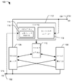
도 1를 참조하면, 레벨 시프팅 회로 장치의 제 1의 예시적인 실시예가 도시되며 일반적으로 도면부호 100으로 표시된다. 레벨 시프팅 회로 장치(100)는 입력 전압 신호를 수신하기 위한 입력(102)을 포함한다. 출력(104)은 레벨 시프트된 전압 신호를 제공한다. 제 1 약한 상태 홀딩 경로(106)는 입력(102) 및 출력(104)에 연결된다. 제 1 약한 상태 홀딩 경로(106)는 입력(102)에 연결되는 제 2 약한 상태 홀딩 경로(108)에 교차-연결(cross-couple)된다. 전압 풀-업 로직 회로(110)는 제 1 약한 상태 홀딩 경로(106) 및 제 2 약한 상태 홀딩 경로(108) 모두에 연결된다. 제어 경로(112)는 전압 풀-업 로직 회로(110)에 제어 신호를 제공하도록 연결된다.Referring to FIG. 1, a first exemplary embodiment of a level shifting circuit arrangement is shown and generally indicated by the
특정 실시예에서, 입력(102)에 수신된 입력 전압 신호는 높은 상태(V1L) 및 낮은 상태(V0)사이의 제 1 전압 범위내에 있다. 입력 전압 신호에 응답하여, 제 1 약한 상태 홀딩 회로(106)는 높은 상태(V1H) 및 낮은 상태(V0) 사이의 제 2 전압 범위내에 있는 레벨 시프트된 전압 신호를 출력(104)에서 발생시킨다. 특정 실시예에서, 제 1 약한 상태 홀딩 경로(106) 및 제 2 약한 상태 홀딩 경로(108)는 0.6-1.4 V 또는 이 0.6-1.4 V 보다 낮은 전압의 레벨 시프팅을 포함하는, 입력 전압들의 큰 범위의 레벨 시프팅을 인에이블(enable)하도록 구성된다. 그러나, 입력 전압들의 큰 범위에 걸쳐 동작할 수 있는 결과로서, 제 1 약한 상태 홀딩 경로(106) 및 제 2 약한 상태 홀딩 경로(108)는 입력(102)에서 수신된 입력 신호의 전이에 응답하여 비교적 느린 전이 시간들을 보일 수 있다. In a particular embodiment, the input voltage signal received at
특정 실시예에서, 전압 풀-업 로직 회로(110)는 제 1 약한 상태 홀딩 경로(106) 및 제 2 약한 상태 홀딩 경로(108)에 전류를 제공함으로써 출력(104)에서의 스위칭 속도를 개선하도록 동작한다. 전압 풀-업 로직 회로(110)에 의하여 약한 상태 홀딩 경로들(106, 108)에 제공되는 추가 전류는 입력 신호의 전이에 대한 고속 응답을 인에이블한다. 특정 실시예에서, 전압 풀-업 로직 회로(110)는 주로 입력(102)에서 수신되는 입력 신호의 검출된 전이에 응답하여 제 1 약한 상태 홀딩 경로(106) 및 제 2 약한 상태 홀딩 경로(108) 중 적어도 하나에 레벨 시프팅 전류를 제공하도록 동작한다. 전압 풀-업 로직 회로(110)는 비-전이(non-transition) 기간들 동안 입력(102)의 저전압 신호들로 약한 상태 홀딩 경로들(106, 108)의 감도(sensitivity)를 유지하기 위하여 제어 경로(112)에 응답하여 약한 상태 홀딩 경로들(106, 108)에 전류를 제공하는 것을 중지시킨다. In a particular embodiment, the voltage pull-
제어 경로(112)는 전압 풀-업 로직 회로(110)의 활성화(activation)를 선택적으로 제어하기에 적합하다. 특정 실시예에서, 제어 경로(112)는 출력(104)으로부터 전압 풀-업 로직 회로(110)로의 자체-타이밍된(self-timed) 피드백 경로(118)를 포함한다. 제어 경로(112)는 출력(104)에서의 전압 레벨 변화를 검출하도록 동작할 수 있으며, 출력(104)에서의 전이에 기초하여 특정 지연이 경과한 것을 자체-타이밍된 피드백 경로(118)가 결정할때 약한 상태 홀딩 경로들(106, 108) 중 하나 이상의 경로로의 전류를 턴-오프(turn off) 시키기 위하여 전압 풀-업 제어 로직(110)에 활성화 신호를 제공하도록 동작할 수 있다. The
다른 실시예에서, 제어 경로(112)는 입력(102)에 연결되는 지연 로직 회로(114)를 포함한다. 이러한 실시예에서, 제어 경로(112)는 입력(102)에서의 전이를 검출하고 전압 풀-업 로직 회로(110)에 활성화 신호를 전송하도록 동작한다. 활성화 신호는 약한 상태 홀딩 경로 (106), 약한 상태 홀딩 경로(108) 또는 이들 모두가 로직 상태들사이에서 전이하는 것을 돕기 위하여 전압 풀-업 로직 회로(110)가 전류를 소싱(sourcing)하는 것을 시작하도록 할 수 있다. 제어 경로(112)는 입력(102)의 전이 이후로부터 충분한 지연이 경과하였다는 것을 결정한 지연 로직 회로(114)에 응답하여 전압 풀-업 로직 회로(110)에 제 2 제어 신호를 전송하도록 추가로 동작할 수 있다. 제 2 제어 신호는 전압 풀-업 로직 회로(110)를 비활성화할 수 있어서, 입력 전압들의 넓은 범위에 걸쳐 약한 상태 홀딩 경로들(106, 108)의 정상 동작을 다시 시작하게 할 수 있다. 특정 실시예에서, 지연 로직 회로(114)는 조절가능하며, 제 2 제어 신호와 연관된 지연을 제어하기 위하여 조절가능 지연 컴포넌트(116)를 포함할 수 있다. In another embodiment, the
동작 동안, 제 1 입력 신호는 제 1 전자 컴포넌트로부터 입력(102)에서 수신될 수 있다. 레벨 시프팅 회로 장치(110)는 입력 전압 레벨을 전환하거나 또는 시프트할 수 있으며, 출력(104)에서 출력 전압 레벨을 발생시킬 수 있다. 예컨대, 입력 신호는 프로세서, 버스, 메모리, 또는 다른 전자 컴포넌트들로부터 수신될 수 있으며, 출력은 프로세서, 버스, 메모리, 또는 다른 전자 컴포넌트들에 제공될 수 있다. 제 1 입력 신호는 제 1 전원과 연관된 전압 레벨들 VO 내지 V1L을 반영할 수 있다. 출력(104)은 제 2 전압 레벨들 V0 내지 V1H에서 동작하는 하나 이상의 다른 전자 컴포넌트들에 연결될 수 있다. 예시적인 예로서, 제 1 전압 레벨은 0V 내지 1.0V의 전압 범위와 연관된 신호일 수 있으며, 제 2 전압 레벨은 0V 내지 3.3V의 전압 범위와 연관된 신호일 수 있다. During operation, a first input signal may be received at
제 2 입력 신호에 대한, 입력(102)의 전이에 응답하여, 제 1 및 제 2 약한 상태 홀딩 경로들(106, 108)은 상태들사이에서 전이를 시작한다. 전압 풀-업 로직 회로(110)는 하나 이상의 트랜지스터들에 전하(charge)를 공급함으로써 전압 레벨 전이를 돕기 위하여 제 1 약한 상태 홀딩 경로(106), 제 2 약한 상태 홀딩 경로(108) 또는 이들 모두에 전류를 공급하는 것을 시작한다. 특정 실시예에서, 전압 풀-업 로직 회로(110)는 약한 상태 홀딩 경로들(106, 108) 중 적어도 하나가 상태들 사이에서 전이를 시작하였다는 것을 검출하는 것에 응답하여 전류를 공급하는 것을 시작한다. 다른 실시예에서, 전압 풀-업 로직 회로(110)는 대신에 제어 경로(112)로부터의 제어 신호에 응답하여 전류를 공급하는 것을 시작할 수 있다.In response to the transition of the
예컨대 자체-타이밍된 피드백 경로(118) 또는 지연 로직 회로 경로(114)를 통한 적절한 지연기간 후에, 제어 경로(112)는 약한 상태 홀딩 경로들(106, 108)에 전류를 소싱하는 것을 중지시키기 위하여 전압 풀-업 로직 회로(110)를 비활성화시키는 제어 신호를 제공한다. 전압 풀-업 로직 회로(110)의 비활성화 후에, 교차-연결된 약한 상태 홀딩 경로들(106, 108)은 출력(104)에서 새로운 출력 전압 레벨을 유지한다. 전압 풀-업 로직 회로(110)를 선택적으로 활성화시킴으로써, 입력 동작 전압들의 넓은 범위 및 고속 출력 레벨 전이 모두가 레벨 시프팅 회로 장치(100)에 의하여 제공된다.For example, after a suitable delay period through self-timed
도 2를 참조하면, 레벨 시프팅 회로 장치의 제 2의 예시적인 실시예가 도시되며 일반적으로 도면부호 200으로 표시된다. 레벨 시프팅 회로 장치(200)는 고전압 VddL 및 저전압 Vss 사이의 제 1 전압 범위에 대응하는 입력 신호를 수신하도록 구성된 입력(202)을 포함한다. 레벨 시프팅 회로 장치(200)는 또한 제 2 전압 범위까지 입력(202)의 레벨 시프팅에 대응하는 출력 신호를 제공하도록 구성된 출력(204)을 포함하며, 여기서 높은 신호는 고전압 VddH에 의하여 표현되고 낮은 신호는 저전압 Vss에 의하여 표현된다. 레벨 시프팅 회로 장치(200)는 또한 제 1 약한 상태 홀딩 경로(206) 및 제 2 약한 상태 홀딩 경로(208)를 포함한다. 제 1 약한 상태 홀딩 경로(206)는 입력(202)에 연결되며, 제 2 약한 상태 홀딩 경로(208)는 제 1 전압 범위에서 동작하는 인버터(207)를 통해 입력(202)에 연결된다. 전압 풀-업 로직 회로(210)는 제 1 약한 상태 홀딩 경로(206) 및 제 2 약한 상태 홀딩 경로(208) 모두에 연결된다. 제어 경로(212)는 전압 풀-업 로직 회로(210) 및 출력(204)에 연결된다.With reference to FIG. 2, a second exemplary embodiment of a level shifting circuit arrangement is shown and generally indicated by the numeral 200. Level shifting
특정 실시예에서, 제 1 약한 상태 홀딩 경로(206)는 전원 전압 VddH에 연결되는 제 1 단자, 제 2 약한 상태 홀딩 경로(208)에 연결되는 제어 단자 및 제 3 단자를 가진 제 1 약한 p-채널 트랜지스터(220)를 포함한다. 제 1 약한 상태 홀딩 경로(206)는 또한 제 1 약한 p-채널 트랜지스터(220)의 제 3 단자에 연결되는 제 4 단자를 포함하는 제 2 약한 p-채널 트랜지스터(222)를 포함한다. 제 2 약한 p-채널 트랜지스터(222)는 입력(202)에 연결되는 제 2 제어 단자 및 제 1 노드(223)에 연결되는 제 5 단자를 가진다. 제 1 노드(223)는 전압 풀-업 로직 회로(210)에 연결된다. 제 1 약한 상태 홀딩 경로(206)는 또한 제 1 노드(223)에 연결되는 제 6 단자, 입력(202)에 연결되는 제 3 제어 단자, 및 제 2 전원 전압 Vss에 연결되는 제 7 단자를 포함하는 강한(strong) n-채널 트랜지스터(224)를 가진다. 여기에서 사용된 바와같이, 강한 트랜지스터는 약한(weak) 트랜지스터보다 게이트 전압과 같은, 제어 단자의 신호에 대한 고속 전류 응답을 가지며, 약한 트랜지스터보다 더 넓고 더 짧은 채널을 가질 수 있다. 예컨대, 약한 p-채널 트랜지스터들(220, 222)은 대략 0.12 마이크로미터(um) 넓이 및 0.1um 길이를 가진 채널들을 가진 p-채널 MOSFET들일 수 있으며, 강한 n-채널 트랜지스터(224)는 대략 0.6 um 넓이 및 0.04 um 길이를 가진 채널을 가진 n-채널 MOSFET일 수 있다. In a particular embodiment, the first weak
특정 실시예에서, 제 2 약한 상태 홀딩 경로(208)는 전원 전압 VddH에 연결되는 제 1 단자, 제 1 약한 상태 홀딩 경로(206)에 연결되는 제어 단자, 및 제 2 약한 p-채널 트랜지스터(232)에 연결되는 제 3 단자를 포함하는 제 1 약한 p-채널 트랜지스터(230)를 포함한다. 제 2 약한 p-채널 트랜지스터(232)는 제 1 약한 p-채널 트랜지스터(230)의 제 3 단자에 연결되는 제 4 단자, 인버터(207)의 출력에 연결되는 제 2 제어 단자, 및 제 2 노드(233)에 연결되는 제 5 단자를 포함한다. 강한 n-채널 트랜지스터(234)는 제 2 노드(233)에 연결되는 제 6 단자, 인버터(207)의 출력에 연결되는 제 3 제어 단자, 및 제 2 전원 전압 Vss에 연결되는 제 7 단자를 가진다. 제 2 약한 상태 홀딩 경로(208)의 제 2 노드(233)는 제 1 약한 상태 홀딩 경로(206)의 제 1 약한 p-채널 트랜지스터(220)의 제 1 제어 단자에 연결된다. 마찬가지로, 제 1 약한 상태 홀딩 경로(206)의 제 1 노드(223)는 제 2 약한 상태 홀딩 경로(208)의 제 1 약한 p-채널 트랜지스터(230)의 제 1 제어 단자에 연결된다. In a particular embodiment, the second weak
풀-업 로직 회로(210)는 제 2 약한 상태 홀딩 경로(208)에 연결되는 제 1 강한 풀-업 경로(241)를 포함하며, 또한 제 1 약한 상태 홀딩 경로(206)에 연결되는 제 2 강한 풀-업 경로(246)를 포함한다. 제 1 강한 풀-업 경로(241)는 전원 전압 VddH에 연결되며 제어 경로(212)에 연결되는 제어 단자를 가진 제 1 강한 p-채널 트랜지스터(242)를 포함한다. 제 1 강한 풀-업 경로(241)는 제 1 강한 p-채널 트랜지스터(242)에 연결되고 추가로 제 1 노드(223)에 연결되는 제 2 강한 p-채널 트랜지스터(244)를 가진다. 제 2 강한 p-채널 트랜지스터(244)는 제 2 노드(233)에 연결되는 제어 단자를 가진다.The pull-up
유사하게, 제 2 강한 풀-업 경로(246)는 전원 전압 VddH에 연결되고 제어 경로(212)에 연결되는 제어 단자를 가진 제 1 강한 p-채널 트랜지스터(248)를 가진다. 제 2 강한 풀-업 경로(246)는 또한 제 1 강한 p-채널 트랜지스터(248) 및 제 2 노드(233)사이에 연결되고 제 1 노드(223)에 연결되는 제어 단자를 가진 제 2 강한 p-채널 트랜지스터(250)를 포함한다.Similarly, the second strong pull-up
출력(204)은 출력 인버터(266)를 통해 제 1 노드(223)에 연결된다. 제어 경로(212)는 출력(204)에, 제 2 강한 풀-업 경로(246)의 제 1 강한 p-채널 트랜지스터(248)의 제어 단자에, 그리고 인버터(270)를 통해 제 1 강한 풀-업 경로(241)의 제 1 강한 p-채널 트랜지스터(242)의 제어 단자에 연결된다. 제어 경로(212)는 출력(204)으로부터 전압 풀-업 로직 회로(210)로의 자체-타이밍된 피드백 경로를 포함한다. 특히, 전압 풀-업 로직 회로(210)는 노드들(223 또는 233) 중 하나가 저전압 레벨로부터 고전압 레벨로 전이할때 동작하는 것을 시작하며, 제 1 노드(223)에서의 전압 전이가 출력 인버터(266)를 통해 강한 풀-업 경로들(241, 246)의 트랜지스터들(242, 248)의 제어 단자들에 전파할때까지 동작하는 것을 계속한다. 제어 경로(212)에 의하여 강한 풀-업 경로들(241, 246)의 트랜지스터들(242, 248)에 제공되는 결과적인 제어 신호는 전압 풀-업 로직 회로(210)를 비활성화시킨다.The
정상-상태(steady-state) 동작 동안, 전압 풀-업 로직 회로(210)는 오프(off)된다. 특히, 제 1 강한 전류 경로(241)의 트랜지스터들(242, 244) 중 적어도 하나는 오프(off)되며(즉, 비-전도되며), 제 2 강한 전류 경로(246)의 트랜지스터들(248, 250) 중 적어도 하나는 오프(off)된다.During steady-state operation, the voltage pull-up
낮은 신호(예컨대, Vss)가 입력(202)에서 유지될때, 제 1 약한 상태 홀딩 경로(206)의 강한 n-채널 트랜지스터(224)는 오프(off)되고 2개의 약한 p-채널 트랜지스터들(220, 222)은 온(on)되어, 고전압(예컨대, "1" 신호로서 인식될 전압들을 포함하는 것으로 여기에서 사용되는 VddH)으로 제 1노드(223)를 바이어싱한다. 출력 인버터(266)는 제 1 노드(223)에 연결되는 입력을 가지며, 저전압(예컨대, "0" 신호로서 인식되는 전압들을 포함하는 것으로 여기에서 사용되는 Vss)을 출력한다. 제 2 약한 상태 홀딩 경로(208)의 강한 n-채널 트랜지스터(234)는 온(on)되고 약한 p-채널 트랜지스터들(230, 232)은 오프(off)되어 제 2 노드(233)를 저전압으로 바이어싱한다. 전압 풀-업 로직 회로(210)에서, 제 1 강한 풀-업 경로(241)의 제 1 트랜지스터(242)는 오프(off)되고 제 2 트랜지스터(244)는 온(on)된다. 역으로, 제 2 강한 풀-업 경로(246)의 제 1 트랜지스터(248)는 온(on)되고 제 2 트랜지스터(250)는 오프(off)된다.When a low signal (eg, Vss) is maintained at the
입력(202)이 낮은 신호로부터 높은 신호로(예컨대, Vss로부터 VddL로) 전이될때, 제 1 약한 상태 홀딩 경로(206)의 강한 n-채널 트랜지스터(224)가 턴-온(turn-on)되어, 제 1 노드(223)가 고전압 상태(예컨대, VddH)로부터 저전압 상태(예컨대, Vss)로 되게 한다. 전이동안, 약한 p-채널 트랜지스터들(220, 222)은 VddH 및 VddL에 의하여 결정된 상태들에서 동작한다. 비록 약한 p-채널 트랜지스터(222)가 온(on)될 수 있을지라도, n-채널 트랜지스터(234)가 제 1 노드를 고전압 상태로 바이어싱하도록 조정하면, 더 강한 n-채널 트랜지스터(224)는 제 1 노드를 저전압 상태로 풀(pull)한다. 유사하게, 제 2 약한 상태 홀딩 경로(208)의 강한 n-채널 트랜지스터(234)가 턴-오프되어, 제 2 노드(233)가 저전압으로부터 고전압으로 되게 하나, 전이는 약한 p-채널 트랜지스터(232)를 통해 흐르는 전류에 의하여 제한된다.When the
그러나, 제 1 노드(223)가 낮은 상태로 전이될때, 제 2강한 풀-업 경로(246)의 강한 p-채널 트랜지스터(250)는 턴-온되는 반면에 트랜지스터(248)는 또한 온(on)을 유지한다. 따라서, 전류는 강한 n-채널 트랜지스터(234)를 충전하기 위하여 제 2 강한 풀-업 전류 경로(246)를 통해 흐른다. 제 1 노드(223)가 낮은 상태로 전이될때, 출력 인버터(266)는 낮은 상태로부터 높은 상태로 전이되며, 이는 제어 경로(212)를 통해 트랜지스터(248)의 제어 단자에 제공되어 제 2 강한 풀-업 경로(246)를 턴-오프시킨다. However, when the
높은 신호(예컨대, VddL)가 입력(202)에서 유지될때, 제 1 약한 상태 홀딩 경로(206)의 강한 n-채널 트랜지스터(224)가 온(on)되고 약한 p-채널 트랜지스터들(220, 222)이 오프(off)되어 제 1 노드(223)를 저전압(예컨대, VddL)으로 바이어싱한다. 출력 인버터(266)는 고전압(예컨대, VddH)을 출력한다. 제 2 약한 상태 홀딩 경로(208)의 강한 n-채널 트랜지스터(234)는 오프(off)되어, 제 2 노드(233)를 고전압으로 바이어싱한다. 전압 풀-업 로직 회로(210)에서, 제 1 강한 풀-업 경로(241)의 제 1 트랜지스터(242)는 온(on)되며 제 2 트랜지스터(244)는 오프(off)된다. 역으로, 제 2 강한 풀-업 경로(246)의 제 1 트랜지스터(248)는 오프(off)되며 제 2 트랜지스터(250)는 온(on)된다.When a high signal (eg, VddL) is maintained at the
입력(202)이 높은 신호로부터 낮은 신호로(예컨대, VddL로부터 Vss로) 전이될때, 인버터(207)의 출력은 낮은 상태로부터 높은 상태로 전이되어 제 2 약한 상태 홀딩 경로(208)의 강한 n-채널 트랜지스터(234)를 턴-온시키며 제 2 노드(233)가 고전압 상태로부터 저전압 상태로 되게 한다. 전이 동안, 약한 p-채널 트랜지스터들(230, 232)은 VddH 및 VddL에 의하여 결정된 상태들에서 동작한다. 비록 약한 p-채널 트랜지스터(232)가 온(on)될 수 있을지라도, n-채널 트랜지스터(234)가 고전압 상태로 제 2 노드를 바이어싱하도록 조정하면, 더 강한 n-채널 트랜지스터(234)가 제 2 노드를 저전압 상태로 풀(pull)한다.When the
제 2 노드(233)가 저전압 상태로 전이될때, 제 1 강한 풀-업 경로(241)의 강한 p-채널 트랜지스터(244)는 턴-온되는데 반해 트랜지스터(242)는 온(on)을 유지한다. 더욱이, 약한 p-채널 트랜지스터(220)는 또한 턴-온된다. 따라서, 전류는 제 1 노드(222)를 충전시키기 위하여 제 1 강한 풀-업 전류 경로(241) 및 제 1 약한 상태 홀딩 경로(206)를 통해 흐르는 반면에, 강한 n-채널 트랜지스터(224)는 턴-오프된다. 제 1 노드(223)가 높은 상태로 전이될때, 출력 인버터(266)는 높은 상태로부터 낮은 상태로 전이되며, 이는 제어 경로(212) 및 인버터(270)를 통해 트랜지스터(242)의 제어 단자에 제공되어 제 1 강한 풀-업 경로(241)를 턴-오프시킨다. When the
따라서, 입력(202)의 전이동안, 높은 상태로부터 낮은 상태로의 노드들(223, 233) 중 하나의 노드의 초기 전이는 각각의 약한 p-채널 트랜지스터들(220-222 또는 230-232)에 의하여 제한되나, 낮은 상태로부터 높은 상태로의 다른 노드(223 또는 233)의 전이는 전압 풀-업 제어 회로(210)에 의하여 도움을 받는다. 입력(202)이 높은 또는 낮은 신호에서 유지될때, 전압 풀-업 제어 회로(210)는 오프(off)되며, 교차-연결된 약한 상태 홀딩 경로들(206, 208)은 입력(202)에서 저전압 입력 범위들까지 감도(sensitive)를 유지한다. 입력(202)에서 전이가 발생할때, 전압 풀-업 로직 회로(210)는 새로운 상태로의 전이를 가속시키기 위하여 약한 상태 홀딩 경로들(206, 208)에 전류를 공급하도록 활성화된다. 전압 풀-업 로직 회로(210)는 제어 경로(212)에 응답하여 비활성화되어 출력(204)에서의 전이를 표시한다. 따라서, 전압 풀-업 로직 회로(210)는 입력(202)에 응답하여 상태들간의 약한 상태 홀딩 경로들(206, 208) 전이를 돕기 위하여 전류의 펄스를 제공한다. 전압 풀-업 회로(210)를 선택적으로 활성화시킴으로써, 입력 동작 전압들의 넓은 범위 및 고속 출력 레벨 전이 모두가 레벨 시프팅 회로 장치(200)에 의하여 제공된다.Thus, during the transition of
도 3은 레벨 시프팅 회로 장치를 포함하는 시스템(300)의 특정 예시적인 실시예에 대한 블록도이다. 구조(302)는 메모리 셀 선택 신호를 수신하도록 연결된 제 1 입력(304)을 포함한다. 제 2 입력(306)은 데이터 신호를 수신하도록 연결된다. 제 1 입력(304)은 제 1 레벨 시프팅 회로(308)에 제공되며, 제 2 입력(306)은 제 2 레벨 시프팅 회로(310)에 제공된다. 메모리 어레이(312)는 제 1 레벨 시프팅 회로(308) 및 제 2 레벨 시프팅 회로(310)가 출력을 수신하도록 연결된다. 구조(302)는 제 1 전압 레벨 Vstruct에서 동작하며, 메모리 어레이(312)는 제 2 전압 레벨 Varray에서 동작한다.3 is a block diagram of a particular illustrative embodiment of a
제 1 레벨 시프팅 회로(308)는 제 1 입력(304)을 수신하기 위한 입력(320) 및 메모리 어레이(312)에 제 1 레벨 시프트된 전압 신호를 제공하기 위한 출력(321)을 포함한다. 제 1 레벨 시프팅 회로(308)는 입력(320) 및 출력(321)에 연결되는 제 1 약한 상태 홀딩 경로(322)를 포함한다. 제 1 약한 상태 홀딩 경로(322)는 또한 제 2 약한 상태 홀딩 경로(326)와 같은 교차-연결 회로(cross-coupling circuit)에 연결된다. 전압 풀-업 로직 회로(328)는 제 1 약한 상태 홀딩 경로(322) 및 제 2 약한 상태 홀딩 경로(326)에 연결된다. 제어 경로(324)는 전압 풀-업 로직 회로(328)의 활성화를 선택적으로 제어하기 위하여 전압 풀-업 로직 회로(328)에 연결된다. 특정 실시예에서, 제 1 레벨 시프팅 회로(308)는 도 1-2에 도시된 레벨 시프팅 회로 장치(100 또는 200)를 포함할 수 있다.The first
제 2 레벨 시프팅 회로(310)는 제 1 입력(306)을 수신하기 위한 입력(330) 및 메모리 어레이(312)에 제 1 레벨 시프트된 전압 신호를 제공하기 위한 출력(331)을 포함한다. 특정 실시예에서, 제 2 레벨 시프팅 회로(310)는 입력(330) 및 출력(331)에 연결되는 제 1 약한 상태 홀딩 경로(332)를 포함한다. 제 1 약한 상태 홀딩 경로(332)는 또한 제 2 약한 상태 홀딩 경로(336)와 같이 교차-연결 회로에 연결된다. 전압 풀-업 로직 회로(338)는 제 1 약한 상태 홀딩 경로(332) 및 제 2 약한 상태 홀딩 경로(336)에 연결된다. 제어 경로(334)는 전압 풀-업 로직 회로(338)의 활성화를 선택적으로 제어하기 위하여 전압 풀-업 로직 회로(338)에 연결된다. 특정 실시예에서, 제 2 레벨 시프팅 회로(310)는 도 1-2에 도시된 레벨 시프팅 회로 장치(100 또는 200)를 포함할 수 있다.The second
동작동안, 제 1 입력(304) 및 제 2 입력(306) 중 적어도 하나는 Vstruct와 같은 제 1 전압 레벨에 있을 수 있으나, 메모리 어레이(312)는 Varray와 같은 제 2 전압 레벨로 전원에 의하여 전력이 공급될 수 있다. 예컨대, 제 1 전압 레벨은 제 2 전압 레벨보다 낮을 수 있다. 레벨 시프팅 회로들(306, 308)은 메모리 어레이(312)에 적합한 전압 레벨들까지 입력들(304, 306)의 전압 레벨들을 시프트할 수 있다. 특정 실시예에서, 레벨 시프팅 회로들(306, 308)은 각각 제어 경로들(324, 334)에 의하여 선택적으로 활성화되는 풀-업 로직 회로들(328, 338)을 포함하며, 따라서 입력 신호들의 변화들에 응답하여 고속 전이들을 인에이블하고 또한 넓은 범위의 동작을 인에이블한다. 예컨대, 레벨 시프팅 회로들(306, 308)은 0.6-1.4 V를 포함하는 전압 범위에서 동작가능할 수 있다.During operation, at least one of the
도 4는 도 1-3에 기술된 회로 장치들과 같은 회로 장치를 사용하는 레벨 시프팅 방법에 대한 특정한 예시적인 실시예에 대한 흐름도이다. 단계(402)에서, 입력 전압은 전압 풀-업 로직을 포함하는 레벨 시프팅 회로에 대한 입력에서 수신된다. 특정 실시예에서, 입력 신호는 제 1 약한 상태 홀딩 경로에 공급된다. 제 1 약한 상태 홀딩 경로는 직렬로 배열된, 다수의 약한 p-채널 트랜지스터들 및 강한 n-채널 트랜지스터를 포함할 수 있다. 4 is a flowchart of a particular illustrative embodiment of a level shifting method using a circuit device such as the circuit devices described in FIGS. 1-3. In
단계(404)로 이동하면, 출력 신호는 레벨 시프팅 회로로부터 제공된다. 특정 실시예에서, 입력 신호는 제 1 전압을 가지고 출력 신호는 제 2 전압을 가진다. 단계(406)로 전진하면, 레벨 시프팅 회로의 전압 풀-업 로직 회로는 선택적으로 활성화된다. 특정 실시예에서, 전압 풀-업 로직 회로는 약한 상태 홀딩 경로의 전이 시간을 감소시키기 위하여 전하(charge)를 제공한다.Moving to step 404, the output signal is provided from a level shifting circuit. In a particular embodiment, the input signal has a first voltage and the output signal has a second voltage. Moving forward to step 406, the voltage pull-up logic circuit of the level shifting circuitry is selectively activated. In a particular embodiment, the voltage pull-up logic circuit provides a charge to reduce the transition time of the weak state holding path.
단계(408)로 계속되면, 특정 실시예에서, 제어 신호는 전압 풀-업 로직 회로에 제공된다. 제어 신호는 출력 신호에 응답하는 피드백 신호일 수 있다. 특정 실시예에서, 제어 신호는 전압 풀-업 로직 회로가 약한 상태 홀딩 경로를 충전시키는 것을 중지하도록 한다. 특정 실시예에서, 전압 풀-업 로직 회로의 출력은 입력 신호에 응답하여 시작하며 제어 신호에 응답하여 종료하는 전류 펄스를 포함한다. Continuing with
도 5는 도 1-4에 기술된 회로들 및 방법들의 실시예들이 사용될 수 있는 대표적인 이동 통신 장치(500)의 블록도이다. 통신 장치(500)는 디지털 신호 프로세서(DSP)(510)와 같은 프로세서를 포함한다. 전압 풀-업 로직(564)을 가진 레벨 시프팅 회로는 DSP(510) 및 메모리 장치(532)간의 전압 레벨 시프트를 제공하기 위하여 DSP(510)에 연결된다. 예시적인 실시예에서, 전압 풀-업 로직(564)을 가진 레벨 시프팅 회로는 도 1-3에 예시된 회로 장치(100, 200, 308, 또는 310)를 포함한다. 예시적인 실시예에서, 전압 풀-업 로직(564)을 가진 레벨 시프팅 회로는 도 4에 예시된 방법을 수행한다.5 is a block diagram of an exemplary
도 5는 또한 디지털 신호 프로세서(510) 및 디스플레이(528)에 연결되는 디스플레이 제어기(526)를 도시한다. 코더/디코더(CODEC)(534)는 또한 디지털 신호 프로세서(510)에 연결될 수 있다. 스피커(536) 및 마이크로폰(538)은 CODEC(534)에 연결될 수 있다.5 also shows a
도 5는 무선 제어기(540)가 디지털 신호 프로세서(510) 및 무선 안테나(542)에 연결될 수 있다는 것을 예시한다. 특정 실시예에서, 입력 장치(530) 및 전원(544)은 온-칩 시스템(522)에 연결된다. 더욱이, 특정 실시예에서, 도 5에 예시된 바와같이, 디스플레이(528), 입력 장치(530), 스피커(536), 마이크로폰(538), 무선 안테나(542), 및 전원(544)은 온-칩 시스템(522) 외부에 있다. 그러나, 각각은 인터페이스 또는 제어기와 같은 온-칩 시스템(522)의 컴포넌트에 연결될 수 있다. 5 illustrates that the
비록 전압 풀-업 로직(564)을 가진 레벨 시프팅 회로가 DSP(510) 및 메모리 장치(532)간에 레벨 시프트를 제공하기 위하여 연결되는 것으로 도시될지라도, 전압 풀-업 로직(564)을 가진 레벨 시프팅 회로는 또한 상이한 전압 레벨들을 사용하는 통신 장치(500)의 다른 컴포넌트들간에 레벨 시프팅을 제공하기 위하여 사용될 수 있다. 예컨대, 전압 풀-업 로직(564)을 가진 레벨 시프팅 회로는 온-칩 시스템(522), 디스플레이(528), 입력 장치(530), 스피커(536), 마이크로폰(538), 무선 안테나(542), 전원(544) 또는 이들의 임의의 조합사이에 연결될 수 있다. 다른 예로서, 전압 풀-업 로직(564)을 가진 레벨 시프팅 회로는 DSP(510) 및 온-칩 시스템(522)의 임의의 다른 컴포넌트사이에 연결될 수 있다. 또 다른 예로서, 전압 풀-업 로직(564)을 가진 레벨 시프팅 회로는 예컨대 DSP(510)내에서 보다 낮은 전압 레벨로 동작하는 레지스터 파일에서 DSP(510)의 컴포넌트들에 대한 레벨 시프팅을 제공하기 위하여 DSP(510)와 집적될 수 있다. Although the level shifting circuit with the voltage pull-up
개시된 시스템들 및 방법들과 관련하여, 전압 레벨 시프팅은 예컨대 도 1-3에 예시된 입력들(102, 202, 320, 330)과 같이 전압 풀-업 로직을 포함하는 레벨 시프팅 회로에 대한 입력에서 입력 전압을 수신하기 위한 수단을 포함하는 장치에 의하여 수행될 수 있다. 장치는 또한 예컨대 출력들(104, 204, 321, 331) 및 도 1-3에 도시된 각각의 출력들에 연결되는 대응하는 회로 구조들과 같이, 레벨 시프팅 회로로부터 출력 신호를 제공하기 위한 수단을 포함할 수 있다. 장치는 또한 도 1-3에 예시된 제어 경로들(112, 212, 324, 334)과 같이 레벨 시프팅 회로의 전압 풀-업 로직 회로를 선택적으로 활성화시키기 위한 수단을 포함할 수 있다. With respect to the disclosed systems and methods, voltage level shifting may be applied to a level shifting circuit that includes voltage pull-up logic, such as, for example, the
당업자는 여기에서 제시된 실시예들과 관련하여 기술된 다양한 예시적인 논리 블록들, 구성들, 모듈들, 회로들, 및 알고리즘 단계들이 전자 하드웨어, 컴퓨터 소프트웨어, 또는 이들의 조합으로서 구현될 수 있음을 추가로 인식할 것이다. 하드웨어 및 소프트웨어의 상호 호환성을 명확히 예시하기 위해, 다양한 예시적인 컴포넌트들, 블록들, 구성들, 모듈들, 회로들, 및 단계들이 일반적으로 그들의 기능적 관점에서 앞서 기술되었다. 이러한 기능이 하드웨어로 구현되는지, 또는 소프트웨어로 구현되는지는 특정 애플리케이션 및 전체 시스템에 대해 부가된 설계 제한들에 의존한다. 당업자는 기술된 기능들을 각각의 특정 애플리케이션에 대해 다양한 방식으로 구현할 수 있지만, 이러한 구현 결정들이 본 발명의 범위로부터 벗어나는 것으로 해석되지 않아야 한다.Those skilled in the art will further appreciate that the various illustrative logical blocks, configurations, modules, circuits, and algorithm steps described in connection with the embodiments presented herein may be implemented as electronic hardware, computer software, or a combination thereof. Will be recognized. To clearly illustrate the interchangeability of hardware and software, various illustrative components, blocks, configurations, modules, circuits, and steps have been described above generally in terms of their functionality. Whether such functionality is implemented as hardware or software depends upon the particular application and design constraints imposed on the overall system. Skilled artisans may implement the described functionality in varying ways for each particular application, but such implementation decisions should not be interpreted as causing a departure from the scope of the present invention.
여기에서 제시된 실시예들과 관련하여 기술된 알고리즘 또는 방법의 단계들은 하드웨어, 프로세서에 의해 실행되는 소프트웨어 모듈, 또는 이들의 조합에 의해 직접 구현될 수 있다. 소프트웨어 모듈들은 RAM 메모리; 플래시 메모리; ROM 메모리; PROM 메모리; EPROM 메모리; EEPROM 메모리; 레지스터들; 하드디스크; 휴대용 디스크; CD-ROM; 또는 공지된 임의의 다른 형태의 저장 매체에 상주할 수 있다. 예시적인 저장매체는 프로세서와 연결되어, 프로세서는 저장매체로부터 정보를 판독하고 저장매체에 정보를 기록할 수 있다. 대안적으로, 저장 매체는 프로세서의 구성요소일 수 있다. 프로세서 및 저장매체는 ASIC 에 위치할 수 있다. ASIC 는 컴퓨팅 장치 또는 사용자 단말에 위치할 수 있다. 대안적으로, 프로세서 및 저장 매체는 컴퓨팅 장치 또는 사용자 단말에서 개별 컴포넌트들로서 존재할 수 있다. The steps of an algorithm or method described in connection with the embodiments presented herein may be implemented directly by hardware, a software module executed by a processor, or a combination thereof. Software modules include a RAM memory; Flash memory; ROM memory; PROM memory; EPROM memory; EEPROM memory; Registers; Hard disk; Portable disk; CD-ROM; Or may reside in any other form of storage medium known in the art. An exemplary storage medium is coupled to the processor such that the processor can read information from, and write information to, the storage medium. In the alternative, the storage medium may be integral to the processor. The processor and the storage medium may be located in an ASIC. The ASIC may be located in a computing device or a user terminal. In the alternative, the processor and the storage medium may reside as discrete components in a computing device or user terminal.
제시된 실시예들에 대한 이전 설명은 당업자가 제시된 실시예들을 이용하거나 또는 실시할 수 있도록 제공된다. 이러한 실시예들에 대한 다양한 수정들은 당업자에게 명백할 것이며, 여기에서 정의된 일반적인 원리들은 본 발명의 사상 또는 범위를 벗어남이 없이 다른 실시예들에 적용될 수 있다. 그리하여, 본 발명은 여기에 제시된 실시예들로 한정되는 것이 아니라, 이하의 청구범위에 의하여 한정된 원리들 및 신규한 특징들과 일관되는 최광의의 범위에서 해석되어야 할 것이다.
The previous description of the presented embodiments is provided to enable any person skilled in the art to make or use the disclosed embodiments. Various modifications to these embodiments will be apparent to those skilled in the art, and the generic principles defined herein may be applied to other embodiments without departing from the spirit or scope of the invention. Thus, the present invention should not be limited to the embodiments set forth herein but should be construed in the broadest scope consistent with the principles and novel features defined by the following claims.
Claims (25)
입력 전압 신호를 수신하기 위한 단일 입력부 및 상기 입력 전압 신호에 대해 인버팅되는 레벨 시프트된 전압 신호를 제공하기 위한 인버팅 출력부를 포함하는 전압 레벨 시프터
를 포함하고,
상기 전압 레벨 시프터는 추가로:
상기 단일 입력부에 연결되는 제1 약한(weak) 상태 홀딩 경로 ? 상기 제1 약한 상태 홀딩 경로는 제1 p-채널 전계 효과 트랜지스터(PFET)와 직렬로 연결되는 제1 n-채널 전계 효과 트랜지스터(NFET)를 포함함 ?;
상기 인버팅 출력부에 연결되는 제2 약한 상태 홀딩 경로 ? 상기 제2 약한 상태 홀딩 경로는 제2 PFET에 직렬로 연결되는 제2 NFET를 포함함 ?;
상기 입력 전압 신호에 응답하는 제1 인버터 ? 상기 제2 NFET 및 상기 제2 PFET는 상기 제1 인버터의 출력에 응답하고, 상기 제1 NFET 및 상기 제1 PFET가 상기 입력 전압 신호에 응답하는 동안에 상기 제1 인버터는 상기 입력 전압 신호의 보수(complement)에 응답하도록 상기 제2 NEFT 및 상기 제2 PFET를 제어함 ?;
상기 제1 약한 상태 홀딩 경로에 그리고 상기 제2 약한 상태 홀딩 경로에 연결되는 전압 풀-업 로직 회로; 및
버퍼의 버퍼 출력의 전이에 응답하여 상기 전압 풀-업 로직 회로의 활성화를 선택적으로 제어하기 위해서 상기 전압 풀-업 로직 회로에 연결되는 제어 경로 ? 상기 버퍼는 상기 인버팅 출력부에 연결되는 입력부를 포함함 ?;
를 포함하고,
상기 버퍼는, 상기 입력 전압 신호의 전이로의 상기 제2 약한 상태 홀딩 경로의 스위칭 응답이 부하에 의해 영향을 받지 않으면서 상기 버퍼 출력부에 인가되는 상기 부하에 응답하도록 상기 전압 풀-업 로직 회로의 제어를 가능하게 하는,
전압을 레벨 시프팅하기 위한 회로 장치.A circuit arrangement for level shifting voltage,
A voltage level shifter comprising a single input for receiving an input voltage signal and an inverting output for providing a level shifted voltage signal inverted with respect to the input voltage signal
Including,
The voltage level shifter further comprises:
A first weak state holding path coupled to the single input; The first weak state holding path comprises a first n-channel field effect transistor (NFET) connected in series with a first p-channel field effect transistor (PFET);
A second weak state holding path coupled to the inverting output; The second weak state holding path comprises a second NFET connected in series with a second PFET;
A first inverter responsive to the input voltage signal; The second NFET and the second PFET are responsive to the output of the first inverter, and while the first NFET and the first PFET are responsive to the input voltage signal, the first inverter is configured to compensate for the input voltage signal. controlling the second NEFT and the second PFET to respond;
A voltage pull-up logic circuit coupled to the first weak state holding path and to the second weak state holding path; And
A control path coupled to the voltage pull-up logic circuit for selectively controlling activation of the voltage pull-up logic circuit in response to a transition of a buffer output of a buffer. The buffer includes an input coupled to the inverting output;
Including,
The buffer may be configured such that the voltage pull-up logic circuit responds to the load applied to the buffer output without the switching response of the second weak state holding path to transition of the input voltage signal being affected by the load. To enable control of
Circuit arrangement for level shifting voltage.
상기 제어 경로는 상기 버퍼 출력부로부터 상기 전압 풀-업 로직 회로로의 자체-타이밍된(self-timed) 피드백 경로를 포함하는,
전압을 레벨 시프팅하기 위한 회로 장치.The method of claim 1,
The control path comprises a self-timed feedback path from the buffer output to the voltage pull-up logic circuit,
Circuit arrangement for level shifting voltage.
상기 제어 경로는 상기 단일 입력부를 상기 전압 풀-업 로직 회로에 연결시키는,
전압을 레벨 시프팅하기 위한 회로 장치.The method of claim 1,
The control path connects the single input to the voltage pull-up logic circuit;
Circuit arrangement for level shifting voltage.
상기 제어 경로는 타이밍 지연을 제공하기 위한 지연 로직 회로를 포함하는,
전압을 레벨 시프팅하기 위한 회로 장치. The method of claim 3,
The control path comprises a delay logic circuit for providing a timing delay,
Circuit arrangement for level shifting voltage.
상기 지연 로직 회로는 조절가능한 지연 컴포넌트를 포함하는,
전압을 레벨 시프팅하기 위한 회로 장치.5. The method of claim 4,
The delay logic circuit comprises an adjustable delay component,
Circuit arrangement for level shifting voltage.
상기 제1 약한 상태 홀딩 경로는,
전원 전압에 연결되는 제1 단자, 상기 제2 약한 상태 홀딩 경로에 연결되는 제어 단자, 및 제3 단자를 포함하는 제3 PFET;
상기 제3 단자에 연결되는 제4 단자, 상기 단일 입력부에 연결되는 제2 제어 단자, 및 노드에 연결되는 제5 단자를 포함하는 상기 제1 PFET ? 상기 노드는 상기 전압 풀-업 로직 회로에 연결됨 ?;
상기 노드에 연결되는 제6 단자, 상기 단일 입력부에 연결되는 제3 제어 단자, 및 제2 전원 전압에 연결되는 제7 단자를 포함하는 상기 제1 NFET
를 포함하는,
전압을 레벨 시프팅하기 위한 회로 장치. The method of claim 1,
The first weak state holding path is
A third PFET comprising a first terminal connected to a power supply voltage, a control terminal connected to the second weak state holding path, and a third terminal;
The first PFET having a fourth terminal connected to the third terminal, a second control terminal connected to the single input unit, and a fifth terminal connected to the node; The node is coupled to the voltage pull-up logic circuit;
The first NFET including a sixth terminal connected to the node, a third control terminal connected to the single input unit, and a seventh terminal connected to a second power supply voltage
/ RTI >
Circuit arrangement for level shifting voltage.
제1 강한 풀-업 경로와 제2 강한 풀-업 경로가 제3 인버터를 통해 연결되는,
전압을 레벨 시프팅하기 위한 회로 장치.The method of claim 1,
A first strong pull-up path and a second strong pull-up path are connected via a third inverter,
Circuit arrangement for level shifting voltage.
상기 제1 약한 상태 홀딩 경로와 상기 제2 약한 상태 홀딩 경로가 상기 제1 인버터를 통해 연결되는,
전압을 레벨 시프팅하기 위한 회로 장치.The method of claim 1,
The first weak state holding path and the second weak state holding path are connected via the first inverter,
Circuit arrangement for level shifting voltage.
상기 제1 약한 상태 홀딩 경로가 상기 제2 강한 풀-업 경로에 연결되고, 그리고 상기 제2 약한 상태 홀딩 경로가 상기 제1 강한 풀-업 경로에 연결되는,
전압을 레벨 시프팅하기 위한 회로 장치. The method of claim 7, wherein
The first weak state holding path is connected to the second strong pull-up path, and the second weak state holding path is connected to the first strong pull-up path,
Circuit arrangement for level shifting voltage.
상기 버퍼는, 상기 제2 약한 상태 홀딩 경로의 엘리먼트에 연결되는 제2 인버터를 포함하는,
전압을 레벨 시프팅하기 위한 회로 장치. The method of claim 1,
The buffer includes a second inverter coupled to an element of the second weak state holding path,
Circuit arrangement for level shifting voltage.
상기 제2 인버터는 인버터 입력부 및 인버터 출력부를 포함하고, 그리고 상기 인버터 입력부는 상기 제2 약한 상태 홀딩 경로에 연결되고 상기 인버터 출력부는 상기 제어 경로에 연결되는,
전압을 레벨 시프팅하기 위한 회로 장치.The method of claim 10,
The second inverter comprises an inverter input and an inverter output, and the inverter input is connected to the second weak state holding path and the inverter output is connected to the control path,
Circuit arrangement for level shifting voltage.
메모리 어레이;
제1 레벨 시프팅 회로에 의해 상기 메모리 어레이에 연결되는 제1 입력부; 및
제2 레벨 시프팅 회로에 의해 상기 메모리 어레이에 연결되는 제2 입력부
를 포함하고,
상기 제1 레벨 시프팅 회로는:
상기 제1 입력부를 수용하기 위한 단일 입력부 및 상기 제1 입력부에 대해 인버팅되는 제1 레벨 시프트된 전압 신호를 버퍼의 버퍼링된 출력부에 제공하기 위한 인버팅 출력부를 포함하는 전압 레벨 시프터 ? 상기 버퍼링된 출력부는 상기 메모리 어레이에 연결됨 ?
를 포함하고,
상기 전압 레벨 시프터는 추가로:
상기 단일 입력부에 그리고 상기 버퍼링된 출력부에 연결되는 제1 약한 상태 홀딩 경로 ? 상기 제1 약한 상태 홀딩 경로는 제1 p-채널 전계 효과 트랜지스터(PFET)와 직렬로 연결되는 제1 n-채널 전계 효과 트랜지스터(NFET)를 포함함 ?;
상기 인버팅 출력부에 연결되는 제2 약한 상태 홀딩 경로 ? 상기 제2 약한 상태 홀딩 경로는 제2 PFET에 직렬로 연결되는 제2 NFET를 포함함 ?;
상기 제1 입력부에 응답하는 인버터 ? 상기 제2 NFET 및 상기 제2 PFET는 상기 인버터의 출력에 응답하고, 상기 제1 NFET 및 상기 제1 PFET가 상기 제1 입력부에 응답하는 동안에 상기 인버터는 상기 제1 입력부의 보수에 응답하도록 상기 제2 NEFT 및 상기 제2 PFET를 제어함 ?;
상기 제1 약한 상태 홀딩 경로에 그리고 상기 제2 약한 상태 홀딩 경로에 연결되는 전압 풀-업 로직 회로; 및
상기 전압 풀-업 로직 회로의 활성화를 선택적으로 제어하기 위해서 상기 버퍼의 상기 버퍼링된 출력부에 응답하고 그리고 상기 전압 풀-업 로직 회로에 연결되는 제어 경로 ? 상기 버퍼는 상기 인버팅 출력부에 연결되는 입력부를 포함함 ?;
를 포함하고,
상기 버퍼는, 입력 전압 신호의 전이로의 상기 제2 약한 상태 홀딩 경로의 스위칭 응답이 부하에 의해 영향을 받지 않으면서 상기 버퍼 출력부에 인가되는 상기 부하에 응답하도록 상기 전압 풀-업 로직 회로의 제어를 가능하게 하는,
전압을 레벨 시프팅하기 위한 시스템. A system for level shifting a voltage,
Memory arrays;
A first input coupled to the memory array by a first level shifting circuit; And
A second input coupled to the memory array by a second level shifting circuit
Including,
The first level shifting circuit is:
A voltage level shifter comprising a single input for receiving the first input and an inverting output for providing a first level shifted voltage signal inverted relative to the first input to a buffered output of a buffer; The buffered output is coupled to the memory array;
Including,
The voltage level shifter further comprises:
A first weak state holding path coupled to the single input and to the buffered output; The first weak state holding path comprises a first n-channel field effect transistor (NFET) connected in series with a first p-channel field effect transistor (PFET);
A second weak state holding path coupled to the inverting output; The second weak state holding path comprises a second NFET connected in series with a second PFET;
An inverter responsive to the first input unit; The second NFET and the second PFET responsive to an output of the inverter, and the inverter responds to a repair of the first input while the first NFET and the first PFET respond to the first input. 2 control the NEFT and the second PFET;
A voltage pull-up logic circuit coupled to the first weak state holding path and to the second weak state holding path; And
A control path responsive to the buffered output of the buffer and selectively coupled to the voltage pull-up logic circuit for selectively controlling activation of the voltage pull-up logic circuit; The buffer includes an input coupled to the inverting output;
Including,
The buffer may be configured such that the switching response of the second weak state holding path to transition of an input voltage signal is responsive to the load applied to the buffer output without being affected by the load. To enable control,
System for level shifting voltage.
상기 메모리 어레이는 제2 전압 레벨로 전원에 의해 전력공급되고, 그리고 상기 제1 입력부 및 상기 제2 입력부 중 적어도 하나는 제1 전압 레벨에 있는,
전압을 레벨 시프팅하기 위한 시스템. The method of claim 12,
The memory array is powered by a power source at a second voltage level, and at least one of the first input portion and the second input portion is at a first voltage level,
System for level shifting voltage.
상기 제1 전압 레벨은 상기 제2 전압 레벨보다 적은,
전압을 레벨 시프팅하기 위한 시스템. The method of claim 13,
The first voltage level is less than the second voltage level,
System for level shifting voltage.
상기 버퍼는 인버터 입력부 및 인버터 출력부를 갖는 제2 인버터를 포함하고, 상기 인버터 입력부는 상기 제2 약한 상태 홀딩 경로에 연결되고 상기 인버터 출력부는 상기 제어 경로에 연결되는,
전압을 레벨 시프팅하기 위한 시스템.The method of claim 12,
The buffer includes a second inverter having an inverter input and an inverter output, wherein the inverter input is connected to the second weak state holding path and the inverter output is connected to the control path,
System for level shifting voltage.
회로 장치의 전압 레벨 시프터 ? 상기 전압 레벨 시프터는 단일 입력부 및 인버팅 출력부를 포함함 ? 에서,
상기 전압 레벨 시프터로의 입력 전압 신호를 상기 단일 입력부에서 수신하는 단계 ? 상기 전압 레벨 시프터는 추가로 전압 풀-업 로직 회로를 포함함 ?;
상기 전압 레벨 시프터의 상기 인버팅 출력부로부터의 상기 입력 전압 신호에 대해 인버팅된 레벨 시프트된 출력 신호를 상기 전압 풀-업 로직 회로에 버퍼링된 레벨 시프트된 출력을 생성하도록 연결된 버퍼에 제공하는 단계 ? 상기 버퍼는 상기 인버팅 출력부에 연결되는 입력부를 포함함 ?; 및
상기 버퍼링된 레벨 시프트된 출력의 논리적 전이에 응답하여 상기 전압 레벨 시프터의 상기 전압 풀-업 로직 회로를 선택적으로 활성화하는 단계
를 포함하고,
상기 전압 레벨 시프터는:
상기 단일 입력부에 연결되는 제1 약한 상태 홀딩 경로 ? 상기 제1 약한 상태 홀딩 경로는 제1 p-채널 전계 효과 트랜지스터(PFET)와 직렬로 연결되는 제1 n-채널 전계 효과 트랜지스터(NFET)를 포함함 ?;
상기 인버팅 출력부에 연결되는 제2 약한 상태 홀딩 경로 ? 상기 제2 약한 상태 홀딩 경로는 제2 PFET에 직렬로 연결되는 제2 NFET를 포함함 ?; 및
상기 입력 전압 신호에 응답하는 인버터 ? 상기 제2 NEFT 및 상기 제2 PFET는 상기 인버터의 출력에 응답하고, 상기 제1 NFET 및 상기 제1 PFET가 상기 입력 전압 신호에 응답하는 동안에 상기 인버터는 상기 입력 전압 신호의 보수에 응답하도록 상기 제2 NEFT 및 상기 제2 PFET를 제어함 ?
를 포함하고,
상기 버퍼는, 상기 입력 전압 신호의 전이로의 상기 제2 약한 상태 홀딩 경로의 스위칭 응답이 부하에 의해 영향을 받지 않으면서 상기 버퍼 출력부에 인가되는 상기 부하에 응답하도록 상기 전압 풀-업 로직 회로의 제어를 가능하게 하는,
전압을 레벨 시프팅하기 위한 방법. A method for level shifting a voltage,
Voltage level shifter in circuit devices? The voltage level shifter includes a single input and an inverting output. in,
Receiving an input voltage signal to the voltage level shifter at the single input; The voltage level shifter further comprises a voltage pull-up logic circuit;
Providing a level shifted output signal inverted with respect to the input voltage signal from the inverting output of the voltage level shifter to a buffer coupled to generate a level shifted output buffered in the voltage pull-up logic circuit. ? The buffer includes an input coupled to the inverting output; And
Selectively activating the voltage pull-up logic circuit of the voltage level shifter in response to a logical transition of the buffered level shifted output.
Including,
The voltage level shifter is:
A first weak state holding path coupled to the single input; The first weak state holding path comprises a first n-channel field effect transistor (NFET) connected in series with a first p-channel field effect transistor (PFET);
A second weak state holding path coupled to the inverting output; The second weak state holding path comprises a second NFET connected in series with a second PFET; And
An inverter responsive to the input voltage signal; The second NEFT and the second PFET responsive to an output of the inverter and the inverter responds to a complement of the input voltage signal while the first NFET and the first PFET respond to the input voltage signal. 2 control the NEFT and the second PFET?
Including,
The buffer may be configured such that the voltage pull-up logic circuit responds to the load applied to the buffer output without the switching response of the second weak state holding path to transition of the input voltage signal being affected by the load. To enable control of
Method for level shifting voltage.
상기 전압 풀-업 로직 회로에 제어 신호를 제공하는 단계를 더 포함하는,
전압을 레벨 시프팅하기 위한 방법. 17. The method of claim 16,
Providing a control signal to the voltage pull-up logic circuit;
Method for level shifting voltage.
상기 제어 신호는 상기 버퍼링된 레벨 시프트된 출력에 응답하는 피드백 신호인,
전압을 레벨 시프팅하기 위한 방법. 18. The method of claim 17,
The control signal is a feedback signal responsive to the buffered level shifted output,
Method for level shifting voltage.
상기 입력 전압 신호는 제1 전압을 갖고, 상기 인버팅 출력부는 제2 전압을 갖는,
전압을 레벨 시프팅하기 위한 방법.17. The method of claim 16,
The input voltage signal has a first voltage, and the inverting output part has a second voltage,
Method for level shifting voltage.
상기 제1 약한 상태 홀딩 경로는 직렬로 배열되는 다수의 PFET들 및 NFET를 포함하는,
전압을 레벨 시프팅하기 위한 방법. 17. The method of claim 16,
Wherein the first weak state holding path comprises a plurality of PFETs and an NFET arranged in series;
Method for level shifting voltage.
단일 입력부 및 인버팅 출력부를 갖는 전압 레벨 시프터를 포함하고,
상기 전압 레벨 시프터는:
상기 전압 레벨 시프터로의 입력 전압 신호를 상기 단일 입력부에서 수신하기 위한 수단 ? 상기 전압 레벨 시프터는 추가로 전압 풀-업 로직 회로를 포함함 ?;
상기 전압 레벨 시프터의 상기 인버팅 출력부로부터의 상기 입력 전압 신호에 대해 인버팅된 레벨 시프트된 버퍼링된 출력 신호를 상기 전압 풀-업 로직 회로에 제공하기 위한 수단 ? 상기 버퍼링된 출력 신호는 상기 전압 레벨 시프터의 버터로부터 제공되고, 상기 버퍼는 상기 인버팅 출력부에 연결되는 입력부를 포함함 ?; 및
상기 레벨 시프트된 버퍼링된 출력 신호의 전이에 응답하여 상기 전압 레벨 시프터의 상기 전압 풀-업 로직 회로를 선택적으로 활성화하기 위한 수단
을 포함하고,
상기 전압 레벨 시프터는:
상기 단일 입력부에 연결되는 제1 약한 상태 홀딩 경로 ? 상기 제1 약한 상태 홀딩 경로는 제1 p-채널 전계 효과 트랜지스터(PFET)와 직렬로 연결되는 제1 n-채널 전계 효과 트랜지스터(NFET)를 포함함 ?;
상기 인버팅 출력부에 연결되는 제2 약한 상태 홀딩 경로 ? 상기 제2 약한 상태 홀딩 경로는 제2 PFET에 직렬로 연결되는 제2 NFET를 포함함 ?; 및
상기 입력 전압 신호에 응답하는 인버터 ? 상기 제2 NEFT 및 상기 제2 PFET는 상기 인버터의 출력에 응답하고, 상기 제1 NFET 및 상기 제1 PFET가 상기 입력 전압 신호에 응답하는 동안에 상기 인버터는 상기 입력 전압 신호의 보수에 응답하도록 상기 제2 NEFT 및 상기 제2 PFET를 제어함 ?
를 포함하고,
상기 버퍼는, 상기 입력 전압 신호의 전이로의 상기 제2 약한 상태 홀딩 경로의 스위칭 응답이 부하에 의해 영향을 받지 않으면서 상기 버퍼 출력부에 인가되는 상기 부하에 응답하도록 상기 전압 풀-업 로직 회로의 제어를 가능하게 하는,
전압을 레벨 시프팅하기 위한 장치. An apparatus for level shifting a voltage,
A voltage level shifter having a single input and an inverting output,
The voltage level shifter is:
Means for receiving at the single input an input voltage signal to the voltage level shifter; The voltage level shifter further comprises a voltage pull-up logic circuit;
Means for providing the voltage pull-up logic circuit with a level shifted buffered output signal inverted with respect to the input voltage signal from the inverting output of the voltage level shifter. The buffered output signal is provided from a butter of the voltage level shifter and the buffer includes an input coupled to the inverting output; And
Means for selectively activating the voltage pull-up logic circuit of the voltage level shifter in response to a transition of the level shifted buffered output signal
Including,
The voltage level shifter is:
A first weak state holding path coupled to the single input; The first weak state holding path comprises a first n-channel field effect transistor (NFET) connected in series with a first p-channel field effect transistor (PFET);
A second weak state holding path coupled to the inverting output; The second weak state holding path comprises a second NFET connected in series with a second PFET; And
An inverter responsive to the input voltage signal; The second NEFT and the second PFET responsive to an output of the inverter and the inverter responds to a complement of the input voltage signal while the first NFET and the first PFET respond to the input voltage signal. 2 control the NEFT and the second PFET?
Including,
The buffer may be configured such that the voltage pull-up logic circuit responds to the load applied to the buffer output without the switching response of the second weak state holding path to transition of the input voltage signal being affected by the load. To enable control of
Device for level shifting voltage.
상기 전압 풀-업 로직 회로에 제어 신호를 제공하기 위한 수단을 더 포함하는,
전압을 레벨 시프팅하기 위한 장치. The method of claim 21,
Means for providing a control signal to the voltage pull-up logic circuit;
Device for level shifting voltage.
상기 제어 신호는 상기 버퍼링된 출력 신호에 응답하는 피드백 신호인,
전압을 레벨 시프팅하기 위한 장치. The method of claim 22,
The control signal is a feedback signal responsive to the buffered output signal,
Device for level shifting voltage.
상기 버퍼는 제2 인버터를 포함하는,
전압을 레벨 시프팅하기 위한 장치.
The method of claim 21,
Wherein the buffer comprises a second inverter,
Device for level shifting voltage.
Applications Claiming Priority (3)
| Application Number | Priority Date | Filing Date | Title |
|---|---|---|---|
| US12/023,276 US7884645B2 (en) | 2008-01-31 | 2008-01-31 | Voltage level shifting circuit and method |
| US12/023,276 | 2008-01-31 | ||
| PCT/US2009/032203 WO2009097315A1 (en) | 2008-01-31 | 2009-01-28 | Level shifting circuit and method |
Publications (2)
| Publication Number | Publication Date |
|---|---|
| KR20100107068A KR20100107068A (en) | 2010-10-04 |
| KR101197836B1 true KR101197836B1 (en) | 2012-11-05 |
Family
ID=40451170
Family Applications (1)
| Application Number | Title | Priority Date | Filing Date |
|---|---|---|---|
| KR1020107019370A KR101197836B1 (en) | 2008-01-31 | 2009-01-28 | Level shifting circuit and method |
Country Status (6)
| Country | Link |
|---|---|
| US (1) | US7884645B2 (en) |
| EP (1) | EP2248260A1 (en) |
| JP (1) | JP5215415B2 (en) |
| KR (1) | KR101197836B1 (en) |
| CN (1) | CN101965684A (en) |
| WO (1) | WO2009097315A1 (en) |
Families Citing this family (11)
| Publication number | Priority date | Publication date | Assignee | Title |
|---|---|---|---|---|
| US8896360B2 (en) | 2011-02-15 | 2014-11-25 | Cavium, Inc. | Level-up shifter circuit for high speed and low power applications |
| US8525572B2 (en) * | 2011-02-15 | 2013-09-03 | Cavium, Inc. | Level-up shifter circuit |
| US9461624B2 (en) * | 2014-11-17 | 2016-10-04 | Infineon Technologies Ag | Output driver slew control |
| US11223359B2 (en) * | 2016-03-31 | 2022-01-11 | Qualcomm Incorporated | Power efficient voltage level translator circuit |
| US10050624B2 (en) | 2016-05-18 | 2018-08-14 | Cavium, Inc. | Process-compensated level-up shifter circuit |
| KR102534821B1 (en) * | 2016-10-31 | 2023-05-22 | 에스케이하이닉스 주식회사 | Power control device and semiconductor memory device including the same |
| US9997208B1 (en) * | 2017-03-29 | 2018-06-12 | Qualcomm Incorporated | High-speed level shifter |
| US9762238B1 (en) * | 2017-04-03 | 2017-09-12 | Nxp Usa, Inc. | Systems and methods for supplying reference voltage to multiple die of different technologies in a package |
| US11152937B2 (en) * | 2019-05-31 | 2021-10-19 | Taiwan Semiconductor Manufacturing Company, Ltd. | Level shifter |
| US11031054B1 (en) * | 2020-01-22 | 2021-06-08 | Micron Technology, Inc. | Apparatuses and methods for pre-emphasis control |
| US11437997B1 (en) * | 2021-09-30 | 2022-09-06 | Texas Instruments Incorporated | Level shifter circuit |
Citations (1)
| Publication number | Priority date | Publication date | Assignee | Title |
|---|---|---|---|---|
| US20040246038A1 (en) * | 2003-06-09 | 2004-12-09 | International Business Machines Corp | Level shift circuitry having delay boost |
Family Cites Families (10)
| Publication number | Priority date | Publication date | Assignee | Title |
|---|---|---|---|---|
| US4039862A (en) * | 1976-01-19 | 1977-08-02 | Rca Corporation | Level shift circuit |
| JPH04192622A (en) * | 1990-11-22 | 1992-07-10 | Nec Corp | Semiconductor integrated circuit |
| JPH06243680A (en) * | 1993-02-22 | 1994-09-02 | Mitsubishi Electric Corp | Signal level conversion circuit |
| JPH07254275A (en) * | 1994-01-31 | 1995-10-03 | Toshiba Corp | Semiconductor storage device |
| US6002290A (en) * | 1997-12-23 | 1999-12-14 | Sarnoff Corporation | Crisscross voltage level shifter |
| JP3477448B2 (en) * | 2000-02-10 | 2003-12-10 | 松下電器産業株式会社 | Level shift circuit |
| US6445210B2 (en) | 2000-02-10 | 2002-09-03 | Matsushita Electric Industrial Co., Ltd. | Level shifter |
| US20070164789A1 (en) * | 2006-01-17 | 2007-07-19 | Cypress Semiconductor Corp. | High Speed Level Shift Circuit with Reduced Skew and Method for Level Shifting |
| US20070188194A1 (en) | 2006-02-15 | 2007-08-16 | Samsung Electronics Co: Ltd. | Level shifter circuit and method thereof |
| JP2007259005A (en) * | 2006-03-23 | 2007-10-04 | Renesas Technology Corp | Semiconductor integrated circuit |
-
2008
- 2008-01-31 US US12/023,276 patent/US7884645B2/en active Active
-
2009
- 2009-01-28 JP JP2010545100A patent/JP5215415B2/en not_active Expired - Fee Related
- 2009-01-28 EP EP09705398A patent/EP2248260A1/en not_active Withdrawn
- 2009-01-28 WO PCT/US2009/032203 patent/WO2009097315A1/en active Application Filing
- 2009-01-28 KR KR1020107019370A patent/KR101197836B1/en not_active IP Right Cessation
- 2009-01-28 CN CN2009801070899A patent/CN101965684A/en active Pending
Patent Citations (1)
| Publication number | Priority date | Publication date | Assignee | Title |
|---|---|---|---|---|
| US20040246038A1 (en) * | 2003-06-09 | 2004-12-09 | International Business Machines Corp | Level shift circuitry having delay boost |
Also Published As
| Publication number | Publication date |
|---|---|
| US7884645B2 (en) | 2011-02-08 |
| EP2248260A1 (en) | 2010-11-10 |
| KR20100107068A (en) | 2010-10-04 |
| JP5215415B2 (en) | 2013-06-19 |
| US20090195268A1 (en) | 2009-08-06 |
| CN101965684A (en) | 2011-02-02 |
| JP2011511567A (en) | 2011-04-07 |
| WO2009097315A1 (en) | 2009-08-06 |
Similar Documents
| Publication | Publication Date | Title |
|---|---|---|
| KR101197836B1 (en) | Level shifting circuit and method | |
| JP2011511567A5 (en) | ||
| KR101651886B1 (en) | Sense amplifier including a level shifter | |
| US7112996B2 (en) | Level shifter for detecting grounded power-supply and level shifting method | |
| US7414442B2 (en) | Buffer circuit and integrated circuit | |
| JP2000306382A5 (en) | ||
| US9722585B2 (en) | Circuit and method to extend a signal comparison voltage range | |
| WO2013044254A1 (en) | System and method for reducing cross coupling effects | |
| US8054122B2 (en) | Analog switch with a low flatness operating characteristic | |
| US7109758B2 (en) | System and method for reducing short circuit current in a buffer | |
| JP2002185299A (en) | Semiconductor device | |
| KR20040007266A (en) | Semiconductor device having cmos driver circuit | |
| US7557630B2 (en) | Sense amplifier-based flip-flop for reducing output delay time and method thereof | |
| JP2012080380A (en) | Semiconductor integrated circuit | |
| US6462613B1 (en) | Power controlled input receiver | |
| KR100569559B1 (en) | CMOS output buffer circuit | |
| JP3153029B2 (en) | Delay circuit | |
| JPH098644A (en) | Logic & level converter circuit and semiconductor device | |
| JPH07221625A (en) | Buffer circuit | |
| JP2006311176A (en) | Clock detection circuit, signal processing circuit using the same, and information terminal device | |
| JP2001216795A (en) | Semiconductor memory | |
| JP2001337728A (en) | Voltage detecting device | |
| KR20070078869A (en) | Data output device and method of controlling a data output strength |
Legal Events
| Date | Code | Title | Description |
|---|---|---|---|
| A201 | Request for examination | ||
| E701 | Decision to grant or registration of patent right | ||
| GRNT | Written decision to grant | ||
| LAPS | Lapse due to unpaid annual fee |