KR100933598B1 - Prevention of harmful polarization of solar cells - Google Patents
Prevention of harmful polarization of solar cells Download PDFInfo
- Publication number
- KR100933598B1 KR100933598B1 KR1020077019044A KR20077019044A KR100933598B1 KR 100933598 B1 KR100933598 B1 KR 100933598B1 KR 1020077019044 A KR1020077019044 A KR 1020077019044A KR 20077019044 A KR20077019044 A KR 20077019044A KR 100933598 B1 KR100933598 B1 KR 100933598B1
- Authority
- KR
- South Korea
- Prior art keywords
- solar cell
- cell module
- front side
- solar
- passivation layer
- Prior art date
Links
- 230000010287 polarization Effects 0.000 title claims abstract description 10
- 230000002265 prevention Effects 0.000 title 1
- 239000006117 anti-reflective coating Substances 0.000 claims abstract description 52
- 238000002161 passivation Methods 0.000 claims abstract description 52
- 230000034964 establishment of cell polarity Effects 0.000 claims abstract description 23
- 239000004020 conductor Substances 0.000 claims abstract description 6
- XUIMIQQOPSSXEZ-UHFFFAOYSA-N Silicon Chemical compound [Si] XUIMIQQOPSSXEZ-UHFFFAOYSA-N 0.000 claims description 23
- 239000010703 silicon Substances 0.000 claims description 23
- 229910052710 silicon Inorganic materials 0.000 claims description 23
- VYPSYNLAJGMNEJ-UHFFFAOYSA-N Silicium dioxide Chemical compound O=[Si]=O VYPSYNLAJGMNEJ-UHFFFAOYSA-N 0.000 claims description 22
- 238000009792 diffusion process Methods 0.000 claims description 18
- 229910052751 metal Inorganic materials 0.000 claims description 17
- 239000002184 metal Substances 0.000 claims description 17
- 239000008393 encapsulating agent Substances 0.000 claims description 12
- 235000012239 silicon dioxide Nutrition 0.000 claims description 11
- 239000000377 silicon dioxide Substances 0.000 claims description 11
- 239000011248 coating agent Substances 0.000 claims description 10
- 238000000576 coating method Methods 0.000 claims description 10
- 230000007547 defect Effects 0.000 claims description 9
- 239000000463 material Substances 0.000 claims description 8
- 238000000034 method Methods 0.000 claims description 7
- 239000011521 glass Substances 0.000 claims description 5
- 239000012535 impurity Substances 0.000 claims description 4
- 230000003667 anti-reflective effect Effects 0.000 claims description 3
- 230000037361 pathway Effects 0.000 claims description 2
- 230000008878 coupling Effects 0.000 claims 1
- 238000010168 coupling process Methods 0.000 claims 1
- 238000005859 coupling reaction Methods 0.000 claims 1
- 235000012431 wafers Nutrition 0.000 abstract description 49
- 230000001627 detrimental effect Effects 0.000 abstract description 4
- 239000010410 layer Substances 0.000 description 67
- XLOMVQKBTHCTTD-UHFFFAOYSA-N Zinc monoxide Chemical compound [Zn]=O XLOMVQKBTHCTTD-UHFFFAOYSA-N 0.000 description 13
- HBMJWWWQQXIZIP-UHFFFAOYSA-N silicon carbide Chemical compound [Si+]#[C-] HBMJWWWQQXIZIP-UHFFFAOYSA-N 0.000 description 11
- 229910010271 silicon carbide Inorganic materials 0.000 description 10
- 229910052581 Si3N4 Inorganic materials 0.000 description 9
- HQVNEWCFYHHQES-UHFFFAOYSA-N silicon nitride Chemical compound N12[Si]34N5[Si]62N3[Si]51N64 HQVNEWCFYHHQES-UHFFFAOYSA-N 0.000 description 9
- 239000003990 capacitor Substances 0.000 description 6
- 150000004767 nitrides Chemical class 0.000 description 6
- 239000011787 zinc oxide Substances 0.000 description 6
- 230000015556 catabolic process Effects 0.000 description 5
- WKBOTKDWSSQWDR-UHFFFAOYSA-N Bromine atom Chemical compound [Br] WKBOTKDWSSQWDR-UHFFFAOYSA-N 0.000 description 4
- 230000008901 benefit Effects 0.000 description 4
- GDTBXPJZTBHREO-UHFFFAOYSA-N bromine Substances BrBr GDTBXPJZTBHREO-UHFFFAOYSA-N 0.000 description 4
- 229910052794 bromium Inorganic materials 0.000 description 4
- 238000000623 plasma-assisted chemical vapour deposition Methods 0.000 description 4
- 238000000926 separation method Methods 0.000 description 4
- XOLBLPGZBRYERU-UHFFFAOYSA-N tin dioxide Chemical compound O=[Sn]=O XOLBLPGZBRYERU-UHFFFAOYSA-N 0.000 description 4
- 229910001887 tin oxide Inorganic materials 0.000 description 4
- PXGOKWXKJXAPGV-UHFFFAOYSA-N Fluorine Chemical compound FF PXGOKWXKJXAPGV-UHFFFAOYSA-N 0.000 description 3
- OAICVXFJPJFONN-UHFFFAOYSA-N Phosphorus Chemical compound [P] OAICVXFJPJFONN-UHFFFAOYSA-N 0.000 description 3
- 239000002800 charge carrier Substances 0.000 description 3
- 238000006731 degradation reaction Methods 0.000 description 3
- 229910052731 fluorine Inorganic materials 0.000 description 3
- 239000011737 fluorine Substances 0.000 description 3
- 239000007789 gas Substances 0.000 description 3
- 238000009434 installation Methods 0.000 description 3
- 239000000615 nonconductor Substances 0.000 description 3
- 229910052698 phosphorus Inorganic materials 0.000 description 3
- 239000011574 phosphorus Substances 0.000 description 3
- 229920000728 polyester Polymers 0.000 description 3
- 230000005855 radiation Effects 0.000 description 3
- 238000011084 recovery Methods 0.000 description 3
- 239000004065 semiconductor Substances 0.000 description 3
- CBENFWSGALASAD-UHFFFAOYSA-N Ozone Chemical compound [O-][O+]=O CBENFWSGALASAD-UHFFFAOYSA-N 0.000 description 2
- 230000015572 biosynthetic process Effects 0.000 description 2
- 238000005229 chemical vapour deposition Methods 0.000 description 2
- 230000000694 effects Effects 0.000 description 2
- 238000002955 isolation Methods 0.000 description 2
- 238000004519 manufacturing process Methods 0.000 description 2
- 230000007246 mechanism Effects 0.000 description 2
- 230000008569 process Effects 0.000 description 2
- 239000011241 protective layer Substances 0.000 description 2
- 230000009467 reduction Effects 0.000 description 2
- 239000000758 substrate Substances 0.000 description 2
- XYFCBTPGUUZFHI-UHFFFAOYSA-N Phosphine Chemical compound P XYFCBTPGUUZFHI-UHFFFAOYSA-N 0.000 description 1
- 229920001609 Poly(3,4-ethylenedioxythiophene) Polymers 0.000 description 1
- 229910004298 SiO 2 Inorganic materials 0.000 description 1
- GWEVSGVZZGPLCZ-UHFFFAOYSA-N Titan oxide Chemical compound O=[Ti]=O GWEVSGVZZGPLCZ-UHFFFAOYSA-N 0.000 description 1
- 230000033228 biological regulation Effects 0.000 description 1
- 230000000903 blocking effect Effects 0.000 description 1
- 239000008367 deionised water Substances 0.000 description 1
- 229910021641 deionized water Inorganic materials 0.000 description 1
- 238000000151 deposition Methods 0.000 description 1
- 230000008021 deposition Effects 0.000 description 1
- 230000002542 deteriorative effect Effects 0.000 description 1
- 238000005538 encapsulation Methods 0.000 description 1
- 230000007613 environmental effect Effects 0.000 description 1
- BFMKFCLXZSUVPI-UHFFFAOYSA-N ethyl but-3-enoate Chemical compound CCOC(=O)CC=C BFMKFCLXZSUVPI-UHFFFAOYSA-N 0.000 description 1
- 230000002349 favourable effect Effects 0.000 description 1
- 231100001261 hazardous Toxicity 0.000 description 1
- AMGQUBHHOARCQH-UHFFFAOYSA-N indium;oxotin Chemical compound [In].[Sn]=O AMGQUBHHOARCQH-UHFFFAOYSA-N 0.000 description 1
- 238000001459 lithography Methods 0.000 description 1
- 229910044991 metal oxide Inorganic materials 0.000 description 1
- 150000004706 metal oxides Chemical class 0.000 description 1
- 230000003647 oxidation Effects 0.000 description 1
- 238000007254 oxidation reaction Methods 0.000 description 1
- 229910021420 polycrystalline silicon Inorganic materials 0.000 description 1
- 229920005591 polysilicon Polymers 0.000 description 1
- 229920002620 polyvinyl fluoride Polymers 0.000 description 1
- 238000010248 power generation Methods 0.000 description 1
- 230000001681 protective effect Effects 0.000 description 1
- 230000002441 reversible effect Effects 0.000 description 1
- 230000001052 transient effect Effects 0.000 description 1
- XLYOFNOQVPJJNP-UHFFFAOYSA-N water Chemical compound O XLYOFNOQVPJJNP-UHFFFAOYSA-N 0.000 description 1
Images


Classifications
-
- H—ELECTRICITY
- H01—ELECTRIC ELEMENTS
- H01L—SEMICONDUCTOR DEVICES NOT COVERED BY CLASS H10
- H01L31/00—Semiconductor devices sensitive to infrared radiation, light, electromagnetic radiation of shorter wavelength or corpuscular radiation and specially adapted either for the conversion of the energy of such radiation into electrical energy or for the control of electrical energy by such radiation; Processes or apparatus specially adapted for the manufacture or treatment thereof or of parts thereof; Details thereof
- H01L31/04—Semiconductor devices sensitive to infrared radiation, light, electromagnetic radiation of shorter wavelength or corpuscular radiation and specially adapted either for the conversion of the energy of such radiation into electrical energy or for the control of electrical energy by such radiation; Processes or apparatus specially adapted for the manufacture or treatment thereof or of parts thereof; Details thereof adapted as photovoltaic [PV] conversion devices
-
- H—ELECTRICITY
- H01—ELECTRIC ELEMENTS
- H01L—SEMICONDUCTOR DEVICES NOT COVERED BY CLASS H10
- H01L31/00—Semiconductor devices sensitive to infrared radiation, light, electromagnetic radiation of shorter wavelength or corpuscular radiation and specially adapted either for the conversion of the energy of such radiation into electrical energy or for the control of electrical energy by such radiation; Processes or apparatus specially adapted for the manufacture or treatment thereof or of parts thereof; Details thereof
- H01L31/02—Details
- H01L31/0216—Coatings
- H01L31/02161—Coatings for devices characterised by at least one potential jump barrier or surface barrier
- H01L31/02167—Coatings for devices characterised by at least one potential jump barrier or surface barrier for solar cells
-
- H—ELECTRICITY
- H01—ELECTRIC ELEMENTS
- H01L—SEMICONDUCTOR DEVICES NOT COVERED BY CLASS H10
- H01L31/00—Semiconductor devices sensitive to infrared radiation, light, electromagnetic radiation of shorter wavelength or corpuscular radiation and specially adapted either for the conversion of the energy of such radiation into electrical energy or for the control of electrical energy by such radiation; Processes or apparatus specially adapted for the manufacture or treatment thereof or of parts thereof; Details thereof
- H01L31/02—Details
- H01L31/0216—Coatings
- H01L31/02161—Coatings for devices characterised by at least one potential jump barrier or surface barrier
- H01L31/02167—Coatings for devices characterised by at least one potential jump barrier or surface barrier for solar cells
- H01L31/02168—Coatings for devices characterised by at least one potential jump barrier or surface barrier for solar cells the coatings being antireflective or having enhancing optical properties for the solar cells
-
- H—ELECTRICITY
- H01—ELECTRIC ELEMENTS
- H01L—SEMICONDUCTOR DEVICES NOT COVERED BY CLASS H10
- H01L31/00—Semiconductor devices sensitive to infrared radiation, light, electromagnetic radiation of shorter wavelength or corpuscular radiation and specially adapted either for the conversion of the energy of such radiation into electrical energy or for the control of electrical energy by such radiation; Processes or apparatus specially adapted for the manufacture or treatment thereof or of parts thereof; Details thereof
- H01L31/02—Details
- H01L31/0224—Electrodes
- H01L31/022466—Electrodes made of transparent conductive layers, e.g. TCO, ITO layers
-
- H—ELECTRICITY
- H01—ELECTRIC ELEMENTS
- H01L—SEMICONDUCTOR DEVICES NOT COVERED BY CLASS H10
- H01L31/00—Semiconductor devices sensitive to infrared radiation, light, electromagnetic radiation of shorter wavelength or corpuscular radiation and specially adapted either for the conversion of the energy of such radiation into electrical energy or for the control of electrical energy by such radiation; Processes or apparatus specially adapted for the manufacture or treatment thereof or of parts thereof; Details thereof
- H01L31/04—Semiconductor devices sensitive to infrared radiation, light, electromagnetic radiation of shorter wavelength or corpuscular radiation and specially adapted either for the conversion of the energy of such radiation into electrical energy or for the control of electrical energy by such radiation; Processes or apparatus specially adapted for the manufacture or treatment thereof or of parts thereof; Details thereof adapted as photovoltaic [PV] conversion devices
- H01L31/042—PV modules or arrays of single PV cells
- H01L31/048—Encapsulation of modules
- H01L31/049—Protective back sheets
-
- H—ELECTRICITY
- H01—ELECTRIC ELEMENTS
- H01L—SEMICONDUCTOR DEVICES NOT COVERED BY CLASS H10
- H01L31/00—Semiconductor devices sensitive to infrared radiation, light, electromagnetic radiation of shorter wavelength or corpuscular radiation and specially adapted either for the conversion of the energy of such radiation into electrical energy or for the control of electrical energy by such radiation; Processes or apparatus specially adapted for the manufacture or treatment thereof or of parts thereof; Details thereof
- H01L31/04—Semiconductor devices sensitive to infrared radiation, light, electromagnetic radiation of shorter wavelength or corpuscular radiation and specially adapted either for the conversion of the energy of such radiation into electrical energy or for the control of electrical energy by such radiation; Processes or apparatus specially adapted for the manufacture or treatment thereof or of parts thereof; Details thereof adapted as photovoltaic [PV] conversion devices
- H01L31/042—PV modules or arrays of single PV cells
- H01L31/05—Electrical interconnection means between PV cells inside the PV module, e.g. series connection of PV cells
- H01L31/0504—Electrical interconnection means between PV cells inside the PV module, e.g. series connection of PV cells specially adapted for series or parallel connection of solar cells in a module
- H01L31/0516—Electrical interconnection means between PV cells inside the PV module, e.g. series connection of PV cells specially adapted for series or parallel connection of solar cells in a module specially adapted for interconnection of back-contact solar cells
-
- H—ELECTRICITY
- H01—ELECTRIC ELEMENTS
- H01L—SEMICONDUCTOR DEVICES NOT COVERED BY CLASS H10
- H01L31/00—Semiconductor devices sensitive to infrared radiation, light, electromagnetic radiation of shorter wavelength or corpuscular radiation and specially adapted either for the conversion of the energy of such radiation into electrical energy or for the control of electrical energy by such radiation; Processes or apparatus specially adapted for the manufacture or treatment thereof or of parts thereof; Details thereof
- H01L31/18—Processes or apparatus specially adapted for the manufacture or treatment of these devices or of parts thereof
-
- H—ELECTRICITY
- H02—GENERATION; CONVERSION OR DISTRIBUTION OF ELECTRIC POWER
- H02J—CIRCUIT ARRANGEMENTS OR SYSTEMS FOR SUPPLYING OR DISTRIBUTING ELECTRIC POWER; SYSTEMS FOR STORING ELECTRIC ENERGY
- H02J3/00—Circuit arrangements for ac mains or ac distribution networks
- H02J3/38—Arrangements for parallely feeding a single network by two or more generators, converters or transformers
-
- H—ELECTRICITY
- H02—GENERATION; CONVERSION OR DISTRIBUTION OF ELECTRIC POWER
- H02S—GENERATION OF ELECTRIC POWER BY CONVERSION OF INFRARED RADIATION, VISIBLE LIGHT OR ULTRAVIOLET LIGHT, e.g. USING PHOTOVOLTAIC [PV] MODULES
- H02S30/00—Structural details of PV modules other than those related to light conversion
- H02S30/10—Frame structures
-
- H—ELECTRICITY
- H02—GENERATION; CONVERSION OR DISTRIBUTION OF ELECTRIC POWER
- H02S—GENERATION OF ELECTRIC POWER BY CONVERSION OF INFRARED RADIATION, VISIBLE LIGHT OR ULTRAVIOLET LIGHT, e.g. USING PHOTOVOLTAIC [PV] MODULES
- H02S40/00—Components or accessories in combination with PV modules, not provided for in groups H02S10/00 - H02S30/00
- H02S40/30—Electrical components
- H02S40/32—Electrical components comprising DC/AC inverter means associated with the PV module itself, e.g. AC modules
-
- H—ELECTRICITY
- H02—GENERATION; CONVERSION OR DISTRIBUTION OF ELECTRIC POWER
- H02S—GENERATION OF ELECTRIC POWER BY CONVERSION OF INFRARED RADIATION, VISIBLE LIGHT OR ULTRAVIOLET LIGHT, e.g. USING PHOTOVOLTAIC [PV] MODULES
- H02S40/00—Components or accessories in combination with PV modules, not provided for in groups H02S10/00 - H02S30/00
- H02S40/30—Electrical components
- H02S40/36—Electrical components characterised by special electrical interconnection means between two or more PV modules, e.g. electrical module-to-module connection
-
- Y—GENERAL TAGGING OF NEW TECHNOLOGICAL DEVELOPMENTS; GENERAL TAGGING OF CROSS-SECTIONAL TECHNOLOGIES SPANNING OVER SEVERAL SECTIONS OF THE IPC; TECHNICAL SUBJECTS COVERED BY FORMER USPC CROSS-REFERENCE ART COLLECTIONS [XRACs] AND DIGESTS
- Y02—TECHNOLOGIES OR APPLICATIONS FOR MITIGATION OR ADAPTATION AGAINST CLIMATE CHANGE
- Y02B—CLIMATE CHANGE MITIGATION TECHNOLOGIES RELATED TO BUILDINGS, e.g. HOUSING, HOUSE APPLIANCES OR RELATED END-USER APPLICATIONS
- Y02B10/00—Integration of renewable energy sources in buildings
- Y02B10/10—Photovoltaic [PV]
-
- Y—GENERAL TAGGING OF NEW TECHNOLOGICAL DEVELOPMENTS; GENERAL TAGGING OF CROSS-SECTIONAL TECHNOLOGIES SPANNING OVER SEVERAL SECTIONS OF THE IPC; TECHNICAL SUBJECTS COVERED BY FORMER USPC CROSS-REFERENCE ART COLLECTIONS [XRACs] AND DIGESTS
- Y02—TECHNOLOGIES OR APPLICATIONS FOR MITIGATION OR ADAPTATION AGAINST CLIMATE CHANGE
- Y02E—REDUCTION OF GREENHOUSE GAS [GHG] EMISSIONS, RELATED TO ENERGY GENERATION, TRANSMISSION OR DISTRIBUTION
- Y02E10/00—Energy generation through renewable energy sources
- Y02E10/50—Photovoltaic [PV] energy
- Y02E10/52—PV systems with concentrators
-
- Y—GENERAL TAGGING OF NEW TECHNOLOGICAL DEVELOPMENTS; GENERAL TAGGING OF CROSS-SECTIONAL TECHNOLOGIES SPANNING OVER SEVERAL SECTIONS OF THE IPC; TECHNICAL SUBJECTS COVERED BY FORMER USPC CROSS-REFERENCE ART COLLECTIONS [XRACs] AND DIGESTS
- Y02—TECHNOLOGIES OR APPLICATIONS FOR MITIGATION OR ADAPTATION AGAINST CLIMATE CHANGE
- Y02E—REDUCTION OF GREENHOUSE GAS [GHG] EMISSIONS, RELATED TO ENERGY GENERATION, TRANSMISSION OR DISTRIBUTION
- Y02E10/00—Energy generation through renewable energy sources
- Y02E10/50—Photovoltaic [PV] energy
- Y02E10/547—Monocrystalline silicon PV cells
-
- Y—GENERAL TAGGING OF NEW TECHNOLOGICAL DEVELOPMENTS; GENERAL TAGGING OF CROSS-SECTIONAL TECHNOLOGIES SPANNING OVER SEVERAL SECTIONS OF THE IPC; TECHNICAL SUBJECTS COVERED BY FORMER USPC CROSS-REFERENCE ART COLLECTIONS [XRACs] AND DIGESTS
- Y02—TECHNOLOGIES OR APPLICATIONS FOR MITIGATION OR ADAPTATION AGAINST CLIMATE CHANGE
- Y02E—REDUCTION OF GREENHOUSE GAS [GHG] EMISSIONS, RELATED TO ENERGY GENERATION, TRANSMISSION OR DISTRIBUTION
- Y02E10/00—Energy generation through renewable energy sources
- Y02E10/50—Photovoltaic [PV] energy
- Y02E10/56—Power conversion systems, e.g. maximum power point trackers
-
- Y—GENERAL TAGGING OF NEW TECHNOLOGICAL DEVELOPMENTS; GENERAL TAGGING OF CROSS-SECTIONAL TECHNOLOGIES SPANNING OVER SEVERAL SECTIONS OF THE IPC; TECHNICAL SUBJECTS COVERED BY FORMER USPC CROSS-REFERENCE ART COLLECTIONS [XRACs] AND DIGESTS
- Y10—TECHNICAL SUBJECTS COVERED BY FORMER USPC
- Y10T—TECHNICAL SUBJECTS COVERED BY FORMER US CLASSIFICATION
- Y10T29/00—Metal working
- Y10T29/49—Method of mechanical manufacture
- Y10T29/49002—Electrical device making
- Y10T29/49117—Conductor or circuit manufacturing
Abstract
하나의 실시예에서, 유해한 태양전지 분극화는 태양전지(200B)의 전방측으로부터 웨이퍼(203)의 몸체(bulk)로 전하를 흐르게 하는 도전성 경로를 제공함으로써 방지되거나 최소화된다. 도전성 경로는 예를 들면, 유전체 패시베이션 층(202B)의 패터닝된 홀, 도전성 반사 방지 코팅, 또는 반사 방지 코팅의 상부 또는 기저 표면 상에 형성된 도전성 재료층을 포함할 수 있다. 유해한 태양전지 분극화는 태양전지의 전방측 상의 태양전지 모듈의 영역을 바이어싱함으로써 방지될 수도 있다.In one embodiment, detrimental solar cell polarization is prevented or minimized by providing a conductive path that allows charge to flow from the front side of solar cell 200B to the body of wafer 203. The conductive path may include, for example, a patterned hole in dielectric passivation layer 202B, a conductive antireflective coating, or a layer of conductive material formed on top or base surface of the antireflective coating. Harmful solar cell polarization may be prevented by biasing the area of the solar cell module on the front side of the solar cell.
태양전지, 모듈, 분극화, 도전성 경로, 웨이퍼 Solar Cells, Modules, Polarization, Conductive Paths, Wafers
Description
<관련 출원의 상호 참조><Cross Reference of Related Application>
본 출원은 2005년 3월 3일 제출된 미국 가출원 제60/658,706호의 이익을 주장하며, 그 전체 내용이 본 명세서에 참조로서 편입된다.This application claims the benefit of US Provisional Application No. 60 / 658,706, filed March 3, 2005, the entire contents of which are incorporated herein by reference.
본 발명은 일반적으로는 태양전지에 관한 것으로, 특히 태양전지 구조, 모듈, 제조 및 필드 설치에 관한 것으로 단지 이들에 관한 것만은 아니다.FIELD OF THE INVENTION The present invention generally relates to solar cells, and more particularly to solar cell structures, modules, manufacturing and field installations.
태양전지는 태양 방사를 전기 에너지로 변환하기 위한 공지된 디바이스이다. 이들은 반도체 처리 기술을 이용하여 반도체 웨이퍼 상에 제조될 수 있다. 일반적으로 말하면, 태양전지는 실리콘 기판에 p형 영역 및 n형 영역을 형성함으로써 제조될 수 있다. 각 인접하는 p형 영역 및 n형 영역은 p-n 접합을 형성한다. 태양전지에 충돌하는 태양 방사는 p형 및 n형 영역으로 이동하는 전자 및 홀을 생성함으로써, p-n 접합에 걸쳐 전압차를 생성한다. 후방측 컨택트 태양전지에서, p형 및 n형 영역은 태양전지 후방측 상의 금속 컨택트에 결합되어 전기 회로 또는 디바이스가 태양전지에 결합되거나 태양전지에 의해 전력공급될 수 있도록 한다. 후방측 컨택트 태양전지는 여기에 참고로 그 전체를 첨부한 미국특허 제5,053,083호 및 제4,927,770호에 개시되어 있다.Solar cells are known devices for converting solar radiation into electrical energy. These can be fabricated on semiconductor wafers using semiconductor processing techniques. Generally speaking, solar cells can be fabricated by forming p-type regions and n-type regions on silicon substrates. Each adjacent p-type region and n-type region form a p-n junction. Solar radiation impinging on a solar cell produces electrons and holes that move into p-type and n-type regions, thereby creating a voltage difference across the p-n junction. In backside contact solar cells, the p-type and n-type regions are coupled to metal contacts on the backside of the solar cell such that the electrical circuit or device can be coupled to or powered by the solar cell. Rear contact solar cells are disclosed in US Pat. Nos. 5,053,083 and 4,927,770, which are hereby incorporated by reference in their entirety.
수개의 태양전지들이 함께 접속되어 태양전지 어레이를 형성한다. 태양전지 어레이는 태양전지 모듈로 패키징되고, 이는 태양전지 어레이가 환경적 조건을 이겨내고 필드 내에서 이용될 수 있도록 하는 보호층을 포함한다. 주의하지 않는다면, 태양전지는 필드에서 고도로 분극화되어 감소된 출력 전력을 유발한다. 태양전지의 유해한 분극화를 방지하기 위한 기술이 여기에 개시된다.Several solar cells are connected together to form a solar cell array. The solar cell array is packaged into a solar cell module, which includes a protective layer that allows the solar cell array to overcome environmental conditions and be used in the field. Unless careful, solar cells are highly polarized in the field, resulting in reduced output power. Techniques for preventing harmful polarization of solar cells are disclosed herein.
하나의 실시예에서, 유해한 태양전지 분극화는 태양전지의 전방측으로부터 웨이퍼의 몸체(bulk)로 전하를 흐르게 하는 도전성 경로를 제공함으로써 방지되거나 최소화된다. 도전성 경로는 예를 들면, 유전체 패시베이션 층의 패터닝된 홀, 도전성 반사 방지 코팅, 또는 반사 방지 코팅의 상부 또는 기저 표면 상에 형성된 도전성 재료층을 포함할 수 있다. 유해한 태양전지 분극화는 태양전지의 전방측 상의 태양전지 모듈의 영역을 바이어싱함으로써 방지될 수도 있다.In one embodiment, harmful solar cell polarization is prevented or minimized by providing a conductive path that allows charge to flow from the front side of the solar cell to the bulk of the wafer. The conductive pathway can include, for example, a patterned hole in the dielectric passivation layer, a conductive antireflective coating, or a layer of conductive material formed on top or base surface of the antireflective coating. Harmful solar cell polarization may be prevented by biasing the area of the solar cell module on the front side of the solar cell.
본 발명의 이들 및 다른 특징들은 첨부된 도면 및 청구의 범위를 포함하는 본 공보 전체를 읽으면 본 기술분야의 통상의 기술자에게 용이하게 이해될 것이다.These and other features of the present invention will be readily appreciated by those skilled in the art upon reading the entirety of this publication, including the accompanying drawings and claims.
도 1은 본 발명의 실시예를 활용하는 태양전지 모듈의 예의 분해도를 도시하고 있다.1 shows an exploded view of an example of a solar cell module utilizing an embodiment of the invention.
도 2는 도 1의 태양전지 모듈의 단면을 개략적으로 도시하고 있다.FIG. 2 schematically illustrates a cross section of the solar cell module of FIG. 1.
도 3a 및 3b는 본 발명자들이 태양전지 분극화를 유발한다고 믿고 있는 메커 니즘에 대한 모델을 도시하고 있다.3A and 3B show models for the mechanisms that we believe are responsible for causing solar cell polarization.
도 4a, 4b, 5a, 5b, 5c, 5d, 및 6은 본 발명의 실시예에 따라 태양전지의 단면을 개략적으로 도시하고 있다.4A, 4B, 5A, 5B, 5C, 5D, and 6 schematically illustrate cross-sections of solar cells according to embodiments of the present invention.
도 7a는 본 발명의 실시예에 따라 태양전지 모듈을 개략적으로 도시하고 있다.7a schematically illustrates a solar cell module according to an embodiment of the invention.
도 7b 및 7c는 본 발명의 실시예에 따라 태양 에너지 시스템을 개략적으로 도시하고 있다.7B and 7C schematically illustrate a solar energy system according to an embodiment of the invention.
다른 도면에서 동일한 참조라벨의 이용은 동일하거나 유사한 구성요소를 나타낸다. 도면은 달리 언급되지 않는 한 반드시 스케일링될 필요는 없다.Use of the same reference label in different drawings represents the same or similar components. The drawings do not necessarily need to be scaled unless stated otherwise.
본 공보에서, 장치, 컴포넌트, 및 방법의 예와 같이, 다수의 특정 세부사항들이 제공되어 본 발명의 실시예의 완전한 이해를 제공한다. 그러나, 본 기술분야의 통상의 기술자라면, 본 발명이 특정 세부사항의 하나 이상이 없이도 실시될 수 있다는 것을 잘 알고 있을 것이다. 다른 예들에서, 공지된 세부사항들은 본 발명의 양태를 모호하게 하는 것을 피하기 위해 도시되거나 설명되지 않는다.In this publication, as with examples of devices, components, and methods, numerous specific details are provided to provide a thorough understanding of embodiments of the present invention. However, one of ordinary skill in the art appreciates that the present invention may be practiced without one or more of the specific details. In other instances, well known details are not shown or described to avoid obscuring aspects of the present invention.
이제, 도 1을 참조하면, 본 발명의 실시예를 활용하는 태양전지 모듈(100) 예의 분해도가 도시되어 있다. 그러한 태양전지 모듈은 공동 할당되고 2003년 8월1일에 출원된 미국출원서 제10/633,188호에 개시되어 있다. 그러나, 유의할 점은, 본 발명의 실시예들은 다른 태양전지 모듈에도 적용가능하다는 점이다.Referring now to FIG. 1, there is shown an exploded view of an example
도 1의 예에서, 태양전지 모듈(100)은 투명 커버(104), 인캡슐런트(103, 즉 103-1, 103-2), 상호접속된 태양전지(200)를 포함하는 태양전지 어레이(110), 및 후방 시트(102)를 포함한다. 태양전지 모듈은 옥상 위나 발전소 옆과 같은 정지된 어플리케이션에 통상 이용된다는 점에서 소위 "육상 태양전지 모듈"이다. 그럼으로써, 태양전지 모듈(100)은 투명 커버(104)가 태양을 마주하도록 한 상태로 설치된다. 하나의 실시예에서, 투명 커버(104)는 유리를 포함한다. 태양전지(200)의 전방측은 투명 커버(104)를 통해 태양을 향한다. 인캡슐런트(103)는 태양전지(200), 커버(104) 및 후방 시트(102)를 교차링크하고 본딩하여 보호 패키지를 형성한다. 하나의 실시예에서, 인캡슐런트(103)는 폴리-에틸-비닐 아세테이트("EVA")를 포함한다.In the example of FIG. 1, the
태양전지(200)의 후방측은 인캡슐런트(103-1)에 부착되는 후방 시트(102)에 대향한다. 하나의 실시예에서, 후방 시트(102)는 매디코 사의 테드라/폴리에스테르/EVA(Tedlar/Polyester/EVA,"TPE")를 포함한다. TPE에서, 테드라는 환경에 대해 보호하는 최외곽층이고, 폴리에스테르는 추가적인 전기 분리를 제공하며, EVA는 인캡슐런트(103-1)로의 부착을 조장하는 비-교차링크된 얇은 층이다. 후방 시트(102)로 이용하기 위한 TPE의 대안은 예를 들면, 테드라/폴리에스테르/테드라("TPT")를 포함한다.The back side of the
도 2는 태양전지 모듈(100)의 단면을 개략적으로 도시하고 있다. 도 2는 이해의 용이함을 위해 재료 예로 주석이 달려있다. 그러나, 유의할 점은, 본 발명의 장점을 줄이지 않고서도 다른 재료들이 채용될 수 있다는 점이다. 본 공보의 목적상, 태양전지의 전방측은 웨이퍼(203)의 전방측 상의 재료, 컴포넌트 및 특징을 포 함하고(즉, 패시베이션 층(202)으로부터 커버(104)를 향함), 태양전지의 후방측은 웨이퍼(203)의 후방측의 것들을 포함한다(즉, 도핑된 영역(204)으로부터 후방 시트(102)를 향함). 태양전지(200)의 전방측 상의 재료는 정상 동작 동안에 태양을 향하도록 구성된다. 태양전지(200)의 전방측 상의 재료는 본질적으로 또는 두께에 의해 투명하여 태양 방사가 그를 통해 비치도록 허용한다.2 schematically illustrates a cross section of the
도 2의 예에서, 웨이퍼(203)는 n형 전방측 확산 영역(207)을 구비하는 n형 실리콘 웨이퍼를 포함한다. 전방측 확산 영역(207)은 점선으로 개략적으로 분리되어 이것이 웨이퍼(203)의 실리콘에 있다는 것을 나타낸다. 도 2의 예에서 실리콘 다이옥사이드를 포함하는 유전체 패시베이션층(202)은 웨이퍼(203)의 전방측 상에 형성된다. 반사 방지 코팅("ARC", 201)은 유전체 패시베이션 층(202)의 상부 상에 형성된다. 하나의 실시예에서, 반사 방지 코팅(201)은 플라즈마 인핸스드 화학적 증착(CVD)에 의해 약 400Å의 두께로 형성된 실리콘 질화물을 포함한다. 하나의 실시예에서, 패시베이션 층(202)은 약 200Å의 두께로 형성된 실리콘 다이옥사이드를 포함한다. 패시베이션 층(202)은 고온 산화에 의해 웨이퍼(203)의 상부 표면 상에 바로 성장될 수 있다.In the example of FIG. 2, the
도 2의 예에서, 태양전지(200)의 전하 수집 접합으로서 기능하는 p형 도핑("P+") 및 n형 도핑("N+") 영역(204)은 웨이퍼(203)에 형성된다. p형 및 n형 도핑 영역(204)은 또한 본 발명의 장점을 감소시키지 않고서도, 웨이퍼(203)의 후방측 상에서 형성된 층 내와 같이, 웨이퍼(203)의 외부에 형성될 수도 있다. 금속 컨택트(206)는 태양전지(200)의 후방측 상에 형성되고, 각 금속 컨택트(206)는 대 응하는 p형 도핑 또는 n형 도핑 수집 영역에 결합된다. 산화물 층(205)은 패터닝되어 금속 컨택트(206)가 도핑된 영역(204)에 접속될 수 있게 한다. 통상, 금속 컨택트(206)는 태양전지 어레이(110)에서 다른 태양전지(200)의 금속 컨택트에 접속된다. 금속 컨택트(206)는 외부 회로 또는 디바이스가 태양전지 모듈(100)로부터 전류를 수신할 수 있게 한다. 태양전지(200)는 그 수집 영역으로의 모든 전기적 접속이 그 후방측 상에 형성된다는 점에서 후방측 컨택트 태양전지이다.In the example of FIG. 2, p-type doped (“P +”) and n-type doped (“N +”)
도 2에 도시된 바와 같이, 태양전지(200)는 후방 시트(102), 인캡슐런트(103) 및 커버(104)에 의해 보호된다. 프레임(211)은 태양전지(200) 및 그 보호층을 둘러싼다. 특정 조건 하에서, 태양전지 모듈(100)의 출력 전력 생성 성능이 실질적으로 감소될 수 있다. 이러한 출력 전력의 감소는 태양전지 모듈(100)이 예를 들면, 태양전지 모듈(100)을 고전압으로 유리한 전류 흐름 방향으로 바이어싱함으로써 그 원래 조건으로 복원될 수 있다는 점에서 역전가능하다. 발명자들은 이러한 출력 전력 감소가, 전하가 화살표(212)로 나타낸 바와 같이 태양전지(200)의 전방측으로부터 프레임(211)으로 누설되는 경우에 분극화되는 태양전지(200)로 인한 것이라는 것을 믿고 있다. 하나의 예에서, 양의 전하 캐리어는 태양전지(200)의 전방 측으로부터 누설되어, 반사 방지 코팅(201)의 표면이 음으로 충전되도록 한다. 반사 방지 코팅(201)의 표면 상의 음의 전하는 양으로 충전된 광 생성된 홀을 견인하고, 이들 일부는 도핑된 수집(collection) 영역에서 수집되는 대신에 n형 실리콘 웨이퍼(23)에서 전자와 재조합한다.As shown in FIG. 2, the
태양전지(200)는 n형 전방측 확산 영역을 가지고 있으므로, 필드에서 유전체 패시베이션 층(202)이 유전체 패시베이션층(202)과 전방측 확산 영역(207) 사이의 인터페이스로 전자가 반발되고 홀이 끌어당겨지도록 전계 극성을 가지는 경우에, 즉 유전체 패시베이션 층(202)의 전위가 전방측 확산 영역(207)보다 적은 경우에 유해한 분극화가 발생한다. 필드 동작에서, 이것은 태양전지(200)가 그라운드에 대해 양의 전압에서 동작되는 경우에 발생한다. 태양전지가 p형 전방측 확산 영역을 가지고 있는 다른 실시예들에서, 태양전지가 필드에서 그라운드에 대해 음으로 바이어싱되는(즉, 더 음이 되는) 경우에 유해한 태양전지 분극화가 발생할 수 있다. 공지된 바와 같이, p형 실리콘 웨이퍼는 n형 전방측 확산 영역을 가지도록 도핑될 수 있다. 유사하게, n형 실리콘 웨이퍼는 p형 전방측 확산 영역을 가지도록 도핑될 수 있다. 예로 든 태양전지(200)가 n형 실리콘 웨이퍼에 n형 전방측 확산 영역을 가지고 있더라도, 본 발명의 사상은 다른 타입의 태양전지 기판에 적응될 수도 있다.Since the
도 3a는 본 발명자들이 태양전지 분극화에 대해 책임이 있을 것으로 생각하는 메커니즘에 대한 모델을 개략적으로 도시하고 있다. 도 3a의 모델에서, 유리(예를 들면, 커버(104))의 전방을 통해 전류가 태양전지에 흐르고, 태양전지의 후방 표면에 션트(shunt)에 의해 누설된다. 저항 Rgl은 질화물 ARC(예를 들면, 반사 방지 코팅(201))로부터 유리 전방으로의 누설 저항을 나타내고, Rsh는 질화물 ARC로부터 태양전지 후방으로의 션트 누설이다. 실제로, 에지에서 낮은 값에서 시작하고 중간을 향하여 구축하는 태양전지에 걸쳐 전개된 분산 전압이 있을 것이다. 어느 경우든, 질화물 ARC 내지 실리콘 웨이퍼 전압은 산화물 브레이크다운 전압을 초과하지 않아야 한다. 도 3a 및 3b에서, 커패시턴스 "C"는 유전체로서 기능하는 산화물 패시베이션 층(예를 들면, 유전체 패시베이션 층(202)), 제1 커패시터 플레이트로 기능하는 질화물 ARC, 및 제2 커패시터 플레이트로 기능하는 실리콘 웨이퍼를 포함하는 커패시터를 나타낸다.Figure 3a schematically illustrates a model for the mechanism that we believe will be responsible for solar cell polarization. In the model of FIG. 3A, current flows through the front of the glass (eg, cover 104) to the solar cell and leaks by shunt to the back surface of the solar cell. Resistor R gl represents the leakage resistance from nitride ARC (eg, antireflective coating 201) to the front of the glass, and R sh is the shunt leakage from nitride ARC to the back of the solar cell. In practice, there will be a distributed voltage spread across the solar cell starting at a low value at the edge and building towards the middle. In either case, the nitride ARC to silicon wafer voltage should not exceed the oxide breakdown voltage. In Figures 3A and 3B, capacitance "C" is the oxide passivation layer (e.g., dielectric passivation layer 202) serving as a dielectric, the nitride ARC serving as a first capacitor plate, and the silicon serving as a second capacitor plate. Represents a capacitor comprising a wafer.
도 3b는 도 3a의 구조에 대한 럼프형 소자 근사 등가 회로를 개략적으로 도시하고 있다. 이러한 분석을 위해, 전압은 태양전지 후방에 참조된다. 개시 게이트 전압이 제로라고 가정하면, 이러한 회로에 대한 일시 솔루션은 수학식 1에 의해 도시된다.FIG. 3B schematically illustrates a lumped device approximate equivalent circuit for the structure of FIG. 3A. For this analysis, the voltage is referenced behind the solar cell. Assuming a starting gate voltage of zero, the transient solution for this circuit is shown by equation (1).
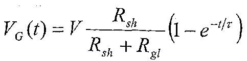
여기에서, τ=[(CRshRgl)/Rsh+Rgl)]=CReq이고 Req는 병렬 등가 저항이다. VG는 전방 EVA 인캡슐런트 상의 전압으로서 금속산화물 반도체(MOS) 트랜지스터의 게이트와 같이 동작한다. MOS 트랜지스터의 게이트 산화물은 산화물 유전체 패시베이션 층이다. 언급된 바와 같이, 커패시턴스 "C"는 질화물 ARC, 산화물 패시베이션 층, 및 실리콘 웨이퍼로 형성된 커패시터를 나타낸다.Where τ = [(CR sh R gl ) / R sh + R gl )] = CR eq and R eq is the parallel equivalent resistance. V G acts like the gate of a metal oxide semiconductor (MOS) transistor as the voltage on the front EVA encapsulant. The gate oxide of the MOS transistor is an oxide dielectric passivation layer. As mentioned, capacitance "C" refers to a capacitor formed of nitride ARC, oxide passivation layer, and silicon wafer.
태양전지의 파워 업 시, 게이트(즉, 전방측 EVA 인캡슐런트)는 위로 램프되어 수학식 2에 의해 표현되는 저하 시간 tdeg 이후에 특정 저하량을 유발하는 전압 VT에 도달할 것이다.Upon power up of the solar cell, the gate (ie, the front EVA encapsulant) will ramp up to reach a voltage V T which causes a certain amount of degradation after the degradation time t deg represented by Equation 2.

수학식 2에서, "V"는 양인 것으로 가정되지만, 전압에 대한 절대값이 이용되는 경우에 음의 V 및 음의 VT(MOS 트랜지스터의 임계 전압)에도 적용된다. V[(Rsh)/(Rgl+Rsh)] ≫VT인 통상의 경우에 대해, 수학식 2는 수학식 3으로 줄어든다.In Equation 2, " V " is assumed to be positive, but is also applied to negative V 占 ° negative V T (threshold voltage of the MOS transistor) when absolute values for voltage are used. For the normal case where V [(R sh ) / (R gl + R sh )] '' V T , equation (2) is reduced to equation (3).
![]()
![]()
수학식 3으로부터, 고전압에 대해, 특정 저하량까지의 시간은 인가 전압에 반비례한다는 것을 쉽게 알 수 있다.From Equation 3, it can be easily seen that, for a high voltage, the time to a specific decrease amount is inversely proportional to the applied voltage.
제로 인가 전압의 복원은 수학식 4에 의해 주어진다.The restoration of the zero applied voltage is given by equation (4).
![]()
![]()
VT가 무시가능한 저하가 발생하는 임계인 경우, 복원 시간 trec는 수학식 5에 의해 주어진다.If V T is the threshold at which negligible degradation occurs, the recovery time t rec is given by equation (5).

자외선광은 현재의 것과 병렬로 추가 션트 저항을 추가시키는 효과를 가질 것이다. 이것은 질화물 ARC로부터 실리콘 웨이퍼에 자외선이 전자를 주입하는 비율이 트랩된 전자 밀도에 비례한다는 가정에 의해 알 수 있다. 그러나, 커패시터 "C"(도 3b 참조)의 양단 전압은 트랩된 전하에 비례하고, 따라서 전류는 게이트 커패시터 상의 전압, 즉 저항-등에 비례한다. 이러한 저항이 다른 션트(효과를 가지기 위해서는 반드시 존재해야 함)에 비해 때 작다고 가정하면, 광의 복원 시간 trec , light는 수학식 6에 의해 주어진다.Ultraviolet light will have the effect of adding additional shunt resistance in parallel with the current one. This can be seen by the assumption that the rate at which ultraviolet light injects electrons from the nitride ARC into the silicon wafer is proportional to the trapped electron density. However, the voltage across capacitor " C " (see FIG. 3B) is proportional to the trapped charge, so the current is proportional to the voltage on the gate capacitor, i. Assuming that this resistance is small when compared to other shunts (which must be present to have an effect), the recovery time t rec , light of light is given by:

자외선 유도된 션트가 태양전지 모듈이 저하되는 것을 방지할만큼 충분하도록 필요한 조건이 계산될 수 있다. 이것은 수학식 7에 의해 주어진 조건이 만족되는 것을 요구한다.The necessary conditions can be calculated such that the ultraviolet induced shunt is sufficient to prevent the solar cell module from deteriorating. This requires that the condition given by equation (7) is satisfied.

상기 수학식은 광의 복원 시간이 수학식 8에 의해 주어지는 경우에 수학식 7이 만족되는 것을 보여주도록 배열될 수 있다.Equation 7 may be arranged to show that Equation 7 is satisfied when the recovery time of light is given by Equation 8.

환언하면, 바이어싱되지 않은 때에, 태양전지 모듈이 인가된 바이어스로 어두움에서 저하되는데 걸리는 것보다 더 짧은 시간에 햇빛에서 복원하는 경우, 모듈은 그 인가된 바이어스로 햇빛에서 안정될 것이다.In other words, when unbiased, if the solar cell module recovers from sunlight in a shorter time than it takes to degrade in the dark with an applied bias, the module will be stabilized in the sunlight with that applied bias.
일부 실시예들에서, 전방측 반사 방지 코팅/패시베이션 층 스택에서 수직 전기 전도도를 증가시킴으로써 유해한 태양전지 분극화가 방지되거나 최소화된다. 이들 실시예들에서, 전하는 태양전지의 전방측으로부터 웨이퍼의 몸체로 흘러나온다. 이들 실시예들은 도 4a 및 4b를 참조하여 이제 설명된다.In some embodiments, harmful solar cell polarization is prevented or minimized by increasing vertical electrical conductivity in the front antireflective coating / passivation layer stack. In these embodiments, charge flows from the front side of the solar cell into the body of the wafer. These embodiments are now described with reference to FIGS. 4A and 4B.
도 4a는 본 발명의 실시예에 다른 태양전지(200A)의 단면을 개략적으로 도시하고 있다. 태양전지(200A)는 도 2에 도시된 태양전지(200)의 특정 실시예이다. 태양전지(200A)는 패시베이션 층(202)으로서 매우 얇은 산화물(즉, 실리콘 다이옥사이드) 층(202A) 및 반사 방지 코팅(201)으로서 반사 방지 코팅(201A)의 이용을 제외하고는 태양전지(200)와 동일하다. 도 4a의 예에서, 반사 방지 코팅(201A)은 약 400Å의 두께를 가지는 실리콘 카바이드를 포함하고, 웨이퍼(203)는 N형 실리콘 웨이퍼를 포함한다. 얇은 산화물 층(202A)은 양호하게는 웨이퍼의 몸체에 전하를 흘러들이게 하고, 전하 구축(buildup)을 방지할 만큼 충분히 얇고, 따라서 비교적 높은 전압을 생성할 때 산화물 브레이크다운이 발생한다. 얇은 산화물 층(202A)은 웨이퍼(203) 상에 바로 형성된다. 하나의 실시예에서, 얇은 산화물 층(202A)은 이온제거된 물에 부유된 오존을 포함하는 배스(bath)에 웨이퍼(203)를 담그는 것과 관련된 오존 산화물 프로세스를 이용하여 약 10Å 내지 20Å의 두께로 형성된다.4A schematically illustrates a cross section of a
도 4b는 본 발명의 실시예에 따른 태양전지(200B)의 단면을 개략적으로 도시하고 있다. 태양전지(200B)는 도 2에 도시된 태양전지(200)의 특정 실시예이다. 태양전지(200B)는 패시베이션 레벨(202)로서 패터닝된 유전체 패시베이션 층(202B)의 이용을 제외하고는 태양전지(200)와 동일하다. 도 4b의 예에서, 패시베이션 층(202B)은 실리콘 다이옥사이드를 포함하고, 반사 방지 코팅(201)은 실리콘 질화물을 포함하며, 웨이퍼(203)는 N-형 실리콘 웨이퍼를 포함한다. 도 4b에 도시된 바와 같이, 패시베이션 층(202B)은 실리콘 질화물 반사 방지 코팅(201)이 실리콘 웨이퍼(203)를 접촉하도록 허용하는 홀을 가지도록 패터닝되었다. 이것은 반사 방지 코팅(201) 상의 전하가 산화물 패시베이션 층(202B)의 패터닝된 홀을 통해 웨이퍼(203)의 몸체로 흘러가도록 허용한다. 패시베이션 층(202B)의 각 홀은 종래의 리소그래피 프로세스를 이용하여 형성되고, 가용한 리소그래피 장비가 허용하는 만큼 작다. 패터닝된 홀은 예를 들면 서로 약 0.1mm 내지 약 2.0mm만큼 분리된다. 관통된 패시베이션 층(202B)은 양호하게는 반사 방지 코팅(201)에서의 전하 구축(buil up)을 방지함으로써 태양전지 분극화를 방지한다.4B schematically illustrates a cross section of a
일부 실시예들에서, 태양전지의 전방측 상에서 에지를 향한 횡방향 전도는 태양전지 분극화를 방지하도록 증가된다. 패시베이션 층은 그들을 통해 자연적 결함(즉, 자연적으로 형성된 홀)을 가지고 있으므로, 도전성 반사 방지 코팅은 결함을 통해 웨이퍼의 몸체로 누적된 전하를 흐르게 할 수 있다. 그러나, 일부 태양전지 반사 방지 코팅은 이것이 발생하기 충분할 만큼 도전성이지 않을 수 있다. 따라서, 일부 실시예들에서, 도전층은 반사 방지 코팅을 접촉하도록 횡방향으로 형성되어, 전하가 도전층 및 패시베이션 층의 결함을 통해 반사 방지 코팅으로부터 웨이퍼의 몸체로 흐르도록 허용한다. 다른 실시예들에서, 반사 방지 코팅 자체는 충분히 도전성이다. 이제, 이들 실시예들은 도 5a-5d를 참조하여 설명된다.In some embodiments, the transverse conduction towards the edge on the front side of the solar cell is increased to prevent solar cell polarization. Since the passivation layer has natural defects (ie, naturally formed holes) through them, the conductive antireflective coating can flow accumulated charges through the defects into the body of the wafer. However, some solar cell antireflective coatings may not be conductive enough to cause this to occur. Thus, in some embodiments, the conductive layer is formed laterally to contact the antireflective coating, allowing charge to flow from the antireflective coating to the body of the wafer through defects in the conductive and passivation layers. In other embodiments, the antireflective coating itself is sufficiently conductive. These embodiments are now described with reference to FIGS. 5A-5D.
도 5a는 본 발명의 실시예에 따른 태양전지(200C)의 단면을 개략적으로 도시하고 있다. 태양전지(200C)는 도 2에 도시된 태양전지(200)의 특정 실시예이다. 태양전지(200C)는 투명한 도전성 코팅(501)이 반사 방지 코팅(201)의 상부 표면 상에 형성되어 있다는 점을 제외하고는 태양전지(200)와 동일하다. 도 5a의 예에서, 패시베이션 층(202)은 실리콘 다이옥사이드를 포함하고, 반사 방지 코팅(201)은 실리콘 질화물을 포함하며, 웨이퍼(203)는 N-형 실리콘 웨이퍼를 포함한다. 하나의 실시예에서, 투명 도전성 코팅(501)은 PEDOT/PSS(베이트론-P) 코팅과 같은 도전성 유기 코팅을 포함한다. 투명 도전성 코팅(501)은 반사 방지 코팅(201)의 상부 상에 바로 스프레이되거나 스크린-인쇄된다. 투명 도전성 코팅(501)은 예를 들면, 약 100Å의 두께로 형성될 수 있다. 투명 도전성 코팅(501)은 인캡슐레이션 바로 이전에, 태양전지 제조 프로세스의 최종 단계로서 태양전지(200) 상에 적용될 수 있다.5A schematically illustrates a cross section of a
실리콘 질화물 반사 방지 코팅(201)이 충분히 도전성이지 않으므로, 실리콘 질화물의 전하는 짧은 거리만을 이동할 수 있고, 이는 패시베이션 층(202)에서 자연적 결함에 도달할만큼 충분하지 않다. 투명 도전성 코팅(501)은 반사 방지 코팅(201)의 전하가 패시베이션 층(202)의 자연적 결함에 도달하기에 충분한 거리를 이동하고 웨이퍼(203)의 몸체로 흐를 수 있게 한다.Since silicon
도 5b는 본 발명의 실시예에 따른 태양전지(200D)의 단면을 개략적으로 도시하고 있다. 태양전지(200D)는 도 2에 도시된 태양전지(200)의 특정 실시예이다. 태양전지(200D)는 도전성 반사 방지 코팅(ARC, 201B)이 반사 방지 코팅(201)으로서 이용되는 것을 제외하고는 태양전지(200)와 동일하다. 도 5b의 예에서, 패시베이션 층(202)은 실리콘 다이옥사이드를 포함하고, 웨이퍼(203)는 N-형 실리콘 웨이퍼를 포함한다. 도전성 ARC(201B)는 양호하게는 전하가 그 안에 누적되는 것을 방지함으로써 태양전지 분극화를 최소화시킨다. 도전성 ARC(201B)의 전하는 패시베이션 층(202)의 자연적 결함을 통해 웨이퍼의 몸체로 흐를 수 있다.5B schematically illustrates a cross section of a
하나의 실시예에서, 도전성 ARC(201B)는 산화 티타늄(TiO2)과 같이 본질적으로 도전성인(즉, 불순물의 추가 없이 도전성인) 반사 방지 코팅을 포함한다.In one embodiment,
다른 실시예들에서, 도전성 ARC(201B)는 불순물의 추가에 의해 도전성이 되는 비-도전성 반사 방지 재료를 포함한다. 그렇게 하는 하나의 방법은 패시베이션 층(202) 상의 반사 방지 재료의 형성 동안에 금속 기체 소스로부터 금속 불순물을 추가하는 것이다. 예를 들면, 도전성 ARC(201B)는 불소로 도핑된 주석 산화 물(SnO:F), 브롬으로 도핑된 아연 산화물(ZnO:B), 또는 인 또는 브롬으로 도핑된 실리콘 카바이드(SiC:P 또는 SiC:B)를 포함한다. 특정 예로서, 도전성 ARC(201B)는 피착 동안에 인화수소 기체(PH3) 또는 디보란 기체(B2H6)의 추가로 실리콘 카바이드(SiC)의 플라즈마 인핸스드 화학적 증착(PECVD)에 의해 약 400Å의 두께로 형성될 수 있다. In other embodiments,
도 5c는 본 발명의 실시예에 따른 태양전지(200E)의 단면을 개략적으로 도시하고 있다. 태양전지(200E)는 도 2에 도시된 태양전지(200)의 특정 실시예이다. 태양전지(200E)는 투명 도전층(502)이 반사 방지 코팅(201)의 상부 상에 형성된다는 것을 제외하고는 태양전지(200)와 동일하다. 도 5c의 예에서, 패시베이션 층(202)은 실리콘 다이옥사이드를 포함하고, 반사 방지 코팅(201)은 실리콘 질화물을 포함하며, 실리콘 웨이퍼(203)는 N-형 웨이퍼를 포함한다. 태양전지(200c, 도 5a)의 도전성 코팅(501)과 같이, 투명 도전층(502)은 반사 방지 코팅(201)의 전하가 패시베이션 층(202)의 자연적 결함에 도달하기에 충분한 거리를 이동하여 웨이퍼(203)의 몸체에 흐르도록 허용한다.5C schematically illustrates a cross section of a
투명 도전층(502)은 반사 방지 코팅(201)의 상부 바로 위에 증발되거나, 스퍼터링되거나 피착된다. 투명 도전층(502)은 약 200Å의 두께로 형성된, 불소로 도핑된 주석 산화물(SnO:F), 브롬으로 도핑된 아연 산화물(ZnO:B), 또는 인 또는 브롬으로 도핑된 실리콘 카바이드(SiC:P, 또는 SiC:B)와 같은 투명 도전성 산화물을 포함할 수 있다.The transparent
도 5d는 본 발명의 실시예에 따른 태양전지(200F)의 단면을 개략적으로 도시하고 있다. 태양전지(200F)는 도 2에 도시된 태양전지(200)의 특정 실시예이다. 태양전지(200F)는 비교적 얇은(예를 들면, 약 200Å) 도전층(503)이 패시베이션 층(202)과 반사 방지 코팅(201)의 사이에 형성된다는 점을 제외하고는 태양전지(200)와 동일하다. 도 5d의 예에서, 패시베이션 층(202)은 실리콘 다이옥사이드를 포함하고, 반사 방지 코팅(201)은 실리콘 질화물을 포함하며, 실리콘 웨이퍼(203)는 N-형 웨이퍼를 포함한다. 얇은 도전층(503)은 전하가 반사 방지 코팅(201)으로부터 얇은 도전층(503)으로, 그리고 패시베이션 층(202)의 자연적 결함을 통해 웨이퍼(203)의 몸체로 흐를 수 있게 한다. 하나의 실시예에서, 도전층(503)은 패시베이션 층(202)의 상부 표면 상에 바로 약 200Å의 두께로 형성된 폴리실리콘을 포함한다. 반사 방지 코팅(201)은 도전층(503)의 표면 상에 바로 형성될 수 있다. 도전층(503)은 PECVD에 의해, 그리고 반사 방지 코팅(201)의 형성으로 제자리에서(즉, 한번의 로딩시에 동일한 챔버 또는 클러스터 내에서) 형성될 수 있다. 도전층(503)은 약 200Å의 두께로 형성된, 불소로 도핑된 주석 산화물(SnO:F), 브롬으로 도핑된 아연 산화물(ZnO:B), 또는 인 또는 브롬으로 도핑된 실리콘 카바이드(SiC:P, SiC:B)를 포함할 수도 있다.5D schematically illustrates a cross section of a
도 4 및 도 5의 실시예에서, 태양전지의 전방측으로부터 웨이퍼의 몸체로의 전도도가 증가되어 유해한 태양전지 분극화를 방지한다. 이것은 도 3b의 모델에서 션트 저항 Rsh를 낮추는 것과 등가이다. 다른 실시예들에서, 태양전지의 전방측으 로부터 투명 커버를 통한 모델의 나머지로의 저항이 증가되어 전하 누설을 방지한다. 이것은 도 3b의 모델에서 저항 Rgl을 증가시키는 것과 등가이다. 태양전지의 전방측으로부터 태양전지의 나머지까지의 저항은 이제 도 6을 참조하여 설명되는 바와 같이, 전하 누설 경로를 차단함으로써 증가될 수 있다.4 and 5, the conductivity from the front side of the solar cell to the body of the wafer is increased to prevent harmful solar cell polarization. This is equivalent to lowering the shunt resistor R sh in the model of FIG. 3B. In other embodiments, the resistance from the front side of the solar cell to the rest of the model through the transparent cover is increased to prevent charge leakage. This is equivalent to increasing the resistance R gl in the model of FIG. 3B. The resistance from the front side of the solar cell to the rest of the solar cell can be increased by blocking the charge leakage path, as now described with reference to FIG. 6.
도 6은 본 발명의 실시예에 따른 태양전지(200G)의 단면을 개략적으로 도시하고 있다. 태양전지(200G)는 도 2에 도시된 태양전지(200)의 특정 실시예이다. 태양전지(200G)는 투명 전기 절연체층(691)이 반사 방지 코팅(201) 위에 형성된다는 점을 제외하고는 태양전지(200)와 동일하다. 도 6의 예에서, 패시베이션 층(202)은 실리콘 다이옥사이드를 포함하고, 반사 방지 코팅(201)은 실리콘 질화물을 포함하며, 실리콘 웨이퍼(203)는 N-형 웨이퍼를 포함한다. 전기 절연체층(691)은 반사 방지 코팅(201) 위에 형성되어 전하가 태양전지(200G)의 전방측으로부터 커버(104, 도 2 참조)를 향하여 누설되는 것을 방지함으로써 태양전지 분극화를 방지한다. 하나의 실시예에서, 전기 절연체층(691)은 대기압 화학적 증착(APCVD)에 의해 약 0.1 내지 1.0㎛의 두께로 형성된 실리콘 다이옥사이드(SiO2)를 포함한다.6 schematically illustrates a cross section of a
유해한 태양전지 분극화는 이제 도 7a를 참조하여 설명되는 바와 같이, 태양전지의 전방측 상의 태양전지 모듈의 영역을 바이어싱함으로써 방지될 수 있다.Harmful solar cell polarization can now be prevented by biasing the area of the solar cell module on the front side of the solar cell, as described with reference to FIG. 7A.
도 7a는 본 발명의 실시에에 따른 태양전지 모듈(100A)을 개략적으로 도시하고 있다. 태양전지 모듈(100A)은 도 2에 도시된 태양전지 모듈(100)의 특정 실시예이다. 그 인터커넥트(682)와 함께, 수 개의 태양전지(200)가 도 7a에 도시되어 있다. 인터커넥트(682)는 하나의 태양전지(200)를 다른 하나에 직렬로 접속시킨다. 태양전지 모듈(100A)은 전기적 도전성 경로가 유해한 누설 전류를 방지하도록 셀 전방에 모듈의 일부의 전위(즉, n형 셀 모듈에 대해 30V 이상, 그 값 또는 그 이내)를 상승시키도록 부가된다는 점을 제외하고는 태양전지 모듈(100)과 실질적으로 동일하다. 하나의 실시예에서, 도전성 경로는 투명 전기적 도전층(684)을 투명 커버(104, 예를 들면 유리)의 후방 표면 상에 배치하고 도전층(684)을 태양전지(200)의 후방 표면에 접속함으로써 형성된다. 도 7a의 예에서, 도전층(684)은 전기적 접속(683)을 통해 태양전지(200)의 후방측에 접속되는 인터커넥트(682)에 전기적으로 접속된다. 도 7a의 예에서, 양호한 실시예는 n형 전방측 확산 영역을 가지는 셀에 대해 어레이의 최고(즉, 최대 양의) 또는 최고 근처의 전위 태양전지(200)에, 그리고 p형 전방측 확산 영역을 가지는 셀에 대해 어레이에서 가장 낮은(즉, 최대 음의) 또는 최대 음의 전위 근처인 태양전지(200)에 접속되는 인터커넥트(682)에 도전층(684)이 접속되는 것이다. 도전층(684)은 태양전지 모듈(100A)의 프레임으로부터 분리되어 고전압이 모듈의 외부 상에 존재하는 불안전한 조건을 방지한다. 도전층(684)은 불소로 도핑된 주석 산화물(SnO:F), 인듐 주석 산화물(ITO), 아연 산화물(ZnO) 또는 다른 투명 산화물 또는 투명 유기 도전체를 포함한다. 양호한 실시예에서, 이러한 도전층은 약 5e4 Ω/□의 시트 저항을 가지고 있다. 후방 시트(102)는 이전과 같이 인캡슐런트(103)의 기저 표면 상에 형성된다. 다른 실시예에서, 인캡슐런트(103)는 전기적으로 도전성으로 만들어져, 태양전지(100) 상에 거의-등전위 필드를 형성하고, 모듈의 에지에서의 인캡슐런트는 전기적으로 절연 상태로 유지되어 고전압이 모듈의 외부에 존재하는 불안전한 조건을 방지한다.7A schematically illustrates a
시스템 레벨 접근법에서, 전체 태양에너지 시스템이 고려되어 전하가 태양전지의 전방측으로부터 누설되는 것을 방지한다. 예를 들면, 태양전지 모듈의 어레이는 태양전지의 전방측으로부터의 전하 캐리어의 누설이 방지되도록 바이어싱될 수 있다. 태양전지 분극화 문제에 대한 시스템 레벨 접근법의 예는 이제 도 7b 및 7c를 참조하여 설명된다.In a system level approach, the entire solar energy system is considered to prevent charge from leaking from the front side of the solar cell. For example, the array of solar cell modules can be biased to prevent leakage of charge carriers from the front side of the solar cell. An example of a system level approach to the solar cell polarization problem is now described with reference to FIGS. 7B and 7C.
도 7b는 본 발명의 실시예에 따른 태양 에너지 시스템(790)을 개략적으로 예시하고 있다. 도 7b의 예에서, 태양전지 모듈 어레이(630)는 상호접속된 태양전지(200)를 포함하는 수 개의 태양전지 모듈을 구비하고 있다. 태양전지 모듈 어레이(630)의 양의 출력 단자는 노드(616)로 라벨링되고, 그 음의 출력 단자는 노드(617)로 라벨링된다. 도 7b의 예에서, 태양전지(200)는 그 양의 단자가 노드(616)를 향하고 그 음의 단자가 노드(617)를 향하도록 병렬 접속된다. 도 7b에 도시된 직렬에 병렬로 다른 직렬 접속된 태양전지(200)가 있을 수 있다.7B schematically illustrates a
도 7b의 예에서, 태양전지 모듈 어레이(630)는 인버터(600)에 결합된다. 인버터는 직류(DC)를 교류(AC)로 전환한다. 태양에너지 시스템(790)에서, 인버터(600)는 태양전지 모듈 어레이(630)로부터 직류를 수신하고, 전력 그리드에 교류를 출력한다. 도 7b에 도시된 바와 같이, DC 대 DC 컨버터(601)는 태양전지 모듈 어레이(630)로부터의 직류를 다른 직류로 전환시킨다. DC 대 DC 컨버터(601)의 직류 출력은 DC 대 AC 컨버터(602)에 의해 교류로 전환된다. DC 대 AC 컨버터(602) 의 교류 전류 출력은 분리 회로(603)를 통해 전력 그리드에 제공된다. 다르게는, 분리 회로(603)는 DC 대 DC 컨버터(601)와 DC 대 AC 컨버터(602)의 사이에 직렬로 존재할 수 있다.In the example of FIG. 7B, the solar
태양 에너지 시스템(790)에서, 태양전지 어레이 모듈(630)의 양의 단자는 그라운딩된다. 태양 에너지 시스템(790)과 유사한 시스템은 다른 나라들 중에서도 북미 및 일본에서 이용된다. 태양전지 모듈 어레이(630)의 모든 태양전지 모듈의 프레임을 나타내는 프레임(614)은 또한 라벨(611)로 나타낸 바와 같이 그라운딩된다. 태양전지 모듈 어레이(630)의 양의 단자 및 프레임(614)을 그라운딩하는 것은 태양전지(200)와 프레임(614)간의 전위를 감소시켜, 태양전지(200)의 전방측으로부터의 누설을 최소화시킨다. 태양전지 모듈 어레이(630)의 양의 단자는 인버터(600)의 내부 또는 외부에서 그라운드로 묶여진다.In
도 7b의 예에서, 각 태양전지(200)는 n형 전방측 확산 영역을 가지고 있다. 이 경우에, 태양전지(200)가 그라운드에 비해 양으로 바이어싱되게 되므로 유해한 태양전지 분극화가 발생한다. 유해한 분극화를 방지하기 위해, 따라서 태양전지 모듈 어레이(630, 이 경우에는 노드(616))의 최고 또는 최고 근처의 전위가 그라운드로 묶여진다. 태양전지가 p형 전방측 확산 영역을 가지는 다른 실시예들에서, 태양전지가 그라운드에 비해 음으로 바이어싱되게 되는 경우에 유해한 분극화가 발생한다. 그 경우에, 어레이의 최저 또는 최저 근처의 전위 태양전지(예를 들면, 태양전지 모듈 어레이의 음의 출력 단자)는 그라운드로 묶여 유해한 태양전지 분극화를 방지시킨다.In the example of FIG. 7B, each
도 7c는 본 발명의 실시예에 따른 태양 에너지 시스템(795)을 개략적으로 예시하고 있다. 도 7c의 예에서, 태양전지 모듈 어레이(630)는 수개의 상호 접속된 태양전지(200)를 포함하는 수 개의 태양전지 모듈을 가지고 있다. 태양전지 모듈 어레이(630)의 양의 출력 단자는 노드(616)로 라벨링되고, 그 음의 출력 단자는 노드(617)로 라벨링된다. 도 7c의 예에서, 태양전지(200)는 그 양의 단자가 노드(616)를 향하고 그 음의 단자가 노드(617)를 향하도록 직렬 접속된다. 도 7c에 도시된 직렬에 병렬로 다른 직렬 접속된 태양전지(200)가 있다.7C schematically illustrates a
도 7c의 예에서, 태양전지 모듈 어레이(630)는 인버터(650)에 결합된다. 인버터(650)는 태양전지 모듈 어레이(630)로부터 직류를 수신하고, 전력 그리드에 교류를 출력한다. 도 7c에 도시된 바와 같이, DC 대 DC 컨버터(651)는 태양전지 모듈 어레이(630)로부터의 직류를 다른 직류로 전환시킨다. DC 대 DC 컨버터(651)의 직류 출력은 분리 회로(653)에 의해 DC 대 AC 컨버터(652)에 결합된다. DC 대 AC 컨버터(652)의 교류 출력은 전력 그리드에 제공된다. 다르게는, 분리 회로(653)는 DC 대 AC 컨버터(652)의 출력에 배치되어, AC 출력을 전력 그리드에 제공한다. 태양 에너지 시스템(795)과 유사한 시스템은 대부분의 유럽 국가, 영국 등과 같은 IEC 규정에 의해 커버되는 국가들에서 채용될 수 있다.In the example of FIG. 7C, solar
도 7c의 예에서, 태양전지 어레이 모듈(630)의 출력은 태양전지 모듈 어레이(630)의 전체 전압값의 +/- 1/2(즉, 플러스/마이너스 절반)로 밸런싱된다. 즉, 노드(616)에서의 전압은 이상적으로는 태양전지 모듈 어레이(630)의 전체 전압의 +1/2이고, 노드(617)에서의 전압은 이상적으로는 태양전지 어레이 모듈(630)의 전 체 전압의 -1/2이다. 저항기(672, 673)는 그라운드 포인트 주위에서 태양전지 모듈 어레이(630)의 출력을 밸런싱하는 높은 값 저항기(또는 바리스터)이다. 실제로, 태양전지 모듈 어레이(630)의 출력은 밸런싱 저항기(672, 673)가 높은 저항(예를 들면, 각각 약 10㏁)을 가지고 있으므로 근사적으로만 밸런싱된다.In the example of FIG. 7C, the output of the solar
전형적인 설치시, 태양전지 모듈 어레이(630)는 저항기(671)가 존재하지 않고 인버터가 태양전지 모듈 어레이(630)의 출력과 전력 그리드로의 AC 출력간의 DC-DC 분리를 가지고 있으므로 플로팅할 것이다. 그러나, 본 발명자들은, 그러한 설치가 태양전지(200)의 유해한 분극화를 유발할 것이라는 것을 발견했다. 하나의 실시예에서, 태양전지 모듈 어레이(630)의 양의 단자는 저항기(671)에 의해 그라운드에 접속된다. 저항기(671)는 본 발명의 장점을 줄이지 않고, 고정되거나, 가변되거나 또는 전자적으로 제어되는 저항일 수 있다. 저항기(671)는 태양전지 모듈 어레이(630)를 그 출력의 양의 측에 더 근접하여 바이어싱하여, 양의 전하가 태양전지(200)의 전방측으로부터 누설되는 것을 방지한다. 환언하면, 저항기(671)는 태양전지 모듈 어레이(630)의 출력을 양을 향하여 "언밸런싱시켜", 태양전지 분극화를 방지한다. 유사하게, 태양전지 분극화가 태양전지(200)의 전방측으로부터 누설되는 전자(양의 전하라기보다는)에 의해 야기되는 경우, 노드(617, 노드(616) 대신)가 저항기(671)를 통해 그라운드에 접속되어, 태양전지 모듈 어레이(630)를 그 음의 출력을 향하여 바이어싱시킨다. 저항기(671)는 밸런싱 저항기(즉, 저항기(672 또는 673))의 값의 약 ≤ 1/10인 저항을 가질 수 있다. 유의할 점은, 누설 전하 캐리어(즉, 전자 또는 홀)의 극성에 따라, 태양전지 모듈 어레이(630)의 밸런 싱된 출력을 양 또는 음을 향하여 언밸런싱시키도록 구성될 수 있다는 점이다. 예를 들면, 저항기(672)의 값은 저항기(673)에 비해 증가되어, 저항기(671)를 이용하지 않고서도 태양전지 모듈 어레이(630)의 출력을 언밸런싱시킨다.In a typical installation, the solar
저항기(671)는 전자적으로 제어되는 저항을 또한 포함한다. 예를 들면, 저항기(671)의 저항은 조건에 따라 다른 저항값으로 스위칭함으로써 전자 회로에 의해 제어될 수 있다. 그러한 전자 회로는 예를 들면 비가 오는 때와 같이, 태양전지 모듈 어레이 저항이 그라운드 레벨로 감소되는 경우에 더 낮은 저항이 필요한 때를 감지하는 센서를 가질 수 있다.
도 7c의 예에서, 각 태양전지(200)는 n형 전방측 확산 영역을 가지고 있다. 이 경우에, 유해한 태양전지 분극화는 태양전지(200)가 그라운드에 비해 양으로 바이어싱되기 때문에 발생한다. 유해한 분극화를 방지하기 위해, 따라서 태양전지 모듈 어레이(630, 이 경우에, 노드(616))의 최고 또는 최고 근처의 전위가 저항(예를 들면, 저항기(671))을 통해 그라운드에 묶여진다. 태양전지가 p형 전방측 확산 영역을 가지는 다른 실시예들에서, 태양전지가 그라운드에 비해 음으로 바이어싱되는 경우에 유해한 분극화가 발생한다. 그 경우에, 어레이의 최저 또는 최저 근처의 전위 태양전지(예를 들면, 태양전지 모듈 어레이의 음의 출력 단자)는 저항에 의해 그라운드로 묶여, 유해한 태양전지 분극화를 방지한다.In the example of FIG. 7C, each
유해한 태양전지 분극화를 방지하기 위한 기술이 개시되어 있다. 본 발명의 특정 실시예들이 제공되었지만, 이들 실시예들은 예시의 목적을 위한 것으로 제한을 위한 것이 아니라는 것은 자명하다. 다수의 추가 실시예들은 본 공보를 읽는 본 기술분야의 통상의 기술자들에게는 명백할 것이다.A technique for preventing harmful solar cell polarization is disclosed. While certain embodiments of the invention have been presented, it is obvious that these embodiments are for purposes of illustration and not limitation. Many additional embodiments will be apparent to those of ordinary skill in the art reading this publication.
Claims (19)
Applications Claiming Priority (5)
| Application Number | Priority Date | Filing Date | Title |
|---|---|---|---|
| US65870605P | 2005-03-03 | 2005-03-03 | |
| US60/658,706 | 2005-03-03 | ||
| US11/210,213 US7554031B2 (en) | 2005-03-03 | 2005-08-22 | Preventing harmful polarization of solar cells |
| US11/210,213 | 2005-08-22 | ||
| PCT/US2006/002137 WO2006096247A2 (en) | 2005-03-03 | 2006-01-20 | Preventing harmful polarization of solar cells |
Related Child Applications (1)
| Application Number | Title | Priority Date | Filing Date |
|---|---|---|---|
| KR1020097007569A Division KR101080583B1 (en) | 2005-03-03 | 2006-01-20 | Preventing harmful polarization of solar cells |
Publications (2)
| Publication Number | Publication Date |
|---|---|
| KR20070105341A KR20070105341A (en) | 2007-10-30 |
| KR100933598B1 true KR100933598B1 (en) | 2009-12-23 |
Family
ID=36942960
Family Applications (2)
| Application Number | Title | Priority Date | Filing Date |
|---|---|---|---|
| KR1020077019044A KR100933598B1 (en) | 2005-03-03 | 2006-01-20 | Prevention of harmful polarization of solar cells |
| KR1020097007569A KR101080583B1 (en) | 2005-03-03 | 2006-01-20 | Preventing harmful polarization of solar cells |
Family Applications After (1)
| Application Number | Title | Priority Date | Filing Date |
|---|---|---|---|
| KR1020097007569A KR101080583B1 (en) | 2005-03-03 | 2006-01-20 | Preventing harmful polarization of solar cells |
Country Status (6)
| Country | Link |
|---|---|
| US (7) | US7554031B2 (en) |
| EP (1) | EP1854147B1 (en) |
| JP (4) | JP5224444B2 (en) |
| KR (2) | KR100933598B1 (en) |
| CN (4) | CN102194911B (en) |
| WO (1) | WO2006096247A2 (en) |
Families Citing this family (149)
| Publication number | Priority date | Publication date | Assignee | Title |
|---|---|---|---|---|
| US7554031B2 (en) * | 2005-03-03 | 2009-06-30 | Sunpower Corporation | Preventing harmful polarization of solar cells |
| JP4200339B2 (en) * | 2005-09-29 | 2008-12-24 | マイクロシリトロン株式会社 | Fuel cell unit cell, fuel cell unit cell array, fuel cell module, and fuel cell system |
| GB2442254A (en) * | 2006-09-29 | 2008-04-02 | Renewable Energy Corp Asa | Back contacted solar cell |
| US20080135092A1 (en) * | 2006-12-11 | 2008-06-12 | Sunmodular, Inc. | Solar roof tiles with heat exchange |
| US20080134497A1 (en) * | 2006-12-11 | 2008-06-12 | Sunmodular, Inc. | Modular solar panels with heat exchange & methods of making thereof |
| US7728219B2 (en) * | 2006-12-11 | 2010-06-01 | Sunmodular, Inc. | Photovoltaic cells, modules and methods of making same |
| WO2008098407A1 (en) * | 2007-02-08 | 2008-08-21 | Suntech Power Co., Ltd | Hybrid silicon solar cells and method of fabricating same |
| JP5687837B2 (en) * | 2007-02-16 | 2015-03-25 | ナノグラム・コーポレイションNanoGram Corporation | Solar cell structure, photovoltaic module and methods corresponding thereto |
| US7670638B2 (en) * | 2007-05-17 | 2010-03-02 | Sunpower Corporation | Protection layer for fabricating a solar cell |
| US7838062B2 (en) * | 2007-05-29 | 2010-11-23 | Sunpower Corporation | Array of small contacts for solar cell fabrication |
| US8294296B2 (en) * | 2007-08-03 | 2012-10-23 | Advanced Energy Industries, Inc. | System, method, and apparatus for remotely coupling photovoltaic arrays |
| US20090217964A1 (en) * | 2007-09-26 | 2009-09-03 | Advanced Energy Industries, Inc. | Device, system, and method for improving the efficiency of solar panels |
| US20090078304A1 (en) * | 2007-09-26 | 2009-03-26 | Jack Arthur Gilmore | Photovoltaic charge abatement device, system, and method |
| US8987039B2 (en) | 2007-10-12 | 2015-03-24 | Air Products And Chemicals, Inc. | Antireflective coatings for photovoltaic applications |
| DE102007054384A1 (en) | 2007-11-14 | 2009-05-20 | Institut Für Solarenergieforschung Gmbh | Method for producing a solar cell with a surface-passivating dielectric double layer and corresponding solar cell |
| US8198528B2 (en) * | 2007-12-14 | 2012-06-12 | Sunpower Corporation | Anti-reflective coating with high optical absorption layer for backside contact solar cells |
| KR20090067350A (en) * | 2007-12-21 | 2009-06-25 | 주성엔지니어링(주) | Thin film type solar cell and method for manufacturing the same |
| WO2009098241A1 (en) * | 2008-02-05 | 2009-08-13 | Oerlikon Trading Ag, Trübbach | Encapsulation of optoelectronic devices |
| US8440903B1 (en) * | 2008-02-21 | 2013-05-14 | Stion Corporation | Method and structure for forming module using a powder coating and thermal treatment process |
| US20090211627A1 (en) * | 2008-02-25 | 2009-08-27 | Suniva, Inc. | Solar cell having crystalline silicon p-n homojunction and amorphous silicon heterojunctions for surface passivation |
| US20090211623A1 (en) * | 2008-02-25 | 2009-08-27 | Suniva, Inc. | Solar module with solar cell having crystalline silicon p-n homojunction and amorphous silicon heterojunctions for surface passivation |
| US8076175B2 (en) * | 2008-02-25 | 2011-12-13 | Suniva, Inc. | Method for making solar cell having crystalline silicon P-N homojunction and amorphous silicon heterojunctions for surface passivation |
| US8481357B2 (en) * | 2008-03-08 | 2013-07-09 | Crystal Solar Incorporated | Thin film solar cell with ceramic handling layer |
| US20110198304A1 (en) * | 2008-05-01 | 2011-08-18 | Linus Eric Wallgren | Rack Assembly for Solar Energy Collecting Module |
| US20090277503A1 (en) * | 2008-05-10 | 2009-11-12 | Solfocus, Inc. | Solar Cell with Current Blocking Layer |
| US7851698B2 (en) * | 2008-06-12 | 2010-12-14 | Sunpower Corporation | Trench process and structure for backside contact solar cells with polysilicon doped regions |
| US8049097B2 (en) * | 2008-08-11 | 2011-11-01 | General Electric Company | Solar cell including cooling channels and method for fabrication |
| WO2010037102A2 (en) * | 2008-09-29 | 2010-04-01 | Thinsilicon Corporation | Monolithically-integrated solar module |
| US20100108130A1 (en) * | 2008-10-31 | 2010-05-06 | Crystal Solar, Inc. | Thin Interdigitated backside contact solar cell and manufacturing process thereof |
| US20100108134A1 (en) * | 2008-10-31 | 2010-05-06 | Crystal Solar, Inc. | Thin two sided single crystal solar cell and manufacturing process thereof |
| EP2347958B1 (en) * | 2008-11-12 | 2018-09-05 | Kyushu Institute of Technology | Device for suppressing sustained discharge on solar battery array |
| JP5123830B2 (en) * | 2008-11-26 | 2013-01-23 | ルネサスエレクトロニクス株式会社 | Antireflection film, method for manufacturing antireflection film, and semiconductor device using antireflection film |
| FR2939240B1 (en) * | 2008-12-03 | 2011-02-18 | Saint Gobain | LAYERED ELEMENT AND PHOTOVOLTAIC DEVICE COMPRISING SUCH A MEMBER |
| DE102009003467A1 (en) * | 2009-02-11 | 2010-08-19 | Q-Cells Se | Rear-contacted solar cell |
| WO2010091466A1 (en) * | 2009-02-11 | 2010-08-19 | Newsouth Innovations Pty Limited | Photovoltaic device structure and method |
| US8258395B2 (en) * | 2009-02-24 | 2012-09-04 | Sunpower Corporation | Photovoltaic module and interlocked stack of photovoltaic modules |
| CN101817245B (en) * | 2009-02-27 | 2013-06-26 | E.I.内穆尔杜邦公司 | Solar cell pack |
| JP5377018B2 (en) * | 2009-03-23 | 2013-12-25 | 株式会社東芝 | Solar power system |
| WO2010126314A2 (en) * | 2009-04-30 | 2010-11-04 | 한양대학교 산학협력단 | Silicon solar cell comprising a carbon nanotube layer |
| US20100294349A1 (en) * | 2009-05-20 | 2010-11-25 | Uma Srinivasan | Back contact solar cells with effective and efficient designs and corresponding patterning processes |
| DE202009018068U1 (en) | 2009-06-02 | 2010-12-23 | Solon Se | solar module |
| JP2012522404A (en) * | 2009-06-10 | 2012-09-20 | シンシリコン・コーポレーション | Photovoltaic module and method of manufacturing a photovoltaic module having multiple semiconductor layer stacks |
| KR101154727B1 (en) * | 2009-06-30 | 2012-06-08 | 엘지이노텍 주식회사 | Solar cell and method of fabricating the same |
| DE102009031982A1 (en) * | 2009-07-06 | 2011-01-13 | Schott Solar Ag | Photovoltaic module and photovoltaic device |
| US8530990B2 (en) | 2009-07-20 | 2013-09-10 | Sunpower Corporation | Optoelectronic device with heat spreader unit |
| US9312697B2 (en) | 2009-07-30 | 2016-04-12 | Tigo Energy, Inc. | System and method for addressing solar energy production capacity loss due to field buildup between cells and glass and frame assembly |
| WO2011017659A1 (en) * | 2009-08-06 | 2011-02-10 | Energy Focus, Inc. | Method of passivating and reducing reflectance of a photovoltaic cell |
| US8188363B2 (en) * | 2009-08-07 | 2012-05-29 | Sunpower Corporation | Module level solutions to solar cell polarization |
| US20110041910A1 (en) * | 2009-08-18 | 2011-02-24 | Semiconductor Energy Laboratory Co., Ltd. | Photoelectric conversion device and manufacturing method thereof |
| WO2011024374A1 (en) * | 2009-08-24 | 2011-03-03 | 三菱電機株式会社 | Power conditioner for photovoltaic power generation |
| US20110048505A1 (en) | 2009-08-27 | 2011-03-03 | Gabriela Bunea | Module Level Solution to Solar Cell Polarization Using an Encapsulant with Opened UV Transmission Curve |
| EP2293351B1 (en) * | 2009-09-07 | 2017-04-12 | Lg Electronics Inc. | Solar cell |
| DE202010018510U1 (en) | 2009-09-07 | 2017-03-15 | Lg Electronics Inc. | solar cell |
| US20110056532A1 (en) * | 2009-09-09 | 2011-03-10 | Crystal Solar, Inc. | Method for manufacturing thin crystalline solar cells pre-assembled on a panel |
| DE102009044052A1 (en) * | 2009-09-18 | 2011-03-24 | Schott Solar Ag | Crystalline solar cell, process for producing the same and process for producing a solar cell module |
| DE102009044142A1 (en) * | 2009-09-30 | 2011-03-31 | Saint-Gobain Sekurit Deutschland Gmbh & Co. Kg | Thin-film component on glass, a process for its production and its use |
| US9166071B2 (en) * | 2009-10-27 | 2015-10-20 | Silicor Materials Inc. | Polarization resistant solar cell design using an oxygen-rich interface layer |
| US8304644B2 (en) * | 2009-11-20 | 2012-11-06 | Sunpower Corporation | Device and method for solar power generation |
| KR20120092184A (en) | 2009-12-07 | 2012-08-20 | 어플라이드 머티어리얼스, 인코포레이티드 | Method of cleaning and forming a negatively charged passivation layer over a doped region |
| US8809671B2 (en) * | 2009-12-08 | 2014-08-19 | Sunpower Corporation | Optoelectronic device with bypass diode |
| FR2955702B1 (en) * | 2010-01-27 | 2012-01-27 | Commissariat Energie Atomique | PHOTOVOLTAIC CELL COMPRISING A THIN SILICON CRYSTALLINE OXIDE PASSIVATION FILM AND METHOD OF MAKING SAME |
| JP5215330B2 (en) | 2010-02-01 | 2013-06-19 | シャープ株式会社 | Manufacturing method of back electrode type solar cell, back electrode type solar cell and back electrode type solar cell module |
| US9214583B2 (en) * | 2010-03-19 | 2015-12-15 | Hirak Mitra | Method to build transparent polarizing solar cell |
| CN102834930A (en) * | 2010-03-30 | 2012-12-19 | 应用材料公司 | Method of forming a negatively charged passivation layer over a diffused p-type region |
| US9202960B2 (en) * | 2010-03-30 | 2015-12-01 | Sunpower Corporation | Leakage pathway layer for solar cell |
| JP5213188B2 (en) * | 2010-04-27 | 2013-06-19 | シャープ株式会社 | Back electrode type solar cell and method of manufacturing back electrode type solar cell |
| US8211731B2 (en) | 2010-06-07 | 2012-07-03 | Sunpower Corporation | Ablation of film stacks in solar cell fabrication processes |
| DE102010023262A1 (en) * | 2010-06-09 | 2011-12-15 | Danfoss Solar Inverters A/S | Solar power plant with increased service life |
| DE102010017461B4 (en) * | 2010-06-18 | 2013-11-14 | Hanwha Q.CELLS GmbH | Solar cell, solar cell manufacturing process and test method |
| US9911882B2 (en) | 2010-06-24 | 2018-03-06 | Sunpower Corporation | Passive flow accelerator |
| US8263899B2 (en) | 2010-07-01 | 2012-09-11 | Sunpower Corporation | High throughput solar cell ablation system |
| US8377738B2 (en) | 2010-07-01 | 2013-02-19 | Sunpower Corporation | Fabrication of solar cells with counter doping prevention |
| US8604404B1 (en) | 2010-07-01 | 2013-12-10 | Sunpower Corporation | Thermal tracking for solar systems |
| US9897346B2 (en) | 2010-08-03 | 2018-02-20 | Sunpower Corporation | Opposing row linear concentrator architecture |
| US8336539B2 (en) | 2010-08-03 | 2012-12-25 | Sunpower Corporation | Opposing row linear concentrator architecture |
| US8563849B2 (en) | 2010-08-03 | 2013-10-22 | Sunpower Corporation | Diode and heat spreader for solar module |
| US20120048372A1 (en) * | 2010-08-25 | 2012-03-01 | Hyungseok Kim | Solar cell |
| KR101275575B1 (en) * | 2010-10-11 | 2013-06-14 | 엘지전자 주식회사 | Back contact solar cell and manufacturing method thereof |
| DE102010060463B4 (en) * | 2010-11-09 | 2013-04-25 | Sma Solar Technology Ag | Circuit arrangement for potential adjustment of a photovoltaic generator and photovoltaic system |
| US9337361B2 (en) * | 2010-11-26 | 2016-05-10 | Semiconductor Energy Laboratory Co., Ltd. | Photoelectric conversion device and manufacturing method thereof |
| US9246037B2 (en) | 2010-12-03 | 2016-01-26 | Sunpower Corporation | Folded fin heat sink |
| JP5723143B2 (en) * | 2010-12-06 | 2015-05-27 | シャープ株式会社 | Manufacturing method of back electrode type solar cell and back electrode type solar cell |
| US8839784B2 (en) | 2010-12-22 | 2014-09-23 | Sunpower Corporation | Locating connectors and methods for mounting solar hardware |
| US8893713B2 (en) | 2010-12-22 | 2014-11-25 | Sunpower Corporation | Locating connectors and methods for mounting solar hardware |
| US8912083B2 (en) | 2011-01-31 | 2014-12-16 | Nanogram Corporation | Silicon substrates with doped surface contacts formed from doped silicon inks and corresponding processes |
| US8586403B2 (en) * | 2011-02-15 | 2013-11-19 | Sunpower Corporation | Process and structures for fabrication of solar cells with laser ablation steps to form contact holes |
| KR20120095790A (en) * | 2011-02-21 | 2012-08-29 | 가부시키가이샤 한도오따이 에네루기 켄큐쇼 | Photoelectric conversion device |
| JP2012182275A (en) * | 2011-03-01 | 2012-09-20 | Sharp Corp | Solar cell and method for manufacturing solar cell |
| US8726897B2 (en) | 2011-03-15 | 2014-05-20 | Sunedison, Llc | Collapsible solar module support system and method for assembling the same |
| US20120266943A1 (en) * | 2011-04-20 | 2012-10-25 | Bo Li | Solar cell module structure and fabrication method for preventing polarization |
| US8872018B1 (en) * | 2011-05-06 | 2014-10-28 | The Boeing Company | Atomic oxygen and electrostatic-resistant, flexible structure for space applications |
| TW201246305A (en) * | 2011-05-11 | 2012-11-16 | Applied Materials Inc | Surface dose retention of dopants by pre-amorphization and post-implant passivation treatments |
| US9748414B2 (en) | 2011-05-20 | 2017-08-29 | Arthur R. Zingher | Self-activated front surface bias for a solar cell |
| US9038421B2 (en) | 2011-07-01 | 2015-05-26 | Sunpower Corporation | Glass-bending apparatus and method |
| US8692111B2 (en) * | 2011-08-23 | 2014-04-08 | Sunpower Corporation | High throughput laser ablation processes and structures for forming contact holes in solar cells |
| DE102011081863A1 (en) | 2011-08-31 | 2013-02-28 | Robert Bosch Gmbh | Solar cell and process for its production |
| DE102011082445A1 (en) * | 2011-09-09 | 2013-03-14 | Robert Bosch Gmbh | Solar module and photovoltaic system |
| US8796535B2 (en) * | 2011-09-30 | 2014-08-05 | Sunpower Corporation | Thermal tracking for solar systems |
| US8889981B2 (en) * | 2011-10-18 | 2014-11-18 | Samsung Sdi Co., Ltd. | Photoelectric device |
| DE102011055148A1 (en) * | 2011-11-08 | 2013-05-08 | Hanwha Q.CELLS GmbH | Solar module, has embedding polymer moistening passivation film such that set of wetting regions is formed, where portion of wetting regions is made of covering areas, in which passivation film is covered |
| JP2013115262A (en) * | 2011-11-29 | 2013-06-10 | Sharp Corp | Photoelectric conversion element |
| US9035168B2 (en) | 2011-12-21 | 2015-05-19 | Sunpower Corporation | Support for solar energy collectors |
| US8822262B2 (en) | 2011-12-22 | 2014-09-02 | Sunpower Corporation | Fabricating solar cells with silicon nanoparticles |
| US8528366B2 (en) | 2011-12-22 | 2013-09-10 | Sunpower Corporation | Heat-regulating glass bending apparatus and method |
| US8513045B1 (en) | 2012-01-31 | 2013-08-20 | Sunpower Corporation | Laser system with multiple laser pulses for fabrication of solar cells |
| CN202549936U (en) * | 2012-02-10 | 2012-11-21 | 深圳市神达太阳能科技有限公司 | Flexible high-efficiency solar cell panel |
| DE102012101340B4 (en) | 2012-02-20 | 2015-11-19 | Sma Solar Technology Ag | Protection of photovoltaic modules of a photovoltaic generator against overvoltages to earth |
| DE102012101456A1 (en) | 2012-02-23 | 2013-08-29 | Schott Solar Ag | Process for producing a solar cell |
| DE102012204269A1 (en) | 2012-03-19 | 2013-09-19 | Robert Bosch Gmbh | solar module |
| US9397611B2 (en) | 2012-03-27 | 2016-07-19 | Sunpower Corporation | Photovoltaic systems with local maximum power point tracking prevention and methods for operating same |
| JP5865490B2 (en) * | 2012-04-18 | 2016-02-17 | 株式会社日立製作所 | Solar cell and method for manufacturing the same |
| TWI477046B (en) * | 2012-09-26 | 2015-03-11 | Univ Nat Kaohsiung Applied Sci | Grid-connected photovoltaic generation system with positive grounding for solar cell arrays |
| US8636198B1 (en) | 2012-09-28 | 2014-01-28 | Sunpower Corporation | Methods and structures for forming and improving solder joint thickness and planarity control features for solar cells |
| US9812590B2 (en) | 2012-10-25 | 2017-11-07 | Sunpower Corporation | Bifacial solar cell module with backside reflector |
| US20140124014A1 (en) * | 2012-11-08 | 2014-05-08 | Cogenra Solar, Inc. | High efficiency configuration for solar cell string |
| US9035172B2 (en) | 2012-11-26 | 2015-05-19 | Sunpower Corporation | Crack resistant solar cell modules |
| JP2014107400A (en) * | 2012-11-27 | 2014-06-09 | Sharp Corp | Solar cell panel and solar cell array |
| US8796061B2 (en) | 2012-12-21 | 2014-08-05 | Sunpower Corporation | Module assembly for thin solar cells |
| US9812592B2 (en) * | 2012-12-21 | 2017-11-07 | Sunpower Corporation | Metal-foil-assisted fabrication of thin-silicon solar cell |
| TWI626757B (en) * | 2013-07-09 | 2018-06-11 | 英穩達科技股份有限公司 | Back contact solar cell |
| CN103441166B (en) * | 2013-07-10 | 2015-09-09 | 友达光电股份有限公司 | Solar module |
| US9685571B2 (en) | 2013-08-14 | 2017-06-20 | Sunpower Corporation | Solar cell module with high electric susceptibility layer |
| US20150280043A1 (en) * | 2014-03-27 | 2015-10-01 | David D. Smith | Solar cell with trench-free emitter regions |
| US11811360B2 (en) * | 2014-03-28 | 2023-11-07 | Maxeon Solar Pte. Ltd. | High voltage solar modules |
| WO2015171575A1 (en) | 2014-05-09 | 2015-11-12 | E. I. Du Pont De Nemours And Company | Encapsulant composition comprising a copolymer of ethylene, vinyl acetate and a third comonomer |
| CN104465889A (en) * | 2014-12-26 | 2015-03-25 | 浙江正泰太阳能科技有限公司 | Method for manufacturing crystalline silicon solar cells |
| JP6548896B2 (en) | 2014-12-26 | 2019-07-24 | 株式会社マテリアル・コンセプト | Solar cell module and method of manufacturing the same |
| US11056997B2 (en) * | 2015-06-27 | 2021-07-06 | Sunpower Corporation | Universal photovoltaic laminate |
| EP3329521B1 (en) | 2015-07-27 | 2022-07-06 | Sierra Space Corporation | Solar array system and method of manufacturing |
| USD822890S1 (en) | 2016-09-07 | 2018-07-10 | Felxtronics Ap, Llc | Lighting apparatus |
| US10775030B2 (en) | 2017-05-05 | 2020-09-15 | Flex Ltd. | Light fixture device including rotatable light modules |
| USD872319S1 (en) | 2017-08-09 | 2020-01-07 | Flex Ltd. | Lighting module LED light board |
| USD832494S1 (en) | 2017-08-09 | 2018-10-30 | Flex Ltd. | Lighting module heatsink |
| USD877964S1 (en) | 2017-08-09 | 2020-03-10 | Flex Ltd. | Lighting module |
| USD846793S1 (en) | 2017-08-09 | 2019-04-23 | Flex Ltd. | Lighting module locking mechanism |
| USD862777S1 (en) | 2017-08-09 | 2019-10-08 | Flex Ltd. | Lighting module wide distribution lens |
| USD833061S1 (en) | 2017-08-09 | 2018-11-06 | Flex Ltd. | Lighting module locking endcap |
| USD832495S1 (en) | 2017-08-18 | 2018-10-30 | Flex Ltd. | Lighting module locking mechanism |
| USD862778S1 (en) | 2017-08-22 | 2019-10-08 | Flex Ltd | Lighting module lens |
| USD888323S1 (en) | 2017-09-07 | 2020-06-23 | Flex Ltd | Lighting module wire guard |
| BR112020017145A2 (en) | 2018-03-08 | 2020-12-22 | Performance Materials Na, Inc. | PHOTOVOLTAIC MODULE, AND, METHOD TO REDUCE THE POTENTIAL-INDUCED DEGRADATION OF A PHOTOVOLTAIC MODULE. |
| JP6935353B2 (en) * | 2018-03-26 | 2021-09-15 | シャープ株式会社 | Power controllers, PV systems, and programs |
| CN108649099B (en) | 2018-04-27 | 2020-04-28 | 华为技术有限公司 | Degradation phenomenon processing method based on photovoltaic assembly and related equipment |
| DE102018222585A1 (en) | 2018-12-20 | 2020-06-25 | Forschungszentrum Jülich GmbH | Method and device for reducing the potential induced degradation of solar cells |
| CN112259614B (en) * | 2019-07-03 | 2022-09-23 | 中国科学院宁波材料技术与工程研究所 | Preparation method and application of laminated film passivation contact structure |
| KR102247520B1 (en) * | 2019-09-25 | 2021-05-03 | 주식회사 호진플라텍 | End ribbon for shingled solar cell module, and method for producting the same and press mold being used that |
| CN111463319B (en) * | 2020-04-09 | 2021-12-17 | 无锡优顺能源开发科技有限公司 | Silicon solar cell and manufacturing method thereof |
| JP2021013044A (en) * | 2020-11-06 | 2021-02-04 | シャープ株式会社 | Photoelectric converter |
| FR3118530B1 (en) * | 2020-12-29 | 2023-10-13 | Commissariat Energie Atomique | PHOTOVOLTAIC MODULE WITH POTENTIAL ELECTRODE FOR PHOTOVOLTAIC POWER PLANT |
Citations (3)
| Publication number | Priority date | Publication date | Assignee | Title |
|---|---|---|---|---|
| US5468652A (en) * | 1993-07-14 | 1995-11-21 | Sandia Corporation | Method of making a back contacted solar cell |
| JP2001267610A (en) * | 2000-03-17 | 2001-09-28 | Hitachi Ltd | Solar battery |
| JP2002057352A (en) * | 2000-06-02 | 2002-02-22 | Honda Motor Co Ltd | Solar battery and manufacturing method |
Family Cites Families (40)
| Publication number | Priority date | Publication date | Assignee | Title |
|---|---|---|---|---|
| JPS5195858A (en) * | 1975-01-14 | 1976-08-23 | ****** *** *ku***chi*se*ku*******ka*****************chi***ne******** | |
| US4084099A (en) * | 1977-02-04 | 1978-04-11 | Pako Corporation | Wide scanning angle sensor |
| US4253881A (en) * | 1978-10-23 | 1981-03-03 | Rudolf Hezel | Solar cells composed of semiconductive materials |
| US4278831A (en) * | 1979-04-27 | 1981-07-14 | The Boeing Company | Process for fabricating solar cells and the product produced thereby |
| US4400868A (en) * | 1980-12-29 | 1983-08-30 | Varian Associates, Inc. | Method of making a transparent and electrically conductive bond |
| JPS57183074A (en) * | 1981-05-01 | 1982-11-11 | Kyocera Corp | Solar battery module |
| US4496788A (en) | 1982-12-29 | 1985-01-29 | Osaka Transformer Co., Ltd. | Photovoltaic device |
| DE3713957A1 (en) * | 1987-04-25 | 1988-11-03 | Semikron Elektronik Gmbh | Solar cell |
| US4838952A (en) * | 1988-04-29 | 1989-06-13 | Spectrolab, Inc. | Controlled reflectance solar cell |
| US5011782A (en) * | 1989-03-31 | 1991-04-30 | Electric Power Research Institute | Method of making passivated antireflective coating for photovoltaic cell |
| JPH02297976A (en) * | 1989-05-12 | 1990-12-10 | Toshiba Corp | Solar battery module |
| JP2740284B2 (en) | 1989-08-09 | 1998-04-15 | 三洋電機株式会社 | Photovoltaic element |
| US5030295A (en) * | 1990-02-12 | 1991-07-09 | Electric Power Research Institut | Radiation resistant passivation of silicon solar cells |
| US5057439A (en) * | 1990-02-12 | 1991-10-15 | Electric Power Research Institute | Method of fabricating polysilicon emitters for solar cells |
| US5213628A (en) | 1990-09-20 | 1993-05-25 | Sanyo Electric Co., Ltd. | Photovoltaic device |
| JP2931451B2 (en) * | 1991-09-19 | 1999-08-09 | 京セラ株式会社 | Solar cell element |
| JPH05284654A (en) * | 1992-03-30 | 1993-10-29 | Mitsubishi Electric Corp | Solar generator |
| JP3195424B2 (en) * | 1992-06-25 | 2001-08-06 | シャープ株式会社 | Solar cell and method of manufacturing the same |
| JP3222361B2 (en) * | 1995-08-15 | 2001-10-29 | キヤノン株式会社 | Method of manufacturing solar cell module and solar cell module |
| US5641362A (en) * | 1995-11-22 | 1997-06-24 | Ebara Solar, Inc. | Structure and fabrication process for an aluminum alloy junction self-aligned back contact silicon solar cell |
| JPH10173210A (en) * | 1996-12-13 | 1998-06-26 | Canon Inc | Electrode, its formation, and photovoltaic element using it |
| CH691010A5 (en) * | 1997-01-09 | 2001-03-30 | Asulab Sa | electrical apparatus operating with a photovoltaic source, such timepiece. |
| AUPO638997A0 (en) * | 1997-04-23 | 1997-05-22 | Unisearch Limited | Metal contact scheme using selective silicon growth |
| EP0881694A1 (en) * | 1997-05-30 | 1998-12-02 | Interuniversitair Micro-Elektronica Centrum Vzw | Solar cell and process of manufacturing the same |
| CN1155109C (en) * | 1997-08-27 | 2004-06-23 | 中田仗祐 | Spheric semiconductor device, method for manufacturing same, and spheric semiconductor device material |
| US6013582A (en) | 1997-12-08 | 2000-01-11 | Applied Materials, Inc. | Method for etching silicon oxynitride and inorganic antireflection coatings |
| DE19802325A1 (en) | 1998-01-23 | 1999-08-05 | Dornier Gmbh | Electrostatic discharge for solar cells |
| US6077722A (en) * | 1998-07-14 | 2000-06-20 | Bp Solarex | Producing thin film photovoltaic modules with high integrity interconnects and dual layer contacts |
| US6111189A (en) | 1998-07-28 | 2000-08-29 | Bp Solarex | Photovoltaic module framing system with integral electrical raceways |
| JP2000100490A (en) * | 1998-09-24 | 2000-04-07 | Matsushita Electric Works Ltd | Grounding structure for solar battery module |
| JP3781600B2 (en) * | 2000-01-18 | 2006-05-31 | シャープ株式会社 | Solar cell |
| JP2002359386A (en) | 2001-05-31 | 2002-12-13 | Canon Inc | Solar battery string, solar battery array, and solar power generation system |
| JP2003158282A (en) * | 2001-08-30 | 2003-05-30 | Canon Inc | Solar photovoltaic power-generation system |
| US20030070707A1 (en) * | 2001-10-12 | 2003-04-17 | King Richard Roland | Wide-bandgap, lattice-mismatched window layer for a solar energy conversion device |
| US6672018B2 (en) * | 2001-10-12 | 2004-01-06 | Jefferson Shingleton | Solar module mounting method and clip |
| JP2004071763A (en) * | 2002-08-05 | 2004-03-04 | Toyota Motor Corp | Photovoltaic element |
| WO2004038462A1 (en) * | 2002-10-22 | 2004-05-06 | Sunray Technologies, Inc. | Diffractive structures for the redirection and concentration of optical radiation |
| JP4391079B2 (en) | 2002-11-28 | 2009-12-24 | 浜松ホトニクス株式会社 | Solid-state imaging device and radiation imaging device |
| US7554031B2 (en) * | 2005-03-03 | 2009-06-30 | Sunpower Corporation | Preventing harmful polarization of solar cells |
| WO2010123974A1 (en) * | 2009-04-21 | 2010-10-28 | Tetrasun, Inc. | High-efficiency solar cell structures and methods of manufacture |
-
2005
- 2005-08-22 US US11/210,213 patent/US7554031B2/en active Active
-
2006
- 2006-01-20 KR KR1020077019044A patent/KR100933598B1/en active IP Right Grant
- 2006-01-20 WO PCT/US2006/002137 patent/WO2006096247A2/en active Application Filing
- 2006-01-20 CN CN2011101170449A patent/CN102194911B/en active Active
- 2006-01-20 EP EP06719101.5A patent/EP1854147B1/en active Active
- 2006-01-20 JP JP2007558005A patent/JP5224444B2/en active Active
- 2006-01-20 CN CN201210112491.XA patent/CN102683442B/en active Active
- 2006-01-20 KR KR1020097007569A patent/KR101080583B1/en active IP Right Grant
- 2006-01-20 CN CN201210443834.0A patent/CN102945864B/en active Active
- 2006-01-20 CN CN2006800068188A patent/CN101133500B/en active Active
-
2009
- 2009-06-03 US US12/477,796 patent/US7786375B2/en active Active
-
2010
- 2010-07-28 US US12/845,627 patent/US9035167B2/en active Active
- 2010-12-27 JP JP2010291035A patent/JP5570411B2/en active Active
-
2011
- 2011-11-07 JP JP2011243477A patent/JP5439459B2/en active Active
-
2014
- 2014-03-28 JP JP2014069285A patent/JP5806358B2/en active Active
-
2015
- 2015-04-15 US US14/687,624 patent/US20150288328A1/en not_active Abandoned
-
2016
- 2016-08-05 US US15/230,182 patent/US10164567B2/en active Active
- 2016-08-18 US US15/240,913 patent/US9774294B2/en active Active
-
2018
- 2018-11-20 US US16/196,340 patent/US10903786B2/en active Active
Patent Citations (3)
| Publication number | Priority date | Publication date | Assignee | Title |
|---|---|---|---|---|
| US5468652A (en) * | 1993-07-14 | 1995-11-21 | Sandia Corporation | Method of making a back contacted solar cell |
| JP2001267610A (en) * | 2000-03-17 | 2001-09-28 | Hitachi Ltd | Solar battery |
| JP2002057352A (en) * | 2000-06-02 | 2002-02-22 | Honda Motor Co Ltd | Solar battery and manufacturing method |
Also Published As
Similar Documents
| Publication | Publication Date | Title |
|---|---|---|
| KR100933598B1 (en) | Prevention of harmful polarization of solar cells | |
| US9281429B2 (en) | Module level solutions to solar cell polarization | |
| CN1322593C (en) | Solar cell modular and solar cell modular array | |
| US6806414B2 (en) | Photovoltaic elements | |
| CN102084497B (en) | Solar cell module |
Legal Events
| Date | Code | Title | Description |
|---|---|---|---|
| A201 | Request for examination | ||
| E902 | Notification of reason for refusal | ||
| A107 | Divisional application of patent | ||
| E902 | Notification of reason for refusal | ||
| E701 | Decision to grant or registration of patent right | ||
| GRNT | Written decision to grant | ||
| FPAY | Annual fee payment |
Payment date: 20121123 Year of fee payment: 4 |
|
| FPAY | Annual fee payment |
Payment date: 20131119 Year of fee payment: 5 |
|
| FPAY | Annual fee payment |
Payment date: 20141126 Year of fee payment: 6 |
|
| FPAY | Annual fee payment |
Payment date: 20151118 Year of fee payment: 7 |
|
| FPAY | Annual fee payment |
Payment date: 20161123 Year of fee payment: 8 |
|
| FPAY | Annual fee payment |
Payment date: 20171117 Year of fee payment: 9 |
|
| FPAY | Annual fee payment |
Payment date: 20181127 Year of fee payment: 10 |