KR100808052B1 - Semicoductor memory device - Google Patents
Semicoductor memory device Download PDFInfo
- Publication number
- KR100808052B1 KR100808052B1 KR1020060049114A KR20060049114A KR100808052B1 KR 100808052 B1 KR100808052 B1 KR 100808052B1 KR 1020060049114 A KR1020060049114 A KR 1020060049114A KR 20060049114 A KR20060049114 A KR 20060049114A KR 100808052 B1 KR100808052 B1 KR 100808052B1
- Authority
- KR
- South Korea
- Prior art keywords
- output
- clock
- logical
- enable signal
- signal
- Prior art date
Links
Images


Classifications
-
- G—PHYSICS
- G11—INFORMATION STORAGE
- G11C—STATIC STORES
- G11C8/00—Arrangements for selecting an address in a digital store
-
- G—PHYSICS
- G11—INFORMATION STORAGE
- G11C—STATIC STORES
- G11C7/00—Arrangements for writing information into, or reading information out from, a digital store
- G11C7/10—Input/output [I/O] data interface arrangements, e.g. I/O data control circuits, I/O data buffers
- G11C7/1051—Data output circuits, e.g. read-out amplifiers, data output buffers, data output registers, data output level conversion circuits
-
- G—PHYSICS
- G11—INFORMATION STORAGE
- G11C—STATIC STORES
- G11C11/00—Digital stores characterised by the use of particular electric or magnetic storage elements; Storage elements therefor
- G11C11/21—Digital stores characterised by the use of particular electric or magnetic storage elements; Storage elements therefor using electric elements
- G11C11/34—Digital stores characterised by the use of particular electric or magnetic storage elements; Storage elements therefor using electric elements using semiconductor devices
- G11C11/40—Digital stores characterised by the use of particular electric or magnetic storage elements; Storage elements therefor using electric elements using semiconductor devices using transistors
- G11C11/401—Digital stores characterised by the use of particular electric or magnetic storage elements; Storage elements therefor using electric elements using semiconductor devices using transistors forming cells needing refreshing or charge regeneration, i.e. dynamic cells
- G11C11/4063—Auxiliary circuits, e.g. for addressing, decoding, driving, writing, sensing or timing
- G11C11/407—Auxiliary circuits, e.g. for addressing, decoding, driving, writing, sensing or timing for memory cells of the field-effect type
-
- G—PHYSICS
- G11—INFORMATION STORAGE
- G11C—STATIC STORES
- G11C7/00—Arrangements for writing information into, or reading information out from, a digital store
- G11C7/10—Input/output [I/O] data interface arrangements, e.g. I/O data control circuits, I/O data buffers
- G11C7/1051—Data output circuits, e.g. read-out amplifiers, data output buffers, data output registers, data output level conversion circuits
- G11C7/1057—Data output buffers, e.g. comprising level conversion circuits, circuits for adapting load
-
- G—PHYSICS
- G11—INFORMATION STORAGE
- G11C—STATIC STORES
- G11C7/00—Arrangements for writing information into, or reading information out from, a digital store
- G11C7/10—Input/output [I/O] data interface arrangements, e.g. I/O data control circuits, I/O data buffers
- G11C7/1051—Data output circuits, e.g. read-out amplifiers, data output buffers, data output registers, data output level conversion circuits
- G11C7/1066—Output synchronization
-
- G—PHYSICS
- G11—INFORMATION STORAGE
- G11C—STATIC STORES
- G11C7/00—Arrangements for writing information into, or reading information out from, a digital store
- G11C7/22—Read-write [R-W] timing or clocking circuits; Read-write [R-W] control signal generators or management
-
- G—PHYSICS
- G11—INFORMATION STORAGE
- G11C—STATIC STORES
- G11C7/00—Arrangements for writing information into, or reading information out from, a digital store
- G11C7/22—Read-write [R-W] timing or clocking circuits; Read-write [R-W] control signal generators or management
- G11C7/222—Clock generating, synchronizing or distributing circuits within memory device
Landscapes
- Engineering & Computer Science (AREA)
- Microelectronics & Electronic Packaging (AREA)
- Computer Hardware Design (AREA)
- Dram (AREA)
- Static Random-Access Memory (AREA)
Abstract
본 발명의 메모리 장치의 다양한 동작모드에서 지연고정회로를 적절하게 제어할 수 있는 제어회로를 구비한 반도체 메모리 장치를 제공하기 위한 것으로, 이를 위해 본 발명은 외부로 부터 시스템 클럭을 입력받아 내부클럭으로 출력하는 클럭버퍼; 데이터의 출력타이밍이 상기 시스템 클럭에 동기될 수 있도록, 상기 내부클럭의 지연을 제어하기 위한 지연고정회로부; 상기 지연고정된 내부클럭에 동기시켜 데이터를 출력시키기 위한 데이터 출력버퍼; 및 상기 클럭버퍼의 온/오프를 제어하기 위한 인에이블 신호를 출력하되, 동일한 논리 레벨의 입력신호들에 대응하여, 이전 동작의 상태에 따라 상기 인에이블 신호의 서로 다른 논리레벨을 얻기 위하여 래치를 포함하는 클럭버퍼 제어부를 구비하는 반도체 메모리 장치를 제공한다.
반도체, 지연고정회로, 클럭버퍼, 동작모드, 파워다운모드.
The present invention provides a semiconductor memory device having a control circuit capable of appropriately controlling a delay lock circuit in various operation modes of the memory device of the present invention. An output clock buffer; A delay lock circuit for controlling a delay of the internal clock so that output timing of data can be synchronized with the system clock; A data output buffer for outputting data in synchronization with the delayed internal clock; And outputting an enable signal for controlling on / off of the clock buffer, corresponding to input signals having the same logic level, and latching to obtain different logic levels of the enable signal according to a state of a previous operation. A semiconductor memory device including a clock buffer control unit is provided.
Semiconductor, delay lock circuit, clock buffer, operation mode, power down mode.
Description
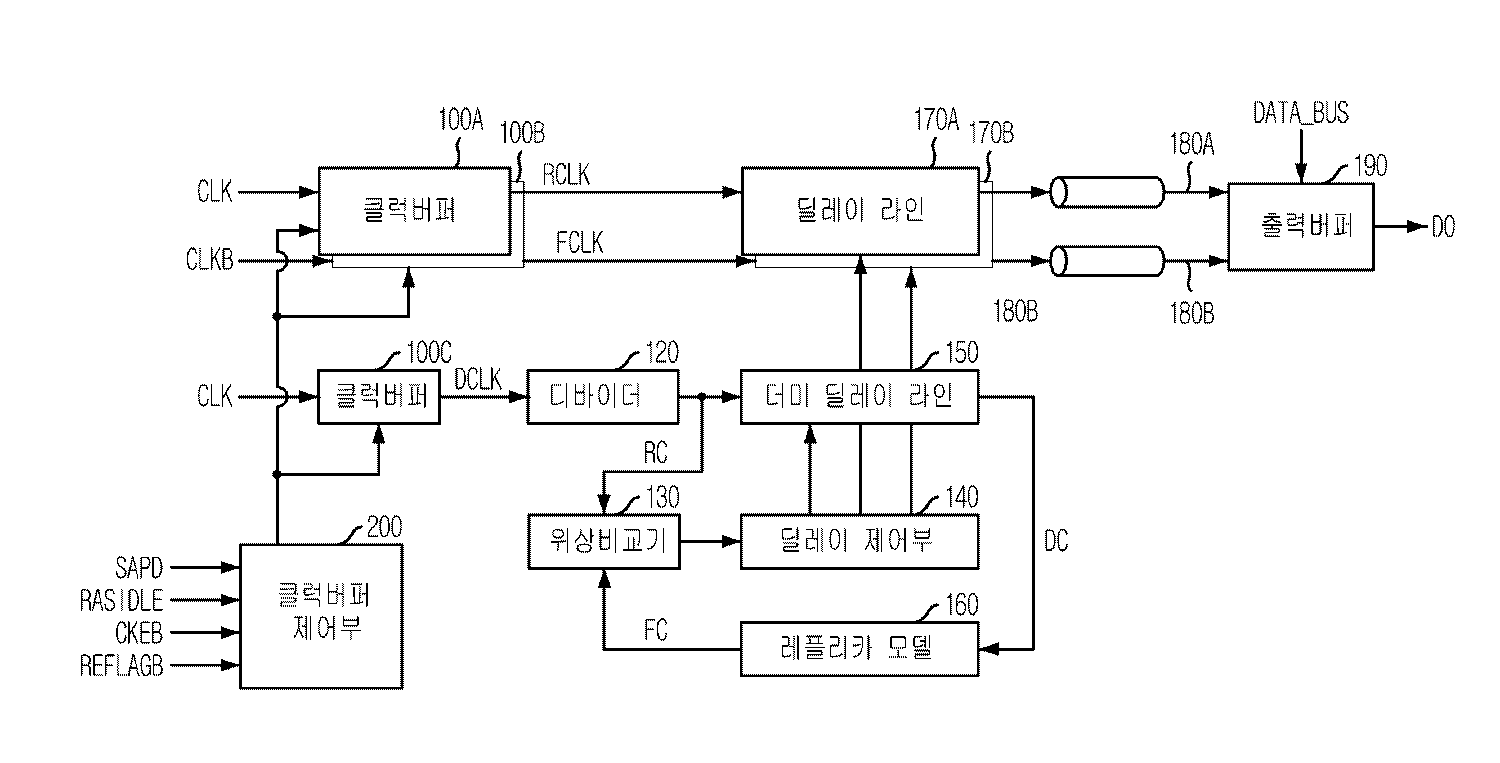
도1는 본 발명의 바람직한 실시예에 따른 반도체 장치를 나타내는 블럭도.1 is a block diagram showing a semiconductor device according to a preferred embodiment of the present invention.
도2a와 도2b는 도1에 도시된 반도체 장치의 동작모드를 나타내는 테이블도.2A and 2B are table diagrams showing an operation mode of the semiconductor device shown in FIG.
도3는 도1에 도시된 클럭버퍼 제어부의 제1 실시예에 따른 회로도.3 is a circuit diagram according to a first embodiment of the clock buffer control unit shown in FIG.
도4a와 도4b는 도3의 클럭버퍼 제어부의 동작을 나타내는 파형도.4A and 4B are waveform diagrams showing the operation of the clock buffer controller of FIG.
도5는 도1에 도시된 클럭버퍼 제어부의 제2 실시예에 따른 회로도.5 is a circuit diagram according to a second embodiment of the clock buffer control unit shown in FIG.
도6a와 도6b는 도3의 클럭버퍼 제어부의 동작을 나타내는 파형도.6A and 6B are waveform diagrams showing the operation of the clock buffer controller of FIG.
도7은 도1의 반도체 장치의 SREM 모드를 나타내는 파형도.7 is a waveform diagram showing an SREM mode of the semiconductor device of FIG.
* 도면의 주요부분에 대한 부호의 설명 *Explanation of symbols on the main parts of the drawings
200 : 클럭버퍼 제어부200: clock buffer control unit
110A,110B,110C : 클럭버퍼 120 : 디바이더110A, 110B, 110C: Clock buffer 120: Divider
130 : 위상비교기 140 : 딜레이 제어부130: phase comparator 140: delay control unit
150 : 더미 딜레이라인 160 : 레플리카 모델150: dummy delay line 160: replica model
170A, 170B : 딜레이 라인 180A,180B : 클럭신호 전달라인170A, 170B:
190 : 출력버퍼190: output buffer
본 발명은 반도체 집적회로에 관한 것으로, 특히 반도체 메모리 장치의 지연고정동작을 제어하기 위한 회로에 관한 것이다.BACKGROUND OF THE
복수의 반도체 장치들로 구성된 시스템에서 반도체 메모리 장치는 데이터를 저장하기 위한 것이다. 데이터 처리 장치, 예를 들면 중앙처리장치(CPU)등에서 데이터를 요구하게 되면 반도체 메모리 장치는 데이터 요구 장치로부터 입력된 어드레스에 대응하는 데이터를 출력하거나, 그 어드레스에 대응하는 위치에 데이터 요구 장치로 부터 입력되는 데이터를 저장한다.In a system composed of a plurality of semiconductor devices, the semiconductor memory device is for storing data. When data is requested from a data processing device, such as a central processing unit (CPU), the semiconductor memory device outputs data corresponding to an address input from the data requesting device, or from a data requesting device at a position corresponding to the address. Save the input data.
반도체 장치들로 구성된 시스템의 동작속도가 빨라지고, 반도체 집적회로에 관한 기술이 발달하면서, 반도체 메모리 장치는 보다 빠른 속도로 데이터를 출력하거나 저장하도록 요구되어 왔다. 고속으로 데이터를 입출력시키기 위해서, 시스템 클럭을 입력받은 다음, 입력받는 시스템 클럭에 동기되어 데이터를 입/출력시킬 수 있는 동기식 메모리 장치가 개발되었다. 동기식 메모리 장치로도 요구되는 데이터 입출력속도를 만족시키기가 충분하지 않아서, 시스템 클럭의 라이징 에지와 폴링에지에 각각 데이터가 입/출력되는 DDR(Double Data Rate) 동기식 메모리 장치가 개발되었다.As the operating speed of a system composed of semiconductor devices becomes faster and the technology related to semiconductor integrated circuits develops, semiconductor memory devices have been required to output or store data at higher speeds. In order to input and output data at high speed, a synchronous memory device capable of inputting / outputting data in synchronization with an input system clock and then receiving a system clock has been developed. Since even the synchronous memory device does not satisfy the required data input / output speed, a DDR (Double Data Rate) synchronous memory device has been developed in which data is input and output at the rising edge and the falling edge of the system clock, respectively.
DDR 동기식 메모리 장치는 시스템 클럭의 라이징 에지와 폴링에지에 각각 데이터를 입출력시켜야 하기 때문에 시스템 클럭의 한 주기 안에서 2개의 데이터를 처리해야 한다. 즉, DDR 동시기 메모리 장치는 클럭신호의 라이징 에지 및 폴링에지에 각각 데이터를 출력하거나 입력받아 저장해야만 하는 것이다. 특히 DDR 메모리 장치가 데이터를 출력하는 타이밍은 시스템 클럭의 라이징 에지 또는 폴링에지에 정확하게 동기시켜 출력시켜야 한다. 따라서 DDR 메모리 장치의 출력버퍼는 입력된 시스템 클럭의 라이징 에지와 폴링에지에 동기시켜 데이터를 출력시키게 된다.DDR synchronous memory devices must process two data in one cycle of the system clock because the data must be input and output to the rising edge and the falling edge of the system clock, respectively. In other words, the DDR synchronizer memory device must output or receive data at the rising edge and the falling edge of the clock signal, respectively. In particular, the timing at which the DDR memory device outputs data must be accurately synchronized to the rising edge or falling edge of the system clock. Therefore, the output buffer of the DDR memory device outputs data in synchronization with the rising edge and the falling edge of the input system clock.
그러나, 메모리 장치에 입력된 시스템 클럭은 내부의 입력버퍼, 클럭신호 전송라인등에 의해 필연적으로 지연시간을 가지고 출력버퍼에 도달하게 된다. 따라서 이미 지연시간을 가지고 전달된 시스템 클럭에 동기시켜 데이터를 출력하더라도, 반도체 메모리 장치의 출력데이터를 전달받는 외부의 장치는 시스템 클럭의 라이징 에지와 폴링 에지와는 맞지 않는 타이밍에서 데이터를 전달받게 된다.However, the system clock input to the memory device inevitably reaches the output buffer with a delay time by an internal input buffer, a clock signal transmission line, and the like. Therefore, even if the data is output in synchronization with the system clock that has already been delayed, the external device receiving the output data of the semiconductor memory device receives the data at timings that do not match the rising and falling edges of the system clock. .
이를 해결하기 위해, 반도체 메모리 장치는 클럭신호의 지연을 고정시키는 회로를 구비하고 있다. 지연고정회로는 시스템 클럭이 메모리 장치에 입력되어 출력버퍼로 전달될 때까지 메모리 장치의 내부 회로에 의해 지연되는 값을 보상하기 위한 회로이다. 지연고정회로는 시스템 클럭이 반도체 메모리 장치의 클럭 입력버퍼 및 클럭신호 전송라인등에 의해 지연되는 시간을 찾아내고, 찾아낸 값에 대응하여 시스템 클럭을 지연시켜 출력버퍼로 출력한다. 즉, 지연고정회로에 의해서 메모리 장치에 입력된 시스템 클럭은 지연값이 일정한 상태로 유지한 채로 출력버퍼로 전달되는 것이다. 이 때의 클럭을 지연고정된 클럭이라고 한다. 출력버퍼는 지연고정된 클럭에 동기시켜 데이터를 출력하고, 외부에서는 시스템 클럭에 정확하게 동 기되어 데이터가 출력되는 것으로 판단하게 되는 것이다.In order to solve this problem, the semiconductor memory device includes a circuit for fixing a delay of a clock signal. The delay lock circuit is a circuit for compensating for a value delayed by an internal circuit of the memory device until the system clock is input to the memory device and transferred to the output buffer. The delay lock circuit finds a time at which the system clock is delayed by the clock input buffer and the clock signal transmission line of the semiconductor memory device, and delays the system clock corresponding to the found value to output the output buffer. That is, the system clock input to the memory device by the delay lock circuit is transmitted to the output buffer with the delay value kept constant. The clock at this time is called a delay locked clock. The output buffer outputs data in synchronization with a delayed clock and externally judges that the data is correctly synchronized with the system clock.
실제동작은 데이터가 출력되어야 하는 시점보다 한 주기 앞 선 시점에서 지연고정회로에서 출력되는 지연고정클럭이 출력버퍼에 전달되고, 전달된 지연고정클럭에 동기시켜 데이터를 출력하게 된다. 따라서 시스템 클럭이 메모리 장치의 내부회로에 의해 지연되는 만큼보다 더 빠르게 데이터를 출력시키는 것이 되는 것이다. 이렇게 함으로서, 메모리 장치의 외부에서는 메모리 장치에 입력된 시스템 클럭의 라이징 에지와 폴링에지에 각각 정확하게 동기되어 데이터가 출력되는 것처럼 보이는 것이다. 결국 지연고정회로는 데이터를 얼마만큼 더 빨리 출력시켜야 메모리 장치의 내부에서 시스템 클럭의 지연값을 보상할 수 있는지 찾아내는 것이다. In the actual operation, the delay lock clock output from the delay lock circuit is transferred to the output buffer at a point before the data should be output, and the data is output in synchronization with the delay lock clock. Therefore, the system clock outputs data faster than the delay of the internal circuit of the memory device. By doing so, it appears that data is output from the memory device in synchronization with the rising edge and the falling edge of the system clock input to the memory device. After all, the delay lock circuit finds out how much faster data must be output to compensate for the delay of the system clock inside the memory device.
한편, DDR 메모리 장치에 구비되는 지연고정회로는 시스템 클럭의 천이 타이밍과 내부회로에 의해 지연되는 값을 계속 비교해야 하기 때문에 지연고정이 될 때까지는 계속해서 동작해야 하는 회로다. 따라서 지연고정회로는 다른 회로들보다 많은 전류를 소모하게 된다.On the other hand, the delay lock circuit provided in the DDR memory device is a circuit that must continue to operate until the delay lock because it is necessary to continuously compare the transition timing of the system clock and the value delayed by the internal circuit. Therefore, the delay lock circuit consumes more current than other circuits.
DDR 메모리 장치는 소비전류를 줄이기 위해 지연고정회로를 계속 동작시키는 것이 아니라, 파워다운모드등 실질적으로 메모리 장치가 동작하지 않는 중에서는 지연고정회로를 동작하지 않게 제어한다.The DDR memory device does not continuously operate the delay lock circuit to reduce the current consumption, but controls the delay lock circuit not to operate while the memory device is not actually operated, such as a power-down mode.
DDR 메모리 장치의 성능이 계속 개선되면서, 다양한 동작모드가 필요하게 되었다. 예를 들면, 파워다운 모드도 프리차지 파워다운모드, 액티브 파워다운모드등의 동작모드가 생기게 된 것이다. 따라서 DDR 메모리장치에는 각각의 동작모드에 적절히 대응하는 제어회로가 필요하게 되었다. 지연고정회로에 대한 동작제어도 각 각의 제어상황에 맞도록 적절하게 지연고정회로를 동작시킬 것인지 동작시키지 않을 것인지에 대한 동작을 뒷받침할 수 있는 제어회로가 필요하게 되었다.As the performance of DDR memory devices continues to improve, various modes of operation are required. For example, the power down mode also has an operation mode such as a precharge power down mode and an active power down mode. Therefore, the DDR memory device requires a control circuit appropriately corresponding to each operation mode. The operation control for the delay lock circuit also needs a control circuit that can support the operation of operating or not operating the delay lock circuit appropriately for each control situation.
본 발명의 메모리 장치의 다양한 동작모드에서 지연고정회로를 적절하게 제어할 수 있는 제어회로를 구비한 반도체 메모리 장치를 제공하는 것을 목적으로 한다.An object of the present invention is to provide a semiconductor memory device having a control circuit capable of appropriately controlling a delay lock circuit in various operation modes of the memory device of the present invention.
본 발명은 외부로 부터 시스템 클럭을 입력받아 내부클럭으로 출력하는 클럭버퍼; 데이터의 출력타이밍이 상기 시스템 클럭에 동기될 수 있도록, 상기 내부클럭의 지연을 제어하기 위한 지연고정회로부; 상기 지연고정된 내부클럭에 동기시켜 데이터를 출력시키기 위한 데이터 출려버퍼; 및 상기 클럭버퍼의 온/오프를 제어하기 위한 인에이블 신호를 출력하되, 동일한 논리 레벨의 입력신호들에 대응하여, 이전 동작의 상태에 따라 상기 인에이블 신호의 서로 다른 논리레벨을 얻기 위하여 래치를 포함하는 클럭버퍼 제어부를 구비하는 반도체 메모리 장치를 제공한다.The present invention provides a clock buffer for receiving a system clock from the outside and outputting the internal clock; A delay lock circuit for controlling a delay of the internal clock so that output timing of data can be synchronized with the system clock; A data output buffer for outputting data in synchronization with the delayed internal clock; And outputting an enable signal for controlling on / off of the clock buffer, corresponding to input signals having the same logic level, and latching to obtain different logic levels of the enable signal according to a state of a previous operation. A semiconductor memory device including a clock buffer control unit is provided.
또한 본 발명은 빠른 프리차지 파워다운 모드와 셀프 리프레쉬 에뮬레이션 모드를 갖는 반도체 메모리장치에 있어서, 외부로 부터 시스템 클럭을 입력받아 내부클럭으로 출력하는 클럭버퍼; 데이터의 출력타이밍이 상기 시스템 클럭에 동기될 수 있도록, 상기 내부클럭의 지연을 제어하기 위한 지연고정회로부; 및 상기 빠른 프리차지 파워다운 모드와 상기 셀프 리프레쉬 에뮬레이션 모드에 의한 파워 다운 모드에서 각각 동일한 논리 레벨을 가지는 제어신호들을 인가받되, 상기 빠른 프리차지 파워다운 모드시에는 상기 클럭버퍼를 온시키고 상기 셀프 리프레쉬 에뮬레이션 모드의 파워 다운 모드시에는 상기 클럭버퍼를 오프시키는 인에이블신호를 생성하기 위하여 래치를 포함하는 클럭버퍼 제어부를 구비하는 반도체 메모리장치를 제공한다.The present invention also provides a semiconductor memory device having a fast precharge power down mode and a self refresh emulation mode, comprising: a clock buffer which receives a system clock from an external source and outputs it to an internal clock; A delay lock circuit for controlling a delay of the internal clock so that output timing of data can be synchronized with the system clock; And control signals having the same logic level in the fast precharge power-down mode and the power down mode by the self-refresh emulation mode. In the fast precharge power-down mode, the clock buffer is turned on and the self refresh is performed. In the power down mode of the emulation mode, a semiconductor memory device including a clock buffer control unit including a latch is provided to generate an enable signal for turning off the clock buffer.
또한 본 발명은 커맨드 디코더 및 모드레지스터; 클럭버퍼를 구비하는 지연고정회로; 및 상기 클럭버퍼의 온/오프를 제어하여 상기 지연고정회로에서 출력되는 지연고정된 클럭신호의 업데이트 여부를 결정하기 위한 인에이블 신호를 출력하는 클럭버퍼 제어부를 구비하고, 상기 클럭버퍼 제어부는 상기 커맨드디코더 및 상기 모드레지스터로부터 동일 논리 레벨의 입력신호들을 인가받더라도 이전의 메모리 동작에 따라 서로 다른 파워다운모드에서 서로 다른 논리 레벨의 상기 인에이블신호를 제공하기 위하여 래치를 구비하는 것을 특징으로 하는 반도체 메모리장치를 제공한다.The present invention also provides a command decoder and a mode register; A delay lock circuit having a clock buffer; And a clock buffer controller for controlling on / off of the clock buffer and outputting an enable signal for determining whether to update a delayed clock signal output from the delay lock circuit. And a latch provided to provide the enable signals of different logic levels in different power-down modes according to a previous memory operation even when input signals of the same logic level are applied from the decoder and the mode register. Provide the device.
이하, 본 발명이 속하는 기술분야에서 통상의 지식을 가진 자가 본 발명의 기술적 사상을 용이하게 실시할 수 있을 정도로 상세히 설명하기 위하여, 본 발명의 가장 바람직한 실시예를 첨부된 도면을 참조하여 설명하기로 한다.DETAILED DESCRIPTION Hereinafter, exemplary embodiments of the present invention will be described with reference to the accompanying drawings so that those skilled in the art may easily implement the technical idea of the present invention. do.
도1은 본 발명의 바람직한 실시예에 따른 반도체 메모리 장치를 나타내는 블럭도이다.1 is a block diagram illustrating a semiconductor memory device according to a preferred embodiment of the present invention.
도1을 참조하여 살펴보면, 본 실시예에 따른 반도체 메모리 장치는 클럭버퍼(110A, 110B, 110C)와, 디바이더(120)와, 위상비교기(130)와, 딜레이제어부(140)와, 더미 딜레이라인(150)과, 레플리카 모델(160)과, 딜레이라인(170A,170B)와, 출력버퍼(190)와, 클럭버퍼(110A, 110B, 110C)를 제어하기 위한 클럭버퍼 제어부(200)를 구비한다. 지연고정회로는 다양한 회로를 구비할 수 있는데, 여기서는 디바이더(120)와, 위상비교기(130)와, 딜레이제어부(140)와, 더미 딜레이라인(150)과, 레플리카 모델(160)과, 딜레이라인(170A,170B)등의 회로가 지연고정회로의 회로를 이루게 된다. 또한, 딜레이라인(170A,170B)과 출력버퍼(190)의 사이에는 클럭신호 전송라인(180A,180B)이 배치된다.Referring to FIG. 1, the semiconductor memory device according to the present embodiment includes a clock buffer 110A, 110B, and 110C, a
복수의 클럭버퍼(110A, 110B, 110C)는 외부에서 입력되는 시스템 클럭(CLK)을 입력받아 복수의 내부 클럭(RCLK,RCLK,DCLK)을 각각 출력하는 장치이다. 클럭버퍼(110A,110B)는 각각 시스템 클럭(CLK)과 그 반전된 시스템 클럭(CLKB)의 입력을 위한 버퍼이다. 클럭버퍼(110C)는 시스템 클럭을 입력받기 위한 클럭버퍼이며, 지연고정회로의 지연고정동작을 위해 별도로 배치되는 버퍼이다.The plurality of clock buffers 110A, 110B, and 110C receive a system clock CLK input from the outside and output a plurality of internal clocks RCLK, RCLK, and DCLK, respectively. The clock buffers 110A and 110B are buffers for inputting the system clock CLK and the inverted system clock CLKB, respectively. The clock buffer 110C is a clock buffer for receiving a system clock and is a buffer disposed separately for the delay lock operation of the delay lock circuit.
디바이더(120)는 내부클럭(DCLK)을 소정값으로 분주한 기준클럭(RC)을 더미 딜레이라인(150)로 출력한다. 디바이더(120)는 내부클럭(DCLK)의 주파수를 1/N(N은 양수, 보통 8 내지 4의 값을 가진다.)로 분주하게 된다. 여기서 디바이더(120)가 내부클럭(DCLK)을 분주하여 출려하는 이유는 지연고정동작의 횟수를 최대한 줄이기 위해서이다. 지연고정회로의 지연고정동작은 디바이더(120)에서 출력된 분주된 기준클럭(RC)의 천이시점마다 이루어지게 된다. 따라서 분주된 클럭을 이용해서 지연고정동작을 수행하게 되면, 내부클럭(DCLK)을 사용하여 지연고정동작을 수행할 때 보다, 지연고정동작에 소모되는 전류가 줄어들게 되는 것이다.The
위상비교기(130)는 디바이더(120)에서 출력되는 기준클럭(RC)와 피드백 클럭(FC)의 위상을 비교한다.The
딜레이 제어부(140)는 위상비교기(130)에서 제공되는 기준클럭(RC)와 피드백 클럭(FC)의 위상을 비교결과에 응답하여 더미 딜레이라인(150)과 딜레이라인(170A,170B)에서 지연되는 값이 조절되도록 제어한다.The
더미 딜레이라인(150)은 딜레이 제어부(140)의 제어에 대응하는 지연값만큼 디바이더의 출력인 기준클럭(RC)을 지연시켜 딜레이된 클럭(DC)을 레프리카 모델(160)로 출력한다.The
레플리카 모델(160)은 시스템 클럭(CLK)이 입력되어 출력버퍼로 전달될 때까지의 지연값을 모델링하기 위한 것이다. 특히, 클럭버퍼(110A,110B)에 의한 지연시간과 전송라인(180A,180B)에 의해 시스템 클럭의 전달이 지연되는 정도를 모델링하게 된다. 레플리카 모델(160)은 모델링에 의해 정해진 지연값 만큼 더미 딜레이 라인(150)에서 출력되는 딜레이된 클럭(DC)을 지연시켜 피드백 클럭(FC)로 출력하게 된다. 레플리카 모델(160)에서 모델링하는 지연값은 그 정확성에 따라서 지연고정회로에서 지연고정된 클럭의 정확성이 결정되는 중요한 값이다. 따라서 레플리카 모델(160)은 모델링하는 회로와 똑같은 회로를 구비하거나, 모델링할 대상 회로를 일정 비율로 줄인 회로를 구비하게 된다.The
딜레이 라인(170A,170B)는 각각 내부클럭(RCLK,FCLK)를 입력받아 딜레이제어부(140)의 제어에 대응하는 지연값만큼 지연시켜 출력한다. 여기서 출력된 신호는 전송라인(180A,180B)을 통해 출력버퍼(190)으로 출력된다.The
위상비교기(130)는 입력되는 두 신호(RC,FC)의 위상을 비교하여 어느 신호가 위상이 앞선 신호인지를 딜레이 제어부(140)로 출력한다. 딜레이 제어부(140)는 위상비교기(130)에서 출력되는 신호에 응다하여 딜레이 라인(170A,170B)과 더미 딜레이 라인(150)의 지연값을 조정하게 된다. 구체적으로 딜레이 라인(170A,170B)과 더미 딜레이 라인(150)의 지연값을 증가시키던지 감소시키던지 하게 된다.The
위상비교기(130)는 입력되는 두 신호(RC,FC)의 위상이 같게 되면, 딜레이 제어부(140)는 딜레이 라인(170A,170B)과 더미 딜레이 라인(150)의 지연값을 변화시키지 않고 고정되도록 한다.When the
출력버퍼(190)는 전송라인(180A,180B)에 의해 전달된 내부클럭(RCLK,FCLK)에 응답하여 메모리 코어영역으로 부터 전달된 데이터(DATA_BUS)를 외부로 출력하게 된다.The
한편, 클럭버퍼 제어부(200)는 제어신호(SAPD,RASIDLE,CKEB,REFLAGB)를 입력받아 클럭버퍼(110A,110B,110C)를 활성화시키기 위한 인에이블 신호(CB_ENB)를 출력한다. 클럭버퍼(110A,110B,110C)는 인에이블 신호(CB_ENB)가 활성화되면 시스템 클럭(CLK,CLKB)을 입력받아 내부클럭(RCLK,FCLK,DCLK)을 출력하게 된다.The
클럭버퍼(110A,110B,110C)에서 내부클럭(RCLK,FCLK,DCLK)을 출력하지 않으면, 지연고정동작을 진행되지 않는다. 따라서 클럭버퍼 제어부(200)은 메모리 장치가 동작하지 않을 때는 불필요한 전류소모를 막기 위해서 인에이블 신호(CB_ENB)를 비활성화시키고, 메모리 장치가 동작하는 동안만 인에이블 신호(CB_ENB)를 활성화 시켜 출력하게 된다. If the internal clocks RCLK, FCLK, and DCLK are not output from the clock buffers 110A, 110B, and 110C, the delay lock operation does not proceed. Therefore, when the memory device is not operating, the
보다 효과적으로 데이터를 입/출력시키기 위해, DDR 메모리 장치는 특정한 스펙으로 동작하도록 제조되는데, 그 단계별로 DDR,DDR2,DDR3으로 나누어진다.In order to input and output data more effectively, DDR memory devices are manufactured to operate to specific specifications, which are divided into DDR, DDR2, and DDR3 stages.
도2a는 DDR2 스펙을 지원하는 반도체 메모리 장치의 동작모드 테이블이며, 도2b는 DDR3 스펙을 지원하는 반도체 메모리 장치의 동작모드 테이블이다.2A is an operation mode table of a semiconductor memory device supporting the DDR2 specification, and FIG. 2B is an operation mode table of the semiconductor memory device supporting the DDR3 specification.
여기서 제어신호(SAPD)는 슬로우 파워다운모드에서는 로직 하이레벨, 액티브 파워다운모드에서는 로직 로우레벨을 유지하는 신호이다. 클럭인에이블 신호(CKEB)는 메모리 장치가 동작중에는 시스템 클럭을 메모리 장치의 내부로 전달하고, 메모리 장치가 동작중이 아닐때에는 시스템 클럭을 메모리 장치의 내부로 전달을 막는 신호이다. 제어신호(REFLAGB)는 메모리 장치가 리프레쉬동작중일 때에는 로직 로우레벨로 인에이블되는 신호이다. 제어신호(RASIDLE)는 아이들(idle)모드에서 로직 하이레벨을 유지하고, 액티브모드(Active)에서 로직 로우레벨을 유지하는 신호이다. The control signal SAPD maintains a logic high level in the slow power down mode and a logic low level in the active power down mode. The clock enable signal CKEB is a signal that prevents the system clock from being transmitted to the inside of the memory device when the memory device is in operation, and prevents the system clock from being transferred into the memory device when the memory device is not in operation. The control signal REFLAGB is a signal that is enabled at a logic low level when the memory device is in the refresh operation. The control signal RASIDLE is a signal that maintains a logic high level in an idle mode and maintains a logic low level in an active mode.
먼저, DDR2 스펙을 지원하는 메모리 장치는 프리차지 파워다운 모드(Precharge power donw) 즉, IDD2P 상황에서는 모드 레지스터 세트(MRS)에서 출력되는 신호인 제어신호(SAPD)의 로직 하이레벨 또는 로직 로우레벨에 상관없이 지연고정 동작의 업데이트가 되지 않는다. 즉, 인에이블 신호(CB_ENB)는 로직 하이레벨이 되어야 하는 것이다.First, a memory device that supports the DDR2 specification has a precharge power down mode, that is, a logic high level or a logic low level of a control signal SAPD, which is a signal output from a mode register set (MRS) in an IDD2P situation. Regardless, the delay lock operation is not updated. That is, the enable signal CB_ENB should be at a logic high level.
삭제delete
삭제delete
삭제delete
한편, DDR3 스펙을 지원하는 메모리 장치는 IDD2P 상황에서는 제어신호(SAPD)가 하이레벨일 때는 슬로우 프리차지 파워다운 모드(slow precharge power down mode)로서 지연고정회로의 업데이트가 되지 않고, 제어신호(SAPD)라 로우레벨일 때는 패스트 프리차지 파워다운 모드(fast precharge power down mode)로서 지연고정회로의 업데이트가 된다. 지연고정 동작의 업데이트가 된다는 것은 계속 지연고정동작을 진행되는 것이고, 지연고정 동작의 업데이트가 되지 않는다는 것은 지연고정동작을 진행하지 않는것을 나타낸다. 즉, 업데이트가 된다는 것은 위상비교기가 계속해서 동작을 하여 지연고정되어야 할 클럭을 계속 추적한다는 것을 말하고, 업데이트가 되지 않는다는 것은 이전 지연고정된 상태를 유지하고 있고, 유지된 정보에 의한 클럭이 출력되는 것을 말한다. 파워다운 모드을 탈출한 직후에 업데이트가 되지 않는다면 이전 지연고정된 클럭이 바로 출력버퍼로 제공된다.On the other hand, the memory device supporting the DDR3 specification is a slow precharge power down mode when the control signal SAPD is at a high level in the IDD2P situation, and the delay lock circuit is not updated, and the control signal SAPD is not used. At the low level, a fast precharge power down mode is used to update the delay lock circuit. Updating the delayed fixed operation means continuing the delayed fixed operation, and not updating the delayed fixed operation indicates that the delayed fixed operation is not performed. In other words, the update means that the phase comparator keeps track of the clock to be delayed and the update keeps the previous delayed state, and the clock by the retained information is output. Say that. If the update does not occur immediately after exiting the power-down mode, the previous delayed clock is provided directly to the output buffer.
또한 DDR2 스펙을 지원하는 메모리 장치는 액티브 파워 다운모드인 IDD3P 상황일 때는 제어신호(SAPD)가 하이레벨(슬로우 프리차지 파워다운 모드인 경우) 또는 로우레벨(패스트 프리차지 파워다운 모드인 경우)에 따라 지연고정회로의 업데이트 여부를 결정하게 된다. 반면에 DRR3 스펙을 지원하는 메모리 장치에서는 제어신호(SAPD)가 하이레벨 또는 로우레벨에 상관없이, 즉 슬로우 프리차지 파워다운 모드 또는 패스트 프리차지 파워다운 모드에 상관없이 액티브 파워상황에서는 지연고정동작의 업데이트가 되어야 한다. 즉 인에이블 신호(CB_ENB)는 로직 로우레벨이 되어야 하는 것이다.In addition, memory devices that support the DDR2 specification have a control signal (SAPD) at high level (in slow precharge power down mode) or low level (in fast precharge power down mode) when IDD3P is active power down mode. Accordingly, it is determined whether or not the delay lock circuit is updated. On the other hand, in memory devices that support the DRR3 specification, whether the control signal SAPD is high or low level, that is, regardless of the slow precharge power down mode or the fast precharge power down mode, the delay lock operation may be performed in an active power situation. It should be updated. That is, the enable signal CB_ENB should be at a logic low level.
삭제delete
또한, DDR2 스펙을 지원하는 메모리 장치와 DDR3 스펙을 지원하는 메모리 장치는 모두 셀프 리프레쉬 에뮬레이션 모드(Self Refresh emulation mode,SREM)를 지원해야 한다. 이 때 DDR3 스펙을 지원하는 메모리 장치는 제어신호(SAPD)가 로우레벨일 때 IDD2PF 동작모드와 셀프 리프레쉬 에뮬레이션 모드(SREM) 동작 진행후 액티브 파워다운 모드로 진입하는 제어신호의 조합이 같다. 하지만 인에이블 신호(CB_ENB)는 IDD2PF(fast) 상황일 때는 로우레벨을 유지하여 지연고정동작의 업데이트가 일어나도록 해야 한다. 셀프 리프레쉬 에뮬레이션 모드(SREM) 동작 진행후 액티브 파워다운모드로 진입하는 상황일 때는 제어신호(CB_ENB)가 로직 하이레벨이 되어 지연고정동작의 업데이트가 일어나지 않도록 해야 한다. 지연고정동작의 업데이트가 일어나지 않아야 지연고정회로에 의한 전류소모를 줄일 수 있는 것이다.In addition, both memory devices that support the DDR2 specification and memory devices that support the DDR3 specification must support Self Refresh emulation mode (SREM). In this case, the memory device supporting the DDR3 specification has the same combination of the control signal entering the active power-down mode after the IDD2PF operation mode and the self refresh emulation mode (SREM) operation when the control signal SAPD is low. However, the enable signal CB_ENB should be kept at the low level in the IDD2PF (fast) state to update the delay lock operation. In the case of entering the active power down mode after the SREM operation, the control signal CB_ENB becomes the logic high level so that the update of the delay lock operation does not occur. If the delay lock operation is not updated, the current consumption by the delay lock circuit can be reduced.
도3는 도1에 도시된 클럭버퍼 제어부의 제1 실시예에 따른 회로도이다.FIG. 3 is a circuit diagram according to a first embodiment of the clock buffer controller shown in FIG.
도2a의 동작모드에 대한 테이블대로 동작시키기 위한 클럭버퍼 제어부의 내부 회로도이다. Fig. 2A is an internal circuit diagram of the clock buffer controller for operating according to the table for the operation mode of Fig. 2A.
도3을 참조하여 살펴보면, 제어신호(SAPD,REFLAGB)와 클럭인에이블 신호(CKEB)를 입력받는 낸드게이트(ND1)와, 제어신호(REFLAGB,RASIDLE)와 클럭인에이 블 신호(CKEB)를 입력받는 낸드게이트(ND2)와 낸드게이트(ND1,ND2)의 출력을 입력받아 인에이블 신호(CB_ENB)를 출력하기 위한 낸드게이트(ND3)를 구비한다.Referring to FIG. 3, the NAND gate ND1 receiving the control signals SAPD and REFLAGB and the clock enable signal CKEB, and the control signals REFLAGB and RASIDLE and the clock enable signal CKEB are inputted. And a NAND gate ND3 for receiving the outputs of the NAND gates ND2 and the NAND gates ND1 and ND2 and outputting the enable signal CB_ENB.
또한, 도4a와 도4b는 도3의 클럭버퍼 제어부의 동작을 나타내는 파형도이다.4A and 4B are waveform diagrams illustrating the operation of the clock buffer controller of FIG.
도4a에는 제어신호(SAPD)가 하이레벨인 경우, 클럭인에이블신호(CKEB)와 제어신호(RASIDLE,REFLAGB)의 상태에 따라 클럭버퍼 제어부(200)에서 출력되는 인에이블 신호(CB_ENB)의 인에이블 여부에 대한 파형이 도시되어 있다.In FIG. 4A, when the control signal SAPD is at a high level, the enable signal CB_ENB output from the
또한, 도4b에는 제어신호(SAPD)가 로우레벨인 경우, 클럭인에이블신호(CKEB)와 제어신호(RASIDLE,REFLAGB)의 상태에 따라 클럭버퍼 제어부(200)에서 출력되는 인에이블 신호(CB_ENB)의 인에이블 여부에 대한 파형이 도시되어 있다.In addition, in FIG. 4B, when the control signal SAPD is at the low level, the enable signal CB_ENB output from the
도5는 도1에 도시된 클럭버퍼 제어부의 제2 실시예에 따른 회로도이다.FIG. 5 is a circuit diagram according to a second embodiment of the clock buffer controller shown in FIG.
도5에 도시된 바와 같이, 제2 실시예에 따른 클럭버퍼 제어부(200)는 클럭버퍼(110A,110B,110C)의 온/오프를 제어하기 위한 인에이블 신호(CB_ENB)를 출력하되, 동일한 논리 레벨의 제어신호(CKEB, REFLAGB)들에 대응하여, 이전 동작의 상태에 따라 인에이블 신호(CB_ENB)의 서로 다른 논리레벨을 얻기 위하여 래치(LA)를 구비한다.As shown in FIG. 5, the
클럭버퍼 제어부(200)는 클럭인에이블 신호(CKE)를 입력받아 내부 인에이블 신호를 제공하기 위한 제1 로직회로부(210)와, 클럭인에이블 신호(CKE)와 리프레쉬 구간동안 활성화상태를 유지하는 리프레쉬 제어신호(REFLAGB)를 입력받아, 구비된 래치(LA)를 이용하여 동작모드의 대응하는 레벨을 가지는 동작모드 선택신호(Q)를 출력하기 위한 제2 로직회로부(220)와, 인에이블 신호에 활성화상태에 응답하여 동작모드 선택신호(Q)를 인에이블 신호(CB_ENB)로 출력하기 위한 제3 로직회로부(230)를 구비한다.The
제1 로직회로부(210)는 클럭인에이블 신호(CKEB)와 아이들 모드(IDLE)에서 활성화되는 아이들모드 제어신호(RASIDLE)와 셀프 리프레쉬 에뮬레이션 모드(SREM)에 활성화되는 셀프 제어신호(SAPD)의 로직 논리곱을 수행하기 위한 제1 논리곱부를 구비한다. 제1 논리곱부는 클럭인에이블 신호(CKEB)와 아이들모드 제어신호(RASIDLE)와 셀프 제어신호(SAPD)를 입력받는 낸드 게이트(NA4)를 구비한다.The
제2 로직회로부(220)는 클럭인에이블 신호(CLEB)와 리프레쉬 제어신호(REFLAGB)의 로직 논리곱을 수행하기 위한 제2 논리곱부(221)와, 클럭인에이블 신호(CKEB)와 반전된 리프레쉬 제어신호(REFLAGB)의 로직 논리곱을 수행하기 위한 제3 논리곱부(222)와, 반전된 클럭인에이블 신호(CKEB)와 리프레쉬 제어신호(REFLAGB)의 로직 논리곱을 수행하기 위한 제4 논리곱부(223)와, 제2 논리곱부(221)의 출력과 제3 논리곱부(223)의 출력을 각각 일측으로 입력받으며, 각각의 출력이 서로의 타측 입력으로 입력되어 래치(LA)를 이루는 제5 및 제6 논리곱부(224,225)와, 제2 논리곱부(221)의 출력과 제5 논리곱부(224)의 출력의 로직 논리곱 수행을 위한 제7 논리곱부(226)를 구비한다.The
제2 논리곱부(221)는 리프레쉬 제어신호(REFLAGB)와 클럭인에이블 신호(CKEB)를 입력받는 낸드게이트(ND5)와, 낸드게이트(ND2)의 출력을 반전하여 제7 논리곱부(226)로 출력하기 위한 인버터(I1)를 구비한다.The second
제3 논리곱부(222)는 리프레쉬 제어신호(REFLAGB)를 반전하여 전달하기 위한 인버터(I2)와, 클럭인에이블 신호(CKEB)와 인버터(I2)의 출력을 입력받는 낸드게이트(ND6)를 구비한다.The third
제4 논리곱부(223)는 클럭인에이블 신호(CKEB)를 반전하여 전달하기 위한 인버터(I3)와, 리프레쉬 제어신호(REFLAGB)와 인버터(I3)의 출력을 입력받는 낸드게이트(ND7)를 구비한다.The fourth
제5 논리곱부(224)는 제6 논리곱부(225)의 출력과 낸드게이트(ND6)의 출력을 입력받는 낸드게이트(ND8)를 구비한다.The fifth
제6 논리곱부(225)는 제5 논리곱부(224)의 출력과 낸드게이트(ND7)의 출력을 입력받는 낸드게이트(ND9)를 구비한다.The sixth
제7 논리곱부(226)는 인버터(I1)의 출력과 낸드게이트(ND4)의 출력을 입력받아 동작모드 선택신호(Q)를 출력하는 낸드게이트(ND4)를 구비한다.The seventh
제3 로직회로부(230)는 제1 로직회로부(210)의 출력신호와 제2 로직회로부(220)의 출력신호의 로직 논리곱을 수행하기 위한 제8 논리곱부를 구비한다. 제8 논리곱부는 제1 로직회로부(210)의 출력신호와 제2 로직회로부(220)의 출력신호를 입력받아 인에이블 신호(CB_ENB)를 출력하는 낸드 게이트(ND11)를 구비한다.The third
본 실시예에 따른 반도체 메모리 장치는 전술한 바와 같은 클럭버퍼 제어부를 구비하여, DDR3 스펙을 지원하기 위해 슬로우 프리차지 파워다운모드(IDD2PS)모드, 패스트 프리차지 파워다운모드(IDD2PF), 셀프 리프레쉬 에뮬레이션 모드(SREM), 액티브 파워다운 모드(IDD3P)를 지원하게 된다. 즉, 클럭버퍼 제어 부(200)이 이 4가지 동작모드에서 각각의 동작모드에 따라 클럭버퍼를 적절하게 제어하는 것이다.The semiconductor memory device according to the present embodiment includes a clock buffer control unit as described above, and supports slow precharge power down mode (IDD2PS) mode, fast precharge power down mode (IDD2PF), and self refresh emulation to support the DDR3 specification. Mode (SREM) and Active Power-Down Mode (IDD3P) are supported. That is, the clock
도6a와 도6b는 도3의 클럭버퍼 제어부의 동작을 나타내는 파형도이다. 도7은 도1의 반도체 장치의 셀프 리프레쉬 에뮬레이션 모드(SREM)를 나타내는 파형도이다.6A and 6B are waveform diagrams illustrating an operation of the clock buffer controller of FIG. 3. FIG. 7 is a waveform diagram illustrating a self refresh emulation mode (SREM) of the semiconductor device of FIG. 1.
이하에서는 도5, 도6a,도6b 및 도7을 참조하여 본 실시예에 따른 반도체 메모리 장치의 동작에 대하여 살펴본다.Hereinafter, operations of the semiconductor memory device according to the present exemplary embodiment will be described with reference to FIGS. 5, 6A, 6B, and 7.
첫번째로, 슬로우 프리차지 파워다운 모드인 IDD2PS 인 경우 모드레지스터 세트에 저장된 코드에 의한 제어신호(SAPD) 신호는 하이레벨로 셋팅되고, 클럭인에이블 신호(CKE)는 로우레벨이고, 제어신호(RASIDLE) 신호는 프리차지 파워다운모드이므로 하이레벨, 제어신호(REFLAGB)는 리프레쉬 동작인 진행중이 아니므로 하이레벨이다. 이 신호들 조합으로서 클럭버퍼 제어부(200)의 출력신호인 인에이블 신호(CB_ENB)는 하이레벨로 디스에이블된 상태로 출력된다. 따라서 클럭버퍼(110A,110B.110C)에서 내부클럭이 출력되지 않아서 지연고정회로의 지연고정동작은 수행되지 않는다. First, in case of IDD2PS, which is a slow precharge power-down mode, the control signal SAPD signal by the code stored in the mode register set is set to high level, the clock enable signal CKE is low level, and the control signal RASIDLE. ) Signal is high level because it is a precharge power-down mode, and the control signal REFLAGB is high level because it is not in progress, which is a refresh operation. As a combination of these signals, the enable signal CB_ENB, which is an output signal of the
한편, 패스트 프리차지 파워다운 모드인 IDD2PF 인 경우는 제어신호(SAPD)신호가 로우레벨로 셋팅되고 나머지 신호는 동일할 하기 때문에, 클럭버퍼 제어부(200)의 출력신호인 인에이블 신호(CB_ENB)는 로우레벨로 인에이블된 상태로 출력된다. 따라서 클럭버퍼(110A,110B.110C)에서 내부클럭이 출력되어서 지연고정회로의 지연고정동작이 수행된다.On the other hand, in the IDD2PF in the fast precharge power-down mode, since the control signal SAPD is set to the low level and the remaining signals are the same, the enable signal CB_ENB, which is an output signal of the
두번째로, 액티브 파워다운 모드인 IDDP3P인 경우에는 제어신호(RASIDLE)는 액티브사황에서는 로우레벨을 유지하고, 제어신호(REFLAGB)는 하이레벨을 유지하고, 제어신호(SAPD) 신호는 하이레벨 또는 로우레벨에 상관없이 인에이블 신호(CB_ENB)는 로우레벨이 되어 지연고정루프의 지연고정동작은 수행된다.Second, in the case of IDDP3P, which is an active power-down mode, the control signal RASIDLE is maintained at a low level in an active situation, the control signal REFLAGB is maintained at a high level, and the control signal SAPD signal is at a high level or low. Regardless of the level, the enable signal CB_ENB goes low and the delay lock operation of the delay lock loop is performed.
세번째로, 셀프 리프레쉬 에뮬레이션 모드인 경우에 대해 살펴보자. 먼저 셀프 리프레쉬 에뮬레이션 모드에 대해 설명한다. 이 모드는 도7에 잘 도시되어 있다. 이 모드는 DDR2 스펙이나 DDR3 스펙을 구현하기 위해 것이다. 이 모든 사용자들(USER)이 셀프 리프레쉬 동작모드를 사용하는 것 대신에 메모리 장치에 대한 억세스가 불필요한 경우에 파워다운 모드로 메모리 장치를 동작모드를 변화시킨 다음, 리프레쉬가 필요한 시점에서만 클럭인에이블 신호(CKE)를 하이레벨로 활성화시키고, 오토리프레쉬 명령을 이용한 리프레쉬를 수행하도록 하는 동작 모드를 말한다. 이 경우 외부의 칩셋등 메모리 장치로 명령어를 제공하는 장치에서 tREFi(7.8us)마다 오토 리프레쉬 명령을 인가할 수 있어, 외부 장치의 리프레쉬 제어 동작이 간편해지는 장점이 있다.Third, let's look at the case of self-refresh emulation mode. First, the self refresh emulation mode will be described. This mode is well illustrated in FIG. This mode is to implement the DDR2 specification or the DDR3 specification. Instead of using the self-refresh operation mode, all of these users change the operation mode of the memory device to the power-down mode when no access to the memory device is required, and then the clock enable signal only when the refresh is necessary. Refers to an operation mode that activates (CKE) to a high level and performs a refresh using an auto refresh command. In this case, an auto refresh command can be applied to every tREFi (7.8us) from a device that provides instructions to an external chipset, such as an external chipset, thereby simplifying the refresh control operation of the external device.
또한 로우 파워 모드로 부터의 리커버리(recovery) 타임, 즉 리드명령어를 인가하고 다음 리드명령어를 인가할 수 있는 타이밍을 약 6tck정도의 최소한으로 줄일 수 있다. 참고로 셀프 리프레쉬를 사용하게 되면 셀프리프레쉬 모드를 탈출한 후 약 200tck 정도의 리커버리 타임이 필요하다. In addition, the recovery time from the low power mode, that is, the timing of applying a read command and applying the next read command can be reduced to a minimum of about 6 tck. For reference, self-refresh requires about 200tck of recovery time after exiting Self-Refresh mode.
이러한 장점을 지닌 셀프 리프레쉬 에뮬레이션 모드는 로 파워 다운모드(low power down mode)에 머물수 있는 타이밍 제약이 별로 없다. 즉 파워다운모드에 머무르는 최소한의 시간이 매우 작게 된다. 따라서 셀프 리프레쉬 에뮬레이션 모드로 일정한 시간이 지난 후에 그 모드를 탈출 한 후에 곧바로 리드 명령을 수행하였을 때에는 지연고정회로의 지연고정된 정보가 이전값과 다르게 된다. 이는 지연고정된 값을 찾을 시간이 충분하지 않기 때문이다. 그로 인해 tAC 스펙에 벗어난 상태로 메모리 장치가 동작할 수 있다. 이 문제를 해결하기 위해 셀프 리프레쉬 에뮬레이션 모드로 동작로 할 때에는 메모리 장치의 내부에 지연고정된 정보를 주기적으로 업데이트할 필요가 있다. Self-refresh emulation mode with this advantage has few timing constraints to stay in low power down mode. That is, the minimum time to stay in the power down mode is very small. Therefore, when a read command is executed immediately after exiting the mode in a self refresh emulation mode, the delay locked information of the delay lock circuit is different from the previous value. This is because there is not enough time to find the delayed value. This allows the memory device to operate outside of the tAC specification. To solve this problem, when operating in the self-refresh emulation mode, it is necessary to periodically update the delay-fixed information inside the memory device.
이 때의 동작을 살펴보면, 클럭인에이블신호를 하이레벨에서 로우레벨로 파워 다운모드로 진입시킨다. 이 때 오토 리프레쉬 명령을 인가하면, 제어신호(RASIDLE)는 내부적으로 오토리프레쉬가 끝날 때까지 로우레벨로 있게 되고, 제어신호(REFLAGB)도 로우레벨이 되면서 인에이블 신호(CB_ENB)는 로우레벨이 되어 지연고정회로의 지여고정동작은 수행된다. 즉, tREFi(7.8us)마다 지연고정회로의 업데이트 동작을 하게 된다. 이 때 지연고정회로의 지연고정정보 업데이터 시간은 메모리 장치의 내부 오토 리프레쉬 시간보다 길게 하는 것이 필요하므로 제어신호(REFLAGB)는 지연고정회로가 충분히 지연고정동작을 수행하고 업데이트 할 시간을 벌어줄 수 있도록 한다. 즉, 도7에 도시된 바와 같이, △T 만큼 제어신호(REFLAGB)는 제어신호(RASIDLE) 보다 더 오랫동안 로우레벨인 상태로 있게 된다. In this case, the clock enable signal enters the power down mode from the high level to the low level. At this time, when the auto refresh command is applied, the control signal RASIDLE internally remains at the low level until the auto refresh is completed, and the enable signal CB_ENB becomes low level while the control signal REFLAGB is also low level. The grant lock operation of the delay lock circuit is performed. That is, the update operation of the delay lock circuit is performed every tREFi (7.8us). At this time, the delay lock information update time of the delay lock circuit needs to be longer than the internal auto refresh time of the memory device. Therefore, the control signal REFLAGB is used to allow the delay lock circuit enough time to perform and update the delay lock operation. do. That is, as shown in Fig. 7, the control signal REFLAGB remains at the low level for longer than the control signal RASIDLE by ΔT.
이 때 DDR3 스펙의 동작모드를 살펴보면(도2 참조), IDD2PF와 SREM 동작시의 파워다운모드 신호가 동일하게 된다. 즉, 제어신호(SAPD)는 로우레벨, 제어신호(REFLAGB)는 하이레벨, 클럭인에이블 신호(CKE)는 로우레벨로이고, 제어신 호(RASIDLE)는 하이레벨로서 동일하다. 하지만, 인에이블신호(CB_ENB)는 IDD2PF인 경우 에는 로우레벨이 되어서 지연고정회로의 지연고정동작은 진행되어야 하며, 셀프리프레쉬 에뮬레이션 모드에서는 인에이블신호(CB_ENB)는 하이레벨이 되어서 지연고정회로의 지연고정동작은 진행되지 않아야 한다. At this time, looking at the operation mode of the DDR3 specification (see Fig. 2), the power down mode signal during the IDD2PF and SREM operation is the same. That is, the control signal SAPD is at a low level, the control signal REFLAGB is at a high level, the clock enable signal CKE is at a low level, and the control signal RASIDLE is the same as a high level. However, when the enable signal CB_ENB is in the IDD2PF level, the delay lock operation of the delay lock circuit must be performed. In the cell refresh emulation mode, the enable signal CB_ENB becomes high level, so that the delay lock circuit is delayed. The fixing operation shall not proceed.
이러한 문제를 해결하기 위해서 도5의 낸드게이트로 구성된 래치(LA)회로가 삽입되었다. IDD2PF인 경우에는 래치(LA)의 출력값이 로우레벨인 상태에서 동작모드 선택신호(Q)의 레벨은 하이레벨이 되어 인에이블 신호(CB_ENB)이 로우레벨이 된다. 따라서 지연고정회로의 지연고정동작은 진행된다.In order to solve this problem, a latch (LA) circuit composed of the NAND gate of FIG. 5 is inserted. In the case of IDD2PF, when the output value of the latch LA is at the low level, the level of the operation mode select signal Q is at the high level, and the enable signal CB_ENB is at the low level. Therefore, the delay lock operation of the delay lock circuit proceeds.
반면에, 셀프 리프레쉬 에뮬레이션 모드에는 제어신호(REFLAGB) 신호가 로우레벨이 되므로 래치의 출력신호는 이전값인 하이레벨을 기억하고 있어, 동작모드 선택신호(Q)는 로우레벨이 되고, 그로 인해 인에이블 신호(CN_ENB)를 하이레벨로 출력시킨다. 따라서 지연고정회로의 지연고정동작은 진행이 되지 않는다. 그러므로 지연고정회로에 의한 소모되는 전류를 줄일 수 있게 된다.On the other hand, in the self-refresh emulation mode, since the control signal REFLAGB becomes low level, the latch output signal stores the previous high level, and the operation mode select signal Q becomes low level. The enable signal CN_ENB is output at a high level. Therefore, the delay lock operation of the delay lock circuit does not proceed. Therefore, the current consumed by the delay lock circuit can be reduced.
이상에서 설명한 본 발명은 전술한 실시예 및 첨부된 도면에 의해 한정되는 것이 아니고, 본 발명의 기술적 사상을 벗어나지 않는 범위 내에서 여러 가지 치환, 변형 및 변경이 가능하다는 것이 본 발명이 속한 기술분야에서 통상의 지식을 가진 자에게 있어 명백할 것이다.The present invention described above is not limited to the above-described embodiments and the accompanying drawings, and various substitutions, modifications, and changes are possible in the art without departing from the technical spirit of the present invention. It will be clear to those of ordinary knowledge.
본 발명에 의해서 슬로우 프리차지 파워 다운 모드(IDD2PS)와 패스트 프리차지 파워다운 모드(IDD2PF)와, 액티브 파워다운 모드(IDD3P)에 따른 지연고정회로의 지연고정동작을 수행하도록 적절히 제어할 수 있게 되었다. 또한 패스트 프리차지 파워다운모드와 셀프 리프레쉬 에뮬레이션 모드에서의 파워다운 모드 진행시의 제어신호가 동일한 경우라도 각각의 상황에 맞게 지연고정회로의 지연고정동작을 적적하게 제어할 수 있게 되었다. 즉, 전자는 지연고정동작을 수행하고 후자는 지연고정 동작을 하지 않게 제어할 수 있게 된 것이다.According to the present invention, the slow precharge power down mode (IDD2PS), the fast precharge power down mode (IDD2PF), and the delay lock operation of the delay lock circuit according to the active power down mode (IDD3P) can be properly controlled. . In addition, even when the control signal during the power down mode in the fast precharge power-down mode and the self-refresh emulation mode is the same, the delay lock operation of the delay lock circuit can be appropriately controlled according to each situation. In other words, the former can perform the delay lock operation and the latter can be controlled so as not to perform the delay lock operation.
따라서 본 발명에 의해 고속으로 동작하는 반도체 메모리 장치가 각 동작모드에 적합하도록 지연고정동작을 선택적으로 수행할 수 있게 되었다. 그러므로 불필요한 전류는 절약하면서, 필요할 때에 지연고정동작을 수행하여 데이터의 입/출력을 신뢰성 있게 할 수 있게 되었다.Therefore, according to the present invention, the semiconductor memory device operating at a high speed can selectively perform the delay lock operation to suit each operation mode. Therefore, it is possible to reliably perform data input / output by performing delay lock operation when necessary while saving unnecessary current.
Claims (24)
Priority Applications (5)
| Application Number | Priority Date | Filing Date | Title |
|---|---|---|---|
| US11/523,704 US7430143B2 (en) | 2005-09-28 | 2006-09-20 | Delay locked operation in semiconductor memory device |
| JP2006263629A JP5011485B2 (en) | 2005-09-28 | 2006-09-27 | Semiconductor memory device |
| CN2006101412292A CN1945733B (en) | 2005-09-28 | 2006-09-28 | Semiconductor memory device |
| TW095136089A TWI323461B (en) | 2005-09-28 | 2006-09-28 | Semiconductor memory device having delay locked operation |
| US12/181,761 US7843745B2 (en) | 2005-09-28 | 2008-07-29 | Delay locked operation in semiconductor memory device |
Applications Claiming Priority (2)
| Application Number | Priority Date | Filing Date | Title |
|---|---|---|---|
| KR20050090864 | 2005-09-28 | ||
| KR1020050090864 | 2005-09-28 |
Publications (2)
| Publication Number | Publication Date |
|---|---|
| KR20070035943A KR20070035943A (en) | 2007-04-02 |
| KR100808052B1 true KR100808052B1 (en) | 2008-03-07 |
Family
ID=38045082
Family Applications (1)
| Application Number | Title | Priority Date | Filing Date |
|---|---|---|---|
| KR1020060049114A KR100808052B1 (en) | 2005-09-28 | 2006-05-31 | Semicoductor memory device |
Country Status (5)
| Country | Link |
|---|---|
| US (2) | US7430143B2 (en) |
| JP (1) | JP5011485B2 (en) |
| KR (1) | KR100808052B1 (en) |
| CN (1) | CN1945733B (en) |
| TW (1) | TWI323461B (en) |
Families Citing this family (27)
| Publication number | Priority date | Publication date | Assignee | Title |
|---|---|---|---|---|
| JP4775141B2 (en) * | 2005-09-29 | 2011-09-21 | 株式会社ハイニックスセミコンダクター | Delay locked loop circuit |
| KR100668861B1 (en) * | 2005-10-06 | 2007-01-16 | 주식회사 하이닉스반도체 | Dll circuit |
| KR100784907B1 (en) * | 2006-06-30 | 2007-12-11 | 주식회사 하이닉스반도체 | Dll circuit and method for controlling the same |
| KR100834399B1 (en) | 2007-01-10 | 2008-06-04 | 주식회사 하이닉스반도체 | Semiconductor memory device and driving method thereof |
| KR101018706B1 (en) * | 2007-03-29 | 2011-03-04 | 주식회사 하이닉스반도체 | Semiconductor memory device and the method for operating the same |
| US7729191B2 (en) * | 2007-09-06 | 2010-06-01 | Micron Technology, Inc. | Memory device command decoding system and memory device and processor-based system using same |
| KR100881401B1 (en) | 2007-11-02 | 2009-02-02 | 주식회사 하이닉스반도체 | Circuit for synchronization of clock and method for synchronization of clock |
| KR100940849B1 (en) * | 2008-08-08 | 2010-02-09 | 주식회사 하이닉스반도체 | Semiconductor integrated circuit and method of controlling the same |
| JP2010219751A (en) * | 2009-03-16 | 2010-09-30 | Elpida Memory Inc | Semiconductor device |
| TWI416302B (en) * | 2009-11-20 | 2013-11-21 | Ind Tech Res Inst | Power-mode-aware clock tree and synthesis method thereof |
| CN102467958B (en) * | 2010-11-18 | 2015-03-04 | 北京兆易创新科技股份有限公司 | Refresh frequency device for dynamic memory and method thereof |
| JP2013131277A (en) * | 2011-12-22 | 2013-07-04 | Elpida Memory Inc | Semiconductor device and manufacturing method for the same |
| KR101944964B1 (en) * | 2012-01-13 | 2019-02-01 | 삼성전자주식회사 | Semiconductor memory device and memory system including the same |
| US8934317B2 (en) | 2012-01-13 | 2015-01-13 | Samsung Electronics Co., Ltd. | Semiconductor memory devices having internal clock signals and memory systems including such memory devices |
| KR101878903B1 (en) * | 2012-03-30 | 2018-07-16 | 에스케이하이닉스 주식회사 | Semiconductor device and method of driving the same |
| US9443602B2 (en) * | 2013-08-23 | 2016-09-13 | Kabushiki Kaisha Toshiba | Storage device and data latch timing adjustment method |
| KR102476357B1 (en) * | 2015-08-06 | 2022-12-09 | 삼성전자주식회사 | Clock management unit, integrated circuit and system on chip adopting the same, and clock managing method |
| US10381055B2 (en) * | 2015-12-26 | 2019-08-13 | Intel Corporation | Flexible DLL (delay locked loop) calibration |
| US9858217B1 (en) * | 2016-06-29 | 2018-01-02 | Qualcomm Incorporated | Within-die special oscillator for tracking SRAM memory performance with global process variation, voltage and temperature |
| JP6171066B1 (en) * | 2016-09-01 | 2017-07-26 | ウィンボンド エレクトロニクス コーポレーション | Semiconductor memory device |
| US10110210B2 (en) * | 2016-12-16 | 2018-10-23 | Intel Corporation | Apparatus and method for strobe centering for source synchronous links |
| US10210918B2 (en) * | 2017-02-28 | 2019-02-19 | Micron Technology, Inc. | Apparatuses and methods for determining a phase relationship between an input clock signal and a multiphase clock signal |
| US10090026B2 (en) | 2017-02-28 | 2018-10-02 | Micron Technology, Inc. | Apparatuses and methods for providing internal memory commands and control signals in semiconductor memories |
| US10269397B2 (en) * | 2017-08-31 | 2019-04-23 | Micron Technology, Inc. | Apparatuses and methods for providing active and inactive clock signals |
| US11658668B2 (en) | 2018-06-14 | 2023-05-23 | SK Hynix Inc. | Semiconductor device |
| KR102608910B1 (en) * | 2018-06-14 | 2023-12-04 | 에스케이하이닉스 주식회사 | Semiconductor device |
| US11004499B1 (en) * | 2020-05-08 | 2021-05-11 | Winbond Electronics Corp. | Latency control circuit and method |
Citations (5)
| Publication number | Priority date | Publication date | Assignee | Title |
|---|---|---|---|---|
| KR20010048881A (en) * | 1999-11-30 | 2001-06-15 | 윤종용 | Semiconductor memory device and data read method thereof |
| JP2002197860A (en) * | 2000-12-27 | 2002-07-12 | Fujitsu Ltd | Semiconductor integrated circuit and signal take-in method |
| KR20040100249A (en) * | 2003-05-22 | 2004-12-02 | 주식회사 하이닉스반도체 | Delay locked loop in synchronous semiconductor memory device |
| KR20050003528A (en) * | 2003-06-27 | 2005-01-12 | 주식회사 하이닉스반도체 | Delay locked loop and method of driving the same |
| JP2005025903A (en) * | 2003-07-01 | 2005-01-27 | Nec Micro Systems Ltd | Semiconductor memory |
Family Cites Families (13)
| Publication number | Priority date | Publication date | Assignee | Title |
|---|---|---|---|---|
| JP3592386B2 (en) * | 1994-11-22 | 2004-11-24 | 株式会社ルネサステクノロジ | Synchronous semiconductor memory device |
| KR200148881Y1 (en) | 1996-10-31 | 1999-06-15 | 전주범 | Door opening and shutting mechanism for a satellite broadcast receiver |
| JP3982934B2 (en) * | 1998-01-21 | 2007-09-26 | 富士通株式会社 | Input circuit and semiconductor integrated circuit having the input circuit |
| JP4178225B2 (en) * | 1998-06-30 | 2008-11-12 | 富士通マイクロエレクトロニクス株式会社 | Integrated circuit device |
| US6275086B1 (en) * | 1998-11-19 | 2001-08-14 | Fujitsu Limited | Clock signal generator for an integrated circuit |
| KR100318431B1 (en) | 1999-12-24 | 2001-12-24 | 박종섭 | A very compact Delay Locked Loop using bi-directional ring oscillator and counter |
| KR100374641B1 (en) * | 2000-11-24 | 2003-03-04 | 삼성전자주식회사 | Semiconductor memory device including control circuit for reducing power consumption of delay locked loop in standby mode and power down control method therefore |
| KR100422572B1 (en) | 2001-06-30 | 2004-03-12 | 주식회사 하이닉스반도체 | Register controlled delay locked loop and semiconductor device having the same |
| JP2003297083A (en) * | 2002-03-29 | 2003-10-17 | Mitsubishi Electric Corp | Semiconductor memory device |
| US6650594B1 (en) * | 2002-07-12 | 2003-11-18 | Samsung Electronics Co., Ltd. | Device and method for selecting power down exit |
| KR100484252B1 (en) | 2002-11-27 | 2005-04-22 | 주식회사 하이닉스반도체 | Dll circuit |
| US6839301B2 (en) * | 2003-04-28 | 2005-01-04 | Micron Technology, Inc. | Method and apparatus for improving stability and lock time for synchronous circuits |
| US7343502B2 (en) | 2004-07-26 | 2008-03-11 | Intel Corporation | Method and apparatus for dynamic DLL powerdown and memory self-refresh |
-
2006
- 2006-05-31 KR KR1020060049114A patent/KR100808052B1/en active IP Right Grant
- 2006-09-20 US US11/523,704 patent/US7430143B2/en active Active
- 2006-09-27 JP JP2006263629A patent/JP5011485B2/en active Active
- 2006-09-28 CN CN2006101412292A patent/CN1945733B/en active Active
- 2006-09-28 TW TW095136089A patent/TWI323461B/en active
-
2008
- 2008-07-29 US US12/181,761 patent/US7843745B2/en active Active
Patent Citations (5)
| Publication number | Priority date | Publication date | Assignee | Title |
|---|---|---|---|---|
| KR20010048881A (en) * | 1999-11-30 | 2001-06-15 | 윤종용 | Semiconductor memory device and data read method thereof |
| JP2002197860A (en) * | 2000-12-27 | 2002-07-12 | Fujitsu Ltd | Semiconductor integrated circuit and signal take-in method |
| KR20040100249A (en) * | 2003-05-22 | 2004-12-02 | 주식회사 하이닉스반도체 | Delay locked loop in synchronous semiconductor memory device |
| KR20050003528A (en) * | 2003-06-27 | 2005-01-12 | 주식회사 하이닉스반도체 | Delay locked loop and method of driving the same |
| JP2005025903A (en) * | 2003-07-01 | 2005-01-27 | Nec Micro Systems Ltd | Semiconductor memory |
Also Published As
| Publication number | Publication date |
|---|---|
| US20090040838A1 (en) | 2009-02-12 |
| JP5011485B2 (en) | 2012-08-29 |
| JP2007095279A (en) | 2007-04-12 |
| US7843745B2 (en) | 2010-11-30 |
| CN1945733A (en) | 2007-04-11 |
| US20070070731A1 (en) | 2007-03-29 |
| TW200739581A (en) | 2007-10-16 |
| CN1945733B (en) | 2012-05-02 |
| KR20070035943A (en) | 2007-04-02 |
| TWI323461B (en) | 2010-04-11 |
| US7430143B2 (en) | 2008-09-30 |
Similar Documents
| Publication | Publication Date | Title |
|---|---|---|
| KR100808052B1 (en) | Semicoductor memory device | |
| US7649390B2 (en) | Delay locked loop for high speed semiconductor memory device | |
| US6693472B2 (en) | Method and circuit for adjusting the timing of output data based on an operational mode of output drivers | |
| KR100422572B1 (en) | Register controlled delay locked loop and semiconductor device having the same | |
| KR101018706B1 (en) | Semiconductor memory device and the method for operating the same | |
| US8400868B2 (en) | Circuit and method for controlling a clock synchronizing circuit for low power refresh operation | |
| US7489170B2 (en) | Delay locked loop in synchronous semiconductor memory device and driving method thereof | |
| US8406080B2 (en) | Data output control circuit of a double data rate (DDR) synchronous semiconductor memory device responsive to a delay locked loop (DLL) clock and method thereof | |
| KR100413758B1 (en) | Semiconductor memory device including delay locked loop | |
| US6433607B2 (en) | Input circuit and semiconductor integrated circuit having the input circuit | |
| US7994833B2 (en) | Delay locked loop for high speed semiconductor memory device | |
| US9196349B2 (en) | Semiconductor device | |
| US20040042257A1 (en) | Semiconductor memory device having partially controlled delay locked loop | |
| KR100486922B1 (en) | Semiconductor storage unit | |
| KR101092995B1 (en) | Semiconductor memory device and operating method thereof | |
| KR100550633B1 (en) | Delay locked loop in semiconductor memory device and its control method | |
| KR100631952B1 (en) | Apparatus for driving output signals from DLL circuit | |
| KR20040100249A (en) | Delay locked loop in synchronous semiconductor memory device | |
| KR100834399B1 (en) | Semiconductor memory device and driving method thereof | |
| KR100856062B1 (en) | Semiconductor memory device and the method for operating the same | |
| KR20100076766A (en) | Delay locked loop circuit |
Legal Events
| Date | Code | Title | Description |
|---|---|---|---|
| A201 | Request for examination | ||
| E902 | Notification of reason for refusal | ||
| E701 | Decision to grant or registration of patent right | ||
| GRNT | Written decision to grant | ||
| G170 | Re-publication after modification of scope of protection [patent] | ||
| FPAY | Annual fee payment |
Payment date: 20130128 Year of fee payment: 6 |
|
| FPAY | Annual fee payment |
Payment date: 20140122 Year of fee payment: 7 |
|
| FPAY | Annual fee payment |
Payment date: 20150121 Year of fee payment: 8 |
|
| FPAY | Annual fee payment |
Payment date: 20160121 Year of fee payment: 9 |
|
| FPAY | Annual fee payment |
Payment date: 20170124 Year of fee payment: 10 |
|
| FPAY | Annual fee payment |
Payment date: 20180122 Year of fee payment: 11 |