JP4178225B2 - Integrated circuit device - Google Patents
Integrated circuit device Download PDFInfo
- Publication number
- JP4178225B2 JP4178225B2 JP18448398A JP18448398A JP4178225B2 JP 4178225 B2 JP4178225 B2 JP 4178225B2 JP 18448398 A JP18448398 A JP 18448398A JP 18448398 A JP18448398 A JP 18448398A JP 4178225 B2 JP4178225 B2 JP 4178225B2
- Authority
- JP
- Japan
- Prior art keywords
- signal
- clock
- clock signal
- circuit
- internal
- Prior art date
- Legal status (The legal status is an assumption and is not a legal conclusion. Google has not performed a legal analysis and makes no representation as to the accuracy of the status listed.)
- Expired - Lifetime
Links
Images


Classifications
-
- G—PHYSICS
- G11—INFORMATION STORAGE
- G11C—STATIC STORES
- G11C11/00—Digital stores characterised by the use of particular electric or magnetic storage elements; Storage elements therefor
- G11C11/21—Digital stores characterised by the use of particular electric or magnetic storage elements; Storage elements therefor using electric elements
- G11C11/34—Digital stores characterised by the use of particular electric or magnetic storage elements; Storage elements therefor using electric elements using semiconductor devices
- G11C11/40—Digital stores characterised by the use of particular electric or magnetic storage elements; Storage elements therefor using electric elements using semiconductor devices using transistors
- G11C11/401—Digital stores characterised by the use of particular electric or magnetic storage elements; Storage elements therefor using electric elements using semiconductor devices using transistors forming cells needing refreshing or charge regeneration, i.e. dynamic cells
- G11C11/4063—Auxiliary circuits, e.g. for addressing, decoding, driving, writing, sensing or timing
- G11C11/407—Auxiliary circuits, e.g. for addressing, decoding, driving, writing, sensing or timing for memory cells of the field-effect type
-
- G—PHYSICS
- G11—INFORMATION STORAGE
- G11C—STATIC STORES
- G11C7/00—Arrangements for writing information into, or reading information out from, a digital store
- G11C7/22—Read-write [R-W] timing or clocking circuits; Read-write [R-W] control signal generators or management
- G11C7/222—Clock generating, synchronizing or distributing circuits within memory device
-
- G—PHYSICS
- G11—INFORMATION STORAGE
- G11C—STATIC STORES
- G11C7/00—Arrangements for writing information into, or reading information out from, a digital store
- G11C7/22—Read-write [R-W] timing or clocking circuits; Read-write [R-W] control signal generators or management
Description
【0001】
【発明の属する技術分野】
本発明は、供給されるクロック信号と所定の位相関係を有する内部クロック信号を出力する回路を有する集積回路装置に関し、低消費電力モードから通常モードへの復帰動作を高速化することができる内部クロック出力回路を有する集積回路装置に関する。
【0002】
【従来の技術】
クロック同期型のダイナミック・ランダム・アクセス・メモリ(DRAM)としてシンクロナスDRAM(SDRAM)が注目されている。SDRAMは、システム側から与えられる外部クロック信号に同期してアドレス、データ、コマンド等の信号が供給され、その外部クロック信号に同期して読出しデータ信号を出力するものであり高速動作が可能である。
【0003】
SDRAMの高速化に伴い、外部クロック信号を内部で取り込み生成させた内部クロック信号は、外部クロック信号の位相との間にずれを生じるため、入力アドレス、データ、コマンド等の信号や出力データ信号のストローブ信号として使用できない場合がある。
【0004】
この位相ずれを補償するため、ディレー・ロックド・ループ(Delay Locked Loop、以下単にDLL)回路等により、外部クロック信号に位相同期した或いは外部クロック信号の位相から所定の位相差を有する内部クロック信号を生成し、その内部クロック信号のタイミングで入力アドレス信号等を取り込み、出力データ信号を出力させることが行われる。
【0005】
一方、クロック信号の高速化はSDRAMの書き込みや読み出し等の頻度を高くし、SDRAMの消費電力の増大を招いている。そこで、アクセスが行われない場合にSDRAMの内部動作を停止させる低消費電力モードを設け、低消費電力モード時は、クロックイネーブル信号を非活性レベル(Lレベル)にすることにより、入力バッファが外部クロック信号を取り込むことを停止させ、不要な内部動作を停止させている。
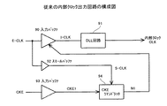
【0006】
図7は、SDRAM等に設けられた従来の内部クロック出力回路の構成図である。外部クロック信号E−CLKは入力バッファ90に入力され、波形整形されてクロック信号I−CLKとなる。クロック信号I−CLKと外部クロック信号E−CLKとの間には、入力バッファ90の遅延時間に相当する位相ずれが生じる。
【0007】
クロック信号I−CLKはDLL回路91に入力される。DLL回路91は、外部クロック信号E−CLKと位相同期した内部クロック信号CLKを、ストローブ信号として図示しないアドレスバッファ等に供給する。また、外部クロック信号E−CLKは、スモールバッファ92にも入力される。スモールバッファ92は、CKEコマンドラッチ回路94のデータ取り込み信号となるクロック信号S−CLKを出力する。
【0008】
一方、クロックイネーブル信号CKEは、外部クロック信号E−CLKを取り込むか否かを制御する信号であり、入力バッファ93に入力されてクロックイネーブル信号CKE1となりCKEコマンドラッチ回路94に出力される。CKEコマンドラッチ回路94は、クロックイネーブル信号CKE1をクロック信号S−CLKの立ち上がりのタイミングで取り込んで、クロック出力制御信号N1を生成し入力バッファ90に出力する。
【0009】
入力バッファ90は、クロック出力制御信号N1がLレベルとなることにより非活性化され、クロック信号I−CLKの出力を停止する。DLL回路91は、入力であるクロック信号I−CLKが停止されると、内部クロック信号CLKの出力を停止する。これにより内部の動作が停止し、SDRAMを低消費電力モードに移行させていた。
【0010】
【発明が解決しようとする課題】
しかしながら、低消費電力モード時に入力バッファ90を非活性化し外部クロック信号E−CLKの取り込みを停止すると、DLL回路91のフィードバック動作が停止してしまう。このように低消費電力モードでDLL回路91を停止させると、通常モードに復帰する時、DLL回路91がアンロック状態からロック状態まで移行するのに長時間を要し、その間はSDRAMの書き込みや読み出し等の動作を行うことができなくなる。
【0011】
また、SDRAMの高速化に伴い、DLL回路91を低消費電力モード時にも継続して動作させ、SDRAM内部の一部の動作を停止するアクティブパワーダウンモードが要求されている。このアクティブパワーダウンモードでは、DLL回路のロック状態が維持され、パワーダウンモードから復帰した時、短時間で通常動作を開始することができる。この場合は、単純に入力バッファ90で外部クロック信号E−CLKの取り込みを停止させるとDLL回路が停止し好ましくない。
【0012】
一方、低消費電力モードに移行させるためのクロックイネーブル信号CKEは、外部クロック信号E−CLKとは非同期に生成されて内部クロック出力回路に入力される。このため、CKEコマンドラッチ回路94で生成されるクロック出力制御信号N1の立ち下がり及び立ち上がりのタイミングは、DLL回路91の出力である内部クロック信号CLKに対して非同期となる。
【0013】
このため、通常モードから低消費電力モードに移行するパワーダウンエントリー時、及び低消費電力モードから通常モードに復帰するパワーダウンイグジット時において、クロックイネーブル信号CKEの入力タイミングによっては、予め設定されているパルス幅より狭いパルス幅の内部クロック信号CLKが出力されてしまう可能性がある。
【0014】
このような予め設定されているパルス幅を確保できない内部クロック信号CLKをSDRAM等に供給すると、所定のパルス幅の内部クロック信号CLKを基準として動作するSDRAM等の誤動作を招き、信頼性の低下につながる。
【0015】
そこで本発明は、低消費電力モードから通常モードに復帰する場合の動作を高速化できる内部クロック出力回路を有する集積回路装置を提供することを目的とする。
【0016】
また本発明は、通常モードから低消費電力モードに移行するパワーダウンエントリー時、及び低消費電力モードから通常モードに復帰するパワーダウンイグジット時において、内部クロック信号のパルス欠けを生じない内部クロック出力回路を有する集積回路装置を提供することを目的とする。
【0017】
【課題を解決するための手段】
上記の目的は、外部クロック信号とクロックイネーブル信号とが供給され、外部クロック信号と所定の位相関係を有する内部クロック信号を内部回路に供給する集積回路装置において、外部クロック信号と位相同期した遅延クロック信号を生成するDLL回路を、低消費電力モードにおいても継続して動作させ、内部回路への遅延クロックの供給を停止する。そして、低消費電力モードから通常モードに復帰する時に、継続して動作しているDLL回路の遅延クロック信号を内部クロック信号として内部回路に供給することにより達成される。
【0018】
本発明によれば、DLL回路は、低消費電力モードにおいても遅延クロック信号を継続して生成している。このため、低消費電力モードから通常モードに復帰する時に、DLL回路はすでにロックオン状態にあり、外部クロック信号に位相同期した内部クロック信号を内部回路に直ちに供給することができ、集積回路装置を書き込みや読み出し等ができる状態に高速に移行させることができる。
【0019】
また、上記の目的は、外部クロック信号とクロックイネーブル信号とが供給され、外部クロック信号と所定の位相関係を有する内部クロック信号を内部回路に供給する集積回路装置において、内部クロック信号を内部回路に供給するか否かを制御するクロック出力制御信号を、遅延クロック信号と所定の位相関係のタイミングで生成し、ゲート回路に出力することにより達成される。
【0020】
本発明によれば、クロック出力制御信号は、遅延クロック信号と所定の位相関係、例えば立ち下がりのタイミングに同期してゲート回路に入力されるので、低消費電力モードに移行する時及び通常モードに復帰する時に、内部クロック信号のパルス欠けを生じることがなく、集積回路装置の誤動作を未然に防止し、信頼性を向上させることができる。
【0021】
【発明の実施の形態】
以下、本発明の実施の形態の例について図面に従って説明する。しかしながら、かかる実施の形態例が本発明の技術的範囲を限定するものではない。
【0022】
図1は、本発明の実施の形態の内部クロック出力回路を有する集積回路装置の使用状態を示す図である。CPU100は、バス104を介してメモリコントローラ101に接続されたメモリ0〜3にアクセスする。メモリコントローラ101は、各メモリ0〜3に外部クロック信号E−CLKを供給すると共に、各メモリ0〜3を低消費電力モードに移行させるためのクロックイネーブル信号CKE0〜3を出力する。メモリ0〜3は、クロックイネーブル信号CKE0〜3がHレベルの時通常モードとなり、クロックイネーブル信号CKE0〜3がLレベルの時低消費電力モードとなる。
【0023】
メモリ0〜3は、例えばSDRAM等の集積回路装置でそれぞれ同様の構成を有する。メモリ0内の内部クロック出力回路102は、外部クロック信号E−CLKを取り込んで、外部クロック信号E−CLKと位相同期した内部クロック信号CLKを生成し、通常モードでは内部クロック信号CLKをアドレスバッファ103に出力する。アドレスバッファ103は、供給された内部クロック信号CLKに同期してアドレスAddを取り込み、アドレス出力Add−outを外部に出力する。
【0024】
一方、クロックイネーブル信号CKE0も内部クロック出力回路102に入力される。内部クロック出力回路102は、クロックイネーブル信号CKE0がLレベルとなると内部クロック信号CLKの出力を停止し、アドレスバッファ102の動作を停止させてメモリ0を低消費電力モードに移行させる。
【0025】
クロックイネーブル信号CKE0がHレベルとなると、内部クロック信号CLKの出力が開始され通常モードとなるが、本実施の形態では、内部クロック出力回路102は、通常モードに復帰する時に、外部クロック信号E−CLKに位相同期した内部クロック信号CLKを直ちに出力することができ、メモリ0の通常モードへの復帰動作を高速化することができる。
【0026】
また、本実施の形態では、内部クロック信号CLKは、低消費電力モードに移行する時及び通常モードに復帰する時に、パルス欠けのないクロック信号を出力するので、アドレスバッファ103等の誤動作を未然に防止し信頼性を向上させることができる。
【0027】
図2は、本発明の実施の形態の内部クロック出力回路102の構成図である。まず、クロックイネーブル信号CKEに応答して、内部クロックCLKの供給を停止するアクティブパワーダウンモードについて説明する。
【0028】
アクティブパワーダウンモードでは、上位のメモリコントローラからアクティブコマンドACが供給されると共にクロックイネーブル信号CKEがLレベルになる。その結果、パワーダウン制御回路18は、クロックイネーブル信号CKEがLレベルになっていても活性化信号PDを活性状態にし、入力バッファ10、14の活性状態を維持する。
【0029】
外部クロック信号E−CLKは入力バッファ10に入力され、波形成形が行われてクロック信号I−CLKとなる。クロック信号I−CLKと外部クロック信号E−CLKとの間には、入力バッファ10の遅延時間に相当する遅れが生じる。
【0030】
クロック信号I−CLKはDLL回路11に入力される。DLL回路11は、外部クロック信号E−CLKと位相同期した遅延クロック信号DLL−CLKを生成する。遅延クロック信号DLL−CLKは、NAND回路12に出力されると共に、CKEコマンドラッチ回路15及びCKEタイミング制御回路16に出力される。
【0031】
一方、クロックイネーブル信号CKEは入力バッファ14に入力され、波形成形が行われてクロックイネーブル信号CKE1となる。クロックイネーブル信号CKE1とクロックイネーブル信号CKEとの間にも、入力バッファ14の遅延時間に相当する遅れが生じる。
【0032】
クロックイネーブル信号CKE1はCKEコマンドラッチ回路15に入力される。CKEコマンドラッチ回路15は、クロックイネーブル信号CKE1を遅延クロック信号DLL−CLKの立ち上がりのタイミングで取り込み、ラッチ信号N1を出力する。
【0033】
ラッチ信号N1はCKEタイミング制御回路16に入力される。CKEタイミング制御回路16は、遅延クロック信号DLL−CLKがHレベルの時のラッチ信号N1をラッチし、遅延クロック信号DLL−CLKがLレベルと時に保持してクロック出力制御信号N2を出力する。クロック出力制御信号N2はNAND回路12に入力される。
【0034】
クロック出力制御信号N2は、NAND回路12により、遅延クロック信号DLL−CLKを内部クロック信号CLKとして出力するか否かを制御する。クロック出力制御信号N2がHレベルの時にNAND回路12を通過した遅延クロック信号DLL−CLKは、インバータ13で反転されて内部クロック信号CLKとなり、前述したSDRAMのアドレスバッファ等に供給される。また、クロック出力制御信号N2がLレベルの時は、遅延クロック信号DLL−CLKはNAND回路12を通過できず、内部クロック信号CLKはSDRAMのアドレスバッファ等に供給されない。
【0035】
このように本実施の形態の内部クロック出力回路102では、アクティブコマンドACが供給されると共にクロックイネーブル信号CKEがLレベルとなるアクティブパワーダウンモードにおいて、DLL回路11は、外部クロック信号E−CLKに位相同期した遅延クロック信号DLL−CLKを継続して生成している。このためアクティブパワーダウンモードから通常モードに復帰する時に、外部クロック信号E−CLKに位相同期した内部クロック信号CLKをアドレスバッファ等に直ちに供給することができ、SDRAMを書き込みや読み出し等のできる状態に高速に移行させることができる。
【0036】
また、クロック出力制御信号N2は、遅延クロック信号DLL−CLKの立ち下がりのタイミングに同期してNAND回路12に入力される。従って、アクティブパワーダウンモードに移行する時及び通常モードに復帰する時に、遅延クロック信号DLL−CLKの次の立上がり時から内部クロック信号CLKが停止又は再開されるので、内部クロック信号CLKのパルス欠けを生じることがなく、SDRAMの誤動作を未然に防止し信頼性を向上させることができる。
【0037】
このようにアクティブパワーダウンモードでは、入力バッファ10、14及びDLL回路11等を動作させ、クロックイネーブル信号CKEに対応して内部クロックCLKの供給を停止する。一方、消費電力を更に低減するためには、入力バッファ10、14及びDLL回路11等の動作を停止させるスタンバイパワーダウンモードが設けられる。
【0038】
スタンバイパワーダウンモードでは、上位のメモリコントローラからのアクティブコマンドACがない状態で、クロックイネーブル信号CKEがLレベルとなる。その結果、パワーダウン制御回路18は活性化信号PDを非活性状態にする。このため入力バッファ10、14は非活性化され、更に、クロック信号I−CLKが供給されないことからDLL回路11の動作も停止する。従って、スタンバイパワーダウンモードでは、アクティブパワーダウンモードより更に消費電力を低減することが可能である。
【0039】
また、スタンバイパワーダウンモードでは、入力バッファ14が非活性状態にあるので、スモールバッファ17によりクロックイネーブル信号CKEのHレベルへの変化が検出される。その結果、パワーダウン制御回路18は、活性化信号PDを活性状態にもどして、入力バッファ10、14を活性化する。そして、DLL回路11の動作再開と共にNAND回路12が開かれ、内部クロック信号CLKが他の入力バッファや内部回路に供給される。
【0040】
図3は、本発明の実施の形態の内部クロック出力回路102に内蔵されるDLL回路11の構成図である。DLL回路11は同じ遅延特性を有する可変遅延回路20、21を備え、可変遅延回路20の遅延量を最適値に設定することにより、外部から供給される外部クロック信号E−CLKの位相に同期した遅延クロック信号DLL−CLKを生成する。
【0041】
外部から供給される外部クロック信号E−CLKは、入力バッファ10を介してクロック信号I−CLKとなりDLL回路11に入力される。クロック信号I−CLKは、可変遅延回路20、21に供給されると共に、位相比較器23にも供給される。
【0042】
可変遅延回路21から出力されたクロック信号B−CLKは、ダミー入力バッファ22を介して、位相比較器23にクロック信号C−CLKとして供給される。位相比較器23は、クロック信号I−CLKとクロック信号C−CLKの位相を比較し、位相比較信号N4を遅延制御回路24に出力する。遅延制御回路24は、可変遅延回路21と可変遅延回路20とにそれぞれ遅延制御信号N5を出力し、クロック信号I−CLKとクロック信号C−CLKの位相が一致するように、可変遅延回路20、21の遅延量を制御する。即ち、その遅延量は、外部クロック信号E−CLKの1周期の時間から入力バッファ10の遅延時間を差し引いた時間である。
【0043】
可変遅延回路20、21は、多数の遅延素子を直列に接続した構造になっており、遅延制御信号N5により信号が通過する遅延素子の数が制御される。可変遅延回路20、21は、遅延制御信号N5により同じ遅延量を与えるように制御されるため、可変遅延回路20に入力されるクロック信号I−CLKは、可変遅延回路20により遅延クロック信号DLL−CLKが外部クロック信号E−CLKの位相と同期する遅延量を与えられてDLL回路11から出力される。従って、DLL回路11は、クロック信号I−CLKが供給されていれば、その位相比較と遅延制御動作を継続する。
【0044】
図4は、本発明の実施の形態の内部クロック出力回路102に内蔵されるCKEタイミング制御回路16の構成図である。図2に示したように、クロックイネーブル信号CKEは、入力バッファ14を介してクロックイネーブル信号CKE1となりCKEコマンドラッチ回路15に入力される。クロックイネーブル信号CKE1は、CKEコマンドラッチ回路15により遅延クロック信号DLL−CLKの立ち上がりエッジで取り込まれ、ラッチ信号N1となって図4に示すスイッチS2に入力される。
【0045】
スイッチS2は、遅延クロック信号DLL−CLKがHレベルの期間オンとなり、ラッチ信号N1をラッチ回路30に出力する。従って、ラッチ回路30は、遅延クロック信号DLL−CLKがLレベルからHレベルに変化した時にラッチ信号N1を受け取り、遅延クロック信号DLL−CLKがHレベルからLレベルに変化した時のラッチ信号N1を保持する。
【0046】
ラッチ回路30の出力信号N3はスイッチS1に入力される。スイッチS1は、遅延クロック信号DLL−CLKをインバータ32で反転した信号で制御され、遅延クロック信号DLL−CLKがLレベルの期間オンとなる。従って、ラッチ回路31は、遅延クロック信号DLL−CLKがHレベルからLレベルに変化した時に信号N3を受け取り、遅延クロック信号DLL−CLKがLレベルからHレベルに変化した時の信号N3を保持する。ラッチ回路31の出力が内部クロック出力制御信号N2となり、図2に示したNAND回路12に出力される。
【0047】
なお図4では、遅延クロック信号DLL−CLKの立ち上がりのタイミングで信号N1を受け取り信号N3を生成しているが、図2に示したCKEコマンドラッチ回路15の遅延時間が大きい場合は、スイッチS2及びラッチ回路30を省略し信号N1を直接スイッチS1に入力してもよい。
【0048】
図5は、本発明の実施の形態の内部クロック出力回路102のタイムチャートである。内部クロック出力回路102の動作を図2及び図4を参照しつつ図5のタイムチャートにより説明する。
【0049】
外部クロック信号E−CLKは、入力バッファ10の遅延時間に相当する遅れを生じてクロック信号I−CLKとなる。一方、クロックイネーブル信号CKEは外部クロック信号E−CLKとは非同期で入力され、入力バッファ14の遅延時間に相当する遅れを生じてクロックイネーブル信号CKE1となる。なお、クロックイネーブル信号CKEがHレベルの期間が通常モードであり、クロックイネーブル信号CKEがLレベルの期間が低消費電力モードである。
【0050】
クロック信号I−CLKはDLL回路11に入力され、外部クロック信号E−CLKに位相同期した遅延クロック信号DLL−CLKとなる。また、クロックイネーブル信号CKE1はCKEコマンドラッチ回路15に入力され、遅延クロック信号DLL−CLKの立ち上がりのタイミングで取り込まれてラッチ信号N1となる。
【0051】
ラッチ信号N1は、CKEタイミング制御回路16のスイッチS2(図4参照)に入力される。スイッチS2は遅延クロック信号DLL−CLKがHレベルの期間オンとなるので、ラッチ回路30は遅延クロック信号DLL−CLKがHレベルからLレベルに変化する時の信号N1をラッチする。ラッチ回路30の出力が信号N3である。
【0052】
信号N3はスイッチS1に入力される。スイッチS1は遅延クロック信号DLL−CLKがLレベルの期間オンとなるので、ラッチ回路31は遅延クロック信号DLL−CLKがLレベルからHレベルに変化する時の信号N3をラッチする。ラッチ回路31の出力がクロック出力制御信号N2である。このクロック出力制御信号N2がLレベルとなると、NAND回路12により内部クロック信号CLKの出力が停止される。
【0053】
このように本実施の形態の内部クロック出力回路102は、低消費電力モードにおいても外部クロック信号E−CLKに位相同期した遅延クロック信号DLL−CLKが生成されている。このため低消費電力モードから通常モードに復帰する時に、外部クロック信号E−CLKに位相同期した内部クロック信号CLKを直ちに出力することができる。従って、通常モードに復帰する時のSDRAMの書き込みや読み出し等の動作を高速化することができる。
【0054】
また、クロック出力制御信号N2は、遅延クロック信号DLL−CLKの立ち下がりのタイミングに同期して出力されるため、低消費電力モードに移行する時及び通常モードに復帰する時に、内部クロック信号CLKのパルス欠けを生じない。このため、内部クロック信号CLKが供給されるアドレスバッファ等の誤動作を未然に防止し、SDRAMの信頼性を向上させることができる。
【0055】
図6は、本発明の実施の形態のCKEコマンドラッチ回路15とCKEタイミング制御回路16の回路例を示す。CKEコマンドラッチ回路15は、P型トランジスタ40、41、45、46、51、N型トランジスタ42、43、47、48、49、52、インバータ44、50、53、54を有し、遅延クロック信号DLL−CLKの立ち上がりタイミングのクロックイネーブル信号CKE1をラッチし、ラッチ信号N1を出力する。
【0056】
遅延クロック信号DLL−CLKがLレベルの時は、N型トランジスタ49はオフし、P型トランジスタ40、46はオンとなるため、ノードN10、N11は共にHレベルである。このためP型トランジスタ51とN型トランジスタ52は共にオフとなり、ノードN1はハイインピーダンス状態となる。なお、ノードN10、N11は共にHレベルであるため、N型トランジスタ42、47は共にオンとなっている。
【0057】
遅延クロック信号DLL−CLKがHレベルになるとN型トランジスタ49はオンとなる。この時クロックイネーブル信号CKE1がLレベルの場合は、インバータ44によりN型トランジスタ48のゲートがHレベルとなるため、N型トランジスタ48がオンしノード11をLレベルとする。一方、クロックイネーブル信号CKE1がHレベルの場合は、N型トランジスタ43がオンしノード10をLレベルとする。ノードN10又はN11がLレベルとなると、P型トランジスタ45又は41がオンし、反対側のノードN11又はN10をHレベルに確定する。
【0058】
ノードN10がLレベルでノードN11がHレベルの場合は、P型トランジスタ51はオン、N型トランジスタ52はオフとなり、ノードN1はHレベルとなってインバータ53、54によりラッチされる。一方、ノードN10がHレベルでノードN11がLレベルの場合は、P型トランジスタ51はオフ、N型トランジスタ52はオンとなり、ノードN1はLレベルとなってインバータ53、54によりラッチされる。
【0059】
CKEタイミング制御回路16は、P型トランジスタ55とN型トランジスタ56によるトランスファーゲート65、インバータ32等を有する。なお、トランスファーゲート65とインバータ57とが図4に示したスイッチS2に相当し、トランスファーゲート66とインバータ62とがスイッチS1に相当する。また、インバータ58と59とが図4に示したラッチ回路30に相当し、インバータ63と64とがラッチ回路31に相当する。
【0060】
CKEコマンドラッチ回路15から出力されたラッチ信号N1はトランスファーゲート65に入力され、遅延クロック信号DLL−CLKのHレベルの期間にトランスファーゲート65を通過し、ラッチ回路30でラッチされて信号N3となる。
【0061】
信号N3はトランスファーゲート66に入力され、遅延クロック信号DLL−CLKのLレベルの期間にトランスファーゲート66を通過し、ラッチ回路31でラッチされてクロック出力制御信号N2となる。このクロック出力制御信号N2が、図2に示したNAND回路12により内部クロック信号CLKを出力するか否かを制御する。
【0062】
このように本発明の実施の形態では、低消費電力モードに移行する時、入力バッファ10を非活性化して外部クロック信号E−CLKの取り込みを停止させるのではなく、NAND回路12で内部クロック信号CLKの出力を停止させている。
【0063】
従って、入力バッファ10及びDLL回路11は、外部クロック信号E−CLKが入力される限り活性状態であり、NAND回路12に遅延クロック信号DLL−CLKを供給し続ける。このため、低消費電力モードから通常モードに復帰した際の内部クロック信号CLKの位相ズレを防止でき、SDRAM等を通常動作に高速に復帰させることができる。
【0064】
【発明の効果】
以上説明した通り、本発明によれば、低消費電力モードにおいても外部クロック信号に位相同期した内部クロック信号を継続して生成しているため、低消費電力モードから通常モードに復帰する場合に、外部クロック信号に位相同期した内部クロック信号を直ちに供給することができ、SDRAM等の動作を高速化することができる。
【0065】
また本発明によれば、通常モードから低消費電力モードに移行するパワーダウンエントリー時、及び低消費電力モードから通常モードに復帰するパワーダウンイグジット時において、内部クロック信号のパルス欠けによるSDRAM等の誤動作を未然に防止し、信頼性を向上させることができる。
【図面の簡単な説明】
【図1】本発明の実施の形態の内部クロック出力回路を有する集積回路装置の説明図である。
【図2】本発明の実施の形態の内部クロック出力回路の構成図である。
【図3】本発明の実施の形態のDLL回路の構成図である。
【図4】本発明の実施の形態のCKEタイミング制御回路の構成図である。
【図5】本発明の実施の形態の内部クロック出力回路のタイムチャートである。
【図6】本発明の実施の形態のCKEコマンドラッチ回路とCKEタイミング制御回路の回路図である。
【図7】従来の内部クロック出力回路の構成図である。
【符号の説明】
10、14 入力バッファ
11 DLL回路
12 NAND回路
13 インバータ
15 CKEコマンドラッチ回路
16 CKEタイミング制御回路
30、31 ラッチ回路
102 内部クロック出力回路
103 アドレスバッファ[0001]
BACKGROUND OF THE INVENTION
The present invention relates to an integrated circuit device having a circuit that outputs an internal clock signal having a predetermined phase relationship with a supplied clock signal, and an internal clock capable of speeding up the return operation from the low power consumption mode to the normal mode. The present invention relates to an integrated circuit device having an output circuit.
[0002]
[Prior art]
As a clock synchronous dynamic random access memory (DRAM), a synchronous DRAM (SDRAM) has attracted attention. The SDRAM is supplied with signals such as address, data, command and the like in synchronization with an external clock signal given from the system side, and outputs a read data signal in synchronization with the external clock signal, and can operate at high speed. .
[0003]
As the speed of the SDRAM increases, the internal clock signal, which is generated by taking in the external clock signal internally, deviates from the phase of the external clock signal, so that signals such as input address, data, command, and output data signal The strobe signal may not be used.
[0004]
In order to compensate for this phase shift, an internal clock signal that is phase-synchronized with the external clock signal or has a predetermined phase difference from the phase of the external clock signal by a delay locked loop (hereinafter simply referred to as DLL) circuit or the like. The input address signal or the like is taken in at the timing of the internal clock signal, and the output data signal is output.
[0005]
On the other hand, speeding up of the clock signal increases the frequency of writing and reading of the SDRAM, and increases the power consumption of the SDRAM. Therefore, a low power consumption mode is provided to stop the internal operation of the SDRAM when access is not performed. In the low power consumption mode, the clock enable signal is set to an inactive level (L level) so that the input buffer is externally connected. The capturing of the clock signal is stopped, and unnecessary internal operations are stopped.
[0006]
FIG. 7 is a configuration diagram of a conventional internal clock output circuit provided in an SDRAM or the like. The external clock signal E-CLK is input to the input buffer 90, and the waveform is shaped to become the clock signal I-CLK. A phase shift corresponding to the delay time of the input buffer 90 occurs between the clock signal I-CLK and the external clock signal E-CLK.
[0007]
The clock signal I-CLK is input to the
[0008]
On the other hand, the clock enable signal CKE is a signal for controlling whether or not the external clock signal E-CLK is taken in. The clock enable signal CKE is input to the input buffer 93 to become the clock enable signal CKE1 and is output to the CKE
[0009]
The input buffer 90 is deactivated when the clock output control signal N1 becomes L level, and stops outputting the clock signal I-CLK. The
[0010]
[Problems to be solved by the invention]
However, if the input buffer 90 is deactivated in the low power consumption mode to stop taking in the external clock signal E-CLK, the feedback operation of the
[0011]
As the speed of the SDRAM increases, an active power down mode is required in which the
[0012]
On the other hand, the clock enable signal CKE for shifting to the low power consumption mode is generated asynchronously with the external clock signal E-CLK and input to the internal clock output circuit. Therefore, the falling and rising timings of the clock output control signal N1 generated by the CKE
[0013]
For this reason, it is set in advance depending on the input timing of the clock enable signal CKE at the time of power down entry for shifting from the normal mode to the low power consumption mode and at the time of power down exit for returning from the low power consumption mode to the normal mode. There is a possibility that the internal clock signal CLK having a pulse width narrower than the pulse width is output.
[0014]
If such an internal clock signal CLK that cannot secure a preset pulse width is supplied to the SDRAM or the like, the SDRAM or the like that operates based on the internal clock signal CLK having a predetermined pulse width may malfunction, resulting in a decrease in reliability. Connected.
[0015]
Therefore, an object of the present invention is to provide an integrated circuit device having an internal clock output circuit capable of speeding up the operation when returning from the low power consumption mode to the normal mode.
[0016]
The present invention also provides an internal clock output circuit that does not cause a missing pulse of the internal clock signal at the time of power-down entry for shifting from the normal mode to the low power consumption mode and at the time of power down exit for returning from the low power consumption mode to the normal mode. It is an object of the present invention to provide an integrated circuit device having the following.
[0017]
[Means for Solving the Problems]
The above object is to provide a delay clock that is phase-synchronized with an external clock signal in an integrated circuit device that is supplied with an external clock signal and a clock enable signal and supplies the internal clock signal having a predetermined phase relationship with the external clock signal to the internal circuit. The DLL circuit that generates the signal is continuously operated even in the low power consumption mode, and the supply of the delay clock to the internal circuit is stopped. Then, when returning from the low power consumption mode to the normal mode, the delay clock signal of the continuously operating DLL circuit is supplied to the internal circuit as an internal clock signal.
[0018]
According to the present invention, the DLL circuit continuously generates the delayed clock signal even in the low power consumption mode. Therefore, when returning from the low power consumption mode to the normal mode, the DLL circuit is already in a lock-on state, and an internal clock signal phase-synchronized with the external clock signal can be immediately supplied to the internal circuit. It is possible to shift to a state where writing and reading can be performed at high speed.
[0019]
Another object of the present invention is to provide an integrated circuit device that is supplied with an external clock signal and a clock enable signal and supplies the internal clock signal having a predetermined phase relationship with the external clock signal to the internal circuit. This is achieved by generating a clock output control signal for controlling whether or not to supply the signal at a timing having a predetermined phase relationship with the delayed clock signal and outputting it to the gate circuit.
[0020]
According to the present invention, the clock output control signal is input to the gate circuit in synchronism with the delay clock signal and a predetermined phase relationship, for example, the falling timing, so that the low power consumption mode is entered and the normal mode is entered. When returning, the internal clock signal is not missing a pulse, so that the malfunction of the integrated circuit device can be prevented and the reliability can be improved.
[0021]
DETAILED DESCRIPTION OF THE INVENTION
Hereinafter, an example of an embodiment of the present invention will be described with reference to the drawings. However, such an embodiment does not limit the technical scope of the present invention.
[0022]
FIG. 1 is a diagram showing a use state of an integrated circuit device having an internal clock output circuit according to an embodiment of the present invention. The
[0023]
The memories 0 to 3, for example, are integrated circuit devices such as SDRAM and have the same configuration. The internal
[0024]
On the other hand, the clock enable signal CKE 0 is also input to the internal
[0025]
When the clock enable signal CKE0 becomes H level, the output of the internal clock signal CLK is started and the normal mode is entered. In the present embodiment, the internal
[0026]
In the present embodiment, the internal clock signal CLK outputs a clock signal with no missing pulses when shifting to the low power consumption mode and when returning to the normal mode. It can prevent and improve the reliability.
[0027]
FIG. 2 is a configuration diagram of the internal
[0028]
In the active power down mode, the active command AC is supplied from the upper memory controller, and the clock enable signal CKE becomes L level. As a result, the power-
[0029]
The external clock signal E-CLK is input to the
[0030]
The clock signal I-CLK is input to the DLL circuit 11. The DLL circuit 11 generates a delayed clock signal DLL-CLK that is phase-synchronized with the external clock signal E-CLK. The delayed clock signal DLL-CLK is output to the
[0031]
On the other hand, the clock enable signal CKE is input to the
[0032]
The clock enable signal CKE1 is input to the CKE
[0033]
The latch signal N1 is input to the CKE
[0034]
The clock output control signal N2 controls whether or not the delayed clock signal DLL-CLK is output as the internal clock signal CLK by the
[0035]
As described above, in the internal
[0036]
The clock output control signal N2 is input to the
[0037]
As described above, in the active power down mode, the input buffers 10 and 14 and the DLL circuit 11 are operated, and the supply of the internal clock CLK is stopped in response to the clock enable signal CKE. On the other hand, in order to further reduce power consumption, a standby power down mode is provided in which the operations of the input buffers 10 and 14 and the DLL circuit 11 are stopped.
[0038]
In the standby power down mode, the clock enable signal CKE goes to L level in the state where there is no active command AC from the upper memory controller. As a result, the power down
[0039]
In the standby power down mode, since the
[0040]
FIG. 3 is a configuration diagram of the DLL circuit 11 built in the internal
[0041]
The external clock signal E-CLK supplied from the outside becomes the clock signal I-CLK via the
[0042]
The clock signal B-CLK output from the
[0043]
The
[0044]
FIG. 4 is a configuration diagram of the CKE
[0045]
The switch S2 is turned on while the delayed clock signal DLL-CLK is at the H level, and outputs the latch signal N1 to the
[0046]
The output signal N3 of the
[0047]
In FIG. 4, the signal N1 is received and the signal N3 is generated at the rising timing of the delay clock signal DLL-CLK. However, when the delay time of the CKE
[0048]
FIG. 5 is a time chart of the internal
[0049]
The external clock signal E-CLK generates a delay corresponding to the delay time of the
[0050]
The clock signal I-CLK is input to the DLL circuit 11 and becomes a delayed clock signal DLL-CLK that is phase-synchronized with the external clock signal E-CLK. The clock enable signal CKE1 is input to the CKE
[0051]
The latch signal N1 is input to the switch S2 (see FIG. 4) of the CKE
[0052]
The signal N3 is input to the switch S1. Since the switch S1 is turned on while the delayed clock signal DLL-CLK is at the L level, the
[0053]
As described above, the internal
[0054]
Further, since the clock output control signal N2 is output in synchronization with the falling timing of the delayed clock signal DLL-CLK, when the shift to the low power consumption mode and the return to the normal mode, the internal clock signal CLK Does not cause missing pulses. For this reason, it is possible to prevent malfunction of the address buffer or the like to which the internal clock signal CLK is supplied, and to improve the reliability of the SDRAM.
[0055]
FIG. 6 shows a circuit example of the CKE
[0056]
When the delayed clock signal DLL-CLK is at the L level, the N-
[0057]
When the delayed clock signal DLL-CLK becomes H level, the N-
[0058]
When node N10 is at L level and node N11 is at H level, P-type transistor 51 is on, N-
[0059]
The CKE
[0060]
The latch signal N1 output from the CKE
[0061]
The signal N3 is input to the
[0062]
As described above, in the embodiment of the present invention, when shifting to the low power consumption mode, the
[0063]
Accordingly, the
[0064]
【The invention's effect】
As described above, according to the present invention, since the internal clock signal that is phase-synchronized with the external clock signal is continuously generated even in the low power consumption mode, when returning from the low power consumption mode to the normal mode, The internal clock signal that is phase-synchronized with the external clock signal can be supplied immediately, and the operation of the SDRAM or the like can be speeded up.
[0065]
Further, according to the present invention, the malfunction of the SDRAM or the like due to the lack of a pulse of the internal clock signal at the time of power down entry for shifting from the normal mode to the low power consumption mode and at the power down exit for returning from the low power consumption mode to the normal mode Can be prevented and reliability can be improved.
[Brief description of the drawings]
FIG. 1 is an explanatory diagram of an integrated circuit device having an internal clock output circuit according to an embodiment of the present invention.
FIG. 2 is a configuration diagram of an internal clock output circuit according to the embodiment of the present invention.
FIG. 3 is a configuration diagram of a DLL circuit according to the embodiment of the present invention.
FIG. 4 is a configuration diagram of a CKE timing control circuit according to the embodiment of the present invention.
FIG. 5 is a time chart of the internal clock output circuit according to the embodiment of the present invention.
FIG. 6 is a circuit diagram of a CKE command latch circuit and a CKE timing control circuit according to the embodiment of the present invention.
FIG. 7 is a configuration diagram of a conventional internal clock output circuit.
[Explanation of symbols]
10, 14 Input buffer
11 DLL circuit
12 NAND circuit
13 Inverter
15 CKE command latch circuit
16 CKE timing control circuit
30, 31 latch circuit
102 Internal clock output circuit
103 Address buffer
Claims (6)
前記外部クロックを入力して入力クロック信号を出力する入力バッファと、
前記入力クロック信号と所定の位相関係を有する遅延クロック信号を生成するDLL回路と、
前記遅延クロック信号に応答して前記クロックイネーブル信号を取り込んで、クロック出力制御信号を生成するクロックイネーブルタイミング制御回路と、
前記クロック出力制御信号に応答して、前記遅延クロック信号を前記内部クロック信号として前記内部回路に供給又は停止するゲート回路と、
前記クロックイネーブル信号とアクティブコマンドとに基づいて活性化信号を生成するパワーダウン制御回路とを有し、
前記アクティブコマンドが供給され且つ前記クロックイネーブル信号が非活性状態になる第1の低消費電力モード時には、前記活性化信号に基づいて前記入力バッファの活性化状態を維持して前記DLL回路の活性化状態を維持し、前記アクティブコマンドが供給されず且つ前記クロックイネーブル信号が非活性状態になる第2の低消費電力モード時には、前記活性化信号に基づいて前記入力バッファを非活性状態にし、
前記第1の低消費電力モードから通常モードに移行する時には前記ゲート回路は前記クロック出力制御信号に応答して前記内部回路への前記遅延クロック信号の供給を開始し、通常モードから前記第1の低消費電力モードに移行する時には、前記ゲート回路は前記クロック出力制御信号に応答して前記内部回路への前記遅延クロック信号の供給を停止することを特徴とする集積回路装置。In an integrated circuit device for supplying an external clock signal and a clock enable signal and supplying an internal clock signal having a predetermined phase relationship with the external clock signal to an internal circuit,
An input buffer for inputting the external clock and outputting an input clock signal;
A DLL circuit for generating a delayed clock signal having a predetermined phase relationship with the input clock signal;
A clock enable timing control circuit that takes in the clock enable signal in response to the delayed clock signal and generates a clock output control signal;
A gate circuit for supplying or stopping the delayed clock signal as the internal clock signal to the internal circuit in response to the clock output control signal;
A power-down control circuit that generates an activation signal based on the clock enable signal and an active command;
In the first low power consumption mode in which the active command is supplied and the clock enable signal is inactivated, the activation of the DLL circuit is maintained by maintaining the activated state of the input buffer based on the activation signal. In the second low power consumption mode in which the active command is not supplied and the clock enable signal is inactive, the input buffer is inactivated based on the activation signal.
The gate circuit starts supplying the delayed clock signal to the internal circuit in response to the clock output control signal when shifting from the first low power consumption mode to the normal mode . when shifting to a low power consumption mode, the gate circuit is an integrated circuit apparatus characterized by stopping the supply of said delayed clock signal to the internal circuit in response to said clock output control signal.
前記外部クロックを入力して入力クロック信号を出力する入力バッファと、
前記外部クロック信号と所定の位相関係を有する遅延クロック信号を生成するDLL回路と、
前記クロックイネーブル信号を、前記遅延クロック信号に応答して取り込んで、クロック出力制御信号を生成する第1の制御回路と、
前記クロックイネーブル信号とアクティブコマンドとに基づいて前記入力バッファの活性化信号を生成する第2の制御回路と、
前記クロック出力制御信号に応答して、前記遅延クロック信号を前記内部クロック信号として前記内部回路に供給開始又は供給停止するゲート回路とを有し、
通常モード時には前記ゲート回路は前記内部回路へ前記遅延クロック信号を供給し、アクティブパワーダウンモード時には前記活性化信号に基づいて前記入力バッファの活性化状態を保つことで前記DLL回路を活性状態に保つと共に、前記ゲート回路が前記クロック出力制御信号に基づいて前記内部回路への前記遅延クロック信号の供給を停止することを特徴とする集積回路装置。In an integrated circuit device for supplying an external clock signal and a clock enable signal and supplying an internal clock signal having a predetermined phase relationship with the external clock signal to an internal circuit,
An input buffer for inputting the external clock and outputting an input clock signal;
A DLL circuit for generating a delayed clock signal having a predetermined phase relationship with the external clock signal;
A first control circuit that captures the clock enable signal in response to the delayed clock signal and generates a clock output control signal;
A second control circuit for generating an activation signal for the input buffer based on the clock enable signal and an active command ;
In response to the clock output control signal, the delay clock signal as the internal clock signal to start or stop supplying to the internal circuit, and
In the normal mode, the gate circuit supplies the delayed clock signal to the internal circuit, and in the active power down mode, the active state of the input buffer is maintained based on the activation signal to keep the DLL circuit active. An integrated circuit device wherein the gate circuit stops the supply of the delayed clock signal to the internal circuit based on the clock output control signal.
前記外部クロック信号を入力するクロック用入力バッファと、
前記クロック用入力バッファからのクロック信号を供給され、前記外部クロック信号と所定の位相関係を有する遅延クロック信号を生成するDLL回路と、
前記遅延クロック信号に応答して前記クロックイネーブル信号を取り込んで、クロック出力制御信号を生成するクロックイネーブルタイミング制御回路と、
前記クロックイネーブル信号とアクティブコマンドとに基づいて活性化信号を生成するパワーダウン制御回路と、
前記アクティブコマンドが供給され且つ前記クロックイネーブル信号が非活性状態になる第1のパワーダウンモードに移行する時に、前記クロック出力制御信号に応答して、前記遅延クロック信号を前記内部クロック信号として前記内部回路に供給することを停止し、前記第1のパワーダウンモードから復帰する時に前記クロック出力制御信号に応答して前記供給することを開始するゲート回路とを有し、
前記第1のパワーダウンモード時に、前記クロック入力バッファを活性状態にして前記DLL回路を活性状態に維持し、
前記アクティブコマンドが供給されず且つ前記クロックイネーブル信号が非活性状態になる第2のパワーダウンモード時に、前記活性化信号に応答して、前記クロック用入力バッファを非活性状態にして前記DLL回路を停止することを特徴とする集積回路装置。In an integrated circuit device for supplying an external clock signal and a clock enable signal and supplying an internal clock signal having a predetermined phase relationship with the external clock signal to an internal circuit,
A clock input buffer for inputting the external clock signal;
A DLL circuit which is supplied with a clock signal from the clock input buffer and generates a delayed clock signal having a predetermined phase relationship with the external clock signal;
A clock enable timing control circuit that takes in the clock enable signal in response to the delayed clock signal and generates a clock output control signal;
A power-down control circuit that generates an activation signal based on the clock enable signal and an active command;
In response to the clock output control signal, when the active command is supplied and the clock enable signal is inactivated, the internal clock signal is used as the delayed clock signal as the internal clock signal. A gate circuit that stops supplying to the circuit and starts supplying in response to the clock output control signal when returning from the first power-down mode;
In the first power-down mode, the clock input buffer is activated to maintain the DLL circuit in an activated state;
In response to the activation signal, the clock input buffer is deactivated in response to the activation signal in the second power down mode in which the active command is not supplied and the clock enable signal is deactivated. An integrated circuit device, wherein the integrated circuit device is stopped.
前記外部クロック信号を入力するクロック用入力バッファと、
前記クロック用入力バッファからのクロック信号を供給され、前記外部クロック信号と所定の位相関係を有する遅延クロック信号を生成するDLL回路と、
前記アクティブコマンドが供給され且つ前記クロックイネーブル信号が非活性状態になる第1のパワーダウンモードに移行する時に、前記クロックイネーブル信号の前記非活性状態に従い且つ前記遅延クロック信号に応答して、前記遅延クロック信号を前記内部クロック信号として前記内部回路に供給することを停止し、前記第1のパワーダウンモードから復帰する時に前記クロックイネーブル信号の前記活性化状態に従い且つ前記遅延クロック信号に応答して前記供給することを開始するゲート回路と、
前記アクティブコマンドが供給されず且つ前記クロックイネーブル信号が非活性状態になる第2のパワーダウンモード時に、前記クロックイネーブル信号の前記非活性状態に応答して、前記クロック用入力バッファを非活性状態にするパワーダウン制御回路とを有することを特徴とする集積回路装置。In an integrated circuit device for supplying an external clock signal and a clock enable signal and supplying an internal clock signal having a predetermined phase relationship with the external clock signal to an internal circuit,
A clock input buffer for inputting the external clock signal;
A DLL circuit which is supplied with a clock signal from the clock input buffer and generates a delayed clock signal having a predetermined phase relationship with the external clock signal;
The delay according to the inactive state of the clock enable signal and in response to the delayed clock signal when transitioning to a first power down mode in which the active command is supplied and the clock enable signal is in an inactive state Stop supplying a clock signal to the internal circuit as the internal clock signal, and follow the activation state of the clock enable signal and in response to the delayed clock signal when returning from the first power-down mode A gate circuit that starts to supply, and
In response to the inactive state of the clock enable signal, the clock input buffer is inactivated in the second power down mode in which the active command is not supplied and the clock enable signal is inactivated. An integrated circuit device comprising: a power-down control circuit configured to
Priority Applications (3)
| Application Number | Priority Date | Filing Date | Title |
|---|---|---|---|
| JP18448398A JP4178225B2 (en) | 1998-06-30 | 1998-06-30 | Integrated circuit device |
| US09/304,516 US6266294B1 (en) | 1998-06-30 | 1999-05-04 | Integrated circuit device |
| KR1019990017075A KR100329243B1 (en) | 1998-06-30 | 1999-05-13 | Integrated circuit device |
Applications Claiming Priority (1)
| Application Number | Priority Date | Filing Date | Title |
|---|---|---|---|
| JP18448398A JP4178225B2 (en) | 1998-06-30 | 1998-06-30 | Integrated circuit device |
Publications (3)
| Publication Number | Publication Date |
|---|---|
| JP2000021165A JP2000021165A (en) | 2000-01-21 |
| JP2000021165A5 JP2000021165A5 (en) | 2004-12-16 |
| JP4178225B2 true JP4178225B2 (en) | 2008-11-12 |
Family
ID=16153974
Family Applications (1)
| Application Number | Title | Priority Date | Filing Date |
|---|---|---|---|
| JP18448398A Expired - Lifetime JP4178225B2 (en) | 1998-06-30 | 1998-06-30 | Integrated circuit device |
Country Status (3)
| Country | Link |
|---|---|
| US (1) | US6266294B1 (en) |
| JP (1) | JP4178225B2 (en) |
| KR (1) | KR100329243B1 (en) |
Families Citing this family (33)
| Publication number | Priority date | Publication date | Assignee | Title |
|---|---|---|---|---|
| JP4489231B2 (en) * | 2000-02-23 | 2010-06-23 | 富士通マイクロエレクトロニクス株式会社 | Delay time adjustment method and delay time adjustment circuit |
| JP4649081B2 (en) * | 2000-10-02 | 2011-03-09 | キヤノン株式会社 | PERIPHERAL DEVICE, ITS CONTROL METHOD, PROGRAM, AND STORAGE MEDIUM |
| US6480439B2 (en) * | 2000-10-03 | 2002-11-12 | Mitsubishi Denki Kabushiki Kaisha | Semiconductor device |
| US6898683B2 (en) * | 2000-12-19 | 2005-05-24 | Fujitsu Limited | Clock synchronized dynamic memory and clock synchronized integrated circuit |
| KR100413758B1 (en) * | 2001-03-26 | 2003-12-31 | 삼성전자주식회사 | Semiconductor memory device including delay locked loop |
| KR100422572B1 (en) * | 2001-06-30 | 2004-03-12 | 주식회사 하이닉스반도체 | Register controlled delay locked loop and semiconductor device having the same |
| US6832327B1 (en) * | 2001-10-02 | 2004-12-14 | Advanced Micro Devices, Inc. | Apparatus and method for providing an external clock from a circuit in sleep mode in a processor-based system |
| US6678205B2 (en) * | 2001-12-26 | 2004-01-13 | Micron Technology, Inc. | Multi-mode synchronous memory device and method of operating and testing same |
| JP2003228982A (en) | 2002-01-29 | 2003-08-15 | Hitachi Ltd | Semiconductor integrated circuit device |
| KR100470995B1 (en) * | 2002-04-23 | 2005-03-08 | 삼성전자주식회사 | multi clock domain data input processing device having clock receiving locked loop and method for providing clock signals therefore |
| US6765433B1 (en) * | 2003-03-20 | 2004-07-20 | Atmel Corporation | Low power implementation for input signals of integrated circuits |
| KR100560297B1 (en) * | 2003-10-29 | 2006-03-10 | 주식회사 하이닉스반도체 | Semiconductor device having power supply circuit for delay locked loop |
| KR100540487B1 (en) * | 2003-10-31 | 2006-01-10 | 주식회사 하이닉스반도체 | Data output control circuit |
| KR100571651B1 (en) * | 2003-12-29 | 2006-04-17 | 주식회사 하이닉스반도체 | Control circuit for escaping power-down mode confidentially |
| KR100808052B1 (en) * | 2005-09-28 | 2008-03-07 | 주식회사 하이닉스반도체 | Semicoductor memory device |
| JP4930875B2 (en) * | 2005-09-29 | 2012-05-16 | 株式会社ハイニックスセミコンダクター | On-die termination control device |
| JP4524662B2 (en) * | 2005-10-21 | 2010-08-18 | エルピーダメモリ株式会社 | Semiconductor memory chip |
| KR100702766B1 (en) * | 2005-12-07 | 2007-04-03 | 주식회사 하이닉스반도체 | Internal voltage generator for generating stable internal voltage for delay locked loop, internal clock generator with the same, and method for generating the stable internal voltage for delay locked loop |
| KR100680975B1 (en) * | 2006-01-13 | 2007-02-09 | 주식회사 하이닉스반도체 | Power down mode control circuit |
| KR100776906B1 (en) * | 2006-02-16 | 2007-11-19 | 주식회사 하이닉스반도체 | Delay locked loop with a function for implementing locking operation periodically during power down mode and locking operation method of the same |
| US7613064B1 (en) * | 2006-12-19 | 2009-11-03 | Nvidia Corporation | Power management modes for memory devices |
| KR100896182B1 (en) * | 2007-02-22 | 2009-05-12 | 삼성전자주식회사 | Method and apparatus to control DLL power down |
| US20080228950A1 (en) * | 2007-03-14 | 2008-09-18 | Qimonda North America Corp. | Memory power down mode exit method and system |
| JP2009140322A (en) * | 2007-12-07 | 2009-06-25 | Elpida Memory Inc | Timing control circuit and semiconductor memory device |
| KR100902058B1 (en) * | 2008-01-07 | 2009-06-09 | 주식회사 하이닉스반도체 | Semiconductor integrated circuit and method of controlling the same |
| US7728638B2 (en) * | 2008-04-25 | 2010-06-01 | Qimonda North America Corp. | Electronic system that adjusts DLL lock state acquisition time |
| JP5654196B2 (en) * | 2008-05-22 | 2015-01-14 | ピーエスフォー ルクスコ エスエイアールエルPS4 Luxco S.a.r.l. | DLL circuit unit and semiconductor memory |
| KR100996176B1 (en) | 2008-12-09 | 2010-11-24 | 주식회사 하이닉스반도체 | Semiconductor memory device and control method of delay locked loop including the same |
| US8824235B2 (en) | 2009-12-30 | 2014-09-02 | Micron Technology, Inc. | Controlling clock input buffers |
| KR101175244B1 (en) | 2010-04-29 | 2012-08-22 | 에스케이하이닉스 주식회사 | Semiconductor device and opeating method of the same, memory system |
| KR101136985B1 (en) | 2010-08-18 | 2012-04-19 | 에스케이하이닉스 주식회사 | Data Outputting Circuit of a Semiconductor Memory Apparatus |
| WO2012164342A1 (en) * | 2011-05-27 | 2012-12-06 | Freescale Semiconductor, Inc. | Integrated circuit device and method for controlling an operating mode of an on-die memory |
| JP2015035241A (en) * | 2013-08-09 | 2015-02-19 | マイクロン テクノロジー, インク. | Semiconductor device |
Family Cites Families (3)
| Publication number | Priority date | Publication date | Assignee | Title |
|---|---|---|---|---|
| JP3429977B2 (en) * | 1997-05-16 | 2003-07-28 | 富士通株式会社 | Skew reduction circuit and semiconductor device |
| JP3832932B2 (en) * | 1997-07-11 | 2006-10-11 | 富士通株式会社 | Semiconductor integrated circuit and semiconductor integrated circuit system |
| JP4031859B2 (en) * | 1998-02-03 | 2008-01-09 | 富士通株式会社 | Semiconductor device |
-
1998
- 1998-06-30 JP JP18448398A patent/JP4178225B2/en not_active Expired - Lifetime
-
1999
- 1999-05-04 US US09/304,516 patent/US6266294B1/en not_active Expired - Lifetime
- 1999-05-13 KR KR1019990017075A patent/KR100329243B1/en not_active IP Right Cessation
Also Published As
| Publication number | Publication date |
|---|---|
| US6266294B1 (en) | 2001-07-24 |
| KR100329243B1 (en) | 2002-03-18 |
| KR20000005652A (en) | 2000-01-25 |
| JP2000021165A (en) | 2000-01-21 |
Similar Documents
| Publication | Publication Date | Title |
|---|---|---|
| JP4178225B2 (en) | Integrated circuit device | |
| KR100808052B1 (en) | Semicoductor memory device | |
| US7489172B2 (en) | DLL driver control circuit | |
| JP3549751B2 (en) | Semiconductor integrated circuit device | |
| US7340632B2 (en) | Domain crossing device | |
| US7489170B2 (en) | Delay locked loop in synchronous semiconductor memory device and driving method thereof | |
| JP4104886B2 (en) | Semiconductor device | |
| TWI395220B (en) | Semiconductor memory device and method of operating the same | |
| KR100573831B1 (en) | Semiconductor memory device having safely entery and exit for self-refresh mode | |
| US6954094B2 (en) | Semiconductor memory device having partially controlled delay locked loop | |
| JP2001189079A (en) | Delay fixing loop circuit for compensating skewness in sdram | |
| US6519188B2 (en) | Circuit and method for controlling buffers in semiconductor memory device | |
| KR100486922B1 (en) | Semiconductor storage unit | |
| JP3725715B2 (en) | Clock synchronization system | |
| JP3880206B2 (en) | Integrated circuit device | |
| USRE46141E1 (en) | Semiconductor device and timing control method for the same | |
| KR100550633B1 (en) | Delay locked loop in semiconductor memory device and its control method | |
| KR101026378B1 (en) | Clock-tree Circuit of Delay Locked Loop Circuit | |
| JP3868126B2 (en) | Integrated circuit device | |
| US8653866B2 (en) | Semiconductor device and operating method thereof | |
| KR20060054575A (en) | Command decoder for semiconductor memory device | |
| USRE44590E1 (en) | Clock control device for toggling an internal clock of a synchronous DRAM for reduced power consumption | |
| JP2898450B2 (en) | Semiconductor storage device | |
| KR101007986B1 (en) | Clock-tree Circuit of Delay Locked Loop Circuit | |
| KR101016965B1 (en) | Semiconductor memory device having low power consumption on write operation |
Legal Events
| Date | Code | Title | Description |
|---|---|---|---|
| A521 | Written amendment |
Free format text: JAPANESE INTERMEDIATE CODE: A523 Effective date: 20040116 |
|
| A621 | Written request for application examination |
Free format text: JAPANESE INTERMEDIATE CODE: A621 Effective date: 20040116 |
|
| A977 | Report on retrieval |
Free format text: JAPANESE INTERMEDIATE CODE: A971007 Effective date: 20061005 |
|
| A131 | Notification of reasons for refusal |
Free format text: JAPANESE INTERMEDIATE CODE: A131 Effective date: 20061017 |
|
| A521 | Written amendment |
Free format text: JAPANESE INTERMEDIATE CODE: A523 Effective date: 20061218 |
|
| A131 | Notification of reasons for refusal |
Free format text: JAPANESE INTERMEDIATE CODE: A131 Effective date: 20070925 |
|
| A521 | Written amendment |
Free format text: JAPANESE INTERMEDIATE CODE: A523 Effective date: 20071126 |
|
| TRDD | Decision of grant or rejection written | ||
| A01 | Written decision to grant a patent or to grant a registration (utility model) |
Free format text: JAPANESE INTERMEDIATE CODE: A01 Effective date: 20080729 |
|
| A01 | Written decision to grant a patent or to grant a registration (utility model) |
Free format text: JAPANESE INTERMEDIATE CODE: A01 |
|
| A711 | Notification of change in applicant |
Free format text: JAPANESE INTERMEDIATE CODE: A712 Effective date: 20080731 |
|
| A61 | First payment of annual fees (during grant procedure) |
Free format text: JAPANESE INTERMEDIATE CODE: A61 Effective date: 20080731 |
|
| R150 | Certificate of patent or registration of utility model |
Free format text: JAPANESE INTERMEDIATE CODE: R150 |
|
| FPAY | Renewal fee payment (event date is renewal date of database) |
Free format text: PAYMENT UNTIL: 20110905 Year of fee payment: 3 |
|
| FPAY | Renewal fee payment (event date is renewal date of database) |
Free format text: PAYMENT UNTIL: 20110905 Year of fee payment: 3 |
|
| S531 | Written request for registration of change of domicile |
Free format text: JAPANESE INTERMEDIATE CODE: R313531 |
|
| S533 | Written request for registration of change of name |
Free format text: JAPANESE INTERMEDIATE CODE: R313533 |
|
| FPAY | Renewal fee payment (event date is renewal date of database) |
Free format text: PAYMENT UNTIL: 20110905 Year of fee payment: 3 |
|
| R350 | Written notification of registration of transfer |
Free format text: JAPANESE INTERMEDIATE CODE: R350 |
|
| FPAY | Renewal fee payment (event date is renewal date of database) |
Free format text: PAYMENT UNTIL: 20120905 Year of fee payment: 4 |
|
| FPAY | Renewal fee payment (event date is renewal date of database) |
Free format text: PAYMENT UNTIL: 20120905 Year of fee payment: 4 |
|
| FPAY | Renewal fee payment (event date is renewal date of database) |
Free format text: PAYMENT UNTIL: 20130905 Year of fee payment: 5 |
|
| S111 | Request for change of ownership or part of ownership |
Free format text: JAPANESE INTERMEDIATE CODE: R313111 |
|
| R350 | Written notification of registration of transfer |
Free format text: JAPANESE INTERMEDIATE CODE: R350 |
|
| EXPY | Cancellation because of completion of term |