USRE44590E1 - Clock control device for toggling an internal clock of a synchronous DRAM for reduced power consumption - Google Patents
Clock control device for toggling an internal clock of a synchronous DRAM for reduced power consumption Download PDFInfo
- Publication number
- USRE44590E1 USRE44590E1 US13/369,988 US201213369988A USRE44590E US RE44590 E1 USRE44590 E1 US RE44590E1 US 201213369988 A US201213369988 A US 201213369988A US RE44590 E USRE44590 E US RE44590E
- Authority
- US
- United States
- Prior art keywords
- clock
- active
- signal
- flip
- address
- Prior art date
- Legal status (The legal status is an assumption and is not a legal conclusion. Google has not performed a legal analysis and makes no representation as to the accuracy of the status listed.)
- Active
Links
Images


Classifications
-
- G—PHYSICS
- G11—INFORMATION STORAGE
- G11C—STATIC STORES
- G11C8/00—Arrangements for selecting an address in a digital store
- G11C8/18—Address timing or clocking circuits; Address control signal generation or management, e.g. for row address strobe [RAS] or column address strobe [CAS] signals
-
- G—PHYSICS
- G11—INFORMATION STORAGE
- G11C—STATIC STORES
- G11C11/00—Digital stores characterised by the use of particular electric or magnetic storage elements; Storage elements therefor
- G11C11/21—Digital stores characterised by the use of particular electric or magnetic storage elements; Storage elements therefor using electric elements
- G11C11/34—Digital stores characterised by the use of particular electric or magnetic storage elements; Storage elements therefor using electric elements using semiconductor devices
- G11C11/40—Digital stores characterised by the use of particular electric or magnetic storage elements; Storage elements therefor using electric elements using semiconductor devices using transistors
- G11C11/401—Digital stores characterised by the use of particular electric or magnetic storage elements; Storage elements therefor using electric elements using semiconductor devices using transistors forming cells needing refreshing or charge regeneration, i.e. dynamic cells
- G11C11/4063—Auxiliary circuits, e.g. for addressing, decoding, driving, writing, sensing or timing
- G11C11/407—Auxiliary circuits, e.g. for addressing, decoding, driving, writing, sensing or timing for memory cells of the field-effect type
- G11C11/4076—Timing circuits
-
- G—PHYSICS
- G11—INFORMATION STORAGE
- G11C—STATIC STORES
- G11C11/00—Digital stores characterised by the use of particular electric or magnetic storage elements; Storage elements therefor
- G11C11/21—Digital stores characterised by the use of particular electric or magnetic storage elements; Storage elements therefor using electric elements
- G11C11/34—Digital stores characterised by the use of particular electric or magnetic storage elements; Storage elements therefor using electric elements using semiconductor devices
- G11C11/40—Digital stores characterised by the use of particular electric or magnetic storage elements; Storage elements therefor using electric elements using semiconductor devices using transistors
- G11C11/401—Digital stores characterised by the use of particular electric or magnetic storage elements; Storage elements therefor using electric elements using semiconductor devices using transistors forming cells needing refreshing or charge regeneration, i.e. dynamic cells
- G11C11/4063—Auxiliary circuits, e.g. for addressing, decoding, driving, writing, sensing or timing
- G11C11/407—Auxiliary circuits, e.g. for addressing, decoding, driving, writing, sensing or timing for memory cells of the field-effect type
- G11C11/408—Address circuits
-
- G—PHYSICS
- G11—INFORMATION STORAGE
- G11C—STATIC STORES
- G11C7/00—Arrangements for writing information into, or reading information out from, a digital store
- G11C7/10—Input/output [I/O] data interface arrangements, e.g. I/O data control circuits, I/O data buffers
- G11C7/1048—Data bus control circuits, e.g. precharging, presetting, equalising
-
- G—PHYSICS
- G11—INFORMATION STORAGE
- G11C—STATIC STORES
- G11C7/00—Arrangements for writing information into, or reading information out from, a digital store
- G11C7/12—Bit line control circuits, e.g. drivers, boosters, pull-up circuits, pull-down circuits, precharging circuits, equalising circuits, for bit lines
-
- G—PHYSICS
- G11—INFORMATION STORAGE
- G11C—STATIC STORES
- G11C7/00—Arrangements for writing information into, or reading information out from, a digital store
- G11C7/22—Read-write [R-W] timing or clocking circuits; Read-write [R-W] control signal generators or management
-
- G—PHYSICS
- G11—INFORMATION STORAGE
- G11C—STATIC STORES
- G11C7/00—Arrangements for writing information into, or reading information out from, a digital store
- G11C7/22—Read-write [R-W] timing or clocking circuits; Read-write [R-W] control signal generators or management
- G11C7/222—Clock generating, synchronizing or distributing circuits within memory device
-
- G—PHYSICS
- G11—INFORMATION STORAGE
- G11C—STATIC STORES
- G11C8/00—Arrangements for selecting an address in a digital store
- G11C8/04—Arrangements for selecting an address in a digital store using a sequential addressing device, e.g. shift register, counter
-
- G—PHYSICS
- G11—INFORMATION STORAGE
- G11C—STATIC STORES
- G11C2207/00—Indexing scheme relating to arrangements for writing information into, or reading information out from, a digital store
- G11C2207/22—Control and timing of internal memory operations
- G11C2207/2227—Standby or low power modes
Definitions
- the present invention relates to a clock control device; and more particularly, to a technology capable of decreasing current consumption by toggling an internal clock in a precharge/standby state of a semiconductor memory.
- a semiconductor memory is processed in synchronism with a clock.
- a need has existed for high speed operational memory to elevate the performance of a memory system.
- attempts have made to reduce the number of external clock oscillations while increasing internal clock transitions.
- current consumption is increased due to clock transitions within the semiconductor memory. Therefore, memory characteristics are needed that enable high speed operation but consume low power.
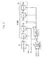
- FIG. 1 is a diagram of a conventional common clock control device configuration.
- the common clock control device includes a set circuit 10 and a shift register 20 .
- the set circuit 10 sets an input address Ai depending on a Column Address Strobe (CAS) signal CASP to provide an address AYi.
- the shift register 20 is provided with a plurality of D flip-flops DFF 1 to DFF 4 connected in series. The D flip-flops DFF 1 to DFF 4 sequentially perform a flip-flop operation of the address AYi in synchronism with an internal clock iCLK to output an address AYI_x.
- the conventional clock control device as configured above allows a signal input in synchronism with an external clock to be recognized in synchronism with the internal clock iCLK in a semiconductor memory that operates by a low frequency external clock.
- An interval between an input timing of a signal synchronization with the external clock and a recognition timing of the signal synchronization with the internal clock iCLK is defined as an internal latency.
- DDR3 SD AM Double Data Rate Synchronous Dynamic Random Access Memory
- a write command WT is input synchronously by the next clock CLK after an active command ACT and then data is input after a certain time delay. After the data input, a write operation is conducted in a core region of an actual DRAM.
- address data corresponding to the internal latency must be fed to recognize address data input upon input of the write command WT at the initial time of write operation in the core region of the actual DRAM.
- the address AYi is output by triggering an external input address Ai in response to the CAS signal CASP synchronized with the clock CLK upon input of the write command WT.
- the D flip-flops DFF 1 to DFF 4 sequentially conduct a flip-flop operation of the address AYi triggered in synchronism with the internal clock iCLK, thereby outputting the address AYI_x. That is, they sequentially conduct the flip-flop operation of the address AYi according to the CAS signal CASP_WT, enabled synchronously by the clock CLK at which the write operation is done in the core region of the DRAM.
- the general clock control device as structured above is operated by applying the internal clock iCLK to the D flip-flop DFF constantly, regardless of the current state of the chip. For the above reason, current consumption is increased as the internal clock iCLK is periodically transitioned.
- a primary object of the present invention to provide a technology capable of decreasing current consumption by toggling an internal clock in a precharge/standby state by controlling the clock to toggle only in an active state in a semiconductor memory that allows command signals and addresses externally input to be applied to a core after an internal latency.
- a clock control device including: a set circuit for triggering an input address in response to an internal command signal to output a first address; a shift register including a plurality of flip-flops connected in series, wherein some of the flip-flops perform a flip-flop operation of the first address in synchronism with an internal clock to provide a second address and the remaining flip-flops sequentially conduct a flip-flop operation of the second address in synchronism with a synchronous clock to produce an internal address; an active signal generator for outputting an active signal based on state of an active control signal indicating whether or not each bank is activated and a precharge control signal; and a clock generator for generating the synchronous clock depending on the internal clock and the active signal.
- a clock control device including: a set circuit for triggering an input address in response to an internal command signal to output a first address; a shift register including a plurality of flip-flops coupled in series, wherein some of the flip-flops conduct a flip-flop operation of the first address in synchronism with an internal clock to provide a second address and the remaining flip-flops sequentially perform a flip-flop operation of the second address in synchronism with a synchronous clock to produce an inner address; an active signal generator for outputting an active signal based on state of an active control signal indicating whether or not each bank is activated and a precharge control signal; a flip-flop for carrying out a flip-flop operation of the active signal in synchronism with the internal clock to provide a delayed active signal; and a clock generator for generating the synchronous clock depending on the internal clock and the delayed active signal.
- FIG. 1 is a block diagram of a configuration of a common clock control device
- FIG. 2 is an operational timing diagram of a common clock control device
- FIG. 3 is a block diagram illustrating a configuration of a clock control device in accordance with an embodiment of the present invention
- FIG. 4 is a detailed circuit diagram of the set circuit shown in FIG. 3 ;
- FIG. 5 is a detailed circuit diagram of the shift register shown in FIG. 3 ;
- FIG. 6 is a detailed circuit diagram of the active signal generator depicted in FIG. 3 ;
- FIG. 7 is a detailed circuit diagram of the clock generator shown in FIG. 3 ;
- FIG. 8 is an operational timing diagram of the clock generator in accordance with the embodiment of the present invention.
- FIG. 9 is a block diagram of a clock control device in accordance with another embodiment of the invention.
- FIG. 3 is a block diagram illustrating a configuration of a clock control device in accordance with the present invention.
- the clock control device of the invention comprises a set circuit 100 , a shift register 200 , an active signal generator 300 and a clock generator 400 .
- the set circuit 100 triggers an input address Ai in response to a CAS signal CASP to provide an address AYi.
- the shift register 200 includes a plurality of D flip-flops DFF 1 to DFF 4 coupled in series.
- the D flip-flop DFF 1 conducts a flip-flop operation of the address AYi in synchronism with an internal clock iCLK to output an address Ayi_a.
- the D flip-flop DFF 2 performs a flip-flop operation of an address Ayi_a in synchronism with the internal clock iCLK to provide an address Ayi_b.
- the D flip-flops DFF 3 and DFF 4 carry out a flip-flop operation of the internal address Ayi_b in synchronism with a synchronous clock SCLK to produce an internal address AYI_x.
- the active signal generator 300 generates an active signal RATVD based on an active signal ACTP ⁇ 0:i> and a precharge control signal PCGP ⁇ 0:i>, in which the active signal indicates that memory is in an active state.
- the clock generator 400 creates the synchronous clock SCLK depending on the internal clock iCLK and the active signal RATVD.
- FIG. 4 is a detailed circuit diagram of the set circuit 100 shown in FIG. 3 .
- the set circuit 100 is provided with a transmission gate T 1 and a multiplicity of inverters IV 1 to IV 5 .
- the transmission gate T 1 serves to selectively output the input address Ai on the basis of the CAS signal CASP and a CAS signal CASP inverted by the inverter IV 1 .
- the inverters IV 3 and IV 4 latch the output signal of the transmission gate T 1 for a preset time.
- the inverter IV 5 inverts the output of the latch composed of the inverters IV 3 and IV 4 to produce an internal address AYi.
- FIG. 5 presents a detailed circuit diagram of the shift register 200 shown in FIG. 3 .
- Each D flip-flop DFF includes transmission gates T 2 and T 3 and plural inverters IV 6 to IV 10 .
- the transmission gate T 2 selectively outputs the internal address AYi in response to the internal clock iCLK and an internal clock iCLK inverted by the inverter IV 6 .
- the inverters IV 7 and IV 8 latch the output signal of the transmission gate T 2 for a predetermined time.
- the transmission gate T 3 is operated contemporarily with the transmission gate T 2 based on the internal clock iCLK and the internal clock iCLK inverted by the inverter IV 6 to selectively control the output of the latch composed of the inverters IV 7 and IV 8 .
- a latch, composed of the inverters IV 9 and IV 10 latches the output of the transmission gate T 3 to provide an output signal OUT.
- FIG. 6 provides a detailed circuit diagram of the active signal generator 300 depicted in FIG. 3 .
- the active signal generator 300 includes a plurality of active controllers 310 to 330 and a logical operator 340 .
- Each of the active controllers 310 to 330 logically operates an active control signal ACTP ⁇ 0:i> and a precharge control signal PCGP ⁇ 0:i>, respectively.
- the plurality of active controllers 310 to 330 has the same configuration; and thus, only a controller 310 will be described below in detail.
- the active controller 310 is provided with an inverter IV 11 and NAND gates ND 1 and ND 2 .
- the NAND gate ND 1 does a NAND operation of an active control signal ACTP ⁇ 0> inverted by the inverter IV 11 and an output of the NAND gate ND 1 .
- NAND gate ND 2 performs a NAND operation of the precharge control signal PCGP ⁇ 0> and the output of the NAND gate ND 1 .
- the logical operator 340 includes a NOR gate NOR 1 and an inverter IV 12 .
- the NOR gate NOR 1 NOR-operates the outputs of the plurality of active controllers 310 to 330 .
- the inverter IV 12 inverts the output of the NOR gate NOR 1 to produce an active signal RATVD.
- FIG. 7 is a detailed circuit diagram of the clock generator 400 shown in FIG. 3 .
- the clock generator 400 is equipped with a NAND gate ND 3 and an inverter IV 13 .
- the NAND gate ND 3 acts a NAND operation of the internal clock iCLK and the active signal RATVD.
- the inverter IV 13 inverts the output of the NAND gate ND 3 to provide the synchronous clock SCLK.
- FIGS. 3 to 7 Operation of the invention as configured above will be explained in detail referring to FIGS. 3 to 7 in parallel with an operational timing diagram shown in FIG. 8 .
- the set circuit 100 latches the input address Ai input synchronously by a clock signal CLK upon activation of the CAS signal CASP to output the address AYi.
- the external input address Ai is sensed by the CAS signal CASP created by an internal command signal, write or read command.
- the shift register 200 conducts a flip-flop operation of the address AYi in synchronism with the internal clock iCLK to output the internal address Ayi_b and sequentially acts a flip-flop operation of the address Ayi_b in synchronism with the synchronous clock SCLK to provide the internal address AYI_x.
- the active signal generator 300 is provided with the plurality of active controllers 310 to 330 for controlling active status data of each of the banks.
- This active signal generator 300 logically operates each of the active signal ACTP ⁇ 0:i> and the precharge control signal PCGP ⁇ 0:i> to provide the active signal RATVD indicating that memory is in an active state. Therefore, the active signal RATVD is of logic low if all the banks are in a precharge state and is activated to logic high if any one of them is in an active state.
- the clock generator 400 generates the synchronous clock SCLK based on the clock signal RATVD and the internal clock iCLK. In other words, if the active signal RATVD is in an activation state, the synchronous clock SCLK is output synchronously by the internal clock iCLK.
- This invention controls the operation of the shift register 200 depending on both of the internal clock iCLK and the synchronous clock SCLK. That is, the active signal RATVD is activated by the active control signal ACTP denoting the external active command. Therefore, upon high speed operation, an internal delay time from a clock CLK at which the active control signal ACTP is input extends to a prolonged clock tA.
- the synchronous clock SCLK that is operated only when chip is in an active state is generated only after that time. If all the D flip-flops DFF 1 to DFF 4 of the shift register 200 are controlled by synchronizing with the synchronous clock SCLK, the first D flip-flop DFF 1 senses the internal address AYi that is the output of the set circuit 100 by the synchronous clock SCLK generated after the delayed time tA. In this case, the transfer of valid information becomes substantially slower than a time at which it should be resynchronized, thereby causing a malfunctioning.
- the invention controls the operation of the shift register 200 by separating the internal clock iCLK and the synchronous clock SCLK in order to assure the high speed operation.
- the delayed time tA is varied relying upon Process, Voltage and Temperature (PVT); and thus, the internal clock iCLK and the synchronous clock SCLK are distributed by considering circumstances by which the synchronous clock SCLK is produced after the delayed time.
- PVT Process, Voltage and Temperature
- the invention properly can properly control a clock excessively operated in the precharge state during the high speed operation, thereby decreasing current consumption (in SDRAM, average current consumption is defined by IDD 2 N) in the precharge state.
- FIG. 9 is a block diagram of a clock control device in accordance with another embodiment of the invention.
- the embodiment of FIG. 9 comprises a set circuit 100 , a shift register 200 , an active signal generator 300 , a clock generator 400 and a D flip-flop 500 .
- the embodiment of FIG. 9 as structured above further comprises a D flip-flop 500 , compared to the structure of FIG. 3 .
- the D flip-flop 500 performs a flip-flop operation of the active signal RATVD output from the active signal generator 300 to provide a delayed active signal RATVD.
- the synchronous clock SCLK can be created more stably by allowing the active signal RATVD applied to the clock generator 400 to be synchronized at a falling edge of the internal clock iCLK.
- the active signal RATVD is synchronized with the internal clock iCLK
- the active signal RATVD is a signal delayed by the internal delay
- the internal clock iCLK is an internal clock signal interworking depending on an external clock. Therefore, there may be a state where the internal clock iCLK becomes logic high at the time when the active signal RATVD is activated to logic high.
- the synchronous clock SCLK may be created as a glitch signal with incomplete pulse width.
- the embodiment of FIG. 9 can prevent the malfunctioning by the synchronous clock with glitch component by separating the D flip-flop 500 synchronized with the internal clock iCLK from the D flip-flop DFF of the shift register 200 synchronized with the synchronous clock SCLK.
- the input signal may be address, control signal, or data in the invention, without limiting thereto.
- the invention can decrease current consumption by toggling of an internal clock in a precharge/standby state by toggling it only in an active state in a semiconductor memory that allows command signals and addresses inputted from outside to be applied to a core after an internal latency.
- the present application contains subject matter related to Korean patent application No. 2005-91673 and No. 2005-117137, filed with the Korean Intellectual Property Office on Sep. 29, 2005 and on Dec. 02, 2005, the entire contents of which are incorporated herein by reference.
Abstract
Description
Claims (23)
Priority Applications (1)
| Application Number | Priority Date | Filing Date | Title |
|---|---|---|---|
| US13/369,988 USRE44590E1 (en) | 2005-09-29 | 2012-02-09 | Clock control device for toggling an internal clock of a synchronous DRAM for reduced power consumption |
Applications Claiming Priority (6)
| Application Number | Priority Date | Filing Date | Title |
|---|---|---|---|
| KR20050091673 | 2005-09-29 | ||
| KR10-2005-0091673 | 2005-09-29 | ||
| KR10-2005-0117137 | 2005-12-02 | ||
| KR1020050117137A KR100798766B1 (en) | 2005-09-29 | 2005-12-02 | Device for controlling clock |
| US11/476,597 US7307913B2 (en) | 2005-09-29 | 2006-06-29 | Clock control device for toggling an internal clock of a synchronous DRAM for reduced power consumption |
| US13/369,988 USRE44590E1 (en) | 2005-09-29 | 2012-02-09 | Clock control device for toggling an internal clock of a synchronous DRAM for reduced power consumption |
Related Parent Applications (1)
| Application Number | Title | Priority Date | Filing Date |
|---|---|---|---|
| US11/476,597 Reissue US7307913B2 (en) | 2005-09-29 | 2006-06-29 | Clock control device for toggling an internal clock of a synchronous DRAM for reduced power consumption |
Publications (1)
| Publication Number | Publication Date |
|---|---|
| USRE44590E1 true USRE44590E1 (en) | 2013-11-12 |
Family
ID=37893723
Family Applications (2)
| Application Number | Title | Priority Date | Filing Date |
|---|---|---|---|
| US11/476,597 Active US7307913B2 (en) | 2005-09-29 | 2006-06-29 | Clock control device for toggling an internal clock of a synchronous DRAM for reduced power consumption |
| US13/369,988 Active USRE44590E1 (en) | 2005-09-29 | 2012-02-09 | Clock control device for toggling an internal clock of a synchronous DRAM for reduced power consumption |
Family Applications Before (1)
| Application Number | Title | Priority Date | Filing Date |
|---|---|---|---|
| US11/476,597 Active US7307913B2 (en) | 2005-09-29 | 2006-06-29 | Clock control device for toggling an internal clock of a synchronous DRAM for reduced power consumption |
Country Status (1)
| Country | Link |
|---|---|
| US (2) | US7307913B2 (en) |
Families Citing this family (1)
| Publication number | Priority date | Publication date | Assignee | Title |
|---|---|---|---|---|
| US7307913B2 (en) * | 2005-09-29 | 2007-12-11 | Hynix Semiconductor Inc. | Clock control device for toggling an internal clock of a synchronous DRAM for reduced power consumption |
Citations (14)
| Publication number | Priority date | Publication date | Assignee | Title |
|---|---|---|---|---|
| US5835956A (en) | 1899-10-02 | 1998-11-10 | Samsung Electronics Co., Ltd. | Synchronous dram having a plurality of latency modes |
| JP2000090666A (en) | 1998-08-27 | 2000-03-31 | Samsung Electronics Co Ltd | Internal clock signal generation circuit and synchronization type dram device |
| US6101144A (en) | 1998-05-25 | 2000-08-08 | Samsung Electronics Co., Ltd. | Integrated circuit memory devices having automatically induced standby modes and methods of operating same |
| US6154415A (en) | 1997-02-17 | 2000-11-28 | Samsung Electronics, Co., Ltd. | Internal clock generation circuit of semiconductor device and method for generating internal clock |
| US6243320B1 (en) * | 1998-07-29 | 2001-06-05 | Mitsubishi Denki Kabushiki Kaisha | Synchronous semiconductor memory device capable of selecting column at high speed |
| US6330200B2 (en) * | 1998-06-17 | 2001-12-11 | Mitsubishi Denki Kabushiki Kaisha | Synchronous semiconductor memory device having improved operational frequency margin at data input/output |
| US6366515B2 (en) * | 2000-06-21 | 2002-04-02 | Mitsubishi Denki Kabushiki Kaisha | Semiconductor memory device |
| US20020039326A1 (en) | 2000-09-28 | 2002-04-04 | Kabushiki Kaisha Toshiba | Clock synchronous circuit |
| US6552959B2 (en) | 2001-06-18 | 2003-04-22 | Mitsubishi Denki Kabushiki Kaisha | Semiconductor memory device operable for both of CAS latencies of one and more than one |
| US6738309B2 (en) | 2001-05-23 | 2004-05-18 | Infineon Technologies Ag | Semiconductor memory and method for operating the semiconductor memory |
| US20040168134A1 (en) | 2003-02-21 | 2004-08-26 | Infineon Technologies North America Corp. | Clock gating approach to accommodate infrequent additional processing latencies |
| US20050234205A1 (en) | 2002-06-13 | 2005-10-20 | Fumihiko Yamaguchi | Copolymer, paper-treating agent, and processed paper |
| US7102939B2 (en) | 2003-10-14 | 2006-09-05 | Hynix Semiconductor, Inc. | Semiconductor memory device having column address path therein for reducing power consumption |
| US20070070791A1 (en) * | 2005-09-29 | 2007-03-29 | Hynix Semiconductor Inc. | Clock control device |
-
2006
- 2006-06-29 US US11/476,597 patent/US7307913B2/en active Active
-
2012
- 2012-02-09 US US13/369,988 patent/USRE44590E1/en active Active
Patent Citations (16)
| Publication number | Priority date | Publication date | Assignee | Title |
|---|---|---|---|---|
| US5835956A (en) | 1899-10-02 | 1998-11-10 | Samsung Electronics Co., Ltd. | Synchronous dram having a plurality of latency modes |
| US6154415A (en) | 1997-02-17 | 2000-11-28 | Samsung Electronics, Co., Ltd. | Internal clock generation circuit of semiconductor device and method for generating internal clock |
| US6101144A (en) | 1998-05-25 | 2000-08-08 | Samsung Electronics Co., Ltd. | Integrated circuit memory devices having automatically induced standby modes and methods of operating same |
| US6330200B2 (en) * | 1998-06-17 | 2001-12-11 | Mitsubishi Denki Kabushiki Kaisha | Synchronous semiconductor memory device having improved operational frequency margin at data input/output |
| US6243320B1 (en) * | 1998-07-29 | 2001-06-05 | Mitsubishi Denki Kabushiki Kaisha | Synchronous semiconductor memory device capable of selecting column at high speed |
| US6333892B2 (en) * | 1998-07-29 | 2001-12-25 | Mitsubishi Denki Kabushiki Kaisha | Synchronous semiconductor memory device capable of selecting column at high speed |
| JP2000090666A (en) | 1998-08-27 | 2000-03-31 | Samsung Electronics Co Ltd | Internal clock signal generation circuit and synchronization type dram device |
| US6366515B2 (en) * | 2000-06-21 | 2002-04-02 | Mitsubishi Denki Kabushiki Kaisha | Semiconductor memory device |
| US20020039326A1 (en) | 2000-09-28 | 2002-04-04 | Kabushiki Kaisha Toshiba | Clock synchronous circuit |
| US6738309B2 (en) | 2001-05-23 | 2004-05-18 | Infineon Technologies Ag | Semiconductor memory and method for operating the semiconductor memory |
| US6552959B2 (en) | 2001-06-18 | 2003-04-22 | Mitsubishi Denki Kabushiki Kaisha | Semiconductor memory device operable for both of CAS latencies of one and more than one |
| US20050234205A1 (en) | 2002-06-13 | 2005-10-20 | Fumihiko Yamaguchi | Copolymer, paper-treating agent, and processed paper |
| US20040168134A1 (en) | 2003-02-21 | 2004-08-26 | Infineon Technologies North America Corp. | Clock gating approach to accommodate infrequent additional processing latencies |
| US7102939B2 (en) | 2003-10-14 | 2006-09-05 | Hynix Semiconductor, Inc. | Semiconductor memory device having column address path therein for reducing power consumption |
| US20070070791A1 (en) * | 2005-09-29 | 2007-03-29 | Hynix Semiconductor Inc. | Clock control device |
| US7307913B2 (en) * | 2005-09-29 | 2007-12-11 | Hynix Semiconductor Inc. | Clock control device for toggling an internal clock of a synchronous DRAM for reduced power consumption |
Also Published As
| Publication number | Publication date |
|---|---|
| US7307913B2 (en) | 2007-12-11 |
| US20070070791A1 (en) | 2007-03-29 |
Similar Documents
| Publication | Publication Date | Title |
|---|---|---|
| US7196966B2 (en) | On die termination mode transfer circuit in semiconductor memory device and its method | |
| KR100422572B1 (en) | Register controlled delay locked loop and semiconductor device having the same | |
| US7280430B2 (en) | Semiconductor memory device | |
| US7693000B2 (en) | Semiconductor device | |
| US7911862B2 (en) | Latency control circuit and method thereof and an auto-precharge control circuit and method thereof | |
| US20060274592A1 (en) | Circuit and method for controlling a clock synchronizing circuit for low power refresh operation | |
| US7227794B2 (en) | Internal voltage generation control circuit and internal voltage generation circuit using the same | |
| US20090238021A1 (en) | Semiconductor memory device and operation method therefor | |
| US6795363B2 (en) | Refresh control method of semiconductor memory device and semiconductor memory device comprising the same control method | |
| KR20060075060A (en) | Clock generation apparatus in semiconductor memory device and its method | |
| US7522467B2 (en) | Semiconductor memory device | |
| JP3689229B2 (en) | Column selection line enable circuit for semiconductor memory device | |
| JP2907081B2 (en) | Semiconductor storage device | |
| US20030223279A1 (en) | Clock driver in semiconductor memory device | |
| USRE44590E1 (en) | Clock control device for toggling an internal clock of a synchronous DRAM for reduced power consumption | |
| KR100798766B1 (en) | Device for controlling clock | |
| KR100296920B1 (en) | Circuit for controlling write mode in semiconductor memory device | |
| KR20030050181A (en) | Semiconductor memory device | |
| US7741892B2 (en) | Data output controller | |
| US7751271B2 (en) | Semiconductor memory device | |
| KR100909625B1 (en) | Address synchronization circuit | |
| KR100665847B1 (en) | Semiconductor memory device having precharge control circuit and method for precharge therefore | |
| US7952957B2 (en) | Circuit for generating read and signal and circuit for generating internal clock using the same | |
| JP2007128646A (en) | Semiconductor memory device | |
| KR100557970B1 (en) | I / O buffer |
Legal Events
| Date | Code | Title | Description |
|---|---|---|---|
| AS | Assignment |
Owner name: CONVERSANT IP N.B. 868 INC., CANADA Free format text: CHANGE OF NAME;ASSIGNOR:658868 N.B. INC.;REEL/FRAME:032439/0547 Effective date: 20140101 |
|
| AS | Assignment |
Owner name: CPPIB CREDIT INVESTMENTS INC., AS LENDER, CANADA Free format text: U.S. PATENT SECURITY AGREEMENT (FOR NON-U.S. GRANTORS);ASSIGNOR:CONVERSANT IP N.B. 868 INC.;REEL/FRAME:033707/0001 Effective date: 20140611 Owner name: ROYAL BANK OF CANADA, AS LENDER, CANADA Free format text: U.S. PATENT SECURITY AGREEMENT (FOR NON-U.S. GRANTORS);ASSIGNOR:CONVERSANT IP N.B. 868 INC.;REEL/FRAME:033707/0001 Effective date: 20140611 |
|
| FPAY | Fee payment |
Year of fee payment: 8 |
|
| AS | Assignment |
Owner name: CONVERSANT INTELLECTUAL PROPERTY MANAGEMENT INC., Free format text: ASSIGNMENT OF ASSIGNORS INTEREST;ASSIGNOR:CONVERSANT IP N.B. 868 INC.;REEL/FRAME:036159/0386 Effective date: 20150514 |
|
| AS | Assignment |
Owner name: CPPIB CREDIT INVESTMENTS, INC., CANADA Free format text: AMENDED AND RESTATED U.S. PATENT SECURITY AGREEMENT (FOR NON-U.S. GRANTORS);ASSIGNOR:CONVERSANT INTELLECTUAL PROPERTY MANAGEMENT INC.;REEL/FRAME:046900/0136 Effective date: 20180731 |
|
| AS | Assignment |
Owner name: CONVERSANT INTELLECTUAL PROPERTY MANAGEMENT INC., CANADA Free format text: RELEASE OF U.S. PATENT AGREEMENT (FOR NON-U.S. GRANTORS);ASSIGNOR:ROYAL BANK OF CANADA, AS LENDER;REEL/FRAME:047645/0424 Effective date: 20180731 Owner name: CONVERSANT INTELLECTUAL PROPERTY MANAGEMENT INC., Free format text: RELEASE OF U.S. PATENT AGREEMENT (FOR NON-U.S. GRANTORS);ASSIGNOR:ROYAL BANK OF CANADA, AS LENDER;REEL/FRAME:047645/0424 Effective date: 20180731 |
|
| MAFP | Maintenance fee payment |
Free format text: PAYMENT OF MAINTENANCE FEE, 12TH YEAR, LARGE ENTITY (ORIGINAL EVENT CODE: M1553); ENTITY STATUS OF PATENT OWNER: LARGE ENTITY Year of fee payment: 12 |
|
| AS | Assignment |
Owner name: CONVERSANT INTELLECTUAL PROPERTY MANAGEMENT INC., CANADA Free format text: RELEASE BY SECURED PARTY;ASSIGNOR:CPPIB CREDIT INVESTMENTS INC.;REEL/FRAME:054371/0684 Effective date: 20201028 |
|
| AS | Assignment |
Owner name: MOSAID TECHNOLOGIES INCORPORATED, CANADA Free format text: CHANGE OF NAME;ASSIGNOR:CONVERSANT INTELLECTUAL PROPERTY INC.;REEL/FRAME:058297/0853 Effective date: 20210401 |
|
| AS | Assignment |
Owner name: MOSAID TECHNOLOGIES INCORPORATED, CANADA Free format text: CORRECTIVE ASSIGNMENT TO CORRECT THE CONVEYING PARTY'S NAME PREVIOUSLY RECORDED ON REEL 058297 FRAME 0853. ASSIGNOR(S) HEREBY CONFIRMS THE CHANGE OF NAME;ASSIGNOR:CONVERSANT INTELLECTUAL PROPERTY MANAGEMENT INC.;REEL/FRAME:064742/0953 Effective date: 20210401 |