KR100807606B1 - 광학 보상층 부착 편광판, 액정 패널, 액정 표시 장치,화상 표시 장치 및 광학 보상층 부착 편광판의 제조 방법 - Google Patents
광학 보상층 부착 편광판, 액정 패널, 액정 표시 장치,화상 표시 장치 및 광학 보상층 부착 편광판의 제조 방법 Download PDFInfo
- Publication number
- KR100807606B1 KR100807606B1 KR1020077004537A KR20077004537A KR100807606B1 KR 100807606 B1 KR100807606 B1 KR 100807606B1 KR 1020077004537 A KR1020077004537 A KR 1020077004537A KR 20077004537 A KR20077004537 A KR 20077004537A KR 100807606 B1 KR100807606 B1 KR 100807606B1
- Authority
- KR
- South Korea
- Prior art keywords
- optical compensation
- compensation layer
- polarizing plate
- liquid crystal
- film
- Prior art date
Links
Images


Classifications
-
- G—PHYSICS
- G02—OPTICS
- G02B—OPTICAL ELEMENTS, SYSTEMS OR APPARATUS
- G02B5/00—Optical elements other than lenses
- G02B5/30—Polarising elements
-
- G—PHYSICS
- G02—OPTICS
- G02F—OPTICAL DEVICES OR ARRANGEMENTS FOR THE CONTROL OF LIGHT BY MODIFICATION OF THE OPTICAL PROPERTIES OF THE MEDIA OF THE ELEMENTS INVOLVED THEREIN; NON-LINEAR OPTICS; FREQUENCY-CHANGING OF LIGHT; OPTICAL LOGIC ELEMENTS; OPTICAL ANALOGUE/DIGITAL CONVERTERS
- G02F1/00—Devices or arrangements for the control of the intensity, colour, phase, polarisation or direction of light arriving from an independent light source, e.g. switching, gating or modulating; Non-linear optics
- G02F1/01—Devices or arrangements for the control of the intensity, colour, phase, polarisation or direction of light arriving from an independent light source, e.g. switching, gating or modulating; Non-linear optics for the control of the intensity, phase, polarisation or colour
- G02F1/13—Devices or arrangements for the control of the intensity, colour, phase, polarisation or direction of light arriving from an independent light source, e.g. switching, gating or modulating; Non-linear optics for the control of the intensity, phase, polarisation or colour based on liquid crystals, e.g. single liquid crystal display cells
- G02F1/133—Constructional arrangements; Operation of liquid crystal cells; Circuit arrangements
- G02F1/1333—Constructional arrangements; Manufacturing methods
- G02F1/1335—Structural association of cells with optical devices, e.g. polarisers or reflectors
- G02F1/13363—Birefringent elements, e.g. for optical compensation
-
- G—PHYSICS
- G02—OPTICS
- G02B—OPTICAL ELEMENTS, SYSTEMS OR APPARATUS
- G02B5/00—Optical elements other than lenses
- G02B5/30—Polarising elements
- G02B5/3025—Polarisers, i.e. arrangements capable of producing a definite output polarisation state from an unpolarised input state
- G02B5/3033—Polarisers, i.e. arrangements capable of producing a definite output polarisation state from an unpolarised input state in the form of a thin sheet or foil, e.g. Polaroid
-
- G—PHYSICS
- G02—OPTICS
- G02F—OPTICAL DEVICES OR ARRANGEMENTS FOR THE CONTROL OF LIGHT BY MODIFICATION OF THE OPTICAL PROPERTIES OF THE MEDIA OF THE ELEMENTS INVOLVED THEREIN; NON-LINEAR OPTICS; FREQUENCY-CHANGING OF LIGHT; OPTICAL LOGIC ELEMENTS; OPTICAL ANALOGUE/DIGITAL CONVERTERS
- G02F1/00—Devices or arrangements for the control of the intensity, colour, phase, polarisation or direction of light arriving from an independent light source, e.g. switching, gating or modulating; Non-linear optics
- G02F1/01—Devices or arrangements for the control of the intensity, colour, phase, polarisation or direction of light arriving from an independent light source, e.g. switching, gating or modulating; Non-linear optics for the control of the intensity, phase, polarisation or colour
- G02F1/13—Devices or arrangements for the control of the intensity, colour, phase, polarisation or direction of light arriving from an independent light source, e.g. switching, gating or modulating; Non-linear optics for the control of the intensity, phase, polarisation or colour based on liquid crystals, e.g. single liquid crystal display cells
- G02F1/133—Constructional arrangements; Operation of liquid crystal cells; Circuit arrangements
- G02F1/1333—Constructional arrangements; Manufacturing methods
- G02F1/1335—Structural association of cells with optical devices, e.g. polarisers or reflectors
- G02F1/133528—Polarisers
- G02F1/133531—Polarisers characterised by the arrangement of polariser or analyser axes
-
- G—PHYSICS
- G02—OPTICS
- G02F—OPTICAL DEVICES OR ARRANGEMENTS FOR THE CONTROL OF LIGHT BY MODIFICATION OF THE OPTICAL PROPERTIES OF THE MEDIA OF THE ELEMENTS INVOLVED THEREIN; NON-LINEAR OPTICS; FREQUENCY-CHANGING OF LIGHT; OPTICAL LOGIC ELEMENTS; OPTICAL ANALOGUE/DIGITAL CONVERTERS
- G02F2202/00—Materials and properties
- G02F2202/40—Materials having a particular birefringence, retardation
-
- G—PHYSICS
- G02—OPTICS
- G02F—OPTICAL DEVICES OR ARRANGEMENTS FOR THE CONTROL OF LIGHT BY MODIFICATION OF THE OPTICAL PROPERTIES OF THE MEDIA OF THE ELEMENTS INVOLVED THEREIN; NON-LINEAR OPTICS; FREQUENCY-CHANGING OF LIGHT; OPTICAL LOGIC ELEMENTS; OPTICAL ANALOGUE/DIGITAL CONVERTERS
- G02F2413/00—Indexing scheme related to G02F1/13363, i.e. to birefringent elements, e.g. for optical compensation, characterised by the number, position, orientation or value of the compensation plates
- G02F2413/02—Number of plates being 2
-
- G—PHYSICS
- G02—OPTICS
- G02F—OPTICAL DEVICES OR ARRANGEMENTS FOR THE CONTROL OF LIGHT BY MODIFICATION OF THE OPTICAL PROPERTIES OF THE MEDIA OF THE ELEMENTS INVOLVED THEREIN; NON-LINEAR OPTICS; FREQUENCY-CHANGING OF LIGHT; OPTICAL LOGIC ELEMENTS; OPTICAL ANALOGUE/DIGITAL CONVERTERS
- G02F2413/00—Indexing scheme related to G02F1/13363, i.e. to birefringent elements, e.g. for optical compensation, characterised by the number, position, orientation or value of the compensation plates
- G02F2413/07—All plates on one side of the LC cell
-
- G—PHYSICS
- G02—OPTICS
- G02F—OPTICAL DEVICES OR ARRANGEMENTS FOR THE CONTROL OF LIGHT BY MODIFICATION OF THE OPTICAL PROPERTIES OF THE MEDIA OF THE ELEMENTS INVOLVED THEREIN; NON-LINEAR OPTICS; FREQUENCY-CHANGING OF LIGHT; OPTICAL LOGIC ELEMENTS; OPTICAL ANALOGUE/DIGITAL CONVERTERS
- G02F2413/00—Indexing scheme related to G02F1/13363, i.e. to birefringent elements, e.g. for optical compensation, characterised by the number, position, orientation or value of the compensation plates
- G02F2413/08—Indexing scheme related to G02F1/13363, i.e. to birefringent elements, e.g. for optical compensation, characterised by the number, position, orientation or value of the compensation plates with a particular optical axis orientation
-
- G—PHYSICS
- G02—OPTICS
- G02F—OPTICAL DEVICES OR ARRANGEMENTS FOR THE CONTROL OF LIGHT BY MODIFICATION OF THE OPTICAL PROPERTIES OF THE MEDIA OF THE ELEMENTS INVOLVED THEREIN; NON-LINEAR OPTICS; FREQUENCY-CHANGING OF LIGHT; OPTICAL LOGIC ELEMENTS; OPTICAL ANALOGUE/DIGITAL CONVERTERS
- G02F2413/00—Indexing scheme related to G02F1/13363, i.e. to birefringent elements, e.g. for optical compensation, characterised by the number, position, orientation or value of the compensation plates
- G02F2413/12—Biaxial compensators
-
- G—PHYSICS
- G02—OPTICS
- G02F—OPTICAL DEVICES OR ARRANGEMENTS FOR THE CONTROL OF LIGHT BY MODIFICATION OF THE OPTICAL PROPERTIES OF THE MEDIA OF THE ELEMENTS INVOLVED THEREIN; NON-LINEAR OPTICS; FREQUENCY-CHANGING OF LIGHT; OPTICAL LOGIC ELEMENTS; OPTICAL ANALOGUE/DIGITAL CONVERTERS
- G02F2413/00—Indexing scheme related to G02F1/13363, i.e. to birefringent elements, e.g. for optical compensation, characterised by the number, position, orientation or value of the compensation plates
- G02F2413/13—Positive birefingence
Landscapes
- Physics & Mathematics (AREA)
- Nonlinear Science (AREA)
- General Physics & Mathematics (AREA)
- Optics & Photonics (AREA)
- Mathematical Physics (AREA)
- Chemical & Material Sciences (AREA)
- Crystallography & Structural Chemistry (AREA)
- Polarising Elements (AREA)
- Liquid Crystal (AREA)
Abstract
Description
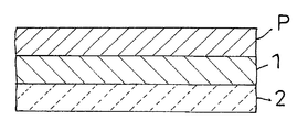
또한, 상기 편광판의 흡수축에 대하여 상기 광학 보상층 (1) 의 지상축이 이루는 각도는 반시계 방향으로 10∼30°의 범위이고, 상기 편광판의 흡수축에 대하여 상기 광학 보상층 (2) 의 지상축이 이루는 각도는 반시계 방향으로 75∼95°의 범위이고,
롤형의 상기 편광판과 롤형의 상기 광학 보상층 (2) 을, 상기 편광판의 흡수축에 대하여 상기 광학 보상층 (2) 의 지상축이 이루는 각도가 반시계 방향으로 75∼95°인 범위에서 쌍방의 긴 변 방향이 정렬되도록 연속 반송하는 공정,
상기 연속 반송되고 있는 상기 편광판과 상기 광학 보상층 (2) 사이에 상기 광학 보상층 (1) 을, 상기 지상축이 상기 편광판의 흡수축에 대하여 반시계 방향으로 10∼30°의 범위가 되도록 삽입하는 공정, 그리고,


Claims (13)
- 편광판, 광학 보상층 (1), 광학 보상층 (2) 이 이 순서로 적층된 광학 보상층 부착 편광판으로서,상기 광학 보상층 (1) 은, 필름면 내의 굴절률이 최대가 되는 방향을 X 축, X 축에 수직인 방향을 Y 축, 상기 필름의 두께 방향을 Z 축으로 하고, 각각의 축방향의 굴절률을 nx1, ny1, nz1 로 하고, 상기 필름 두께를 d1(㎚) 로 한 경우에,nx1>ny1=nz1 의 관계를 가지며,광탄성 계수의 절대값이 2.0×10⁻¹¹㎡/N 이하인 수지를 함유하며,정면 위상차 : (nx1-ny1)·d1=200∼300㎚ 의 범위이며,상기 광학 보상층 (2) 은, 상기 필름면 내의 굴절률이 최대가 되는 방향을 X 축, X 축에 수직인 방향을 Y 축, 상기 필름의 두께 방향을 Z 축으로 하고, 각각의 축방향의 굴절률을 nx2, ny2, nz2 로 한 경우에, 상기 필름 두께를 d2(㎚) 로 한 경우에,nx2>ny2>nz2 의 관계를 가지며,광탄성 계수의 절대값이 2.0×10⁻¹¹㎡/N 이하인 수지를 함유하며,정면 위상차 : (nx2-ny2)·d2=90∼160㎚ 의 범위이며,또한, 상기 편광판의 흡수축에 대하여 상기 광학 보상층 (1) 의 지상축이 이루는 각도는 반시계 방향으로 10∼30°의 범위이고, 상기 편광판의 흡수축에 대하여 상기 광학 보상층 (2) 의 지상축이 이루는 각도는 반시계 방향으로 75∼95°의 범위이고,상기 광학 보상층 부착 편광판은, VA 모드의 액정 셀에 적용되는 것을 특징으로 하는 광학 보상층 부착 편광판.
- 제 1 항에 있어서,상기 광학 보상층 (2) 은, Nz=(nx2-nz2)/(nx2-ny2) 로 표시되는 Nz 계수가 1.3∼1.9 의 범위인 것을 특징으로 하는 광학 보상층 부착 편광판.
- 제 1 항에 있어서,상기 광학 보상층 (1) 이, 노르보르넨계 수지를 함유하는 고분자 필름을 1 축 연신하여 얻을 수 있는 광학 필름인 것을 특징으로 하는 광학 보상층 부착 편광판.
- 제 1 항에 있어서,상기 광학 보상층 (2) 이, 노르보르넨계 수지를 함유하는 고분자 필름을 2 축 연신하여 얻을 수 있는 광학 필름인 것을 특징으로 하는 광학 보상층 부착 편광판.
- 제 1 항에 있어서,상기 편광판, 상기 광학 보상층 (1) 및 상기 광학 보상층 (2) 은 점착제에 의해 적층되어 있는 것을 특징으로 하는 광학 보상층 부착 편광판.
- 제 1 항 내지 제 5 항 중 어느 한 항에 기재된 광학 보상층 부착 편광판 및 VA 모드의 액정 셀을 포함하는 것을 특징으로 하는 액정 패널.
- 제 6 항에 기재된 액정 패널을 포함하는 것을 특징으로 하는 액정 표시 장치.
- 삭제
- 제 1 항 내지 제 5 항 중 어느 한 항에 기재된 VA 모드의 액정 셀에 적용되는 광학 보상층 부착 편광판의 제조 방법으로서,롤형의 상기 편광판과 롤형의 상기 광학 보상층 (2) 을, 상기 편광판의 흡수축에 대하여 상기 광학 보상층 (2) 의 지상축이 이루는 각도가 반시계 방향으로 75∼95°인 범위에서 쌍방의 긴 변 방향이 정렬되도록 연속 반송하는 공정,상기 연속 반송되고 있는 상기 편광판과 상기 광학 보상층 (2) 사이에 상기 광학 보상층 (1) 을, 상기 지상축이 상기 편광판의 흡수축에 대하여 반시계 방향으로 10∼30°의 범위가 되도록 삽입하는 공정, 그리고,상기 편광판, 상기 광학 보상층 (1) 및 상기 광학 보상층 (2) 을 적층하는 공정을 포함하는 것을 특징으로 하는 VA 모드의 액정 셀에 적용되는 광학 보상층 부착 편광판의 제조 방법.
- 삭제
- 삭제
- 삭제
- 삭제
Applications Claiming Priority (2)
| Application Number | Priority Date | Filing Date | Title |
|---|---|---|---|
| JPJP-P-2004-00337276 | 2004-11-22 | ||
| JP2004337276 | 2004-11-22 |
Publications (2)
| Publication Number | Publication Date |
|---|---|
| KR20070052284A KR20070052284A (ko) | 2007-05-21 |
| KR100807606B1 true KR100807606B1 (ko) | 2008-02-28 |
Family
ID=36407138
Family Applications (1)
| Application Number | Title | Priority Date | Filing Date |
|---|---|---|---|
| KR1020077004537A KR100807606B1 (ko) | 2004-11-22 | 2005-11-16 | 광학 보상층 부착 편광판, 액정 패널, 액정 표시 장치,화상 표시 장치 및 광학 보상층 부착 편광판의 제조 방법 |
Country Status (8)
| Country | Link |
|---|---|
| US (1) | US7852561B2 (ko) |
| EP (1) | EP1816496B1 (ko) |
| JP (1) | JP3874200B2 (ko) |
| KR (1) | KR100807606B1 (ko) |
| CN (1) | CN100472253C (ko) |
| PL (1) | PL1816496T3 (ko) |
| TW (1) | TW200624960A (ko) |
| WO (1) | WO2006054597A1 (ko) |
Cited By (1)
| Publication number | Priority date | Publication date | Assignee | Title |
|---|---|---|---|---|
| US9921351B2 (en) | 2012-05-10 | 2018-03-20 | Samsung Electronics Co., Ltd. | Multilayered optical film, manufacturing method thereof, and display device |
Families Citing this family (32)
| Publication number | Priority date | Publication date | Assignee | Title |
|---|---|---|---|---|
| JP2007155970A (ja) * | 2005-12-02 | 2007-06-21 | Sumitomo Chemical Co Ltd | 楕円偏光板及びその製造方法 |
| WO2009025360A1 (ja) * | 2007-08-22 | 2009-02-26 | Sumitomo Chemical Company, Limited | 複合偏光板、積層光学部材及びそれらを用いた画像表示装置 |
| JP2009151100A (ja) * | 2007-12-20 | 2009-07-09 | Sumitomo Chemical Co Ltd | 複合偏光板セットおよび液晶表示装置 |
| JP2009276753A (ja) * | 2008-04-14 | 2009-11-26 | Sumitomo Chemical Co Ltd | 位相差フィルム、楕円偏光板、液晶表示装置、および楕円偏光板の製造方法 |
| JP5301927B2 (ja) * | 2008-09-01 | 2013-09-25 | スタンレー電気株式会社 | 液晶表示素子 |
| KR101314480B1 (ko) | 2008-12-26 | 2013-10-07 | 주식회사 엘지화학 | 면상 스위치 모드 lcd용 편광판 및 이를 포함하는 면상 스위치 모드 lcd |
| JP4820443B2 (ja) * | 2009-11-20 | 2011-11-24 | 日東電工株式会社 | 光学フィルム用粘着剤組成物、光学フィルム用粘着剤層、粘着型光学フィルムおよび画像表示装置 |
| JP5661478B2 (ja) * | 2010-01-08 | 2015-01-28 | 日東電工株式会社 | 積層光学フィルムの製造方法 |
| ES2689402T3 (es) | 2011-04-15 | 2018-11-13 | Safilo S.P.A. | Método para realizar lentes curvas |
| ES2730977T3 (es) * | 2011-04-15 | 2019-11-13 | Safilo Spa | Lentes curvadas y procedimientos relacionados |
| WO2012140503A2 (en) | 2011-04-15 | 2012-10-18 | Polaroid Eyewear A Division Of Stylemark Uk, Ltd. | Curved lenses and related methods |
| JP5905761B2 (ja) | 2011-05-20 | 2016-04-20 | 日東電工株式会社 | 光学表示パネルの連続製造方法および光学表示パネルの連続製造システム |
| JP5945143B2 (ja) * | 2011-05-20 | 2016-07-05 | 日東電工株式会社 | 光学フィルムロールセットおよび光学フィルムロールセットの製造方法。 |
| KR101916948B1 (ko) * | 2011-12-12 | 2018-11-08 | 엘지디스플레이 주식회사 | 표시장치 |
| JP6549348B2 (ja) | 2012-11-06 | 2019-07-24 | 三星電子株式会社Samsung Electronics Co.,Ltd. | 偏光フィルム、反射防止フィルムおよび表示装置 |
| KR102223121B1 (ko) * | 2013-08-09 | 2021-03-05 | 스미또모 가가꾸 가부시키가이샤 | 장척 위상차 필름의 제조 방법 |
| KR102329698B1 (ko) * | 2013-08-09 | 2021-11-23 | 스미또모 가가꾸 가부시키가이샤 | 장척 원편광판의 제조 방법 및 장척 원편광판 |
| WO2015030176A1 (ja) * | 2013-08-30 | 2015-03-05 | 富士フイルム株式会社 | 応力表示部材および応力表示部材を用いたひずみ測定方法 |
| KR102079557B1 (ko) * | 2013-11-19 | 2020-02-20 | 엘지디스플레이 주식회사 | 유기발광소자용 편광판 및 이를 포함하는 유기발광소자 |
| WO2015101335A1 (zh) * | 2013-12-31 | 2015-07-09 | 昆山工研院新型平板显示技术中心有限公司 | 一种有机发光显示器件和改善视角特性的顶发射oled器件 |
| US9766384B2 (en) | 2014-12-08 | 2017-09-19 | Samsung Electronics Co., Ltd. | Antireflection film and organic light emitting device provided with the same |
| KR101623086B1 (ko) | 2014-12-08 | 2016-05-20 | 삼성전자 주식회사 | 반사방지필름 및 이를 구비한 유기발광장치 |
| JP2016118782A (ja) | 2014-12-17 | 2016-06-30 | 三星電子株式会社Samsung Electronics Co., Ltd. | 偏光フィルムおよびこれを含む表示装置 |
| KR20160079687A (ko) * | 2014-12-26 | 2016-07-06 | 삼성전자주식회사 | 반사방지필름 및 이를 구비한 유기발광장치 |
| KR102304889B1 (ko) | 2015-02-11 | 2021-09-23 | 삼성전자주식회사 | 유기 발광 장치 및 그 제조 방법 |
| JP6483811B2 (ja) * | 2015-04-13 | 2019-03-13 | 富士フイルム株式会社 | 透明基材フィルム積層体、タッチパネル用センサーフィルム、タッチパネル、画像表示装置および画像表示装置の視認性改善方法 |
| JPWO2017150375A1 (ja) * | 2016-02-29 | 2018-12-20 | 日本ゼオン株式会社 | 画像表示装置 |
| CN107193072B (zh) * | 2016-03-15 | 2018-08-28 | 住友化学株式会社 | 椭圆偏振板 |
| JP6359048B2 (ja) * | 2016-03-31 | 2018-07-18 | 住友化学株式会社 | 偏光フィルムの製造方法 |
| JP6257680B2 (ja) * | 2016-03-31 | 2018-01-10 | 住友化学株式会社 | 偏光フィルムの製造方法、積層フィルム |
| CN109466961B (zh) * | 2018-12-26 | 2023-09-29 | 郴州市海利微电子科技有限公司 | 偏光片模冲机的自动收片装置 |
| KR20210117391A (ko) * | 2020-03-18 | 2021-09-29 | 삼성디스플레이 주식회사 | 표시 장치 |
Citations (2)
| Publication number | Priority date | Publication date | Assignee | Title |
|---|---|---|---|---|
| JPH07253573A (ja) * | 1994-03-15 | 1995-10-03 | Matsushita Electric Ind Co Ltd | 液晶表示素子 |
| JP2003114325A (ja) * | 2001-10-03 | 2003-04-18 | Nitto Denko Corp | 積層1/4波長板、円偏光板及びこれを用いた液晶表示装置、ならびにその製造方法 |
Family Cites Families (11)
| Publication number | Priority date | Publication date | Assignee | Title |
|---|---|---|---|---|
| JPH1068816A (ja) * | 1996-08-29 | 1998-03-10 | Sharp Corp | 位相差板及び円偏光板 |
| DE03017342T1 (de) * | 1997-04-23 | 2004-08-26 | Sharp K.K. | Reflektierende Flüssigkristallanzeige |
| US6281952B1 (en) | 1997-12-26 | 2001-08-28 | Sharp Kabushiki Kaisha | Liquid crystal display |
| KR100623984B1 (ko) | 1999-12-02 | 2006-09-13 | 삼성전자주식회사 | 광시야각 액정 표시 장치 및 그에 사용되는 기판 |
| JP2001013500A (ja) * | 1999-06-30 | 2001-01-19 | Matsushita Electric Ind Co Ltd | 反射型液晶表示素子 |
| JP2001091745A (ja) * | 1999-09-22 | 2001-04-06 | Nitto Denko Corp | 複合位相差板、光学補償偏光板及び液晶表示装置 |
| JP2004191778A (ja) * | 2002-12-12 | 2004-07-08 | Koninkl Philips Electronics Nv | 液晶表示装置 |
| TW200506467A (en) * | 2002-12-19 | 2005-02-16 | Nitto Denko Corp | Birefringent optical film, elliptically polarizing plate using the same, and liquid crystal |
| JP3849659B2 (ja) * | 2003-03-13 | 2006-11-22 | セイコーエプソン株式会社 | 液晶表示装置および電子機器 |
| US7423714B2 (en) * | 2004-12-02 | 2008-09-09 | Nitto Denko Corporation | Polarizing plate provided with optical compensation layers and image display apparatus using the same |
| WO2007046276A1 (ja) * | 2005-10-21 | 2007-04-26 | Nitto Denko Corporation | 光学補償層付偏光板およびそれを用いた画像表示装置 |
-
2005
- 2005-11-11 JP JP2005327389A patent/JP3874200B2/ja active Active
- 2005-11-16 EP EP05807038A patent/EP1816496B1/en not_active Expired - Fee Related
- 2005-11-16 PL PL05807038T patent/PL1816496T3/pl unknown
- 2005-11-16 KR KR1020077004537A patent/KR100807606B1/ko active IP Right Grant
- 2005-11-16 WO PCT/JP2005/021035 patent/WO2006054597A1/ja not_active Application Discontinuation
- 2005-11-16 CN CNB2005800339039A patent/CN100472253C/zh active Active
- 2005-11-16 US US11/667,943 patent/US7852561B2/en not_active Expired - Fee Related
- 2005-11-21 TW TW094140874A patent/TW200624960A/zh not_active IP Right Cessation
Patent Citations (2)
| Publication number | Priority date | Publication date | Assignee | Title |
|---|---|---|---|---|
| JPH07253573A (ja) * | 1994-03-15 | 1995-10-03 | Matsushita Electric Ind Co Ltd | 液晶表示素子 |
| JP2003114325A (ja) * | 2001-10-03 | 2003-04-18 | Nitto Denko Corp | 積層1/4波長板、円偏光板及びこれを用いた液晶表示装置、ならびにその製造方法 |
Cited By (1)
| Publication number | Priority date | Publication date | Assignee | Title |
|---|---|---|---|---|
| US9921351B2 (en) | 2012-05-10 | 2018-03-20 | Samsung Electronics Co., Ltd. | Multilayered optical film, manufacturing method thereof, and display device |
Also Published As
| Publication number | Publication date |
|---|---|
| PL1816496T3 (pl) | 2012-06-29 |
| KR20070052284A (ko) | 2007-05-21 |
| JP2006171713A (ja) | 2006-06-29 |
| EP1816496A4 (en) | 2010-07-07 |
| US20080043332A1 (en) | 2008-02-21 |
| TW200624960A (en) | 2006-07-16 |
| CN101036075A (zh) | 2007-09-12 |
| EP1816496A1 (en) | 2007-08-08 |
| CN100472253C (zh) | 2009-03-25 |
| TWI296065B (ko) | 2008-04-21 |
| JP3874200B2 (ja) | 2007-01-31 |
| US7852561B2 (en) | 2010-12-14 |
| EP1816496B1 (en) | 2012-01-11 |
| WO2006054597A1 (ja) | 2006-05-26 |
Similar Documents
| Publication | Publication Date | Title |
|---|---|---|
| KR100807606B1 (ko) | 광학 보상층 부착 편광판, 액정 패널, 액정 표시 장치,화상 표시 장치 및 광학 보상층 부착 편광판의 제조 방법 | |
| KR101008869B1 (ko) | 편광판의 제조 방법 | |
| KR100618368B1 (ko) | 광학 필름 및 그 제조방법 | |
| US7054049B2 (en) | Optical film, laminated polarizing plate, liquid crystal display using the same, and self-light-emitting display using the same | |
| KR101348469B1 (ko) | 편광자, 그것을 사용한 광학 필름, 그것들을 사용한 화상 표시 장치 | |
| KR100916955B1 (ko) | 편광자, 그 제조 방법, 편광판, 광학 필름 및 화상 표시장치 | |
| KR100636575B1 (ko) | 광학 필름, 편광 광학 필름 및 영상 표시 장치 | |
| US7815972B2 (en) | Method for manufacturing polarizing film and polarizing film and optical film manufactured by using the method | |
| KR100632754B1 (ko) | 적층 광학 필름, 타원 편광판 및 화상 표시 장치 | |
| US7586571B2 (en) | Composite double refraction member | |
| US20060023147A1 (en) | Laminated retardation plate, polarizing plate with retardation plate, image display and liquid crystal display | |
| JP3838508B2 (ja) | 積層位相差板の製造方法 | |
| KR20030036101A (ko) | 광학 필름과 그 제조방법, 광학소자, 및 화상표시장치 | |
| JP3813631B2 (ja) | 光学フィルムの製造方法 | |
| US7070718B2 (en) | Method for manufacturing polarizer, polarizer, polarizer plate, and image display | |
| JP2004177781A (ja) | 楕円偏光板および画像表示装置 | |
| JP3838522B2 (ja) | 積層位相差板の製造方法 | |
| JP2005017707A (ja) | 反射防止フィルム、偏光板、光学素子および画像表示装置 | |
| KR101002199B1 (ko) | 적층시트의 절삭가공 방법, 적층시트, 광학소자 및화상표시장치 | |
| JP3670655B2 (ja) | 光学フィルム、楕円偏光板および画像表示装置 | |
| JP2004177785A (ja) | 粘着型楕円偏光板および画像表示装置 | |
| KR20050078987A (ko) | 광시야각 편광판의 제조방법 | |
| JP2006058437A (ja) | 偏光板の製造方法、偏光板、光学フィルムおよび画像表示装置 | |
| JP2004125817A (ja) | 偏光フィルム、偏光板、補償偏光板及び表示装置、並びにインハウス製造方法 | |
| JP3982822B2 (ja) | 積層複屈折フィルム、それを用いた液晶パネルおよび液晶表示装置 |
Legal Events
| Date | Code | Title | Description |
|---|---|---|---|
| A201 | Request for examination | ||
| A302 | Request for accelerated examination | ||
| E902 | Notification of reason for refusal | ||
| E701 | Decision to grant or registration of patent right | ||
| GRNT | Written decision to grant | ||
| G170 | Re-publication after modification of scope of protection [patent] | ||
| FPAY | Annual fee payment |
Payment date: 20130201 Year of fee payment: 6 |
|
| FPAY | Annual fee payment |
Payment date: 20140204 Year of fee payment: 7 |
|
| FPAY | Annual fee payment |
Payment date: 20150119 Year of fee payment: 8 |
|
| FPAY | Annual fee payment |
Payment date: 20160119 Year of fee payment: 9 |
|
| FPAY | Annual fee payment |
Payment date: 20170119 Year of fee payment: 10 |
|
| FPAY | Annual fee payment |
Payment date: 20180202 Year of fee payment: 11 |
|
| FPAY | Annual fee payment |
Payment date: 20190130 Year of fee payment: 12 |
|
| FPAY | Annual fee payment |
Payment date: 20200205 Year of fee payment: 13 |