KR100309932B1 - Wafer transport apparatus and method - Google Patents
Wafer transport apparatus and method Download PDFInfo
- Publication number
- KR100309932B1 KR100309932B1 KR1019870004071A KR870004071A KR100309932B1 KR 100309932 B1 KR100309932 B1 KR 100309932B1 KR 1019870004071 A KR1019870004071 A KR 1019870004071A KR 870004071 A KR870004071 A KR 870004071A KR 100309932 B1 KR100309932 B1 KR 100309932B1
- Authority
- KR
- South Korea
- Prior art keywords
- wafer
- station
- orientation
- input station
- cassette holder
- Prior art date
Links
Images


Classifications
-
- H—ELECTRICITY
- H01—ELECTRIC ELEMENTS
- H01L—SEMICONDUCTOR DEVICES NOT COVERED BY CLASS H10
- H01L21/00—Processes or apparatus adapted for the manufacture or treatment of semiconductor or solid state devices or of parts thereof
- H01L21/67—Apparatus specially adapted for handling semiconductor or electric solid state devices during manufacture or treatment thereof; Apparatus specially adapted for handling wafers during manufacture or treatment of semiconductor or electric solid state devices or components ; Apparatus not specifically provided for elsewhere
- H01L21/67005—Apparatus not specifically provided for elsewhere
- H01L21/67242—Apparatus for monitoring, sorting or marking
- H01L21/67259—Position monitoring, e.g. misposition detection or presence detection
-
- H—ELECTRICITY
- H01—ELECTRIC ELEMENTS
- H01L—SEMICONDUCTOR DEVICES NOT COVERED BY CLASS H10
- H01L21/00—Processes or apparatus adapted for the manufacture or treatment of semiconductor or solid state devices or of parts thereof
- H01L21/67—Apparatus specially adapted for handling semiconductor or electric solid state devices during manufacture or treatment thereof; Apparatus specially adapted for handling wafers during manufacture or treatment of semiconductor or electric solid state devices or components ; Apparatus not specifically provided for elsewhere
- H01L21/68—Apparatus specially adapted for handling semiconductor or electric solid state devices during manufacture or treatment thereof; Apparatus specially adapted for handling wafers during manufacture or treatment of semiconductor or electric solid state devices or components ; Apparatus not specifically provided for elsewhere for positioning, orientation or alignment
-
- H—ELECTRICITY
- H01—ELECTRIC ELEMENTS
- H01L—SEMICONDUCTOR DEVICES NOT COVERED BY CLASS H10
- H01L21/00—Processes or apparatus adapted for the manufacture or treatment of semiconductor or solid state devices or of parts thereof
- H01L21/67—Apparatus specially adapted for handling semiconductor or electric solid state devices during manufacture or treatment thereof; Apparatus specially adapted for handling wafers during manufacture or treatment of semiconductor or electric solid state devices or components ; Apparatus not specifically provided for elsewhere
- H01L21/677—Apparatus specially adapted for handling semiconductor or electric solid state devices during manufacture or treatment thereof; Apparatus specially adapted for handling wafers during manufacture or treatment of semiconductor or electric solid state devices or components ; Apparatus not specifically provided for elsewhere for conveying, e.g. between different workstations
- H01L21/67763—Apparatus specially adapted for handling semiconductor or electric solid state devices during manufacture or treatment thereof; Apparatus specially adapted for handling wafers during manufacture or treatment of semiconductor or electric solid state devices or components ; Apparatus not specifically provided for elsewhere for conveying, e.g. between different workstations the wafers being stored in a carrier, involving loading and unloading
- H01L21/67766—Mechanical parts of transfer devices
-
- H—ELECTRICITY
- H01—ELECTRIC ELEMENTS
- H01L—SEMICONDUCTOR DEVICES NOT COVERED BY CLASS H10
- H01L21/00—Processes or apparatus adapted for the manufacture or treatment of semiconductor or solid state devices or of parts thereof
- H01L21/67—Apparatus specially adapted for handling semiconductor or electric solid state devices during manufacture or treatment thereof; Apparatus specially adapted for handling wafers during manufacture or treatment of semiconductor or electric solid state devices or components ; Apparatus not specifically provided for elsewhere
- H01L21/677—Apparatus specially adapted for handling semiconductor or electric solid state devices during manufacture or treatment thereof; Apparatus specially adapted for handling wafers during manufacture or treatment of semiconductor or electric solid state devices or components ; Apparatus not specifically provided for elsewhere for conveying, e.g. between different workstations
- H01L21/67796—Apparatus specially adapted for handling semiconductor or electric solid state devices during manufacture or treatment thereof; Apparatus specially adapted for handling wafers during manufacture or treatment of semiconductor or electric solid state devices or components ; Apparatus not specifically provided for elsewhere for conveying, e.g. between different workstations with angular orientation of workpieces
-
- H—ELECTRICITY
- H01—ELECTRIC ELEMENTS
- H01L—SEMICONDUCTOR DEVICES NOT COVERED BY CLASS H10
- H01L21/00—Processes or apparatus adapted for the manufacture or treatment of semiconductor or solid state devices or of parts thereof
- H01L21/67—Apparatus specially adapted for handling semiconductor or electric solid state devices during manufacture or treatment thereof; Apparatus specially adapted for handling wafers during manufacture or treatment of semiconductor or electric solid state devices or components ; Apparatus not specifically provided for elsewhere
- H01L21/68—Apparatus specially adapted for handling semiconductor or electric solid state devices during manufacture or treatment thereof; Apparatus specially adapted for handling wafers during manufacture or treatment of semiconductor or electric solid state devices or components ; Apparatus not specifically provided for elsewhere for positioning, orientation or alignment
- H01L21/681—Apparatus specially adapted for handling semiconductor or electric solid state devices during manufacture or treatment thereof; Apparatus specially adapted for handling wafers during manufacture or treatment of semiconductor or electric solid state devices or components ; Apparatus not specifically provided for elsewhere for positioning, orientation or alignment using optical controlling means
Landscapes
- Engineering & Computer Science (AREA)
- Physics & Mathematics (AREA)
- Condensed Matter Physics & Semiconductors (AREA)
- General Physics & Mathematics (AREA)
- Manufacturing & Machinery (AREA)
- Computer Hardware Design (AREA)
- Microelectronics & Electronic Packaging (AREA)
- Power Engineering (AREA)
- Robotics (AREA)
- Container, Conveyance, Adherence, Positioning, Of Wafer (AREA)
Abstract
카세트와 진공처리 시스템의 입력 스테이션 사이에 웨이퍼의 수평 운반을 위한 웨이퍼 운반 장치는 직선으로 웨이퍼를 위치 및 방향 설정 스테이션으로 그리고 입력 스테이션으로 이동하기 위해 제 2 부분에 결합된 제 1 부분을 가지는 웨이퍼 운반 아암을 구비한다. 웨이퍼 중심의 실제 위치 웨이퍼 평면의 각도 방향이 결정되며 웨이퍼는 위치 및 방향설정 스테이션에서 소정 각도 방향으로 회전된다. 광전지는 웨이퍼가 회전될 때 웨이퍼 에지를 감지함으로서 실제 웨이퍼 위치를 감지하는데 사용된다. 소정의 보정 및 회전은 광전지 출력부로부터 계산된다. 웨이퍼가 입력 스테이션으로 운반될 때 웨이퍼가 입력 스테이션에서 정확하게 위치결정되도록 보정 변위가 이동에 부가된다. 변형 게이지는 웨이퍼가 운반 아암상의 존재 여부를 신뢰성 있게 감지하는데 사용된다.A wafer transfer apparatus for horizontal transfer of wafers between a cassette and an input station of a vacuum processing system includes a wafer transfer apparatus having a first portion coupled to a second portion for transferring wafers to a position and orientation station and to an input station in a straight line, Arm. The angular orientation of the actual location wafer plane is determined and the wafer is rotated in a predetermined angle direction at the location and orientation station. The photocell is used to sense the actual wafer position by sensing the wafer edge as the wafer is rotated. The predetermined correction and rotation are calculated from the photovoltaic output portion. A correction displacement is added to the movement such that the wafer is accurately positioned at the input station when the wafer is transported to the input station. The strain gage is used to reliably detect whether a wafer is present on the carrier arm.
Description
제1도는 본 발명에 따른 웨이퍼 운반 장치의 평면도.FIG. 1 is a plan view of a wafer transport apparatus according to the present invention. FIG.
제2도는 제1도의 도시된 웨이퍼 운반 장치의 단면도.Figure 2 is a cross-sectional view of the illustrated wafer transport apparatus of Figure 1;
제3도는 본 발명의 웨이퍼 운반 아암 및 구동체의 평면도.FIG. 3 is a plan view of the wafer carrier arm and the driving body of the present invention. FIG.
제4도는 웨이퍼 운반 아암 및 구동체의 부분 단면도.4 is a partial cross-sectional view of the wafer carrier arm and the driving body.
제5도는 웨이퍼 운반 아암 및 구동체의 제 2 부분 단면도.FIG. 5 is a second partial cross-sectional view of the wafer carrier arm and the driving body; FIG.
제6a도 내지 제6e도는 웨이퍼 운반 아암의 이동 개략도.6a to 6e are schematic views of movement of the wafer carrier arm;
제7도는 웨이퍼 위치 보정 및 방향 설정 시스템의 작동 개략도.7 is an operational schematic diagram of a wafer position correction and orientation system;
제8도는 본 발명의 제어 시스템의 블럭도.Figure 8 is a block diagram of a control system of the present invention;
<도면의 주요부분에 대한 부호의 설명>Description of the Related Art
10 : 카세트 홀더 12 : 웨이퍼10: cassette holder 12: wafer
14, 16, 18 : 카세트 록 20 : 엘리베이터 실14, 16, 18: cassette lock 20: elevator room
22 : 웨이퍼 운반 아암 24 : 운반 진공실22: Wafer transport arm 24: Transport vacuum chamber
26 : 위치 및 방향 설정 스테이션 28 : 입력 스테이션26: Position and direction setting station 28: Input station
30 : 승강핀 40 : 엘리베이터 구동체30: lift pin 40: elevator drive body
41 : 벨로즈 43 : L 형 브래킷41: Bellows 43: L-shaped bracket
47 : 디스크 50 : 실린더47: Disk 50: Cylinder
52 : 운반 구동 시스템 54 : 구동 조립체52: transport drive system 54: drive assembly
58 : 이송 나사 62 : 안내 트랙58: feed screw 62: guide track
70 : 제 1 부분 72 : 주축70: first part 72: main shaft
74 : 제 2 부분 76 : 피버트축74: Second part 76: Pivot axis
80 : 웨이퍼 지지픽 84 : 제 1 풀리80: wafer support pick 84: first pulley
86 : 제 2 풀리 88 : 구동 벨트86: second pulley 88: drive belt
92 : 공칭 웨이퍼 중심 94 : 패드92: nominal wafer center 94: pad
96 : 상승 정지체 98 : 변형 게이지96: lifting member 98: strain gage
112 : 아암 구동 모터 118 : 공기 실린더112: arm drive motor 118: air cylinder
120 : 방향 설정기 모터 132 : 광원120: Direction setting motor 132: Light source
134 : 광 전지 150 : 컴퓨터134: photocell 150: computer
152 : 아날로그-디지탈 변환기152: Analog-to-digital converter
[발명의 분야][0001]
본 발명은 카세트 홀더와 진공 처리 시스템의 입력 스테이션 사이에서 반도체 웨이퍼를 운반하는 장치 및 방법에 관한 것으로서, 특히 로봇형 아암을 사용하여 웨이퍼 위치 결정 에러를 색출, 제거하는 능력을 가진 웨이퍼 운반 장치 및 방법에 관한 것이다.The present invention relates to an apparatus and method for transporting semiconductor wafers between a cassette holder and an input station of a vacuum processing system and more particularly to a wafer handling apparatus and method having the ability to detect and remove wafer positioning errors using robotic arms .
[발명의 배경]BACKGROUND OF THE INVENTION [
반도체 웨이퍼상의 초소형 집적 회로 제조시, 카세트 웨이퍼 홀더내에서 웨이퍼를 저장하고 이동시키는 것은 표준 작업으로 되고 있다. 카세트 홀더내에서 밀접 이격된 평행 슬롯에 다수의 웨이퍼가 운반된다. 웨이퍼 처리시, 통상 카세트 홀더로부터 한번에 하나씩 웨이퍼를 언로딩해서 그 웨이퍼를 진공 처리 시스템의 입력 스테이션으로 운반하는 것이 필요하다. 예로서, 이온 주입, 스퍼터 에칭, 플라즈마 에칭, 화학증착, 석판 인쇄(lithography) 등을 위한 처리 장비가 있다. 새로운 웨이퍼가 도입되거나 제거될 때마다 전체실(chamber)을 진공 펌핑할 필요성을 피하기 위해 웨이퍼는 절연 록(lock)을 통해 주진공 처리실로 운반된다. 처리가 종료된 후 웨이퍼는 제거나 또다른 처리를 위해 카세트 홀더로 다시 운반된다. 웨이퍼 처리 시스템은 한번에 한 웨이퍼만 처리하는 것과, 일괄 처리로 다수의 웨이퍼를 처리하는 것이 있다. 일괄 처리 시스템에서도, 웨이퍼는 카세트로부터 시스템의 입력 스테이션으로 한번에 하나씩 운반된다.In the manufacture of micro-scale integrated circuits on semiconductor wafers, storing and moving wafers in cassette wafer holders is becoming a standard task. A number of wafers are conveyed in closely spaced parallel slots within the cassette holder. During wafer processing, it is usually necessary to unload the wafer one at a time from the cassette holder and transport the wafer to the input station of the vacuum processing system. Examples include processing equipment for ion implantation, sputter etching, plasma etching, chemical vapor deposition, lithography, and the like. To avoid the need to vacuum pump the entire chamber each time a new wafer is introduced or removed, the wafer is transferred to the main vacuum chamber through an isolation lock. After the process is terminated, the wafer is transported back to the cassette holder for removal or for further processing. The wafer processing system processes only one wafer at a time, and processes a plurality of wafers in a batch process. In a batch processing system, the wafers are transported one at a time from the cassette to the input station of the system.
최근, 사람의 실수를 피하고 수동 취급과 관련되는 먼지와 오염을 감소시키며, 운반 처리의 속도를 증가 시키기 위해 웨이퍼 취급 시스템의 자동화 경향이 이루어져 오고 있다. 자동화 웨이퍼 처리 시스템은 다양한 요구 조건 및 제약을 받는다. 미크론 크기 입자라도 웨이퍼상의 장치를 열화 또는 파괴할 수 있기 때문에 입자 오염을 피하는 것은 대단히 중요하다. 오염을 방지하기 위하여 웨이퍼 에지의 마모와 치핑을 피하는 것이 필요하다. 에지 접촉부는 모두 극히 부드러워야 한다. 게다가, 웨이퍼 근처에서 사용 되는 기구의 이동 부분은 먼지를 제어하도록 매우 주의깊게 설계되어야 한다. 가동부는 웨이퍼 아래에 위치해서 가능한 범위까지 보호되는 것이 바람직하다. 또, 웨이퍼로부터 먼지를 떨구도록 기류를 순환시켜야 한다.Recently, automation trends in wafer handling systems have been made to avoid human error, reduce dust and contamination associated with manual handling, and increase the speed of transport processing. Automated wafer processing systems are subject to various requirements and constraints. It is very important to avoid particle contamination because even micron sized particles can deteriorate or destroy the device on the wafer. It is necessary to avoid wear and chipping of the wafer edge to prevent contamination. All edge contacts should be extremely soft. In addition, moving parts of the apparatus used near the wafer must be designed very carefully to control the dust. It is preferable that the movable part is positioned below the wafer and protected to the extent possible. In addition, the airflow should be circulated so as to remove dust from the wafer.
웨이퍼 취급 시스템의 설계에서 달리 또 고려할점은 웨이퍼의 로딩 및 언로딩 시간은 전체 처리 시간과 웨이퍼 제조 경비를 증대시키기 때문에 고속화해야 하는 점이다. 속도가 중요하기 때문에 웨이퍼를 대기로부터 진공으로 운반하는 수단은 중요한 요소이다. 몇몇의 종래 기술 시스템은 진공록을 통해 한번에 한개의 웨이퍼를 로딩시키고 다른것은 진공 로크에서 25 개 웨이퍼까지 유지하면서 전체 카세트를 로딩시킨다. 그밖에도 웨이퍼를 제거하는 카세트 슬롯으로 웨이퍼를 교체 해야 하는 점이다. 이 요구 조건은 단지 2.54mm(1/10in)밖에 이격되지 않은 인접 웨이퍼를 접촉하거나 손상 시키지 않고 카세트로부터 특정 웨이퍼를 제거할 수 있는 웨이퍼-운반 장치를 필요로 한다.Another consideration in designing a wafer handling system is that the loading and unloading times of the wafers must be increased because they increase the overall processing time and wafer fabrication expense. Because speed is important, the means of transporting wafers from the atmosphere to the vacuum is an important factor. Some prior art systems load one wafer at a time through the vacuum lock and the other load the entire cassette while maintaining up to 25 wafers at the vacuum lock. In addition, the wafer must be replaced with a cassette slot to remove the wafer. This requirement requires a wafer-carrying device that can remove a particular wafer from the cassette without touching or damaging adjacent wafers that are only 2.54 mm (1/10 inch) apart.
또다른 조건은 예정된 방향을 가진 평면으로 입력 스테이션상에 웨이퍼를 정확히 위치시키는 것이다. 카세트 홀더내의 슬롯은 웨이퍼보다 다소 크고, 따라서 정확한 웨이퍼 위치 결정을 보장하지 못한다. 게다가, 웨이퍼 평면 방향은 카세트 홀더내에서 조절되지 않는다. 그러나, 처리 시스템의 입력 스테이션에서 정확히 위치 결정한다는 것은 신뢰성 있는 웨이퍼 유지의 보장과 웨이퍼 손상의 회피에 필요하다. 이온 주입 시스템은, 관통 이온의 통과를 제어하기 위해 웨이퍼의 결정방향을 나타내는 특정 웨이퍼 평면 방향을 요한다.Another condition is to accurately position the wafer on the input station in a plane with a predetermined direction. The slot in the cassette holder is somewhat larger than the wafer and therefore does not guarantee accurate wafer positioning. In addition, the wafer plane direction is not adjusted in the cassette holder. However, precise positioning at the input station of the processing system is necessary for ensuring reliable wafer retention and avoiding wafer damage. The ion implantation system requires a specific wafer plane direction indicating the crystal orientation of the wafer in order to control the passage of penetration ions.
종래의 시스템에서, 웨이퍼 위치 감지기는 소정의 위치에 대한 웨이퍼의 실제 위치를 결정하고, 웨이퍼를 소정의 위치로 운반하는 별도의 수단이 사용되고, 그리고 웨이퍼를 입력 스테이션으로 이동시킨다. 종래의 시스템은 웨이퍼를 소정의 위치로 이동시키는데 부가적인 설비를 요한다는 점에서 불리하다. 게다가 웨이퍼가 방향 설정기 스테이션 으로 부터 입력 스테이션으로 운반될 시, 다른 위치 에러가 생길 수 있다.In conventional systems, the wafer position sensor determines the actual position of the wafer for a given position, uses separate means to transport the wafer to a predetermined position, and moves the wafer to the input station. Conventional systems are disadvantageous in that additional equipment is required to move the wafer to a predetermined position. In addition, when the wafer is transported from the directioner station to the input station, other position errors may occur.
종래 기술에서도 다양한 웨이퍼 취급 기술이 사용되어 왔다. 시스템이 대기중에서 작동될 때 웨이퍼의 후면을 파지 하는데 진공척이 사용되고 있다. 카세트로부터 처리 스테이션까지 웨이퍼를 수직으로 그리고 에지 부분을 집어 상승 시키는데는 커어브지고 홈파진 상승 블레이드가 사용되고 있다. 또한 이동 벨트와 공기 쿠션도 채택되고 있다. 모든 종래 기술의 시스템에서는, 입자 오염의 발생, 웨이퍼에 대한 마모나 손상 그리고 부적절한 속도와 같은 단점이나 제약을 받고 있다.Various wafer handling techniques have been used in the prior art. A vacuum chuck is used to grasp the backside of the wafer when the system is operating in the atmosphere. A raised and grooved rising blade is used to lift the wafer vertically and the edge portion from the cassette to the processing station. A moving belt and air cushion are also adopted. All prior art systems suffer from disadvantages and constraints such as particle contamination, wear and tear on the wafer, and inadequate speed.
본 발명의 목적은 웨이퍼를 카세트 홀더로부터 처리 시스템의 입력 스테이션으로 운반하기 위한 신규하고 개량된 장치를 제공하는데 있다.It is an object of the present invention to provide a new and improved apparatus for transporting wafers from a cassette holder to an input station of a processing system.
본 발명의 다른 목적은 카세트 홀더와 처리 시스템의 입력 스테이션 사이에서 웨이퍼를 운반하기 위해 로봇형 아암을 사용하는 장치를 제공하는데 있다.It is another object of the present invention to provide an apparatus that uses a robotic arm to transport a wafer between a cassette holder and an input station of a processing system.
본 발명의 또다른 목적은 바람직하지 못한 웨이퍼 변위를 보상하여 웨이퍼를 처리 시스템의 입력 스테이션으로 운반하는 장치 및 방법을 제공하는데 있다.It is yet another object of the present invention to provide an apparatus and method for transferring a wafer to an input station of a processing system by compensating for undesirable wafer displacement.
본 발명의 또다른 목적은 소요의 각도 방향을 가지고 웨이퍼를 처리 시스템의 입력 스테이션으로 운반하는 장치 및 방법을 제공하는데 있다.It is yet another object of the present invention to provide an apparatus and method for transferring a wafer to an input station of a processing system with a desired angular orientation.
본 발명의 또다른 목적은 픽(pick)상에 웨이퍼 무게를 감지하는 수단을 구비한 웨이퍼 운반용의 웨이퍼 지지픽을 제공하는데 있다.It is still another object of the present invention to provide a wafer support pick for wafer transfer with a means for sensing wafer weight on a pick.
본 발명의 또다른 목적은 향상된 처리 제어를 위해 웨이퍼를 확인 육안 검사를 받도록 하는 장치 및 방법을 제공하는데 있다.It is still another object of the present invention to provide an apparatus and a method for receiving a confirmation visual inspection of a wafer for improved process control.
본 발명의 또다른 목적은 적어도 하나의 카세트 홀더와 진공내의 처리 시스템의 입력 스테이션 사이에서 웨이퍼를 정확히 운반하는 장치를 제공하는데 있다.It is a further object of the present invention to provide an apparatus for accurately transporting a wafer between at least one cassette holder and an input station of a processing system in a vacuum.
[발명의 개요]SUMMARY OF THE INVENTION [
본 발명에 따르면, 상기 및 다른 목적과 이점은 웨이퍼를 카세트 홀더로부터 처리 시스템의 입력 스테이션으로 운반하는 장치에 의해 달성된다. 장치는 카세트 홀더로부터 웨이퍼를 취출하여 카세트 홀더와 입력 스테이션 사이에서 웨이퍼를 운반하는 단일 웨이퍼 운반 아암과, 상기 웨이퍼 지지픽에 대해 상기 웨이퍼의 바람직하지 못한 변위를 감지하는 중간 스테이션과, 카세트 홀더를 유지하고 상기 웨이퍼를 상기 웨이퍼 픽과 결합하도록 인덱싱하는 수단과, 카세트 홀더와 중간 스테이션 및 입력 스테이션간의 상기 웨이퍼 운반 아암을 신축시키는 수단을 포함하며 상기 단일 웨이퍼 운반 아암은 피버트축에 대해 회전하도록 서로 결합된 신장된 제 1 부분 및 제 2 부분을 구비하며, 상기 제 1 부분은 상기 피버트축 으로부터 평행 이격된 제 1 회전축을 가지며 상기 제 2 부분은 상기 피버트축의 반대측 단부에 웨이퍼 지지픽을 가지며 상기 단일 웨이퍼 운반 아암은 제 1 회전축 주위에 대해 상기 제 1 부분의 회전 속도보다 큰 예정 속도로 제 2 부분을 피버트축 주위에서 회전시키기 위한 연결 수단을 또한 구비하며 상기 신축 수단은 상기 웨이퍼 픽에 대해 상기 웨이퍼의 바람직하지못한 변위를 감지하기 위해 상기 웨이퍼 운반 아암이 상기 웨이퍼를 상기 카세트 홀더로부터 상기 중간 스테이션으로 운반하는 수단과 상기 웨이퍼 운반 아암이 상기 입력 스테이션내의 상기 웨이퍼를 상기 바람직하지 못한 변위에 대해 크기 및 대향 방향이 동일한 보정계수에 의해 상기 바람직하지 못한 변위를 보상하는 보정 위치로 위치시키는 수단을 구비하며, 상기 중간 스테이션으로부터 상기 입력 스테이션까지 상기 웨이퍼 운반 아암에 의해 상기 웨이퍼가 이동될 때 보정 계수가 도입된다.According to the present invention, these and other objects and advantages are achieved by an apparatus for transferring wafers from a cassette holder to an input station of a processing system. The apparatus includes a single wafer transfer arm for taking the wafer out of the cassette holder and carrying the wafer between the cassette holder and the input station, an intermediate station for sensing an undesirable displacement of the wafer relative to the wafer support pick, And means for expanding and contracting the wafer transfer arm between the cassette holder and the intermediate station and the input station, the single wafer transfer arm being coupled to each other to rotate relative to the pivot axis, Wherein the first portion has a first rotational axis spaced parallel to the fibut axis and the second portion has a wafer support pick at an opposite end of the fibut axis, The single wafer transfer arm may have a < RTI ID = 0.0 > Further comprising connecting means for rotating the second portion about the pivot axis at a predetermined speed that is greater than the rotational speed of the first portion, Wherein the means for transferring the wafer from the cassette holder to the intermediate station and the wafer carrying arm is configured to move the wafer in the input station to the desired position by the same < RTI ID = 0.0 > And a compensation coefficient is introduced when the wafer is moved by the wafer carrying arm from the intermediate station to the input station.
제 1 축과 피버트 축간의 거리는 피버트 축과 웨이퍼 픽의 공칭 웨이퍼 중심간의 거리와 같고, 연결 수단은 제 1 부분의 회전 속도의 2 배로 제 2 부분이 피버트 축에 관해 회전하도록 하여, 웨이퍼가 웨이퍼 운반 아암에 의해 직선 으로 이동되는 것이 바람직하다. 또 다수의 카세트 홀더에의 접근을 위해 웨이퍼 운반 아암이 움직일 수 있는 것이 바람직하다.The distance between the first axis and the pivot axis is equal to the distance between the fibrot axis and the center of the nominal wafer of the wafer pick and the connecting means causes the second portion to rotate about the pivot axis with twice the rotational speed of the first portion, Is moved linearly by the wafer transfer arm. It is also desirable that the wafer carrier arm be movable for access to a number of cassette holders.
본 발명의 다른 관점에 의하면, 웨이퍼 위치 결정 스테이션은 xo, yo지점에서 소정의 웨이퍼 중심 위치에 대해 x 및 y 방향으로 실제 웨이퍼 중심 위치를 결정하고 실제 웨이퍼 중심 위치와 소정 웨이퍼 중심 위치간의 차이에 근거한 보정을 결정하는 수단을 구비하며 상기 입력 스테이션으로부터의 예정된 거리에 있는 웨이퍼 위치 결정 스테이션과, 상기 웨이퍼를 상기 웨이퍼 위치 결정 스테이션으로부터 상기 입력 스테이션으로 운반하는 수단을 포함하며 상기 운반 수단은 상기 웨이퍼가 상기 입력 스테이션에서 소정 위치에 있도록 상기 웨이퍼 위치 스테이션으로부터 상기 입력 스테이션으로 운반될 때 상기 보정에 의해 상기 웨이퍼를 병진 운동시키는 수단을 구비한다. 웨이퍼 위치 감지 수단은 웨이퍼를 회전시키는 수단과, 웨이퍼가 회전될 때 웨이퍼 에지 위치를 감지하는 수단을 포함한다. 본 발명의 다른 관점에 의하면, 웨이퍼 위치 결정 스테이션은 웨이퍼의 각도 방향을 감지하고 각도 방향을 소정의 방향으로 보정하는 수단을 포함한다. 웨이퍼 운반 아암에 의해 웨이퍼 위치 결정 스테이션으로부터 입력 스테이션으로 웨이퍼가 운반되고 아암 이동의 방향 보정이 공칭 신장보다 다소 긴 아암을 신장시킴으로써 이루어지는 것이 바람직하다. 아암 이동에 수직인 보정은, 웨이퍼 운반 아암을 소정의 보정으로 병진 이동시킴으로써 이루어지는 것이 바람직하다.The difference between according to a further aspect of the invention, the wafer positioning station is x o, y o point in determining the actual wafer center position in the x and y directions for a given wafer center position and center the actual wafer center and a predetermined wafer position A wafer positioning station at a predetermined distance from the input station and means for conveying the wafer from the wafer positioning station to the input station, And means for translating the wafer by the correction when the wafer is moved from the wafer position station to the input station such that the wafer is in a predetermined position at the input station. The wafer position sensing means includes means for rotating the wafer and means for sensing a wafer edge position when the wafer is rotated. According to another aspect of the present invention, the wafer positioning station includes means for sensing the angular orientation of the wafer and correcting the angular orientation in a predetermined direction. It is preferred that the wafer is carried by the wafer carrying arm from the wafer positioning station to the input station and the directional correction of the arm movement is done by stretching an arm somewhat longer than the nominal elongation. The correction perpendicular to the arm movement is preferably performed by translating the wafer carrier arm with a predetermined correction.
본 발명의 또다른 관점에 의하면, 제 1 스테이션과 제 2 스테이션 사이에서 웨이퍼를 운반하면서 그 단부 근방에 수평 웨이퍼 지지픽을 포함하는 웨이퍼 운반 아암과, 제 1 스테이션과 제 2 스테이션 사이에서 운반 아암을 신장 및 수축시키는 수단과, 웨이퍼의 무게를 감지하여 지지픽상의 웨이퍼의 존재 또는 부재를 감지하는 수단과, 소정의 방식으로 지지픽상의 웨이퍼의 존재 또는 부재에 대해 응답하는 수단을 포함하는 제 1 스테이션으로부터 제 2 스테이션으로 반도체 웨이퍼를 운반하는 장치가 제공된다.According to another aspect of the present invention there is provided a wafer transfer apparatus comprising: a wafer transfer arm for transferring a wafer between a first station and a second station, the wafer transfer arm including a horizontal wafer support pick near its end; Means for detecting the presence or absence of a wafer on the support pick by sensing the weight of the wafer and means for responding to the presence or absence of a wafer on the support pick in a predetermined manner, There is provided an apparatus for transporting a semiconductor wafer from a first station to a second station.
본 발명의 또다른 관점에 의하면, 반도체 웨이퍼를 카세트 홀더로부터 처리시스템의 입력 스테이션으로 운반 하는 방법이 제공된다. 그 방법은 웨이퍼를 카세트 홀더로 부터 웨이퍼 위치 결정 스테이션으로 운반하는 단계와, 소정의 웨이퍼 위치에 대해 실제 웨이퍼 위치를 감지하는 단계와, 실제 웨이퍼 위치와 소정의 웨이퍼 위치간의 차이를 기초로하여 보정을 결정하는 단계와, 웨이퍼를 웨이퍼 위치 결정 스테이션으로부터 입력 스테이션으로 운반하는 단계와, 웨이퍼가 입력 스테이션에서 소정의 위치에 있도록 소정의 보정에 의해 웨이퍼를 입력 스테이션으로 운반하는 단계중에 웨이퍼를 병진 이동시키는 단계를 포함한다. 양호한 실시예 에서, 본 방법은 웨이퍼 평면의 위치를 결정하여 웨이퍼 위치 결정 스테이션에서 소정의 각도 방향으로 웨이퍼를 회전 시킴으로써 웨이퍼의 각도 방향을 감지하는 단계도 포함한다.According to another aspect of the present invention, a method is provided for transporting a semiconductor wafer from a cassette holder to an input station of a processing system. The method comprises the steps of: transferring a wafer from a cassette holder to a wafer positioning station; sensing an actual wafer position for a given wafer position; and performing a correction based on the difference between the actual wafer position and the predetermined wafer position Transferring the wafer from the wafer positioning station to an input station, translating the wafer during the step of transferring the wafer to the input station by a predetermined correction such that the wafer is at a predetermined position in the input station, . In a preferred embodiment, the method also includes sensing the angular orientation of the wafer by determining the position of the wafer plane and rotating the wafer in a predetermined angular direction at the wafer positioning station.
본 발명의 다른 목적, 이점등 본 발명의 이해를 위해 첨부 도면을 참고하여 이하에 기술한다.Other objects, advantages and others of the present invention will be described below with reference to the accompanying drawings.
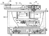
본 발명에 따른 웨이퍼 운반 장치가 제 1 도 및 제 2 도에 도시되어 있다. 간략하면, 장치는 다음과 같이 작동한다. 다수의 웨이퍼(12)를 각각 유지하는 카세트 홀더(10)가 카세트 록(14, 16, 18)에 놓여있다. 카세트 록(14, 16, 18)은 진공 배기되고 카세트 홀더(10)는 진공 엘리베이터 실(20)로 하강된다. 웨이퍼는 웨이퍼 운반 아암(22)에 의해 한번에 한개씩 카세트 홀더(10)로부터 빼내어지고, 아암(22)상의 웨이퍼 위치가 감지되는 위치 및 방향 설정 스테이션(26)으로 가서 운반 진공실(24)로 이동된다. 필요시, 웨이퍼의 각도 방향은 변경될 수 있다. 이때 아암(22)은 x 축을 따라서 신장되고 웨이퍼는 처리 시스템의 입력 스테이션(28)으로 운반된다. 입력 스테이션(28)에 웨이퍼를 놓으면 위치 및 방향 설정 스테이션(26)에서 감지된 위치 에러는 변위를 보상함으로써 소거된다. 입력 스테이션(28)에는 운반 아암(22)으로부터 웨이퍼를 제거하는 승강 핀(30)을 포함하는 수단이 제공된다. 처리후, 운반 아암(22)은 위치 및 방향 설정 스테이션(26)을 사용하지 않고 웨이퍼를 카세트 홀더(10)로 귀환시킨다. 웨이퍼가 외측 카세트 록(14, 18)의 어느 것으로부터 운반될 때, 운반 아암(22)은 각 카세트 록에의 접근을 위해 y-축을 따라 측방 으로 이동된다. 웨이퍼는 카세트로부터 제거되고, 운반 아암은 중심 위치로 되돌아가며 아암은 입력 스테이션(28)으로 연장된다. 본 발명에 따른 웨이퍼 운반 시스템의 구조 및 작동에 대해 이후 상세히 기술한다.A wafer transfer apparatus according to the present invention is shown in FIG. 1 and FIG. 2. Briefly, the device operates as follows. A
각 카세트 록(14, 16, 18)은 카세트 홀더(10)와 저판(34)의 삽입 및 제거를 위해 승강할 수 있는 덮개(32)에 의해 폐쇄된다. 카세트 록(14, 16, 18)은 그 진공화를 위해 진공 펌핑 시스템(도시되지 않음)에 연결된다. 록(14, 16, 18)은 각각 밀봉되고 진공 펌핑 시스템에 연결되어 카세트 홀더(10)는 다른 록이 진공하에 있을 때 한 록내에서 교환 될 수 있다. 저판(34)은 카세트 지지판(36)에 의해 밀봉된 개구(35)를 포함한다. 지지판(36)은 카세트의 교환중 저판(34)에 0링(37)으로 밀봉되고 시스템에 의해 웨이퍼를 운반하도록 카세트 엘리베이터 시스템에 의해 하강된다. 밀봉된 벨로즈(41)는 각 카세트 홀더(10)의 상부와 지지판(36)에 설치된 L 형 브래킷(43)사이에 위치하여 카세트 홀더(10)상을 연장하고 있다. 벨로즈(41)는 록이 개방될 때 대기압에 의해 수축되며 록이 진공 펌핑될 때 다시 팽창하기에 충분한 가스를 포함한다. 팽창 상태에서 벨로즈(41)는 카세트 홀더(10)를 받침목(138)에 대해 하방에 확고히 유지시키고 카세트 홀더(10)의 뒤틀림을 방지한다.Each
지지판(36)의 저면에 연결된 엘리베이터 축(38)은 엘리베이터 실(20)을 지나 직류 서보 모터인 엘리베이터 구동체(40)로 이어져있다. 엘리베이터 실(20)은 카세트 록(14, 16, 18)의 공통벽으로서의 저판(34)과 지지판(36)을 포함하는 하우징(42)에 의해 규정된다. 엘리베이터 실(20)은 그 진공화를 위해 진공 펌핑 시스템(도시되지 않음)에 연결된다. 엘리베이터 축(38)은 벨로즈(44)에 의해 엘리베이터실(20)의 내부로부터 밀봉된다. 엘리베이터 구동체(40)는 엘리베이터 실(20) 외측에 위치하여 카세트 홀더(10)를 상하 이동시키고 또 카세트 홀더의 교환시에 저판(34)에 카세트 지지판(36)을 밀봉시키는 능력을 제공한다. 엘리베이터 실은 운반 아암(22)에 의한 접근을 위해 운반 진공실(24) 안에 개구(48)를 포함한다. 개구(48)에는 보수를 위해 엘리베이터 실(20)의 차단을 위해 밸브(도시되지 않음)를 구비하고 있다.An
본 예에서, 입력 스테이션(28)은 다수의 웨이퍼를 일괄처리형 이온 주입 시스템에 장착하는 디스크(47)이다. 웨이퍼는 본 발명의 웨이퍼 운반 장치에 의해 한번에 하나씩 디스크 주변 근처에 장착된다. 웨이퍼의 로딩 및 언로딩시에, 디스크는 증분적으로 회전하여 디스크상의 각 웨이퍼 장착 위치는 웨이퍼 운반 시스템에 제공된다. 본 발명의 웨이퍼 운반 장치는 어떠한 형태의 처리 시스템에서도 웨이퍼를 입력 스테이션으로 운반할 수 있음을 이해할 것이다.In this example, the
보통은 갯수가 3 개인 승강핀(30)은 디스크(47)상의 웨이퍼 지지 압반(49)의 구멍을 통해 공기 작동식 실린더(50)에 의해 상.하로 이동된다. 핀(30)은 아암(22)에 의한 제거를 위해 압반(49)면으로부터 웨이퍼를 들어올리거나, 또는 압반(49)면상의 배치를 위해 운반 아암(22)으로부터 웨이퍼를 들어올린다. 후술하겠지만, 운반 아암(22)은 웨이퍼와 압반(49)사이를 지나는, 비교적 얇고 평평한 웨이퍼픽을 포함한다. 웨이퍼가 디스크(47)상에 로딩될 때 핀(30)은 이때 후퇴하는 운반 아암(22)으로부터 웨이퍼를 들어올린다. 웨이퍼를 디스크로부터 제거할 때, 웨이퍼는 핀(30)에 의해 들어올려지고, 운반 아암(22)은 웨이퍼와 압반(49)사이로 신장되며, 승강핀(30)은 하강되어, 운반 아암(22)상에 웨이퍼를 내려놓는다. 통상, 웨이퍼는 입력 스테이션(28)에서 압반(49)면에 클램프된다. 다른 방법으로서 웨이퍼는 입력 스테이션으로부터 처리 시스템내의 다른 위치로 이동 될 수 있다.The
운반 진공실(24)은 하우징(51)에 의해 규정되고 그 진공화를 위해 진공 펌핑시스템(도시되지 않음)에 연결된다. 운반 아암(22)은 진공실(24)내에 위치하고 운반 구동 시스템(52)에 의해 지지 및 작동된다. 구동 시스템(52)은 운반 아암(22)을 지지하고 구동하는 구동 조립체(54)를 포함한다. 구동 조립체(54)와 아암(22)은 제1도에 도시된 y-축을 따라 측방으로 이동할 수 있다. 구동 조립체(54)는 진공실(24) 외측에 위치한 구동 모터와 이송 나사(58)의 제어하에서 y-축을 따라 이동할 수 있다. 제 4 도 및 제 5 도에 도시된 바와같이, 구동 조립체(54)는 U 자형 지지 브래킷(60)에 설치된다. 안내 트랙(62)은 카세트 록(14, 16, 18)의 전방에서 y-축에 평행하게 진공실(24)을 가로질러 설치된다. 지지 브래킷(60)은 선형레일(64)에 의해 안내 트랙(62)에 연결된다.The
이송 나사(58)는 지지 브래킷(60)에 부착되어 모터(56)에 의해 작동될 때 선형 레일(64)을 따라 지지 브래킷(60)과 구동 조립체(54)의 조합을 구동시킨다.The
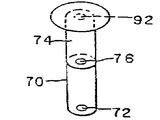
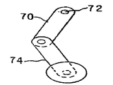
제 3 도에서, 웨이퍼 운반 아암(22)은 제 1 축(72)에 관해 회전하도록 제 1 축(72)에서 구동 조립체(54)에 연결된 신장된 제 1 부분(70)을 포함한다. 신장된 제 2 부분(74)은 피버트 축(76)에 관해 회전하도록 제 1 부분(70)에 연결된다.The
피버트 축(76) 반대편의 제 2 부분(74) 끝 근방에는 웨이퍼 지지 픽(80)이 구비된다. 제 1 풀리(84)는 구동 조립체(54) 상의 고정 위치에서 제 1 축(72)상에 설치된다. 제 2 풀리(86)는 피버트 축(76)상의 제 2 부분(74)에 고정된다. 구동 벨트(88)는 제 1 풀리(84)와 제 2 풀리(86)를 연결한다. 벨트 장력기(90)는 구동 벨트(88)의 인장을 조정하는 수단을 제공 한다. 양호하게는 제 1 풀리(84)는 제 2 풀리(86)의 직경의 2 배이다. 이러한 직경비로서, 제 1 부분(70)이 제 1 축(72)에 관해 회전하면 제 2 부분(74)은 제 1 부분(70)의 각 속도 2 배로 피버트 축(76)에 관해 회전하게 된다. 즉, 제 1 부분(70)의 각각의 회전에 대해 제 2 부분(74)은 2 배의 선회를 하게 된다. 이러한 배치에 의해, 제 1 축(72)과 피버트 축(76)간의 거리가 피버트 축(76)과 공칭 웨이퍼 중심(92)간의 거리와 같을 때, 웨이퍼 픽(80)상의 공칭 웨이퍼 중심(92)의 선형 운동이 제공된다.A wafer support pick 80 is provided near the end of the
제 2 부분(74)의 먼 끝쪽에 있는 웨이퍼 픽(80)은, 카세트 홀더(10)내의 웨이퍼 사이에의 접근을 허용하기 위해 전형적으로 1.27mm(0.050 인치) 또는 그 미만의 박막 평판 금속 시트이다. 공칭 웨이퍼 중심(92)은 이상적으로는 운반중 웨이퍼 중심과 일치된다. 웨이퍼 픽(80)의 상면에는, 웨이퍼에 의한 접촉 부위에서 높은 마찰 계수를 가진 폴리우레탄 또는 다른 재료로된 여러개의 패드(94)가 구비된다. 패드(94)는 웨이퍼와 픽(80)간의 마찰을 높여서 웨이퍼가 픽으로 부터 부주의하게 미끄러지는 것을 방지한다. 또한, 픽(80)에는, 웨이퍼 둘레와 정합하는 초생달 형상으로서 공칭 웨이퍼 위치의 둘레에 위치하는 상승 정지체(96)가 구비된다. 정지체(96)는 웨이퍼가 카세트 홀더(10)로부터 제거될 때 픽(80) 상에 웨이퍼를 적절히 위치시키는 것을 도와준다. 픽(80)상의 웨이퍼의 존재를 감지하기 위해 제 2 부분(74)의 상면, 양호하게는 피버트 축(76)가까이에 압전저항 변형 게이지와 같은 변형 게이지(98)가 설치된다. 본 기술분야에서 주지된 바와같이 변형 게이지(98)는 웨이퍼의 무게에 의해 생기는 제 2 부분(74)에서의 변형에 따른 전기 신호를 제공한다. 감지 능력을 향상시키기 위해 제 2 부분(74)은 그 길이를 통해 얇고 평평한 부재로 된다. 또, 웨이퍼 픽(80)에는, 이후 기술하는 웨이퍼 방향 설정기의 작동을 위해 웨이퍼 중심(92)과 동심인 구멍(100)이 구비된다.The wafer pick 80 at the far end of the
웨이퍼 운반 아암(22)의 운동은 제6a도 내지 제6e도에 도시되어 있다. 연결 수단인 제 1 및 제 2 풀리(84, 86)와 구동 벨트(88)의 배치로 제 2 부분(74)은 제 1 부분(70)의 2 배의 각 속도로 회전된다. 게다가, 제 1 축(72)과 피버트축(76)간의 거리는 피버트 축(76)과 웨이퍼 중심(92)간의 거리와 같다. 이러한 치수로 웨이퍼는 제 6a 도 내지 제 6e 도에 표시된 바와같이 운반 아암(22)에 의해 직선으로 이동된다. 제 6c 도에서 제 1 부분(70)이 제 2 부분(74)과 겹칠때 공칭 웨이퍼 중심(92)과 구멍(100)은 제 1 축(72)과 정렬된다는 점에 유의해야 한다. 이것은 후술하는 바와같이 웨이퍼 방향 설정기의 작동에 중요하다. 제 6e 도에서, 웨이퍼가 입력 스테이션(28)에 도달할 때 아암(22)이 완전히 신장되지 않는다는 점에 유의해야 한다. 이것은, 부가적인 주행이 소정의 위치에 대해 웨이퍼가 바람직하지 못하게 변위되는 것을 보상하는데 도움이 되기 때문에 후술하는 바와같이 웨이퍼 방향 설정기의 작동에 중요하다. 제 6a 도는 카세트 홀더(10)로부터 웨이퍼의 제거를 위해 완전히 신장된 아암(22)을 도시하고 있다. 제 6c 도는 중립, 또는 원래 위치에 있는 아암(22)을 도시하고 있다. 제 6e 도는 입력 스테이션(28)에서 웨이퍼의 배치를 위해 거의 완전히 신장된 아암(22)을 도시하고 있다. 제 6b 도 및 제 6d 도는 운반 아암(22)의 중간 위치를 도시하고 있다. 다른 웨이퍼 운반 아암 구조에 대해서는 본건과 동시에 출원된 계류중인 리챠드 와인버그의 특허출원(발명의 명칭: "웨이퍼 취급 아암")에 기술되어 있다.The movement of the
본원에 도시되고 기술된 웨이퍼 운반 아암(22)은 아암 구동 모터가 1 "g" 보다 훨씬 낮은 웨이퍼의 가속도를 유지하고 저속으로 이동을 시작하도록 되어 있기 때문에 웨이퍼의 신뢰성 있는 운반에 유리하다. 따라서, 웨이퍼를 떨어뜨릴 수 있는 갑작스런 시동과 정지 및 아암의 높은 가속도가 회피된다.The
제 4 도 및 제 5 도에는, 제 1 축(72)에 관해 회전을 하도록 운반 아암(22)이 구비된 운반 아암 구동 조립체(54)의 상세가 도시되어 있다. 운반 아암(22)을 위한 구동 모터와 관련 설비가 밀봉된 구동 하우징(110)내에 위치되고, 그 내부는 대기로 유지된다. 구동 하우징(110)은 가요성 호스(도시되지 않음)를 경유하여 진공실(24)을 통해 외기에 연결되어 그 내부에서의 대기압을 유지한다. 그 결과, 구동 모터와 설비는 유도 냉각에 의해 적절히 냉각되고, 가동부에 의해 발생되는 먼지등의 입자들은 구동 하우징내에 수용된다. 운반 아암(22)용 구동축(111)은 유체 밀봉체를 통과하여 하우징(110) 내부로 가서 구동축(111)상의 풀리(126), 모터(112)상의 풀리(127) 및 상호 연결 벨트(도시 되지 않음)에 의해 아암 구동 모터(112)에 연결된다. 구동 모터(112)는 운반 아암(22)의 정확한 위치 제어용의 직류 서보 모터가 적합하다.4 and 5 show the details of the carrier
웨이퍼와의 마찰을 위한 폴리우레탄 링을 구비한 평탄 상면을 가진 방향 설정기 척(114)은 제 1 축(72)상의 제 1 부분(70)의 상면에 위치한다. 방향 설정기척(114)은, 그와 동심인 구동축(111)을 통과하면서 구동 하우징(110) 내로 가는 제 1 축(72)상의 척의 축(116)에 의해 지지된다. 척의 축(116)은 공기 실린더(118)에 의해 승강 및 하강된다. 운반 아암이 제6c도에 도시된 바와같이 중립 위치에 있을때, 방향 설정기 척(114)은 제 2 부분(74)내의 구멍(100)을 통해 상승되고 웨이퍼 픽(80)상의 웨이퍼를 들어올린다. 또, 척의 축(116)은 풀리(121, 122) 및 구동 벨트(123)에 의해 방향 설정기 모터(120)에 연결된다. 방향 설정기 모터(120)는 직류 서보 모터로 될 수 있다. 상기와 같이 웨이퍼를 들어 올리기 위해 방향 설정기 척(114)이 공기 실린더(118)에 의해 상승될 때, 모터(120)는 여기되어, 후술하는 바와같이 웨이퍼 위치 감지를 위해 방향 설정기 척(114)과 웨이퍼를 회전시킨다.A direction setting device chuck 114 having a flat top surface with a polyurethane ring for friction with the wafer is located on the top surface of the
제 5 도에 도시된 웨이퍼 위치 및 방향 설정 감지기는 광 센서인 광원(132) 및 광 전지(134)용의 지지 브래킷(130)을 포함 한다. 광원(132)은 웨이퍼 에지 근처에 위치하고 웨이퍼 에지를 가로질러 광 전지(134)로 향한다. 광 전지는 제 1 축(72)과 정렬된 길이 치수로 설치되고 웨이퍼와 광원(132)과 면하고 있다. 웨이퍼는 광원(132)으로부터의 빛의 일부가 광 전지(134)에 도달하는 것을 차단한다. 웨이퍼가 제 1 축(72)에 관해 회전할 때, 광 전지 출력이 감시된다. 만일 웨이퍼가 제 1 축(72)상의 중심에 정확히 놓인다면, 광 전지(134)의 출력은 웨이퍼 평면을 제외하고는 일정하게 유지된다. 평면에서의 신호 변동은 웨이퍼 평면의 각도 방향을 결정하고 방향 설정기 척(114)의 회전에 의해 평면을 소요의 각도 방향으로 보정하는데 사용될 수 있다. 웨이퍼가 제 1 축(72)상의 중심에 정확히 위치되지 않는 통상의 경우, 광 전지(134) 출력은 웨이퍼가 회전함에 따라 변동한다.The wafer position and orientation sensor shown in FIG. 5 includes a
제 7 도에 도시된 바와같이, 제 1 축(72)상의 소요의 웨이퍼 중심(xo, yo)에 대한 실제 웨이퍼 중심을 결정하기 위해 출력 신호 변동이 처리된다.As shown in FIG. 7, the output signal variation is processed to determine the actual wafer center for the desired wafer center (x o , y o ) on the
제 1 도에 도시된 바와같이, 웨이퍼 운반 장치의 y-축은 카세트 홀더와 록(14, 16, 18)에의 접근을 위해 이동될 때 제 1 축(72)에 의해 추종되는 경로로 규정된다. x 축은 입력 스테이션(28)의 중심과 카세트 록(16)내에서 웨이퍼 중심이 그리는 선에 의해 규정된다. 제 1 축(72)은 입력 스테이션(28)에 대해 웨이퍼를 진퇴시키고 또 중간 카세트 록(16)에 대해 웨이퍼를 진퇴시킬 때, 상기 규정된 좌표계의 원점에 위치한다.As shown in FIG. 1, the y-axis of the wafer carrier is defined as the path followed by the
본 발명의 방향 설정기에서, 웨이퍼 위치에 대한 보정은 입력 스테이션(28)에 있는 웨이퍼를 보정 위치에 배치함으로써 이루어진다. x 축 에러는 운반 아암(22)의 신장에 대한 보정에 의해 보상된다. 즉, 아암(22)은 x-축 에러를 제거하기 위해 정상 신장보다 많거나 적게 연장된다. y-축 에러는 y-축 에러 양만큼 안내 트랙(62)를 따른 구동 조립체(54)와 전체 운반 아암(22)의 이동에 의해 보상된다. 따라서, 예를들면, 변위 에러가 광 전지(134)와 관련 처리 회로에 의해 xm= -2.54mm(-0.1in)와 ym= -5.08mm(-0.2in)로 결정된다면, 이때 웨이퍼는 다음과 같이 입력 스테이션(28)에 놓인다. x 축 에러는, 정상 위치보다 2.54mm(0.1 in)미만으로 신장된 운반 아암(22)으로 웨이퍼를 입력 스테이션(28)에 배치함으로써 보상된다. 운반 아암(22)과 구동 조립체(54)는 모터(56)와 이송 나사(58)에 의해 원 y 축 에러를 보상하기 위해 5.08mm(0.2in)만큼 그리고 x 방향 보정에 기인하여 새로이 생긴 y 축 에러만큼 플러스 y 방향으로 이동된다. 이때 웨이퍼는, 입력 스테이션(28)에 대해 정확히 중심에 놓인 핀(30)에 의해 입력 스테이션(28)으로 하강된다.In the orientation setter of the present invention, the correction for the wafer position is made by placing the wafer in the
상기한 바와같이, 웨이퍼의 회전 방향 설정은 위치 및 방향 설정 스테이션(26)에서 결정되고 방향 설정기 척(114)의 회전에 의해 보정된다. 운반 아암(22)에 의해 위치 및 방향 설정 스테이션(26)으로부터 입력 스테이션(28)으로 이동될때 웨이퍼는 회전을 받는다는 것을 알 수 있다. 이러한 회전은 방향 설정기 척(114)의 대응 반대 방향 회전에 의해서 계산되고 보상되므로 웨이퍼는 입력 스테이션(28)에서 소요의 방향으로 위치된다.As described above, the rotation direction setting of the wafer is determined at the position and
웨이퍼 회전각의 함수로서 광 전지(134)로부터 나온 신호는 아날로그-디지탈 변환기로 디지탈 형태로 변환되어 3x1 컨볼버와 같은 것에 의해서 데이타가 감소되는 컴퓨터에 공급된다. 다수 및 소수의 평탄부와 노치를 위치시키기 위해, 예정된 임계치 보다 큰 절대값을 가진 컨볼브된 데이타에서의 정점 및 계곡이 확인된다. 컨볼브된 데이타에서 정점으로부터 계곡으로 가로지르는 제로값이 웨이퍼 평면의 각도를 결정한다.The signal from the
기준점 또는 소정 위치에 대해 웨이퍼 중심의 실제 위치를 결정할 때 평면으로부터의 데이타는 삭제되어야 한다.When determining the actual position of the wafer center relative to a reference point or a predetermined position, data from the plane must be erased.
이때 광 전지로부터 저장된 다수의 비처리 데이타점에 대해, 180°벗어난 해당 데이타 점과의 평균차를 산출하여 xi라 한다. 이때 각 xi에 대해 제 1 지점으로부터 90°벗어난 두개의 데이타 지점의 평균차를 산출하여 yi라 한다. 이것은 N 쌍의 (xi, yi)를 발생한다. 좌표계로서 제 1 쌍을 지정하여 좌표계에 대해 다음을 산출한다.At this time, the average difference from the corresponding data points deviating by 180 degrees from the plurality of stored non-processed data points stored from the photo cells is calculated as x i . Here, for each x i , the average difference of two data points out of 90 ° from the first point is calculated to be y i . This generates an N-pair of (x i , y i ). The first pair is specified as the coordinate system and the following is calculated for the coordinate system.

여기서, (xo, yo)는 회전 중심이고, (xm, ym)은 회전 중심에 대한 웨이퍼의 실제 중심이며, ø i 는 좌표계와 (xi, yi)간의 각도이다. 이때,Where (x o , y o ) is the center of rotation, (x m , y m ) is the actual center of the wafer with respect to the center of rotation, and ø i is the angle between the coordinate system and (x i , y i ). At this time,
ø = tan-1(ym/xm) ø = tan -1 (y m / x m)
![]()
![]()
여기서, Φ는 실제 웨이퍼 중심에 대한 각도이고, Re 는 실제 웨이퍼의 거리이다.Here, [phi] is the angle with respect to the actual wafer center, and Re is the actual wafer distance.
다음, 웨이퍼 각도 방향을 고려한다. 입력 스테이션(28)에서 웨이퍼 평면의 소요의 각도를 α로 하자. 아암(22)이 웨이퍼를 위치 및 방향 설정 스테이션(26)으로부터 입력 스테이션(28)으로 운반할 때, 제 1 도에 도시된 바와같이 아암(22)이 입력 스테이션(28)으로 신장되면 아암(22)과 x 축간의 각도와 동일한 각도만큼 웨이퍼가 회전된다. 본 예에서 이 각도는 21.4°이다. 위치 및 방향 설정 스테이션(26)에서 웨이퍼 평면의 중심점을 α -21.4°만큼 회전시킨다. 웨이퍼 중심이 회전 중심으로 부터 변위하기 때문에 웨이퍼 중심은 β=(α -21.4°)-θ(여기서, θ는 웨이퍼 평면의 초기 각도임) 만큼 회전하여 (xd, yd)로 된다.Next, the wafer angle direction is considered. Let the angle of the wafer plane at the

지금, 웨이퍼를 입력 스테이션(28)으로 운반하면(xd, yd)를 (xd', yd')로 회전시킨다.Now, carrying the wafer to the

웨이퍼 평면은 소요의 채널링 각도로부터(21.4° -dθ)여분으로 회전되고, 여기서, dθ=cos-1(L+xd')/(2M), 이때 L 은 전체 선형 변위이고 M 은 제 1 아암의 길이이다. 이때, 우선 위치 및 방향 설정 스테이션(26)에서 웨이퍼 평면의 중심점을 (β-(21.4° -dθ))로 회전시킨다. 이때 입력 스테이션(28)에서 웨이퍼를 완전히 정렬해서 위치시키기 위해 dθ 로 아암(22)을 회전시킨다.The wafer plane is rotated in excess (21.4 ° -dθ) from channeling angle takes, in which, dθ = cos -1 (L + x d ') / (2M), where L is the total linear displacement and M is the first arm . At this time, the center of gravity of the wafer plane is rotated by (- (21.4 DEG -d?)) In the position and
본원에 기술된 웨이퍼 위치 결정 및 방향 설정 시스템은 향상된 처리 제어를 위해 문자 판독기와 같은 웨이퍼 확인 육안 검사 스테이션에 대한 웨이퍼의 존재 여부 확인에 사용된다.The wafer positioning and orientation system described herein is used to verify the presence of a wafer on a wafer identification visual inspection station, such as a character reader, for improved process control.
본 발명의 제어 시스템의 간단한 블럭도가 제8도에 도시되어 있다. 적절한 메모리와 주변 장치를 구비한 컴퓨터(150)는 상술한 바와같이 아날로그-디지탈 변환기(152)를 통해 광 전지(134)로부터 신호를 받아 처리한다. 컴퓨터(150)는 또한 인터페이스(154) 회로를 통해 변형 게이지(98)로부터 신호를 받는다. 아암 구동 모터(112), 방향 설정기 모터(120), 척 상승 공기 실린더(118), 이송 나사 모터(56), 승강핀 공기 실린더(50) 및 엘리베이터 구동체(40)용의 여기 신호는 적절한 인터페이스 회로를 통해 컴푸터에 의해 공급된다. 고 정확도의 위치 결정을 위해 위치 신호를 서보 모터로부터 컴퓨터로 다시 보내는데 엔코더가 사용된다.A simplified block diagram of the control system of the present invention is shown in FIG. The
작동시, 작동기는 다수의 카세트 록(14, 16, 18)내에 웨이퍼를 포함하는 카세트 홀더(10)를 배치한다. 카세트 록(14, 16, 18)의 덮개(32)는 폐쇄되고, 카세트 록은 엘리베이터 실(20)의 압력 수준에 접근하도록 진공 펌핑된다. 엘리베이터 구동체는 여기되어 카세트 지지판(36)과 카세트 홀더(10)를 운반 아암(22)에 대한 예정된 위치로 하강시킨다. 카세트 지지판(36)은 받침목(138)을 구비하고 상기 받침목은 카세트 홀더(10)의 높이를 상승시키며, 카세트 홀더(10)의 단부가 부분적으로 개방되어 있기 때문에 카세트 홀더(10)내의 최하부 웨이퍼와 지지판(36)의 상부면 사이의 공간(136)에 웨이퍼 픽(80)에 의해 접근을 제공한다. 공간(136)은 운반 아암(22)의 평면상의 중앙에 자리잡아 운반 아암(22)이 이 공간(136)으로 신장된다. 다음, 카세트 홀더(10)는 변형 게이지(98)로부터의 신호에 의해 결정됨에 따라 제 1 웨이퍼가 웨이퍼 지지 픽(80)과 접촉할 때까지 엘리베이터 구동체(40)에 의하여 하방 으로 이동된다. 카세트 엘리베이터는 픽(80)상에 안치되는 제 1 웨이퍼로서 정지된다. 카세트 홀더내의 슬롯간의 공지된 간격에 기초하여 카세트 홀더(10)내의 나머지 웨이퍼의 위치를 산출하기 위하여 제 1 웨이퍼와 웨이퍼 지지픽(80)간의 물리적 접촉이 시스템 컴퓨터에 의해 사용된다. 변형 게이지(98)는, 제 1 웨이퍼와 카세트 슬롯의 간격의 실제 위치에다가 카세트 내의 어떤 공차에 기초하여, 카세트 홀더(10)내에 웨이퍼를 위치시키는 능력을 제공한다. 그러나, 시스템 요소의 공차는 웨이퍼 위치에 포함되지 않는다.In operation, the actuator places the
카세트 홀더(10)로부터 제 1 웨이퍼를 구비한 웨이퍼 지지픽(80)은 운반 아암(22)의 작동에 의해 위치 및 방향 설정 스테이션(26)으로 이동된다. 웨이퍼 픽(80)상의 웨이퍼를 상승시키기 위해 방향 설정기 척(114)이 공기 실린더(118)의 작동에 의해 상승된다. 이때 웨이퍼는 방향 설정기 모터(120)의 작동에 의해 적어도 완전한 1 회전을 한다. 회전중 광원(132)과 광 전지(134)는 제 1 축(72)에 대한 웨이퍼 위치를 감지하고 상기한 바와같이 보정치 xm, ym을 결정한다. 게다가, 광전지(134)와 그 관련 회로는 웨이퍼 평면의 방향을 결정 한다. 이때 방향 설정기척(114)은 웨이퍼 평면이 아암(22)에 의한 후속의 회전 보상으로 소요의 방향에 있을 때까지 다시 회전된다. 이때, 아암(22)은 상기한 바와같이 이루어진 필요한 위치 보정치 xm, ym으로 입력 스테이션(28)으로 신장된다.The wafer support pick 80 with the first wafer from the
외측 카세트 록(14, 18)의 어느 것으로부터 웨이퍼를 제거할 때, 운반 아암(22)과 구동 조립체(54)는 모터(56)와 이송 나사(58)에 의해 안내트랙(62)을 따라 각 카세트 록의 전방 위치로 이동된다. 웨이퍼는 상기한 바와같이 카세트 홀더로 부터 빠져나와 위치 및 방향 설정 스테이션(26)으로 이동된다. 이때, 운반 아암(22)과 구동 조립체(54)는 x 축상의 중심 위치로 다시 이동된다. 위치 및 방향 설정 감지가 수행되고, 웨이퍼는 상술한 바와같이 입력 스테이션(28)으로 운반 된다. 웨이퍼가 보정된 위치로 입력 스테이션에 도달할 때, 웨이퍼 지지픽(80)으로 부터 웨이퍼를 상승시키기 위해 공기 실린더(50)에 의해 핀(30)이 상승된다. 운반 아암(22)은 웨이퍼 아래로부터 물러나고, 웨이퍼는 핀(30)에 의해 웨이퍼 지지 압반 또는 입력 스테이션(28)에서의 다른 웨이퍼 지지 수단상에 내려진다. 다수의 웨이퍼가 예를들어 이온 주입기의 회전 디스크상의 연속 스테이션에 로딩될 때까지, 로딩 공정이 반복될 수 있다. 입력 스테이션(28)으로부터 웨이퍼 제거시, 위치 및 방향 설정 과정이 요구되지 않는 것을 제외하고는 상기 공정은 반대로 된다. 웨이퍼는 필요하면 y 축을 따른 적절한 병진 이동으로 직접 입력 스테이션(28)으로 부터 카세트 홀더로 이동된다.The
본 발명의 웨이퍼 운반 장치는, 다수의 웨이퍼가 입력 스테이션(28)에 연속적으로 로딩되고 후에 입력 스테이션(28)으로부터 연속적으로 제거될 수 있도록 프로그램될 수 있다는 것을 이해할 것이다. 필요시, 한 웨이퍼가 입력 스테이션으로 부터 제거되고 디스크가 새 위치로 회전되기 전에 새 웨이퍼가 로딩되도록 로딩과 언로딩 과정이 바뀌어 질 수 있다. 게다가, 시스템은 프로그램 가능한 방식으로 카세트로 부터 웨이퍼를 로딩과 언로딩할 수 있는 능력을 가진다. 즉, 웨이퍼 픽(80)은 예정된 카세트의 예정된 슬롯으로부터 웨이퍼를 제거하고, 슬롯이 비어 있다면 예정된 카세트의 예정된 슬롯내의 웨이퍼를 교체할 수 있다.It will be appreciated that the wafer transport apparatus of the present invention can be programmed such that a plurality of wafers can be continuously loaded into the
웨이퍼 감지용 변형 게이지(98)의 사용은 상술한 바와같이 카세트 홀더(10)내의 웨이퍼 위치 결정과 관련된다. 변형 게이지(98)는 또한 운반 처리중 언제든지 웨이퍼가 부러지거나 웨이퍼 지지픽(80)으로부터 부주의하게 떨어지지 않았는가를 결정하는데 사용될 수 있다. 웨이퍼가 부러지면 통상 일부가 떨어지고, 웨이퍼 픽상의 무게를 감소시켜 변형 게이지(98)에 의해 신호 출력상의 변화를 일으킨다. 따라서, 변형 게이지(98)는 웨이퍼의 존재나 부재를 검출하는데 유용하다. 웨이퍼가 떨어지거나 또는 부러지면, 보정이 취해질 수 있도록 시스템이 조작자에게 경보해주는 것이 필요하다.The use of the strain gauge 98 for wafer detection is related to wafer positioning in the
본 발명의 웨이퍼 운반 장치는, 각 카세트 록에의 접근을 위해 y 축을 따라 운반 아암(22)과 구동 조립체(54)의 병진 운동의 필요로, 선형적으로 정렬된 카세트 록(14, 16, 18)과 관련해서 상술되었다. 다른 실시예에서, 카세트 록과 그 관련 카세트 홀더는 운반 아암(22)의 2 개 혹은 3 개의 측면상에 위치하여 제 1 축(72)을 향해 면하고 있다. 이 실시예에서 운반 아암(22)과 구동 조립체(54)는 각 카세트 록의 접근을 위해서, 선형 병진 운동 보다는 회전을 위해 설치된다.The wafer transport apparatus of the present invention includes cassette locks 14, 16, 18 (shown in Figure 1) that are linearly aligned, requiring the translational movement of the
이 실시예에서, 운반 아암은 신장과 수축을 위해 회전될 수 있다. 게다가, 전체 구동 조립체(54)는 운반 아암(22)이 다른 방향, 예를들어 y 축을 따라 신장될 수 있도록 제 1 축(72)에 관해 회전된다. 게다가, 본 발명의 운반 장치는 반도체 웨이퍼 운반에 특히 유용하지만, 얇은 디스크형 작업물도 시스템에 의해 취급될 수 있다는 것을 이해할 것이다.In this embodiment, the carrying arm can be rotated for extension and contraction. In addition, the
본 명세서에서 기술된 웨이퍼 위치 보정 시스템은 웨이퍼 평면방향 설정이 요구되지 않을때 각도 방향 설정 기능없이 사용될 수 있다는 것을 이해할 것이다. 게다가, 상술된 웨이퍼 운반 장치는 진공내에서 작동된다. 그러나, 시스템의 요구 조건이 대기에서 작동하도록 명령될 때 시스템은 대기에서 작동될 수 있다.It will be appreciated that the wafer position correction system described herein can be used without angular orientation setting when wafer plane orientation is not required. In addition, the above-described wafer transport apparatus is operated in a vacuum. However, when the requirements of the system are commanded to operate in the atmosphere, the system can be operated in the atmosphere.
본 발명의 양호한 실시예를 고려하여 도시되고 설명 되었지만, 첨부된 청구 범위에서 한정된 바와같이 본 발명의 범위로부터 벗어나지 않고서도 여러가지 변경과 수정이 가해 질 수 있음은 본 기술분야의 숙련된 자에게는 명백하다.While there have been shown and described what are at present considered preferred embodiments of the invention, it will be apparent to those skilled in the art that various changes and modifications can be made therein without departing from the scope of the invention as defined in the appended claims .
Claims (5)
Applications Claiming Priority (2)
| Application Number | Priority Date | Filing Date | Title |
|---|---|---|---|
| US85681486A | 1986-04-28 | 1986-04-28 | |
| US856814 | 1986-04-28 |
Publications (2)
| Publication Number | Publication Date |
|---|---|
| KR870010617A KR870010617A (en) | 1987-11-30 |
| KR100309932B1 true KR100309932B1 (en) | 2001-12-15 |
Family
ID=25324567
Family Applications (1)
| Application Number | Title | Priority Date | Filing Date |
|---|---|---|---|
| KR1019870004071A KR100309932B1 (en) | 1986-04-28 | 1987-04-28 | Wafer transport apparatus and method |
Country Status (4)
| Country | Link |
|---|---|
| EP (2) | EP0556865B1 (en) |
| JP (1) | JPS6323332A (en) |
| KR (1) | KR100309932B1 (en) |
| DE (2) | DE3752234T2 (en) |
Cited By (3)
| Publication number | Priority date | Publication date | Assignee | Title |
|---|---|---|---|---|
| KR100753290B1 (en) * | 1999-12-23 | 2007-08-29 | 어플라이드 머티어리얼스, 인코포레이티드 | Apparatus and method for robotic alignment of substrates |
| KR100989930B1 (en) | 2008-06-16 | 2010-10-29 | 김은환 | Device for holding wafer, wafer inspection apparatus using the same, and method thereof |
| CN110867407A (en) * | 2019-11-20 | 2020-03-06 | 西北电子装备技术研究所(中国电子科技集团公司第二研究所) | Method for manufacturing comb-shaped bracket of silicon wafer supporting mechanism in diffusion process basket |
Families Citing this family (18)
| Publication number | Priority date | Publication date | Assignee | Title |
|---|---|---|---|---|
| GB2194500B (en) * | 1986-07-04 | 1991-01-23 | Canon Kk | A wafer handling apparatus |
| US4775281A (en) * | 1986-12-02 | 1988-10-04 | Teradyne, Inc. | Apparatus and method for loading and unloading wafers |
| DE3827343A1 (en) * | 1988-08-12 | 1990-02-15 | Leybold Ag | DEVICE ACCORDING TO THE CAROUSEL PRINCIPLE FOR COATING SUBSTRATES |
| JP2926213B2 (en) * | 1988-02-12 | 1999-07-28 | 東京エレクトロン株式会社 | Substrate processing equipment |
| JPH0210727A (en) * | 1988-06-28 | 1990-01-16 | Naoetsu Denshi Kogyo Kk | Method and apparatus for dividing semiconductor wafer |
| EP0361959B1 (en) * | 1988-09-30 | 1996-09-11 | Canon Kabushiki Kaisha | A substrate conveying apparatus |
| US5277539A (en) * | 1988-09-30 | 1994-01-11 | Canon Kabushiki Kaisha | Substrate conveying apparatus |
| DE4310149C2 (en) * | 1993-03-29 | 1996-05-02 | Jenoptik Jena Gmbh | Device for handling disc-shaped objects in a handling level of a local clean room |
| US5902088A (en) * | 1996-11-18 | 1999-05-11 | Applied Materials, Inc. | Single loadlock chamber with wafer cooling function |
| US6152070A (en) | 1996-11-18 | 2000-11-28 | Applied Materials, Inc. | Tandem process chamber |
| US6491491B1 (en) | 1997-10-30 | 2002-12-10 | Sankyo Seiki Mfg. Co., Ltd. | Articulated robot |
| US6257827B1 (en) * | 1997-12-01 | 2001-07-10 | Brooks Automation Inc. | Apparatus and method for transporting substrates |
| US6719516B2 (en) * | 1998-09-28 | 2004-04-13 | Applied Materials, Inc. | Single wafer load lock with internal wafer transport |
| GB2347784B (en) * | 1999-03-11 | 2004-02-11 | Applied Materials Inc | Scanning wheel for ion implantation process chamber |
| US7720558B2 (en) | 2004-09-04 | 2010-05-18 | Applied Materials, Inc. | Methods and apparatus for mapping carrier contents |
| JP5132904B2 (en) * | 2006-09-05 | 2013-01-30 | 東京エレクトロン株式会社 | Substrate positioning method, substrate position detection method, substrate recovery method, and substrate position deviation correction apparatus |
| JP2011161629A (en) * | 2011-06-03 | 2011-08-25 | Kawasaki Heavy Ind Ltd | Substrate conveying robot |
| JP2012035408A (en) * | 2011-11-09 | 2012-02-23 | Kawasaki Heavy Ind Ltd | Substrate carrier robot |
Citations (4)
| Publication number | Priority date | Publication date | Assignee | Title |
|---|---|---|---|---|
| US4457664A (en) * | 1982-03-22 | 1984-07-03 | Ade Corporation | Wafer alignment station |
| EP0152555A2 (en) * | 1984-02-21 | 1985-08-28 | Plasma-Therm, Inc. | Apparatus for conveying a semiconductor wafer |
| US4553069A (en) * | 1984-01-05 | 1985-11-12 | General Ionex Corporation | Wafer holding apparatus for ion implantation |
| JPS61263123A (en) * | 1985-05-16 | 1986-11-21 | Canon Inc | Wafer supplying apparatus |
Family Cites Families (17)
| Publication number | Priority date | Publication date | Assignee | Title |
|---|---|---|---|---|
| US3401568A (en) * | 1966-08-17 | 1968-09-17 | Leland F. Blatt | Carriage drive mechanism |
| US4208159A (en) * | 1977-07-18 | 1980-06-17 | Tokyo Ohka Kogyo Kabushiki Kaisha | Apparatus for the treatment of a wafer by plasma reaction |
| JPS57145326A (en) * | 1980-12-29 | 1982-09-08 | Censor Patent Versuch | Method and device for forming pattern on wafer by photosensing semiconductor wafer |
| US4433951A (en) * | 1981-02-13 | 1984-02-28 | Lam Research Corporation | Modular loadlock |
| JPS5864043A (en) * | 1981-10-13 | 1983-04-16 | Nippon Telegr & Teleph Corp <Ntt> | Positioning device for disc-shaped plate |
| US4458152A (en) * | 1982-05-10 | 1984-07-03 | Siltec Corporation | Precision specular proximity detector and article handing apparatus employing same |
| DE3219502C2 (en) * | 1982-05-25 | 1990-04-19 | Ernst Leitz Wetzlar Gmbh, 6330 Wetzlar | Device for the automatic transport of disc-shaped objects |
| JPS59124589A (en) * | 1982-12-28 | 1984-07-18 | 株式会社東芝 | Industrial robot |
| JPS59125627A (en) * | 1983-01-07 | 1984-07-20 | Toshiba Corp | Measuring device for coordinate of outer circumference of wafer |
| DE3465405D1 (en) * | 1983-02-14 | 1987-09-17 | Aeronca Electronics Inc | Articulated arm transfer device |
| EP0129731A1 (en) * | 1983-06-15 | 1985-01-02 | The Perkin-Elmer Corporation | Wafer handling system |
| JPS60109242A (en) * | 1983-11-18 | 1985-06-14 | Hitachi Ltd | Method of carrying and positioning semiconductor wafer and device therefor |
| JPS60163742U (en) * | 1983-12-22 | 1985-10-30 | 東京エレクトロン株式会社 | semiconductor wafer prober |
| GB2157078B (en) * | 1984-03-30 | 1987-09-30 | Perkin Elmer Corp | Wafer alignment apparatus |
| JPS6122642A (en) * | 1984-07-10 | 1986-01-31 | Ulvac Corp | Wafer carrier system |
| US4657618A (en) * | 1984-10-22 | 1987-04-14 | Texas Instruments Incorporated | Powered load lock electrode/substrate assembly including robot arm, optimized for plasma process uniformity and rate |
| JPS61226287A (en) * | 1985-03-07 | 1986-10-08 | エプシロン テクノロジー インコーポレーテツド | Device and method for treating workpiece |
-
1987
- 1987-04-28 JP JP62103468A patent/JPS6323332A/en active Granted
- 1987-04-28 EP EP93102766A patent/EP0556865B1/en not_active Expired - Lifetime
- 1987-04-28 DE DE3752234T patent/DE3752234T2/en not_active Expired - Fee Related
- 1987-04-28 DE DE3750558T patent/DE3750558T2/en not_active Expired - Fee Related
- 1987-04-28 EP EP87303748A patent/EP0244202B1/en not_active Expired - Lifetime
- 1987-04-28 KR KR1019870004071A patent/KR100309932B1/en not_active IP Right Cessation
Patent Citations (5)
| Publication number | Priority date | Publication date | Assignee | Title |
|---|---|---|---|---|
| US4457664A (en) * | 1982-03-22 | 1984-07-03 | Ade Corporation | Wafer alignment station |
| US4457664B1 (en) * | 1982-03-22 | 1993-08-24 | Ade Corp | |
| US4553069A (en) * | 1984-01-05 | 1985-11-12 | General Ionex Corporation | Wafer holding apparatus for ion implantation |
| EP0152555A2 (en) * | 1984-02-21 | 1985-08-28 | Plasma-Therm, Inc. | Apparatus for conveying a semiconductor wafer |
| JPS61263123A (en) * | 1985-05-16 | 1986-11-21 | Canon Inc | Wafer supplying apparatus |
Cited By (4)
| Publication number | Priority date | Publication date | Assignee | Title |
|---|---|---|---|---|
| KR100753290B1 (en) * | 1999-12-23 | 2007-08-29 | 어플라이드 머티어리얼스, 인코포레이티드 | Apparatus and method for robotic alignment of substrates |
| KR100989930B1 (en) | 2008-06-16 | 2010-10-29 | 김은환 | Device for holding wafer, wafer inspection apparatus using the same, and method thereof |
| CN110867407A (en) * | 2019-11-20 | 2020-03-06 | 西北电子装备技术研究所(中国电子科技集团公司第二研究所) | Method for manufacturing comb-shaped bracket of silicon wafer supporting mechanism in diffusion process basket |
| CN110867407B (en) * | 2019-11-20 | 2023-04-18 | 西北电子装备技术研究所(中国电子科技集团公司第二研究所) | Method for manufacturing comb-shaped bracket of silicon wafer supporting mechanism in diffusion process basket |
Also Published As
| Publication number | Publication date |
|---|---|
| DE3750558D1 (en) | 1994-10-27 |
| EP0244202A2 (en) | 1987-11-04 |
| JPS6323332A (en) | 1988-01-30 |
| EP0556865B1 (en) | 1998-11-18 |
| DE3750558T2 (en) | 1995-02-02 |
| JPH0458184B2 (en) | 1992-09-16 |
| KR870010617A (en) | 1987-11-30 |
| EP0244202A3 (en) | 1990-09-05 |
| DE3752234T2 (en) | 1999-05-12 |
| EP0244202B1 (en) | 1994-09-21 |
| DE3752234D1 (en) | 1998-12-24 |
| EP0556865A1 (en) | 1993-08-25 |
Similar Documents
| Publication | Publication Date | Title |
|---|---|---|
| KR100309932B1 (en) | Wafer transport apparatus and method | |
| US4836733A (en) | Wafer transfer system | |
| EP0219826B1 (en) | Vacuum processing system | |
| US4643629A (en) | Automatic loader | |
| US4620738A (en) | Vacuum pick for semiconductor wafers | |
| KR20070114117A (en) | Method for positioning a wafer | |
| TW202147495A (en) | Wafer transfer device and wafer transfer method capable of achieving a high transfer throughput | |
| JP2009049200A (en) | Substrate processing apparatus, substrate processing method and storage medium | |
| US20090092470A1 (en) | End effector with sensing capabilities | |
| US6964276B2 (en) | Wafer monitoring system | |
| JP2010062215A (en) | Vacuum treatment method and vacuum carrier | |
| JP3674063B2 (en) | Wafer transfer device | |
| KR102095984B1 (en) | Apparatus and method for treating substrate | |
| JPH06211320A (en) | Wafer carrying-in and out device | |
| US7068003B2 (en) | System to determine proper wafer alignment | |
| JPH06236910A (en) | Inspection device | |
| JP2625112B2 (en) | Method for storing processed wafers under desired vacuum conditions | |
| JPH05238513A (en) | Positioning method for semiconductor wafer storage cassette semiconductor wafer carrier mechanism | |
| JPH0582625A (en) | Wafer carrier | |
| US20230051061A1 (en) | Substrate transfer method and substrate transfer device | |
| JP6756600B2 (en) | Substrate processing equipment and substrate processing method | |
| JPH07169819A (en) | Substrate moving and mounting method | |
| CN113261080A (en) | Substrate processing apparatus, furnace mouth sealing unit and method for manufacturing semiconductor device | |
| JPH04215454A (en) | Attitude controller for wafer cassette | |
| JPH0272650A (en) | Substrate containing apparatus |
Legal Events
| Date | Code | Title | Description |
|---|---|---|---|
| A201 | Request for examination | ||
| E902 | Notification of reason for refusal | ||
| E601 | Decision to refuse application | ||
| J2X1 | Appeal (before the patent court) |
Free format text: APPEAL AGAINST DECISION TO DECLINE REFUSAL |
|
| J2X2 | Appeal (before the supreme court) |
Free format text: APPEAL BEFORE THE SUPREME COURT FOR APPEAL AGAINST DECISION TO DECLINE REFUSAL |
|
| J221 | Remand (intellectual property tribunal) |
Free format text: REMAND (INTELLECTUAL PROPERTY TRIBUNAL) FOR APPEAL AGAINST DECISION TO DECLINE REFUSAL |
|
| J301 | Trial decision |
Free format text: TRIAL DECISION FOR APPEAL AGAINST DECISION TO DECLINE REFUSAL REQUESTED 20000126 Effective date: 20000331 |
|
| S901 | Examination by remand of revocation | ||
| E902 | Notification of reason for refusal | ||
| E902 | Notification of reason for refusal | ||
| GRNO | Decision to grant (after opposition) | ||
| GRNT | Written decision to grant | ||
| FPAY | Annual fee payment |
Payment date: 20050905 Year of fee payment: 5 |
|
| LAPS | Lapse due to unpaid annual fee |