JP7699633B2 - ばね部材を有し半導体構造を劈開するための劈開システム、及びそのような構造を劈開するための方法 - Google Patents
ばね部材を有し半導体構造を劈開するための劈開システム、及びそのような構造を劈開するための方法 Download PDFInfo
- Publication number
- JP7699633B2 JP7699633B2 JP2023156214A JP2023156214A JP7699633B2 JP 7699633 B2 JP7699633 B2 JP 7699633B2 JP 2023156214 A JP2023156214 A JP 2023156214A JP 2023156214 A JP2023156214 A JP 2023156214A JP 7699633 B2 JP7699633 B2 JP 7699633B2
- Authority
- JP
- Japan
- Prior art keywords
- cleaving
- suction
- semiconductor structure
- arm
- spring member
- Prior art date
- Legal status (The legal status is an assumption and is not a legal conclusion. Google has not performed a legal analysis and makes no representation as to the accuracy of the status listed.)
- Active
Links
Images


Classifications
-
- B—PERFORMING OPERATIONS; TRANSPORTING
- B32—LAYERED PRODUCTS
- B32B—LAYERED PRODUCTS, i.e. PRODUCTS BUILT-UP OF STRATA OF FLAT OR NON-FLAT, e.g. CELLULAR OR HONEYCOMB, FORM
- B32B38/00—Ancillary operations in connection with laminating processes
- B32B38/18—Handling of layers or the laminate
- B32B38/1858—Handling of layers or the laminate using vacuum
-
- B—PERFORMING OPERATIONS; TRANSPORTING
- B32—LAYERED PRODUCTS
- B32B—LAYERED PRODUCTS, i.e. PRODUCTS BUILT-UP OF STRATA OF FLAT OR NON-FLAT, e.g. CELLULAR OR HONEYCOMB, FORM
- B32B43/00—Operations specially adapted for layered products and not otherwise provided for, e.g. repairing; Apparatus therefor
- B32B43/006—Delaminating
-
- H—ELECTRICITY
- H01—ELECTRIC ELEMENTS
- H01L—SEMICONDUCTOR DEVICES NOT COVERED BY CLASS H10
- H01L21/00—Processes or apparatus adapted for the manufacture or treatment of semiconductor or solid state devices or of parts thereof
- H01L21/67—Apparatus specially adapted for handling semiconductor or electric solid state devices during manufacture or treatment thereof; Apparatus specially adapted for handling wafers during manufacture or treatment of semiconductor or electric solid state devices or components ; Apparatus not specifically provided for elsewhere
- H01L21/67005—Apparatus not specifically provided for elsewhere
- H01L21/67011—Apparatus for manufacture or treatment
- H01L21/67092—Apparatus for mechanical treatment
-
- H—ELECTRICITY
- H01—ELECTRIC ELEMENTS
- H01L—SEMICONDUCTOR DEVICES NOT COVERED BY CLASS H10
- H01L21/00—Processes or apparatus adapted for the manufacture or treatment of semiconductor or solid state devices or of parts thereof
- H01L21/67—Apparatus specially adapted for handling semiconductor or electric solid state devices during manufacture or treatment thereof; Apparatus specially adapted for handling wafers during manufacture or treatment of semiconductor or electric solid state devices or components ; Apparatus not specifically provided for elsewhere
- H01L21/683—Apparatus specially adapted for handling semiconductor or electric solid state devices during manufacture or treatment thereof; Apparatus specially adapted for handling wafers during manufacture or treatment of semiconductor or electric solid state devices or components ; Apparatus not specifically provided for elsewhere for supporting or gripping
- H01L21/6838—Apparatus specially adapted for handling semiconductor or electric solid state devices during manufacture or treatment thereof; Apparatus specially adapted for handling wafers during manufacture or treatment of semiconductor or electric solid state devices or components ; Apparatus not specifically provided for elsewhere for supporting or gripping with gripping and holding devices using a vacuum; Bernoulli devices
-
- H—ELECTRICITY
- H01—ELECTRIC ELEMENTS
- H01L—SEMICONDUCTOR DEVICES NOT COVERED BY CLASS H10
- H01L21/00—Processes or apparatus adapted for the manufacture or treatment of semiconductor or solid state devices or of parts thereof
- H01L21/70—Manufacture or treatment of devices consisting of a plurality of solid state components formed in or on a common substrate or of parts thereof; Manufacture of integrated circuit devices or of parts thereof
- H01L21/77—Manufacture or treatment of devices consisting of a plurality of solid state components or integrated circuits formed in, or on, a common substrate
- H01L21/78—Manufacture or treatment of devices consisting of a plurality of solid state components or integrated circuits formed in, or on, a common substrate with subsequent division of the substrate into plural individual devices
-
- B—PERFORMING OPERATIONS; TRANSPORTING
- B32—LAYERED PRODUCTS
- B32B—LAYERED PRODUCTS, i.e. PRODUCTS BUILT-UP OF STRATA OF FLAT OR NON-FLAT, e.g. CELLULAR OR HONEYCOMB, FORM
- B32B2457/00—Electrical equipment
- B32B2457/14—Semiconductor wafers
Landscapes
- Engineering & Computer Science (AREA)
- Microelectronics & Electronic Packaging (AREA)
- Condensed Matter Physics & Semiconductors (AREA)
- General Physics & Mathematics (AREA)
- Manufacturing & Machinery (AREA)
- Computer Hardware Design (AREA)
- Physics & Mathematics (AREA)
- Power Engineering (AREA)
- Container, Conveyance, Adherence, Positioning, Of Wafer (AREA)
- Dicing (AREA)
- Perforating, Stamping-Out Or Severing By Means Other Than Cutting (AREA)
- Processing Of Stones Or Stones Resemblance Materials (AREA)
- Mechanical Treatment Of Semiconductor (AREA)
- Semiconductor Lasers (AREA)
Description
この出願は、2019年9月27日に出願された米国仮特許出願第62/906,860号の利益を請求し、該出願は、その全体が参照として本書に編入される。
本開示の分野は、半導体構造を劈開するための劈開システム、特に、半導体構造を2つの部分に分離するために蓄積されたばねエネルギーを使用する劈開システムに関する。また、本開示の分野は、そのような劈開システムを使用することによって半導体構造を劈開するための方法に関する。
例1:ばね力と圧縮
Claims (19)
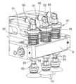
- 上面、及び、上面に平行である底面を有する半導体構造を劈開するための劈開システムであって、
開始位置から、劈開応力が半導体構造に作用される上昇位置まで移動可能な劈開アームと、
半導体構造の上面において半導体構造を把持するための吸引部材と、
劈開アームを通り延在する吸引ロッドと、ここで吸引ロッドは、吸引ロッドの第1端部の方で吸引部材に接続されている、
劈開アームが上昇位置にある状態において、半導体構造に劈開力を作用するばね部材と、
を備えた、劈開システム。 - 吸引ロッドは、ばね部材を通り延在する、請求項1に記載の劈開システム。
- ばね部材は、圧縮ばねである、請求項1に記載の劈開システム。
- ばね部材は、皿ばねである、請求項1に記載の劈開システム。
- ばね部材は、引張ばねであり、ばね部材は、劈開アームの下に配置されている、請求項1に記載の劈開システム。
- 吸引部材は、吸引カップであり、吸引ロッドは、吸引カップに真空を適用するために吸引カップに流体的に接続されその中に形成されたチャネルを含む、請求項1に記載の劈開システム。
- 吸引部材は、第1吸引部材であり、吸引ロッドは、第1吸引ロッドであり、ばね部材は、第1ばね部材であり、当該劈開システムは、
半導体構造を把持する第2吸引部材と、
劈開アームを通り延在する第2吸引ロッドと、ここで第2吸引ロッドは、第2吸引ロッドの第1端部の方で第2吸引部材に接続されている、
劈開アームが上昇位置にある状態において半導体構造に劈開力を作用する第2ばね部材と、
を備える、請求項1に記載の劈開システム。 - 半導体構造を把持する第3吸引部材と、
劈開アームを通り延在する第3吸引ロッドと、ここで第3吸引ロッドは、第3吸引ロッドの第1端部の方で第3吸引部材に接続されている、
劈開アームが上昇位置にある状態において半導体構造に劈開力を作用する第3ばね部材と、
をさらに備えた、請求項7に記載の劈開システム。 - 劈開アームは、劈開アームを開始位置と上昇位置との間で動作させるために旋回軸周りに旋回し、当該劈開システムは、モーターを備え、モーターの作動において劈開アームを旋回させる、請求項1に記載の劈開システム。
- 劈開アームに接続されたベローズ吸引カップをさらに備え、ベローズ吸引カップは、吸引部材に対して半径方向内側に配置されている、請求項9に記載の劈開システム。
- 吸引ロッドは、劈開アームに接続されていない、請求項1に記載の劈開システム。
- 半導体構造の底面において半導体構造を把持するための1つ又は複数の吸引部材を備える、請求項1に記載の劈開システム。
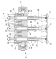
- 上面、及び、上面に平行である底面を有する半導体構造を劈開するための劈開システムであって、
半導体構造の上面において半導体構造を把持するための1つ又は複数の吸引カップと、
吸引ロッドで、該吸引ロッドの第1端部の方で1つ又は複数の吸引カップに接続される吸引ロッドと、
劈開中に半導体構造に劈開力を作用するばね部材と、ここで吸引ロッドは、ばね部材を通り延在する、
を備えた、劈開システム。 - 半導体構造の上面に接触するように構成されたベローズ吸引カップをさらに備え、ベローズ吸引カップは、1つ又は複数の吸引カップに対して半径方向内側に配置されている、請求項13に記載の劈開システム。
- 上面、及び、上面に平行である底面を有する半導体構造を劈開するための方法であって、
半導体構造の上面を吸引カップと接触させること、
半導体構造の上面を把持するために吸引カップに真空を作用させること、
ばね部材に半導体構造において劈開力を作用させるために劈開アームを開始位置から上昇位置へ移動すること、ここでばね部材は、劈開アームが上昇したときにばねエネルギーを蓄積する、
劈開アームが上昇位置にあるときに、半導体構造の劈開を開始するために半導体構造をブレードと接触させること、
半導体構造を劈開面に沿って2つの部分に分離するために半導体構造をブレードと接触させた後、蓄積されたばねエネルギーを解放すること、
を備えた、方法。 - 吸引カップは、劈開アームを通り延在する吸引ロッドに接続され、吸引ロッドは、ばね部材を通り延在する、請求項15に記載の方法。
- 劈開アームが上昇位置に移動するとき、劈開アームは、吸引ロッド軸方向上向きに移動し、
半導体構造が2つの部分に分離されるとき、吸引ロッドは、劈開アームに対して軸方向下向きに移動する、
請求項16に記載の方法。 - ばね部材によって作用される劈開力は、吸引ロッドを介して伝達され、ばね部材によって作用される劈開力は、半導体構造に作用される唯一の劈開力である、請求項16に記載の方法。
- 劈開アームは、劈開の伝播中に移動しない、請求項15に記載の方法。
Applications Claiming Priority (4)
| Application Number | Priority Date | Filing Date | Title |
|---|---|---|---|
| US201962906860P | 2019-09-27 | 2019-09-27 | |
| US62/906,860 | 2019-09-27 | ||
| PCT/US2020/051180 WO2021061480A1 (en) | 2019-09-27 | 2020-09-17 | Cleave systems having spring members for cleaving a semiconductor structure and methods for cleaving such structures |
| JP2022519372A JP7418559B2 (ja) | 2019-09-27 | 2020-09-17 | ばね部材を有し半導体構造を劈開するための劈開システム、及びそのような構造を劈開するための方法 |
Related Parent Applications (1)
| Application Number | Title | Priority Date | Filing Date |
|---|---|---|---|
| JP2022519372A Division JP7418559B2 (ja) | 2019-09-27 | 2020-09-17 | ばね部材を有し半導体構造を劈開するための劈開システム、及びそのような構造を劈開するための方法 |
Publications (2)
| Publication Number | Publication Date |
|---|---|
| JP2023171825A JP2023171825A (ja) | 2023-12-05 |
| JP7699633B2 true JP7699633B2 (ja) | 2025-06-27 |
Family
ID=72709863
Family Applications (2)
| Application Number | Title | Priority Date | Filing Date |
|---|---|---|---|
| JP2022519372A Active JP7418559B2 (ja) | 2019-09-27 | 2020-09-17 | ばね部材を有し半導体構造を劈開するための劈開システム、及びそのような構造を劈開するための方法 |
| JP2023156214A Active JP7699633B2 (ja) | 2019-09-27 | 2023-09-21 | ばね部材を有し半導体構造を劈開するための劈開システム、及びそのような構造を劈開するための方法 |
Family Applications Before (1)
| Application Number | Title | Priority Date | Filing Date |
|---|---|---|---|
| JP2022519372A Active JP7418559B2 (ja) | 2019-09-27 | 2020-09-17 | ばね部材を有し半導体構造を劈開するための劈開システム、及びそのような構造を劈開するための方法 |
Country Status (7)
| Country | Link |
|---|---|
| US (3) | US11538698B2 (ja) |
| EP (1) | EP4035202B1 (ja) |
| JP (2) | JP7418559B2 (ja) |
| KR (2) | KR102710431B1 (ja) |
| CN (1) | CN114556540A (ja) |
| TW (1) | TWI833039B (ja) |
| WO (1) | WO2021061480A1 (ja) |
Families Citing this family (2)
| Publication number | Priority date | Publication date | Assignee | Title |
|---|---|---|---|---|
| JP7309191B2 (ja) * | 2019-11-06 | 2023-07-18 | 中村留精密工業株式会社 | ウェハー分割装置 |
| US12270768B2 (en) * | 2020-09-16 | 2025-04-08 | Globalwafers Co., Ltd. | Method of processing a cleaved semiconductor wafer |
Citations (5)
| Publication number | Priority date | Publication date | Assignee | Title |
|---|---|---|---|---|
| JP2000150456A (ja) | 1998-11-06 | 2000-05-30 | Canon Inc | 試料の分離装置及び分離方法 |
| JP2015076570A (ja) | 2013-10-11 | 2015-04-20 | 東京エレクトロン株式会社 | 剥離装置、剥離システム、剥離方法、プログラム及びコンピュータ記憶媒体 |
| JP2015162569A (ja) | 2014-02-27 | 2015-09-07 | 東京エレクトロン株式会社 | 剥離方法、プログラム、コンピュータ記憶媒体、剥離装置及び剥離システム |
| JP2017168563A (ja) | 2016-03-15 | 2017-09-21 | 日本電気硝子株式会社 | 基板の剥離装置 |
| WO2019044530A1 (ja) | 2017-09-04 | 2019-03-07 | リンテック株式会社 | 薄型化板状部材の製造方法、及び製造装置 |
Family Cites Families (15)
| Publication number | Priority date | Publication date | Assignee | Title |
|---|---|---|---|---|
| JP2726002B2 (ja) * | 1994-06-06 | 1998-03-11 | 株式会社アマダ | 一枚取り装置 |
| US5676364A (en) | 1994-08-19 | 1997-10-14 | Amada Company, Limited | Plate material separating apparatus |
| JPH115064A (ja) * | 1997-06-16 | 1999-01-12 | Canon Inc | 試料の分離装置及びその方法並びに基板の製造方法 |
| US6263941B1 (en) | 1999-08-10 | 2001-07-24 | Silicon Genesis Corporation | Nozzle for cleaving substrates |
| JP4517315B2 (ja) | 1999-10-08 | 2010-08-04 | 株式会社ニコン | 基板落下防止機構およびこれを備えた基板検査装置 |
| JP2004335930A (ja) * | 2003-05-12 | 2004-11-25 | Juki Corp | ウェハの劈開方法及び劈開装置 |
| AU2003235243A1 (en) | 2003-05-13 | 2004-12-03 | Mimasu Semiconductor Industry Co., Ltd. | Wafer demounting method, wafer demounting device, and wafer demounting and transferring machine |
| US20050150597A1 (en) * | 2004-01-09 | 2005-07-14 | Silicon Genesis Corporation | Apparatus and method for controlled cleaving |
| US7427554B2 (en) | 2005-08-12 | 2008-09-23 | Silicon Genesis Corporation | Manufacturing strained silicon substrates using a backing material |
| US8993410B2 (en) | 2006-09-08 | 2015-03-31 | Silicon Genesis Corporation | Substrate cleaving under controlled stress conditions |
| US11389171B2 (en) * | 2006-11-21 | 2022-07-19 | David S. Goldsmith | Integrated system for the infixion and retrieval of implants |
| US8845859B2 (en) | 2011-03-15 | 2014-09-30 | Sunedison Semiconductor Limited (Uen201334164H) | Systems and methods for cleaving a bonded wafer pair |
| CN108140605B (zh) | 2015-10-16 | 2022-06-07 | Agc株式会社 | 层叠体的剥离装置和剥离方法及电子器件的制造方法 |
| JP2018043377A (ja) * | 2016-09-13 | 2018-03-22 | 株式会社Screenホールディングス | 剥離装置および剥離方法 |
| JP6999691B2 (ja) | 2017-04-11 | 2022-01-19 | ミュールバウアー ゲゼルシャフト ミット ベシュレンクテル ハフツング ウント コンパニー コマンディトゲゼルシャフト | 光学センサを有するコンポーネント受け取り装置 |
-
2020
- 2020-09-10 US US17/017,319 patent/US11538698B2/en active Active
- 2020-09-17 KR KR1020227013720A patent/KR102710431B1/ko active Active
- 2020-09-17 KR KR1020237031711A patent/KR20230137484A/ko active Pending
- 2020-09-17 JP JP2022519372A patent/JP7418559B2/ja active Active
- 2020-09-17 EP EP20785642.8A patent/EP4035202B1/en active Active
- 2020-09-17 WO PCT/US2020/051180 patent/WO2021061480A1/en not_active Ceased
- 2020-09-17 CN CN202080072907.2A patent/CN114556540A/zh active Pending
- 2020-09-22 TW TW109132794A patent/TWI833039B/zh active
-
2022
- 2022-09-29 US US17/956,402 patent/US12148635B2/en active Active
-
2023
- 2023-09-21 JP JP2023156214A patent/JP7699633B2/ja active Active
-
2024
- 2024-06-11 US US18/739,890 patent/US12334369B2/en active Active
Patent Citations (5)
| Publication number | Priority date | Publication date | Assignee | Title |
|---|---|---|---|---|
| JP2000150456A (ja) | 1998-11-06 | 2000-05-30 | Canon Inc | 試料の分離装置及び分離方法 |
| JP2015076570A (ja) | 2013-10-11 | 2015-04-20 | 東京エレクトロン株式会社 | 剥離装置、剥離システム、剥離方法、プログラム及びコンピュータ記憶媒体 |
| JP2015162569A (ja) | 2014-02-27 | 2015-09-07 | 東京エレクトロン株式会社 | 剥離方法、プログラム、コンピュータ記憶媒体、剥離装置及び剥離システム |
| JP2017168563A (ja) | 2016-03-15 | 2017-09-21 | 日本電気硝子株式会社 | 基板の剥離装置 |
| WO2019044530A1 (ja) | 2017-09-04 | 2019-03-07 | リンテック株式会社 | 薄型化板状部材の製造方法、及び製造装置 |
Also Published As
| Publication number | Publication date |
|---|---|
| US20210098272A1 (en) | 2021-04-01 |
| US20230031395A1 (en) | 2023-02-02 |
| US12334369B2 (en) | 2025-06-17 |
| CN114556540A (zh) | 2022-05-27 |
| JP2023171825A (ja) | 2023-12-05 |
| US20240332042A1 (en) | 2024-10-03 |
| EP4035202A1 (en) | 2022-08-03 |
| US12148635B2 (en) | 2024-11-19 |
| JP2022550363A (ja) | 2022-12-01 |
| US11538698B2 (en) | 2022-12-27 |
| WO2021061480A1 (en) | 2021-04-01 |
| KR20220071229A (ko) | 2022-05-31 |
| TW202403938A (zh) | 2024-01-16 |
| EP4035202B1 (en) | 2023-08-16 |
| JP7418559B2 (ja) | 2024-01-19 |
| TW202127566A (zh) | 2021-07-16 |
| KR102710431B1 (ko) | 2024-09-25 |
| KR20230137484A (ko) | 2023-10-04 |
| TWI833039B (zh) | 2024-02-21 |
Similar Documents
| Publication | Publication Date | Title |
|---|---|---|
| JP7699633B2 (ja) | ばね部材を有し半導体構造を劈開するための劈開システム、及びそのような構造を劈開するための方法 | |
| US9925755B2 (en) | Clamping apparatus for cleaving a bonded wafer structure and methods for cleaving | |
| KR101265830B1 (ko) | 엣지 그립 장치 및 이를 구비하는 로봇 | |
| US6468879B1 (en) | Method and device for separating a plate of material, in particular semiconductor material, into two wafers | |
| US20230238268A1 (en) | Simultaneous bonding approach for high quality wafer stacking applications | |
| TWI902008B (zh) | 用於切割半導體結構之具有彈簧構件之切割系統及切割該等結構之方法 | |
| Mäkinen et al. | Thick-film SOI wafers: Preparation and properties | |
| US10128146B2 (en) | Semiconductor substrate polishing methods and slurries and methods for manufacturing silicon on insulator structures | |
| KR102817534B1 (ko) | 이온주입 접합웨이퍼 분리 장치 및 이를 이용한 이온주입 접합웨이퍼 분리 방법 | |
| CN213622181U (zh) | 一种下料夹持装置及下料装置 | |
| JPH10156687A (ja) | レンズホルダーおよびレンズ保持方法 | |
| JPWO2021061480A5 (ja) | ||
| JPH0513315A (ja) | ウエハホールド装置 |
Legal Events
| Date | Code | Title | Description |
|---|---|---|---|
| A521 | Request for written amendment filed |
Free format text: JAPANESE INTERMEDIATE CODE: A523 Effective date: 20230921 |
|
| A621 | Written request for application examination |
Free format text: JAPANESE INTERMEDIATE CODE: A621 Effective date: 20230921 |
|
| A977 | Report on retrieval |
Free format text: JAPANESE INTERMEDIATE CODE: A971007 Effective date: 20241010 |
|
| A131 | Notification of reasons for refusal |
Free format text: JAPANESE INTERMEDIATE CODE: A131 Effective date: 20241119 |
|
| A521 | Request for written amendment filed |
Free format text: JAPANESE INTERMEDIATE CODE: A523 Effective date: 20250203 |
|
| TRDD | Decision of grant or rejection written | ||
| A01 | Written decision to grant a patent or to grant a registration (utility model) |
Free format text: JAPANESE INTERMEDIATE CODE: A01 Effective date: 20250520 |
|
| A61 | First payment of annual fees (during grant procedure) |
Free format text: JAPANESE INTERMEDIATE CODE: A61 Effective date: 20250617 |
|
| R150 | Certificate of patent or registration of utility model |
Ref document number: 7699633 Country of ref document: JP Free format text: JAPANESE INTERMEDIATE CODE: R150 |