JP7686817B1 - Isolator - Google Patents
Isolator Download PDFInfo
- Publication number
- JP7686817B1 JP7686817B1 JP2024020877A JP2024020877A JP7686817B1 JP 7686817 B1 JP7686817 B1 JP 7686817B1 JP 2024020877 A JP2024020877 A JP 2024020877A JP 2024020877 A JP2024020877 A JP 2024020877A JP 7686817 B1 JP7686817 B1 JP 7686817B1
- Authority
- JP
- Japan
- Prior art keywords
- coil
- substrate
- semiconductor chip
- flexible printed
- wiring board
- Prior art date
- Legal status (The legal status is an assumption and is not a legal conclusion. Google has not performed a legal analysis and makes no representation as to the accuracy of the status listed.)
- Active
Links
Images


Classifications
-
- H—ELECTRICITY
- H01—ELECTRIC ELEMENTS
- H01F—MAGNETS; INDUCTANCES; TRANSFORMERS; SELECTION OF MATERIALS FOR THEIR MAGNETIC PROPERTIES
- H01F27/00—Details of transformers or inductances, in general
- H01F27/28—Coils; Windings; Conductive connections
- H01F27/2804—Printed windings
-
- H—ELECTRICITY
- H10—SEMICONDUCTOR DEVICES; ELECTRIC SOLID-STATE DEVICES NOT OTHERWISE PROVIDED FOR
- H10D—INORGANIC ELECTRIC SEMICONDUCTOR DEVICES
- H10D1/00—Resistors, capacitors or inductors
- H10D1/20—Inductors
-
- H—ELECTRICITY
- H10—SEMICONDUCTOR DEVICES; ELECTRIC SOLID-STATE DEVICES NOT OTHERWISE PROVIDED FOR
- H10W—GENERIC PACKAGES, INTERCONNECTIONS, CONNECTORS OR OTHER CONSTRUCTIONAL DETAILS OF DEVICES COVERED BY CLASS H10
- H10W44/00—Electrical arrangements for controlling or matching impedance
- H10W44/501—Inductive arrangements
-
- H—ELECTRICITY
- H10—SEMICONDUCTOR DEVICES; ELECTRIC SOLID-STATE DEVICES NOT OTHERWISE PROVIDED FOR
- H10W—GENERIC PACKAGES, INTERCONNECTIONS, CONNECTORS OR OTHER CONSTRUCTIONAL DETAILS OF DEVICES COVERED BY CLASS H10
- H10W70/00—Package substrates; Interposers; Redistribution layers [RDL]
- H10W70/60—Insulating or insulated package substrates; Interposers; Redistribution layers
- H10W70/611—Insulating or insulated package substrates; Interposers; Redistribution layers for connecting multiple chips together
-
- H—ELECTRICITY
- H10—SEMICONDUCTOR DEVICES; ELECTRIC SOLID-STATE DEVICES NOT OTHERWISE PROVIDED FOR
- H10W—GENERIC PACKAGES, INTERCONNECTIONS, CONNECTORS OR OTHER CONSTRUCTIONAL DETAILS OF DEVICES COVERED BY CLASS H10
- H10W90/00—Package configurations
-
- H—ELECTRICITY
- H10—SEMICONDUCTOR DEVICES; ELECTRIC SOLID-STATE DEVICES NOT OTHERWISE PROVIDED FOR
- H10W—GENERIC PACKAGES, INTERCONNECTIONS, CONNECTORS OR OTHER CONSTRUCTIONAL DETAILS OF DEVICES COVERED BY CLASS H10
- H10W90/00—Package configurations
- H10W90/401—Package configurations characterised by multiple insulating or insulated package substrates, interposers or RDLs
-
- H—ELECTRICITY
- H10—SEMICONDUCTOR DEVICES; ELECTRIC SOLID-STATE DEVICES NOT OTHERWISE PROVIDED FOR
- H10W—GENERIC PACKAGES, INTERCONNECTIONS, CONNECTORS OR OTHER CONSTRUCTIONAL DETAILS OF DEVICES COVERED BY CLASS H10
- H10W74/00—Encapsulations, e.g. protective coatings
- H10W74/10—Encapsulations, e.g. protective coatings characterised by their shape or disposition
- H10W74/111—Encapsulations, e.g. protective coatings characterised by their shape or disposition the semiconductor body being completely enclosed
-
- H—ELECTRICITY
- H10—SEMICONDUCTOR DEVICES; ELECTRIC SOLID-STATE DEVICES NOT OTHERWISE PROVIDED FOR
- H10W—GENERIC PACKAGES, INTERCONNECTIONS, CONNECTORS OR OTHER CONSTRUCTIONAL DETAILS OF DEVICES COVERED BY CLASS H10
- H10W90/00—Package configurations
- H10W90/701—Package configurations characterised by the relative positions of pads or connectors relative to package parts
- H10W90/721—Package configurations characterised by the relative positions of pads or connectors relative to package parts of bump connectors
- H10W90/724—Package configurations characterised by the relative positions of pads or connectors relative to package parts of bump connectors between a chip and a stacked insulating package substrate, interposer or RDL
Landscapes
- Engineering & Computer Science (AREA)
- Power Engineering (AREA)
- Coils Or Transformers For Communication (AREA)
- Combinations Of Printed Boards (AREA)
- Networks Using Active Elements (AREA)
- Near-Field Transmission Systems (AREA)
Abstract
【課題】信頼性の向上したアイソレータを提供することである。
【解決手段】実施形態のアイソレータは、リジッド基板である第1リジッド基板と、前記第1リジッド基板に第1方向に積層されたフレキシブルプリント配線板である第1フレキシブルプリント配線板と、を有する基板と、前記第1フレキシブルプリント配線板に設けられた第1コイルと、前記第1フレキシブルプリント配線板に設けられ、前記第1方向において前記第1コイルと離間し対向する第2コイルと、前記基板の上に設けられた第1半導体チップと、前記基板の上に設けられた第2半導体チップと、前記基板の中に設けられ、前記第1半導体チップと前記第1コイルを接続する第1配線と、前記基板の中に設けられ、前記第2半導体チップと前記第2コイルを接続する第2配線と、を有する。
【選択図】 図3
An object of the present invention is to provide an isolator with improved reliability.
[Solution] An isolator of an embodiment includes a substrate having a first rigid substrate which is a rigid substrate, and a first flexible printed wiring board which is a flexible printed wiring board stacked in a first direction on the first rigid substrate, a first coil provided on the first flexible printed wiring board, a second coil provided on the first flexible printed wiring board and facing and spaced apart from the first coil in the first direction, a first semiconductor chip provided on the substrate, a second semiconductor chip provided on the substrate, a first wiring provided in the substrate and connecting the first semiconductor chip and the first coil, and a second wiring provided in the substrate and connecting the second semiconductor chip and the second coil.
[Selected figure] Figure 3
Description
本発明の実施形態は、アイソレータに関する。 An embodiment of the present invention relates to an isolator.
互いに電気的に絶縁された送信回路と受信回路の間で信号を伝達するためのアイソレータが知られている。アイソレータには、発光素子や受光素子を用いるもののほかに、コイルを用いるものがある。 Isolators are known for transmitting signals between a transmitting circuit and a receiving circuit that are electrically isolated from each other. In addition to isolators that use light-emitting elements and light-receiving elements, there are also isolators that use coils.
本発明が解決しようとする課題は、信頼性の向上したアイソレータを提供することである。 The problem that this invention aims to solve is to provide an isolator with improved reliability.
実施形態のアイソレータは、リジッド基板である第1リジッド基板と、前記第1リジッド基板に第1方向に積層されたフレキシブルプリント配線板である第1フレキシブルプリント配線板と、を有する基板と、前記第1フレキシブルプリント配線板に設けられた第1コイルと、前記第1フレキシブルプリント配線板に設けられ、前記第1方向において前記第1コイルと離間し対向する第2コイルと、前記基板の上に設けられた第1半導体チップと、前記基板の上に設けられた第2半導体チップと、前記基板の中に設けられ、前記第1半導体チップと前記第1コイルを接続する第1配線と、前記基板の中に設けられ、前記第2半導体チップと前記第2コイルを接続する第2配線と、を有する。 The isolator of the embodiment includes a substrate having a first rigid substrate, which is a rigid substrate, and a first flexible printed wiring board, which is a flexible printed wiring board stacked in a first direction on the first rigid substrate, a first coil provided on the first flexible printed wiring board, a second coil provided on the first flexible printed wiring board and facing and spaced apart from the first coil in the first direction, a first semiconductor chip provided on the substrate, a second semiconductor chip provided on the substrate, a first wiring provided in the substrate and connecting the first semiconductor chip and the first coil, and a second wiring provided in the substrate and connecting the second semiconductor chip and the second coil.
別の実施形態のアイソレータは、第1ダイパッドと、前記第1ダイパッドの上に設けられた第1半導体チップと、前記第1ダイパッドと離間して設けられた第2ダイパッドと、前記第2ダイパッドの上に設けられ、リジッド基板である第1リジッド基板と、前記第1リジッド基板に第1方向に積層されたフレキシブルプリント配線板である第1フレキシブルプリント配線板と、を有する基板と、前記第1フレキシブルプリント配線板に設けられた第1コイルと、前記第1フレキシブルプリント配線板に設けられ、前記第1方向において前記第1コイルと離間し対向する第2コイルと、前記基板の上に設けられ、前記基板の中に設けられた第3配線によって前記第2コイルと接続された電極パッドと、前記第1ダイパッド及び前記第2ダイパッドと離間して設けられた第3ダイパッドと、前記第3ダイパッドの上に設けられた第2半導体チップと、前記第1半導体チップと、前記第2ダイパッドとを接続する第1ワイヤと、前記電極パッドと、前記第2半導体チップとを接続する第2ワイヤと、を有する。 An isolator according to another embodiment includes a substrate having a first die pad, a first semiconductor chip provided on the first die pad, a second die pad provided at a distance from the first die pad, a first rigid substrate provided on the second die pad, and a first flexible printed wiring board, which is a flexible printed wiring board stacked on the first rigid substrate in a first direction, a first coil provided on the first flexible printed wiring board, a second coil provided on the first flexible printed wiring board and facing the first coil at a distance in the first direction, an electrode pad provided on the substrate and connected to the second coil by a third wiring provided in the substrate, a third die pad provided at a distance from the first die pad and the second die pad, a second semiconductor chip provided on the third die pad, a first wire connecting the first semiconductor chip and the second die pad, and a second wire connecting the electrode pad and the second semiconductor chip.
以下に、本発明の各実施の形態について図面を参照しつつ説明する。 Each embodiment of the present invention will be described below with reference to the drawings.
なお、図面は模式的または概念的なものであり、各部分の厚みと幅との関係、部分間の大きさの比率などは、必ずしも現実のものと同一とは限らない。また、同じ部分を表す場合であっても、図面により互いの寸法や比率が異なって表される場合もある。 The drawings are schematic or conceptual, and the relationship between the thickness and width of each part, the size ratio between parts, etc. are not necessarily the same as in reality. Even when showing the same part, the dimensions and ratios may be shown differently depending on the drawing.
例えば、本願明細書中に示される断面図において、積層構造が示されるものがあるが、積層構造の各層の厚みの比率は現実のものと同一とは限らない。断面図中では一方の層が他方の層より厚く図示されているような場合であっても、現実では一方の層と他方の層の厚みは同程度である場合や、一方の層が他方の層よりも薄い場合などがあり得る。つまり、本願明細書中の図面に示される厚みなどの寸法は現実のものとは異なる場合がある。 For example, some cross-sectional views shown in this specification show a layered structure, but the thickness ratio of each layer in the layered structure is not necessarily the same as in reality. Even if one layer is shown thicker than the other layer in the cross-sectional view, in reality the thicknesses of the one layer and the other layer may be about the same, or one layer may be thinner than the other layer. In other words, the dimensions such as thicknesses shown in the drawings in this specification may differ from the actual dimensions.
第1リジッド基板から第1フレキシブルプリント配線板へ向かう方向をZ方向(第1方向)とする。また、Z方向と直交する方向をX方向(第2方向)、X方向及びZ方向と交差する方向をY方向(第3方向)とする。なお、X方向、Y方向及びZ方向は本実施形態では直交関係で示しているが、直交に限定されずたがいに交差する関係であればよい。 The direction from the first rigid substrate to the first flexible printed circuit board is the Z direction (first direction). The direction perpendicular to the Z direction is the X direction (second direction), and the direction intersecting the X and Z directions is the Y direction (third direction). Note that the X direction, Y direction, and Z direction are shown in an orthogonal relationship in this embodiment, but are not limited to being orthogonal as long as they intersect with each other.
また、説明のために、Z方向の正の方向を「上」と呼び、Z方向の負の方向を「下」と呼ぶ。ただし、「上」、「下」の方向は、重力方向または半導体装置の実装時における方向に限定されない。 For the sake of explanation, the positive direction in the Z direction will be referred to as "up" and the negative direction in the Z direction will be referred to as "down." However, the "up" and "down" directions are not limited to the direction of gravity or the directions when the semiconductor device is mounted.
なお、本願明細書と各図において、既出の図に関して前述したものと同様の要素には同一の符号を付して詳細な説明は適宜省略する。 In addition, in this specification and each figure, elements similar to those described above with respect to the previous figures are given the same reference numerals and detailed explanations are omitted as appropriate.
(第1実施形態)
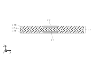
図1は、本実施形態に係るアイソレータ100を例示する模式的平面図である。
First Embodiment
FIG. 1 is a schematic plan view illustrating an
アイソレータ100は、基板10と、第1半導体チップ31と、第1配線41と、第1コイル21と、第2コイル22と、第2配線42と、第2半導体チップ32と、を有する。これらの部材は、図1には図示しない樹脂部70によって覆われている。アイソレータ100は、例えば半導体パッケージである。
The
図1には、第1半導体チップ31及び第2半導体チップ32と接続される外部接続端子は図示されない。アイソレータ100は、例えば後に図3に示すように、リードフレーム61、62を端子として有する。
FIG. 1 does not show external connection terminals connected to the
第1コイル21と第2コイル22を含む複数のコイルは、基板10の中に設けられる。複数のコイルのそれぞれは、平面視において例えば渦巻き状である。第2コイル22は、第1コイル21の上方(Z方向の正の方向)に配置され、第1コイル21から離間している。図1においては、第1コイル21と第2コイル22が重なっている。第1コイル21と第2コイル22とは、磁気的に結合するように設けられる。
A number of coils including a
図1に示す例では、第1コイル21と第2コイル22は、それぞれ2つずつ設けられる。しかしながら、第1コイル21及び第2コイル22の数については、図1に示す例に限定されず、1つずつであってもよいし、3つずつ以上であってもよい。
In the example shown in FIG. 1, two
第1配線41は、第1半導体チップ31と第1コイル21とを電気的に接続する。第2配線42は、第2半導体チップ32と第2コイル22とを電気的に接続する。
The
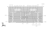
図2は、本実施形態に係るアイソレータ100を例示する模式的平面図である。なお、図1とは異なり、第1コイル21及び第2コイル22の重なる様子を示すために、一部で立体的に表示している。
Figure 2 is a schematic plan view illustrating an
第1半導体チップ31と第1コイル21との間には、第1配線41が設けられる。第1配線41は、例えば複数形成され、それぞれ第1コイル21の中心部及び外縁部に電気的に接続される。ここで、コイルの中心部及び外縁部について、例えば導線を渦巻き状に成型して得られるコイルの一方の端を含む部分を中心部、他方の端を含む部分を外縁部と定義する。第1配線41を介して第1半導体チップ31から第1コイル21へと電気信号を伝達することができる。電気信号とは、例えば電流の向きや大きさ、又は電流の大きさの時間変化を指す。
A
図2は、アイソレータ100が第1コイル21及び第2コイル22をそれぞれ2つずつ有する例を示している。第2コイル22は、それぞれ第1コイル21の上方に配置される。第2コイル22と第2半導体チップ32は、第2配線42によって電気的に接続される。第2配線42は、例えば複数形成され、それぞれ第2コイル22の中心部及び外縁部と電気的に接続される。
Figure 2 shows an example in which the
第1コイル21と第2コイル22が磁気的に結合されるとは、第1コイル21に流れる電流により発生した磁界が第2コイル22を貫き、電磁誘導により第2コイル22を電流が流れることをいう。図2には上向きの矢印により第1コイル21によって発生するZ方向の正の方向の磁界を図示している。第2コイル22が第1コイル21の上方に設けられているため、図示した磁界は、第2コイル22を貫く。
The
次に図2を参照しつつ、アイソレータ100の動作について説明する。以下では第1半導体チップ31は入力側であり、第2半導体チップ32は出力側である例について述べる。アイソレータ100は、たがいに絶縁されている第1半導体チップ31から第2半導体チップ32へと、信号を伝達する。
Next, the operation of the
まず、第1半導体チップ31に入力信号が流れると、入力信号は第1配線41を介して、第1コイル21へと流れる。第1コイル21を流れる電流は、図2に示すようにZ方向の磁界を生成する。
First, when an input signal flows to the
第2コイル22は第1コイル21から離間しており、第1コイル21と第2コイル22の間には図2には図示しない絶縁体が介在している。つまり、第1コイル21の電位と第2コイル22の電位は一般的には異なるものとすることができる。一方、磁界は絶縁体を通過して第1コイル21から第2コイル22へと到達することが可能である。第2コイル22をZ方向の磁場が貫通することで、第2コイル22に誘導電流が流れる。
The
第2コイル22に流れる電流は、第2配線42を通って第2半導体チップ32へと達する。こうして、第1半導体チップ31から第2半導体チップ32へと、電気信号が伝達される。
The current flowing through the
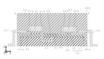
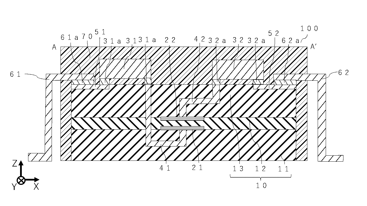
図3は、アイソレータ100の断面構造の一例を示す断面図である。図3は、図1のA-A′線にそった断面図である。
Figure 3 is a cross-sectional view showing an example of the cross-sectional structure of the
図3に示すように、アイソレータ100は、基板10、第1コイル21、第2コイル22、第1半導体チップ31、第2半導体チップ32、第1配線41、第2配線42、導電層51及び52、リードフレーム61及び62、並びに樹脂部70を有する。リードフレーム61及び62の一部は樹脂部70から突出し、アイソレータ100の外部接続端子として用いられる。
As shown in FIG. 3, the
基板10は、第1リジッド基板11、第1フレキシブルプリント配線板12、第2リジッド基板13が積層された構造を有する。第1フレキシブルプリント配線板12は、第1リジッド基板11の上に設けられる。第2リジッド基板13は、第1フレキシブルプリント配線板12の上に設けられる。しかしながら、単に積層されるといった時には、下から上の方向に所定の順序で並んでいるとは限らず、Z方向において重なっていればよい。
The
第1リジッド基板11及び第2リジッド基板13は、例えばエポキシ樹脂を含むリジッド基板である。第1フレキシブルプリント配線板12は、例えばポリイミドや液晶ポリマーを含むフィルムを有するフレキシブルプリント配線板(Frexible Printed Circuit、以下ではFPC基板とも呼ぶ)である。第1フレキシブルプリント配線板12は、例えばポリイミドフィルムやPETフィルムを基材としてフィルム状に形成され、第1リジッド基板11及び第2リジッド基板13よりも剛性の小さい配線板である。
The first
第1フレキシブルプリント配線板12は、第1リジッド基板11と第2リジッド基板13の間に設けられる。第1フレキシブルプリント配線板12の上下方向(Z方向)の両面に導電材料を含む層を配し、コイルを形成することができる。図3に示すように第1フレキシブルプリント配線板12の下面側に第1コイル21を形成し、第1フレキシブルプリント配線板12の上面側に第2コイル22が形成される。
The first flexible printed
第1コイル21と第2コイル22は、基板10の厚さ方向であるZ方向において離間し対向するように設けられる。第1フレキシブルプリント配線板12の詳細な内部構造については、後で図4を参照して述べる。
The
第1半導体チップ31と第1配線41との電気的接続、及び、第1半導体チップ31と導電層51との電気的接続は、接着層31aにより保たれる。図3は、第1半導体チップ31及び第2半導体チップが、下面に複数の電極を有する例を図示している。複数の接着層31aや32aはそれぞれ異なる電極に接続される。
The electrical connection between the
導電層51は、接着層61aによってリードフレーム61に電気的に接続される。接着層31a及び61aは、例えば、はんだや銀ペーストを含む。 The conductive layer 51 is electrically connected to the lead frame 61 by the adhesive layer 61a. The adhesive layers 31a and 61a include, for example, solder or silver paste.
接着層32aは、第2半導体チップ32と第2配線42との電気的接続、及び、第2半導体チップ32と導電層52との電気的接続を保つ。また、導電層52は、接着層62aによってリードフレーム62に電気的に接続される。接着層32a及び62aは、例えば、はんだや銀ペーストを含む。
The adhesive layer 32a maintains the electrical connection between the
なお、図3に示す断面図には図示されないが、第1配線41及び第2配線42は、例えばそれぞれ複数設けられ、第1コイル21及び第2コイル22の中心部及び外縁部と電気的に接続される。
Although not shown in the cross-sectional view of FIG. 3, the
図3に示した例では、第1半導体チップ31及び第2半導体チップ32は下面(Z方向の負の方向の面)において電気信号の入力及び出力を行っている。リードフレーム61から第1半導体チップ31を介して第1配線41へと向かう方向、もしくはその逆の方向に電気信号が伝達される。例えば、第1半導体チップ31は、リードフレームから入力された電気信号を処理して、第1コイル21の中心部及び外縁部のそれぞれに対応した電気信号を生成し、複数の第1配線41へと出力する。また、第2半導体チップ32は、第2コイル22の中心部と外縁部のそれぞれから第2配線42を介して電気信号を受け取り、電気信号を処理してリードフレーム62へと出力をする。
In the example shown in FIG. 3, the
第1半導体チップ31と第1コイル21は、基板10に設けられる第1配線41によって電気的に接続される。第1配線41は、第2リジッド基板13の上面から第2リジッド基板13,第1フレキシブルプリント配線板12の中を伸びて、第1フレキシブル配線板12の下面を通って第1リジッド基板11に達する。第1配線41は、第2リジッド基板13の上面から第1フレキシブル配線板12の下面までの間で、例えばZ方向に沿って設けられてもよい。そして、第1リジッド基板11においてXY平面内で延伸して第1コイル21の下方に到達する。最後にZ方向に伸びて第1コイル21へと接続される。
The
以上、第1配線41の形状の一例を述べたが、第1配線41の形状はこれに限定されない。第1配線41は、Z方向に沿った方向に伸びる部分の割合が大きいほど、第1コイル21が生成する磁界と、第1配線41の周りに発生する磁界と、の干渉による特性の悪化を抑制することができるため望ましい。
Although one example of the shape of the
第2コイル22と第2半導体チップ32は、第2配線42により電気的に接続される。第2配線42は、第2コイル22から、第2リジッド基板13の上面からZ方向の正の方向に第2リジッド基板13の中を伸びる。次に第2リジッド基板13の内部においてXY平面内で延伸する。最後に第2リジッド基板13の中をZ方向に伸びて第2リジッド基板13の上面に達する。以上、第2配線42の形状について述べたが、第2配線42の形状はこれに限定されない。第2配線42は、Z方向に沿った方向に伸びる部分の割合が大きいほど、第2コイル22を貫く磁界と、第2配線42の周りに発生する磁界と、の干渉による特性の悪化を抑制することができるため望ましい。
The
第1配線41及び第2配線42のうち、Z方向に沿う方向に設けられる部分は、例えば基板10をZ方向に掘削してビアホールを形成し、導電材料を埋め込むことで形成することができる。また、第1配線41及び第2配線42のうち、XY平面内に設けられる部分は、リジッド基板である第1リジッド基板11や第2リジッド基板13を多層構造として、導電材料を含む層を形成して得ることができる。
The portions of the
図3を参照しつつ、改めてアイソレータ100の動作について説明する。リードフレーム61は入力端子であり、リードフレーム62は出力端子である場合について述べる。リードフレーム61は導電層51を介して電気信号を第1半導体チップ31に入力する。第1半導体チップ31は、受け取った入力信号に所定の処理を施し、第1配線41へと信号を伝達する。なお、図3の断面構造には表されないが、第1配線41は、第1コイル21の中心部に接続される部分と、外縁部に接続される部分を有していると了解される。
The operation of the
第1コイル21は、第1半導体チップ31からの信号を受け取る。第1コイル21にリードフレーム61が受け取った入力信号に基づいた電流が流れる。第1コイル21に流れる電流は、図3においてZ方向に磁界を生成する。
The
第1フレキシブルプリント配線板12により第1コイル21と電気的に絶縁された第2コイル22に磁界が到達すると、電磁誘導により第2コイル22に電流が流れる。第2コイル22に流れた電流は、電気信号として第2配線42を通って、第2半導体チップ32に至る。第2半導体チップ32は、受け取った電気信号に所定の処理を施して、導電層52を介してリードフレーム62へと出力する。
When the magnetic field reaches the
以下では、本実施形態に係るアイソレータ100の製造方法の一例を説明する。まず、基板10に第1コイル21、第2コイル22、第1配線41、第2配線42、導電層51及び52を形成する。次に接着層31a及び32aを介して第1半導体チップ31及び第2半導体チップ32を載置する。また、接着層61a及び62aを介してリードフレーム61及び62を設ける。そして、リードフレーム61、62のうちで入力及び出力の端子となる部分を除いて樹脂部70により封止する。
Below, an example of a method for manufacturing the
次に図4を参照しつつ、第1フレキシブルプリント配線板12の構造の一例について説明する。第1フレキシブルプリント配線板12は、基材12a及び絶縁体12bを有する。基材12aは、例えばポリイミド又は液晶ポリマーを含むフィルム状の絶縁材料である。絶縁体12bは、例えばプリプレグ等の熱硬化性樹脂を含む。
Next, an example of the structure of the first flexible printed
第1コイル21は基材12aの下面に設けられる。第2コイル22は基材12aの上面に設けられる。第1コイル21及び第2コイル22を覆うように基材12aの上下両面に絶縁体12bが設けられる。ここで、絶縁体12bは、少なくとも第1コイル21や第2コイル22のZ方向の厚みと同等以上の厚みで設けられる。絶縁体12bによって第1フレキシブルプリント配線板12の上下の面を平坦に保つことができる。
The
基板10は、図4に示した第1フレキシブルプリント配線板12の上下に、リジッド基板である第1リジッド基板11及び第2リジッド基板13を設けることで形成される。
The
本実施形態に係るアイソレータ100によれば、基板10にリードフレーム61、62や第1半導体チップ31、第2半導体チップ32を実装する際に第1フレキシブルプリント配線板12の変形を抑制することで、基板10の変形を抑制し、アイソレータの信頼性を向上することが可能である。基板の変形といった時には、基板の屈曲や基板の位置ずれを含むものとする。
According to the
例えば、第1半導体チップ31を載置するときに、基板10は図3において局所的にZ方向の力を受ける。なぜなら、基板10からみてZ方向の正の方向に位置する第1半導体チップ31を、Z方向の負の方向に押すことで基板10に接着する必要があるからである。つまり、第1半導体チップ31を実装することで、基板10には応力がかかる。
For example, when placing the
ここで、比較のために、フレキシブルプリント配線板のみからなる基板に半導体チップを実装する場合について述べる。フレキシブルプリント配線板のみからなる基板では、半導体チップ等の実装時にフレキシブルプリント配線板にかかる応力により、フレキシブルプリント配線板が屈曲する恐れがある。さらには、フレキシブルプリント配線板のみからなる基板はリジッド基板を含む基板よりも軽量であり位置ずれがおこりやすい。つまり、フレキシブルプリント配線板のみからなる基板の場合には、意図しない基板の屈曲及び搭載位置ずれの恐れがある。 For comparison, we will now discuss the case where a semiconductor chip is mounted on a substrate consisting only of a flexible printed wiring board. In a substrate consisting only of a flexible printed wiring board, there is a risk that the flexible printed wiring board will bend due to the stress applied to the flexible printed wiring board when semiconductor chips and the like are mounted. Furthermore, a substrate consisting only of a flexible printed wiring board is lighter than a substrate including a rigid substrate, and is more susceptible to misalignment. In other words, in the case of a substrate consisting only of a flexible printed wiring board, there is a risk of unintended bending of the substrate and misalignment of the mounting position.
一方、本実施形態によれば、基板10はリジッド基板とフレキシブルプリント配線板を含んだ積層構造を有しており、フレキシブルプリント配線板の変形は、重ねられたリジッド基板の剛性がフレキシブルプリント配線板よりも大きいために抑制される。したがって、基板10の変形が抑制され、信頼性を向上することができる。
On the other hand, according to this embodiment, the
基板10は、リジッド基板である第1リジッド基板11及び第2リジッド基板13を有する。例えばFPC基板である第1フレキシブルプリント配線板12は、Z方向においてリジッド基板に挟まれる。したがって、基板10の変形には、2層のリジッド基板を変形させるためのより大きな応力が必要となる。基板10の変形をさらに抑制することができる。
The
第1フレキシブルプリント配線板12の変形を抑制し、実装安定性が向上して基板10の変形に起因する故障および不良を抑制することで、歩留まりを向上することができる。ここで、実装安定性が高いとは、例えば基板10の上に半導体チップやリードフレームを搭載するときに、基板10が変形せずに安定した構造を保つことができることを指す。本実施形態によれば、基板10の変形を抑制することで、アイソレータ100の信頼性を向上することができる。
By suppressing deformation of the first flexible printed
基板10の変形を抑制することで電気的な接続を確実にし、かつ、基板10の変形を抑制することでコイル同士の磁気的結合の効率を良好に保つことができる。したがって、信号伝達にかかる損失を抑制して、信号伝達の性能を向上することができる。
By suppressing deformation of the
また、本実施形態に係るアイソレータ100によれば、第1配線41及び第2配線42は基板10の内部配線によって実現されており、ワイヤ等による電気的接続の必要がない。言い換えると、ワイヤレスの配線が可能である。したがって、ワイヤボンディングの工程を省略することが可能であり、製造効率を向上し、製造工程を短縮することができる。
In addition, according to the
さらに、本実施形態に係るアイソレータ100によれば、フレキシブルプリント配線板である第1フレキシブルプリント配線板12に第1コイル21及び第2コイル22を実装することで、第1コイル21と第2コイル22のZ方向の距離を微細に制御して磁気結合定数を高めることが可能である。第1コイル21と第2コイル22のZ方向の距離が短いほど、第1コイル21が生成する磁界について、損失を少なくして第2コイル22に到達させることができる。つまり、磁気結合定数が大きいとは、第1コイル21から第2コイル22への磁界としての信号の伝達に損失が小さいことをいう。リジッド基板のみからなる基板にコイルを形成する場合と比較して、より厚さの薄いフレキシブルプリント配線板12の上下の面にコイルを形成することで、磁気結合定数を高めることが可能である。
Furthermore, according to the
第1配線41及び第2配線42は、Z方向に沿う部分と、XY平面内に設けられる部分とを含む。第1配線41のうち、第1半導体チップ31の下から第1リジッド基板11へと至る部分に注目すると、配線がZ方向に沿っているため、電流が流れる際に生成される磁界はZ方向に直交する方向である。第1コイル21が生成するZ方向に沿った方向の磁界と、第1配線41のZ方向に沿う部分に電流が流れることで生成する磁界と、は直交する。磁界が直交することで、磁界の干渉を抑制し、ノイズによる信号伝達にかかる特性の悪化を抑制することができる。
The
また、第1配線41や第2配線42のうち、第1リジッド基板11及び第2リジッド基板13内にXY平面に平行に設けられる部分については、第1コイル21及び第2コイル22とZ方向に離間している。第1コイル21及び第2コイル22と離間しているため、磁界の干渉を抑えることができる。
Furthermore, the portions of the
コイル(第1コイル21及び第2コイル22)と、配線(第1配線41及び第2配線42)の間の磁界の干渉は配線のレイアウト等によるため、基板10の変形に伴ってコイルと配線の間の位置関係が変わると、磁界の干渉が助長される恐れがある。本実施形態によれば、基板10の変形を抑制することでコイルと配線の間の磁界の干渉による特性の悪化を抑制することが可能である。
The magnetic field interference between the coils (
(第1実施形態の第1変形例)
図5は、第1実施形態の第1変形例に係るアイソレータ101の断面構造を示している。第1実施形態に係るアイソレータ100と共通する部分については一部説明を省略する。
(First Modification of the First Embodiment)
5 shows a cross-sectional structure of an
本実施形態に係るアイソレータ101は、第1半導体チップ31と第1コイル21、又は、第2半導体チップ32と第2コイル22、を接続する構造が第1実施形態に係るアイソレータ100とは異なる。
The
第1配線41は、第1フレキシブルプリント配線板12に形成された第1部分41aを有する。第1配線41の第1部分41aは、第1フレキシブルプリント配線板12の下面に沿って伸びて、第1コイル21と接続する。
The
第2配線42は、第1フレキシブルプリント配線板12に形成された第1部分42aを有する。第2配線42の第1部分42aは、第1フレキシブルプリント配線板12の上面に沿って伸びて、第2コイル22と接続する。
The
第1配線41の第1部分41a及び第2配線42の第1部分42aは、第1フレキシブルプリント配線板12のうちで、例えば図4に示す絶縁体12bの中に設けられる。例えば、絶縁体12bを形成する工程に、導電材料を含む層を形成する工程を追加することで形成してもよい。
The first portion 41a of the
第1配線41の第1部分41aは、例えば複数設けられ第1コイル21の中心部と外縁部にそれぞれ接続される。複数の第1部分41aと、複数の第1配線41とがそれぞれ接続される。第2配線42の第1部分42aは複数設けられ、第2コイル22の中心部と外縁部にそれぞれ接続される。複数の第1部分42aと、複数の第2配線42とがそれぞれ接続される。
For example, multiple first portions 41a of the
本変形例に係るアイソレータ101によれば、第1フレキシブルプリント配線板12に第1部分41a及び42aが設けられることで、半導体チップ(31や32)とコイル(21や22)の電気的接続のための配線の配線長を短くすることが可能である。
In the
半導体チップとコイルの電気的接続を、より短い配線で行うことができるため、配線を電流が流れることで生じる磁界を減少させることができる。したがって磁界の干渉による特性の悪化を抑制することができる。第1コイル21と第2コイル22との間の信号伝達にかかる損失をさらに抑制することができる。
The electrical connection between the semiconductor chip and the coil can be made using shorter wiring, which reduces the magnetic field generated by current flowing through the wiring. This makes it possible to suppress deterioration of characteristics due to magnetic field interference. Losses in signal transmission between the
(第2実施形態)
図6は、第2実施形態に係るアイソレータ200の断面構造を表している。第1実施形態に係るアイソレータ100と共通する部分については一部説明を省略する。
Second Embodiment
6 shows a cross-sectional structure of an
本実施形態に係るアイソレータ200は、裏面電極57、58を有する。裏面電極57は、第1半導体チップ31の下に設けられた導電層53、導電層53と裏面電極57の間に設けられた貫通導電領域55を介して、第1半導体チップ31(の下に設けられた接着層31a)と電気的に接続される。裏面電極57は、例えば入力端子である。
The
裏面電極58は、第2半導体チップ32の下に設けられた導電層54、導電層54と裏面電極58の間に設けられた貫通導電領域56を介して、第2半導体チップ32(の下に設けられた接着層32a)と電気的に接続される。裏面電極58は、例えば出力端子である。
The
導電層53、54は、第2リジッド基板13に形成される。裏面電極57、58は、第1リジッド基板11に形成される。導電層53、54及び裏面電極57、58は、例えば多層構造を有するリジッド基板に導電材料を含む層を形成することで得られる。
The conductive layers 53, 54 are formed on the second
貫通導電領域55、56は、第1リジッド基板11、第1フレキシブルプリント配線板12及び第2リジッド基板13をZ方向に貫通する。貫通導電領域55、56は、例えば基板10をZ方向に掘削してビアホールを形成し、導電材料を埋め込むことで形成される。
The through
本実施形態に係るアイソレータ200によれば、入力端子および出力端子は、裏面に電極を露出させることで形成可能である。第1実施形態に係るアイソレータ100とは異なる実装の形態に対して適用可能なパッケージを提供することができる。第1実施形態に係るアイソレータ100や、本実施形態に係るアイソレータ200をはじめとして、パッケージの端子の構造は種々のものを考えることが可能である。
According to the
(第3実施形態)
図7は、第3実施形態に係るアイソレータ300の断面構造を表している。第1実施形態に係るアイソレータ100と共通する部分については一部説明を省略する。
Third Embodiment
7 shows a cross-sectional structure of an isolator 300 according to the third embodiment. Description of some parts common to the
アイソレータ300が有する基板10は、第1リジッド基板11及び第1フレキシブルプリント配線板12からなる2層構造である。第1リジッド基板11はリジッド基板であり、第1フレキシブルプリント配線板12はフレキシブルプリント配線板である。第1リジッド基板11の上に第1フレキシブルプリント配線板12が設けられる。
The
第1フレキシブルプリント配線板12の上面には、導電層51及び52が形成される。導電層51及び52は、例えば第1フレキシブルプリント配線板12のうち図4に示す絶縁体12bの中に形成される。
第1フレキシブルプリント配線板12の上に、接着層31a、32aを介して第1半導体チップ31及び第2半導体チップ32が設けられる。また導電層51や52の上に、接着層61a及び62aを介してリードフレーム61及び62が設けられる。リードフレーム61は例えば入力端子であり、リードフレーム62は例えば出力端子である。
A
第1配線41は、第1フレキシブルプリント配線板12及び第1リジッド基板11の中を伸びて、第1半導体チップ31の下の接着層31aと第1コイル21とを接続する。なお、第1配線41の形状は、図7に示す形状に限定されず、例えば第1フレキシブルプリント配線板12内部に設けられた配線のみから形成されていてもよい。
The
第2コイル22と接続された第2配線42は、第1フレキシブルプリント配線板12のうち図4に示す絶縁体12bの中に形成される。第2配線42は、第1フレキシブルプリント配線板12の上面に沿って伸びて第2コイル22と接続する。第2コイル22の中心部と外縁部のそれぞれに接続された複数の第2配線42は、接着層32aを介して第2半導体チップ32と接続される。
The
本実施形態に係るアイソレータ300によれば、基板10を2層構造にすることで、パッケージの小型化が可能である。基板10は、リジッド基板である第1リジッド基板11とフレキシブルプリント配線板である第1フレキシブルプリント配線板12からなる。第1実施形態に係るアイソレータ100と比べて、第2リジッド基板13の分だけ、基板10の厚みを薄くすることができる。したがって、パッケージの小型化が可能である。
According to the isolator 300 of this embodiment, the package can be made smaller by making the
また、基板10は第1リジッド基板11を含んでいるため、第1フレキシブルプリント配線板12の変形を抑制することができる。アイソレータ300の信頼性を向上することができる。
In addition, because the
図7に示す例によれば、第2コイル22と第2半導体チップ32の電気的接続は、ワイヤボンディングの工程を必要とせず、製造工程の短縮が可能である。
In the example shown in FIG. 7, the electrical connection between the
また、第1実施形態と比べて第1配線41の配線長を短くすることができるため、第1フレキシブルプリント配線板12に設けられた第1コイル21及び第2コイル22と、第1配線41との間の磁界の干渉によって信号伝達に係る特性の悪化を抑制することができる。なお、図3に示す第2配線42は必要としないため、さらに磁界の干渉を抑制できる。
In addition, since the wiring length of the
(第3実施形態の第1変形例)
第3実施形態の第1変形例に係るアイソレータ301について、図8を参照しつつ説明する。図7に示すアイソレータ300と共通する部分は一部説明を省略する。
(First Modification of the Third Embodiment)
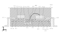
An
図8には、第2半導体チップ32が上面(Z方向の正の方向の面)から下面(Z方向の負の方向の面)へと、もしくはその逆向きに電気信号を伝達するように電極を備えている例を示している。
Figure 8 shows an example in which the
第1フレキシブルプリント配線板12の下面には第1コイル21が形成され、上面には第2コイル22が形成される。第2コイル22の上に、第2コイル22と電気的に接続された電極パッド59が設けられる。電極パッド59に接続されたワイヤW0の他端は、第2半導体チップ32の上面へと接続される。ワイヤW0はワイヤボンディングにより電極パッド59へと接続される。
A
なお、電極パッド59は、例えばXY平面内で複数設けられており、第2コイル22の中心部と外縁部のそれぞれに接続され、ワイヤW0も複数設けられる。
Note that
第3実施形態の第1変形例に係るアイソレータ301によれば、半導体チップ(例えば第2半導体チップ32)の上面とコイル(例えば第2コイル22)との間の電気的接続をワイヤボンディングによって行う際に、基板10の変形を抑制することができる。基板10は、FPC基板である第1フレキシブルプリント配線板12の下に、リジッド基板である第1リジッド基板11を有しており、第1フレキシブルプリント配線板12の変形を抑制することができる。アイソレータ301の信頼性を向上することができる。
According to the
(第4実施形態)
図9は、第4実施形態に係るアイソレータ400の断面構造を表している。第1実施形態に係るアイソレータ100と共通する部分については一部説明を省略する。
Fourth Embodiment
9 shows a cross-sectional structure of an isolator 400 according to the fourth embodiment. Description of some parts common to the
アイソレータ400は、第1ダイパッド81の上に第1半導体チップを有する。また、第2ダイパッド82の上に基板10を有する。第3ダイパッド83の上に第2半導体チップ32を有する。第1ダイパッド81、第2ダイパッド82及び第3ダイパッド83は、それぞれ離間して設けられる。
The isolator 400 has a first semiconductor chip on a first die pad 81. It also has a
第1半導体チップ31は、上面に電極を有しており、第1ダイパッド81と接する下面においては、第1ダイパッド81と電気的に絶縁される。第2半導体チップ32は、上面に電極を有しており、第3ダイパッド83と接する下面においては、第3ダイパッド83と電気的に絶縁される。
The
基板10は、後述するように内部にコイルを含む配線が施されており、配線の一部は第2ダイパッド82と電気的に接続される。
The
第1半導体チップ31と第2ダイパッド82は、ワイヤW1を介して接続される。ワイヤW1は、第1半導体チップ31の上面と、第2ダイパッド82の上面に接する。基板10と第2半導体チップ32は、ワイヤW2を介して接続される。
The
基板10は、第1リジッド基板11及び第1フレキシブルプリント配線板12が積層された2層構造を有する。第1リジッド基板11はリジッド基板である。第1フレキシブルプリント配線板12はFPC基板である。図9に示した例では、第1リジッド基板11は第1フレキシブルプリント配線板12の上に設けられる。
The
第1フレキシブルプリント配線板12には第1コイル21及び第2コイル22が設けられる。第1フレキシブルプリント配線板12の内部構造は、例えば図4に示す例と同様であってもよい。第1コイル21は第1フレキシブルプリント配線板12の下面に設けられ、第2コイル22は第1フレキシブルプリント配線板12の上面に設けられる。第1コイル21は第2ダイパッド82と電気的に接続される。第2コイル22は第1コイル21と電気的に絶縁される。
The first flexible printed
第2コイル22と接続された第3配線43が第1リジッド基板11をZ方向に貫通するように設けられる。第3配線43は第1リジッド基板の上面に設けられた電極パッド59と接続される。電極パッド59には、ワイヤW2が接続される。
The third wiring 43 connected to the
また、アイソレータ400は、外部端子84及び85を有する。外部端子84と85は、それぞれ第1ダイパッド81、第2ダイパッド82及び第3ダイパッド83と離間して設けられる。外部端子84は、例えば入力端子である。外部端子85は、例えば出力端子である。
The isolator 400 also has
外部端子84と第1半導体チップ31は、ワイヤW3を介して電気的に接続される。外部端子85と第2半導体チップ32は、ワイヤW4を介して電気的に接続される。つまり、第1半導体チップ31は、上面に複数の電極を有しており、一方はワイヤW1により第2ダイパッド82に接続され、他方はワイヤW3により外部端子84に接続される。第2半導体チップ32は、上面に複数の電極を有しており、一方は、ワイヤW2により電極パッド59に接続され、他方はワイヤW4により外部端子85に接続される。
The
次に、アイソレータ400の動作について説明する。外部端子84が入力端子、外部端子85が出力端子である例について述べる。
Next, the operation of the isolator 400 will be described. An example will be described in which the
外部端子84に入力される電気信号は、ワイヤW3を介して第1半導体チップ31に到達する。第1半導体チップ31は受け取った電気信号に所定の処理を施して、ワイヤW1へと出力する。第1半導体チップ31から出た信号は、ワイヤW1から第2ダイパッド82を介して第1コイル21へと達する。
The electrical signal input to the
第1コイル21は受け取った電気信号に応じて磁界を生成する。例えば図9でZ方向の磁界が生成される。Z方向の磁界は、第1コイルとはZ方向に離間した第2コイル22を貫通する。第2コイル22には電磁誘導により電流が流れる。磁界を介して第1コイルと第2コイルの間で信号が伝達される。
The
第2コイル22へと伝達された信号は、第3配線43及び電極パッド59を介してワイヤW2に流れる。ワイヤW2を通って、第2半導体チップ32へと信号が伝達される。第2半導体チップ32は、信号に所定の処理を施してワイヤW4へと出力する。ワイヤW4が外部端子85へと伝える信号が出力信号となる。
The signal transmitted to the
本実施形態に係るアイソレータ400によれば、基板10を薄くしてパッケージを小型化しながら、第1フレキシブルプリント配線板12の変形を抑制し、信頼性を向上することができる。
The isolator 400 according to this embodiment can reduce the thickness of the
基板10は、第1リジッド基板11と第1フレキシブルプリント配線板12の2層構造を有する。第1実施形態に係るアイソレータ100と比較して、基板10の厚さを薄くすることができる。基板10の厚さを薄くすることでパッケージの小型化が可能である。
The
第1リジッド基板11はリジッド基板であり、例えばワイヤW2をワイヤボンディングにより設ける際に第1フレキシブルプリント配線板12の変形を抑制することができる。アイソレータ400の信頼性を向上することができる。
The first
なお、第1リジッド基板11は、第1フレキシブルプリント配線板12よりも小さい面積を有していてもよい。電極パッド59は第1リジッド基板11の上に設けられる。ワイヤW2を電極パッド59に接続するワイヤボンディングの工程において基板10に応力がかかるが、リジッド基板である第1リジッド基板11が少なくとも電極パッド59の下に位置していることで、ワイヤW2実装時の応力は第1リジッド基板11に分散することができる。第1リジッド基板11を構成する材料をより少なくすることで、製造コストを削減することができる。
The first
以上説明した少なくとも一つの実施形態によれば、基板10がリジッド基板の層とフレキシブルプリント配線板の層の少なくとも2層の構造を有しており、第1コイル21及び第2コイルが配置される第1フレキシブルプリント配線板12の変形を抑制することができる。アイソレータの実装安定性を向上し、故障および不良を抑制することで、アイソレータの信頼性を向上することができる。また、第1フレキシブルプリント配線板12の上下の面にコイルを形成し、第1コイル21と第2コイル22のZ方向の距離を短くすることで、磁気結合係数を高め、信号伝達にかかる性能を向上することができる。さらには、第1半導体チップ31(第2半導体チップ32)と第1コイル21(第2コイル22)を接続する構造について、配線からの磁界の干渉によって信号伝達にかかる特性が悪化することを抑制できる。
According to at least one embodiment described above, the
以上、具体例を参照しつつ実施形態について説明した。しかし、実施形態はこれらの具体例に限定されるものではない。すなわち、これら具体例に、当業者が適宜設計変更を加えたものも、実施形態の特徴を備えている限り、実施形態の範囲に包含される。前述した各具体例が備える各要素およびその配置、材料、条件、形状、サイズなどは、例示したものに限定されるわけではなく適宜変更することができる。 The above describes the embodiments with reference to specific examples. However, the embodiments are not limited to these specific examples. In other words, designs to which a person skilled in the art has made appropriate design changes to these specific examples are also included within the scope of the embodiments as long as they have the characteristics of the embodiments. The elements of each of the above specific examples, as well as their arrangement, materials, conditions, shapes, sizes, etc., are not limited to those exemplified, and can be modified as appropriate.
以上では、コイルを用いるアイソレータについて説明したが、コンデンサーを用いるアイソレータにも適用することが可能である。 The above describes an isolator that uses a coil, but it can also be applied to an isolator that uses a capacitor.
また、前述した各実施形態が備える各要素は、技術的に可能な限りにおいて複合させることができ、これらを組み合わせたものも実施形態の特徴を含む限り実施形態の範囲に包含される。その他、実施形態の思想の範疇において、当業者であれば、各種の変更例および修正例に想到し得るものであり、それら変更例および修正例についても実施形態の範囲に属するものと了解される。 Furthermore, the elements of each of the above-mentioned embodiments can be combined to the extent technically possible, and combinations of these are also included within the scope of the embodiments as long as they include the features of the embodiments. In addition, within the scope of the ideas of the embodiments, a person skilled in the art may come up with various modifications and amendments, and it is understood that these modifications and amendments also fall within the scope of the embodiments.
本発明のいくつかの実施形態を説明したが、これらの実施形態は、例として提示したものであり、発明の範囲を限定することは意図していない。これら新規な実施形態は、その他の様々な形態で実施されることが可能であり、発明の要旨を逸脱しない範囲で、種々の省略、置き換え、変更を行うことができる。これら実施形態やその変形は、発明の範囲や要旨に含まれるとともに、特許請求の範囲に記載された発明とその均等の範囲に含まれる。 Although several embodiments of the present invention have been described, these embodiments are presented as examples and are not intended to limit the scope of the invention. These novel embodiments can be embodied in various other forms, and various omissions, substitutions, and modifications can be made without departing from the gist of the invention. These embodiments and their modifications are included in the scope and gist of the invention, and are included in the scope of the invention and its equivalents described in the claims.
100、101、200、300、301、400、401・・・アイソレータ
11・・・第1リジッド基板
12・・・第1フレキシブルプリント配線板
13・・・第2リジッド基板
21・・・第1コイル
22・・・第2コイル
31・・・第1半導体チップ
32・・・第2半導体チップ
31a、32a・・・接着層
41・・・第1配線
42・・・第2配線
41a・・・第1部分
42a・・・第1部分
43・・・第3配線
51、52、53、54・・・導電層
55、56・・・貫通導電領域
57、58・・・裏面電極
61、62・・・リードフレーム
61a、62a・・・接着層
70・・・樹脂部
81・・・第1ダイパッド
82・・・第2ダイパッド
83・・・第3ダイパッド
84、85・・・外部端子
W0、W1、W2、W3、W4・・・ワイヤ
100, 101, 200, 300, 301, 400, 401... isolator 11... first
Claims (9)
前記第1フレキシブルプリント配線板に設けられた第1コイルと、
前記第1フレキシブルプリント配線板に設けられ、前記第1方向において前記第1コイルと離間し対向する第2コイルと、
前記基板の上に設けられた第1半導体チップと、
前記基板の上に設けられた第2半導体チップと、
前記基板の中に設けられ、前記第1半導体チップと前記第1コイルを接続する第1配線と、
前記基板の中に設けられ、前記第2半導体チップと前記第2コイルを接続する第2配線と、
を有するアイソレータ。 A substrate including a first rigid substrate which is a rigid substrate, and a first flexible printed wiring board which is a flexible printed wiring board laminated on the first rigid substrate in a first direction;
a first coil provided on the first flexible printed wiring board;
a second coil provided on the first flexible printed wiring board and facing the first coil in the first direction and spaced apart from the first coil;
a first semiconductor chip provided on the substrate;
a second semiconductor chip provided on the substrate;
a first wiring provided in the substrate and connecting the first semiconductor chip and the first coil;
a second wiring provided in the substrate and connecting the second semiconductor chip and the second coil;
An isolator having
前記基板は、前記第1フレキシブルプリント配線板の上に設けられた第2リジッド基板をさらに有する、
請求項1に記載のアイソレータ。 the first flexible printed circuit board is provided on the first rigid substrate,
The substrate further includes a second rigid substrate provided on the first flexible printed wiring board.
2. The isolator of claim 1.
請求項2に記載のアイソレータ。 the first wiring extends in the first direction from an upper surface of the second rigid substrate to a lower surface of the first flexible printed wiring board;
The isolator of claim 2 .
請求項3に記載のアイソレータ。 the first wiring is formed on the first flexible printed wiring board, extends along a lower surface of the first flexible printed wiring board, and has a first portion connected to the first coil;
The isolator of claim 3 .
前記第1半導体チップ又は前記第2半導体チップとそれぞれ電気的に接続される複数のリードフレームと、
をさらに有する、
請求項3に記載のアイソレータ。 a resin portion that seals the first semiconductor chip and the second semiconductor chip;
a plurality of lead frames electrically connected to the first semiconductor chip or the second semiconductor chip,
Further comprising
The isolator of claim 3 .
前記第1リジッド基板に設けられ、前記樹脂部から露出する複数の裏面電極と、
前記基板の中を前記第1方向に延伸して設けられた貫通導電領域と、
前記貫通導電領域と、前記第1半導体チップ又は前記第2半導体チップを接続する導電層と、
をさらに有する、請求項3に記載のアイソレータ。 a resin portion that seals the first semiconductor chip and the second semiconductor chip;
a plurality of back electrodes provided on the first rigid substrate and exposed from the resin portion;
a through conductive region extending in the first direction through the substrate;
a conductive layer connecting the through conductive region and the first semiconductor chip or the second semiconductor chip;
4. The isolator of claim 3 further comprising:
前記第1ダイパッドの上に設けられた第1半導体チップと、
前記第1ダイパッドと離間して設けられた第2ダイパッドと、
前記第2ダイパッドの上に設けられ、リジッド基板である第1リジッド基板と、前記第1リジッド基板に第1方向に積層されたフレキシブルプリント配線板である第1フレキシブルプリント配線板と、を有する基板と、
前記第1フレキシブルプリント配線板に設けられた第1コイルと、
前記第1フレキシブルプリント配線板に設けられ、前記第1方向において前記第1コイルと離間し対向する第2コイルと、
前記基板の上に設けられ、前記基板の中に設けられた第3配線によって前記第2コイルと接続された電極パッドと、
前記第1ダイパッド及び前記第2ダイパッドと離間して設けられた第3ダイパッドと、
前記第3ダイパッドの上に設けられた第2半導体チップと、
前記第1半導体チップと、前記第2ダイパッドとを接続する第1ワイヤと、
前記電極パッドと、前記第2半導体チップとを接続する第2ワイヤと、
を有するアイソレータ。 A first die pad;
a first semiconductor chip provided on the first die pad;
a second die pad spaced apart from the first die pad;
a substrate provided on the second die pad, the substrate including a first rigid substrate which is a rigid substrate, and a first flexible printed wiring board which is a flexible printed wiring board laminated on the first rigid substrate in a first direction;
a first coil provided on the first flexible printed wiring board;
a second coil provided on the first flexible printed wiring board and facing the first coil in the first direction and spaced apart from the first coil;
an electrode pad provided on the substrate and connected to the second coil by a third wiring provided in the substrate;
a third die pad provided spaced apart from the first die pad and the second die pad;
a second semiconductor chip provided on the third die pad;
a first wire connecting the first semiconductor chip and the second die pad;
a second wire connecting the electrode pad and the second semiconductor chip;
An isolator having
前記第1コイルが下面に設けられ、前記第2コイルが上面に設けられる基材と、
前記基材を前記第1方向に挟むように、上面と下面のそれぞれに前記第1コイル又は前記第2コイルの前記第1方向の厚さと同等以上の厚さで設けられた絶縁体と、を有する、
請求項1乃至7のいずれか1項に記載のアイソレータ。 The first flexible printed wiring board is
a substrate having the first coil provided on a lower surface and the second coil provided on an upper surface;
and an insulator having a thickness equal to or greater than a thickness of the first coil or the second coil in the first direction, the insulator being provided on each of an upper surface and a lower surface of the base material so as to sandwich the base material in the first direction.
8. An isolator according to any one of claims 1 to 7.
前記絶縁体は、熱硬化性樹脂を含む、
請求項8に記載のアイソレータ。 the substrate is made of a film-like insulating material containing polyimide;
The insulator includes a thermosetting resin.
9. The isolator of claim 8.
Priority Applications (3)
| Application Number | Priority Date | Filing Date | Title |
|---|---|---|---|
| JP2024020877A JP7686817B1 (en) | 2024-02-15 | 2024-02-15 | Isolator |
| CN202411003168.8A CN120497253A (en) | 2024-02-15 | 2024-07-25 | Isolator |
| US18/815,554 US20250266409A1 (en) | 2024-02-15 | 2024-08-26 | Isolator |
Applications Claiming Priority (1)
| Application Number | Priority Date | Filing Date | Title |
|---|---|---|---|
| JP2024020877A JP7686817B1 (en) | 2024-02-15 | 2024-02-15 | Isolator |
Publications (2)
| Publication Number | Publication Date |
|---|---|
| JP7686817B1 true JP7686817B1 (en) | 2025-06-02 |
| JP2025125043A JP2025125043A (en) | 2025-08-27 |
Family
ID=95895103
Family Applications (1)
| Application Number | Title | Priority Date | Filing Date |
|---|---|---|---|
| JP2024020877A Active JP7686817B1 (en) | 2024-02-15 | 2024-02-15 | Isolator |
Country Status (3)
| Country | Link |
|---|---|
| US (1) | US20250266409A1 (en) |
| JP (1) | JP7686817B1 (en) |
| CN (1) | CN120497253A (en) |
Families Citing this family (1)
| Publication number | Priority date | Publication date | Assignee | Title |
|---|---|---|---|---|
| JP7170685B2 (en) * | 2020-03-19 | 2022-11-14 | 株式会社東芝 | isolator |
Citations (6)
| Publication number | Priority date | Publication date | Assignee | Title |
|---|---|---|---|---|
| JP2007240404A (en) | 2006-03-10 | 2007-09-20 | Nippon Soken Inc | Motion detector |
| JP2012182740A (en) | 2011-03-02 | 2012-09-20 | Nitto Denko Corp | Circuit board for isolator, isolator, and manufacturing method of circuit board and isolator |
| WO2016148113A1 (en) | 2015-03-18 | 2016-09-22 | タツタ電線株式会社 | Stretchable cable and stretchable circuit board |
| JP2022543053A (en) | 2019-08-20 | 2022-10-07 | ステムコ カンパニー リミテッド | Coil device |
| JP2023141929A (en) | 2022-03-24 | 2023-10-05 | 株式会社東芝 | isolator |
| JP2023143993A (en) | 2020-03-19 | 2023-10-06 | 株式会社東芝 | isolator |
-
2024
- 2024-02-15 JP JP2024020877A patent/JP7686817B1/en active Active
- 2024-07-25 CN CN202411003168.8A patent/CN120497253A/en active Pending
- 2024-08-26 US US18/815,554 patent/US20250266409A1/en active Pending
Patent Citations (6)
| Publication number | Priority date | Publication date | Assignee | Title |
|---|---|---|---|---|
| JP2007240404A (en) | 2006-03-10 | 2007-09-20 | Nippon Soken Inc | Motion detector |
| JP2012182740A (en) | 2011-03-02 | 2012-09-20 | Nitto Denko Corp | Circuit board for isolator, isolator, and manufacturing method of circuit board and isolator |
| WO2016148113A1 (en) | 2015-03-18 | 2016-09-22 | タツタ電線株式会社 | Stretchable cable and stretchable circuit board |
| JP2022543053A (en) | 2019-08-20 | 2022-10-07 | ステムコ カンパニー リミテッド | Coil device |
| JP2023143993A (en) | 2020-03-19 | 2023-10-06 | 株式会社東芝 | isolator |
| JP2023141929A (en) | 2022-03-24 | 2023-10-05 | 株式会社東芝 | isolator |
Also Published As
| Publication number | Publication date |
|---|---|
| CN120497253A (en) | 2025-08-15 |
| JP2025125043A (en) | 2025-08-27 |
| US20250266409A1 (en) | 2025-08-21 |
Similar Documents
| Publication | Publication Date | Title |
|---|---|---|
| US7372131B2 (en) | Routing element for use in semiconductor device assemblies | |
| KR20010086344A (en) | Laminate type semiconductor apparatus | |
| US8981579B2 (en) | Impedance controlled packages with metal sheet or 2-layer rdl | |
| KR100606295B1 (en) | Circuit module | |
| JPWO2007086481A1 (en) | Electronic device packages, modules, and electronic equipment | |
| CN100505242C (en) | Multi-level semiconductor micro-module | |
| US12101884B2 (en) | Isolator | |
| WO2018235715A1 (en) | Module and method of manufacturing the same | |
| JP7686817B1 (en) | Isolator | |
| KR101139084B1 (en) | Multilayer printed circuit board and method of making same | |
| JP4071782B2 (en) | Semiconductor device | |
| JPH02343A (en) | Substrate for mounting electronic parts | |
| US20240321850A1 (en) | Isolator | |
| JP7788972B2 (en) | Isolator | |
| US20260082954A1 (en) | Isolator | |
| KR20210062130A (en) | Semiconductor package | |
| JP2026054864A (en) | Isolator | |
| JPWO2012086107A1 (en) | Electronic component mounting structure intermediate, electronic component mounting structure, and method of manufacturing electronic component mounting structure | |
| JP2009231480A (en) | Semiconductor device | |
| JP2009218390A (en) | Semiconductor device, and manufacturing method thereof | |
| CN118693061A (en) | Isolator | |
| JPH11176975A (en) | Semiconductor device |
Legal Events
| Date | Code | Title | Description |
|---|---|---|---|
| A621 | Written request for application examination |
Free format text: JAPANESE INTERMEDIATE CODE: A621 Effective date: 20240520 |
|
| RD07 | Notification of extinguishment of power of attorney |
Free format text: JAPANESE INTERMEDIATE CODE: A7427 Effective date: 20250321 |
|
| TRDD | Decision of grant or rejection written | ||
| A01 | Written decision to grant a patent or to grant a registration (utility model) |
Free format text: JAPANESE INTERMEDIATE CODE: A01 Effective date: 20250422 |
|
| A61 | First payment of annual fees (during grant procedure) |
Free format text: JAPANESE INTERMEDIATE CODE: A61 Effective date: 20250521 |
|
| R150 | Certificate of patent or registration of utility model |
Ref document number: 7686817 Country of ref document: JP Free format text: JAPANESE INTERMEDIATE CODE: R150 |