JP7660552B2 - Light emitting device and method for manufacturing the same - Google Patents
Light emitting device and method for manufacturing the same Download PDFInfo
- Publication number
- JP7660552B2 JP7660552B2 JP2022501777A JP2022501777A JP7660552B2 JP 7660552 B2 JP7660552 B2 JP 7660552B2 JP 2022501777 A JP2022501777 A JP 2022501777A JP 2022501777 A JP2022501777 A JP 2022501777A JP 7660552 B2 JP7660552 B2 JP 7660552B2
- Authority
- JP
- Japan
- Prior art keywords
- layer
- light
- based semiconductor
- arsenic
- semiconductor
- Prior art date
- Legal status (The legal status is an assumption and is not a legal conclusion. Google has not performed a legal analysis and makes no representation as to the accuracy of the status listed.)
- Active
Links
Images


Classifications
-
- H—ELECTRICITY
- H01—ELECTRIC ELEMENTS
- H01S—DEVICES USING THE PROCESS OF LIGHT AMPLIFICATION BY STIMULATED EMISSION OF RADIATION [LASER] TO AMPLIFY OR GENERATE LIGHT; DEVICES USING STIMULATED EMISSION OF ELECTROMAGNETIC RADIATION IN WAVE RANGES OTHER THAN OPTICAL
- H01S5/00—Semiconductor lasers
- H01S5/40—Arrangement of two or more semiconductor lasers, not provided for in groups H01S5/02 - H01S5/30
- H01S5/42—Arrays of surface emitting lasers
- H01S5/423—Arrays of surface emitting lasers having a vertical cavity
-
- H—ELECTRICITY
- H01—ELECTRIC ELEMENTS
- H01S—DEVICES USING THE PROCESS OF LIGHT AMPLIFICATION BY STIMULATED EMISSION OF RADIATION [LASER] TO AMPLIFY OR GENERATE LIGHT; DEVICES USING STIMULATED EMISSION OF ELECTROMAGNETIC RADIATION IN WAVE RANGES OTHER THAN OPTICAL
- H01S5/00—Semiconductor lasers
- H01S5/10—Construction or shape of the optical resonator, e.g. extended or external cavity, coupled cavities, bent-guide, varying width, thickness or composition of the active region
- H01S5/18—Surface-emitting [SE] lasers, e.g. having both horizontal and vertical cavities
- H01S5/183—Surface-emitting [SE] lasers, e.g. having both horizontal and vertical cavities having only vertical cavities, e.g. vertical cavity surface-emitting lasers [VCSEL]
- H01S5/18305—Surface-emitting [SE] lasers, e.g. having both horizontal and vertical cavities having only vertical cavities, e.g. vertical cavity surface-emitting lasers [VCSEL] with emission through the substrate, i.e. bottom emission
-
- H—ELECTRICITY
- H01—ELECTRIC ELEMENTS
- H01S—DEVICES USING THE PROCESS OF LIGHT AMPLIFICATION BY STIMULATED EMISSION OF RADIATION [LASER] TO AMPLIFY OR GENERATE LIGHT; DEVICES USING STIMULATED EMISSION OF ELECTROMAGNETIC RADIATION IN WAVE RANGES OTHER THAN OPTICAL
- H01S5/00—Semiconductor lasers
- H01S5/10—Construction or shape of the optical resonator, e.g. extended or external cavity, coupled cavities, bent-guide, varying width, thickness or composition of the active region
- H01S5/18—Surface-emitting [SE] lasers, e.g. having both horizontal and vertical cavities
- H01S5/183—Surface-emitting [SE] lasers, e.g. having both horizontal and vertical cavities having only vertical cavities, e.g. vertical cavity surface-emitting lasers [VCSEL]
- H01S5/18361—Structure of the reflectors, e.g. hybrid mirrors
-
- H—ELECTRICITY
- H01—ELECTRIC ELEMENTS
- H01S—DEVICES USING THE PROCESS OF LIGHT AMPLIFICATION BY STIMULATED EMISSION OF RADIATION [LASER] TO AMPLIFY OR GENERATE LIGHT; DEVICES USING STIMULATED EMISSION OF ELECTROMAGNETIC RADIATION IN WAVE RANGES OTHER THAN OPTICAL
- H01S5/00—Semiconductor lasers
- H01S5/10—Construction or shape of the optical resonator, e.g. extended or external cavity, coupled cavities, bent-guide, varying width, thickness or composition of the active region
- H01S5/18—Surface-emitting [SE] lasers, e.g. having both horizontal and vertical cavities
- H01S5/183—Surface-emitting [SE] lasers, e.g. having both horizontal and vertical cavities having only vertical cavities, e.g. vertical cavity surface-emitting lasers [VCSEL]
- H01S5/18386—Details of the emission surface for influencing the near- or far-field, e.g. a grating on the surface
- H01S5/18394—Apertures, e.g. defined by the shape of the upper electrode
-
- G—PHYSICS
- G01—MEASURING; TESTING
- G01S—RADIO DIRECTION-FINDING; RADIO NAVIGATION; DETERMINING DISTANCE OR VELOCITY BY USE OF RADIO WAVES; LOCATING OR PRESENCE-DETECTING BY USE OF THE REFLECTION OR RERADIATION OF RADIO WAVES; ANALOGOUS ARRANGEMENTS USING OTHER WAVES
- G01S7/00—Details of systems according to groups G01S13/00, G01S15/00, G01S17/00
- G01S7/48—Details of systems according to groups G01S13/00, G01S15/00, G01S17/00 of systems according to group G01S17/00
- G01S7/481—Constructional features, e.g. arrangements of optical elements
- G01S7/4814—Constructional features, e.g. arrangements of optical elements of transmitters alone
-
- H—ELECTRICITY
- H01—ELECTRIC ELEMENTS
- H01S—DEVICES USING THE PROCESS OF LIGHT AMPLIFICATION BY STIMULATED EMISSION OF RADIATION [LASER] TO AMPLIFY OR GENERATE LIGHT; DEVICES USING STIMULATED EMISSION OF ELECTROMAGNETIC RADIATION IN WAVE RANGES OTHER THAN OPTICAL
- H01S2301/00—Functional characteristics
- H01S2301/17—Semiconductor lasers comprising special layers
- H01S2301/173—The laser chip comprising special buffer layers, e.g. dislocation prevention or reduction
-
- H—ELECTRICITY
- H01—ELECTRIC ELEMENTS
- H01S—DEVICES USING THE PROCESS OF LIGHT AMPLIFICATION BY STIMULATED EMISSION OF RADIATION [LASER] TO AMPLIFY OR GENERATE LIGHT; DEVICES USING STIMULATED EMISSION OF ELECTROMAGNETIC RADIATION IN WAVE RANGES OTHER THAN OPTICAL
- H01S2301/00—Functional characteristics
- H01S2301/17—Semiconductor lasers comprising special layers
- H01S2301/176—Specific passivation layers on surfaces other than the emission facet
-
- H—ELECTRICITY
- H01—ELECTRIC ELEMENTS
- H01S—DEVICES USING THE PROCESS OF LIGHT AMPLIFICATION BY STIMULATED EMISSION OF RADIATION [LASER] TO AMPLIFY OR GENERATE LIGHT; DEVICES USING STIMULATED EMISSION OF ELECTROMAGNETIC RADIATION IN WAVE RANGES OTHER THAN OPTICAL
- H01S5/00—Semiconductor lasers
- H01S5/04—Processes or apparatus for excitation, e.g. pumping, e.g. by electron beams
- H01S5/042—Electrical excitation ; Circuits therefor
- H01S5/0425—Electrodes, e.g. characterised by the structure
- H01S5/04256—Electrodes, e.g. characterised by the structure characterised by the configuration
- H01S5/04257—Electrodes, e.g. characterised by the structure characterised by the configuration having positive and negative electrodes on the same side of the substrate
-
- H—ELECTRICITY
- H01—ELECTRIC ELEMENTS
- H01S—DEVICES USING THE PROCESS OF LIGHT AMPLIFICATION BY STIMULATED EMISSION OF RADIATION [LASER] TO AMPLIFY OR GENERATE LIGHT; DEVICES USING STIMULATED EMISSION OF ELECTROMAGNETIC RADIATION IN WAVE RANGES OTHER THAN OPTICAL
- H01S5/00—Semiconductor lasers
- H01S5/10—Construction or shape of the optical resonator, e.g. extended or external cavity, coupled cavities, bent-guide, varying width, thickness or composition of the active region
- H01S5/18—Surface-emitting [SE] lasers, e.g. having both horizontal and vertical cavities
- H01S5/183—Surface-emitting [SE] lasers, e.g. having both horizontal and vertical cavities having only vertical cavities, e.g. vertical cavity surface-emitting lasers [VCSEL]
- H01S5/18308—Surface-emitting [SE] lasers, e.g. having both horizontal and vertical cavities having only vertical cavities, e.g. vertical cavity surface-emitting lasers [VCSEL] having a special structure for lateral current or light confinement
- H01S5/18311—Surface-emitting [SE] lasers, e.g. having both horizontal and vertical cavities having only vertical cavities, e.g. vertical cavity surface-emitting lasers [VCSEL] having a special structure for lateral current or light confinement using selective oxidation
-
- H—ELECTRICITY
- H01—ELECTRIC ELEMENTS
- H01S—DEVICES USING THE PROCESS OF LIGHT AMPLIFICATION BY STIMULATED EMISSION OF RADIATION [LASER] TO AMPLIFY OR GENERATE LIGHT; DEVICES USING STIMULATED EMISSION OF ELECTROMAGNETIC RADIATION IN WAVE RANGES OTHER THAN OPTICAL
- H01S5/00—Semiconductor lasers
- H01S5/10—Construction or shape of the optical resonator, e.g. extended or external cavity, coupled cavities, bent-guide, varying width, thickness or composition of the active region
- H01S5/18—Surface-emitting [SE] lasers, e.g. having both horizontal and vertical cavities
- H01S5/183—Surface-emitting [SE] lasers, e.g. having both horizontal and vertical cavities having only vertical cavities, e.g. vertical cavity surface-emitting lasers [VCSEL]
- H01S5/18308—Surface-emitting [SE] lasers, e.g. having both horizontal and vertical cavities having only vertical cavities, e.g. vertical cavity surface-emitting lasers [VCSEL] having a special structure for lateral current or light confinement
- H01S5/18322—Position of the structure
- H01S5/18325—Between active layer and substrate
-
- H—ELECTRICITY
- H01—ELECTRIC ELEMENTS
- H01S—DEVICES USING THE PROCESS OF LIGHT AMPLIFICATION BY STIMULATED EMISSION OF RADIATION [LASER] TO AMPLIFY OR GENERATE LIGHT; DEVICES USING STIMULATED EMISSION OF ELECTROMAGNETIC RADIATION IN WAVE RANGES OTHER THAN OPTICAL
- H01S5/00—Semiconductor lasers
- H01S5/10—Construction or shape of the optical resonator, e.g. extended or external cavity, coupled cavities, bent-guide, varying width, thickness or composition of the active region
- H01S5/18—Surface-emitting [SE] lasers, e.g. having both horizontal and vertical cavities
- H01S5/183—Surface-emitting [SE] lasers, e.g. having both horizontal and vertical cavities having only vertical cavities, e.g. vertical cavity surface-emitting lasers [VCSEL]
- H01S5/18344—Surface-emitting [SE] lasers, e.g. having both horizontal and vertical cavities having only vertical cavities, e.g. vertical cavity surface-emitting lasers [VCSEL] characterized by the mesa, e.g. dimensions or shape of the mesa
- H01S5/18347—Mesa comprising active layer
-
- H—ELECTRICITY
- H01—ELECTRIC ELEMENTS
- H01S—DEVICES USING THE PROCESS OF LIGHT AMPLIFICATION BY STIMULATED EMISSION OF RADIATION [LASER] TO AMPLIFY OR GENERATE LIGHT; DEVICES USING STIMULATED EMISSION OF ELECTROMAGNETIC RADIATION IN WAVE RANGES OTHER THAN OPTICAL
- H01S5/00—Semiconductor lasers
- H01S5/30—Structure or shape of the active region; Materials used for the active region
- H01S5/305—Structure or shape of the active region; Materials used for the active region characterised by the doping materials used in the laser structure
-
- H—ELECTRICITY
- H01—ELECTRIC ELEMENTS
- H01S—DEVICES USING THE PROCESS OF LIGHT AMPLIFICATION BY STIMULATED EMISSION OF RADIATION [LASER] TO AMPLIFY OR GENERATE LIGHT; DEVICES USING STIMULATED EMISSION OF ELECTROMAGNETIC RADIATION IN WAVE RANGES OTHER THAN OPTICAL
- H01S5/00—Semiconductor lasers
- H01S5/30—Structure or shape of the active region; Materials used for the active region
- H01S5/34—Structure or shape of the active region; Materials used for the active region comprising quantum well or superlattice structures, e.g. single quantum well [SQW] lasers, multiple quantum well [MQW] lasers or graded index separate confinement heterostructure [GRINSCH] lasers
- H01S5/343—Structure or shape of the active region; Materials used for the active region comprising quantum well or superlattice structures, e.g. single quantum well [SQW] lasers, multiple quantum well [MQW] lasers or graded index separate confinement heterostructure [GRINSCH] lasers in AIIIBV compounds, e.g. AlGaAs-laser, InP-based laser
- H01S5/34313—Structure or shape of the active region; Materials used for the active region comprising quantum well or superlattice structures, e.g. single quantum well [SQW] lasers, multiple quantum well [MQW] lasers or graded index separate confinement heterostructure [GRINSCH] lasers in AIIIBV compounds, e.g. AlGaAs-laser, InP-based laser with a well layer having only As as V-compound, e.g. AlGaAs, InGaAs
- H01S5/3432—Structure or shape of the active region; Materials used for the active region comprising quantum well or superlattice structures, e.g. single quantum well [SQW] lasers, multiple quantum well [MQW] lasers or graded index separate confinement heterostructure [GRINSCH] lasers in AIIIBV compounds, e.g. AlGaAs-laser, InP-based laser with a well layer having only As as V-compound, e.g. AlGaAs, InGaAs the whole junction comprising only (AI)GaAs
-
- H—ELECTRICITY
- H10—SEMICONDUCTOR DEVICES; ELECTRIC SOLID-STATE DEVICES NOT OTHERWISE PROVIDED FOR
- H10P—GENERIC PROCESSES OR APPARATUS FOR THE MANUFACTURE OR TREATMENT OF DEVICES COVERED BY CLASS H10
- H10P14/00—Formation of materials, e.g. in the shape of layers or pillars
- H10P14/20—Formation of materials, e.g. in the shape of layers or pillars of semiconductor materials
- H10P14/24—Formation of materials, e.g. in the shape of layers or pillars of semiconductor materials using chemical vapour deposition [CVD]
-
- H—ELECTRICITY
- H10—SEMICONDUCTOR DEVICES; ELECTRIC SOLID-STATE DEVICES NOT OTHERWISE PROVIDED FOR
- H10P—GENERIC PROCESSES OR APPARATUS FOR THE MANUFACTURE OR TREATMENT OF DEVICES COVERED BY CLASS H10
- H10P14/00—Formation of materials, e.g. in the shape of layers or pillars
- H10P14/20—Formation of materials, e.g. in the shape of layers or pillars of semiconductor materials
- H10P14/34—Deposited materials, e.g. layers
- H10P14/3402—Deposited materials, e.g. layers characterised by the chemical composition
- H10P14/3414—Deposited materials, e.g. layers characterised by the chemical composition being group IIIA-VIA materials
- H10P14/3418—Phosphides
-
- H—ELECTRICITY
- H10—SEMICONDUCTOR DEVICES; ELECTRIC SOLID-STATE DEVICES NOT OTHERWISE PROVIDED FOR
- H10P—GENERIC PROCESSES OR APPARATUS FOR THE MANUFACTURE OR TREATMENT OF DEVICES COVERED BY CLASS H10
- H10P14/00—Formation of materials, e.g. in the shape of layers or pillars
- H10P14/20—Formation of materials, e.g. in the shape of layers or pillars of semiconductor materials
- H10P14/34—Deposited materials, e.g. layers
- H10P14/3402—Deposited materials, e.g. layers characterised by the chemical composition
- H10P14/3414—Deposited materials, e.g. layers characterised by the chemical composition being group IIIA-VIA materials
- H10P14/3421—Arsenides
-
- H—ELECTRICITY
- H10—SEMICONDUCTOR DEVICES; ELECTRIC SOLID-STATE DEVICES NOT OTHERWISE PROVIDED FOR
- H10P—GENERIC PROCESSES OR APPARATUS FOR THE MANUFACTURE OR TREATMENT OF DEVICES COVERED BY CLASS H10
- H10P14/00—Formation of materials, e.g. in the shape of layers or pillars
- H10P14/20—Formation of materials, e.g. in the shape of layers or pillars of semiconductor materials
- H10P14/34—Deposited materials, e.g. layers
- H10P14/3438—Doping during depositing
- H10P14/3441—Conductivity type
- H10P14/3442—N-type
-
- H—ELECTRICITY
- H10—SEMICONDUCTOR DEVICES; ELECTRIC SOLID-STATE DEVICES NOT OTHERWISE PROVIDED FOR
- H10P—GENERIC PROCESSES OR APPARATUS FOR THE MANUFACTURE OR TREATMENT OF DEVICES COVERED BY CLASS H10
- H10P14/00—Formation of materials, e.g. in the shape of layers or pillars
- H10P14/20—Formation of materials, e.g. in the shape of layers or pillars of semiconductor materials
- H10P14/34—Deposited materials, e.g. layers
- H10P14/3438—Doping during depositing
- H10P14/3441—Conductivity type
- H10P14/3444—P-type
-
- H—ELECTRICITY
- H10—SEMICONDUCTOR DEVICES; ELECTRIC SOLID-STATE DEVICES NOT OTHERWISE PROVIDED FOR
- H10P—GENERIC PROCESSES OR APPARATUS FOR THE MANUFACTURE OR TREATMENT OF DEVICES COVERED BY CLASS H10
- H10P14/00—Formation of materials, e.g. in the shape of layers or pillars
- H10P14/20—Formation of materials, e.g. in the shape of layers or pillars of semiconductor materials
- H10P14/34—Deposited materials, e.g. layers
- H10P14/3438—Doping during depositing
- H10P14/3441—Conductivity type
- H10P14/3446—Transition metal elements; Rare earth elements
Landscapes
- Physics & Mathematics (AREA)
- Condensed Matter Physics & Semiconductors (AREA)
- General Physics & Mathematics (AREA)
- Electromagnetism (AREA)
- Optics & Photonics (AREA)
- Semiconductor Lasers (AREA)
Description
本開示は、発光デバイスおよび発光デバイスの製造方法に関する。 The present disclosure relates to light-emitting devices and methods for manufacturing light-emitting devices.
例えば、特許文献1では、不純物として炭素(C)がドープされたDBR上に、不純物として亜鉛(Zn)がドープされたp形のInGaPからなる保護層を設けることでレーザ発振の安定化を図った面発光レーザが開示されている。For example, Patent Document 1 discloses a surface-emitting laser in which a protective layer made of p-type InGaP doped with zinc (Zn) as an impurity is provided on a DBR doped with carbon (C) as an impurity, thereby stabilizing laser oscillation.
ところで、発光デバイスではデバイス特性の安定性および製造歩留まりの向上が望まれている。However, in light-emitting devices, there is a demand for improved stability of device characteristics and manufacturing yields.
デバイス特性の安定性および製造歩留まりを向上させることが可能な発光デバイスおよび発光デバイスの製造方法を提供することが望ましい。It is desirable to provide a light-emitting device and a method for manufacturing a light-emitting device that can improve the stability of device characteristics and manufacturing yield.
本開示の一実施の形態の発光デバイスは、基板と、基板側から第2の光反射層、活性層および不純物として炭素を含むヒ素系半導体層からなる第1の光反射層の順に積層された半導体積層体と、半導体積層体の第1の光反射層側に設けられ、半導体積層体に面する一の面および一の面とは反対側の他の面を有するリン系半導体層からなる第1のバッファ層と、少なくとも第1の光反射層と第1のバッファ層との間に設けられ、不純物としてマグネシウムを含むヒ素系半導体層からなる第2のバッファ層と、第1のバッファ層の他の面側に設けられると共に、不純物として炭素を含むヒ素系半導体層からなる第1のコンタクト層と、基板と第2の光反射層との間に設けられた第2のコンタクト層とを備えたものであり、第2のバッファ層は、第1のバッファ層の一の面および他の面の両方に設けられ、第1のコンタクト層および第1のバッファ層の他の面側に設けられた第2のバッファ層に光出射面となる開口が形成されている。 A light-emitting device according to an embodiment of the present disclosure includes a substrate, a semiconductor laminate including a second light-reflecting layer , an active layer, and a first light-reflecting layer including an arsenic-based semiconductor layer including carbon as an impurity, laminated in this order from the substrate side, a first buffer layer provided on the first light-reflecting layer side of the semiconductor laminate and including a phosphorus-based semiconductor layer having one surface facing the semiconductor laminate and another surface opposite to the first surface, a second buffer layer provided at least between the first light-reflecting layer and the first buffer layer and including an arsenic-based semiconductor layer including magnesium as an impurity, a first contact layer provided on the other surface side of the first buffer layer and including an arsenic-based semiconductor layer including carbon as an impurity, and a second contact layer provided between the substrate and the second light-reflecting layer, the second buffer layer being provided on both the one surface and the other surface of the first buffer layer, and an opening serving as a light emission surface is formed in the second buffer layer provided on the first contact layer and the other surface side of the first buffer layer .
本開示の一実施形態の発光デバイスの製造方法は、基板上に第2のコンタクト層、第2の光反射層、活性層、不純物として炭素を含むヒ素系半導体層からなる第1の光反射層、不純物として亜鉛またはマグネシウムを含むヒ素系半導体層からなる第2のバッファ層、リン系半導体層からなる第1のバッファ層、第2のバッファ層および不純物として炭素を含むヒ素系半導体層からなる第1のコンタクト層を結晶成長によりこの順に形成した後、第1のバッファ層をエッチングストップ層として第1のコンタクト層および第2のバッファ層をエッチングして、底面が光出射面となる開口を形成する。 A method for manufacturing a light-emitting device according to an embodiment of the present disclosure includes forming, in this order on a substrate by crystal growth, a second contact layer, a second light-reflecting layer, an active layer, a first light-reflecting layer made of an arsenic-based semiconductor layer containing carbon as an impurity , a second buffer layer made of an arsenic-based semiconductor layer containing zinc or magnesium as an impurity, a first buffer layer made of a phosphorus-based semiconductor layer, the second buffer layer, and a first contact layer made of an arsenic-based semiconductor layer containing carbon as an impurity, and then etching the first contact layer and the second buffer layer using the first buffer layer as an etching stop layer to form an opening whose bottom surface serves as a light-emitting surface.
本開示の一実施の形態の発光デバイス、一実施の形態の第1の発光デバイスの製造方法および一実施形態の第2の発光デバイスの製造方法では、半導体積層体を構成する、不純物として炭素を含むヒ素系半導体層からなる第1の光反射層と、リン系半導体層からなる第1のバッファ層との間に、不純物として亜鉛またはマグネシウムを含むヒ素系半導体層からなる第2のバッファ層を設けるようにした。これにより、第1の光反射層に不純物として含まれる炭素の原料とリン系半導体との接触による結晶成長面の表面状態の悪化を抑制する。In the light-emitting device according to an embodiment of the present disclosure, the manufacturing method of the first light-emitting device according to an embodiment, and the manufacturing method of the second light-emitting device according to an embodiment, a second buffer layer made of an arsenic-based semiconductor layer containing zinc or magnesium as an impurity is provided between a first light-reflecting layer made of an arsenic-based semiconductor layer containing carbon as an impurity and a first buffer layer made of a phosphorus-based semiconductor layer, which constitute a semiconductor laminate. This suppresses deterioration of the surface condition of the crystal growth surface due to contact between the carbon raw material contained as an impurity in the first light-reflecting layer and the phosphorus-based semiconductor.
以下、本開示の実施の形態について、図面を参照して詳細に説明する。以下の説明は本開示の一具体例であって、本開示は以下の態様に限定されるものではない。また、本開示は、各図に示す各構成要素の配置や寸法、寸法比等についても、それらに限定されるものではない。なお、説明する順序は、下記の通りである。
1.第1の実施の形態(Cドープされたヒ素系半導体からなる第1反射層とリン系半導体層からなる第1バッファ層との間に、ZnまたはMgがドープされたヒ素系半導体からなる第2バッファ層を有する裏面出射型の半導体レーザの例)
1-1.半導体レーザの構成
1-2.半導体レーザの製造方法
1-3.作用・効果
2.第2の実施の形態(Cドープされたヒ素系半導体からなる第1反射層とリン系半導体層からなる第1バッファ層との間に、ZnまたはMgがドープされたヒ素系半導体からなる第2バッファ層を有する表面出射型の半導体レーザの例)
3.適用例(測距装置の例)
Hereinafter, an embodiment of the present disclosure will be described in detail with reference to the drawings. The following description is a specific example of the present disclosure, and the present disclosure is not limited to the following embodiment. Furthermore, the present disclosure is not limited to the arrangement, dimensions, dimensional ratios, etc. of each component shown in each drawing. The order of description is as follows.
1. First embodiment (an example of a back-emitting semiconductor laser having a second buffer layer made of an arsenic-based semiconductor doped with Zn or Mg between a first reflective layer made of a C-doped arsenic-based semiconductor and a first buffer layer made of a phosphorus-based semiconductor layer)
1-1. Configuration of the semiconductor laser 1-2. Manufacturing method of the semiconductor laser 1-3. Actions and
3. Application example (example of distance measuring device)
<1.第1の実施の形態>
図1は、本開示の第1の実施の形態に係る発光デバイス(半導体レーザ1)の断面構成の一例を模式的に表したものである。この半導体レーザ1は、例えば、裏面出射型の垂直共振器面発光レーザ(Vertical Cavity Surface Emitting LASER:VCSEL)であり、例えば、複数の発光領域として複数のVCSELがアレイ状に集積されたものである。
1. First embodiment
1 is a schematic diagram showing an example of a cross-sectional configuration of a light-emitting device (semiconductor laser 1) according to a first embodiment of the present disclosure. The semiconductor laser 1 is, for example, a back-emitting vertical cavity surface-emitting laser (VCSEL), and is, for example, an array of multiple VCSELs integrated as multiple light-emitting regions.
(1-1.半導体レーザの構成)
半導体レーザ1は、例えば、基板11の第1面(表面(面11S1))に複数の半導体積層体10を有している。半導体積層体10は、例えば柱状形状(メサ形状)を有し、例えば、第1光反射層14、活性層15および第2光反射層16がこの順に積層されている。第1光反射層14と活性層15との間には、電流注入領域17Aを形成する電流狭窄層17が設けられている。この半導体積層体10が、本開示の「半導体積層体」の一具体例に相当する。半導体積層体10と基板11との間には、第1コンタクト層12およびバッファ層13が基板側から順に積層されており、バッファ層13は、例えば、第1層13A、第2層13Bおよび第3層13Cが、第1コンタクト層12側からこの順に積層された多層構造を有し、半導体積層体10と共に、メサ形状を形成している。第1コンタクト層12は、複数の半導体積層体10に対する共通層として基板11上に延在している。第1コンタクト層12上には、第1電極21が各半導体積層体10の共通電極として設けられている。各半導体積層体10の上面(面10S1)には、それぞれ、第2コンタクト層18および第2電極22がこの順に形成されている。更に、第1電極21および第2電極22を除く第1コンタクト層12の上面(面12S1)および第2コンタクト層18の上面ならびに第2コンタクト層18、半導体積層体10およびバッファ層13の側面は絶縁膜23に覆われており、基板11の第2面(裏面(面11S2))は絶縁膜24に覆われている。
(1-1. Configuration of Semiconductor Laser)
The semiconductor laser 1 has, for example, a plurality of
以下に、半導体レーザ1の各部の構成や材料等について詳細に説明する。 Below, the configuration and materials of each part of the semiconductor laser 1 are explained in detail.
基板11は、複数の半導体積層体10を集積する支持基板である。本実施の形態のように、裏面出射型の半導体レーザ1では、基板11は、例えば不純物を含まない、例えばGaAs系半導体によって構成されている半絶縁性基板を用いることが好ましい。この他、基板11は、キャリア濃度が低く、レーザ光の吸収が低減されるものであればよく、例えば、p型またはn型のキャリア濃度が5×1017cm-3以下のキャリア濃度を有する基板を用いることができる。
The
第1コンタクト層12は、例えばGaAs系半導体によって構成されている。第1コンタクト層12は、第1電極21と各半導体積層体10の第1光反射層14とを電気的に接続するためのものである。第1コンタクト層12は、p型のGaAsによって構成されており、不純物として、例えば炭素(C)を含んでいる。第1コンタクト層12は、本開示の「第1のコンタクト層」の一具体例に相当する。The
バッファ層13は、上記のように、第1層13A、第2層13Bおよび第3層13Cが第1コンタクト層12側からこの順に積層された多層構造を有するものである。第1層13Aは、例えば、不純物として亜鉛(Zn)またはマグネシウム(Mg)を含むヒ素系半導体層によって構成されている。第2層13Bは、例えば、不純物として亜鉛(Zn)またはマグネシウム(Mg)を含むリン系半導体層によって構成されている。第3層13Cは、第1層13Aと同様に、例えば、不純物として亜鉛(Zn)またはマグネシウム(Mg)を含むヒ素系半導体層によって構成されている。As described above, the
ヒ素系半導体層は、少なくともヒ素(As)を含む化合物半導体を含む層であり、例えば、GaAs層、AlGaAs層およびAlAs層が挙げられる。第1層13Aおよび第3層13Cは、本開示の「第2のバッファ層」の一具体例に相当し、上記半導体層のうちのいずれか1層または2層以上からなる単層膜または積層膜として形成することができる。第1層13Aおよび第3層13Cの積層方向の膜厚(以下、単に厚みという)は、例えば5nm以上100nm以下である。The arsenic-based semiconductor layer is a layer containing a compound semiconductor containing at least arsenic (As), and examples thereof include a GaAs layer, an AlGaAs layer, and an AlAs layer. The
リン系半導体層は、少なくともリン(P)を含む化合物半導体を含む層であり、例えば、GaInP層、AlGaInP層およびAlInP層が挙げられる。第2層13Bは、本開示の「第1のバッファ層」の一具体例に相当し、上記半導体層のうちのいずれか1層または2層以上からなる単層膜または積層膜として形成することができる。第2層13Bの厚みは、例えば50nm以上300nm以下である。The phosphorus-based semiconductor layer is a layer containing a compound semiconductor containing at least phosphorus (P), and examples thereof include a GaInP layer, an AlGaInP layer, and an AlInP layer. The
第1光反射層14は、バッファ層13と電流狭窄層17との間に配置され、活性層15および電流狭窄層17を間にして第2光反射層16と対向している。第1光反射層14は、活性層15で発生した光を第2光反射層16との間で共振させるようになっている。第1光反射層14は、本開示の「第1の光反射層」の一具体例に相当する。The first
第1光反射層14は、低屈折率層(図示せず)および高屈折率層(図示せず)を交互に積層したDBR(Distributed Bragg Reflector)層である。低屈折率層は、例えば光学厚さがλ×1/4nのp型のAlx1Ga1-x1As(0<x1≦1)からなり、高屈折率層は、例えば光学厚さがλ×1/4nのp型のAlx2Ga1-x2As(0≦x2<x1)からなる。λは、各発光領域から発せられるレーザ光の発振波長であり、nは、屈折率である。第1光反射層14は、不純物として、例えば炭素(C)を含んでいる。
The first
活性層15は、第1光反射層14と第2光反射層16との間に設けられている。活性層15は、例えばアルミニウムガリウムヒ素(AlGaAs)系の半導体材料により構成されている。活性層15では、第1電極21および第2電極22から注入された正孔および電子が発光再結合して誘導放出光を発生するようになっている。活性層15のうち電流注入領域17Aとの対向領域が発光領域となる。活性層15には、例えばアンドープのAlx3Ga1-x3As(0<x3≦0.45)を用いることができる。活性層15は、例えばGaAsとAlGaAsとの多重量子井戸(MQW:Multi Quantum Well)構造を有していてもよい。この他、インジウムガリウムヒ素(InGaAs)とAlGaAsとの多重量子井戸構造により活性層15を構成するようにしてもよい。活性層15は、本開示の「活性層」の一具体例に相当する。
The
第2光反射層16は、活性層15と第2コンタクト層18との間に配置されたDBR層である。第2光反射層16は、活性層15および電流狭窄層17を間にして第1光反射層14と対向している。第2光反射層16は、本開示の「第2の光反射層」の一具体例に相当する。The second
第2光反射層16は、低屈折率層および高屈折率層を交互に重ねた積層構造を有している。低屈折率層は、例えば光学膜厚がλ/4nのn型のAlx4Ga1-x4As(0<x4≦1)である。高屈折率層は、例えば光学膜厚がλ/4nのn型のAlx5Ga1-x5As(0≦x5<x4)である。第2光反射層16は、不純物として、例えばシリコン(Si)を含んでいる。
The second
電流狭窄層17は、第1光反射層14と活性層15との間に設けられ、例えば、メサ形状を有する半導体積層体10の外周側から内側に所定の幅を有して環状に形成されている。換言すると、電流狭窄層17は、第1光反射層14と活性層15との間に設けられ、その中央部分に所定の幅の開口を有しており、この開口が電流注入領域17Aとなっている。電流狭窄層17は、例えばp型のAlGaAsにより構成されている。具体的には、電流狭窄層17は、Al0.85Ga0.15As~AlAsからなり、これを酸化して酸化アルミニウム(AlOx)層とすることで、電流を狭窄する。半導体レーザ1では、この電流狭窄層17を設けることにより、第1電極21から活性層15に注入させる電流の狭窄がなされ、電流注入効率が高められる。
The
第2コンタクト層18は、導電性を有する、例えばGaAs系半導体によって構成されている。第2コンタクト層18は、例えば、n型のGaAsによって構成されており、不純物として、例えばシリコン(Si)を含んでいる。第2コンタクト層18は、本開示の「第2のコンタクト層」の一具体例に相当する。The
第1電極21は、第1コンタクト層12上に設けられ、例えば、例えば、チタン(Ti)/白金(Pt)/金(Au)の多層膜によって形成されている。The
第2電極22は、半導体積層体10の上方、具体的には、第2コンタクト層18上に設けられ、例えば金-ゲルマニウム(Au-Ge)/ニッケル(Ni)/金(Au)の多層膜によって形成されている。The
絶縁膜23は、第2コンタクト層18の上面および第2コンタクト層18、半導体積層体10およびバッファ層13の側面ならびに第1コンタクト層12の上面(面12S1)に、例えば連続して形成されている。絶縁膜23は、例えば窒化シリコン(SiN)あるいは酸化シリコン(SiO2)等の単層膜または積層膜により構成されている。絶縁膜23の各第2コンタクト層18の上面および第1コンタクト層12の所定の位置は、それぞれ、開口23H(例えば、図2D参照)が設けられており、各開口23Hに、第1電極21または第2電極22が埋め込まれている。
The insulating
絶縁膜24は、基板11の裏面(面11S2)の、例えば全面に形成されている。絶縁膜24は、絶縁膜24と同様に、例えば窒化シリコン(SiN)あるいは酸化シリコン(SiO2)等の単層膜または積層膜により構成されている。
The insulating
本実施の形態の半導体レーザ1は、基板11上に設けられた複数の半導体積層体10と、第1電極21とが、例えばp型のGaAsによって構成された第1コンタクト層12によって互いに電気的に接続された、所謂アノード共通構造を有する半導体レーザである。The semiconductor laser 1 of this embodiment is a semiconductor laser having a so-called common anode structure in which a plurality of
半導体レーザ1では、第1電極21および第2電極22に所定の電圧を印加すると、第1電極21および第2電極22から半導体積層体10に電圧が印加される。これにより、第1電極21から電子が、第2電極22からホールが、活性層15に注入され、電子およびホールの再結合により光が発生する。光は第1光反射層14と第2光反射層16との間で共振して増幅され、基板11の裏面(面11S2)からレーザ光Lが出射される。In the semiconductor laser 1, when a predetermined voltage is applied to the
(1-2.半導体レーザの製造方法)
次に、図2A~図2Dを参照して、半導体レーザ1の製造方法について説明する。
(1-2. Manufacturing method of semiconductor laser)
Next, a method for manufacturing the semiconductor laser 1 will be described with reference to FIGS. 2A to 2D.
まず、図2Aに示したように、基板11上に、例えば有機金属気相成長(Metal Organic Chemical Vapor Deposition :MOCVD)法等のエピタキシャル結晶成長法により、第1コンタクト層12、バッファ層13、第1光反射層14、活性層15、第2光反射層16および第2コンタクト層18を構成する各化合物半導体層をこの順に形成し、エピウェハを作製する。この際、GaAs系半導体を含むヒ素系半導体の原料としては、トリメチルアルミニウム(TMAl)、トリメチルガリウム(TMGa)、トリメチルインジウム(TMIn)等のメチル系有機金属化合物と、アルシン(AsH3)ガスを用い、ドナー不純物の原料としては、例えばジシラン(Si2H6)を用い、アクセプタ不純物の原料としては、例えば四臭化炭素(CBr4)を用いる。リン系半導体(例えば、AlGaInP)の原料としては、トリメチルアルミニウム(TMAl)、トリメチルガリウム(TMGa)、トリメチルインジウム(TMIn)等のメチル系有機金属化合物と、ホスフィン(PH3)ガスを用い、ドナー不純物の原料としては、例えばジシラン(Si2H6)を用い、アクセプタ不純物の原料としては、例えばジメチル亜鉛(DMZn)やシクロペンタジエニルマグネシウム(Cp2Mg)を用いる。
2A, the compound semiconductor layers constituting the
続いて、図2Bに示したように、第2コンタクト層18上に、所定のパターンのレジスト膜(図示せず)を形成した後、このレジスト膜をマスクとして、第2コンタクト層18、第2光反射層16、活性層15および第1光反射層14をエッチングし、柱状のメサ構造(半導体積層体10)を形成する。このとき、例えばCl系ガスによるRIE(Reactive Ion Etching)を用いることが好ましい。第2コンタクト層18、第2光反射層16、活性層15および第1光反射層14のエッチングでは、バッファ層13の第2層13Bがエッチングストップ層として機能する。これにより、ウェハ面内におけるエッチング深さが一定となる。その後、水蒸気雰囲気下で高温処理を施すことで、予めエピ成長の際に積層しておいたアルミニウム(Al)組成の高い、例えばAlGaAs層を酸化し、電流狭窄する酸化層(電流狭窄層17)を形成する。
Next, as shown in FIG. 2B, a resist film (not shown) of a predetermined pattern is formed on the
次に、図2Cに示したように、バッファ層13の第2層13Bおよび第1層13Aをエッチングにより除去し、第1コンタクト層12を露出させる。Next, as shown in FIG. 2C, the
続いて、図2Dに示したように、第2コンタクト層18の上面から第1コンタクト層12上に連続する絶縁膜23および基板11の裏面(面11S2)に絶縁膜24を形成した後、第1コンタクト層12上および第2コンタクト層18上に第1電極21および第2電極22をそれぞれ形成する。絶縁膜23,24は、例えば化学気相成長(CVD:Chemical Vapor Deposition)法または原子層堆積(ALD:Atomic Layer Deposition)法により形成する。絶縁膜23は、第2コンタクト層18の上面からエッチングにより露出した第1コンタクト層12の上面(面12S1)全体を被覆するように形成した後、絶縁膜23上に所定のパターンのレジスト膜(図示せず)をパターン形成し、RIE等のエッチングを行い、所定の位置に開口23Hを形成する。その後、例えばレジストパターンを用いたリフトオフ法を用いて、第1コンタクト層12上および第2コンタクト層18の上面に、それぞれ、第1電極21および第2電極22をパターン形成する。以上により、図1に示した半導体レーザ1が完成する。2D, an insulating
(1-3.作用・効果)
本実施の形態の半導体レーザ1は、不純物として炭素(C)を含むヒ素系半導体層からなる第1光反射層14と、バッファ層13を構成するリン系半導体層からなる第2層13Bとの間に、不純物として亜鉛(Zn)またはマグネシウム(Mg)を含むヒ素系半導体層からなる第3層13Cを設けるようにした。これにより、第1光反射層14に含まれる炭素(C)の原料として用いられるアクセプタ不純物(例えば、四臭化炭素(CBr4))と、第2層13Bを構成するリン系半導体との接触による結晶成長面の表面状態の悪化が抑制される。以下、これについて説明する。
(1-3. Actions and Effects)
In the semiconductor laser 1 of this embodiment, a
前述したように、p形のDBRとp形のGaAsからなるオーミックコンタクト層との間に、不純物として亜鉛(Zn)をドープしたp形のInGaP層を形成し、これをエッチングストップ層として用いることでレーザ発振の安定化を図った面発光レーザが開発されている。As mentioned above, a surface-emitting laser has been developed in which a p-type InGaP layer doped with zinc (Zn) as an impurity is formed between the p-type DBR and an ohmic contact layer made of p-type GaAs, and this is used as an etching stop layer to stabilize laser oscillation.
上記面発光レーザでは、p形のDBRおよびp形のGaAsからなるオーミックコンタクト層は、いずれも不純物として炭素(C)がドープされている。面発光レーザを含む半導体レーザの結晶成長は一般にMOCVD法が用いられるが、MOCVD法において炭素(C)をドープする際には、四臭化炭素(CBr4)や塩化臭素(BrCl3)等が原料として用いられる。例えば、四臭化炭素(CBr4)を用いた場合には、熱分解によって、例えばp形のDBRの結晶成長中に臭素(Br)が発生する。発生した臭素(Br)の一部は、メモリ効果によりリアクタ内に残留する。このリアクタ内に残留した臭素(Br)は、次に結晶成長させるリン系半導体、即ち上記InGaP層と容易に反応し、InGaP層の表面状態(例えば、平坦性)の悪化や、InGaP層の表面に反応物に起因した結晶欠陥やダスト等を発生させ、デバイス特性の悪化や製造歩留まりの低下を引き起こす虞がある。 In the above-mentioned surface-emitting laser, both the p-type DBR and the ohmic contact layer made of p-type GaAs are doped with carbon (C) as an impurity. The MOCVD method is generally used for crystal growth of semiconductor lasers including surface-emitting lasers, and when doping with carbon (C) in the MOCVD method, carbon tetrabromide ( CBr4 ), bromine chloride ( BrCl3 ), or the like is used as a raw material. For example, when carbon tetrabromide ( CBr4 ) is used, bromine (Br) is generated by thermal decomposition during the crystal growth of the p-type DBR, for example. A part of the generated bromine (Br) remains in the reactor due to the memory effect. Bromine (Br) remaining in the reactor easily reacts with the phosphorus-based semiconductor to be subsequently grown as a crystal, i.e., the InGaP layer, and may deteriorate the surface condition (e.g., flatness) of the InGaP layer and generate crystal defects and dust due to reactants on the surface of the InGaP layer, which may result in deterioration of device characteristics and a decrease in manufacturing yield.
これに対して、本実施の形態では、不純物として炭素(C)を含むヒ素系半導体層からなる第1光反射層14と、リン系半導体層からなる第2層13Bとの間に、不純物として亜鉛(Zn)またはマグネシウム(Mg)を含むヒ素系半導体層からなる第3層13Cを設けるようにした。これにより、四臭化炭素(CBr4)等のCドープ材料とリン系半導体からなる第2層13Bとの接触による結晶成長面の表面状態の悪化が抑制される。具体的には、Cドープ材料に起因したリン系半導体層とのエッチング反応を防ぎ、結晶成長面における欠陥ピットの発生や表面モフォロジーの悪化を防止することが可能となる。
In contrast, in the present embodiment, a
以上のように、本実施の形態の半導体レーザ1では、不純物として亜鉛(Zn)またはマグネシウム(Mg)を含むヒ素系半導体層からなる第3層13Cを、不純物として炭素(C)を含むヒ素系半導体層からなる第1光反射層14と、リン系半導体層からなる第2層13Bとの間に設けるようにしたので、Cドープ材料とリン系半導体との接触による結晶成長面の表面状態の悪化が抑制され、リン系半導体層(第2層13B)およびその上方には平坦性に優れたエピ層が形成されるようになる。よって、面発光レーザのデバイス特性および製造歩留まりを向上させることが可能となる。As described above, in the semiconductor laser 1 of this embodiment, the
また本実施の形態では、第1コンタクト層12を不純物として炭素(C)を含むGaAs系半導体によって構成するようにしたので、この第1コンタクト層12とリン系半導体層からなる第2層13Bとの間にも、不純物として亜鉛(Zn)またはマグネシウム(Mg)を含むヒ素系半導体層からなる第1層13Aを設けるようにした。これにより、第1コンタクト層12を形成する際に用いる四臭化炭素(CBr4)等のCドープ材料とリン系半導体からなる第2層13Bとの接触を抑制し、平坦性に優れた第1コンタクト層12および第2層13Bの形成が可能となる。
In this embodiment, the
以下、本開示の第2の実施の形態および適用例について説明する。以下では、上記第1の実施の形態と同様の構成要素については同一の符号を付し、適宜その説明を省略する。Hereinafter, a second embodiment and an application example of the present disclosure will be described. In the following, components similar to those in the first embodiment will be given the same reference numerals, and their description will be omitted as appropriate.
<2.第2の実施の形態>
図3は、本開示の第2の実施の形態に係る発光デバイス(半導体レーザ2)の断面構成の一例を模式的に表したものである。この半導体レーザ2は、例えば、表面出射型の垂直共振器面発光レーザ(Vertical Cavity Surface Emitting LASER:VCSEL)であり、例えば、複数の発光領域として複数のVCSELがアレイ状に集積されたものである。
2. Second embodiment
3 is a schematic diagram showing an example of a cross-sectional configuration of a light-emitting device (semiconductor laser 2) according to a second embodiment of the present disclosure. The
半導体レーザ2は、例えば、基板11の第1面(表面(面11S1))に、一部が柱状形状(メサ形状)を有する複数の半導体積層体10を有している。本実施の形態の半導体積層体10は、例えば、第2光反射層16、活性層15および第1光反射層14がこの順に積層されており、第1光反射層14と活性層15との間には、電流注入領域17Aを形成する電流狭窄層17が設けられている。半導体積層体10と基板11との間には、第2コンタクト層18が設けられており、各半導体積層体10の上面には、バッファ層13および第1コンタクト層12がこの順に積層されている。バッファ層13は、例えば、第3層13C、第2層13Bおよび第1層13Aが、半導体積層体10側からこの順に積層されている。本実施の形態では、第2コンタクト層18および第2光反射層16の一部が複数の半導体積層体10に対する共通層として基板11上に延在している。また、電流注入領域17Aの上方の第1コンタクト層12およびバッファ層13を構成する第1層13Aには、光出射面となる開口Hが形成されており、この開口Hの周囲の第1コンタクト層12上に第1電極21が設けられている。第2電極22は、複数の半導体積層体10に対する共通電極として基板11の裏面(面11S2)に設けられている。更に、開口Hの側面および底面ならびに第1コンタクト層12、バッファ層13、第1光反射層14、電流狭窄層17、活性層15、第2光反射層16の一部の側面および各半導体積層体10に共通する第2光反射層16の上面(面16S1)は、1絶縁膜23に覆われている。The
半導体レーザ2は、例えば、以下のようにして製造することができる。The
まず、図4Aに示したように、基板11上に、例えばMOCVD法等のエピタキシャル結晶成長法により、第2コンタクト層18、第2光反射層16、活性層15、第1光反射層14、バッファ層13および第1コンタクト層12を構成する各化合物半導体層をこの順に形成してエピウェハを作製した後、第2光反射層16までエッチングし、柱状のメサ構造(半導体積層体10)を形成する。First, as shown in FIG. 4A, the compound semiconductor layers constituting the
続いて、図4Bに示したように、水蒸気雰囲気下で高温処理を施すことで、予めエピ成長の際に積層しておいたアルミニウム(Al)組成の高い、例えばAlGaAs層を酸化し、電流狭窄する酸化層(電流狭窄層17)を形成する。Next, as shown in FIG. 4B, a high-temperature treatment is performed in a water vapor atmosphere to oxidize the layer with a high aluminum (Al) composition, e.g., an AlGaAs layer, which was previously deposited during epitaxial growth, to form an oxide layer (current confinement layer 17) that confines the current.
次に、図4Cに示したように、第2層13Bをエッチングストップ層として、電流注入領域17Aの上方の第1コンタクト層12および第1層13Aを、例えばウェットエッチングにより選択的に除去し、底面が光出射面となる開口Hを形成する。Next, as shown in FIG. 4C, the
続いて、図4Dに示したように、開口Hの側面および底面ならびに開口Hの周囲の第1コンタクト層12の上面から第2光反射層16の上面(面16S1)に連続する絶縁膜23を形成した後、第1コンタクト層12の上面および基板11の裏面(面11S2)に第1電極21および第2電極22をそれぞれ形成する。絶縁膜23は、例えばCVD法またはALD法により、開口Hの側面および底面ならびに開口Hの周囲の第1コンタクト層12の上面から第2光反射層16の上面(面16S1)全体を被覆するように形成した後、所定のパターンのレジスト膜(図示せず)をパターン形成し、RIE等のエッチングにより第1コンタクト層12上に開口を形成する。その後、例えばレジストパターンを用いたリフトオフ法を用いて、第1コンタクト層12に、第1電極21をパターン形成する。以上により、図3に示した半導体レーザ2が完成する。
Next, as shown in FIG. 4D, an insulating
以上のように、本実施の形態の半導体レーザ2では、基板11側から、第2コンタクト層18、第2光反射層16、活性層15、第1光反射層14、バッファ層13および第1コンタクト層12をこの順に積層された、不純物として炭素(C)を含むヒ素系半導体層からなる第1光反射層14と、リン系半導体層からなる第2層13Bとの間に、不純物として亜鉛(Zn)またはマグネシウム(Mg)を含むヒ素系半導体層からなる第3層13Cを設けるようにした。また、リン系半導体層からなる第2層13Bと、不純物として炭素(C)を含むヒ素系半導体層からなる第1コンタクト層12との間に、第3層13Cと同様の構成を有する第1層13Aを設けるようにした。このような構成を有する表面出射型の半導体レーザ2においても、上記第1の実施の形態と同様の効果を得ることができる。即ち、面発光レーザのデバイス特性および製造歩留まりを向上させることが可能となる。As described above, in the
なお、本実施の形態の半導体レーザ2では、レーザ光Lは半導体積層体10の上方から出射されるため、基板11は、上記第1の実施の形態において挙げた半絶縁性基板に限らず、一般的なガリウムヒ素(GaAs)基板を用いるようにしてもよい。この他、基板11は、発光デバイスの材料系や異種基板の接合プロセス等により、インジウムリン(InP)、窒化ガリウム(GaN)、シリコン(Si)、または炭化シリコン(SiC)等により構成するようにしてもよい。In the
<3.適用例>
本技術は半導体レーザを含む種々の電子機器に適用できる。例えば、スマートフォン等の携帯電子機器に備えられる光源や、形状や動作等を検知する各種センシング機器の光源等に適用できる。
<3. Application Examples>
This technology can be applied to various electronic devices that contain semiconductor lasers, such as light sources provided in mobile electronic devices such as smartphones, and light sources in various sensing devices that detect shapes, movements, etc.
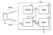
図5は、上述した半導体レーザ1を備えた照明装置100を用いた測距装置(測距装置200)の概略構成を表したブロック図である。測距装置200は、ToF方式により距離を測定するものである。測距装置200は、例えば、照明装置100と、受光部210と、制御部220と、測距部230とを有する。
Figure 5 is a block diagram showing the schematic configuration of a distance measuring device (distance measuring device 200) using the
照明装置100は、例えば、図1等に示した半導体レーザ1を光源として備えたものである。照明装置100では、例えば、矩形波の発光制御信号CLKpに同期して照明光を発生する。また、発光制御信号CLKpは、周期信号であれば、矩形波に限定されない。例えば、発光制御信号CLKpは、サイン波であってもよい。The
受光部210は、照射対象物300から反射された反射光を受光して、垂直同期信号VSYNCの周期が経過するたびに、その周期内の受光量を検出するものである。例えば、60ヘルツ(Hz)の周期信号が垂直同期信号VSYNCとして用いられる。また、受光部210には、複数の画素回路が二次元格子状に配置されている。受光部210は、これらの画素回路の受光量に応じた画像データ(フレーム)を測距部230に供給する。なお、垂直同期信号VSYNCの周波数は、60ヘルツ(Hz)に限定されず、30ヘルツ(Hz)や120ヘルツ(Hz)としてもよい。The
制御部220は、照明装置100を制御するものである。制御部220は、発光制御信号CLKpを生成して照明装置100および受光部210に供給する。発光制御信号CLKpの周波数は、例えば20メガヘルツ(MHz)である。なお、発光制御信号CLKpの周波数は、20メガヘルツ(MHz)に限定されず、例えば5メガヘルツ(MHz)としてもよい。The
測距部230は、画像データに基づいて、照射対象物300までの距離をToF方式で測定するものである。この測距部230は、画素回路毎に距離を測定して画素毎に物体までの距離を諧調値で示すデプスマップを生成する。このデプスマップは、例えば、距離に応じた度合いのぼかし処理を行う画像処理や、距離に応じてフォーカスレンズの合焦点を求めるオートフォーカス(AF)処理等に用いられる。The
以上、第1、第2の実施の形態および適用例を挙げて本技術を説明したが、本技術は上記実施の形態等に限定されるものではなく、種々変形が可能である。例えば、上記第1の実施の形態等において説明した半導体レーザ1,2の層構成は一例であり、更に他の層を備えていてもよい。また、各層の材料も一例であって、上述のものに限定されるものではない。
Although the present technology has been described above with reference to the first and second embodiments and application examples, the present technology is not limited to the above-mentioned embodiments, and various modifications are possible. For example, the layer configuration of the
例えば、上記第1の実施の形態等では、第1コンタクト層12が不純物(ドーパント)として炭素(C)を含む例を示したが、第1コンタクト層12のドーパントは炭素(C)に限らない。例えば、第1コンタクト層12は、バッファ層13と同様に、ドーパントとして亜鉛(Zn)等を含んでいてもよい。その場合には、第1コンタクト層12と接するバッファ層13の第1層13Aは省略しても構わない。For example, in the above first embodiment, an example has been shown in which the
また、上記第1の実施の形態では、基板11上に第1コンタクト層12、バッファ層13、第1光反射層14、活性層15、第2光反射層16および第2コンタクト層18がこの順に積層された、アノード共通構造を有する裏面出射型の半導体レーザ(半導体レーザ1)を例に示したがこれに限らない。例えば、半導体レーザ1は、第2の実施の形態の半導体レーザ2のように、基板11側から第2コンタクト層18、第2光反射層16、活性層15、第1光反射層14、バッファ層13および第1コンタクト層12がこの順に積層された、所謂カソード共通構造を有する裏面出射型の半導体レーザとして構成してもよい。同様に、上記第2の実施の形態において説明した表面出射型の半導体レーザ(半導体レーザ2)についても、基板11側から順に、第1コンタクト層12、バッファ層13、第1光反射層14、活性層15、第2光反射層16および第2コンタクト層18が積層された構成としてもよい。
In the first embodiment, a back-emitting semiconductor laser (semiconductor laser 1) having an anode common structure in which the
なお、本明細書に記載された効果はあくまで例示であって限定されるものではなく、また他の効果があってよい。 Note that the effects described in this specification are merely examples and are not limiting, and other effects may also exist.
なお、本技術は以下のような構成とすることができる。以下の構成の本技術によれば、半導体積層体を構成する、不純物として炭素を含むヒ素系半導体層からなる第1の光反射層と、リン系半導体層からなる第1のバッファ層との間に、不純物として亜鉛またはマグネシウムを含むヒ素系半導体層からなる第2のバッファ層を設けるようにした。これにより、第1の光反射層に不純物として含まれる炭素の原料とリン系半導体との接触による結晶成長面の表面状態の悪化が抑制され、デバイス特性の安定性および製造歩留まりを向上させることが可能となる。
(1)
基板と、
前記基板側から第2の光反射層、活性層および不純物として炭素を含むヒ素系半導体層からなる第1の光反射層の順に積層された半導体積層体と、
前記半導体積層体の前記第1の光反射層側に設けられ、前記半導体積層体に面する一の面および前記一の面とは反対側の他の面を有するリン系半導体層からなる第1のバッファ層と、
少なくとも前記第1の光反射層と前記第1のバッファ層との間に設けられ、不純物としてマグネシウムを含むヒ素系半導体層からなる第2のバッファ層と、
前記第1のバッファ層の前記他の面側に設けられると共に、不純物として炭素を含むヒ素系半導体層からなる第1のコンタクト層と、
前記基板と前記第2の光反射層との間に設けられた第2のコンタクト層とを備え、
前記第2のバッファ層は、前記第1のバッファ層の前記一の面および前記他の面の両方に設けられ、
前記第1のコンタクト層および前記第1のバッファ層の前記他の面側に設けられた前記第2のバッファ層に光出射面となる開口が形成されている
発光デバイス。
(2)
前記ヒ素系半導体層はGaAs層、AlGaAs層およびAlAs層のうちのいずれか1層または2層以上からなる単層膜または積層膜である、前記(1)に記載の発光デバイス。
(3)
前記リン系半導体層は、GaInP層、AlGaInP層およびAlInP層のうちのいずれか1層または2層以上からなる単層膜または積層膜である、前記(1)または(2)に記載の発光デバイス。
(4)
前記半導体積層体は、前記第1の光反射層と前記活性層との間に電流注入領域を有する電流狭窄層をさらに有する、前記(1)乃至(3)のうちのいずれか1つに記載の発光デバイス。
(5)
前記半導体積層体に対して所定の電圧を印加可能に設けられた第1の電極および第2の電極をさらに有する、前記(1)乃至(4)のうちのいずれか1つに記載の発光デバイス。
(6)
前記半導体積層体は、前記半導体積層体の上方にレーザ光を出射する、前記(1)乃至(5)のうちのいずれか1つに記載の発光デバイス。
(7)
基板上に第2のコンタクト層、第2の光反射層、活性層、不純物として炭素を含むヒ素系半導体層からなる第1の光反射層、不純物として亜鉛またはマグネシウムを含むヒ素系半導体層からなる第2のバッファ層、リン系半導体層からなる第1のバッファ層、前記第2のバッファ層および不純物として炭素を含むヒ素系半導体層からなる第1のコンタクト層を結晶成長によりこの順に形成した後、
前記第1のバッファ層をエッチングストップ層として前記第1のコンタクト層および前記第2のバッファ層をエッチングして、底面が光出射面となる開口を形成する
発光デバイスの製造方法。
(8)
前記第1のバッファ層、前記第2のバッファ層、前記第1の光反射層、前記活性層および前記第2の光反射層を有機金属気相成長法により連続して形成する、前記(7)に記載の発光デバイスの製造方法。
The present technology can be configured as follows. According to the present technology configured as follows, a second buffer layer made of an arsenic-based semiconductor layer containing zinc or magnesium as an impurity is provided between a first light reflecting layer made of an arsenic-based semiconductor layer containing carbon as an impurity and a first buffer layer made of a phosphorus-based semiconductor layer, which constitute a semiconductor laminate. This suppresses deterioration of the surface condition of the crystal growth surface due to contact between the carbon raw material contained as an impurity in the first light reflecting layer and the phosphorus-based semiconductor, making it possible to improve the stability of device characteristics and manufacturing yield.
(1)
A substrate;
a semiconductor laminate including a second light reflecting layer , an active layer, and a first light reflecting layer including an arsenic-based semiconductor layer containing carbon as an impurity, laminated in this order from the substrate side;
a first buffer layer formed on the first light reflecting layer side of the semiconductor laminate and made of a phosphorus-based semiconductor layer having one surface facing the semiconductor laminate and another surface opposite to the one surface;
a second buffer layer provided at least between the first light reflecting layer and the first buffer layer and made of an arsenic-based semiconductor layer containing magnesium as an impurity;
a first contact layer provided on the other surface side of the first buffer layer and made of an arsenic-based semiconductor layer containing carbon as an impurity;
a second contact layer provided between the substrate and the second light reflecting layer;
the second buffer layer is provided on both the one surface and the other surface of the first buffer layer;
An opening serving as a light emitting surface is formed in the first contact layer and the second buffer layer provided on the other surface side of the first buffer layer.
Light emitting device.
(2)
The light-emitting device according to (1) above, wherein the arsenic-based semiconductor layer is a single layer or a multilayer film made of one or more layers selected from the group consisting of a GaAs layer, an AlGaAs layer, and an AlAs layer.
(3)
The light-emitting device according to (1) or (2), wherein the phosphorus-based semiconductor layer is a single layer or a laminated film made of one or more layers selected from the group consisting of a GaInP layer, an AlGaInP layer, and an AlInP layer.
(4 )
The light-emitting device according to any one of (1) to (3), wherein the semiconductor laminate further includes a current confinement layer having a current injection region between the first light-reflecting layer and the active layer.
(5)
The light-emitting device according to any one of (1) to (4), further comprising a first electrode and a second electrode that are provided so as to be able to apply a predetermined voltage to the semiconductor laminate.
(6)
The light-emitting device according to any one of (1) to (5) , wherein the semiconductor stack emits laser light above the semiconductor stack.
(7)
a second contact layer, a second light reflecting layer, an active layer, a first light reflecting layer made of an arsenic-based semiconductor layer containing carbon as an impurity, a second buffer layer made of an arsenic-based semiconductor layer containing zinc or magnesium as an impurity , a first buffer layer made of a phosphorus-based semiconductor layer , the second buffer layer, and a first contact layer made of an arsenic-based semiconductor layer containing carbon as an impurity are formed in this order on a substrate by crystal growth;
the first contact layer and the second buffer layer are etched using the first buffer layer as an etching stop layer to form an opening whose bottom surface serves as a light emitting surface.
(8)
The method for manufacturing a light-emitting device according to (7), wherein the first buffer layer, the second buffer layer, the first light-reflecting layer, the active layer and the second light-reflecting layer are successively formed by metal-organic chemical vapor deposition.
本出願は、日本国特許庁において2020年2月18日に出願された日本特許出願番号2020-025190号を基礎として優先権を主張するものであり、この出願の全ての内容を参照によって本出願に援用する。This application claims priority based on Japanese Patent Application No. 2020-025190, filed on February 18, 2020, in the Japan Patent Office, the entire contents of which are incorporated herein by reference.
当業者であれば、設計上の要件や他の要因に応じて、種々の修正、コンビネーション、サブコンビネーション、および変更を想到し得るが、それらは添付の請求の範囲やその均等物の範囲に含まれるものであることが理解される。 Those skilled in the art will recognize that various modifications, combinations, subcombinations, and variations may occur to those skilled in the art depending on design requirements and other factors, and that these are intended to be within the scope of the appended claims and their equivalents.
Claims (8)
前記基板側から第2の光反射層、活性層および不純物として炭素を含むヒ素系半導体層からなる第1の光反射層の順に積層された半導体積層体と、
前記半導体積層体の前記第1の光反射層側に設けられ、前記半導体積層体に面する一の面および前記一の面とは反対側の他の面を有するリン系半導体層からなる第1のバッファ層と、
少なくとも前記第1の光反射層と前記第1のバッファ層との間に設けられ、不純物としてマグネシウムを含むヒ素系半導体層からなる第2のバッファ層と、
前記第1のバッファ層の前記他の面側に設けられると共に、不純物として炭素を含むヒ素系半導体層からなる第1のコンタクト層と、
前記基板と前記第2の光反射層との間に設けられた第2のコンタクト層とを備え、
前記第2のバッファ層は、前記第1のバッファ層の前記一の面および前記他の面の両方に設けられ、
前記第1のコンタクト層および前記第1のバッファ層の前記他の面側に設けられた前記第2のバッファ層に光出射面となる開口が形成されている
発光デバイス。 A substrate;
a semiconductor laminate including a second light reflecting layer , an active layer, and a first light reflecting layer including an arsenic-based semiconductor layer containing carbon as an impurity, laminated in this order from the substrate side;
a first buffer layer formed on the first light reflecting layer side of the semiconductor laminate and made of a phosphorus-based semiconductor layer having one surface facing the semiconductor laminate and another surface opposite to the one surface;
a second buffer layer provided at least between the first light reflecting layer and the first buffer layer and made of an arsenic-based semiconductor layer containing magnesium as an impurity;
a first contact layer provided on the other surface side of the first buffer layer and made of an arsenic-based semiconductor layer containing carbon as an impurity;
a second contact layer provided between the substrate and the second light reflecting layer;
the second buffer layer is provided on both the one surface and the other surface of the first buffer layer;
An opening serving as a light emitting surface is formed in the first contact layer and the second buffer layer provided on the other surface side of the first buffer layer.
Light emitting device.
前記第1のバッファ層をエッチングストップ層として前記第1のコンタクト層および前記第2のバッファ層をエッチングして、底面が光出射面となる開口を形成する
発光デバイスの製造方法。 a second contact layer, a second light reflecting layer, an active layer, a first light reflecting layer made of an arsenic-based semiconductor layer containing carbon as an impurity, a second buffer layer made of an arsenic-based semiconductor layer containing zinc or magnesium as an impurity , a first buffer layer made of a phosphorus-based semiconductor layer , the second buffer layer, and a first contact layer made of an arsenic-based semiconductor layer containing carbon as an impurity are formed in this order on a substrate by crystal growth;
the first contact layer and the second buffer layer are etched using the first buffer layer as an etching stop layer to form an opening whose bottom surface serves as a light emitting surface.
Applications Claiming Priority (3)
| Application Number | Priority Date | Filing Date | Title |
|---|---|---|---|
| JP2020025190 | 2020-02-18 | ||
| JP2020025190 | 2020-02-18 | ||
| PCT/JP2021/004102 WO2021166661A1 (en) | 2020-02-18 | 2021-02-04 | Light-emitting device and method for manufacturing light-emitting device |
Publications (2)
| Publication Number | Publication Date |
|---|---|
| JPWO2021166661A1 JPWO2021166661A1 (en) | 2021-08-26 |
| JP7660552B2 true JP7660552B2 (en) | 2025-04-11 |
Family
ID=77392067
Family Applications (1)
| Application Number | Title | Priority Date | Filing Date |
|---|---|---|---|
| JP2022501777A Active JP7660552B2 (en) | 2020-02-18 | 2021-02-04 | Light emitting device and method for manufacturing the same |
Country Status (5)
| Country | Link |
|---|---|
| US (1) | US20230090469A1 (en) |
| JP (1) | JP7660552B2 (en) |
| DE (1) | DE112021001065T5 (en) |
| TW (1) | TWI890733B (en) |
| WO (1) | WO2021166661A1 (en) |
Families Citing this family (2)
| Publication number | Priority date | Publication date | Assignee | Title |
|---|---|---|---|---|
| CN115313150B (en) * | 2022-08-02 | 2025-05-30 | 深圳市嘉敏利光电有限公司 | Vertical cavity surface emitting laser and preparation method thereof |
| EP4716038A1 (en) * | 2023-05-19 | 2026-03-25 | Sony Semiconductor Solutions Corporation | Surface light-emitting element |
Citations (9)
| Publication number | Priority date | Publication date | Assignee | Title |
|---|---|---|---|---|
| JP2000164982A (en) | 1998-11-30 | 2000-06-16 | Nippon Telegr & Teleph Corp <Ntt> | Surface emitting laser |
| JP2001223433A (en) | 1999-11-30 | 2001-08-17 | Ricoh Co Ltd | Vertical cavity semiconductor surface emitting laser device and optical system using the laser device |
| JP2003218467A (en) | 2002-01-28 | 2003-07-31 | Ricoh Co Ltd | Semiconductor distributed Bragg reflector, method of manufacturing the same, surface emitting semiconductor laser, optical communication module, and optical communication system |
| JP2004079833A (en) | 2002-08-20 | 2004-03-11 | Toshiba Corp | Vertical cavity surface emitting semiconductor laser |
| JP2007194561A (en) | 2006-01-23 | 2007-08-02 | Nec Corp | Surface emitting laser |
| JP2008258277A (en) | 2007-04-02 | 2008-10-23 | Sharp Corp | Semiconductor laser device, light emitting module, optical transmission module, and electronic device |
| JP2009054791A (en) | 2007-08-27 | 2009-03-12 | Hitachi Cable Ltd | Epitaxial wafer for light emitting device, method for manufacturing the same, and light emitting device |
| JP2013527484A (en) | 2009-12-19 | 2013-06-27 | トリルミナ コーポレーション | System and method for combining laser arrays for digital output |
| JP2015041627A (en) | 2013-08-20 | 2015-03-02 | ウシオ電機株式会社 | Semiconductor laser device |
Family Cites Families (25)
| Publication number | Priority date | Publication date | Assignee | Title |
|---|---|---|---|---|
| US4775980A (en) * | 1983-12-14 | 1988-10-04 | Hitachi, Ltd. | Distributed-feedback semiconductor laser device |
| JP2774582B2 (en) * | 1989-06-30 | 1998-07-09 | 株式会社東芝 | (III) —Method of manufacturing Group V compound semiconductor device |
| JPH03171789A (en) * | 1989-11-30 | 1991-07-25 | Toshiba Corp | Semiconductor laser device |
| JP3133187B2 (en) * | 1992-03-04 | 2001-02-05 | 富士通株式会社 | Semiconductor device and method of manufacturing the same |
| US5513202A (en) * | 1994-02-25 | 1996-04-30 | Matsushita Electric Industrial Co., Ltd. | Vertical-cavity surface-emitting semiconductor laser |
| US5892784A (en) * | 1994-10-27 | 1999-04-06 | Hewlett-Packard Company | N-drive p-common surface emitting laser fabricated on n+ substrate |
| US5625202A (en) * | 1995-06-08 | 1997-04-29 | University Of Central Florida | Modified wurtzite structure oxide compounds as substrates for III-V nitride compound semiconductor epitaxial thin film growth |
| US5724376A (en) * | 1995-11-30 | 1998-03-03 | Hewlett-Packard Company | Transparent substrate vertical cavity surface emitting lasers fabricated by semiconductor wafer bonding |
| JP3897186B2 (en) * | 1997-03-27 | 2007-03-22 | シャープ株式会社 | Compound semiconductor laser |
| JP3684778B2 (en) * | 1997-08-21 | 2005-08-17 | 富士ゼロックス株式会社 | Surface emitting semiconductor laser array |
| US6339496B1 (en) * | 1999-06-22 | 2002-01-15 | University Of Maryland | Cavity-less vertical semiconductor optical amplifier |
| US6692979B2 (en) * | 2001-08-13 | 2004-02-17 | Optoic Technology, Inc. | Methods of fabricating optoelectronic IC modules |
| DE10144826B4 (en) * | 2001-09-12 | 2007-03-08 | Forschungsverbund Berlin E.V. | Process for the production of surface emitting semiconductor devices and surface emitting semiconductor device |
| US7368759B2 (en) * | 2005-09-30 | 2008-05-06 | Hitachi Cable, Ltd. | Semiconductor light-emitting device |
| JP4548329B2 (en) * | 2005-12-19 | 2010-09-22 | セイコーエプソン株式会社 | Surface emitting semiconductor laser |
| JP5310371B2 (en) * | 2009-08-10 | 2013-10-09 | ソニー株式会社 | Semiconductor light emitting device and manufacturing method thereof |
| JP5765892B2 (en) * | 2010-05-27 | 2015-08-19 | キヤノン株式会社 | Vertical cavity surface emitting laser and image forming apparatus using the same |
| TW201401699A (en) * | 2012-04-09 | 2014-01-01 | Sony Corp | Semiconductor laser device assembly |
| KR20160078348A (en) * | 2013-10-29 | 2016-07-04 | 휴렛 팩커드 엔터프라이즈 디벨롭먼트 엘피 | High contrast grating optoelectronics |
| WO2017145026A1 (en) * | 2016-02-23 | 2017-08-31 | Silanna UV Technologies Pte Ltd | Resonant optical cavity light emitting device |
| JP2019012721A (en) * | 2017-06-29 | 2019-01-24 | セイコーエプソン株式会社 | Surface emitting laser and method for manufacturing the same, electronic device, and printer |
| WO2019107273A1 (en) * | 2017-11-30 | 2019-06-06 | ソニーセミコンダクタソリューションズ株式会社 | Surface emission semiconductor laser |
| JP7037061B2 (en) | 2018-08-07 | 2022-03-16 | 日本電信電話株式会社 | Communication system, optical transmitter and receiver |
| JP7247615B2 (en) * | 2019-01-31 | 2023-03-29 | 株式会社リコー | Surface emitting laser module, optical device and surface emitting laser substrate |
| CN110739604B (en) * | 2019-10-24 | 2021-03-09 | 厦门乾照半导体科技有限公司 | Semiconductor epitaxial structure based on flexible substrate, VCSEL and manufacturing method |
-
2021
- 2021-01-28 TW TW110103202A patent/TWI890733B/en active
- 2021-02-04 JP JP2022501777A patent/JP7660552B2/en active Active
- 2021-02-04 WO PCT/JP2021/004102 patent/WO2021166661A1/en not_active Ceased
- 2021-02-04 DE DE112021001065.4T patent/DE112021001065T5/en active Pending
- 2021-02-04 US US17/904,073 patent/US20230090469A1/en active Pending
Patent Citations (9)
| Publication number | Priority date | Publication date | Assignee | Title |
|---|---|---|---|---|
| JP2000164982A (en) | 1998-11-30 | 2000-06-16 | Nippon Telegr & Teleph Corp <Ntt> | Surface emitting laser |
| JP2001223433A (en) | 1999-11-30 | 2001-08-17 | Ricoh Co Ltd | Vertical cavity semiconductor surface emitting laser device and optical system using the laser device |
| JP2003218467A (en) | 2002-01-28 | 2003-07-31 | Ricoh Co Ltd | Semiconductor distributed Bragg reflector, method of manufacturing the same, surface emitting semiconductor laser, optical communication module, and optical communication system |
| JP2004079833A (en) | 2002-08-20 | 2004-03-11 | Toshiba Corp | Vertical cavity surface emitting semiconductor laser |
| JP2007194561A (en) | 2006-01-23 | 2007-08-02 | Nec Corp | Surface emitting laser |
| JP2008258277A (en) | 2007-04-02 | 2008-10-23 | Sharp Corp | Semiconductor laser device, light emitting module, optical transmission module, and electronic device |
| JP2009054791A (en) | 2007-08-27 | 2009-03-12 | Hitachi Cable Ltd | Epitaxial wafer for light emitting device, method for manufacturing the same, and light emitting device |
| JP2013527484A (en) | 2009-12-19 | 2013-06-27 | トリルミナ コーポレーション | System and method for combining laser arrays for digital output |
| JP2015041627A (en) | 2013-08-20 | 2015-03-02 | ウシオ電機株式会社 | Semiconductor laser device |
Also Published As
| Publication number | Publication date |
|---|---|
| WO2021166661A1 (en) | 2021-08-26 |
| DE112021001065T5 (en) | 2022-12-08 |
| TWI890733B (en) | 2025-07-21 |
| US20230090469A1 (en) | 2023-03-23 |
| JPWO2021166661A1 (en) | 2021-08-26 |
| TW202135340A (en) | 2021-09-16 |
Similar Documents
| Publication | Publication Date | Title |
|---|---|---|
| US11942762B2 (en) | Surface-emitting laser device and light emitting device including the same | |
| US12068577B2 (en) | Surface emitting laser, surface emitting laser device, light source device, and detection apparatus | |
| US12506325B2 (en) | Light emitting device and method of manufacturing light emitting device | |
| JP7795900B2 (en) | Vertical cavity light emitting device | |
| US12046872B2 (en) | Surface emitting laser, surface emitting laser device, light source device, and detection apparatus | |
| JP7660552B2 (en) | Light emitting device and method for manufacturing the same | |
| CN115298917A (en) | Light-emitting element, light-emitting element unit, electronic device, light-emitting device, sensing device, and communication device | |
| US12407146B2 (en) | Vertical cavity light-emitting element and manufacturing method of the same | |
| JP7685986B2 (en) | Surface-emitting laser | |
| TWI887340B (en) | Light emitting device | |
| JP7556888B2 (en) | Light emitting device and method for manufacturing the same | |
| US20230112925A1 (en) | Surface emitting laser | |
| JP2009059733A (en) | Surface emitting laser, and its manufacturing method | |
| JP7622039B2 (en) | Surface-emitting laser | |
| JP2009059734A (en) | Surface emitting laser | |
| JP7413901B2 (en) | light emitting element | |
| WO2024190073A1 (en) | Surface-emitting laser and surface-emitting laser array | |
| TW202504193A (en) | Surface Emitting Laser | |
| WO2023243298A1 (en) | Vertical cavity surface-emitting laser element, and array of vertical cavity surface-emitting laser elements | |
| JP2003324249A (en) | Surface emitting semiconductor laser and method of manufacturing the same |
Legal Events
| Date | Code | Title | Description |
|---|---|---|---|
| A621 | Written request for application examination |
Free format text: JAPANESE INTERMEDIATE CODE: A621 Effective date: 20240118 |
|
| A131 | Notification of reasons for refusal |
Free format text: JAPANESE INTERMEDIATE CODE: A131 Effective date: 20241001 |
|
| A521 | Request for written amendment filed |
Free format text: JAPANESE INTERMEDIATE CODE: A523 Effective date: 20241119 |
|
| A131 | Notification of reasons for refusal |
Free format text: JAPANESE INTERMEDIATE CODE: A131 Effective date: 20241203 |
|
| A521 | Request for written amendment filed |
Free format text: JAPANESE INTERMEDIATE CODE: A523 Effective date: 20250127 |
|
| TRDD | Decision of grant or rejection written | ||
| A01 | Written decision to grant a patent or to grant a registration (utility model) |
Free format text: JAPANESE INTERMEDIATE CODE: A01 Effective date: 20250304 |
|
| A61 | First payment of annual fees (during grant procedure) |
Free format text: JAPANESE INTERMEDIATE CODE: A61 Effective date: 20250401 |
|
| R150 | Certificate of patent or registration of utility model |
Ref document number: 7660552 Country of ref document: JP Free format text: JAPANESE INTERMEDIATE CODE: R150 |