JP4548329B2 - Surface emitting semiconductor laser - Google Patents
Surface emitting semiconductor laser Download PDFInfo
- Publication number
- JP4548329B2 JP4548329B2 JP2005364754A JP2005364754A JP4548329B2 JP 4548329 B2 JP4548329 B2 JP 4548329B2 JP 2005364754 A JP2005364754 A JP 2005364754A JP 2005364754 A JP2005364754 A JP 2005364754A JP 4548329 B2 JP4548329 B2 JP 4548329B2
- Authority
- JP
- Japan
- Prior art keywords
- refractive index
- mirror
- layer
- semiconductor laser
- region
- Prior art date
- Legal status (The legal status is an assumption and is not a legal conclusion. Google has not performed a legal analysis and makes no representation as to the accuracy of the status listed.)
- Expired - Fee Related
Links
Images


Classifications
-
- H—ELECTRICITY
- H01—ELECTRIC ELEMENTS
- H01S—DEVICES USING THE PROCESS OF LIGHT AMPLIFICATION BY STIMULATED EMISSION OF RADIATION [LASER] TO AMPLIFY OR GENERATE LIGHT; DEVICES USING STIMULATED EMISSION OF ELECTROMAGNETIC RADIATION IN WAVE RANGES OTHER THAN OPTICAL
- H01S5/00—Semiconductor lasers
- H01S5/10—Construction or shape of the optical resonator, e.g. extended or external cavity, coupled cavities, bent-guide, varying width, thickness or composition of the active region
- H01S5/18—Surface-emitting [SE] lasers, e.g. having both horizontal and vertical cavities
- H01S5/183—Surface-emitting [SE] lasers, e.g. having both horizontal and vertical cavities having only vertical cavities, e.g. vertical cavity surface-emitting lasers [VCSEL]
- H01S5/18308—Surface-emitting [SE] lasers, e.g. having both horizontal and vertical cavities having only vertical cavities, e.g. vertical cavity surface-emitting lasers [VCSEL] having a special structure for lateral current or light confinement
- H01S5/18322—Position of the structure
- H01S5/18327—Structure being part of a DBR
-
- B—PERFORMING OPERATIONS; TRANSPORTING
- B82—NANOTECHNOLOGY
- B82Y—SPECIFIC USES OR APPLICATIONS OF NANOSTRUCTURES; MEASUREMENT OR ANALYSIS OF NANOSTRUCTURES; MANUFACTURE OR TREATMENT OF NANOSTRUCTURES
- B82Y20/00—Nanooptics, e.g. quantum optics or photonic crystals
-
- H—ELECTRICITY
- H01—ELECTRIC ELEMENTS
- H01S—DEVICES USING THE PROCESS OF LIGHT AMPLIFICATION BY STIMULATED EMISSION OF RADIATION [LASER] TO AMPLIFY OR GENERATE LIGHT; DEVICES USING STIMULATED EMISSION OF ELECTROMAGNETIC RADIATION IN WAVE RANGES OTHER THAN OPTICAL
- H01S5/00—Semiconductor lasers
- H01S5/02—Structural details or components not essential to laser action
- H01S5/024—Arrangements for thermal management
-
- H—ELECTRICITY
- H01—ELECTRIC ELEMENTS
- H01S—DEVICES USING THE PROCESS OF LIGHT AMPLIFICATION BY STIMULATED EMISSION OF RADIATION [LASER] TO AMPLIFY OR GENERATE LIGHT; DEVICES USING STIMULATED EMISSION OF ELECTROMAGNETIC RADIATION IN WAVE RANGES OTHER THAN OPTICAL
- H01S5/00—Semiconductor lasers
- H01S5/10—Construction or shape of the optical resonator, e.g. extended or external cavity, coupled cavities, bent-guide, varying width, thickness or composition of the active region
- H01S5/18—Surface-emitting [SE] lasers, e.g. having both horizontal and vertical cavities
- H01S5/183—Surface-emitting [SE] lasers, e.g. having both horizontal and vertical cavities having only vertical cavities, e.g. vertical cavity surface-emitting lasers [VCSEL]
- H01S5/18308—Surface-emitting [SE] lasers, e.g. having both horizontal and vertical cavities having only vertical cavities, e.g. vertical cavity surface-emitting lasers [VCSEL] having a special structure for lateral current or light confinement
- H01S5/18311—Surface-emitting [SE] lasers, e.g. having both horizontal and vertical cavities having only vertical cavities, e.g. vertical cavity surface-emitting lasers [VCSEL] having a special structure for lateral current or light confinement using selective oxidation
-
- H—ELECTRICITY
- H01—ELECTRIC ELEMENTS
- H01S—DEVICES USING THE PROCESS OF LIGHT AMPLIFICATION BY STIMULATED EMISSION OF RADIATION [LASER] TO AMPLIFY OR GENERATE LIGHT; DEVICES USING STIMULATED EMISSION OF ELECTROMAGNETIC RADIATION IN WAVE RANGES OTHER THAN OPTICAL
- H01S5/00—Semiconductor lasers
- H01S5/10—Construction or shape of the optical resonator, e.g. extended or external cavity, coupled cavities, bent-guide, varying width, thickness or composition of the active region
- H01S5/18—Surface-emitting [SE] lasers, e.g. having both horizontal and vertical cavities
- H01S5/183—Surface-emitting [SE] lasers, e.g. having both horizontal and vertical cavities having only vertical cavities, e.g. vertical cavity surface-emitting lasers [VCSEL]
- H01S5/18361—Structure of the reflectors, e.g. hybrid mirrors
- H01S5/18369—Structure of the reflectors, e.g. hybrid mirrors based on dielectric materials
-
- H—ELECTRICITY
- H01—ELECTRIC ELEMENTS
- H01S—DEVICES USING THE PROCESS OF LIGHT AMPLIFICATION BY STIMULATED EMISSION OF RADIATION [LASER] TO AMPLIFY OR GENERATE LIGHT; DEVICES USING STIMULATED EMISSION OF ELECTROMAGNETIC RADIATION IN WAVE RANGES OTHER THAN OPTICAL
- H01S5/00—Semiconductor lasers
- H01S5/20—Structure or shape of the semiconductor body to guide the optical wave ; Confining structures perpendicular to the optical axis, e.g. index or gain guiding, stripe geometry, broad area lasers, gain tailoring, transverse or lateral reflectors, special cladding structures, MQW barrier reflection layers
- H01S5/204—Strongly index guided structures
-
- H—ELECTRICITY
- H01—ELECTRIC ELEMENTS
- H01S—DEVICES USING THE PROCESS OF LIGHT AMPLIFICATION BY STIMULATED EMISSION OF RADIATION [LASER] TO AMPLIFY OR GENERATE LIGHT; DEVICES USING STIMULATED EMISSION OF ELECTROMAGNETIC RADIATION IN WAVE RANGES OTHER THAN OPTICAL
- H01S5/00—Semiconductor lasers
- H01S5/30—Structure or shape of the active region; Materials used for the active region
- H01S5/34—Structure or shape of the active region; Materials used for the active region comprising quantum well or superlattice structures, e.g. single quantum well [SQW] lasers, multiple quantum well [MQW] lasers or graded index separate confinement heterostructure [GRINSCH] lasers
- H01S5/343—Structure or shape of the active region; Materials used for the active region comprising quantum well or superlattice structures, e.g. single quantum well [SQW] lasers, multiple quantum well [MQW] lasers or graded index separate confinement heterostructure [GRINSCH] lasers in AIIIBV compounds, e.g. AlGaAs-laser, InP-based laser
- H01S5/34313—Structure or shape of the active region; Materials used for the active region comprising quantum well or superlattice structures, e.g. single quantum well [SQW] lasers, multiple quantum well [MQW] lasers or graded index separate confinement heterostructure [GRINSCH] lasers in AIIIBV compounds, e.g. AlGaAs-laser, InP-based laser with a well layer having only As as V-compound, e.g. AlGaAs, InGaAs
- H01S5/3432—Structure or shape of the active region; Materials used for the active region comprising quantum well or superlattice structures, e.g. single quantum well [SQW] lasers, multiple quantum well [MQW] lasers or graded index separate confinement heterostructure [GRINSCH] lasers in AIIIBV compounds, e.g. AlGaAs-laser, InP-based laser with a well layer having only As as V-compound, e.g. AlGaAs, InGaAs the whole junction comprising only (AI)GaAs
-
- H—ELECTRICITY
- H01—ELECTRIC ELEMENTS
- H01S—DEVICES USING THE PROCESS OF LIGHT AMPLIFICATION BY STIMULATED EMISSION OF RADIATION [LASER] TO AMPLIFY OR GENERATE LIGHT; DEVICES USING STIMULATED EMISSION OF ELECTROMAGNETIC RADIATION IN WAVE RANGES OTHER THAN OPTICAL
- H01S2301/00—Functional characteristics
- H01S2301/16—Semiconductor lasers with special structural design to influence the modes, e.g. specific multimode
- H01S2301/166—Single transverse or lateral mode
-
- H—ELECTRICITY
- H01—ELECTRIC ELEMENTS
- H01S—DEVICES USING THE PROCESS OF LIGHT AMPLIFICATION BY STIMULATED EMISSION OF RADIATION [LASER] TO AMPLIFY OR GENERATE LIGHT; DEVICES USING STIMULATED EMISSION OF ELECTROMAGNETIC RADIATION IN WAVE RANGES OTHER THAN OPTICAL
- H01S2301/00—Functional characteristics
- H01S2301/17—Semiconductor lasers comprising special layers
- H01S2301/176—Specific passivation layers on surfaces other than the emission facet
-
- H—ELECTRICITY
- H01—ELECTRIC ELEMENTS
- H01S—DEVICES USING THE PROCESS OF LIGHT AMPLIFICATION BY STIMULATED EMISSION OF RADIATION [LASER] TO AMPLIFY OR GENERATE LIGHT; DEVICES USING STIMULATED EMISSION OF ELECTROMAGNETIC RADIATION IN WAVE RANGES OTHER THAN OPTICAL
- H01S5/00—Semiconductor lasers
- H01S5/10—Construction or shape of the optical resonator, e.g. extended or external cavity, coupled cavities, bent-guide, varying width, thickness or composition of the active region
- H01S5/18—Surface-emitting [SE] lasers, e.g. having both horizontal and vertical cavities
- H01S5/183—Surface-emitting [SE] lasers, e.g. having both horizontal and vertical cavities having only vertical cavities, e.g. vertical cavity surface-emitting lasers [VCSEL]
- H01S5/18305—Surface-emitting [SE] lasers, e.g. having both horizontal and vertical cavities having only vertical cavities, e.g. vertical cavity surface-emitting lasers [VCSEL] with emission through the substrate, i.e. bottom emission
Description
本発明は、面発光型半導体レーザ に関する。
The present invention relates to a surface emitting semiconductor laser. About.
近年、面発光型半導体レーザにおける情報量の拡大、及び用途の多様化等により発振モード数を削減しつつ高出力化することが望まれている。一般には、共振器体積を小さくすることにより、モード数を削減することができる。 In recent years, it has been desired to increase the output while reducing the number of oscillation modes by expanding the amount of information in a surface-emitting type semiconductor laser and diversifying applications. In general, the number of modes can be reduced by reducing the resonator volume.
一方、半導体レーザの出力は、注入される電流値とともに大きくなり、ある電流値において最大値(ロールオフ点)に達する。半導体レーザでは、電流注入によりデバイス温度が上昇するとともに、利得スペクトルがシフトし、ある温度で利得が最大値を迎えるためである。共振器体積が小さい場合、デバイス温度が上昇しやすく、低い電流値でロールオフ点に達するため十分な出力や電流駆動範囲が得られない場合がある。十分な出力が得られない場合、駆動点とロールオフが近づくため、駆動電流範囲を狭くしなければ、環境温度による出力のゆらぎが大きくなってしまう。そこで、デバイス温度の上昇を防止するために、特許文献1には、発光部の周辺部に電流狭窄部に達するまで溝を掘り、この溝上に直接電極を形成する方法が開示されている。これにより、発熱部から電極までの距離を短くして放熱性を高めている。
本発明の目的は、モード数を削減することができ、かつ高出力化の可能な面発光型半導体レーザおよびその製造方法を提供することにある。 An object of the present invention is to provide a surface-emitting type semiconductor laser capable of reducing the number of modes and increasing the output, and a method for manufacturing the same.
本発明にかかる面発光型半導体レーザは、
第1ミラーと、
前記第1ミラーの上方に形成された活性層と、
前記活性層の上方に形成された第2ミラーと、
前記活性層の上方または下方に形成された電流狭窄層と、
を含み、
前記第2ミラーは、低屈折率領域に周囲を囲まれた高屈折率領域を有し、
前記高屈折率領域は、平面視において前記電流狭窄層に囲まれた領域の内側に形成されている。
The surface emitting semiconductor laser according to the present invention is
A first mirror;
An active layer formed above the first mirror;
A second mirror formed above the active layer;
A current confinement layer formed above or below the active layer;
Including
The second mirror has a high refractive index region surrounded by a low refractive index region,
The high refractive index region is formed inside a region surrounded by the current confinement layer in plan view.
本発明にかかる面発光型半導体レーザにおいて、
前記第2ミラーは、多層膜ミラーであり、
前記高屈折率領域の上方に交互に積層された高屈折率層と低屈折率層とをさらに有することができる。
In the surface emitting semiconductor laser according to the present invention,
The second mirror is a multilayer mirror;
It may further include a high refractive index layer and a low refractive index layer alternately stacked above the high refractive index region.
本発明にかかる面発光型半導体レーザにおいて、
少なくとも前記活性層、前記第2ミラー、および前記電流狭窄層によって構成される第1の柱状部を含み、
前記第1の柱状部は、前記活性層と前記電流狭窄層とを有する第3の柱状部と、当該第3の柱状部の上方に形成された前記活性層より小さい径を有する第2の柱状部と、
前記第3の柱状部の上面かつ前記第2の柱状部の周囲に形成された電極をさらに含むことができる。
In the surface emitting semiconductor laser according to the present invention,
Including at least a first columnar portion constituted by the active layer, the second mirror, and the current confinement layer;
The first columnar section includes a third columnar section having the active layer and the current confinement layer, and a second columnar section having a smaller diameter than the active layer formed above the third columnar section. And
The electrode may further include an electrode formed on an upper surface of the third columnar portion and around the second columnar portion.
本発明にかかる面発光型半導体レーザにおいて、
前記第2ミラーを構成する高屈折率層および低屈折率層のうち、少なくとも一層は、誘電体層であることができる。
In the surface emitting semiconductor laser according to the present invention,
At least one of the high refractive index layer and the low refractive index layer constituting the second mirror may be a dielectric layer.
本発明にかかる面発光型半導体レーザにおいて、
前記高屈折率領域は、半導体層からなり、
前記低屈折率領域、高屈折率層、および低屈折率層は、誘電体層からなることができる。
In the surface emitting semiconductor laser according to the present invention,
The high refractive index region is composed of a semiconductor layer,
The low refractive index region, the high refractive index layer, and the low refractive index layer may be made of a dielectric layer.
本発明にかかる面発光型半導体レーザにおいて、
前記第2ミラーの上方に形成された放熱膜をさらに含むことができる。
In the surface emitting semiconductor laser according to the present invention,
The heat dissipation film may be further formed above the second mirror.
本発明にかかる面発光型半導体レーザにおいて、
前記放熱膜は、光透過性を有することができる。
In the surface emitting semiconductor laser according to the present invention,
The heat dissipation film may have light permeability.
本発明にかかる面発光型半導体レーザにおいて、
前記放熱膜は、導電性材料からなり、
前記第2ミラーと前記放熱膜との間に光透過性を有する絶縁膜をさらに含むことができる。
In the surface emitting semiconductor laser according to the present invention,
The heat dissipation film is made of a conductive material,
An insulating film having optical transparency may be further included between the second mirror and the heat dissipation film.
本発明にかかる面発光型半導体レーザの製造方法は、
(a)基板側から、第1ミラー、活性層、および高屈折率領域を構成するための半導体層を積層する工程と、
(b)前記高屈折率領域を構成するための半導体層を所定の形状にパターニングして、高屈折率領域を形成する工程と、
(c)前記第2ミラーを構成するための低屈折率層および高屈折率層を、前記高屈折率領域の上方に積層する工程と、
(d)前記第1ミラーまたは第2ミラーに電流狭窄層を形成する工程と、
を含み、
前記高屈折率領域は、平面視において前記電流狭窄層に囲まれた領域の内側に形成されている。
A method of manufacturing a surface emitting semiconductor laser according to the present invention includes:
(A) laminating a first mirror, an active layer, and a semiconductor layer for constituting a high refractive index region from the substrate side;
(B) patterning a semiconductor layer for forming the high refractive index region into a predetermined shape to form the high refractive index region;
(C) laminating a low refractive index layer and a high refractive index layer for constituting the second mirror above the high refractive index region;
(D) forming a current confinement layer on the first mirror or the second mirror;
Including
The high refractive index region is formed inside a region surrounded by the current confinement layer in plan view.
本発明にかかる面発光型半導体レーザの製造方法において、
前記工程(c)では、
前記第2ミラーを構成するための低屈折率層および高屈折率層として、誘電体層を積層することができる。
In the method of manufacturing the surface emitting semiconductor laser according to the present invention,
In the step (c),
A dielectric layer can be laminated as a low refractive index layer and a high refractive index layer for constituting the second mirror.
以下、本発明の好適な実施の形態について、図面を参照しながら説明する。 Hereinafter, preferred embodiments of the present invention will be described with reference to the drawings.
1.面発光型半導体レーザ
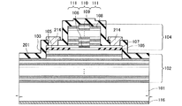
図1は、実施の形態にかかる面発光型半導体レーザ100を模式的に示す断面図である。図2は、実施の形態にかかる面発光型半導体レーザ100を模式的に示す平面図である。図1は、図2に示すC−C線に沿った断面を示す図である。
1. Surface Emitting Semiconductor Laser FIG. 1 is a cross-sectional view schematically showing a surface emitting
面発光型半導体レーザ100は、基板101と、第1ミラー102と、活性層103と、第2ミラー104とを含む。面発光型半導体レーザ100は、垂直共振器を有し、図1および図2に示すように、柱状の半導体堆積体(以下「第1の柱状部」とする)130を含むことができる。第1の柱状部130は、第1ミラー102の一部、活性層103および第2ミラー104によって構成される。
The surface emitting
基板101は、半導体基板からなることができ、たとえばn型GaAs基板からなることができる。第1ミラー102は、例えば、n型Al0.9Ga0.1As層とn型Al0.15Ga0.85As層とを交互に積層した40ペアの分布反射型多層膜ミラーからなることができる。活性層103は、GaAsウエル層とAl0.3Ga0.7Asバリア層からなり、ウエル層が3層で構成される量子井戸構造を含むことができる。
The
第2ミラー104は、活性層の近領域に形成された電流狭窄層105と、高屈折率領域106と、低屈折率領域107とを有する。第2ミラー104は、分布反射型多層膜ミラーとして機能することができる。
The
電流狭窄層105は、酸化狭窄層またはプロトン打ち込み領域により形成される。電流狭窄層105は、たとえばAlxGa1-xAs(x>0.95)層を側面から酸化することにより得られ、平面視においてリング形状を有することができる。
The
高屈折率領域106は、電流狭窄層105が設けられる層の上方に形成される。また高屈折率領域106は、低屈折率領域107に周囲を囲まれている。高屈折率領域106は、平面視において電流狭窄層105に囲まれた領域の内側(第1の領域110)に形成される。即ち、図1および図2に示すように、電流狭窄層105の内径Aは、高屈折率領域106の径Bより大きい。これにより、高屈折率領域106において光閉じこめが行われ、発振モード数は、高屈折率領域106の径Bによって決定される。一方、電流閉じこめは、電流狭窄層105において行われるため、電流狭窄層105の内径Aを大きくすることにより、大電流を注入した場合でも発熱量を抑制でき、ロールオフ点における電流量を大きくし、高出力化することができる。また、高出力化によりロールオフを迎える電流が駆動電流範囲から離れるため、広い温度範囲での動作を可能とすることができる。即ち、電流狭窄層105の内径Aを大きくし、同時に高屈折率領域106の径Bを小さくすることにより、発振モード数を低減するとともに、高出力化を可能とすることができる。
The high
また、図1に示すように、高屈折率領域106は、活性層103の近傍に形成されることが好ましい。これにより、効率的に光閉じこめを行うことができる。
Further, as shown in FIG. 1, the high
高屈折率領域106は、周囲に形成された低屈折率領域107より高い屈折率を有すればよい。すなわち高屈折率領域106および低屈折率領域107が、p型AlGaAs層からなる場合には、高屈折率領域106のAl組成が、低屈折率領域107より高い。たとえば、高屈折率領域106は、p型Al0.1Ga0.9As層からなることができ、低屈折率領域107は、p型Al0.85Ga0.15As層からなることができる。なお、高屈折率領域106の径Bは、所望のモード数、設計波長等に応じて適宜調整することができる。
The high refractive index area |
低屈折率領域107は、上述したように高屈折率領域106より低い屈折率を有すればよく、たとえばp型Al0.85Ga0.15As層からなることができる。
The low
さらに、第2ミラー104は、高屈折率領域106および低屈折率領域107の上方に交互に積層された高屈折率層108および低屈折率層109を有する。たとえば高屈折率層108は、p型Al0.9Ga0.1As層からなり、低屈折率層109は、p型Al0.15Ga0.85As層からなることができる。これにより、高屈折率層108および低屈折率層109は、ミラーとして機能することができる。なお、高屈折率層108および低屈折率層109は、電流狭窄層105が設けられている層と高屈折率領域106および低屈折率領域107との間に交互に形成されていてもよい。
Further, the
第1の柱状部130は、第2の柱状部140および第3の柱状部150を有する。第2の柱状部140は、電流狭窄層105が設けられている層の上方に形成され、高屈折率層108および低屈折率層109を有する。第3の柱状部150は、第1ミラー102の一部、活性層103、第2ミラー104の一部、および電流狭窄層105を有する。高屈折率領域106および低屈折率領域107については、第2の柱状部140および第3の柱状部150のいずれが有してもよい。本実施の形態においては、第3の柱状部150が高屈折率領域106および低屈折率領域107を有する。
The first
また第2の柱状部140は、第1の領域110および第2の領域111に形成される。図1および図2に示すように、第1の領域110は、平面視において円形状を有し、第2の領域111は、平面視においてリング形状を有し、第1の領域110の周囲に設けられている。なお、低屈折率領域107は、高屈折率領域106の周囲(第2の領域111)だけでなく、第1の領域110において高屈折率領域106の上面にも形成されていてもよい。この場合、第1の領域110および第2の領域111の双方の上面に、高屈折率層108が形成され、さらにその上面に低屈折率層109が形成される。
The second
第3の柱状部150の上面には、第1電極114が形成されるため、第3の柱状部150の最上層の導電性を向上することで、より均一に電流注入を行うことができる。したがって、第3の柱状部150の最上層の第1電極114が形成される領域には、Alを含まないGaAs層、もしくは高屈折率領域106のようなAlをほとんど含まないAlGaAs層が形成されていることが好ましい。
Since the
第2ミラー104は、たとえば炭素(C)がドーピングされることによりp型にされ、第1ミラー102は、たとえばケイ素(Si)がドーピングされることによりn型にされている。したがって、p型の第2ミラー104、不純物がドーピングされていない活性層103、およびn型の第1ミラー102により、pinダイオードが形成される。なお、本実施の形態において、第2の柱状部140および第3の柱状部150は、平面視において、円形状を有するとしたが、この形状は任意の形状をとることができる。
The
また、面発光型半導体レーザ100は、第1電極114および第2電極116をさらに含む。この第1電極114および第2電極116は、面発光型半導体レーザ100を駆動するために使用される。
The surface emitting
具体的には、図1に示すように、第1電極114は、第3の柱状部150の上面に形成される。第2電極116は、半導体基板101の裏面に形成される。第1電極114は、たとえば図2に示すようなリング状の平面形状を有することができる。すなわち、第1電極114は主として第2の柱状部140を取り囲むように任意の形状に設けられている。また第1電極114は、第3の柱状部150に接するリング形状部から引き出された直線形状の引き出し部を有してもよい。
Specifically, as shown in FIG. 1, the
なお、本実施の形態では、第2電極116は半導体基板101の裏面に設けられているが、第1ミラー102の上面に設けられていてもよい。
In the present embodiment, the
第2電極116は、例えば金(Au)とゲルマニウム(Ge)の合金と、金(Au)との積層膜からなる。また、第1電極114は、例えば白金(Pt)、チタン(Ti)および金(Au)の積層膜からなる。第1電極114と第2電極116とによって活性層103に電流が注入される。なお、第1電極114および第2電極116を形成するための材料は、前述したものに限定されるわけではなく、例えば金(Au)と亜鉛(Zn)との合金などが利用可能である。面発光型半導体レーザ100は、第1電極114の内側から上方に向かって、発振モード数の削減された光を出射することができる。
The
2.面発光型半導体レーザの製造方法
次に、本発明を適用した実施の形態に係る面発光型半導体レーザ100の製造方法の一例について、図3〜図8を用いて説明する。図3〜図8は、図1および図2に示す面発光型半導体レーザ100の一製造工程を模式的に示す断面図であり、それぞれ図1に示す断面図に対応している。
2. Method for Manufacturing Surface Emitting Semiconductor Laser Next, an example of a method for manufacturing the surface emitting
(1)まず、n型GaAs層からなる基板101の表面に、組成を変調させながらエピタキシャル成長させることにより、図3に示すように、半導体多層膜が形成される。ここで、半導体多層膜は、例えば、n型Al0.9Ga0.1As層とn型Al0.1Ga0.9As層とを交互に積層した38.5ペアの第1ミラー102a、GaAsウエル層とAl0.3Ga0.7Asバリア層からなり、ウエル層が3層で構成される量子井戸構造を含む活性層103a、p型AlAs層またはp型AlGaAs層からなる低屈折率層105a、p型Al0.1Ga0.9As層からなる高屈折率層106a、からなることができる。
(1) First, as shown in FIG. 3, a semiconductor multilayer film is formed on the surface of the
低屈折率層105aと活性層103aとの間、低屈折率層105aと高屈折率層106aとの間、および高屈折率層106aの上面には、さらにp型Al0.9Ga0.1As層とp型Al0.1Ga0.9As層とが交互に積層されていてもよい。
P-type Al 0.9 Ga 0.1 is further provided between the low
低屈折率層105aは、後に酸化されて電極狭窄層105となる。低屈折率層105aにおいて、Alの組成比は高いことが好ましく、例えば0.95以上であることが望ましい。
The low
エピタキシャル成長を行う際の温度は、成長方法や原料、基板101の種類、あるいは形成する半導体多層膜の種類、厚さ、およびキャリア密度によって適宜決定されるが、一般に、450℃〜800℃であるのが好ましい。また、エピタキシャル成長を行う際の所要時間も、温度と同様に適宜決定される。また、エピタキシャル成長させる方法としては、有機金属気相成長(MOVPE:Metal−Organic Vapor Phase Epitaxy)法や、MBE法(Molecular Beam Epitaxy)法、あるいはLPE法(Liquid Phase Epitaxy)を用いることができる。
The temperature at which the epitaxial growth is performed is appropriately determined depending on the growth method, the raw material, the type of the
(2)次に、公知のリソグラフィ技術およびエッチング技術を用いて、高屈折率層106aを所望の形状にパターニングする。このとき、図3に示すように、高屈折率領域106の形成領域110にレジスト層R1が設けられ、たとえばドライエッチングにより、高屈折率層106aはパターニングされる。領域110は、たとえば円形状を有することができる。これにより、図4に示すように、高屈折率領域106が形成される。高屈折率層106aは完全にエッチングで除去する必要はなく、領域110の高屈折率層106aが領域111の高屈折率層106aより薄ければよく、また活性層103のまで達しない限り、高屈折率層106aの下の層までエッチングしてもよい。
(2) Next, the high
(3)次に、図5に示すように、高屈折率領域106および低屈折率層105aの表面に、組成を変調させながらエピタキシャル成長させることにより、低屈折率層107aと、高屈折率層108aと、低屈折率層109aが形成される。高屈折率層108aと低屈折率層109aは、交互に積層される。低屈折率層107aおよび低屈折率層109aは、たとえばp型Al0.9Ga0.1As層からなることができる。高屈折率層108aは、p型Al0.1Ga0.9As層からなることができる。こうして、2ミラー104aが形成される。
(3) Next, as shown in FIG. 5, the low
(4)次に、公知のリソグラフィ技術およびエッチング技術を用いて、低屈折率層105aより上に積層された層を所望の形状にパターニングする。本実施の形態では、高屈折率層108aおよび低屈折率層109aを所望の形状にパターニングする。このとき、図5に示すように、領域110および領域111にレジスト層R2が設けられ、たとえばドライエッチングにより、高屈折率層108aおよび低屈折率層109aはパターニングされる。領域111は、領域110の周囲に形成され、たとえばリング形状を有することができる。これにより、図6に示すように、第2の柱状部140が形成される。
(4) Next, using a known lithography technique and etching technique, the layer laminated above the low
(5)次に、公知のリソグラフィ技術およびエッチング技術を用いて、第1ミラー102aの一部、活性層103a、低屈折率層105a、および低屈折率層107aを所望の形状にパターニングする。このとき、図7に示すように、レジスト層R3が設けられ、たとえばドライエッチングにより、第1ミラー102aの一部、活性層103a、低屈折率層105a、および低屈折率層107aをパターニングする。これにより、図8に示すように、第1の柱状部130が形成される。
(5) Next, a part of the
(6)次に、例えば400℃程度の水蒸気雰囲気中に、第1の柱状部130を投入することにより、前述の第2ミラー104中のAl組成が高い層(低屈折率層105a)を側面から酸化して、電流狭窄層105が形成される(図8参照)。ここで電流狭窄層105の内径が領域110より大きくなるように、投入時間等を調整する。
(6) Next, the first
酸化レートは、炉の温度、水蒸気の供給量、酸化すべき層のAl組成および膜厚に依存する。酸化により形成される電流狭窄層105を備えた面発光型半導体レーザ100では、駆動する際に、電流狭窄層105が形成されていない部分(酸化されていない部分)のみに電流が流れる。従って、酸化によって電流狭窄層105を形成する工程において、形成する電流狭窄層105の範囲を制御することにより、電流密度の制御が可能となる。
The oxidation rate depends on the furnace temperature, the amount of steam supplied, the Al composition of the layer to be oxidized and the film thickness. In the surface emitting
(7)次いで、図1に示すように、第1電極114および第2電極116が形成される。まず、各電極を形成する前に、必要に応じて、プラズマ処理法等を用いて、電極の形成領域を洗浄する。これにより、より安定した特性の素子を形成することができる。
(7) Next, as shown in FIG. 1, the
次に、第1電極114および第2電極116の形成領域以外にフォトレジストを設け、例えば真空蒸着法により、電極用導電性材料の単層または積層膜(図示せず)を形成する。次に、公知のリフトオフ技術を用いて、所定の位置以外(フォトレジストを残した部分)の積層膜を除去することで、所望の領域に電極を形成することができる。
Next, a photoresist is provided outside the region where the
次いで、必要に応じて、たとえば窒素雰囲気中において、アニール処理を行う。アニール処理の温度は、例えば400℃前後で行う。アニール処理の時間は、例えば3分程度行う。 Next, an annealing process is performed as necessary, for example, in a nitrogen atmosphere. The annealing temperature is about 400 ° C., for example. The annealing process is performed for about 3 minutes, for example.
以上の工程を、電極ごとに行っても良いし、複数の電極を同時に形成してもよい。なお、第2電極116は、例えば金(Au)とゲルマニウム(Ge)の合金、および金(Au)の積層膜によって形成される。第1電極114は、たとえば白金(Pt)、チタン(Ti)および金(Au)の積層膜によって形成される。なお、電極の材質は、上記のものに限定されず、公知の金属、合金、あるいはそれらの積層膜を用いることができる。
The above steps may be performed for each electrode, or a plurality of electrodes may be formed simultaneously. The
以上の工程により、図1および図2に示すように、本実施形態の面発光型半導体レーザ100が得られる。
Through the above steps, as shown in FIGS. 1 and 2, the surface emitting
3.変形例
次に、本実施の形態に係る変形例について説明する。
3. Modified Example Next, a modified example according to the present embodiment will be described.
3.1.第1の変形例
図9は、第1の変形例にかかる面発光型半導体レーザ200を模式的に示す断面図である。第1の変形例にかかる面発光型半導体レーザ200は、透明絶縁膜201および放熱膜202をさらに備える点で本実施の形態にかかる面発光型半導体レーザ100と異なる。透明絶縁膜201は、面発光型半導体レーザ200が出射する光を透過し、かつ絶縁性材料からなる。透明絶縁膜201は、たとえば窒化シリコン(SiN)薄膜からなることができる。窒化シリコン薄膜は、光透過性および絶縁性を有するだけでなく、耐酸化性に優れているため、面発光型半導体レーザ200が酸化されて変質するのを防止することができる。放熱膜202は、面発光型半導体レーザ200が出射する光を透過し、かつ熱伝導率が高い材料からなる。放熱膜202は、たとえば、炭化シリコン(SiC)、ダイヤモンド(ダイヤモンド・ライク・カーボン)、サファイヤからなることができる。
3.1. First Modification FIG. 9 is a cross-sectional view schematically showing a surface emitting
透明絶縁膜201および放熱膜202は、面発光型半導体レーザ200が出射する光を透過する材質からなるため、面発光型半導体レーザ200は、上方にレーザ光を出射することができる。また、面発光型半導体レーザ200は、透明絶縁膜201および放熱膜202を備えることから、放熱性を高めることができる。これにより、電流注入時においてデバイス温度(活性層温度)が上昇するのを抑制することができる。
Since the transparent
次に、面発光型半導体レーザ200の製造方法の一例について図10および図11を用いて説明する。図10および図11は、面発光型半導体レーザ200の一製造工程を模式的に示す断面図である。
Next, an example of a method for manufacturing the surface emitting
本実施の形態にかかる面発光型半導体レーザ100の製造工程(1)〜(6)を行った後に、図10に示すように透明絶縁膜201を形成する。透明絶縁膜201は、公知の方法で成膜およびパターニングされる。透明絶縁膜201としての窒化シリコン薄膜の成膜は、プラズマCVD(Chemical Vapor Deposition)を用いることができる。
After performing the manufacturing steps (1) to (6) of the surface emitting
次に、図11に示すように、上述した方法により第1電極214および第2電極116を形成し、放熱膜202を成膜する。放熱膜202としては、上述したように炭化シリコン、ダイヤモンド、サファイヤ等を用いることができる。炭化シリコンおよびサファイヤの成膜方法としては、たとえばスパッタ法を挙げることができる。ダイヤモンドの成膜方法としては、たとえばCVD法、スパッタ法、熱電子衝撃法を挙げることができる。次いで、エッチング等によりパターニングを行うことにより、第1電極214の引き出し部を露出させてもよい。また、予め引き出し部の上面にレジスト層を残しておき、成膜後に当該レジスト層を除去するリフトオフ工程によって、第1電極214の引き出し部を露出させてもよい。
Next, as shown in FIG. 11, the
以上の工程により、面発光型半導体レーザ200を製造することができる。なお、第1の変形例にかかる面発光型半導体レーザ200の他の構成および製造工程については、本実施の形態にかかる面発光型半導体レーザ100の構成および製造工程と同様であるので説明を省略する。
Through the above steps, the surface emitting
3.2.第2の変形例
図12は、第2の変形例にかかる面発光型半導体レーザ300を模式的に示す断面図である。第2の変形例にかかる面発光型半導体レーザ300は、導電膜301、第1の放熱膜302、第2の放熱膜303、および絶縁膜306をさらに備え、第1電極114を備えない点で本実施の形態にかかる面発光型半導体レーザ100と異なる。また、第2の変形例にかかる面発光型半導体レーザ300は、下方にレーザ光の出射面305を有する点で、上方に出射面を有する面発光型半導体レーザ100と異なる。
3.2. Second Modification FIG. 12 is a cross-sectional view schematically showing a surface emitting
導電膜301は、たとえば金錫(AuSn)等の導電性材料からなり、面発光型半導体レーザ300を駆動するための電極として機能することができる。導電膜301は、第2の柱状部140を覆うように形成され、第3の柱状部150の上面に接する。
The
第1の放熱膜302は、導電膜301の上方に形成される。第1の放熱膜302は、熱伝導率が高い材料からなる。第1の放熱膜302は、たとえば、炭化シリコン(SiC)、ダイヤモンド(ダイヤモンド・ライク・カーボン)、サファイヤからなることができる。第2の放熱膜303は、第1の放熱膜302の上方に形成される。第2の放熱膜303は、熱伝導率が高い材料からなる。また、第2の放熱膜303が、銅等の導電性材料である場合には、導電膜301と電気的に接続することにより配線として機能することができる。絶縁膜306は、第3の柱状部150の周囲および第1ミラー102の上面を覆うように形成される。
The first
半導体基板304は、面発光型半導体レーザ300が出射する光を透過する透明基板を用いてもよい。また、透明基板を用いない場合には、第1ミラー102を積層する前にエッチストップ層を基板上に設けておき、裏面からエッチングすることで出射面を設けてもよい。半導体基板304の裏面には、第2電極316が形成され、第1の領域110の下方を含む領域において、出射面305を有する。これにより、面発光型半導体レーザ300は、下方にレーザ光を出射することができる。
The
次に、面発光型半導体レーザ300の製造方法の一例について図13および図14を用いて説明する。図13および図14は、面発光型半導体レーザ300の一製造工程を模式的に示す断面図である。
Next, an example of a method for manufacturing the surface emitting
まず、本実施の形態にかかる面発光型半導体レーザ100の製造工程(1)〜(6)を行った後に、第2電極316を形成する(図13参照)。次いで絶縁膜306を形成する。絶縁膜306の材質は、特に限定されないが、たとえば窒化シリコン薄膜からなることができる。窒化シリコン薄膜の成膜は、上述した方法により行うことができる。
First, after performing the manufacturing steps (1) to (6) of the surface emitting
次いで第2の放熱膜303上に第1の放熱膜302を成膜した後に、ハンダ等の導電膜301を塗布する。次いで、図14の矢印の方向に、第1ミラー102、活性層103および第2ミラー104を導電膜301に埋め込み、導電膜301を硬化させる。
Next, after forming a first
以上の工程により、面発光型半導体レーザ300を製造することができる。このように、面発光型半導体レーザ300は、電極およびヒートシンクとして機能できる導電膜301を備えることにより、広い領域で第2ミラー104と接することができ、放熱性を高めることができる。これにより、電流注入時においてデバイス温度が上昇するのを抑制することができる。また面発光型半導体レーザ300は、熱伝導率の高い第1の放熱膜302および第2の放熱膜303を備えることにより、さらに放熱性を高めることができる。
Through the above steps, the surface emitting
なお、第2の変形例にかかる面発光型半導体レーザ300の他の構成および製造工程については、本実施の形態にかかる面発光型半導体レーザ100の構成および製造工程と同様であるので説明を省略する。
The other configuration and manufacturing process of the surface-emitting
3.3.第3の変形例
図15は、第3の変形例にかかる面発光型半導体レーザ400を模式的に示す断面図である。第3の変形例にかかる面発光型半導体レーザ400は、第2ミラー404が誘電体層を有する点で、本実施の形態にかかる面発光型半導体レーザ100と異なる。
3.3. Third Modification FIG. 15 is a cross-sectional view schematically showing a surface emitting
第2ミラー404は、電流狭窄層105の上面に形成されている多層膜440のうち、一部が誘電体層であってもよいし、全体が誘電体層であってもよい。第3の変形例において第2ミラー404は、高屈折率領域406、低屈折率領域407、高屈折率層408、および低屈折率層409を有する。高屈折率領域406と低屈折率領域407は、双方が半導体層であってもよいし、高屈折率領域406のみが半導体層であってもよいし、双方が誘電体層であってもよい。また、半導体よりも屈折率の高い誘電体が存在する場合には、高屈折率領域406が誘電体層であり、低屈折率領域407が半導体層であってもよい。
A part of the
高屈折率領域406は、上述した高屈折率領域106と同様の材料を用いることができる。低屈折率領域407も上述した低屈折率領域107と同様の材料を用いることもできるし、Ta2O3、TiO2、Ti2O、Ti、Si、SiO2、SiN等の誘電体を用いて形成してもよい。高屈折率層408、および低屈折率層409は、Ta2O3、TiO2、Ti2O、Ti、Si、SiO2、SiN等を用いて形成される。たとえば、低屈折率領域407および低屈折率領域407は、SiO2からなり、高屈折率層408は、SiNからなることができる。低屈折率領域407が上述した低屈折率領域107と同様の材料の場合は、同じくMOCVDを用いて製膜することができる。低屈折率領域407が誘電体材料の場合は、例えばプラズマCVDやスパッタにより行われることができる。高屈折率層408および低屈折率層409の成膜も同様に、例えばプラズマCVDやスパッタにより行われることができる。
The high
このように誘電体層を用いてミラーを設けることにより、層間の屈折率比を大きくして、ペア数を削減することができる。これにより、材料資源を削減することができる。また、高屈折率領域406を設けるためのパターニングを行った後に、エピタキシャル成長を再開することなくミラーを形成することができる。さらに、第2ミラーの領域を流れる電流がほぼ完全になくなり、かつ第2ミラーにおける吸収もほぼ完全になくなるため、さらなるデバイス温度の低減が可能となる。
Thus, by providing a mirror using a dielectric layer, the refractive index ratio between layers can be increased and the number of pairs can be reduced. Thereby, material resources can be reduced. Further, after patterning for providing the high
なお、第3の変形例にかかる面発光型半導体レーザ400の他の構成および製造工程については、本実施の形態にかかる面発光型半導体レーザ100の構成および製造工程と同様であるので説明を省略する。
The other configuration and manufacturing process of the surface-emitting
3.4.第4の変形例
図16は、第4の変形例にかかる面発光型半導体レーザ500を模式的に示す断面図である。第4の変形例にかかる面発光型半導体レーザ500は、第2ミラー504が誘電体層を有する点、および透明絶縁膜501および放熱膜502をさらに備える点で、本実施の形態にかかる面発光型半導体レーザ100と異なる。
3.4. Fourth Modified Example FIG. 16 is a cross-sectional view schematically showing a surface emitting
透明絶縁膜501および放熱膜502については、上述した第1の変形例にかかる透明絶縁膜201および放熱膜202と同一の材料および製造方法を用いて形成されることができ、第2ミラー504は、第3の変形例にかかる第2ミラー404と同一の材料および製造方法を用いて形成されることができる。また、第1電極514は、上述した第1の変形例にかかる第1電極214と同一の材料および製造方法を用いて形成されることができる。
The transparent
このように第2ミラー504が誘電体層を有することにより、層間の屈折率比を大きくして、ペア数を削減することができる。したがって、電流閉じこめ領域と放熱膜502との距離を近づけることができ、さらに放熱性を高めることができる。これにより、電流注入時においてデバイス温度が上昇するのを抑制することができる。
Since the
なお、第4の変形例にかかる面発光型半導体レーザ500の他の構成および製造工程については、本実施の形態にかかる面発光型半導体レーザ100の構成および製造工程と同様であるので説明を省略する。
The other configuration and manufacturing process of the surface-emitting
3.4.第5の変形例
図16は、第5の変形例にかかる面発光型半導体レーザ600を模式的に示す断面図である。第5の変形例にかかる面発光型半導体レーザ600は、第2ミラー604が誘電体層を有する点、ならびに導電膜601、第1の放熱膜602、第2の放熱膜603、および絶縁膜606をさらに備え、第1電極114を備えない点で本実施の形態にかかる面発光型半導体レーザ100と異なる。また、第2の変形例にかかる面発光型半導体レーザ600は、下方にレーザ光の出射面605を有する点で、上方に出射面を有する面発光型半導体レーザ100と異なる。
3.4. Fifth Modification FIG. 16 is a cross-sectional view schematically showing a surface emitting
導電膜601、第1の放熱膜602、第2の放熱膜603、および絶縁膜606は、上述した第2の変形例にかかる導電膜301、第1の放熱膜302、第2の放熱膜303、および絶縁膜306と同様の構成および材質を有することができる。また、半導体基板601および第2電極616についても、第2の変形例にかかる第2電極316と同様の構成および材質を有することができる。
The
第2ミラー604は、上述した第3の変形例にかかる第2ミラー404と同様の構成および材質を有することができるが、面発光型半導体レーザ600は下方に光を出射するために、第3の変形例にかかる第2ミラー404より多くのペア数を有する必要がある。
The
このように誘電体層を用いてミラーを設けることにより、層間の屈折率比を大きくして、ペア数を削減することができる。これにより、材料資源を削減することができる。また、高屈折率領域406を設けるためのパターニングを行った後に、エピタキシャル成長を再開することなくミラーを形成することができる。さらに、第2ミラーの領域を流れる電流がほぼ完全になくなり、かつ第2ミラーにおける吸収もほぼ完全になくなるため、さらなるデバイス温度の低減が可能となる。
Thus, by providing a mirror using a dielectric layer, the refractive index ratio between layers can be increased and the number of pairs can be reduced. Thereby, material resources can be reduced. Further, after patterning for providing the high
このように、面発光型半導体レーザ600は、電極およびヒートシンクとして機能できる導電膜601を備えることにより、広い領域で第2ミラー604と接することができ、放熱性を高めることができる。これにより、電流注入時においてデバイス温度が上昇するのを抑制することができる。また面発光型半導体レーザ600は、熱伝導率の高い第1の放熱膜602および第2の放熱膜603を備えることにより、さらに放熱性を高めることができる。
As described above, the surface-emitting
なお、第5の変形例にかかる面発光型半導体レーザ600の他の構成および製造工程については、本実施の形態にかかる面発光型半導体レーザ100の構成および製造工程と同様であるので説明を省略する。
The other configuration and manufacturing process of the surface emitting
本発明は、上述した実施の形態に限定されるものではない。例えば、本発明は、実施の形態で説明した構成と実質的に同一の構成(例えば、機能、方法及び結果が同一の構成、あるいは目的及び結果が同一の構成)を含む。また、本発明は、実施の形態で説明した構成の本質的でない部分を置き換えた構成を含む。また、本発明は、実施の形態で説明した構成と同一の作用効果を奏する構成又は同一の目的を達成することができる構成を含む。また、本発明は、実施の形態で説明した構成に公知技術を付加した構成を含む。 The present invention is not limited to the embodiment described above. For example, the present invention includes configurations that are substantially the same as the configurations described in the embodiments (for example, configurations that have the same functions, methods, and results, or configurations that have the same purposes and results). In addition, the invention includes a configuration in which a non-essential part of the configuration described in the embodiment is replaced. In addition, the present invention includes a configuration that achieves the same effect as the configuration described in the embodiment or a configuration that can achieve the same object. Further, the invention includes a configuration in which a known technique is added to the configuration described in the embodiment.
100 面発光型半導体レーザ、101 半導体基板、102 第1ミラー、103 活性層、104 第2ミラー、105 電流狭窄層、106 高屈折率領域、107 低屈折率領域、108 高屈折率層、109 低屈折率層、114 第1電極、116 第2電極 100 surface emitting semiconductor laser, 101 semiconductor substrate, 102 first mirror, 103 active layer, 104 second mirror, 105 current confinement layer, 106 high refractive index region, 107 low refractive index region, 108 high refractive index layer, 109 low Refractive index layer, 114 first electrode, 116 second electrode
Claims (4)
半導体基板上に形成された第1ミラーと、
前記第1ミラーの上方に形成された活性層と、
前記活性層の上方に形成された第2ミラーと、
前記第1ミラー及び前記第2ミラーの上方に形成され前記第1ミラー及び前記第2ミラーの酸化防止と電気絶縁性を有する透明絶縁膜と、を含み、
前記第1の柱状部は、第2の柱状部と前記第2の柱状部の下方に配置され前記第2の柱状部より大きい径の第3の柱状部とを有し、
前記第2ミラーは、前記活性層の上方に形成された電流狭窄層と、
前記電流狭窄層の上方に形成され低屈折率領域と前記低屈折率領域に周囲を囲まれて光閉じ込めを行う高屈折率領域とからなる層と、
高屈折率層及び低屈折率層が交互に積層された分布反射型多層膜ミラーを円柱状にした前記第2の柱状部と、を有し、
前記第1ミラーの一部と前記活性層と前記電流狭窄層と前記層とから円柱状の前記第3の柱状部が形成され、
前記第3の柱状部の上面には前記第3の柱状部の外周から前記第2の柱状部に向けてリング状に形成された第1電極が配置され、
前記第1ミラーの下方には前記第1電極と対向する場所に第2電極が配置され、
前記高屈折率領域は、平面視において前記電流狭窄層に囲まれた領域の内側に形成されている、面発光型半導体レーザ。 A surface-emitting type semiconductor laser including a first columnar portion made of a plurality of columnar semiconductor deposited bodies having different diameters,
A first mirror formed on a semiconductor substrate;
An active layer formed above the first mirror;
A second mirror formed above the active layer;
A transparent insulating film formed above the first mirror and the second mirror and having oxidation prevention and electrical insulation of the first mirror and the second mirror ;
The first columnar portion includes a second columnar portion and a third columnar portion disposed below the second columnar portion and having a diameter larger than that of the second columnar portion,
The second mirror includes a current confinement layer formed above the active layer;
A layer formed above the current confinement layer and formed of a low refractive index region and a high refractive index region surrounded by the low refractive index region to confine light;
The second columnar part in which a distributed reflection type multilayer film mirror in which a high refractive index layer and a low refractive index layer are alternately laminated is formed into a columnar shape,
The third columnar portion having a cylindrical shape is formed from a part of the first mirror, the active layer, the current confinement layer, and the layer,
A first electrode formed in a ring shape from the outer periphery of the third columnar part toward the second columnar part is disposed on the upper surface of the third columnar part,
A second electrode is disposed below the first mirror at a location facing the first electrode,
The surface-emitting type semiconductor laser, wherein the high refractive index region is formed inside a region surrounded by the current confinement layer in plan view.
前記第2ミラーの上方に形成された放熱膜をさらに含む、面発光型半導体レーザ。 In claim 1,
The surface-emitting type semiconductor laser further includes a heat dissipation film formed above the second mirror.
前記放熱膜は、光透過性を有する、面発光型半導体レーザ。 In claim 2,
The heat dissipation film is a surface emitting semiconductor laser having light transparency.
前記放熱膜は、導電性材料からなり、
前記第2ミラーと前記放熱膜との間に光透過性を有する前記透明絶縁膜を備えた、面発光型半導体レーザ。 In claim 2 or 3,
The heat dissipation film is made of a conductive material,
A surface-emitting type semiconductor laser comprising the transparent insulating film having optical transparency between the second mirror and the heat dissipation film.
Priority Applications (4)
| Application Number | Priority Date | Filing Date | Title |
|---|---|---|---|
| JP2005364754A JP4548329B2 (en) | 2005-12-19 | 2005-12-19 | Surface emitting semiconductor laser |
| US11/560,028 US20070153863A1 (en) | 2005-12-19 | 2006-11-15 | Surface-emitting type semiconductor laser and method for manufacturing the same |
| EP06026152A EP1798827A3 (en) | 2005-12-19 | 2006-12-18 | Surface-emitting type semiconductor laser and method for manufacturing the same |
| KR1020060129134A KR20070065226A (en) | 2005-12-19 | 2006-12-18 | Surface-emitting type semiconductor laser and method for manufacturing the same |
Applications Claiming Priority (1)
| Application Number | Priority Date | Filing Date | Title |
|---|---|---|---|
| JP2005364754A JP4548329B2 (en) | 2005-12-19 | 2005-12-19 | Surface emitting semiconductor laser |
Publications (2)
| Publication Number | Publication Date |
|---|---|
| JP2007173291A JP2007173291A (en) | 2007-07-05 |
| JP4548329B2 true JP4548329B2 (en) | 2010-09-22 |
Family
ID=37909684
Family Applications (1)
| Application Number | Title | Priority Date | Filing Date |
|---|---|---|---|
| JP2005364754A Expired - Fee Related JP4548329B2 (en) | 2005-12-19 | 2005-12-19 | Surface emitting semiconductor laser |
Country Status (4)
| Country | Link |
|---|---|
| US (1) | US20070153863A1 (en) |
| EP (1) | EP1798827A3 (en) |
| JP (1) | JP4548329B2 (en) |
| KR (1) | KR20070065226A (en) |
Families Citing this family (3)
| Publication number | Priority date | Publication date | Assignee | Title |
|---|---|---|---|---|
| JP4639249B2 (en) * | 2008-07-31 | 2011-02-23 | キヤノン株式会社 | Surface emitting laser manufacturing method, surface emitting laser array manufacturing method, surface emitting laser, surface emitting laser array, and optical apparatus including surface emitting laser array |
| JP5038371B2 (en) | 2008-09-26 | 2012-10-03 | キヤノン株式会社 | Manufacturing method of surface emitting laser |
| JP5893246B2 (en) * | 2010-11-08 | 2016-03-23 | キヤノン株式会社 | Surface emitting laser and surface emitting laser array, surface emitting laser manufacturing method, surface emitting laser array manufacturing method, and optical apparatus including surface emitting laser array |
Citations (7)
| Publication number | Priority date | Publication date | Assignee | Title |
|---|---|---|---|---|
| JPH0738196A (en) * | 1993-07-22 | 1995-02-07 | Nec Corp | Surface light emitting element |
| JPH07183615A (en) * | 1993-11-15 | 1995-07-21 | Motorola Inc | Semiconductor device with high heat conductivity |
| US5903590A (en) * | 1996-05-20 | 1999-05-11 | Sandia Corporation | Vertical-cavity surface-emitting laser device |
| JP2000196189A (en) * | 1998-12-24 | 2000-07-14 | Toshiba Corp | Surface-emission semiconductor laser |
| US6542527B1 (en) * | 1998-08-27 | 2003-04-01 | Regents Of The University Of Minnesota | Vertical cavity surface emitting laser |
| JP2004063657A (en) * | 2002-07-26 | 2004-02-26 | Ricoh Co Ltd | Surface emitting laser, surface emitting laser array, light transmitting module, light transmitting/receiving module and optical communication system |
| JP2004521499A (en) * | 2001-03-09 | 2004-07-15 | アライト テクノロジーズ アクティーゼルスカブ | Mode control using transverse bandgap structure in VCSEL |
Family Cites Families (13)
| Publication number | Priority date | Publication date | Assignee | Title |
|---|---|---|---|---|
| US5446752A (en) * | 1993-09-21 | 1995-08-29 | Motorola | VCSEL with current blocking layer offset |
| US5835521A (en) * | 1997-02-10 | 1998-11-10 | Motorola, Inc. | Long wavelength light emitting vertical cavity surface emitting laser and method of fabrication |
| US20020126720A1 (en) * | 2001-03-07 | 2002-09-12 | Ying-Jay Yang | Device structure and method for fabricating semiconductor lasers |
| EP1276188A3 (en) * | 2001-04-05 | 2003-03-19 | Avalon Photonics AG | A vertical-cavity surface-emitting laser with enhanced transverse mode stability and polarization stable single mode output |
| US6879618B2 (en) * | 2001-04-11 | 2005-04-12 | Eastman Kodak Company | Incoherent light-emitting device apparatus for driving vertical laser cavity |
| JP3849758B2 (en) * | 2001-04-12 | 2006-11-22 | ソニー株式会社 | Semiconductor laser element |
| US6628694B2 (en) * | 2001-04-23 | 2003-09-30 | Agilent Technologies, Inc. | Reliability-enhancing layers for vertical cavity surface emitting lasers |
| JP3692060B2 (en) | 2001-09-14 | 2005-09-07 | 株式会社東芝 | Vertical cavity type semiconductor light emitting device |
| US6618414B1 (en) * | 2002-03-25 | 2003-09-09 | Optical Communication Products, Inc. | Hybrid vertical cavity laser with buried interface |
| US7085301B2 (en) * | 2002-07-12 | 2006-08-01 | The Board Of Trustees Of The University Of Illinois | Photonic crystal single transverse mode defect structure for vertical cavity surface emitting laser |
| JP2004288674A (en) * | 2003-03-19 | 2004-10-14 | Fuji Xerox Co Ltd | Surface-emitting semiconductor laser and optical communication system using it |
| JP4641736B2 (en) * | 2003-10-28 | 2011-03-02 | ソニー株式会社 | Surface emitting semiconductor laser, method of manufacturing the same, and optical apparatus |
| US7184455B2 (en) * | 2004-06-25 | 2007-02-27 | Finisar Corporation | Mirrors for reducing the effects of spontaneous emissions in photodiodes |
-
2005
- 2005-12-19 JP JP2005364754A patent/JP4548329B2/en not_active Expired - Fee Related
-
2006
- 2006-11-15 US US11/560,028 patent/US20070153863A1/en not_active Abandoned
- 2006-12-18 KR KR1020060129134A patent/KR20070065226A/en not_active Application Discontinuation
- 2006-12-18 EP EP06026152A patent/EP1798827A3/en not_active Withdrawn
Patent Citations (7)
| Publication number | Priority date | Publication date | Assignee | Title |
|---|---|---|---|---|
| JPH0738196A (en) * | 1993-07-22 | 1995-02-07 | Nec Corp | Surface light emitting element |
| JPH07183615A (en) * | 1993-11-15 | 1995-07-21 | Motorola Inc | Semiconductor device with high heat conductivity |
| US5903590A (en) * | 1996-05-20 | 1999-05-11 | Sandia Corporation | Vertical-cavity surface-emitting laser device |
| US6542527B1 (en) * | 1998-08-27 | 2003-04-01 | Regents Of The University Of Minnesota | Vertical cavity surface emitting laser |
| JP2000196189A (en) * | 1998-12-24 | 2000-07-14 | Toshiba Corp | Surface-emission semiconductor laser |
| JP2004521499A (en) * | 2001-03-09 | 2004-07-15 | アライト テクノロジーズ アクティーゼルスカブ | Mode control using transverse bandgap structure in VCSEL |
| JP2004063657A (en) * | 2002-07-26 | 2004-02-26 | Ricoh Co Ltd | Surface emitting laser, surface emitting laser array, light transmitting module, light transmitting/receiving module and optical communication system |
Also Published As
| Publication number | Publication date |
|---|---|
| EP1798827A2 (en) | 2007-06-20 |
| EP1798827A3 (en) | 2007-09-26 |
| US20070153863A1 (en) | 2007-07-05 |
| KR20070065226A (en) | 2007-06-22 |
| JP2007173291A (en) | 2007-07-05 |
Similar Documents
| Publication | Publication Date | Title |
|---|---|---|
| JP4548345B2 (en) | Surface emitting semiconductor laser | |
| JP4605024B2 (en) | Surface emitting semiconductor laser | |
| JP2006222196A (en) | Surface emitting laser element | |
| US7871841B2 (en) | Method for manufacturing semiconductor light-emitting device | |
| JPH05283796A (en) | Surface emission type semiconductor laser | |
| JP4548329B2 (en) | Surface emitting semiconductor laser | |
| JP2001332812A (en) | Surface emitting semiconductor laser element | |
| JP2019033210A (en) | Surface light emission laser | |
| JP6004063B1 (en) | Manufacturing method of surface emitting semiconductor laser device | |
| JP2021009895A (en) | Surface emitting laser | |
| WO2021177036A1 (en) | Surface emitting laser | |
| JP2007165501A (en) | Surface-emitting semiconductor laser and its manufacturing method | |
| JP2007129010A (en) | Surface-emitting semiconductor laser and method of manufacturing same | |
| JP3729271B2 (en) | Optical device and manufacturing method thereof | |
| JP2007311617A (en) | Semiconductor device and manufacturing method thereof | |
| JP5261201B2 (en) | Surface emitting laser, surface emitting laser array and manufacturing method thereof | |
| JP5087321B2 (en) | Semiconductor light emitting device | |
| JP2007311616A (en) | Surface-emitting light source and manufacturing method thereof | |
| JP2006190762A (en) | Semiconductor laser | |
| JP4449756B2 (en) | Optical element | |
| JP2008283137A (en) | Surface-emitting semiconductor laser | |
| JP5041421B2 (en) | Surface emitting laser device manufacturing method and surface emitting laser device | |
| JP2006339419A (en) | Plane emission type semiconductor laser and its manufacturing method | |
| JP2006140189A (en) | Optical element | |
| JP2005251852A (en) | Vertical resonator type surface emitting laser |
Legal Events
| Date | Code | Title | Description |
|---|---|---|---|
| RD04 | Notification of resignation of power of attorney |
Free format text: JAPANESE INTERMEDIATE CODE: A7424 Effective date: 20080627 |
|
| RD04 | Notification of resignation of power of attorney |
Free format text: JAPANESE INTERMEDIATE CODE: A7424 Effective date: 20091021 |
|
| A977 | Report on retrieval |
Free format text: JAPANESE INTERMEDIATE CODE: A971007 Effective date: 20100401 |
|
| A131 | Notification of reasons for refusal |
Free format text: JAPANESE INTERMEDIATE CODE: A131 Effective date: 20100414 |
|
| A521 | Request for written amendment filed |
Free format text: JAPANESE INTERMEDIATE CODE: A821 Effective date: 20100511 |
|
| RD04 | Notification of resignation of power of attorney |
Free format text: JAPANESE INTERMEDIATE CODE: A7424 Effective date: 20100511 |
|
| A521 | Request for written amendment filed |
Free format text: JAPANESE INTERMEDIATE CODE: A523 Effective date: 20100524 |
|
| RD03 | Notification of appointment of power of attorney |
Free format text: JAPANESE INTERMEDIATE CODE: A7423 Effective date: 20100524 |
|
| TRDD | Decision of grant or rejection written | ||
| A01 | Written decision to grant a patent or to grant a registration (utility model) |
Free format text: JAPANESE INTERMEDIATE CODE: A01 Effective date: 20100615 |
|
| A01 | Written decision to grant a patent or to grant a registration (utility model) |
Free format text: JAPANESE INTERMEDIATE CODE: A01 |
|
| A61 | First payment of annual fees (during grant procedure) |
Free format text: JAPANESE INTERMEDIATE CODE: A61 Effective date: 20100628 |
|
| R150 | Certificate of patent or registration of utility model |
Ref document number: 4548329 Country of ref document: JP Free format text: JAPANESE INTERMEDIATE CODE: R150 Free format text: JAPANESE INTERMEDIATE CODE: R150 |
|
| FPAY | Renewal fee payment (event date is renewal date of database) |
Free format text: PAYMENT UNTIL: 20130716 Year of fee payment: 3 |
|
| S531 | Written request for registration of change of domicile |
Free format text: JAPANESE INTERMEDIATE CODE: R313531 |
|
| R350 | Written notification of registration of transfer |
Free format text: JAPANESE INTERMEDIATE CODE: R350 |
|
| LAPS | Cancellation because of no payment of annual fees |